1
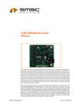
EVB8700 User Manual Copyright © 2007 SMSC or its subsidiaries. All rights reserved. Circuit diagrams and other information relating to SMSC products are included as a means of illustrating typical applications. Consequently, complete information sufficient for construction purposes is not necessarily given. Although the information has been checked and is believed to be accurate, no responsibility is assumed for inaccuracies. SMSC reserves the right to make changes to specifications and product descriptions at any time without notice. Contact your local SMSC sales office to obtain the latest specifications before placing your product order. The provision of this information does not convey to the purchaser of the described semiconductor devices any licenses under any patent rights or other intellectual property rights of SMSC or others. All sales are expressly conditional on your agreement to the terms and conditions of the most recently dated version of SMSC's standard Terms of Sale Agreement dated before the date of your order (the "Terms of Sale Agreement"). The product may contain design defects or errors known as anomalies which may cause the product's functions to deviate from published specifications. Anomaly sheets are available upon request. SMSC products are not designed, intended, authorized or warranted for use in any life support or other application where product failure could cause or contribute to personal injury or severe property damage. Any and all such uses without prior written approval of an Officer of SMSC and further testing and/or modification will be fully at the risk of the customer. Copies of this document or other SMSC literature, as well as the Terms of Sale Agreement, may be obtained by visiting SMSC’s website at http://www.smsc.com. SMSC is a registered trademark of Standard Microsystems Corporation (“SMSC”). Product names and company names are the trademarks of their respective holders. SMSC DISCLAIMS AND EXCLUDES ANY AND ALL WARRANTIES, INCLUDING WITHOUT LIMITATION ANY AND ALL IMPLIED WARRANTIES OF MERCHANTABILITY, FITNESS FOR A PARTICULAR PURPOSE, TITLE, AND AGAINST INFRINGEMENT AND THE LIKE, AND ANY AND ALL WARRANTIES ARISING FROM ANY COURSE OF DEALING OR USAGE OF TRADE. IN NO EVENT SHALL SMSC BE LIABLE FOR ANY DIRECT, INCIDENTAL, INDIRECT, SPECIAL, PUNITIVE, OR CONSEQUENTIAL DAMAGES; OR FOR LOST DATA, PROFITS, SAVINGS OR REVENUES OF ANY KIND; REGARDLESS OF THE FORM OF ACTION, WHETHER BASED ON CONTRACT; TORT; NEGLIGENCE OF SMSC OR OTHERS; STRICT LIABILITY; BREACH OF WARRANTY; OR OTHERWISE; WHETHER OR NOT ANY REMEDY OF BUYER IS HELD TO HAVE FAILED OF ITS ESSENTIAL PURPOSE, AND WHETHER OR NOT SMSC HAS BEEN ADVISED OF THE POSSIBILITY OF SUCH DAMAGES. SMSC EVB8700 USER MANUAL Revision 0.7 (07-24-07) rev E EVB8700 User Manual 1 Introduction The LAN8700 is a low-power, small form factor, highly integrated analog interface IC for highperformance embedded Ethernet applications. The LAN8700 requires only a single +3.3v supply, and has an integrated +1.8v supply to run the core digital logic. The EVB8700 is a customer evaluation board that interfaces a standard 40 pin MII connector from an existing MAC controller to the SMSC LAN8700 Ethernet PHY, and out to an RJ-45 Ethernet Jack for 10/100 connectivity. 1.1 References Concepts and material available in the following documents may be helpful when reading this document. Table 1.1 References DOCUMENT LOCATION SMSC LAN8700 Datasheet SMSC LAN8187 Datasheet http://www.smsc.com/main/datasheet.html AN13-9 Migrating from the LAN83C183 10/100 PHY to the LAN83C185 10/100 PHY AN13-2 Scalable Reference Design for Migrating from the SMSC LAN83C185 Non Auto MDIX to a Future SMSC LAN8187 HP Auto MDIX Configuration AN8-13 Suggested Magnetics http://www.smsc.com/main/appnotes.html Revision 0.7 (07-24-07) rev E USER MANUAL 2 SMSC EVB8700 EVB8700 User Manual 2 Details The EVB8700 shown in Figure 2.1 is a Daughter Card designed to plug into a user's test system, using the 40 pin MII connector. The MII connector is an AMP 40 pin Right Angle through hole MII connector, PN AMP-174218-2, reference designator P1. The mating connector is PN AMP 174217-2. The pinout for the plug is shown in Table 2.8. P1 40pin MII Reset Button MII interface test points SMSC LAN8700 Test Points Speed and Duplex LEDs 3.3V and 5V LEDs RJ-45 Ethernet Magnetic H1102 commercial temperature H1188 Industrial temperature Figure 2.1 Top View of the EVB8700 Note: Actual board may vary. 2.1 Power Power is provided to the on board +3.3v regulator by the +5v power coming from the MII connector P1. Standby power of +5v can be supplied externally by the test point loop at TP3 with ground connected to pin 20 of header J2. 2.1.1 +3.3 Volt Power Supply The EVB8700 has an on-board step down DC-DC +3.3v power supply regulator and uses the +5v input from the MII. 2.2 Configuration This section documents the configuration options available on the SMSC EVB8700. SMSC EVB8700 USER MANUAL 3 Revision 0.7 (07-24-07) rev E EVB8700 User Manual 2.2.1 PHY Address and LEDs Resistors R50, R51, R45, R46, R44, R47, R33, R35, R34, R36, R52, and R53 are used to set the PHY address according to Table 2.8. Table 2.1 PHY address and LED configuration NET NAME PHY ADDRESS SPEED100LED LSB PHYAD0 = 1 LSB PHYAD0 = 0 DEFAULT ACTIVE LOW Depopulate [R37, R51] Populate [R50] LED1 ACTIVE HIGH orient up Populate [R37, R51] Depopulate [R50] LED1 orient down LINKLED PHYAD1=1 PHYAD1=0 DEFAULT ACTIVE LOW Depopulate [R38, R44, R47] Populate [R45, ACTIVE HIGH R46] Populate [R38, R44, R47] Depopulate [R45, R46] ACTIVITYLED PHYAD2=1 PHYAD2=0 DEFAULT ACTIVE LOW Depopulate [R34,R36, R39] Populate [R33, ACTIVE HIGH R35] Populate [R34, R36, R39] Depopulate [R33, R35] FULLDUPLEXLED PHYAD3=1 PHYAD3=0 DEFAULT ACTIVE LOW Depopulate [R53, R40] Populate [R52] LED4 ACTIVE HIGH orient up Populate [R53, R40] Depopulate [R52] LED4 orient down CRS/PHYAD4 LED OUTPUT MSB PHYAD4 = 1 DEFAULT MSB PHYAD4=0 DESCRIPTION Depopulate [R49] Populate [R49] The address lines are strapped as defined in the diagram below. The LED outputs will automatically change polarity based on the presence of an external pull-down resistor. If the LED pin is pulled high, by the internal 100K pull-up resistor, the LED output will be active low. If the LED pin is pulled low, by an external 10K pull-down resistor, the LED output will be active high. To set the PHY address on the PHYAD pins, float the pin to set the address high or pull-down the pin with an external 10K resistor to GND to set the address low. See the Figure 2.2 below: Figure 2.2 PHY Address Strapping with the LED pins. Revision 0.7 (07-24-07) rev E USER MANUAL 4 SMSC EVB8700 EVB8700 User Manual 2.2.2 Boot Mode Configuration Options There are three resistors used to bootstrap the PHY into a specific mode. Table 2.2below shows how to populate the resistor to configure the PHY into different modes upon bootup (after reset). Table 2.2 PHY Address Configuration Resistors MODE2 R32 MODE1 R15 MODE0 R16 Empty Empty Empty All Capable Auto Negotiate Enable [Default] 111 Empty Empty Populated Powerdown mode startup (Note 2.1) 110 Empty Populated Empty Repeater Mode (Note 2.2): 100Base-TX Half Duplex is advertised Auto-negotiate enabled CRS is active during Receive 101 Empty Populated Populated 100Base-TX Half Duplex is Advertised. Auto-negotiation is enabled. CRS is active during Transmit and Receive. 100 Populated Empty Empty 100Base-TX Full Duplex. Auto-negotiate disabled. CRS is active during receive. 011 Populated Empty Populated 100Base-TX Half Duplex. Auto-negotiation disabled. CRS is active during transmit and receive. 010 Populated Populated Empty 10Base-T Full Duplex. Auto-negotiation disabled. 001 Populated Populated Populated 10Base-T Half Duplex. Auto-negotiation disabled. 000 BOOT MODE DESCRIPTION MODE REGISTER BITS MODE [2:0] Note 2.1 Please refer to the datasheet section 5.4 for more information on Powerdown mode. Note 2.2 Please refer to the datasheet section 5.4 for more information on Repeater mode. Note: An Empty resistor means an internal pull-up will bootstrap the Mode pin high to a logic 1. A Populated resistor will bootstrap the Mode pin low to a logic 0. 2.2.3 Pin 1 mode configuration Pin 1 can either be configured to drive nINT (Active low output interrupt pin) or to drive TXER/TXD4 (Transmit Error pin or Transmit Data 4). This bootstrapping option is controlled by R25 on the board, which is a 10k pull-down to ground on RXD3/nINTSEL. Normally this resistor is empty and the pin is pulled high internally. This default is to configure pin 1 option as nINT. To change this to a TXER pin, the user needs to populate R25. Refer to the LAN8700 datasheet for instructions on changing the TXER pin to a TXD4 pin. 2.2.4 Digital Communications Mode Resistor R7 will change the digital communications mode of the LAN8700 PHY. By default this resistor is empty. An empty resistor defaults the pin to low at bootup and configures the PHY for MII communication. If R7 is populated with a 10k resistor, then the device will boot up in RMII mode. See Chapter 3 for more details. SMSC EVB8700 USER MANUAL 5 Revision 0.7 (07-24-07) rev E EVB8700 User Manual 2.2.5 MDIO pullup Resistor R1 is used to give a pullup to the MDIO pin. Normally the resistor is not needed because the MAC that the PHY is interfacing to has a pull-up built into its system. 2.3 HP Auto-MDIX options The LAN8700 supports Auto-MDIX on the analog output pins. The EVB8700 supports disabling the Auto-MDIX through the MDIO interface to the Internal registers. Setting bit 15 of register 27 to a 1 will disable Auto-MDIX switching function. Please refer to the SMSC LAN8700 datasheet for more information. 2.4 LED indicators There are 6 LEDs on the board, 4 placed on the board as discrete components, and 2 on the RJ-45 connector. Table 2.3 LED indicators SCHEMATIC REFERENCE SILK SCREEN NAME DESCRIPTION LED1 SPEED 100 This LED indicates when the PHY is communicating in 100Base-TX mode. This LED will only come on when the PHY has a link established. LED2e LED2 This LED indicates that the link is communicating in Full Duplex. Green(link) LINK This LED indicates that a link to the other host has been made. Yellow(Act) ACT This LED indicates that there is communication activity on the Ethernet Link. D1 +5V This LED indicates that there is +5v power to the board D2 +3.3V This LED indicates that there is +3.3v power to the board. 2.5 Test Points Table 2.4 and Table 2.5 below identify the test points for debug purposes. Table 2.4 Test Points TEST POINTS DESCRIPTION TP3 +5v power TP7 VDDCORE (Note 2.3) Note 2.3 Revision 0.7 (07-24-07) rev E TEST POINTS TP5 DESCRIPTION +3.3v power supply output. VDDCORE is the internal +1.8v regulated output, that needs a 4.7uF and a 0.1uF capacitor to decouple the voltage. USER MANUAL 6 SMSC EVB8700 EVB8700 User Manual Table 2.5 Test Points From Header J2 HEADER PIN HEADER PIN DESCRIPTION DESCRIPTION 1 nRST: active low reset signal from the MII plug or the on board reset button SW1 11 TX_ER: Transmit Error 2 MDIO: Management Data Input Output. 12 TX_CLK: Transmit clock 3 MDC: Management Clock 13 TX_EN: Transmit Enable 4 RXD3: Receive Data Bit 3 14 TXD0: Transmit Data Bit 0. 5 RXD2: Receive Data Bit 2 15 TXD1: Transmit Data Bit 1 6 RXD1: Receive Data Bit 1 16 TXD2: Transmit Data Bit 2 7 RXD0: Receive Data Bit 0 17 TXD3: Transmit Data Bit 3 8 RX_DV: Receive Data Valid 18 COL: Collision Detected. 9 RX_CLK: Receive Clock 19 CRS: Carrier Sense. 10 RX_ER: Receive Error 20 Digital Ground Table 2.6 Test Points From Header J3 HEADER PIN HEADER PIN DESCRIPTION DESCRIPTION 1 nINT/TX_ER/TXD4: Multi-use pin. 2 VDDIO: I/O voltage test pin (Note 2.4) 3 VDD: Core VDD voltage. 4 Digital Ground Note 2.4 This pin can be used to drive a separate IO voltage, when the ferrite bead FB5 is Depopulated Table 2.7 Test Points From Header J4 HEADER PIN HEADER PIN DESCRIPTION DESCRIPTION 1 +5V from MII plug 2 Digital Ground 3 +5V from MII plug 4 Digital Ground SMSC EVB8700 USER MANUAL 7 Revision 0.7 (07-24-07) rev E EVB8700 User Manual 2.6 Connector Pin-outs 2.6.1 MII Connector The MII connector supplies +5v power to the board, as well as the digital control signals. The pinout for the connector is shown below in Table 2.8. Table 2.8 AMP MII Connector Pinout RA (P1) 1 +5V[3] 11 TX_ER (Note 2.5) 21 +5V[2] 31 GND[9] 2 MDIO 12 TX_CLK 22 GND[18] 32 GND[8] 3 MDC 13 TX_EN 23 GND[17] 33 GND[7] 4 RXD3 14 TXD0 24 GND[16] 34 GND[6] 5 RXD2 15 TXD1 25 GND[15] 35 GND[5] 6 RXD1 16 TXD2 26 GND[14] 36 GND[4] 7 RXD0 17 TXD3 27 GND[13] 37 GND[3] 8 RX_DV 18 COL 28 GND[12] 38 GND[2] 9 RX_CLK 19 CRS 29 GND[11] 39 GND[1] 10 RX_ER 20 +5V[4] 30 GND[10] 40 +5V[1] Note 2.5 2.6.2 TX_ER from the MII is not used on the EVB8700, but can be monitored on the test header J2. MII Pin Description The signals are defined in Table 2.9 with a description relative to the EVB8700 Table 2.9 MII 40 Pin Description NAME DIRECTION RELATIVE TO EVB8700 ACTIVE LEVEL GND[18-1] Power n/a Ground Plane. +5V[4-1]] Power n/a +5v supply from the MII connector. Converted to +3.3v on the EVB and used to power the LAN8700 PHY and +3.3v rail. RXD[3-0] Output TBA Receive data bits 0 to 3 that are sent by the PHY to the receive path of the MII connector to the MAC controller. TXD[3-0] Input TBA Transmit data bits 0 to 3 that are accepted by the PHY in the receive path from the MAC controller. MDIO Input/Output TBA Management Data Input Output: serial management data input/output. MDC Input TBA Management Data Clock: clock signal for the above MDIO signal. Revision 0.7 (07-24-07) rev E DESCRIPTION USER MANUAL 8 SMSC EVB8700 EVB8700 User Manual Table 2.9 MII 40 Pin Description 2.6.3 NAME DIRECTION RELATIVE TO EVB8700 ACTIVE LEVEL RX_DV Output TBA Receive data valid: this signal indicates that recovered and decoded data nibbles are being presented on RXD[3:0]. RX_CLK Output TBA Receive Clock: 25MHz in 100base-TX mode. 2.5MHz in 10baseT mode. RX_ER Output TBA Receive Error: Asserted to indicate that an error was detected somewhere in the frame presently being transferred from the PHY. TX_ER Input/Output TBA Transmit Error or Transmit data 4: This bit is set by the RXD3/nIntsel pin. TX_CLK Output TBA Transmit Clock: 25MHz in 100base-TX mode. 2.5MHz in 10baseT mode. TX_EN Input TBA Transmit Enable: Indicates that valid data is present on the TXD[3:0] signals, for transmission. COL Output TBA MII Collision detection: Assertion to indicate detection of collision. CRS Output TBA Carrier Sense: Assertion indicates detection of carrier. DESCRIPTION RJ-45 Ethernet Jack The pinout for the RJ-45 Jack is described in Table 2.10 below. Table 2.10 RJ-45 Ethernet Jack Pin-Out PIN DESCRIPTION 1 TXP: Transmit Positive 2 TXN: Transmit Negative 3 RXP: Receive Positive 4 Analog Reference to ground 5 Analog Reference to ground 6 RXN: Receive Negative 7 Analog Reference to ground 8 Analog Reference to ground SMSC EVB8700 USER MANUAL 9 Revision 0.7 (07-24-07) rev E EVB8700 User Manual 2.7 Clocking 2.7.1 Crystal Oscillator The 25 MHz crystal Y1 is connected to the internal oscillator of the LAN8700. A PLL circuit in the LAN8700 generates all the timing needed by the PHY. 2.7.2 External Clock The board can be configured to use an external clock if the crystal Y1 is removed and a 25MHz +2.0v signal is injected onto pin Y1.1 which is connected to pin 14 of the LAN8700. Y1.2 (pin 13 of the LAN8700) is left floating. Revision 0.7 (07-24-07) rev E USER MANUAL 10 SMSC EVB8700 EVB8700 User Manual 3 RMII Configuration The first section of this chapter provides detailed instructions to modify an existing EVB8700 rev E board to make it operate in RMII mode. The second section describes using the RMII modified EVB board in a customer's application. 3.1 Modifications to the EVB8700 There are four modifications needed to the EVB8700 to make it run in RMII mode. 1. Crystal Circuit - Remove crystal Y1 and resistor R48. 2. RMII mode pin - Add resistor R7. 3. 50MHz clock - The system must supply a 50MHz clock. 3.1.1 Crystal circuit Remove Y1 and R48 from the crystal circuit as the 25MHz crystal is not needed. Also the 1Meg ohm resistor is not needed. 3.1.2 RMII mode pin Populate resistor R7 with a 10k ohm 0603 resistor. This will boot strap the EVB8700 into RMII digital communications mode. 3.1.3 50MHz Clock Source The digital communication between the LAN8700 and the MAC requires a single 50MHz clock source for both devices. This can be added in several ways. The easiest is to add a crystal oscillator chip (ECS Inc PN:ECS-3963-500-BN-TR) to the EVB module as shown in Figure 3.1. A footprint is not provided on the board. The 50MHz source also needs to go into the MAC clock control circuit. This can easily be accommodated by using the RX_CLK pin, since its not used in RMII mode. To use the RX_CLK pin, remove resistor R21, then using a wire, make a connection from the 50MHz clock source, to pin 9 of J2. This will provide 50MHz clock to the PHY at X1, and 50MHz clock to the MAC through the MII plug RX_CLK pin. If the customers board doesn’t have an MII plug, then the customer can add a wire to the EVB into the header plug at J2. The 50MHz clock source for the MAC would come from the RX_CLK on the header. The alternative solution is to add a 50MHz source from the system. The RX_CLK pin can also be used, just remove R21, and connect a wire from the MII plug side of R21 to the CLKIN side of the Y1 crystal. SMSC EVB8700 USER MANUAL 11 Revision 0.7 (07-24-07) rev E EVB8700 User Manual Figure 3.1 Add a 50MHz Oscillator to the EVB8700 for RMII Mode Table 3.1 RMII Connections Using the Debug Header J2 of the EVB8700 EVB8700 SILK SCREEN HEADER J2 NAME J2 PIN NUMBER RMII NAME MAC NAME COMMENT nRST 1 nRST nRST This signal is used to reset the PHY on the EVB MDIO 2 MDIO MDIO Optional, used to read/write the internal registers of the PHY. MDC 3 MDC MDC Optional. clock signal used to read/write the registers of the PHY RXD3 4 Not used in RMII mode RXD2 5 Not used in RMII mode Revision 0.7 (07-24-07) rev E USER MANUAL 12 SMSC EVB8700 EVB8700 User Manual Table 3.1 RMII Connections Using the Debug Header J2 of the EVB8700 (continued) EVB8700 SILK SCREEN HEADER J2 NAME J2 PIN NUMBER RMII NAME MAC NAME COMMENT RXD1 6 RXD1 RXD1 Receive data 1 RXD0 7 RXD0 RXD0 Receive data 0 RX_DV 8 RCLK 9 CLKIN REFclk This header pin and MII plug pin can be used as the 50MHz port between the PHY and the MAC. (Note 3.1) RX_ER 10 RX_ER RXER Optional for the MAC. Required by the PHY. The MAC can choose to ignore this signal. TXER 11 Not used. TXCLK 12 Not used. TX_EN 13 TX_EN TX_EN Transmit enable. TXD0 14 TXD0 TXD0 Transmit data bit 0 TXD1 15 TXD1 TXD1 Transmit data bit 1 TXD2 16 Not used in RMII mode, these can be tied directly to GND. TXD3 17 Not used in RMII mode, these can be tied directly to GND. COL 18 CRS 19 GND 20 Not used in RMII mode CRS_DV CRSDV Carrier Sense and Data Valid This pin is not used in RMII mode. GND GND Ground connection to VSS. J3 extension of J2 TXD4 1 Not used in RMII mode. VDDIO 2 VDDIO VDDIO Variable Voltage IO (+1.8V to +3.6V) to match IO voltage of MAC. (Note 3.2) VDD 3 VDD +3.3V +3.3V power to drive analog and core GND 4 GND GND Ground connection to VSS. J4 extension of J2 +5 1 +5V +5V +5V power. GND 2 GND GND Ground connection to VSS. +5 3 +5V +5V +5V power. 4 GND GND Ground connection to VSS. Note 3.1 By Default this is connected to +3.3V on the EVB8700. To isolate this power and drive separately, remove FB5. Note 3.2 By Default this is connected to +3.3V on the EVB8700. To isolate this power and drive separately, remove FB5. SMSC EVB8700 USER MANUAL 13 Revision 0.7 (07-24-07) rev E EVB8700 User Manual 3.2 How to use the RMII configured EVB8700 The easiest way to use the EVB8700 configured for RMII mode, is to have an MII plug designed into your system so that the EVB8700 can plug directly in. The pinout is shown below in Figure 3.2 Figure 3.2 MII Plug Pinout If the system doesn’t have an MII plug, then the EVB8700 has a debug header J2 which can be used to wire in the EVB to the system, using the RMII pins identified in column 3 of Table 3.1. Revision 0.7 (07-24-07) rev E USER MANUAL 14 SMSC EVB8700 SMSC EVB8700 USER MANUAL 15 A B C D 5 Board: Chip: Board Form Factor: Assembly: Design Details 5 MII CONNECTOR MII Bus 4 LAN8700(I) 10/100 Magnetics 3 RJ45 Schematic Revision E0 +3.3V I/O VDDIO Operation EVB BLOCK DIAGRAM PCB-7054AZ-E0 LAN8700(I) 2 EVB-LAN8700 3 1 2 1 12/6/05 12/12/05 12/15/05 1/16/06 Rev E0 2/24/06 Rev D1 Rev D2 Rev D3 Rev D4 Revisions 4 Date: Size C Title 1 Sheet SCH-7054AZ LAN8700(I) MII EVB Tuesday, April 18, 2006 Document Number 1 of 4 3930 East Ray Road Suite 200 Phoenix, Arizona 85044 480-759-0200 Customer Public version created from D1 Corrected for the industrial temp capacitance Corrected for REGOFF pin polarity change INTR to header; increased test header to 24p intr to vddio; moved .01uf to vddio and added 10uf to vddio; added intersheet references. Reference Design for A0 silicon with +3.3V I/O VDDIO Power & Misc 3 2 LAN8700(I) & Magnetics Stackup and Layout Page Title Page ITEM Circuit Diagrams utilizing SMSC Products Are Included As A Means Of Illustrating Typical Semiconductor Applications: Consequently Complete Information Sufficient For Construction Purposes Is Not Necessarily Given. The Information Has Been Carefully Checked And Is Believed To Be Entirely Reliable. However, No Responsibility Is Assumed For Inaccuracies. Furthermore, Such Information Does Not Convey To The Purchaser Of The Semiconductor Devices Described Any License Under The Patent Rights Of SMSC Or Others. SMSC Reserves The Right To Make Changes At Any Time In Order To Improve Design And Supply The Best Product Possible. LAN8700(I) MII Customer Evaluation Board 4 E0 Rev A B C D EVB8700 User Manual Revision 0.7 (07-24-07) rev E Revision 0.7 (07-24-07) rev E USER MANUAL 16 A B 5 stackup soldermask (bottom) Silkscreen (bottom) layer 4 (1 oz copper .0014) prepreg .010 4 Layer 3 Power plane (1 oz copper .0014) C-stage Core .039 layer 2 Ground plane (1 oz copper .0014) prepreg .010 silkscreen (top) soldermask (top) layer 1 (1 oz copper .0014) 3 NOTES: 1. BOARD FABRICATION AND QUALITY ACCEPTANCE PER IPC-6012 CLASS 2. BOARD MUST MEET OR EXCEED QUALIFICATION TESTING AND QUALITY CONFORMACE TESTING INSPECTION SPECIFIED WITHIN. 2. MATERIAL: NEMA GRADE STANDARD FR4. LAMINATED SHEET, HTE 1 OZ COPPER CLAD, TYPE GF/GFG WOVEN GLASS BASE, FLAME RESISTANCE MEETING UL94V-0 OR BETTER. MATERIAL IN ACCORDANCE WITH IPC-4101. 3. BOARD FABRICATION SHALL APPLY DATE CODE, FABRICATOR'S CAGE CODE, I.D. AND UL MARKING TO SECONDARY SIDE WHERE INDICATED. MARKING PREFERABLY COPPER ETCHED. EPOXY INK ACCEPTABLE. 4. SOLDERMASK,USING TYPEB,PHOTO IMAGEABLE LPI FILM 0.0015 THICK. APPLY TO BOTH SIDES IN ACCORDANCE WITH IPC-SM-840 (TYPE B CLASS 3). USE APPROPIATE SOLDER MASK ARTWORK FOR EACH SIDE. PUNCTURING OF PUNCTURING OF TENTED HOLES IS PERMISSIBLE. SOLDERMASK MISREGISTRATION SHALL NOT EXCEED .004 INCH. SOLDERMASK OVERLAP PERMITTED ON CIRCULAR LANDS ONLY AND SHALL NOT EXCEED 0.001 INCH. NO OVERLAP PERMITTED ON RECTANGULAR LANDS. 5. FINISH: SOLDER MASK OVER BARE COPPER (SMOBC), HOT AIR LEVEL DEPOSIT 6. DRILL BOARDS USING DRILL DATA, DRILL PATTERN AND HOLE SCHEDULE. HOLE LOCATION MAY VARY WITHIN .004 IN. MAX ABOUT TRUE POSITION. 7. MINIMUM ANNULAR RINGS: .002 IN MINIMUM - EXTERNAL LAYERS. .001 IN MINIMUM - INTERNAL LAYERS. 8. ALL EXPOSED SURFACE LANDS AND LINES TO BE SOLDER COATED. 9. ALL HOLES ARE PLATED THROUGH UNLESS NOTED OTHERWISE. MINIMUM COPPER PLATING IN PLATED HOLES TO BE .001 IN. COPPER PLATING IN TENTED HOLES SHALL NOT PLUG HOLES WITHOUT PERMISSION FROM SMSC. 10. COMPONENT MARKINGS: SILKSCREEN BOTH SIDES USING NONCONDUCTIVE WHITE EPOXY INK. LANDS AND EXPOSED PLATED AREAS TO BE FREE OF INK. 11. DIMENSIONS ARE AFTER ETCHING AND PLATING AND ARE BASIC UNLESS OTHERWISE INDICATED. 12. BARE BOARD ELECTRICAL TEST: BARE BOARDS SHALL BE ELECTRICALLY TESTED USING CAD GENERATED NET LIST DATA. THIS INFORMATION TO BE SUPPLIED IN IPC-D-356 FORMAT. ELECTRICAL TESTING SHALL FOLLOW THE GUIDELINES EXTABLISHED BY IPC-ET-652. GUIDELINES AND REQUIREMENTS FOR ELECTRICAL TESTING OF PRINTED WIRING BOARDS. 2 Title Date: Size C 3930 East Ray Road Suite 200 Phoenix, Arizona 85044 480-759-0200 1 Sheet SCH-7054AZ Tuesday, April 18, 2006 Document Number LAN8700(i) MII EVB 1 2 of 4 E0 Rev A B C 2 C 3 D 4 D 5 EVB8700 User Manual SMSC EVB8700 USER MANUAL 17 A B C D TX_CLK TX_EN 4 TXD0 4 TXD1 4 TXD2 4 TXD3 4 COL 4 CRS 4 111 110 101 100 011 010 001 000 5 Empty (Default) nINT Populated TXER/TXD4 R25 pin 1 mode Mode 0 R16 Empty Populated Empty Populated Empty Populated Empty Populated R13 R14 4 1% 1% 1M C7 30pF 50V 5% 25Mhz Y1 VDDIO C8 30pF 50V 5% nRESET 1% R16 10.0K 1/10W DNP mode0 R7 10.0K 1/10W DNP 1% R48 R15 10.0K 1/10W DNP R32 10.0K 1/10W DNP nRESET mode1 mode2 R12 10.0K 1/10W DNP 1% All Capable [Default] Power Down Mode Repeater Mode 100Base-TX Half duplex Advertised 100Base-TX Full Duplex Auto Negotiate 100Base-TX Half Duplex Auto Negotiate 10Base-T Full Duplex Auto Negotiate 10Base-T Half Duplex Auto Negotiate 10R 10R R23 R18 R17 R10 R11 R19 R21 R22 10R 10R 10R 10R 10R 10R 10R 10R R9 10R CRS/PHYAD4 TX_CLK TX_EN TXD0 TXD1 TXD2 TXD3 COL CRS MDIO MDC RXD3 RXD2 RXD1 RXD0 RX_DV RX_CLK RX_ER BootStrap Options Mode 2 Mode 1 R32 R15 Empty Empty Empty Empty Empty Populated Empty Populated Populated Empty Populated Empty Populated Populated Populated Populated 4 4 MDIO 4 MDC 4 RXD3 4 RXD2 4 RXD1 4 RXD0 4 RX_DV 4 RX_CLK 4 RX_ER R12 Internal Regulator Disable Depopulated (Default) Enabled (ON) Internal 1.8v regulator Populated Disabled (OFF) Internal 1.8v regulator Depopulate ( Default) MII mode Populate RMII mode R7 Digital communications mode BootStrap Options DNP 1% 13 14 5 22 6 23 24 26 27 36 3 4 2 15 16 17 18 19 20 21 R25 10.0K 1/10W 1% R1 1.50K 1/10W VDD F-BEAD 500mA / 0.1DCR FB5 XTAL2 CLKIN/XTAL1 nRST TX_CLK TX_EN TXD0 TXD1 TXD2 TXD3 COL/MII/CRS_DV CRS/PHYAD4 4 MDIO MDC RXD3/nINTSEL RXD2/MODE2 RXD1/MODE1 RXD0/MODE0 RX_DV RX_CLK/REGOFF RX_ER/RXD4 VDDIO AVDD U2 F-BEAD 500mA / 0.1DCR FB2 R54 12.4K 1/10W 1% LAN8700(I) 25 VDDIO +3.3V 7 R1 Pullup to 5v on MDIO Serial line. Normally pulled high in the system by the MAC. TXP RXN RXP TXN 8 1 C6 4.7uF 6.3V 20% VDDCORE C1 15pF 50V DNP R37 10.0K 1/10W DNP 1% LED Output PHY address '11111' = 0x1F = 31d 4 RD- RCT RD+ VDDIO R51 330R DNP 5% GREEN LED LED1 3 ZERO 1/4W 5% R55 Depopulate [R37, R51] Populate [R50] LED1 orient up Populate [R37, R51] Depopulate [R50] LED1 oreint down Depopulate [R38, R44, R47] Populate [R45, R46] Populate [R38, R44, R47] Depopulate [R45, R46] Depopulate [R34,R36, R39] Populate [R33, R35] Populate [R34, R36, R39] Depopulate [R33, R35] Depopulate [R53, R40] Populate [R52] LED4 orient up Populate [R53, R40] Depopulate [R52] LED4 oreint down Depopulate [R49] Populate [R49] 330R R50 1CT:1CT TD- TCT TD+ T1 HX1188 R40 R49 10.0K 10.0K 1/10W 1/10W DNP DNP 1% 1% 8 7 6 3 2 1 R8 10R 1/10W 1% C3 0.022uF 50V 10% Resistor configuration TEST_POINT Default Active Low Active High Default Active Low Active High Default Active Low Active High Default Active Low Active High Default C30 0.1uF 16V 10% TP7 R6 49R9 1/16W 1% FB4 F-BEAD 500mA / 0.1DCR +3.3V R38 R39 10.0K 10.0K 1/10W 1/10W DNP DNP 1% 1% C2 15pF 50V DNP R5 49R9 1/16W 1% TRVDD2 nINT/TX_ER/TXD4 SPEED100LED LINKLED ACTIVITYLED FULLDUPLEXLED CRS/PHYAD4 PHY address LSB PHYAD0 = 1 LSB PHYAD0 = 0 PHYAD1 = 1 LED2 PHYAD1 = 0 PHYAD2 = 1 LED3 PHYAD2 = 0 PHYAD3 = 1 LED4 PHYAD3 = 0 MSB PHYAD4 = 1 MSB PHYAD4 = 0 LED1 VDD_CORE nINT/TX_ER/TX4 9 10 11 12 RXN 31 R3 49R9 1/16W 1% TRVDD1 Layout note: keep C1 and C4 close to U2 RXP TXN TXP R2 49R9 1/16W 1% 500mA / 0.1DCR FB1 F-BEAD +3.3V 32 28 29 F-BEAD 500mA / 0.1DCR FB3 SPEED100/PHYAD0 LINK/PHYAD1 ACTIVITY/PHYAD2 FDUPLEX/PHYAD3 VDD33A1 VDD33A2 VDD33A3 3 330R R52 VDDIO NC1 4 VDD33 EXRES1 34 NC2 5 30 33 35 VSS/FLAG 37 NC3 12 4 2 1 NC4 13 2 SMSC EVB8700 1 5 R53 330R DNP 5% GREEN LED LED2 TCM_ RX- RX+ TCM TX- TX+ 75R0 1/16W 0.5% R26 10 9 11 15 14 16 2 2 C4 <voltage> 1000pF 1KV 10% 75R0 1/16W 0.5% R27 R28 49R9 R41 49R9 1/16W 1% R30 49R9 C5 <voltage> 1000pF 1KV 10% R29 49R9 R42 49R9 1/16W 1% Date: Size C CAT2 CAT1 RJ1 RJ2 RJ3 RJ4 RJ5 RJ6 RJ7 RJ8 ACTIVITYLED ANODE1 VDDIO 330R R46 330R R35 YELLOW (ACT) ANODE2 GREEN (LINK) R47 330R DNP R36 330R DNP 5% 16 14 10 9 12 11 Tuesday, April 18, 2006 1 Sheet SCH-7054AZ LAN8700(I) MII EVB Document Number 3 of 4 3930 East Ray Road Suite 200 Phoenix, Arizona 85044 480-759-0200 configuration resistor compliments * Note: The (i) designates industrial temperature LAN8700i PHY (-40c to +85c). For industrial temperature applications, SMSC recommends using the LAN8700i with industrial temperature magnetics. For Commercial temperature magnetics, capacitor C1 and C4 can be depopulated. Plese refer to APP note 8.13 Magnetics Selection Guide". LINKLED R44 ZERO 0.1W DNP 5% HOLE1 HOLE2 SHIELD1 SHIELD2 VDDIO J1 RJ45_LEDS R34 ZERO 0.1W R33 DNP ZERO 5% 0.1W 5% R45 ZERO 0.1W 5% Title R31 49R9 15 13 1 2 3 4 5 6 7 8 1 E0 Rev A B C D EVB8700 User Manual Revision 0.7 (07-24-07) rev E A B C D +5V +5V 40 39 38 37 36 35 34 33 32 31 30 29 28 27 26 25 24 23 22 21 5 AMP - 174218-2 THD_PLASTIC_PLUG MII_RA +5V[1] COMMON[1] COMMON[2] COMMON[3] COMMON[4] COMMON[5] COMMON[6] COMMON[7] COMMON[8] COMMON[9] COMMON[10] COMMON[11] COMMON[12] COMMON[13] COMMON[14] COMMON[15] COMMON[16] COMMON[17] COMMON[18] +5V[2] P1 +5V[3] MDIO MDC RXD3 RXD2 RXD1 RXD0 RX_DV RX_CLK RX_ER TX_ER TX_CLK TX_EN TXD0 TXD1 TXD2 TXD3 COL CRS +5V[4] 1 2 3 4 5 6 7 8 9 10 11 12 13 14 15 16 17 18 19 20 +5V +5V MDIO MDC RXD3 RXD2 RXD1 RXD0 RX_DV RX_CLK RX_ER TX_ER TX_CLK TX_EN TXD0 TXD1 TXD2 TXD3 COL CRS + C23 10uF 16V VDDIO C14 0.01uF 16V 10% MDIO 3 MDC 3 RXD3 3 RXD2 3 RXD1 3 RXD0 3 RX_DV 3 RX_CLK 3 RX_ER 3 TX_ER TX_CLK 3 TX_EN 3 TXD0 3 TXD1 3 TXD2 3 TXD3 3 COL 3 CRS 3 C21 0.01uF 16V 10% TRVDD1 4 C15 0.01uF 16V 10% 4 C26 4.7uF 6.3V VDD C16 0.01uF 16V 10% +5V TEST_POINT Orange C24 4.7uF 6.3V TP3 C17 0.01uF 16V 10% C22 0.01uF 16V 10% C10 10uF 16V C18 0.01uF 16V 10% AVDD + TRVDD2 C9 0.1uF 16V 10% VR2 C19 0.01uF 16V 10% Vin C27 4.7uF 6.3V 3 +5V MII to +3.3V Regulator GND 1 2 4 800mA 3 3 C20 0.01uF 16V 10% LT1117-3.3 Vout Vout 3 nRESET + C25 4.7uF 6.3V C11 10uF 16V SW-PB SW1 TEST_POINT Yellow C12 0.01uF 50V 10% TP5 +3.3V MH 1 MH 1 MTG250P125D MH2 MTG250P125D MH1 C13 0.1uF 16V R56 10.0K 1/10W 1% VDDIO 1.5 A Max Current from Reg 3 3 MDC 3 RXD2 3 RXD0 3 RX_CLK TX_ER 3 TX_EN 3 TXD1 3 TXD3 3 CRS 2 nINT/TX_ER/TXD4 2 +5V VDD 1 3 1 3 1 3 5 7 9 11 13 15 17 19 R43 10.0K 1/10W 1% VDDIO MDC RXD2 RXD0 RX_CLK TX_ER TX_EN TXD1 TXD3 CRS 2 4 6 8 10 12 14 16 18 20 2 4 2 4 Date: Size C Title HDR_2x2 J4 HDR_2x2 J3 R57 510R 1/10W 5% D1 LED GREEN 1 D2 LED GREEN Sheet 4 of 4 3930 East Ray Road Suite 200 Phoenix, Arizona 85044 480-759-0200 R58 330R 1/16W 5% +3.3V SCH-7054AZ Tuesday, April 18, 2006 Document Number +5V Layout Note: Place J2 J3 and J4 in single row MDIO 3 RXD3 3 RXD1 3 RX_DV 3 RX_ER 3 TX_CLK 3 TXD0 3 TXD2 3 COL 3 LAN8700(I) MII EVB MDIO RXD3 RXD1 RX_DV RX_ER TX_CLK TXD0 TXD2 COL HDR_2x10 J2 1 1 18 2 USER MANUAL 1 Revision 0.7 (07-24-07) rev E 2 5 E0 Rev A B C D EVB8700 User Manual SMSC EVB8700