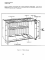
1
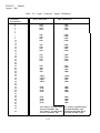
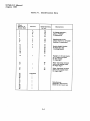
 XVME-212
6U 32-Channel Digital Input Module
USER’S MANUAL
ACROMAG INCORPORATED
30765 South Wixom Road
P.O. BOX 437
Wixom, MI 48393-7037 U.S.A.
Tel: (248) 295-0885
Fax: (248) 624-9234
Email: [email protected]
Copyright 2012, Acromag, Inc., Printed in the USA.
Data and specifications are subject to change without notice.
8500-967B XVME-212 Manual
August, 1989
Chapter 1
INTRODUCTION
1.1
INTRODUCTION
The XVME-212 is a 32 channel, opto-isolated, digital input interface, designed to be
compatible with the VMEbus structure. The XVME-212 is capable of receiving 32 digital
inputs at frequencies up to 3.4 KHz. To ensure signal integrity, the design incorporates
integrated “switch” debouncing, as well as the protection provided by the optical isolation
of the channel inputs from the system bus structure. In addition, an on-board scanner can
be programmed to generate a VMEbus interrupt when any input changes state, thus
eliminating the need to poll the input module.
Each digital input is reverse voltage protected and is capable of handling a maximum
reverse bias of 50V DC (XVME-212/l) or 6.5V DC (XVME-212/2). Also, the board can be
jumpered to occupy any 1K block within the short I/O address space.
The following two versions of the XVME-212 are available:
XVME-212/l -- The /l version of the XVME-212 comes with an on-board, 12V DC,
isolated power supply. The 12V supply is factory-connected to the input of each channel,
thus permitting the system to monitor 12V relay contacts and switches without an external
power supply. Voltages other than the 12V may be applied to the inputs (within the l0V50V input range); however, some board modification will be necessary (i.e., cutting the
well identified and easily accessible PC traces to the 12V on-board supply).
XVME-212/2 -- The /2 version of the XVME-212 is very similar to the /I version except
for the range of allowable input voltage and the absence of an on-board +12V DC power
supply. The XVME-212/2 has TTL level inputs with a 6.5V maximum input. In addition,
the +12V isolated, on-board power supply is not available, replaced by wire jumpers to
the existing +5V supply of the VME backplane.
1.2 MANUAL STRUCTURE
This first chapter provides a functional overview of the XVME-212 and presents the
features of Xycom’s Standard I/O architecture. Operational aspects of the XVME-212 are
then explained in the following fashion:
Chapter 2 -
Installation: Information required to position the jumpers and switches
on the XVME-212, and install the module in a VMEbus chassis.
Chapter 3 -
Programming: Information required to program the XVME-212 and
read digital input signals.
The appendices at the end of this manual provide information on Xycom’s Standard I/O
Architecture, VMEbus connector/pin descriptions, module schematics, as well as a quick
reference guide to the module’s jumpers and registers.
1-l
XVME-2 12 Manual
August, 1989
-
Module identification - The XVME-212 has ID information which provides its name,
model number, manufacturer, and revision level at a location that is consistent with
other Xycom I/O modules.
-
Status/Control Register - This register is always located at address base + 8 lH, and
the lower four bits (two Test Status bits, and a red and green LED bit) are standard
from module to module.
A detailed description of Xycom I/O Architecture is presented in Appendix A at the rear
of this manual.
1.5 XVME-212 MODULE SPECIFICATIONS
Table l-l. XVME-2 12 Module Specifications
/ Characteristic
/
’ Number of Channels
Specification
~ Input Voltage Range (XVME-212/l)
I
I
+5OV DC max.
Logic 1 -- 10 to 5OV DC
Logic 0 -- 0 to lV DC
Typical t h r e s h o l d- - 3 V DC
: Input Voltage Range (XVME-212/2)
+65V DC max.
Logic 1 -- 2 to 6.5V DC
Logic 0 -- 0 to 0.8V DC
Typical threshold -- 1.2V DC
1 Input Impedance (XVME-2 12/ 1)
: Input Impedance (XVME-2 12/2)
3.9K +5%
330 +5%
~ Propagation Delay
~ (with fastest debounce selected)
Of f-to-on
On-to-off
100 usec max. (l0-25 usec typ.)
600 usec max. (150 usec typ.)
~ Minimum Detectable Pulse Width
Positive pulse
II
Negative pulse
I
100 usec max. (l0-25 usec typ.)
600 usec max. (150 usec typ.)
~ Maximum Input Frequency
3.4 KHz typical
32
Debounce Time
Jumper-selectable from 4.5 usec to 18 msec
(8 possible settings)
Reverse Bias Protection (XVME-212/l) - 50 V max.
Reverse Bias Protection (XVME-2 12/2) - 6.5V max.
Power
Requirements
+5V, 25% 1.7 Amp typ., 2.0 Amp max.
1-3
XVME-2 12 Manual
August, 1989
Table l-l. XVME-2 12 Module Specifications (cont’d)
Characteristic
Specification
Isolation
300 VDC channel-to-channel
300 VDC channel to VMEbus ground
Board Dimensions
NEXP board size
(160mm x 233.4mm)
Environmental Specifications
Temperature
Operating
0’ to 65’C
(32’ to 149’F)
-40’ to 85’C
(-40’ to 158’F)
Non-operating
Humidity
5 to 95% RH, non-condensing
(Extremely low humidity conditions may
require special protection against static
discharge.)
Altitude
Operating
Sea level to 20,000 ft.
(6096m)
Sea level to 50,000 ft.
(15240m)
Non-operating
Vibration
Operating
Shock
I
5 to 2000 Hz
.O 15” peak-to-peak displacement
2.5g peak acceleration
Non-operating
5 to 2000 Hz
.030” peak-to peak displacement
5.0 g peak (maximum) acceleration
Operating
30 g peak acceleration,
11 msec duration
Non-operating
50 g peak acceleration,
11 msec duration
1-4
XVME-2 12 Manual
August, 1989
Table l- 1. XVME-2 12 Module Specifications (cont’d)
-~~
~~~-~
Characteristic
Specification
VMEbus Compliance
l
l
l
l
l
l
l
1-5
Fully compatible with VMEbus standard
Al 6:D16 Data transfer bus slave
Base address jumper-selectable within
64K short I/O address space
Occupies 1K consecutive byte locations
I(1) to I(7) Interrupter (STAT) with
programmable vector
Includes Xycom’s standard I/O module
interface
NEXP
XVME-212 Manual
August, 1989
Chapter 2
INSTALLATION
2.1 INTRODUCTION
This chapter provides the information needed to configure the XVME-212 and to install
it in a VMEbus backplane card cage.
2.2 SYSTEM REQUIREMENTS
The XVME-212 is a double-high VMEbus compatible module. To operate, it must be
properly installed in a VMEbus backplane cardcage. The minimum system requirements
for operation of the XVME-212 are one of the following (either A or B below):
A)
A host processor properly installed on the same backplane.
A properly installed controller subsystem. An example of such a control subsystem
is the Xycom XVME-010 System Resource Module.
-OR-
B)
A host processor which incorporates an on-board controller subsystem.
2.3
LOCATION OF COMPONENTS RELEVANT TO INSTALLATION
The
\ jumpers, switches, and connectors on the XVME-212 are illustrated in Figure 2-1.
2-1
XVME-212 Manual
August, 1989
2.4
JUMPERS/SWITCHES
Prior to installing the XVME-212, it is necessary to choose several jumper/switch
selectable options. These options fall into two categories: VMEbus-related options and
debounce period jumpers.
VMEbus Options
Module base address, selected by switches l-6 of the Address Switches (Sl)
Privilege level required to access the module, selected by Switch 7 of the Address
Switches (Sl)
VMEbus interrupt level, selected by the Interrupt Level Switches (S2)
Whether to use or bypass the IACK daisy chain, selected by Jumpers Jl and J2
Debounce Period Jumpers
The length of the debounce period is selected by Jumpers J4 and Jl1.
-
2-3
XVME-212 Manual
August, 1989
Table 2-1. XVME-212 Jumper/Switch List
Jumper/Switch
Use
Address Switches (Sl)
S1 (switches 1-6)
Module Base Address Select
Sl (switch 7)
This switch determines whether the
module will respond only to
supervisory accesses or to both
supervisory and non-privileged
accesses.
Sl (switch 8)
This switch works in conjunction
with Jumper J3 to determine
whether the board operates with
address modifiers for Short I/O
Address Space or those for Standard
Address space. (See note below.)
Interrupt Level Switches (S2)
Selects the interrupts to be
generated by a change of state on
input lines.
Jl, J2
Selects whether to use or bypass the
IACK daisy chain.
J3
This jumper works in conjunction
with Sl (Switch 8) for address space
selection (i.e., Short I/O Address
Space or Standard Address Space.
(See note below.)
J4 - Jll
Determines the debounce period.
Note
See also Section 2.4.2, Switch 8 of Switch Bank Sl.
2.4.1
Base Address Selection Switches (Sl-1 to Sl-6)
The XVME-212 module is designed to be addressed within either the VMEbus Short I/O
or Standard Memory Space. Since each I/O module connected to the bus must have its
own unique base address, the base addressing scheme for the XVME I/O modules has been
designed to be switch or jumper selectable. When the XVME-212 module is installed in
the system, it will occupy a 1 Kbyte block of the Short I/O Memory or Standard Address
Space (called the module I/O Interface Block).
2-4
XVME-212 Manual
August, 1989
2.4.2
Address Space Selection (J3)
The XVME-212
may be placed in VMEbus Short I/O or Standard Memory Space. The
selection is made by configuring Jumper J3 and Switch 8 of Switch Bank Sl (see Figure
2-2) as shown in Table 2-3 below.
Table 2-3. Addressing Options (J3)
Jumper
Switch 8 (Sl)
Option Selected
J3A
J3B
Open
Closed
Standard Data Access Operation
Short I/O Access Operation
.
If Jumper J3A is installed, Switch 8 (on Switch bank Sl) must be set to OPEN.
If Jumper J3B is installed, Switch 8 must be set to CLOSED.
The Standard I/O Architecture recommends that the XVME-212 operate within the Short
I/O Address Space, in order to take advantage of the Standard I/O Architecture’s various
features, which are described in Appendix A.
If required, the XVME-212 can operate in the Standard Address Space. Note that in this
mode, the XVME-212 will always reside within the upper 64 Kbyte segment of the
Standard Memory Address Space (i.e., the address range FF0000H through FFFFFFH). Sl
switches 1 through 6, then determines which 1K block of the upper 64 Kbyte segment is
to be occupied.
2.4.3
Supervisory/Non-Privileged Mode Selection
The XVME-212 can be configured to respond only to supervisory access, or to both nonprivileged and supervisory accesses, by selecting the position of Switch 7 (located in
Switch Bank Sl, see Figure 2-2), as shown in Table 2-4 below.
I
2.4.4
Table 2-4. Privilege Options
Switch 7
Privilege Mode Selected
Closed
Open
Supervisory or Non-privileged
Supervisory Only
Address Modifier Reference
Table 2-5 below indicates the actual VMEbus Address Modifier code that the XVME-212
will respond to, based on the position of the options discussed in the previous two
sections.
2-7
XVME-212 Manual
August, 1989
Table 2-5. Address Modifier Code Options
T
Switches
8
7
Jumper
J3
XVME-212
Address Modifier Code
Normal
Short I/O
Closed
Open
Closed
Closed
B
B
29H or 2DH
2DH only
Standard
Address
Closed
Open
Open
Open
A
A
39H or 3DH
3DH only
2.45
Interrupt Level Switches (S2)
The three Interrupt Level Switches select which VMEbus interrupt level is to be used by
the module. The XVME-212 can be programmed to generate an interrupt whenever a
change of state is detected on any input line, and these switches will determine the level
of that interrupt. The Interrupt Level Switches are defined in Table 2-6.
Table 2-6. Interrupt Level Switches (S2)
S2-3
S2-2
OPEN
OPEN
OPEN
OPEN
CLOSED
CLOSED
CLOSED
OPEN
OPEN
CLOSED
CLOSED
OPEN
OPEN
CLOSED
2.4.6
S2-1
VMEbus Interrupt Level
OPEN
CLOSED
OPEN
CLOSED
OPEN
CLOSED
OPEN
7
6
5
4
3
2
1
None, interrupts disabled
IACK Enable Jumpers (Jl, J2)
When operating in an interrupt environment, the module uses the VMEbus IACK daisy
chain to determine which module gets acknowledged, if two or more modules share one
of the interrupt request lines. When the module is never going to be used in an interrupt
environment, the daisy chain through the module can be bypassed to speed up the IACK
arbitration. This is controlled by Jumpers Jl and J2, as shown in Table 2-7.
Table 2-7. IACK Enable Jumpers
A
9.
Module uses IACK daisy chain
Module bypasses IACK daisy chain
8
2-8
Jl
J2
B
A
B
A
XVME-212 Manual
August, 1989
When in the A position, the module cannot respond to interrupts because IACKIN* is not
monitored (IACKIN* is connected directly to IACKOUT* instead). When used in this
configuration, all poles of S2 should be closed to ensure that a programming bug does not
generate VMEbus interrupts.
When interrupts are going to be used, the jumpers must be in the B position.
2.4.7
Debounce Period Jumpers (J4-J 11)
When a mechanical switch closes, several contact bounces can be expected. Several
transitions or quickly changing input images can appear while the switch bounces. To
eliminate these bounces, circuitry is provided, which works as follows. When a change
is detected in an input, the change is not immediately reported to the scanner. Instead,
a timer, with time period, T, will start accumulating time. During this time, T, if the
input reverts to its original state (bounces), the timer is restarted and the change is not
reported. If the input does not bounce for the duration of time, T, the change will be
reported to the scanner at the end of time period T. This means that the input must
assume the new state and stay in the new state without bouncing for time, T, before the
change is reported to the scanner.
The value of time, T, is selectable via eight on-board jumpers. One and onlv one jumper
must be installed. This jumper defines the time, T, to be used by all 32 channels. The
following table shows the available selections.
Table 2-8. Debounce Period Jumpers
install
only
one
Jumper
T min
T max
Jll
Jl0
J9
J8
J7
J5
J4
J6
3.5 us
7 us
14 us
28 us
112 us
448 us
1.8 ms
14 ms
4.5 us
9 us
18 us
36 us
144 us
576 us
2.3 ms
18 ms
Note
One (and only one) of the above jumpers must be
installed for proper module operation.
Note that the time associated with Jll is very short with respect to the opto isolator’s
response time. So selecting this time will essentially defeat the debounce circuitry for
users concerned about speed and not concerned about bounce.
2.5
INSTALLATION
The Xycom VMEbus modules are installed in a standard VMEbus backplane. Figure 2-3
2-9
XVME-212 Manual
August, 1989
Installation
2.5.1
Procedure
CAUTION
Never attempt to install or remove any boards before
turning off the power to the bus, and all related
external power supplies.
Prior to installing a module, determine
and verify all relevant jumper configurations, and all
connections to external devices or power supplies.
(Please check the jumper configuration against the
diagrams and lists in this manual.)
To install a board in the card cage, perform the following steps:
1)
Make sure the cardcage slot (which will hold the module) is clear and
accessible.
2)
Center
the board on the plastic guides in the slot so that the solder side is
facing to the left and the component side is facing to the right (refer to
Figure 2-3).
3)
Push the board slowly toward the rear of the chassis, until the connector
engage (the board should slide freely in the plastic guides).
4)
Apply straightforward pressure to the handle on the panel front, until the
connector is fully engaged and properly seated.
NOTE
It should not be necessary to use excessive force or
pressure to engage the connectors. If the board does
not properly connect with the backplane, remove the
module and inspect all connectors and guide slots for
possible damage or obstructions.
5)
2.6
Once the board is properly seated, secure it to the chassis by tightening the
two machine screws at the extreme top and bottom of the board.
DIGITAL INPUT CONNECTIONS
The module is capable of receiving 32 separate digital inputs. The inputs are accessible
on the front edge of the board in the form of two 50-pin ribbon headers. The connectors
are labeled JKl and JK2 (see Figure 2-l). The following table shows the pin designations
for connectors JKl and JK2.
2-11
XVME-212
Manual
August, 1989
Table 2-9. Input Connector Signal Definitions
Connector
Pin Number
1
2
3
4
5
6
7
8
9
10
11
12
13
14
15
16
17
18
19
20
21
22
23
24
25
26
27
28
29
30
31
32
33
34
35
36
37
38
39
40
41
42
43
44
45
46
47
48
49
50
JK2 Connection
JK 1 Connection
’
CHOCHO+
CHlCHl+
CH16CH16+
CH17CH17+
CH2CH2+
CH3CH3+
CH18CH18+
CH19CH19+
CH4CH4+
CH5CH5+
CH20CH20+
CH21CH21+
CH6CH6+
CH7CH7+
CH22CH22+
CH23CH23+
CH8CH8+
CH9CH9+
CH24CH24+
CH25CH25+
CHl0CHlO+
CHIlCHll+
CH26CH26+
CH27CH27+
CH12CH12+
CH13CH13+
CH28CH28+
CH29CH29+
CH14CH14+
CH15CH15+
CH30CH30+
CH31CH31+
/
12V Return (XVME-212/l)
Ground (XVME-2 12/2)
12V Return (XVME-212/l)
Ground (XVME-2 12/2)
2-12
12V Return (XVME-212/l)
Ground (XVME-2 12/2)
12VReturn(XVME-212/l)
Ground (XVME-2 12/2)
XVME-212 Manual
August, 1989
2.7 MECHANICAL SWITCH/RELAY OPERATION
2.7.1
XVME-212/l
With the XVME-212/l, an isolated 12V DC supply is available for use with mechanical
switches. The 12V supply’s positive terminal is connected to the “+” terminal of each
input channel. The 12V supply’s return terminal is connected to pins 49 and 50 of the JK
connectors (see Table 2-9). The external switch should be connected between the “-”
terminal of the particular input channel and pins 49, 50. When the switch closes, the 12V
return is connected to the "-" terminal of the input channel which turns the input channel
on. No external supplies are required.
Note that all input channels have their “+" terminals connected together (they are all
connected to the 12V supply). Some users will want electrical isolation between channels.
To facilitate this, break points are available for all 32 input channels. When the
breakpoint is cut, the input channel’s “+" terminal is disconnected from the isolated
supply and the other input channels. The 12V supply cannot be used on a channel when
its break point is cut, however. These break points are labeled as CHO - CH31 on the
board and are easily accessible from the circuit side of the board under the 32 1 W
resistors. Pads are provided on either side of the break point to allow reconnection, if
required. The 300V channel-to-channel isolation specification applies onlv to channels
which have their break point cut. The 300V channel to VMEbus isolation is maintained
whether the break points are cut or not (because the 12V supply is isolated to 300V).
2.7.2
XVME-212/2
With the XVME-212/2, the +5V supply of the VME backplane is used with the mechanical
switches. Each “+" terminal of the input channels is connected to +5V (with reference to
logic ground) while pins 49 and 50 of the JK ports are connected to logic ground. (See
Table 2-9.) The external switch should be connected between the “-” terminal of the
particular input channel and pins 49, 50. When the switch closes, logic ground is
connected to the “-" terminal of the input channel, which then turns on the input channel.
Note that all input channels have their “+” terminals connected together; they are all
connected to +5V. Some users will want electrical isolation between channels. To
facilitate this, break points are available for all 32 input channels. When the breakpoint
is cut, the input channel’s “+" terminal is disconnected from the +5V supply and the other
input channels. The +5V cannot be used on a channel once its break point is cut,
however. These break points are labeled CHO - CH31 on the board and are easily
accessible from the circuit side of the board. Pads are provided on either side of the
break point to allow reconnection, if required. The 300V channel-to-channel and the
300V channel-to-VMEbus isolation applies ONLY to channels which have their break
point cut.
2-13
XVME-212 Manual
August, 1989
Chapter 3
PROGRAMMING
3.1
INTRODUCTION
This chapter provides the information required to program the XVME-212, including the
following:
Discussion of base addressing and I/O module address space
l
Presentation of module address map showing programming locations
3.2 BASE ADDRESSING
The XVME-212 operates as an I/O module in VMEbus systems and is located in the 64K
VMEbus Short I/O Address Space (or the upper 64K of the Standard Address space). It
can be located at any one of 64 base addresses at 1K intervals within this address space.
The base address is selected via the switches described in Section 2.4.1.
When located at its base address, the XVME-212 is allotted a 1K block of address space
for its own use. This 1K block of address space is termed the I/O Interface Block, and
contains all of the module’s programming locations. Figure 3-l shows the I/O Interface
Block of the XVME-212 and its relation to the address space.
When accessing locations in the I/O Interface Block, the addresses shown in Figure 3-1
must be added to the module’s base address.
For example, if the XVME-212 is located at Short I/O Base Address 0400H,
of the Control/Status register is 0481H (base+8lH).
3-1
the address
XVME-212 Manual
August, 1989
3.3
I/O
INTERFACE
BLOCK
The I/O Interface.Block of the XVME-212 contains the following programming locations
(as shown in Figure 3-1) which are defined in greater detail later in the chapter.
-
I.D. information (base+OlH to base+3FH): These locations provide information
specifying model number, manufacturer, and revision level.
Extended Status Register (base+80H) and Status/Control Register (base+8 1H):
These locations enable/disable interrupts from each of the four ports, indicate
if an interrupt is pending, and control the Pass and Fail LEDs.
-
Interrupt Acknowledge (IACK) Vector Register (base+83H), which holds the
vector to be driven on the VMEbus when a VMEbus interrupt generated by
the XVME-2 12 is acknowledged.
-
Data Registers which hold the data from the four ports.
Change registers which indicate whether data on any channel has changed.
Note
Reading or writing to undefined locations may
make application software incompatible with
future versions of this module.
3.4
MODULE IDENTIFICATION DATA (Base+0lH to 3FH - odd byte locations only)
The Xycom module identification scheme provides a unique method of registering
module-specific information in an ASCII encoded format. The I.D. data is provided as 32
ASCII encoded characters consisting of the board type, manufacturer identification,
module model number, number of 1K byte blocks occupied by the module, and module
functional revision level information. This information can be read by the system
processor on power-up to verify the system configuration and operational status. Table
3-1 defines the identification information locations.
3-3
XVME-2 12 Manual
August, 1989
Extended Status and Status/Control Register Bit Definitions
3.5.1
0 1.
A
Red LED.. Green LED
These bits control the red and green LEDs. The red and green LEDs provide
visual indication of a module status.
-
A logic “0” turns on the red LED (D0)
A logic “1” turns on the green LED (Dl)
The LEDs should be used to indicate the following status (Table 3-2) as set
forth by the Xycom architecture (described in Appendix A).
Table 3-2. LED Status
, Status Bits
1
0
4
LEDs
Green 1 Red
SYSFAIL*
Status
Module failed, or not yet
tested
Inactive module
Module undergoing test
Module passed test
0
0
OFF ON
ON
0
1
1
1
0
1
OFF
ON
ON
OFF
ON
OFF
OFF
ON
OFF
Note
The XVME-212 is a non-intelligent module, so all
diagnostics must be performed by the system host.
2
VMEbus Interrupt Pendinq
This read-only bit reads 1 whenever BOTH of the following conditions are
met:
One or more of the Change Register n Interrupt Enable bits (bits 4-7
of the Status/Control Register) has been set to 1.
AND
A bit in one of the interrupt-enabled Change Registers associated with
a port has the value 1. A bit value of 1 in a Change Register indicates
that a change of state has occurred on a specified input channel.
VMEbus Interrupt Enable
This bit enables VMEbus interrupts from the XVME-212 module:
12-
a VMEbus interrupt will be generated automatically whenever the
XVME-212 sets bit 2 to 1.
no VMEbus interrupt will be generated.
3-6
XVME-212 Manual
August, 1989
4-7 .
d
Change Register n Interrupt Enable
These bits individually enable the Change Registers to generate VMEbus
interrupts whenever any bit in a Change Register is set. Writing a 1 in one
of these bits enables interrupts from a specific Change Register, writing 0
disables interrupts from the register.
Bit 4 -- Enables/disables Change Register 0
Bit 5 -- Enables/disables Change Register 1
Bit 6 -- Enables/disables Change Register 2
Bit 7 -- Enables/disables Change Register 3
3-7
XVME-2 12 Manual
August, 1989
8-l1:
Change Register n Status
Change Register Status bits:
Bit
Bit
Bit
Bit
8 -- Status of Change Register 0
9 -- Status of Change Register 1
10 -- Status of Change Register 2
11 -- Status of Change Register 3
When the scanner detects a bit set in a Change Register, it will set the
appropriate above bit to 1. These bits are reset to zero when the
corresponding Data Register is read. These bits may be polled to quickly
determine whether any Change Registers have bits set. These bits are not
conditioned by any one of the interrupt enable bits 4-7.
12-15:
Not used.
3.5.2
Generating VMEbus Interrupts
Bits 4-7 of the Status/Control Register are individually ANDed with bits 8-11. The
results of the ANDs are ORed together to produce bit 2. Bit 2 is ANDed with bit 3 and
when the result of this AND is 1, a VMEbus interrupt will be generated. The level of the
VMEbus interrupt is determined by the setting of Switch bank S2 (see Section 2.4.5).
Section 3.8 describes in detail how interrupts are generated.
3.6
INTERRUPT ACKNOWLEDGE (IACK) VECTOR REGISTER (base+83H)
This write-only register holds the vector to be driven on the VMEbus when a VMEbus
interrupt generated by the XVME-212 is acknowledged.
3.7 DATA REGISTERS
Four read-only Data Registers hold the state of the XVME-212’s four input ports (see
Figure 3-3).
3-8
XVME-212 Manual
August, 1989
Register is read. This ensures that the data read from the Change and Data Registers is
from the same scan (when a Change Register read is followed by a Data Register read).
If the scanner were allowed to run, a Change Register bit could be set after the Change
register was read but before the Data Register is read. Because reading a Data Register
zeros the Change Register, any Change Register bits set between the two reads would be
lost. Stopping the scanner in this fashion ensures that no change Register bits will be lost.
3.9.3
Restarting the Scanner
If the scanner is stopped due to reading the Change Register, it can be restarted by
reading the Data Register, the Extended Status, or the Status/Control Register. The
scanner is also started up automatically after the XVME-212 is reset.
3.10
VMEbus
INTERRUPTS
Each of the four Change Registers has an interrupt enable bit in the Status/Control
Register (bits 4-7). When this bit is set, a VMEbus interrupt will be generated when any
bit of the corresponding Change Register is set and the VMEbus Interrupt Enable bit (bit
3 of the Status/Control Register) is set. This alerts the CPU that an input has changed
state since the last time the CPU read the data registers.
Figure 3-5 illustrates the logic involved in generating a VMEbus interrupt. Reading the
corresponding Data Register will reset the VMEbus interrupt (because reading the Data
Registers will reset the corresponding Status/Control bit 8-11). When the VMEbus
interrupt enable (bit 3) is reset no VMEbus interrupt will be generated. By using the
interrupt mechanism, the VMEbus is relieved of the traffic required to constantly poll the
module.
The level of the VMEbus interrupt generated by the XVME-212 is determined by the
setting of Switch bank S2 (see Section 2.4.5). The IACK vector is determined by the
contents of the IACK Vector Register at location base+83H (see Section 3.6).
3-11
XVME-212 Manual
August, 1989
3.11
PROGRAMMING CONSIDERATIONS
Use the following procedure to ensure that no change bits in a Change Register are zeroed
before they are read. The Change Register must be read first, which will stop the
scanner. Then the Data Register is read, which will zero the Change Register and restart
the scanner. The reason for this sequence is explained in Section 3.9.2. Reading any
Change Register stops the scanner and reading any Data Register restarts it. The usershould therefore read the Data registers as logical pairs (i.e., read Change Register 3, then
Data Register 3, not Change Register 3 then Data Register 2). These logical pairs may be
words or bytes. For example, to read all channels on the board as words, the correct
sequence is:
1.
2.
3.
4.
read
read
read
read
Change Registers 0 and I (as one word)
Data Registers 0 and 1 (as one word)
Change Registers 2 and 3 (as one word)
Data Registers 2 and 3 (as one word)
During the time that the scanner is stopped, no changes in state will be detected and the
Data Registers are not updated. In systems which must keep up with the fast changing
inputs, the time that the scanner is stopped must be minimized. It is therefore necessary
to read the Extended Status, Status/Control, or Data Registers (restarting the scanner)
quickly after the Change Register is read (stopping the scanner). It is suggested that the
user disable all CPU interrupts between the two reads. If an interrupt is taken after the
Change Register read but before the data/status registers are read, the scanner would be
off for the duration of the interrupt service routine. The following chart shows the
relationship of input channel signals with respect to stopping the scanner.
3-13
XVME-212 Manual
August, 1989
3 .
4.
The data read at point B was the data present at the start of scan n+l, because the
data registers are not updated while the scanner is stopped.
The data read at point B caused Change Register bit y to clear.
Polled operation is enhanced by bits 8-11 of the Extended Status Register. These bits are
set when the scanner detects any change bit set in a Change Register. These bits can be
polled to quickly determine whether any of the input channels have changed state since
the CPU last read the Data Registers. If bits 8-11 are zero, then no input channels have
changed since the CPU last read the Data Registers and there is no need to read the Data
Registers again. Polling the Extended Status Register instead of the Change Registers has
two advantages. First, because the scanner is not stopped, it doesn’t have to be restarted
after the read. Secondly, Status Register reads are faster because the scanner does not
have to be stopped before DTACK is asserted. It is therefore suggested that bits 8-11 of
the Extended Status be polled instead of polling the Data or Change Registers directly.
It is not necessary to read the Change Registers at all if the user is not concerned
which individual bit in the change register is set. In these cases, the user would
read the Data Registers when the module generated an interrupt (in interrupt
environments) or when the status bits 8-11 indicate a change has occurred (in
environments).
about
simply
driven
polled
3.12 RESETTING THE MODULE
The module is reset by the assertion of the VMEbus reset signal. In response to-a reset,
the module will do the following. All bits of the Extended Status and Control/Status
Registers will be reset to zero. (Note that this resets all Interrupt Enable bits of the
Status/Control Register so the VMEbus interrupt currently being generated by the
XVME-212 will be negated, and the SYSFAIL* will be asserted on the VMEbus because
bit 0 is reset to zero.) The scanner is stopped and the Data and Change Registers are reset
to zero. After the reset signal is negated, the scanner will start scanning. Before the first
scan, all Data and Change Registers will be zero. Therefore, after a reset, when an input
channel is detected as on, its corresponding Change Register bit will be set.
3-15
XVME-212 Manual
August, 1989
Appendix A
XYCOM STANDARD I/O ARCHITECTURE
INTRODUCTION
The purpose of this appendix is to define XYCOM’s Standard I/O Architecture for
XVME I/O modules. This Standard I/O Architecture has been incorporated on all
programming for the entire module line. The I/O Architecture specifies the logical aspects
of bus interfaces, as opposed to the “physical” or electrical aspects as defined in the
VMEbus specifications. The module elements which are standardized by the XYCOM I/O
Architecture are the following:
1.
Where a module is positioned in the I/O address
Module Addressing:
space and how software can read from it or write to it
2.
Module
Identification:
installed in a system
3.
Module Operational Status: How the operator can (through software)
determine the operational condition of specific modules within the system
4.
Interrupt Control:
How software is able to control and monitor the
capability of the module to interrupt the system
5.
Communication between Modules: How master (host) processors and
intelligent I/O modules communicate through shared global memory or the
dual-access RAM on the modules
6.
The I/O Kernel:
How intelligent and non-intelligent “kernels”
facilitate the operation of all XYCOM I/O modules
How software can identify which modules are
MODULE ADDRESSING
The XYCOM I/O Architecture Design Specification recommends that XVME modules
should be addressed within the VMEbus-defined 64K short I/O address space. The
restriction of I/O modules to the short I/O address space provides separation of
program/data address space and the I/O address space. This convention simplifies
software design and minimizes hardware and module cost, while providing 64K of address
space for I/O modules.
A-l
XVME-212 Manual
August, 1989
Standardized Module I/O Map
The block of short I/O addresses (called the I/O Interface Block) allocated to each XVME
module is mapped with a standardized format in order to simplify-programming and data
access. The locations of frequently used registers and module-specific identification
information are uniform.
For example, the module identification information is always found in the first 32 odd
bytes of the module memory block. These addresses are associated with the jumpered base
address (i.e., Module I.D. data address = base + odd bytes IH - 3H).
The byte located at base address + 81H on each module contains a Status/Control register
which provides the results of diagnostics for verification of the module’s operational
condition.
The next area of the module I/O Interface Block (base address + 82H, up to FFFH) is
module-specific, varying in size from one module to the next. It is in this area that the
module holds specific I/O status, data, and pointer registers for use with IPC protocol.
All intelligent XVME I/O modules have an area of their I/O Interface Blocks defined as
“dual access RAM.” This area of memory provides the space where XVME “slave” I/O
modules access their command blocks and where XVME “master” modules could access
their command blocks (i.e., “master” modules can also access global system memory).
The remainder of the I/O Interface Block is then allocated to various module-specific
tasks, registers, buffers, ports, etc.
Figure A-2 shows an address map of an XVME I/O module interface block, and how it
relates to the VMEbus short I/O address space. This example shows an I/O Interface Block
that occupies a 1K segment of short I/O Address Space. It should be noted that some
modules (the XVME-164 MBMM for example) will occupy up to a 4K segment of short I/O
Address Space. Notice that any location in the I/O Interface Block may be accessed by
simply using the address formula:
Module Base Address + Relative Offset = Desired Location
A-3
XVME-212 Manual
August, 1989
The module status/control register (found at module base address + 8lH) on intelligent
XVME I/O modules provides the current status of the module self-test in conjunction with
the current status of the front panel LEDs. The status register on intelligent modules is
a “Read Only” register and it can be read by software to determine if the board is
operating properly.
On non-intelligent XVME I/O modules, the status/control register is used to indicate the
state of the front panel LEDs, and to set and verify module-generated interrupts. The
LED status bits are “Read/Write” locations which provide the user with the indicators to
accommodate diagnostic software. The Interrupt Enable bit is also a Read/Write location
which must be written to in order to enable module-generated interrupts. The Interrupt
Pending bit is a “Read Only” bit indicating a module-generated pending interrupt.
A-7
XVME-2 12 Manual
August, 1989
INTERRUPT
CONTROL
Interrupts for non-intelligent modules can be enabled or disabled by setting/clearing the
Interrupt Enable bit in the module status register. The status of pending on-board
interrupts can also be read from this register. Interrupt control for intelligent modules
is handled by the Interprocessor Communications Protocol.
Communications
Between
Processors
Communications between an intelligent ‘master’ and an intelligent ‘slave” I/O module is
governed by XYCOM’s
Interprocessor Communication (IPC) Protocol. This protocol
involves use of 20-byte Command Block data structures -- located anywhere in the shared
global RAM or dual-access RAM on an I/O module -- to exchange commands and data
between a host processor and an I/O module.
THE KERNEL
To standardize its XVME I/O modules, XYCOM has designed them around “kernels’
common from module to module. Each different module type consists of a standard
kernel, combined with module-dependent application circuitry. Module standardization
results in more efficient module design and allows the implementation of the Standard I/O
Architecture. The biggest benefit of standardization for intelligent modules is that it
allows the use of a common command language or protocol (Interprocessor Communication
Protocol in this case).
The intelligent kernel is based around either a 68000 microprocessor or a 68B09
microprocessor (on the XVME-164 MBMM). This design provides the full complement of
VMEbus Requester and Interrupter options for master/slave interfacing, as well as all of
the advantages provided by the various facets of the XYCOM Standard I/O Architecture
(as covered earlier in this appendix).
The non-intelligent kernel provides the circuitry required to receive and generate all of
the signals for a VMEbus defined 16-bit ‘slave” module. The non-intelligent kernel also
employs the features of the XYCOM Standard I/O Architecture (as described earlier in
this Appendix).
A-9
XVME-212 Manual
August, 1989
Appendix B
VMEbus CONNECTOR/PIN DESCRIPTION
The XVME-212 Processor Module is a double-high VMEbus compatible board. There is
one 96-pin bus connector on the rear edge of the board labeled Pl (refer to Chapter 2,
Figure 2-I for the location). The signals carried by connector PI are the standard address,
data, and control signals required for a Pl backplane interface, as defined by the VMEbus
specification. Table B-l identifies and defines the signals carried by the PI connector.
Table B-l. Pl - VMEbus Signal Identification
Signal
Mnemonic
Connector
and
Pin Number
ACFAIL*
lB:3
AC FAILURE: Open-collector driven signal which
indicates that the AC input to the power supply is no
longer being provided, or that the required input voltage
levels are not being met.
IACKIN*
IA:21
INTERRUPT ACKNOWLEDGE IN: Totem-pole driven
signal. IACKIN and IACKOUT signals form a daisychained acknowledge. The IACKIN signal indicates to
the VME board that an acknowledge cycle is in progress.
IACKOUT*
1A:22
INTERRUPT ACKNOWLEDGE OUT: Totem-pole driven
signal. IACKIN and IACKOUT signals form a daisychained acknowledge. The IACKOUT signal indicates to
the next board that an acknowledge cycle is in progress.
AM0-AM5
1A:23
lB:16,17,
18,19
lC:14
ADDRESS MODIFIER (bits 0-5): Three-state driven lines
that provide additional information about the address bus,
such as: size, cycle type, and/or DTB master identification.
AS*
lA:18
ADDRESS STROBE: Three-state driven signal that
indicates a valid address is on the address bus.
Signal Name and Description
B-l
XVME-212 Manual
August, 1989
Table B-l. VMEbus Signal Identification (cont’d)
Signal
Mnemonic
Connector
and
Pin Number
A0l-A23
1A:24-30
lC:l5-30
ADDRESS BUS (bits l-23): Three-state driven address lines
that specify a memory ‘address.
A24-A31
2B:4-11
ADDRESS BUS (bits 24-31): Three-state driven bus
expansion address lines.
BBSY*
1B:l
BUS BUSY: Open-collector driven signal generated by the
current DTB master to indicate that it is using the bus.
BCLR*
lB:2
BUS CLEAR: Totem-pole driven signal generated by the
bus arbitrator to request release by the DTB master if a
higher level is requesting the bus.
BERR*
1C:ll
BUS ERROR: Open-collector driven signal generated by a
slave. It indicates that an unrecoverable error has occurred
and the bus cycle must be aborted.
BGOIN*BG3IN*
1 B:4,6,
8,l0
BUS GRANT (0-3) IN: Totem-pole driven signals generated
by the Arbiter or Requesters. Bus Grant In and Out signals
form a daisy-chained bus grant. The Bus Grant In signal
indicates to this board that it may become the next bus
master.
BG0OUT*BG3OUT*
1 B:5,7,
9,ll
BUS GRANT (0-3) OUT: Totem-pole driven signals
generated by Requesters. These signals indicate that a
DTB master in the daisy-chain requires access to the bus.
Signal Name and Description
B-2
XVME-2 12 Manual
August, 1989
Table B-l. VMEbus Signal Identification (cont’d)
Signal
Mnemonic
Connector
and
Pin Number
BR0*-BR3*
lB:12-15
BUS REQUEST (O-3): Open-collector driven signals
generated by Requesters. These signals indicate that a
DTB master in the daisy-chain requires access to the bus.
DS0*
lA:13
DATA STROBE 0: Three-state driven signal that indicates
during byte and word transfers that a data transfer will
occur on data buss lines (D00-D07).
DSI*
lA:12
DATA STROBE 1: Three-state driven signal that indicates
during byte and word transfers that a data transfer will
occur on data bus lines (D0-D1 5).
DTACK*
lA:16
DATA TRANSFER ACKNOWLEDGE: Open-collector
driven signal generated by a DTB slave. The falling edge
of this signal indicates that valid data is available on the
data bus during a read cycle, or that data has been
accepted from the data bus during a write cycle.
DOO-D15
lA:l-8
lC:l-8
DATA BUS (bits 0-15): Three-state driven, b&directional
data lines that provide a data path between the DTB
master and slave.
GND
lA:9,11,
15,17,19,
1B:20,23,
lC:9
2B:2,12,
22,3I
GROUND
Signal Name and Description
B-3
XVME-212 Manual
August, 1989
Table B-l. VMEbus Signal Identification (cont’d)
Signal
Mnemonic
Connector
and
Pin Number
IACK*
1 A:20
INTERRUPT ACKNOWLEDGE: Open-collector or threestate driven signal from any master processing an interrupt
request. It is routed via the backplane to slot 1, where it
is looped-back to become slot 1 IACKIN in order to start
the interrupt acknowledge daisy-chain.
IRQI*
IRQ7*-
1B:24-30
INTERRUPT REQUEST (l-7): Open-collector driven
signals, generated by an interrupter, which carry
prioritized interrupt requests. Level seven is the highest
priority.
LWORD*
lC:13
LONGWORD: Three-state driven signal indicates that the
current transfer is a 32-bit transfer.
(RESERVED)
2B:3
RESERVED: Signal line reserved for future VMEbus
enhancements. This line must not be used.
SERCLK
lB:21
A reserved signal which will be used as the clock for a
serial communication bus protocol which is still being
finalized.
SERDAT
1B:22
A reserved signal which will be used as the transmission
line for serial communication bus messages.
SYSCLK
lA:10
SYSTEM CLOCK: A constant 16-MHz clock signal that is
independent of processor speed or timing. It is used for
general system timing use.
Signal Name and Description
B-4
XVME-2 12 Manual
August, 1989
Table B-l. VMEbus Signal Identification (cont’d)
Signal
Mnemonic
Connector
and
Pin Number
SYSFAIL*
1C:lO
SYSTEM,FAIL: Open-collector driven signal that indicates
that a failure has occurred in the system. It may be
generated by any module on the VMEbus.
SYSRESET*
lC:12
SYSTEM RESET: Open-collector driven signal which, when
low, will cause the system to be reset.
WRITE*
lA:14
WRITE: Three-state driven signal that specifies the data
transfer cycle in progress to be either read or written. A
high level indicates a read operation, a low level indicates
a write operation.
+5V STDBY
lB:31
+5 VDC STANDBY: This line supplies +5 VDC to devices
requiring battery backup.
+5V
1 A:32
lB:32
1C:32
2B:1,13,32
+5 VDC POWER: Used by system logic circuits.
+12V
1C:31
+12 VDC POWER: Used by system logic circuits.
-12v
lA:31
-12 VDC POWER: Used by system logic circuits.
Signal Name and Description
B-5
XVME-212 Manual
August, 1989
Table B-l. VMEbus Signal Identification (cont’d)
Signal
Mnemonic
Connector
and
Pin Number
SYSFAIL*
1C:l0
SYSTEM,FAIL: Open-collector driven signal that indicates
that a failure has occurred in the system. It may be
generated by any module on the VMEbus.
SYSRESET*
IC:12
SYSTEM RESET: Open-collector driven signal which, when
low, will cause the system to be reset.
WRITE*
lA:14
WRITE: Three-state driven signal that specifies the data
transfer cycle in progress to be either read or written. A
high level indicates a read operation, a low level indicates
a write operation.
+5V STDBY
lB:31
+5 VDC STANDBY: This line supplies +5 VDC to devices
requiring battery backup.
+5V
1 A:32
1 B:32
1C:32
2B:1,13,32
+5 VDC POWER: Used by system logic circuits.
+12V
lC:31
+I2 VDC POWER: Used by system logic circuits.
-12V
lA:31
-12 VDC POWER: Used by system logic circuits.
Signal Name and Description
B-5