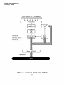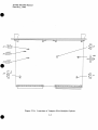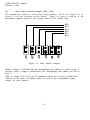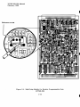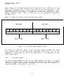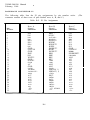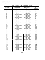
1
 XVME-500 / XVME-590
Analog Input Modules with Channel Options
USER’S MANUAL
ACROMAG INCORPORATED
30765 South Wixom Road
P.O. BOX 437
Wixom, MI 48393-7037 U.S.A.
Tel: (248) 295-0885
Fax: (248) 624-9234
Email: [email protected]
Copyright 2012, Acromag, Inc., Printed in the USA.
Data and specifications are subject to change without notice.
8500-971B XVME-500/590 Manual
February, 1988
Chapter 1
MODULE DESCRIPTION
1.1
INTRODUCTION
The XVME-500 and XVME-590 are Analog Input VMEbus-compatible boards. The
XVME-500 is a single-high (3U), single-wide module, and the XVME-590 is a doublehigh (6U), single-wide module. These two modules are capable of performing
analog-to-digital conversions with 12-bit resolution.
These modules provide 16
single-ended (SE), or 8 differential input (DI) analog input channels.
Adding an XVME-910 channel expansion kit allows analog input expansion to 32 SE
and 16 DI channels. See Appendix A for XVME-910 specifications.
The XVME-500 and XVME-590 modules are available in any of three different
versions:
*
1)
XVME-500/ 1 and XVME-590/ 1 - fixed gain amplifier with 25uSec
conversion time*
2)
XVME-500/2 and XVME-590/2 - programmable gain amp with 25uSec
conversion*
3)
XVME-500/3 and XVME-590/3 - programmable gain amp with 10uSec
conversion*
See Table l-l, Section 1.3 for additional information on conversion time,
settling time and throughput frequency for each version.
1.2 MANUAL STRUCTURE
The first chapter is an overview introducing the user to the XVME-500 and XVME590 general specifications and functional capabilities. Successive chapters develop
the various aspects of module specification and operation in the following manner:
Chapter One - A general discussion of the three Analog Input Module versions,
including complete functional and environmental specifications, VMEbus
compliance information, and detailed block diagrams.
Chapter Two - Module installation information covering specific system
requirements, jumpers and connector pinouts.
Chapter Three - Information required to program the module for analog input
operations.
Chapter Four - Procedures for analog input module calibration.
1-1
XVME-500/590 Manual
February, 1988
Appendices - The Appendices are designed to provide additional information in
terms of the XVME-9 10 channel expansion kit; backplane signal/pin
descriptions; block diagram, assembly illustration and schematics; and a quick
reference section.
1.3 MODULE OPERATIONAL DESCRIPTION
Figure l-1 shows the operational block diagram of the XVME-500 and Figure 1-2
shows the operational block diagram of the XVME-590 Analog Input Module.
1-2
XVME-500/590 Manual
February, 1988
1.3.1
Application
Circuitry
As the previous block diagrams show, the analog-to-digital circuitry in the XVME500 or XVME-590 consists of the following parts:
VMEbus interface circuitry
Fixed gain amplifier (version 1 only)
Programmable gain amplifier (versions 2 & 3 only)
32-element RAM buffer to hold and separate gain value for up to 32
analog inputs (versions 2 & 3 only)
12-bit resolution analog-to-digital converter with input ranges of
+5V, +lOV or O-10 volts
Two eight-channel multiplexers allowing up to 16 SE or 8 DI
signals to be connected to the ADC (expansion kit allows double
signal input); directed by software to select one channel for data
conversion
Resistor programmable gain with addition of a resistor and a
potentiometer
1.3.2
General Operation
As stated before, there are three different versions that the XVME-500 and XVME590 are available in and they are:
XVME-500/ 1
XVME-500/2
XVME-590/3
XVME-590/l
XVME-590/2
XVME-590/3
On all versions, the analog input channels can be configured for bipolar or unipolar
operations. The unipolar range is O-10 volts. The bipolar ranges include 25V and
lfil ov.
Gain capabilities, conversion speeds and throughput frequencies vary with each
version, as displayed in Table 1-l.
1-5
XVME-500/590 Manual
February, 1988
Table l-l
Versions
Version
Conversion
Time
Settling Time
Throughput
XVME-500/ 1
XVME-590/ 1
25uSec
25uSec
25uSec
25uSec
20KHz
20KHz
XVME-500/2
XVME-590/2
25uSec
25uSec
10 uSec
10uSec
28.5KHz
28.5KHz
XVME-500/3
XVME-590/3
10uSec
10uSec
10uSec
10uSec
50KHz
50KHz
1
Frequency
.
Two types of differential amplifiers are available: fixed gain (version 1 of both
modules) and programmable gain (version 2 & 3 of both modules).
The fixed-gain amp offers jumper-selectable gains of xl, x10, xl00 and x1000. In
addition, the fixed-gain amp may offer resistor-programmable gain (to any number
between 1 and 1000) if a resistor (Rl0) and potentiometer (R13) are added (see
Section 2.6.4.3).
The programmable amplifier provides three ranges of jumper-selectable programmable
gains (see Section 2.6.4.-l). Range 1: xl, x2, x5 and x10. Range 2: x4, x8, x20
and x40. Range 3: x10, x20, x50 and x100. A 32-element RAM buffer is provided
with the programmable amps to hold separate gain values for the 32 analog inputs.
Within each range, the four options are software-programmable.
XYCOM’s XVME-500 and XVME-590 are designed to be addressed within the VMEbus
defined 64K Short I/O Address Space. The module address is jumper-selectable to
any of the sixty-four 1K boundaries within the Short I/O Address Space. There are
three 8-bit registers which are used for channel status, control-setting interrupt
vector, programmable gains (versions 2 & 3 on both modules) and channel selection.
In addition, there is a 16-bit data register for reading converted digital data.
1.4
SPECIFICATIONS
The following table lists the electrical, environmental, and VMEbus compliance
specifications for the XVME-500 and XVME-590 Analog Input Modules:
1-6
XVME-500/590 Manual
February, 1988
Table 1-2
XVME-500 and XVME-590 Analog Input Module Specifications
Specification
. Characteristic
Number of Channels
16 (32 optional)
8 (16 optional)
Single-ended
Differential
+5 VDC, ~5%
Supply Voltage
Supply Current
1.90 A
1.60 A
Maximum
Typical
Accuracy
12 bits
+0.5 LSB
50.5 LSB
Guaranteed*
Resolution
Linearity
Differential Linearity
Monotonicity
System Accuracy
+0.0l% FSR, max.
+0.l% FSR, max.
+ 0 1% FSR, max.
Gain = 1
Gain = 10
Gain = 100
System Accuracy Temperature Drift
40 ppm/Degree C, max.
75 ppm/Degree C, max.
110 ppm/Degree C, max.
Gain = 1
Gain = 10
Gain = 1 0 0
60db min.
Common Mode Rejection Ratio
Analog-to-Digital Input (Gain = 1)
Full Scale Voltage Ranges
0-10V
+5v, +lOV
Unipolar
Bipolar
1-7
XVME-500/590 Manual
February, 1988
Table 1-2 (cont’d)
Characteristic
Specification
Programmable Gain (versions 2 & 3)
1, 2, 5, or 10
4, 8, 20 or 40
10, 20, 50, or 100
Range 1
Range 2
Range 3
Fixed Gain (version 3)
Resistor
xl, x10, x100, xl000
programmable
Maximum Input Voltage
+35v
+2ov
Power on
Power off
Input
Impedance
w 1OM ohm resistor
w/o 1OM ohm resistor
1OM ohm min.
1OOM ohm min.
Bias Current
+ 1 OOnA max.
Input
1 OOpf max.
Capacitance
14v
Operating Common Mode Voltage
Speed
Conversion Time
versions 1 & 2
version 3
12-bit
25uSec
10uSec
8-bit
17uSec
6.8uSec
Throughput
version 1
version 2
version 3
20KHz
28.5KHz
50KHz
23.8KHz
37KHz
59.5KHz
Settling Time
version 1
versions 2 & 3
25uSec
10uSec
25uSec
10uSec
External
10 or 20uSec
10, 25uSec
Frequency
Trigger-to-Sample
1-8
XVME-500/590 Manual
February, 1988
Table l-2 (cont’d)
Characteristic
Specification
Environmental Specifications
Temperature
Operating
Non-operating
O” to 65O C
-4OO to 85O C
Humidity
Operating
5 to 95% RH noncondensing
Shock
Operating
30g peak acceleration
11 mSec duration
Non-operating
50g peak acceleration
11 mSec duration
Vibration
Operating
5 to 2000Hz
.015 in. peak-to-peak
2.5g max
Non-operating
5 to 2OOOHz
.030 in. peak-to-peak
5.Og max
VMEbus
Compliance
0
Complies with VMEbus specification Revision C.l
0
A16:D16/D08(EO) DTB Slave
l
Interrupter - I(1) - 1(7)(STAT), ROAK
0
Interrupter Vector - D08(0)
a
Form Factor - SINGLE (XVME-500)
0
Form Factor - DOUBLE (XVME-590)
(DYN)
l-9
XVME-500/590 Manual
February, 1988
XVME-540
Compatibility
All address locations for analog input are identical
0
All bit definitions for registers are the same EXCEPT there are no
LEDs
Channel register/counter now receives
reset; the 540 powers-up ra ndom
l
No fast convert in single channel mode
l-10
reset
software
power-up
XVME-500/590 Manual
February, 1988
Chapter 2
INSTALLATION
2.1 GENERAL
This chapter provides the information needed to configure and install the Analog
Input Module.
2.2
SYSTEM
REQUIREMENTS
The XVME-500 Analog Input Module is single-height (3U), and the XVME-590 is a
double-height (6U) VMEbus-compatible module. To operate, it must be properly
installed in a VMEbus backplane cardcage. The minimum system requirements for
operation of the module are one of the following:
A)
A host processor installed in the same backplane
A properly installed controller subsystem.
An example of such a
subsystem is the XYCOM XVME-010 System Resource Module.
B)
2.3
A host processor which incorporates an on-board controller subsystem
(such as the XVME-600 68000 Processing Module).
LOCATION OF COMPONENTS RELEVANT TO INSTALLATION
The jumpers, calibration potentiometers and connectors on the XVME-500 are
illustrated in Figure 2-1. Figure 2-1A shows the XVME-500 jumpers which have
multiple options.
Figure 2-2 shows the jumpers, calibration potentiometers and
connectors on the XVME-590. Figure 2-2A shows the XVME-590 jumpers which
have multiple options.
2-1
XVME-500/590 Manual
February, 1988
2.4 JUMPERS
Prior to installing the XVME-500 or XVME-590 module, several jumper options must
be configured. The configurations of the jumpers are dependent upon the tab
option and module capabilities required for the application. The jumper options can
be divided into two categories:
0
0
VMEbus Options, and
Analog-to-Digital (A/D) Conversion Options
Table 2-I lists the various jumpers and their uses.
Table 2-1. XVME-500/590 Jumpers
1
VMEbus OPTIONS
Jumpers
Use
Jl0,Jll,J12
Interrupt level select for any interrupts generated by
the module (See Section 2.5.3)
J26,J27,J28,J29
J30,J31
Module base address select jumpers
Section 2.5.1)
J13
This jumper allows module to respond to supervisory
access only (when installed) or to both supervisory
and non-privileged access when removed. (see Section
2.5.2)
Analog-to-Digital
Jumpers
Conversion
(refer to
OPTIONS
Use
These jumpers provide the option of converting
analog inputs to either a two’s complement, straight
binary or offset binary format (see Section 2.6.1)
J2A
Selects 12-bit conversions for analog-to-digital
converter (see Section 2.6.4.4)
J2B
Selects 8-bit conversions for
converter (see Section 2.6.4.4)
analog-to-digital
These jumpers are used to configure inputs for either
bipolar or unipolar input voltages and ranges (see
Section 2.6.3)
2-6
XVME-500/590 Manual
February, 1988
Table 2-l. XVME-500/590 Jumpers (cont’d)
J6,J8,J9
Selects fixed-gain amplification factor on version 1
ONLY (see Section 2.6.4.2)
J7
Used only for modifying version 1 for resistor
programmable gain (see Section 2.6.4.3)
J14,J15,J16,Jl8,
J19,J20
This jumper configuration controls gain ranges for
programmable gain amplifier (versions 2 & 3) (see
Section 2.6.4.1)
J17
This jumper is installed to provide ground reference
for external trigger; J2 1 must be removed if this
option is used (see Section 2.6.4.5)
J21A,J21B,J21C,J21D,
J25
These jumpers are used together to determine if the
inputs will be configured as either 8 differential,
16 single-ended or 16 pseudo-differential input
channels (see Section 2.6.2)
J22A,J22B,J22C,
J22D
Each jumper is used to determine settling times for
the appropriate module amplifier (see Section 3.4.1)
J23,J24
These two jumpers are provided to allow grounding
of an input channel in either the single-ended or the
differential input mode of operation for purposes of
calibration (see Section 2.6.5)
J32 (XVME-590 Only)
2.5
VMEbus
Connects Analog to Digital GND. J32 is jumpered
foil and can be cut if the user desires.
in
OPTIONS
The XVME-500/590 is designed to be addressed within the VMEbus Short I/O
Memory Space. Since each module connected to the bus must have its own unique
base address, the base-addressing scheme for XVME input modules has been designed
to be jumper-selectable. When the XVME-500/590 is installed into the system, it
will occupy a lK-byte block of Short I/O Memory Space.
The XYCOM base address decoding scheme for input modules is such that the
starting address for a module will always reside on a 1K boundary. Thus, the
module base address may be set for any one of 64 possible 1K boundaries within the
Short I/O Address Space.
2-7
XVME-500/590 Manual
February, 1988
2.5.1
Base Address Selection Jumpers (526 - 531)
The module base address is selected by using jumpers J26-J31 (see Figure 2-1 or
Figure 2-2 for the locations on the board). Figure 2-3 shows a close-up of the
base-address jumpers and how each jumper relates to the address lines.
A15
Al4
Al3
Al2
All
A10
l
co
.)
Figure 2-3. Base Address Jumpers
When a jumper is INSTALLED, the corresponding base address bit will be logic ‘0’.
However, when a jumper is REMOVED, the corresponding base address bit will be
logic ‘1’.
Table 2-2 shows a list of the 64 1K boundaries which can be used as module base
addresses in the Short I/O Address Space (as well as the corresponding jumper
settings for each address).
2-8
XVME-500/590 Manual
February, 1988
Supervisor/Non-Privileged Mode Selection (J13)
’ 2.5.2
The XVME-500/590 can be configured to respond only to Supervisory accesses, OR
to both Supervisory and Non-Privileged accesses. The key is the installation or
removal of jumper J13. Table 2-3 shows access options controlled by J13.
Table 2-3. Access Options
Jumper
J13
Access Mode Selection
Address Modifier Code
Installed
Supervisory
2DH
Removed
Supervisory or Non-Privileged
Only
2DH or 29H
VMEbus Interrupt Options (Jl0, Jll, 512)
2.5.3
Three interrupt jumpers (JI0, Jll, 512) select which VMEbus interrupt level is to be
used by the module. The input module can be programmed to generate an interrupt
at the completion of a conversion. These jumpers determine the level of that
interrupt. Interrupt-level jumper options are defined in Table 2-4.
In order to enable interrupts, a bit in the Status/Control register must be set (See
programming chapter Section 3.3.1). Interrupt reset occurs during the interruptacknowledge (IACK*) cycle. A read from the lower byte of the analog-to-digital
conversion register, or a command to start another conversion, will reset the
interrupt bit. Interrupts are also reset during a power-up sequence or when a
software reset is issued (See Table 2-4).
Table 2-4. Interrupt Level Jumpers
Jumpers
Jl0
Jll
0
0
0
0
0
1
1
0
0
1
1
0
1
1
1
1
J12
0
1
0
1
0
1
0
1
VMEbus Interrupt Level
Interrupts Disabled
1
2
3
4
5
6
7
NOTE: IN = LOGIC 0; OUT = LOGIC 1
2-10
XVME-500/590 Manual
February, 1988
2.6
ANALOG-TO-DIGITAL (A/D) CONVERSION OPTIONS
Input Conversion Format Jumpers (Jl, J4)
2.6.1
This jumper option is used to configure A/D conversion circuitry to convert analog
information to one of three formats: straight binary (unipolar); off set binary
(bipolar); or two’s complement binary (bipolar).
Use of this option is dependent upon the data format required by the input control
program employed by the user. This option is inclusive to all input channels and
cannot be utilized on an individual channel basis (see Section 3.3.4.1).
The digital-data format at the A/D converters may be changed (via jumpers) to
accommodate several types of data encoding.
Table 2-5 shows which jumpers
control the data formats for the two different voltage modes.
Table 2-5. Input Conversion Format Jumpers
.
Digital Data Conversion
Format ( All Inputs)
Jumpers
Installed
Input
Mode
Analog to Straight Binary
Analog to Offset Binary
Analog to Two’s Complement
JlA, J4A
JlA, J4A
JlB, J4B
Unipolar
Bipolar
Bipolar
2.6.2
Differential,
Pseudo-Differential/Single-Ended
Input
Option
Jumpers
(Analog Multiplexers) (J21, J25)
The XVME-500/590 can be configured to provide any one of three types of channel
modes in set numbers (see Table 2-6 for input selection jumper options) They are:
1)
16 single-ended (SE) input channels, or
2)
8 differential (DI) input channels, or
3)
16 pseudo-differential (PDI) input channels (allows module to simulate
advantages of true differential with some degradation)
The three modes are mutually exclusive so the module will only accept all SE, or all
DI, or all PDI inputs. It will not accept combinations of the three.
2-11
XVME-500/590 Manual
February, 1988
NOTE
Only one of the three jumper configurations may be
installed at any one time. Make sure that:
1) If the board is to be used in the SE input mode,
the jumpers for DI and PDI operation must be
removed; 2) If the board is to be used in the DI
input mode, the jumpers for SE and PDI operation
must be removed; and 3) If the board is to be used
in the PDI input mode, the jumpers for SE and DI
operation must be removed.
The pseudo-differential option allows 16 input channels, as does the single-ended
option. Unlike the SE channel, the PDI mode uses a common analog ground (pin
JKl-49) to simulate true differential input (Important, see Section 2.6.4.5).
Addition of the XVME-910 (see Appendix A) increases the number of analog
multiplexers from two to four. As a result, the number of available input channels
doubles as follows: SE and PDI increase to 32; DI increases to 16.
Table
2-6.
Single-Ended/Differential,
Jumpers Set
Pseudo-Differential
Jumper
Options
Input Mode
J21A,J21C,J25
Set in this manner, the module inputs
are configured for single-ended operation.
J21B
In this manner,the module inputs are
configured for differential operation.
J21A,J21D,J25
This combination of jumpers configures
the module for pseudo-differential operation.
In addition to the SE/D1 jumpers mentioned, two other jumpers are provided to
allow grounding of an input channel (in either the SE or DI mode). This is done to
allow software to automatically correct any drift in the ADC offset adjustment. In
the SE mode, J23 (Channel 0) or J24 (Channel 8) may be inserted. In the differential mode, both J23 and J24 (Channel 0) must be inserted.
2.6.3
Input Voltage Type and Voltage Range Selection (J3, J5)
The analog inputs may be configured to accept either unipolar or bipolar full-scale
input voltages. Jumpers J3 and J5 determine which voltage type the module will
accept.
2-12
XVME-500/590 Manual
February, 1988
The analog input channels can be jumper-configured to accept voltages in any one
of three ranges. There are two bipolar ranges and one unipolar range.
Bipolar Ranges
Unioolar
+5v
0 to 10V
Range
$ov
The 5 V (bipolar) and 0-10V (unipolar) ranges are selected by jumper J3A. Jumper
J3B selects the &lOV bipolar range. Table 2-7 shows the options.
Table 2-7. Voltage Type and Voltage Range Selection Options
Input Range
Install
Remove
J3A, J5A
J3B, J5B
J3A, J5B
J3B, J5B
J3B, J5A
J3A, J5A
Unipolar:
0-10V
I
Bipolar:
+5v
IlOV
2.6.4
INPUT GAIN RANGE SELECTION
2.6.4.1
Programmable Gain Selection (XVME-500/590-2, XVME-500/590-3)
(J15 & J19; J14 & J18; J16 & J20)
The gain for each input channel is individually programmable over any one of three
possible gain ranges. First, the required range is selected by configuring one of
three pairs of jumpers (J15 & J19; J14 & J18; or J16 & J20). Next, the specific
gains (within the selected range) are determined by the user and written to onboard Gain RAM during an input initialization procedure (See Section 3.3.3).
Thereafter, any time an input is converted (analog-to-digital), it will automatically
apply the gain factor for which it was previously programmed.
The three input
gain ranges are:
Three Input Gain Ranges
Range 1:
1, 2, 5, or 10
Range 2:
4, 8, 20, or 40
Range 3:
10, 20, 50, or 100
2-13
XVME-500/590 Manual
February, 1988
The various input gains are selected by installing two jumpers for each option.
Table 2-8 shows the options and corresponding jumpers.
Table 2-8. Input Gain Range Selection Jumpers
(versions 2 & 3 only)
I
Jumpers
Installed
Gain Range Selected
J15, J19
Range 1
J14, J18
Range 2
J16, J20
Range 3
Only one range can be selected at a time.
The input channels can only be
programmed for specific gains within the selected range.
2.6.4.2
Fixed Gains (Jumper-Selectable - version 1 only)(J6, J7, J8, or J9)
The fixed gain for each analog input channel in the version 1 of the XVME-500/590
is selected by installing or removing one of several jumpers (J6, J7, J8, or J9).
Gains can be selected from one of four different levels as follows:
Level
Gain Selected
I (Unity Gain)
xl
2
x10
3
xl00
4
xl000
Only one gain factor can be selected at a time. The input channels can only be
programmed for a specific gain range. Thus, when a jumper is installed to achieve
a particular gain, others must be removed. Table 2.9 shows which jumpers are used
to select which gains.
2-14
XVh4&500/590 Manual
February, 1988
Table 2-9. Jumpers Selecting Fixed Gains
Gain Selected
2.6.4.3
Jumper
Installed
Jumpers Removed
xl
None
J6, J7, J8, J9
x10
J9
J6, J7, J8
xl00
J8
xl000
J6
J6, J7, J9
.
J7, J8, J9
Resistor-Programmable Gains (version 1 only)
The resistor-programmable gains option increases the versatility of the XVME500/590-l. In order to utilize these gains, it is necessary to install:
1)
A fixed-value resistor (value determined by equation following)
2)
A potentiometer (for fine adjustment of the gain), and
3)
A cut on the printed circuit board.
Installing Resistors To Modify Fixed Gain
(Procedure)
1)
Remove power from the module.
2)
Remove module from the cardcage.
3)
Locate the circuit trace in Figure 2-4.
trace for the XVME-590/l).
2-15
Figure 2-4A shows the circuit
XVME-500/590 Manual
February, 1988
4)
Use a sharp tool (knife, X-acto blade, etc) to sever the trace, as shown
in Figure 2-4 (or Figure 2-4A for the XVME-590).
5)
Use the following formula to calculate the values of ‘Rl0’ and ‘R13’:
Rg = 40K / G - 1
G = desired gain (any number between 1 and 1000)
Example: Determining adjustment to R13 necessary to get a gain of 8.
By using the formula, and assigning ‘G’ the desired value of
‘8’ , Rg is calculated to be 5714 ohms:
G=8
Rl0 = 5.1K (standard value)
R13 = 1K (adjusted to 614 ohms)
Rg = (40K / 8 - 1) = (40,000 / 7) = 5714
Rg is also equal to the sum of values ‘Rl0’ and ‘R13’ (Rl0 + R13). The
standard value of ‘Rl0’ is 5.1K, and that of ‘R13’ is 1K. Because the sum
of these to standard values is 6.1K (6100), ‘R13’ must be adjusted from
1K to 614K (614) to achieve the desired value.
NOTE
The resistor used should be type RN-55E, with a
temperature coefficient of 25/ppm/Degree C, max.
6)
7)
The resistor ‘RI0’ should be soldered in the position designated by the
silkscreen (see Figure 2-4 or Figure 2-4A).
Potentiometer
‘R13’ can be either a BECKMAN (Model 66W) or an
ALLEN-BRADLEY (Model 85W). Carefully solder the potentiometer on the
I PCB as shown in Figure 2-1A or Figure 2-2A (Note the reference to the
adjustment screw in that figure).
8)
Remove jumpers J6, J8 and J9 (if any are in place).
9)
Install jumper J7.
10)
Re-install the module in the cardcage and perform the input calibration
procedure (outlined in Chapter 4, Section 4.2).
11) Once the module is calibrated, the gain may be fine-tuned by monitoring
the voltage at TPl (a ground) and TP2 with a DVM, while adjusting
potentiometer ‘R13’.
2-18
XVME-500/590 Manual
February, 1988
2.6.4.4
Conversion Resolution (J2A, J2B)
A jumper has been provided to change the ADC to an eight-bit converter. This will
allow a faster conversion (if required by the user), but will decrease conversion
resolution.
If this option is chosen, the lower 4 data bits will have to be masked
by software. Table 2-10 shows the conversion resolution jumpers.
Table 2-10.
I
Conversion
Conversion Resolution Jumpers
I
Desired
Jumper
Installed
12-bit
J2A
8-bit
J2B
1
Figure 2-5 shows the various formats of the data input register when either J2A
J2B are installed.
High Byte
015
014
013
012
DII
or
Low Byte
DIO
D9
08
d7
D6
D5
04
03
02
DI
DO
I
I
I
Base + 86H
Base + 87H
J2A 12-bit r e s o l u t i o n ( b y t e s D I I - D O )
J2B 8-bit
resolution
(D11-D4)
(D3-D0 i g n o r e d
by software)
Figure 2-5. How Jumpers Change the Data Register
2-19
XVME-500/590 Manual
February, 1988
2.6.4.5
External Trigger Selection (J 17)
Jumper J17 is installed for external trigger usage. When installed, pin-49 (of
connector JK1) becomes logic ground reference. If J17 is used for an external
trigger option, J21D should not be used. When J17 is removed, pin-49 uses J21 as
common analog ground for pseudo-differential (PDI) mode. If both PDI and an
external trigger are desired, do not use J17. Find a logic ground for external
trigger elsewhere on the module.
2.6.5
Input Calibration Grounding Jumpers (523, 524)
These jumpers are used to ground a single input channel in either the SE or DI
mode for purposes of programmable gain offset adjustment (calibration). If the
inputs are configured for single-ended operation, inserting jumper J23 shorts input
channel 8 to ground. Inserting J24 shorts channel 0 to ground. In differential mode,
inserting both J23 (channel 0 Hi) and J24 (channel 0 Lo) will short channel 0 to
ground.
Table 2-11 shows the relationship between the jumpers and the grounded channels.
Refer to Chapter 4 (Calibration) for exact input calibration procedure.
Table 2-11. Input Calibration Grounding Jumpers
Jumpers
I
2.7
2.7.1
J23 & J24
CONNECTOR
Input Configuration
Channel Sorted to Ground
Single-ended (SE)
Channel 8
Single-ended (PDI)
Channel 0
Differential
Channel 0
PIN ASSIGNMENTS
Connector JKl (XVME-500
Only)
The analog input channels are accessible on the front panel of the module via the
single mass termination header labeled, JKl. Connector JKl is a 50-pin header used
to input analog signals. Its pin-out is compatible with the Analog Devices 3B series
Universal Signal Conditioning System. Table 2-12 defines JKl’s pin-out.
2-20
XVME-500/590 Manual
February, 1988
Table 2-12. Input Connector JKl
Flat Cable
Conductor
1
2
3
4
5
6
7
8
9
10
11
12
13
14
15
16
17
18
19
20
21
22 .
23
24
25
26
27
28
29
30
31
32
33
34
35
36
37
38
.
.
Single-Ended
Configuration
Differential
Configuration
CH. 0
CH. 8
ANALOG
CH. 9
CH. 1
ANALOG
CH. 2
CH. 10
ANALOG
CH. 11
CH. 3
ANALOG
CH. 4
CH. 12
ANALOG
CH. 13
CH. 5
ANALOG
CH. 6
CH. 14
ANALOG
CH. 15
CH. 7
ANALOG
CH. 16’
CH. 24*
ANALOG
CH. 25”
CH. 17”
ANALOG
CH. 18”
CH. 26*
ANALOG
CH. 27*
CH. 19*
ANALOG
CH. 20”
CH.. 28*
CH. 0 LO
CH. 0 HI
ANALOG GND
CH. 1 HI
CH. 1 LO
ANALOG GND
CH. 2 LO
CH. 2 HI
ANALOG GND
CH. 3 HI
CH. 3 LO
ANALOG GND
CH. 4 LO
CH. 4 HI
ANALOG GND
CH. 5 HI
CH. 5 LO
ANALOG GND
CH. 6 LO
CH. 6 HI
ANALOG GND
CH. 7 HI
CH. 7 LO
ANALOG GND
CH. 8 LO*
CH. 8 HI*
ANALOG GND
CH. 9 HI*
CH. 9 LO*
ANALOG GND
CH. 10 LO*
CH. 10 HI*
ANALOG GND
CH. 11 HI*
CH. 11 LO*
ANALOG GND
CH. 12 LO*
CH. 12 HI*
GND
GND
GND
GND
GND
GND
GND
GND
GND
GND
GND
GND
* Those channels marked by (*) are only available after an XVME-9 10 channel
expansion kit is installed. (Table continued next page.)
2-21
XVME-500/590 Manual
February, 1988
Table 2-12. Input Connector JKI (cont’d)
Flat Cable
Conductor
39
40
41
42
43
44
45
Single-Ended
Configuration
Differential
Configuration
ANALOG GND
CH. 29*
CH. 21*
ANALOG GND
CH. 22*
ANALOG GND
CH. 13 HI*
CH. 13 LO*
ANALOG GND
CH. 14 LO*
CH. 14 HI*
ANALOG GND
CH. 15 HI*
CH. 15 LO*
ANALOG GND
POWER GND/PD GND
EXT TRIGGER
CH. 30*
ANALOG GND
CH. 31*
CH. 23*
46
47
48
ANALOG GND
49
POWER GND/PD GND
EXT TRIGGER
50
* Those channels marked by (*) are only available after an XVME-910 channel
expansion kit is installed.
2.7.2
Pl
Connectors
Connectors Pl and P2 are mounted at the rear edge of the board (see Figure 2-1 or
Figure 2-2). The pin connections for Pl (a 96-pin, 3-row connector) contains the
standard address, data, and control signals necessary for the operation of VMEbusdefined NEXP modules. (The signal definitions and pin-outs for the connector are
found in Appendix A of this manual). The Pl connector is designed to mechanically
interface with a VMEbus defined Pl backplane.
2.7.3
P2 Connector (XVME-590 Only)
The P2 connector is a standard VMEbus P2 backplane connector with 96-pins (3
rows). (The pin-outs for the connector P2 are found in Appendix A of this
manual.) The P2 connector is designed to interface with a VMEbus defined P2
backplane. The P2 connector for the XVME-590 will accept the input analog signals
via the user defined VMEbus pins on rows A and C (see Table 2-13).
2-22
XVME-500/590 Manual
February, 1988
Table 2-13. P2’s - JKl Compatibility Pin-out
Flat Cable
Conductor
1
2
3
4
5
6
7
8
9
10
11
12
13
14
15
16
17
18
19
20
21
22
23
24
25
26
27
28
29
30
31
32
33
34
35
36
37
38
39
40
41
42
43
44
45
Single-Ended
Configuration
CH. 0
CH. 8
ANALOG GND
CH. 9
CH. 1
ANALOG GND
CH. 2
CH. 10
ANALOG GND
CH. 11
CH. 3
ANALOG GND
CH. 4
CH. 12
ANALOG GND
CH. 13
CH. 5
ANALOG GND
CH. 6
CH. 14
ANALOG GND
CH. 15
CH. 7
ANALOG GND
CH. 16
CH. 24
ANALOG GND
CH. 25
CH. 17
ANALOG
CH. 18
CH. 26
ANALOG
CH. 27
CH. 19
ANALOG
CH. 20
CH. 28
ANALOG
CH. 29
CH. 21
ANALOG
CH. 22
CH. 30
ANALOG
Differential
Configuration
CH. 0 LO
CH. 0 HI
ANALOG GND
CH. 1 HI
CH. 1 LO
ANALOG GND
CH. 2 LO
CH. 2 HI
ANALOG GND
CH. 3 HI
CH. 3 LO
ANALOG GND
CH. 4 LO
CH. 4 HI
ANALOG GND
CH. 5 HI
CH. 5 LO
ANALOG GND
CH. 6 LO
CH. 6 HI
ANALOG GND
CH. 7 HI
CH. 7 LO
ANALOG GND
CH. 8 LO
CH. 8 HI
ANALOG GND
CH. 9 HI
CH. 9 LO
GND
ANALOG GND
CH. 10 LO
CH. 10 HI
GND
GND
GND
GND
GND
ANALOG
CH. 11
CH. 11
ANALOG
CH. 12
CH. 12
ANALOG
CH. 13
CH. 13
ANALOG
CH. 14
CH. 14
ANALOG
GND
HI
LO
GND
LO
HI
GND
HI
LO
GND
LO
HI
GND
P2
Connector
Cl
Al
C2
A2
C3
A3
C4
A4
c5
A5
C6
A6
C7
A7
C8
A8
C9
A9
Cl0
Al0
Cl1
All
Cl2
Al2
Cl3
Al3
Cl4
Al4
Cl5
Al5
Cl6
Al6
Cl7
Al7
Cl8
Al8
Cl9
A19
C20
A20
C21
A21
C22
A22
C23
XVME-500/590 Manual
February, 1988
Table 2-13. P2’s - JKI Compatibility Pin-out (Cont’d)
Flat Cable
Conductor
Single-Ended
Configuration
46
47
48
49
50
Differential
Configuration
CH. 31
CH. 15 HI
CH. 15 LO
CH. 23
ANALOG GND
ANALOG GND
POWER GND/PD GND POWER GND/PD GN
EXT TRIGGER
EXT TRIGGER
P2
onnector
A23
C24
A24
C25
A25
2.8 JUMPER LIST
The following table summarizes all the XVME-500/590 jumpers and their functions.
Table 2-14. XVME-500/590 Jumper List
Jumper
JlA
JlB
J2A
J2B
J3A
J3B
J4A
J4B
J5A
J5B
J6
J7
J8
J9
Jl0
Jll
J12
J13
J14
J15
J16
J18
J19
J20
J17
J21A
J2lB
J21C
J21D
Description
.
Analog-to-binary conversion with J4A
Analog-to-two’s complement conversion with J4B
Allows 12-bit resolution in ADC conversions
Allows 8-bit resolution in ADC conversions
Voltage range selector to ADC; 0-l0V, +5V
Voltage range selector to ADC; +l0V
Analog-to-binary conversion with J1A
Analog-to-two’s complement conversion with J1B
Unipolar voltage range selector
Bipolar voltage range selector
Fixed gain selector (x1000)
Resistor programmable gain selector
Fixed gain selector (x100)
Fixed gain selector (x10)
A3 interrupt level selector
A2 interrupt level selector
Al interrupt level selector
IN = supervisory only; OUT = supervisory or non-privileged
Programmable gain range selector; Range 2 (4, 8, 20, 40)
Programmable gain range selector; Range 1 (1, 2, 5, 10)
Programmable gain range selector; Range 3 (10, 20, 50, 100)
Programmable gain range selector (accompanies J14)
Programmable gain range selector (accompanies J15)
Programmable gain range selector (accompanies J16)
External trigger selector (remove J21A-D;do not use with PDI)
Configures module for SE operation;accompanies J25 & J21C or D
Configures module for DI operation
Configures module for SE operation with J21A & J25
Configures module for PDI operation with J21A & J25
2-24
XVME-500/590 Manual
February, 1988
Table 2-14. XVME-500/590 Jumper List (Cont’d)
Jumper
J22A
J22B
J22C
J22D
J23
J24
J25
J26
J27
J28
J29
J30
J31
J32
2.9
Description
Determines settling time 80uSec for fixed gain x1-100
Determines settling time 10uSec for programmable gain amp
Determines settling time 24uSec for fixed gain x100
Determines settling time 16uSec (not used)
Ground allows auto drift control by software;input calib.
Ground allows auto drift control by software;with J23 for DI
IN = SE mode selected; OUT = DI mode selected
Module-base address-select jumper
Module-base address-select jumper
Module-base address-select jumper
Module-base address-select jumper
Module-base address-select jumper
Module-base address-select jumper
J32 is jumpered in foil to connect analog to
XVME-590 Only.
digital ground. May be cut if user desires.
POTENTIOMETER
LIST
The following table summarizes the potentiometers and their functions (Table 2-15):
Table 2-15. Potentiometers
Resistor No.
R2
R8
R9
RI1
R13
R17
Description
Unipolar offset adjustment; ADC
Bipolar off set adjustment; ADC
Gain adjustment; ADC
’
Input offset adjustment; fixed gain instr. amp (version 1)
Gain adjustment; resistor programmable gain (version 1)
Input offset adjustment; programmable gain (version 2 & 3)
2-25
XVME-500/590 Manual
February, 1988
2.10
MODULE
INSTALLATION
XYCOM XVME modules are designed to comply with all physical and electrical
VMEbus backplane specifications. The XVME-500 Analog Input Module is a singlehigh VMEbus module. As such, it only requires the Pl backplane. The XVME-590
Analog Input Module may use the P2 of the VMEbus backplane.
CAUTION
Never attempt to install or remove any boards before turning
off the power to the bus, and all related external power
supplies.
Prior to installing a module, you should determine and verify
all relevant jumper configurations, and all connections to
external devices or power supplies. (Please check the jumper
, configuration against the diagrams and lists in this manual.)
To install a board in the cardcage, perform the following steps:
1) Make sure the cardcage slot (which will hold the module) is clear and
accessible.
2) Center the board on the plastic guides in the slot (so the handle on the
front panel is towards the bottom of the cardcage).
3) Push the card slowly toward the rear of the chassis, until the connectors
engage (the card should slide freely in the plastic guides).
4) Apply straightforward pressure to the handle on the panel front, until the
connector is fully engaged and properly seated.
2-26
XVME-500/590 Manual
February, 1988
NOTE
It should not be necessary to use excessive force or pressure
to engage the connectors.
If the board does not properly
connect with the backplane, remove the module and inspect all
connectors and guide slots for possible damage or obstructions.
5) Once the board is properly seated, secure it to the chassis by tightening
the two machine screws at the extreme top and bottom of the board.
2.10.1
Installing a 6U Front Panel Kit (XVME-500 Optional)
XYCOM’s XVME-941 is an optional 6U front panel kit designed to replace the
existing 3U front panel on the XVME-500. The 6U front panel facilitates the
secure installation of single-high modules in those chassis which are designed to
accommodate only double-high modules. The following is a step-by-step procedure
for installing the 6U front panel on an XVME-500 module (See Figure 2-6 for a
graphic depiction of the installation procedure).
1) Turn power off.
2) Disconnect the module from the bus.
3) Remove the screw and plastic collar assemblies (labeled 6 & 7) from the
extreme top and bottom of the existing 3U front panel (11).
4) Install the screw assemblies in their corresponding locations on the 6U
front panel.
5) Slide the module identification plate (13) from the handle (9) on the 3U
front panel.
By removing the screw/nut found inside the handle, the
entire assemble will separate from the 3U front panel.
6) Remove the counter-sunk screw (8) to separate the 3U front panel from
the printed circuit board (12).
7) Line-up the plastic support brackets on the printed circuit board with the
corresponding holes in the 6U front panel (i.e., the holes at the top and
top-center of the panel). Install the counter-sunk screw (8) in the hole
near the top-center of the 6U panel, securing it to the lower support
bracket on the printed circuit board.
8) Install the handle assembly (taken from the 3U panel) at the top of the
6U panel, using the screw and nut previously ‘attached inside the handle.
Secure the handle by sliding the I.D. plate into place.
2-27
XVME-500/590 Manual
February, 1988
Chapter 3
PROGRAMMING
3.1
INTRODUCTION
This chapter provides information required to program the XVME-500/590 Analog
Input Module for analog-to-digital signal conversions. The presentation of the
information is as follows:
l
Presentation of the module address map with programming locations
l
Discussion of base addressing and how the conversion registers are
accessed
A/D conversion modes and principals
3.2
BASE
ADDRESSING
The XVME-500/590 Analog Input Module is designed to be addressed within the
VMEbus- defined 64K Short I/O Address Space. When the module is installed in a
system, it will occupy a IK byte block of the Short I/O Address Space. The base
address decoding scheme for the XVME I/O modules positions the starting address
for each board on a 1K boundary. Thus, there are 64 possible base addresses (1K
boundaries) for the XVME-500/590 within the Short I/O Address Space. (Refer to
Section 2.5.1 for the list of base addresses and their corresponding list of jumper
configurations.) ’
The logical registers utilized for the conversion data on the XVME-500/590 are
given specific addresses within the 1K of block-address space occupied by the
module.
These addresses are offset from the module base address. Figure 3-1
shows a representative memory map for the XVME-500/590 module.
3-l
XVME-500/590 Manual
February, 1988
EVEN
ODD
Base + OOH
0lH
UNDEFINED
+ 7EH
7FH
w--w-----
+ 80H --m---s-w
Status/Control
+ 82H --w-------i
Interrupter/Vector
+ 84H
Gain/Channel
+ 86H
A/D High Byte
Reg.
81H
Reg.
Reg.
A/D Low Byte
UNDEFINED
rlgure 3-l. XVME-500/590 Analog Input Module Memory Map
3-2
83H
85H
87H
XVME-500/590 Manual
February, I988
A specific register on the module can be accessed by simply adding the specific
register offset to the module base address. For example, the module Status/Control
Register is located at address 81H within the I/O interface block. Thus, if the
module base address is jumpered to l000H, the Status/Control Register would be
accessible at address 108IH.
(Module base address)
1OOOH
+
(Register offset)
81H
=
(Status/Control
1081H
Reg.)
For memory-mapped CPU modules (such as 68000 CPU modules), the short I/O
address space is memory-mapped to begin at a specific address. For such modules,
the register offset is an offset from the start of this memory-mapped short I/O
address space. For example, if the short I/O address space of a 68000 CPU module
starts at F90000H, and if the base address of the XVME-500/590 . is set at lOOOH,
then the actual module base address would be F91000H.
3.3 INTERFACE BLOCK
Each of the following programming locations of the XVME-500/590 interface block
(previously shown in Figure 3-1) are defined in greater detail in this chapter’s
remaining sections:
Status/Control Register (base + 81H): (Section 3.3.1)
The status/control
register contains eight single-bit locations which provide control signals to
reset the module, enable interrupts, start conversion, show if there are
interrupts pending, and select the mode of analog input operation (i.e., single
channel, sequential channel, random channel and external trigger).
Interrupt Acknowledge (IACK) Vector Register (base + 83H): (Section 3.3.2)
Holds the vector to be driven onto the VMEbus when an interrupt generated
by the input module is acknowledged.
Gain/Channel Register (base + 85H): (Section 3.3.3) This register is used to
initiate random channel conversions, and to program a 32-element input gain
RAM as part of an input initialization procedure. The lower five bits of this
register are used to select one of the input channels for conversion, or gain
programming.
The sixth bit determines whether the register is used to
program gain, or to read the gain and convert a specific channel. The upper
two bits are used to select one of four allowable gain settings to be
programmed for a selected channel.
A/D Input High Byte (base + 86H) and A/D Input Low Byte (base + 87H):
(Section 3.3.4) These locations contain the digital data which results from
A/D conversions.
3-3
XVME-500/590 Manual
February, 1988
3.3.1
Status/Control Register (Base + 8lH)
The status/control register provides the control signals required to reset the
module, enable interrupts, start conversion and select the mode of operation. The
four modes of operation are single, sequential, random channel and external trigger.
Writing to the status/control register can: initiate an A/D conversion, select an A/D
conversion mode, reset the module, and enable module interrupts to the VMEbus.
Reading from the status/control register can indicate: whether or not a conversion
is in progress (or when a conversion is complete), and if there are interrupts
pending. Table 3-1 describes the functions of the status/control bits.
Table 3-1. Status/Control Register
Bit No.
Function
I
Control
Status
0
1
2
3
4
5
6
7
Interrupt Pending
Interrupt Enable
Board Reset
Mode 0
Mode 1
A/D Busy
Status/Control
3.3.1.1
D7
Register
Bit
No Connection .
Interrupt Enable
Board Reset
Mode 0
Mode 1
Convert
Definitions
This bit acts as a ‘busy’ flag, showing when an A/D conversion is in
progress.
A logic ‘1’ at this location indicates the analog input
module is in the process of making a conversion. The level of this
bit should be checked prior to start-up of new conversions, or the
in-progress conversion could be ruined.
Writing a logic ‘1’ to this bit “forces” a conversion to start.
This method of forcing a conversion works in any of the four A/D
data conversion modes.
D6 & 5:
These are read/write bits that describe which of the four analog
modes the module will operate within. Table 3-2 shows the four
input mode options.
3-4
lXVME-500/590
Manual
February, 1988
Table 3-2. Input Mode Options
9
Mode Bits
1
Bit 6
Bit 5
A/D Conversion Mode
0
0
1
1
0
1
0
1
Single Channel
Sequential Channel
Random Channel
External Trigger
Single
Channel
Sequential
Random
Starts conversion process when reading lower 8 bits
Channel
Channel
External Trigger
Channels are converted in a sequence, beginning
with a specific number; starts conversion process
when reading lower 8 bits
Starts conversion after channel number is written
to Gain Channel register (in read mode; see Table
2-6)
Starts conversion on positive trigger signal
received on Pin 50 (ground reference on Pin 49) of
of connector JKl (see Figure 3-6 for timing)
The use of input conversion modes is explained in greater detail in Section 3.4.1
D4
This bit provides a means for a module software reset. If
“toggled” to logic ‘l’, then back to logic ‘0’, a software reset
will occur (in bits D7 and D2)
D3
A logic ‘1’ written to this location will enable the module to
generate VMEbus interrupts (if the associated jumpers are set
appropriately; see Section 2.5.3)
D2
This bit is an ‘interrupt-pending’ flag. Logic ‘1’ at this location
says an A/D conversion has been completed. The interrupt-pending
bit can be cleared in one of three ways:
1)
2)
3)
Causing a new A/D conversion (see bit D7)
Performing backplane or software reset (see bit D4)
Reading the converted input data from the lower order
data byte
Dl & D0: These bits are not used by the XVME-500/590 s t a t u s / c o n t r o l
register.
3-5
XVME-500/590 Manual
February, 1988
3.3.2
Interrupt Acknowledge (IACK) Vector Register (Base + 83H)
The XVME-500/590 is capable of generating an interrupt at the completion of an
A/D conversion at any of the seven levels allowed by the VMEbus specification.
Interrupts are enabled by writing a logic ‘1’ to bit D3 of the status/control register.
The ability to generate module interrupts is dependent upon setting three jumpers
(Jl0, Jll, 512; see Section 2.5.3). The Interrupt Acknowledge Vector Register is a
write-only register. It holds the vector to be driven on the VMEbus when the
interrupt generated by the input module is acknowledged. This register is accessible
at the module base address + 83H.
3.3.3
Gain/Channel Register (Base + 85H)
The XVME-500/590 uses a 32-element on-board Gain RAM to store a gain factor for
each analog input channel. Only two of the three versions of the module are
software-programmable (versions 2 & 3).
The XVME-500/590-l (as displayed in Sections 2.6.4.2 and 2.6.4.3) realizes gains in
one of two non-software methods. The first method is gain selection via jumpers.
This method allows the input channels to be programmed for a specific gain in one
range. The second method allows modifications of the fixed gain via resistor (and
potentiometer)
programming.
This section is devoted entirely to the programming capabilities of the more
versatile XVME-500/590-2 and XVME-500/590-3. In these modules, one of three
gain ranges is selected via jumper-option at the time the module is installed (see
Section 2.6.4.1). For convenience, the gain ranges and factors are repeated in Table
3-3 .
Table 3-3. Input Gain Ranges and Factors
Gain Range
Gain Factors Covered
1, 2, 5 or 10
4, 8, 20 or 40
10, 20, 50 or 100
Initialization
Immediately after power-up or system-reset, the Gain RAM
(initialized) to provide each input channel (16 DI or 32 SE)
factor.
Once an input channel is initialized this way, the
will automatically be applied when any A/D conversion occurs
3-6
should be programmed
with an associated gain
associated gain factor
on that channel.
XVME-500/590 Manual
February, 1988
The Gain RAM is programmed by using the Gain/Channel Register (base + 85H). If
the module is operating in the Random Channel conversion mode (see Section
3.4.1.3) this register may also be used to “force” an A/D conversion start (much like
the function performed by bit D7 of the status/control register). Figure 3-2 shows
how the Gain/Channel register is arranged.
XVME-50012,
50013
I
XVME-500/l
.
D7
D6
05
04
03
02
Dl
DO
.
Selects Gain
00-Gain=1
01-Gain=2
10-Gain=3
11-Gain=4
I
Selects
Channel I
Configures the Register to Program (Iogic“1”)
or to Read/Convert the gain
Figure 3-2. Gain/Channel Register
The first five bits of this register (DO-D4) are used to select one of the input
channels (0 thru 15 for differential; 0 thru 3 1 for single-ended) for channel
conversion or channel gain programming. Table 3-4 lists the channel selection
codes which are used for DI (0-15) and SE (0-31) operation.
3-7
XVME-500/590 Manual
February, 1988
Table 3-4. Channel Selection Codes
Data Bits
Channel
Selected
I
D4
0
0
0
0
0
0
0
0
0
0
0
0
0
0
0
0
1
1
1
1
1
1
1
1
1
1
1
1
1
1
1
1
*
Yi-j-YT
0
0
0
0
0
0
0
0
1
1
1
1
1
1*
1
1
0
0
0
0
0
0
0
0
1
1
1
1
1
1
1
1
0
0
0
0
1
1
1
1
0
0
0
0
1
1
1
1
0
0
0
0
1
1
1
1
0
0
0
0
1
1
1
1
Dl
DO
0
0
1
1
0
0
1
1
0
0
1
1
0
0
I
1
0
0
1
1
0
0
1
1
0
0
1
I
0
0
1
1
0
1
0
1
0
1
0
1
0
1
0
1
0
1
0
1
0
1
0
1
0
1
0
1
0
1
0
1
0
1
0
1
Channel 0
Channel 1
Channel 2
Channel 3
Channel 4
Channel 5
Channel 6
Channel 7
Channel 8
Channel 9
Channel 10
Channel 1I
Channel 12
Channel 13
Channel 14
Channel 15
Channel 16*
Channel 17*
Channel 18*
Channel 19*
Channel 20*
Channel 21*
Channel 22*
Channel 23*
Channel 24*
Channel 25*
Channel 26*
Channel 27*
Channel 28*
Channel 29*
Channel 30*
Channel 31*
Those channels marked by (*) are only available after installation of an XVME910 channel expansion kit.
3-8
XVME-500/590 Manual
February, 1988
Programmable Gain Selection
D7 & D6: The upper two bits of the register (D6 & D7) are used to select one
of four gain factors available in each of the three jumper-selectable
gain ranges (see Table 3-3).
Table 3-5 shows which codes are
written to bits D6 & D7 to select specific gain factors (according to
the gain range previously selected).
Table 3-5. Gain Selection Bits
Gain/Channel Register
Gain Selected
D7
D6
Range 1
Range 2
0
0
1
1
0
1
0
1
1
2
5
10
4
8
20
40
Range 3
10
20
50
100
l
Bit D5:
This sixth bit of the gain/channel register allows the register to be
used to program (initialize) gain RAM, or it allows the register to
be used to read the gain RAM
The specific channel can be programmed to apply the chosen gain
factor any time it converts a signal as follows:
1)
Write logic ‘1’ to bit D5 with a specific channel number
(as in Table 3-5)
2)
Add desired gain factor from the selected gain range
(Table 3-6)
The corresponding gain factor and channel number (previously programmed) can be
read back by reading address base + 85H.
EXAMPLES
Example 1:
Programming Channel 8 For a Gain of Two
By writing 68H to the module base address + 85H, input-channel 8 would be
programmed for an automatic application of a gain factor of 2 when it converts a
signal. (Note logic numbers written beneath bit numbers in Figure 3-3.)
3-9
XVME-500/590 Manual
February, 1988
07
0
Gain Factor
of 2
D6
1
D5
1
04
0
Enables the
Register to
Write* to
Gain RAM
03
1
02
0
01
0
DO
0
Selects Channel
8 for gain
programming
Figure 3-3. Select Channel 8 For Gain
Example 2:
Reading and Initiating a Conversion at Channel 15
By writing OFH to the module base + 85H (in the Random Channel mode), the Gain
RAM for channel 15 can be read (the gain is read at bits D6 & D7). When reading
base + 85H, D5 will always be zero because it is grounded. In addition, a
conversion is initiated on channel 15 (See Figure 3-4).
07
X
1
06
X
05
0
04
0
03
1
‘02
1
01
1
DO
1
I
Gain Factor’
is read here
Enables
Register for
Convert Mode
Selects Channel
15 for a gain
Read /Convert
Figure 3-4. Conversion at Channel 15
3.3.4
A/D Data Input Register (Base + word location 86H)
The A/D converter produces digital data which corresponds to the applied analog
input from a specified channel.
This digital data is accessible to the ‘Host’
processor at the 16-bit A/D Data Input Register (base + 86H). A word register (16b i t ) i s u s e d t o p r o v i d e t h e s p a c e n e c e s s a r y f o r 12-bit resolution.
Digital
information in this register may be read in either a byte or word format.
3-10
XVME-500/590 Manual
February, 1988
When reading the A/D input data, however, the high byte (base + 86H) must be read
before the low byte (base + 87H); or they must be read simultaneously.
This
stipulation is mandatory because a read from the low data byte will initiate a new
A/D conversion if the module is operating in either the sequential or singlechannel conversion mode. Thus, it would write over the information contained in
the higher byte.
Figure 3-5 shows the format of the A/D data input register.
High Byte
D15
D14
D13 D12 Dll
Low Byte
Dl0
D9
D8
D7
Base + 86H
D6
D5
D4
D3
D2
Dl
DO
Base + 87H
Figure 3-5. A/D Data Input Register Format
The manner in which data appears at the A/D Data Register depends upon which
input operation mode has been previously programmed (see Section 3.3.1.1 for the
explanation of status/control bits D5 & D6; and Section 3.4 for information on the
analog input modes).
3.3.4.1
A/D Data Format
The A/D converter digitizes the value of an analog signal on the input of a selected
channel. The digital format of the converted data depends upon which data format
and input voltage mode (unipolar or bipolar) have been previously jumpered at
module installation (see Sections 2.6.1 and 2.6.2).
3-11
XVME-500/590 Manual
February, 1988
NOTE
The LSB (Least Significant Bit) represents the
change in input voltage that results in an increase
or decrease of the binary code by one count. The
LSB is derived from the full range of either current
or voltage (Vfsr), divided by the maximum conversion
resolution (i.e., 12 bits or 4096 in binary counts).
Thus, the value of one LSB can be determined by the
following:
Unipolar LSB = Vfsr
4096
Bipolar LSB = (+Vf sr)-(-Vf sr)
4096
The following list shows the value of l-LSB for each range:
+5v = 2.44 14mV
+1ov = 4.8828mV
0 - 1OV = 2.4414mV
3.4 A/D CONVERSION PRINCIPALS
Any procedure for configuring the Analog Input Module to convert analog inputs to
digital data must include the following elements:
1)
Jumper Configurations (see Chapter 2) Jumpers must be configured for
the desired interrupt level, input type (DI or SE; and bipolar or unipolar),
input voltage range, input gain range and input binary data format
(straight binary, offset binary or two’s complement).
2)
Initialization (see Section 3.3.3)
Gain RAM must be initialized
(programmed) by writing to the gain/channel register.
3)
Calibration (see Chapter 4) Calibrations must be performed at installation
and whenever adjustments are made to change gains and ranges. This
will help to assure accurate conversion of data by the analog input
module.
4)
Conversion Mode Selection (see Sections 3.4.1 and 3.1.1) One of four
A/D conversion modes must be selected by writing to the status/control
register.
5)
Conversion Initiation (see Sections 3.3.3 and 3.4.1) The A/D conversion
process must be initiated. A conversion may be ‘force’ started, initiated
by reading the low order byte of the A/D Data Register in two of the
four modes, or started via External Trigger.
3-14
XVME-500/590 Manual
February, 1988
3.4.1
A/D Conversion Modes
The A/D conversion process can operate in any one of four possible conversion
modes. They are:
MODE
DEFINITION
0
Single Channel Conversion: Repeated A/D conversions are performed
on a specified channel.
1
Sequential Channel Conversion: Channels are converted in sequence
beginning with a specified channel.
2
Random Channel Conversion: A single A/D conversion is performed
on the selected channel.
3
Externally Triggered Conversion: A selected channel will be
converted only when a positive trigger signal (referenced to
logic ground is received on Pin-50 (ground reference on Pin-49)
of connector JKI.
Four conditions may cause a conversion to be initiated. These conditions are:
1)
Writing to the channel/gain register in random channel mode, with data
bit 5 at a logic ‘0’
2)
Reading the low byte from the ADC while in the single or sequential
channel mode
3)
Execution of the convert command
4)
Initiating an external trigger
A jumper-selectable settling time is provided for the two instrumentation amplifiers
and for the amount of time (they) take to settle. Settling times of I0uSec, 16uSec,
24uSec and 80uSec are available.
NOTE
If the programmable gain amp is used, 10uSec
settling is all that needs to be jumpered. The fixedgain amp, however, requires a settling time of 24uSec
for gains of 1 to 100, and 80uSec for a gain of more
than 100.
3-15
XVME-500/590 Manual
February, 1988
SETTLING TIMES for these module amplifier jumpers are as follows:
J22A
J22B
J22C
J22D
- 24uSec
- 10uSec
- 80uSec
- 16uSec (not used)
A conversion mode is selected by writing its corresponding two-bit code to bits D5
and D6 of the status/control register (see Table 3-2 Input Mode Options). The
following subsections define each of the input conversion modes and list the
procedure for using each.
3.4.1.1
Single Channel Mode
In the single-channel mode, the module will automatically start another conversion
on the specified channel, after the low-order A/D input byte (base + 8 1H) has been
read.
Procedure
1)
Write the appropriate control byte to the status/control register (base +
81H). The objective is to set both D5 and D6 to logic ‘0’.
2)
Select the desired channel by writing the channel number to bits D0 thru
Assuming the corD4 of the gain/channel register (base + 85H).
responding Gain RAM was properly initialized (programmed) after powerup, the gain will not have to be rewritten at this time (unless a change
in gain is desired).-
3)
To initiate the first conversion, perform a “dummy” read (base + 87H), or
force a conversion by writing a logic ‘1’ to bit D7 of the status/control
register (make sure the appropriate mode and interrupt states have been
selected).
4)
Wait until the conversion is complete (i.e., check the busy flag (bit D7)
of the status/control register, or use interrupts).
5)
Read the results of the conversion from the A/D input register -- high
byte (base + 86H) before the low byte (base 87H), or a 16-bit read.
After the low byte is read, a new conversion will automatically be
initiated on the same channel.
3-16
XVME-500/590 Manual
February, 1988
3.4.1.2
Sequential Channel Mode
In the sequential-channel mode, the module will automatically increment the channel
by one and initiate a conversion on the next channel (previous channel + 1). This
will occur after the low order A/D input byte (base + 87H) has been read. A
conversion can be initiated in this mode without incrementing the channel number
by writing a logic ‘1’ to bit D7 of the status/control register (by forcing a
conversion).
Procedure
1)
Write a control byte to the status/control register (base + 81H) that sets
bit D5 to logic ‘1’ and bit D6 to logic ‘0’.
2)
Select a starting channel by writing the channel number to bits D0 thru
D4 of the gain/channel register (base + 85H). Assuming that the corresponding Gain RAM was properly initialized (programmed) after powerup, the gain will not have to be rewritten at this time (unless a change
in gain is desired).
3)
To initiate the first conversion, write a control byte to the status/control
register that sets bit D7 to logic ‘1’. This action will force a conversion ’
on the specified starting channel without incrementing the channel
number. Then, by reading the low order A/D data byte (base + 87H), the
channel number will be incremented by one; and the next conversion will
be started.
NOTE
The first conversion may also be initiated by doing a
“dummy” read of the low order A/D input byte. This
method, though, will increment the channel number
written to the Gain/Channel Register in step 2.
When the dummy read method is used to initiate the
first conversion, the channel offset may be corrected
by specifying a channel number (in step 2) which is
one less than the desired starting channel number
(e.g., if the first channel for conversion is channel 0
then channel 31 should be entered as the starting
channel).
4)
Wait until the conversion is complete (i.e., check the busy flag (bit D7)
of the status/control register, or use interrupts).
5)
Read the results of the conversion from the A/D data registers -- high
byte before low byte (base + 86H before base + 87H). After the low byte
is read, a new conversion will automatically be initiated on the next
channel (previous channel + 1).
3-17
XVME-500/590 Manual
February, 1988
3.4.1.3
Random Channel Selection
In the random-channel mode: A control byte written to the gain/channel register
- - which specifies a channel number and sets bit D5 to logic ‘0’ -- will automatically start a conversion on the specified channel.
Procedure
1)
Write a control byte to the status/control register that sets bit D5 to
logic ‘0’, and bit D6 to logic ‘1’.
2)
Select the desired channel and initiate the conversion by writing the
channel number to bits D0 thru D4, and logic ‘0’ to bit D5 of the
gain/channel register. Assuming that the corresponding Gain RAM was
properly initialized (programmed) after power-up, this action will initiate
a conversion with the correct gain on a specified channel. A conversion
may also be forced by using bit D7 of the status/control register.
3)
The result of the conversion can be read from the A/D data registers
(base = 86H - 87H) in either the byte or word format. In the randomchannel mode, the data resulting from a conversion will remain in the
A/D registers until another conversion is initiated.
3.4.1.4
External Trigger Conversion Mode
To access the external-trigger mode, jumper J17 must be installed and jumper J21D
must be removed. This allows the rising edge of a low-going, externally triggered
pulse (on pin 50 of JKl or pin P2C-25 on P2 of XVME-590) -- referenced to logic
ground (pin 49 of JKl or pin P2A-25 on P2 of XVME-590) -- to initiate a
conversion. Figure 3-6 shows the timing constraints.
3-18
XVME-500/590 Manual
February, 1988
Rising edge
triggers
conversion
100 nsec.
minimum
Figure 3-6. External Trigger Pulse
Procedure
1)
Be sure proper jumper alignments are in place. Connect the externaltrigger source to pin 50 of connector JKl, and connect the externaltrigger source-return to pin 49 of connector JKI.
2)
Write a control byte to the status/control register (base + 81H)
bits D5 and D6 to logic ‘1’.
3)
Select the desired channel by writing the channel number to bits D0 thru
D4 of the gain/channel register. Assuming that the Gain RAM was
properly initialized (programmed) after power-up, it will not be necessary
to rewrite the gain at this time (unless a gain change is required).
4)
The selected channel will initiate a conversion on the rising edge of the
external trigger. The conversion results are read from the A/D data
registers. The next conversion will not take place until the next rising
edge of the external trigger, or until a new conversion is forced on the
channel via bit D7 of the status/control register.
3-19
that sets
XVME-500/590 Manual
February, 1988
NOTE
A software reset (see Section 3.3.1.1) will reset the
flip-flop used to latch the external-trigger pulse, and
abort any conversion in progress.
If an external trigger occurs while the module is in any mode other than the
external-trigger mode, the trigger signal will be latched and a conversion will occur
as soon as the external-trigger mode is entered.
3.4.2
Interrupts
The analog input portion of the module can generate an interrupt to notify the host
that the A/D conversion is complete and the results are available. The level and
vector generated by this interrupt are both user-selectable.
The following three steps must be performed in order to generate an interrupt:
1)
Interrupt level select jumpers must be configured to enable the module
IACK* handling circuitry (see Section 2.5.3).
2)
The Interrupt Vector Register (location base + 83H) must be loaded with
the required vector. This vector register will be read by the interrupt
handler when the interrupt is acknowledged.
3)
Interrupts must be enabled via bit D2 in the’status/control register (see
Section 3.3.1.1).
At the completion of a conversion, an interrupt will be generated.
3.4.3
Current Loop Inputs
An A/D input will operate in a 4-20mA or 10-50mA current loop configuration with
the addition of an external current sensing resistor. The current sensing resistor
should be selected to generate a voltage within the predetermined, jumper-selected
voltage range (0-10V max.). A voltage drop of less than IV will provide current of
less than 4mA, and would thus indicate improper operation of the current loop.
Typically, the resistors used would be:
A 500-ohm 1/2W for the 4-20mA configuration,
OR
A 200-ohm 1/2W for the l0-50mA configuration.
3-20
XVME-500/590 Manual
February, 1988
The resistors should be 0.l% tolerance or better, with stable temperature coefficient
characteristics (e.g., 25ppm or better). All input channels operate with the same
full scale input range.
3-21
XVME-500/590 Manual
February, 1988
Chapter 4
INPUT CALIBRATION
4.1 INTRODUCTION
Calibration facilities have been provided on the XVME-500/590 Analog Input Module
for the analog input circuits. It is recommended that any time the module is
reconfigured (i.e. gain jumpers are changed, or new inputs are added etc.) that the
calibration should be checked and adjusted if necessary.
The calibration procedure entails offset and gain adjustment for the input channels
in either the unipolar or the bipolar modes of operation. Table 4-l provides a list
of the potentiometers and their applications for the input circuit calibration.
Relative locations of the calibration potentiometers can be found in Figure 2-1
(XVME-500) or Figure 2-2 (XVME-590).
Table 4-1. A/D Calibration Potentiometers
Resistor
R2
R8
R9
R17
Rll
R13
4.2
Description
ADC
ADC
ADC
Input
Input
Gain
unipolar offset adjust
bipolar offset adjust
gain adjust
offset adjust Prog. Gain (version 2 and 3 only)
Offset for Resis. Prog. Gain (version 1 only)
Adjust for Resis. Prog. Gain (version 1 only)
INPUT CALIBRATION PROCEDURE
4.2.1
Equipment
Required
The following equipment is required to perform input calibration:
1)
A 5-digit volt meter capable of reading +3OuV.
2)
A small flat-bladed screw driver.
3)
A precision voltage source, capable of supplying +lOV with a minimum
resolution of: 1.22mV.
The inputs can be calibrated in either the single-ended or differential configuration.
Calibration begins by offset nulling the instrumentation amplifier (either fixed gain
or programmable depending upon the version of the module) with channel 0 selected
and its inputs grounded.
4-l
XVME-500/590 Manual
February, 1988
4.2.2
Programmable Gain Offset Adjustment (version 2 & 3)
The following adjustments must be made for the input and output stage of the
programmable gain instrumentation amplifier:
1)
Remove any connections at JKl
2)
Set potentiometer R17 to center position. If the module is configured for
differential mode insert jumpers J23 and 24, if the module is in the
single-ended mode insert just jumper J23, and if the module is configured
for Pseudo-differential mode insert jumpers J23 and J17.
3)
Set input to address the first channel (CH0).
4)
Insert jumpers J15, and J19, and set the input stage gain to 1 (by setting
bits D6 and D7 of the Gain/Channel register to logic “0”). Measure and
record the amplifier output voltage (V, ) at TP2 (TPl is ground).
5)
Set the input stage gain to 10 (by setting bits D6 and D7 of the
Gain/Channel register to logic “1”). Measure and record the output
voltage (V, ) at TP2.
6)
Calculate the voltage offset with the following formula:
Voltage Offset (Voos) =
[(10 * v-1
9
7)
While maintaining an input stage gain of 10, adjust the input offset
voltage potentiometer (R17) until the output at TP2 is equal to Voos
(+3OuV).
8)
Reset gain range jumpers to the desired range (see Table 2-6).
9)
Remove grounding jumpers (J23 & J24).
4.2.3
Fixed Gain Offset Adjustment (version 1)
The following adjustments must be made to the input and output stages of the fixed
gain instrumentation amplifier (version 1 only):
1)
Remove any connections at JKl
2)
If the module is configured for differential mode insert jumpers J23 and
24, if the module is in the single-ended mode insert just jumper J23, and
if the module is configured for Pseudo-differential mode insert jumpers
J23 and J17.
4-2
XVME-500/590 Manual
February, 1988
Appendix A
INSTALLING AN XVME-910 CHANNEL EXPANSION KIT
.
(Optional)
A.1 INSTALLATION
The number of analog inputs on the XVME-500/590 can be expanded from 16 singleended/8 differential to 32 single-ended/l6 differential by installing an XVME-910
Channel Expansion Kit. The kit consists of two additional 8 input analog multiplexers. Installation is simply a matter of positioning the two integrated circuits on
the board in locations U19 and U23, and soldering them in place (see Appendix C,
the assembly drawing for the locations of these IC’s).
NOTE
Static precautions should be taken when handling the
chips, and a low-wattage soldering iron (30 watts or
less) should be used.
Care should be taken to make sure pin 1 on the chip
is aligned correctly.
A-l
XVME-500/590 Manual
February, 1988
Appendix B
* VMEbus CONNECTOR/PIN DESCRIPTION
The XVME-500 and XVME-590 Modules are VMEbus compatible boards. There is
one 96-pin bus connector on the rear edge of the board labeled Pl (refer to
Chapter 2, Figure 2-1 for the location) and the XVME-590 also uses the P2
connector. The signals carried by connector PI are the standard address, data, and
control signals required for a PI backplane interface, as defined by the VMEbus
specification.
Table B-l identifies and defines the signals carried by the Pl
connector. Table B-3 shows the pin-outs for the P2 connector.
Table B-l. Pl - VMEbus Signal Identification
Signal
Mnemonic
Connector
and
Pin Number
ACFAIL*
lB:3
.
Signal Name and Description
AC FAILURE: Open-collectors driven signal which
indicates that the AC input to the power supply is no
longer being provided, or that the required input
voltage levels are not being met.
IACKIN*
IA:21
INTERRUPT ACKNOWLEDGE IN: Totem-pole driven
signal. IACKIN* and IACKOUT* signals form a daisychained acknowledge. The IACKIN* signal indicates to
the VME board that an acknowledge cycle is in
progress.
IACKOUT*
1A:22
INTERRUPT ACKNOWLEDGE OUT: Totem-pole driven
signal. IACKIN* and IACKOUT* signals form a daisychained acknowledge. The IACKOUT* signal indicates
to the next board that an acknowledge cycle is in
progress.
AMO-AM5
1A:23
lB:16,17,
18,19
lC:14
ADDRESS MODIFIER (bits O-5): Three-state driven
lines that provide additional information about the
address bus, such as: size, cycle type, and/or DTB
master
identification.
AS*
lA:18
ADDRESS STROBE: Three-state driven signal that
indicates a valid address is on the address bus.
B-l
XVME-500/590 Manual
February, 1988
Table B-l. VMEbus
Signal Identification (cont’d)
Signal
Mnemonic
Connector
and
Pin Number
A0l-A23
1A:24-30
lC:15-30
ADDRESS BUS (bits 1-23): Three-state driven address
lines that specify a memory address.
A24-A3 1
2B:4-11
ADDRESS BUS (bits 24-31): Three-state driven bus
expansion address lines.
BBSY*
1B:l
BUS BUSY: Open-collector driven signal generated by
the current DTB master to indicate that it is using the
bus.
BCLR*
lB:2
BUS CLEAR: Totem-pole driven signal generated by the
bus arbitrator to request release by the DTB master if
a higher level is requesting the bus.
BERR*
1C:ll
BUS ERROR: Open-collector driven signal generated by
a slave. It indicates that an unrecoverable error has
occurred and the bus cycle must be aborted.
BG0IN*BG3IN*
1 B:4,6,
8,l0
BUS GRANT (0-3) IN: Totem-pole driven signals
generated by the Arbiter or Requesters. Bus Grant In
and Out signals form a daisy-chained bus grant. The
Bus Grant In signal indicates to this board that it may
become the next bus master.
BG0OUT*BG3OUT*
1 B:5,7,
9,ll
BUS GRANT (0-3) OUT: Totem-pole driven signals
generated by Requesters. These signals indicate that a
DTB master in the daisy-chain requires access to the
bus.
Signal Name and Description
B-2
XVME-500/590 Manual
February, 1988
Table B-l. VMEbus Signal Identification (cont’d)
Signal
Mnemonic
Connector
and
Pin Number
BR0*-BR3*
lB:12-15
BUS REQUEST (0-3): Open-collector driven signals
generated by Requesters. These signals indicate that a
DTB master in the daisy-chain requires access to the
bus.
DSO*
lA:13
DATA STROBE 0: Three-state driven signal that
indicates during byte and word transfers that a data
transfer will occur on data buss lines (D00-D07).
DSl*
lA:12
DATA STROBE 1: Three-state driven signal that
indicates during byte and word transfers that a data
transfer will occur on data bus lines (D0-D15).
DTACK*
lA:16
DATA TRANSFER ACKNOWLEDGE: Open-collector
driven signal generated by a DTB slave. The falling
edge of this signal indicates that valid data is available
on the data bus during a read cycle, or that data has
been accepted from the data bus during a write cycle.
D00-D15
IA:1-8
lC:l-8
DATA BUS (bits 0-15): Three-state driven, bidirectional data lines that provide a data path between
the DTB master and slave.
GND
lA:9,11,
15,17,19,
1B:20,23,
lC:9
2B:2,12,
22,31
GROUND
Signal Name and Description
B-3
XVME-500/590 Manual
February, 1988
Table B-l. VMEbus Signal Identification (cont’d)
Signal
Mnemonic
Connector
and
Pin Number
IACK*
1 A:20
INTERRUPT ACKNOWLEDGE: Open-collector or threestate driven signal from any master processing an
interrupt request. It is routed via the backplane to
slot 1, where it is looped-back to become slot 1
IACKIN* in order to start the interrupt acknowledge
daisy-chain.
IRQl*IRQ7*
1B:24-30
INTERRUPT REQUEST (l-7): Open-collector driven
signals, generated by an interrupter, which carry
prioritized interrupt requests.
Level seven is the
highest priority.
LWORD*
lC:l3
LONGWORD: Three-state driven signal indicates that
the current transfer is a 32-bit transfer.
(RESERVED)
2B:3
RESERVED: Signal line reserved for future VMEbus
enhancements. This line must not be used.
SERCLK
lB:21
A reserved signal which will be used as the clock for a
serial communication bus protocol which is still being
finalized.
SERDAT
1B:22
A reserved
transmission
messages.
SYSCLK
lA:10
SYSTEM CLOCK: A constant 16-MHz clock signal that
is independent from processor speed or timing. It is
used for general system timing use.
l
Signal Name and Description
signal which will be used as the
line for serial communication bus
B-4
XVME-500/590 Manual
February, 1988
Table B-l. VMEbus Signal Identification (cont’d)
Signal
Mnemonic
Connector
and
Pin Number
SYSFAIL*
1C:lO
SYSRESET*
lC:12
SYSTEM RESET: Open-collector driven signal
when low, will cause the system to be reset.
WRITE*
lA:14
WRITE: Three-state driven signal that specifies the
data transfer cycle in progress to be either read or
written. A high level indicates a read operation, a low
level indicates a write operation.
+5V STDBY
lB:31
+5 VDC STANDBY: This line supplies +5 VDC to devices
requiring battery backup.
+5v
lA:32
1 B:32
1 C:32
2B:1,13,32
+5 VDC POWER: Used by system logic circuits.
+12v
lC:31
+I2 VDC POWER: Used by system logic circuits.
-12v
lA:31
. -12 VDC POWER: Used by system logic circuits.
Signal Name and Description
SYSTEM FAIL: Open-collector driven signal that
indicates that a failure has occurred in the system. It
may be generated by any module on the VMEbus.
B-5
which,
XVME-500/590 Manual
February, 1988
BACKPLANE CONNECTOR Pl
The following table lists the Pl pin assignments by pin number order.
connector consists of three rows of pins labeled rows A, B, and C.)
(The
Table B-2. Pl Pin Assignments
Pin
Number
1
2
3
4
5
6
7
8
9
10
11
12
13
14
15
16
17
18
19
20
21
22
23
24
25
26
27
28
29
30
31
32
Row A
Signal
Mnemonic
Row B
Signal
Mnemonic
Row C
Signal
Mnemonic
D00
DO1
BBSY *
BCLR*
DO8
D09
DO2
DO3
ACFAIL*
BG0IN*
Dl0
Dll
DO4
DO5
DO6
BGOOUT*
BGlIN*
BGlOUT*
BG2IN*
BG20UT*
BG3IN*
BG30UT*
BRO*
BRl*
BR2*
BR3*
D12
D13
D14
D15
GND
SYSFAIL*
AM0
AM1
A22
A21
AM2
AM3
A20
A19
DO7
GND
SYSCLK
GND
DSl*
DSO*
WRITE*
GND
DTACK*
GND
* ’
AS
GND
IACK*
IACKIN*
IACKOUT*
AM4
A07
A06
A05
A04
A03
A02
A01
-12v
+5v
B-6
BERR*
SYSRESET*
LWORD*
AM5
A23
GND
Al8
SERCLK( 1)
SERDAT( 1)
Al7
Al6
GND
Al5
IRQ7*
A14
IRQ6*
IRQ5*
IRQ4*
IRQ3*
IRQ2*
IRQl*
+5V STDBY
Al3
A12
All
A10
A09
A08
+12v
+5v
+5v
XVME-500/590 Manual
February, 1988
Table B-3. Pin Assignment for P2 (XVME-590 Only)
ROW A
ROW B
Pin #
Signal
Pin #
P2A- 1
P2A-2
P2A-3
P2A-4
P2A-5
P2A-6
P2A-7
P2A-8
P2A-9
P2A-10
P2A-11
P2A-12
P2A-13
P2A-14
P2A-15
P2A-16
P2A-17
P2A-18
P2A-19
P2A-20
P2A-2 1
P2A-22
P2A-23
P2A-24
P2A-25
P2A-26
P2A-27
P2A-28
P2A-29
P2A-30
P2A-3 1
P2A-32
H4 OUT-I
TMR OUT-1
H2 IN-l
Hl I N - l
TMR IN-I
PB6- I
PB5-1
PB3-1
PB2-1
PBO-1
PA7-1
PA5-1
PA401
PA20I
PA1-1
GND
H4 OUT-2
TMR OUT-2
H2 IN-2
Hl IN-2
TMR IN-2
PB6-2
PB5-2
PB3-2
PB2-2
PBO-2
PA7-2
PA5-2
PA4-2
PA2-2
PAl-2
GND
P2B- 1
P2B2
NO
NO
NO
NO
NO
NO
NO
NO
NO
P2B-12
P2B-13
NO
NO
NO
NO
NO
NO
NO
NO
P2B-22
NO
NO
NO
NO
NO
NO
NO
NO
P2B-3 1
P2B-32
Signal
vcc
I GND
CONNECT
CONNECT
CONNECT
CONNECT
CONNECT
CONNECT
CONNECT
CONNECT
CONNECT
GND
I vcc
CONNECT
CONNECT
CONNECT
CONNECT
CONNECT
CONNECT
CONNECT
CONNECT
1G N D
CONNECT
CONNECT
CONNECT
CONNECT
CONNECT
CONNECT
CONNECT
CONNECT
GND
vcc
B-7
ROW C
Pin #
Signal
P2C-1
P2C-2
P2C-3
P2C-4
P2C-5
P2C-6
P2C-7
P2C-8
P2C-9
P2C-10
P2C-11
P2C-12
P2C-13
P2C-14
P2C-15
P2C-16
P2C-17
P2C-18
P2C-19
P2C-20
P2C-2 1
P2C-22
P2C-23
P2C-24
P2C-25
P2C-26
P2C-27
P2C-28
P2C-29
P2C-30
P2C-3 1
P2C-32
GND
H2 OUT-1
GND
H3 IN-l
GND
PB7-1
GND
PB4-1
GND
PBI-1
GND
PA6- 1
GND
PA3-1
GND
PAO- 1
GND
H2 OUT-2
GND
H3 IN-2
GND
PB7-2
GND
PB4-2
GND
PBl-2
GND
PA6-2
GND
PA3-2
GND
PAO-2
XVME-500/590 Manual
February, 1988
Appendix C
QUICK REFERENCE GUIDE
Table C-l. XVME-500/590 Jumpers
VMEbus OPTIONS
Jumpers
Use
Jl0,Jll,J12
Interrupt level select for any interrupts generated by
the module (See Section 2.5.3)
J26,J27,J28,J29
J30,J31
.
J13
Module base address select jumpers
Section 2.5.1)
Analog-to-Digital
Jumpers
(refer to
This jumper allows module to respond to supervisory
access only (when installed) or to both supervisory
and non-privileged access (when removed; See 2.5.2)
Conversion
OPTIONS
Use
JlA,JlB,J4A,J4B
These jumpers provide the option of converting
analog inputs to either a two’s complement, straight
binary or offset binary format (See Section 2.6.1)
J2A
Selects 12-bit conversions for analog-to-digital
converter (See Section 2.6.4.4)
J2B
Selects 8-bit conversions for
converter (See Section 2.6.4.4)
analog-to-digital
These jumpers are used to configure inputs for either
bipolar or unipolar input voltages and ranges (See
Section 2.6.3)
J6,J8,J9
Selects fixed-gain amplification factor on version 1
ONLY (Section 2.6.4.2)
J7
Used only for modifying version 1 for resistor
programmable gain (Section 2.6.4.3)
J14,J15,J16,J18,
J19,520
This jumper configuration controls gain ranges for
programmable gain amplifier (versions 2 & 3) (See
Section 2.6.4.1)
C-l
* XVME-500/590 Manual
February, 1988
Table C-l. XVME-500/590 Jumpers (Cont’d)
J17
This jumper is installed to provide ground reference
for external trigger (521 must be removed if this
option is used; See Section 2.6.4.5)
J21A,J21B,J21C,J21D,
J25
These jumpers are used together to determine if the
inputs will be configured as either 8 differential,
16 single-ended or 16 pseudo-differential input
channels (Section 2.6.2)
J22A,J22B,J22C,
J22D
Each jumper is used to determine settling times for
the appropriate module amplifier (Section 3.4.1)
J23,J24
These two jumpers are provided to allow grounding
of an input channel in either the single-ended or the
differential input mode of operation for purposes of
calibration (See Section 2.6.5)
J32 (XVME-590 Only)
Connects Analog to Digital GND. J32 is
foil and can be cut if the user desires.
C-2
in
XVME-500/590 Manual
February, 1988
Table C-3. Input Connector JKl
Flat Cable
Conductor
1
2
3
4
5
6
7
8
9
10
11
12
13
14
15
16
17
18
19
20
21
22
23
24
25
26
27
28
29
30
31
32
33
34
35
36
37
38
Single-Ended
Configuration
Differential
Configuration
CH. 0
CH. 8
ANALOG
CH. 9
CH. 1
ANALOG
CH. 2
CH. 10
ANALOG
CH. 11
CH. 3
ANALOG
CH. 4
CH. 12
ANALOG
CH. 13
CH. 5
ANALOG
CH. 6
CH. 14
ANALOG
CH. 15
CH. 7
ANALOG
CH. 16’
CH. 24*
ANALOG
CH. 25”
CH. 17*
ANALOG
CH. 18”
CH. 26”
ANALOG
CH. 27”
CH. 19”
ANALOG
CH. 20”
CH. 28”
CH. 0 LO
CH. 0 HI
ANALOG GND
CH. 1 HI
CH. 1 LO
ANALOG GND
CH. 2 LO
CH. 2 HI
ANALOG GND
CH. 3 HI
CH. 3 LO
ANALOG GND
CH. 4 LO
CH. 4 HI
ANALOG GND
CH. 5 HI
CH. 5 LO
ANALOG GND
CH. 6 LO
CH. 6 HI
ANALOG GND
CH. 7 HI
CH. 7 LO
ANALOG GND
CH. 8 LO*
CH. 8 HI*
ANALOG GND
CH. 9 HI*
CH. 9 LO*
ANALOG GND
CH. 10 LO*
CH. 10 HI*
ANALOG GND
CH. 11 HI*
CH. 11 LO*
ANALOG GND
CH. 12 LO*
CH. 12 HI*
GND
GND
GND
GND
GND
GND
GND
GND
GND
GND
GND
GND
Those channels
marked by (*) are only
expansion kit is installed.
C-4
available after
an
XVME-910
channel
XVME-500/590
Manual
February, 1988
Table C-3. Input Connector JKl (cont’d)
Flat Cable
Conductor
39
40
41
42
43
44
45
46
47
48
49
50
Single-Ended
Configuration
Differential
Configuration
ANALOG GND
CH. 29”
CH. 21”
ANALOG GND
CH. 22*
CH. 30*
ANALOG GND
CH. 31*
CH. 23*
ANALOG GND
POWER GND/PD GND
EXT TRIGGER
ANALOG GND
CH. 13 HI*
CH. 13 LO*
ANALOG GND
CH. 14 LO*
CH. 14 HI*
ANALOG GND
CH. 15 HI*
CH. 15 LO*
ANALOG GND
POWER GND/PD GND
EXT TRIGGER
* Those channels marked by (*) are only available after an XVME-910 channel
expansion kit is installed.
C-5
XVME-500/590 Manual
February, 1988
Table C-4. P2’s
Flat Cable
Conductor
1
2
3
4
5
6
7
8
9
10
11
12
13
14
15
16
17
18
19
20
21
22
23
24
25
26
27
28
29
30
31
32
33
34
35
36
37
38
39
40
41
42
43
44
45
- JKl Compatibility Pin-out
Single-Ended
Configuration
Differential
Configuration
CH. 0
CH. 8
ANALOG
CH. 9
CH. 1
ANALOG
CH. 2
CH. 10
ANALOG
CH. 11
CH. 3
ANALOG
CH. 4
CH. 12
ANALOG
CH. 13
CH. 5
ANALOG
CH. 6
CH. 14
ANALOG
CH. 15
CH. 7
ANALOG
CH. 16
CH. 24
ANALOG
CH. 25
CH. 17
ANALOG
CH. 18
CH. 26
ANALOG
CH. 27
CH. 19
ANALOG
CH. 20
CH. 28
ANALOG
CH. 29
CH. 21
ANALOG
CH. 22
CH. 30
ANALOG
CH. 0 LO
CH. 0 HI
ANALOG GND
CH. 1 HI
CH. 1 LO
ANALOG GND
CH. 2 LO
CH. 2 HI
ANALOG GND
CH. 3 HI
CH. 3 LO
ANALOG GND
CH. 4 LO
CH. 4 HI
ANALOG GND
CH. 5 HI
CH. 5 LO
ANALOG GND
CH. 6 LO
CH. 6 HI
ANALOG GND
CH. 7 HI
CH. 7 LO
ANALOG GND
CH. 8 LO
CH. 8 HI
ANALOG GND
CH. 9 HI
CH. 9 LO
ANALOG GND
CH. 10 LO
CH. 10 HI
ANALOG GND
CH. 11 HI
CH. 11 LO
ANALOG GND
CH. 12 LO
CH. 12 HI
ANALOG GND
CH. 13 HI
CH. 13 LO
ANALOG GND
CH. 14 LO
CH. 14 HI
ANALOG GND
GND
GND
GND
GND
GND
GND
GND
GND
GND
GND
GND
GND
GND
GND
GND
P2
Connector
Cl
Al
C2
A2
C3
A3
C4
A4
C5
A5
C6
A6
C7
A7
C8
A8
C9
A9
Cl0
A10
Cl1
All
Cl2
Al2
Cl3
Al3
Cl4
Al4
Cl5
Al5
Cl6
Al6
Cl7
Al7
Cl8
Al8
Cl9
A19
C20
A20
C21
A21
C22
A22
C23
XVME-500/590 Manual
February, 1988
Table C-4. P2’s - JKl Compatibility Pin-out (Cont’d)
Flat Cable
1 Conductor
46
47
48
49
50
Single-Ended
Configuration
Differential
Configuration
CH. 31
CH. 23
ANALOG GND
POWER GND/PD GND
EXT TRIGGER
P2
Connector
CH. 15 HI
CH. 15 LO
ANALOG GND
POWER GND/PD GND
EXT TRIGGER
A23
C24
A24
C25
A25
Table C-5. XVME-500/590 Jumper List
Jumper
JlA
JlB
J2A
J2B
J3A
J3B
J4A
J4B
J5A
J5B
J6
J7
J8
J9
Jl0
Jll
J12
J13
J14
J15
J16
J18
J19
J20
J17
J21A
J21B
J21C
J21D
J22A
J22B
J22C
J22D
J23
Description
Analog-to-binary conversion with J4A
Analog-to-two’s complement conversion with J4B
Allows 12-bit resolution in ADC conversions
Allows 8-bit resolution in ADC conversions
Voltage range selector to ADC; 0-l0V, +5V
Voltage range selector to ADC; +lOV
Analog-to-binary conversion with J1A
Analog-to-two’s complement conversion with J1B
Unipolar voltage range selector
Bipolar voltage range selector
Fixed gain selector (x1000)
Resistor programmable gain selector
Fixed gain selector (x100)
Fixed gain selector (x10)
A3 interrupt level selector
A2 interrupt level selector
Al interrupt level selector
IN = supervisory only; OUT = supervisory or non-privileged
Programmable gain range selector; Range 2 (4, 8, 20, 40)
Programmable gain range selector; Range 1 (1, 2, 5, 10)
Programmable gain range selector; Range 3 (10, 20, 50, 100)
Programmable gain range selector (accompanies J14)
Programmable gain range selector (accompanies J15)
Programmable gain range selector (accompanies J16)
External trigger selector (remove J21A-D;do not use with PDI)
Configures module for SE operation;accompanies J25 &J21C or D
Configures module for DI operation
Configures module for SE operation with J21A & J25
Configures module for PDI operation with J21A & J25
Determines settling time 24uSec for fixed gain x100
Determines settling time 10uSec for programmable gain amp
Determines settling time 80uSec for fixed gain xl-100
Determines settling time 16uSec (not used)
Ground allows auto drift control by software input calib.
c-7
XVME-500/590 Manual
February, 1988
E V E N
O D D
Base + OOH
0lH
U N D E F I N E D
7FH
+‘EH--m-----+ 80H -
-
-
-
-
-
-
-
Status/Control
-
+ 82H ----B--B-D,
+ 84H
Reg.
81H
Interrupter/Vector Reg.
83H
Gain/Channel Reg.
85H
A/D Low Byte
87H
I
+ 86H
A/D High Byte
I
U N D E F I N E D
Figure C-2. XVME-500/590 Analog Input Module Memory Map
Table C-6. A/D Calibration Potentiometers
Resistor
R2
R8
R9 .
R17
Rll
R13
Description
ADC
ADC
ADC
Input
Input
Gain
unipolar offset adjust
bipolar offset adjust
gain adjust
offset adjust Prog. Gain (version 2 and 3 only)
Offset for Resis. Prog. Gain (version 1 only)
Adjust for Resis. Prog. Gain (version 1 only)
C-9