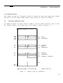
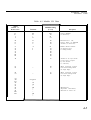
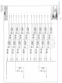
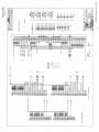
1
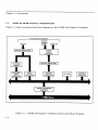
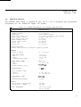
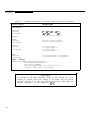
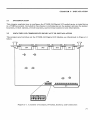
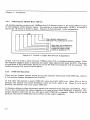
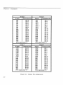
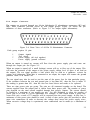
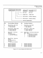
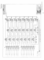
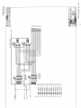
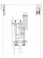
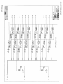
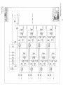
 XVME-244
6U 64-Channel Isolated Digital I/O Module
USER’S MANUAL
ACROMAG INCORPORATED
30765 South Wixom Road
P.O. BOX 437
Wixom, MI 48393-7037 U.S.A.
Tel: (248) 295-0885
Fax: (248) 624-9234
Email: [email protected]
Copyright 2012, Acromag, Inc., Printed in the USA.
Data and specifications are subject to change without notice.
8500-969A CHAPTER 1 -
1.1
INTRODUCTION
INTRODUCTION
The XVME-244 Digital I/O module provides VMEbus systems with 64 optically isolated I/O
channels, 32 input channels and 32 output channels. The inputs are arranged in four groups
of eight each. Each group is optically isolated from the others and from the VMEbus circuitry.
Typical applications for the XVME-244 Digital I/O module include:
l
l
l
0
l.2
Inputs
Outputs
Limit switches
Proximity switches
Photo detector switches
Control valves
Alarm interface
Parallel interface
Indicator lamps
Alarm trips
MANUAL STRUCTURE
The purpose of this first chapter is to introduce the user to the general specifications and
functional capabilities of the XVME-244 Digital I/O module. Chapter 2 will develop the
various aspects of module installation and operation. Chapter 3 provides the necessary
information needed to program the input and output data transfers. The appendices are
designed to introduce and reinforce a variety of module-related topics including: Xycom’s
Standard I/O Architecture, block diagram, and assembly drawings.
Chapter
One
-
A general description of the XVME-244 Digital I/O
module, including complete functional and environmental
specifications, VMEbus compliance information, and a
block diagram.
Chapter
Two
-
Module installation information covering the location of
pertinent module components, switch and jumper options,
external connector pin locations and standard board
installation information.
Chapter
Three
-
Provides information needed to program the input and
output data transfers
Appendix A
Xycom standard I/O architecture
Appendix B
Block diagram, assembly drawing, and schematics
XVME-244 Manual
December 1992
1.4
SPECIFICATIONS
The following Table (which is continued on page 1-4) is a list of operational and environmental
specifications for the XVME-244 Digital I/O module.
Table l-l. XVME-244 Digital I/O Module Specifications
CHARACTERISTIC
OUTPUTS
Number of channels
Configuration
Power supply voltage range
On-state output voltage
Power supply ground current
Off-state leakage current
On-state output current
Turn-on time
Turn-off time
SPECIFICATION
32 (4 groups of 8)
Current sourcing outputs
l0-15 VDC or 15-30 VDC, jumper selectable
(V supply - 0.8V) min.
35 mA max.
400 uA max.
400 mA max.
10 usec max.
120 usec max.
Transient Protection
Reverse voltage protection and transient suppression provided
INPUTS
Number of channels
32 (4 groups of 8)
Input Voltage Range
Logic 1
Logic 0
Typical threshold voltage
-35to +35
Input Current
0 to 14 mA
Range
Logic 1
Logic 0
Typical threshold current
10 to 35 VDC
-35 to 3 VDC
6 VDC
2.3 mA to 14 mA
oto400 /A
1.1 mA
Input Impedance
2.5 kQ min
Input Propagation Delay
Off-to-on
On-to-off
30 usec worst case
175 usec worst case
Input Debounce
1223ms
Time
Maximum Input Frequency
Isolation
Any I/O group to any I/O group
Any I/O group to VMEbus
Power
Requirements
2.8 KHz
300 VDC
1000 VDC
+5V @ 1.0 A typical
+5V @ 1.2 A max.
1-3
~~~-
Chapter I - Introduction
Table l-l. XVME-244 Digital I/O Module Specifications (Continued)
CHARACTERISTIC
SPECIFICATION
Environmental
Temperature
Operating
Non-operating
0’ to 65O C (32’ to 149’ F)’
-40’ to 85’ C (-40” to 185’ F)
Humidity
5 to 95% RH, non-condensing
Altitude
Operating
Non-operating
Sea level to 10,000 ft. (3048 m)
Sea level to 50,000 ft. (15240 m)
Vibration
Operating
Non-operating
Shock
Operating
Non-operating
.015” peak to peak
2.5 g peak acceleration
.030” peak to peak
5.0 g peak acceleration
30 g peak acceleration, 11 msec duration
50 g peak acceleration, 11 msec duration
VMEbus
Compliance
Complies with VMEbus specification, IEEE 1014, Rev. C.l
A24/A16:Dl6/D08(EO) DTB slave
Utility signals - SYSFAIL
Form factor: DOUBLE 233.35 mm x 160 mm (9.2” x 6.3)
Conforms to Xycom Standard I/O Architecture
*CAUTION
A fan rated at 40 CFM minimum should be used. Forced air is not
required in systems where the voltage on all inputs will not exceed
30 VDC. Forced air is also not required in systems which limit the
ambient temperature of the module to 4O’C.
1-4
XVME-244 Manual
December 1992
NOTE
The output registers cannot be set to a one state until SYSFAIL is
negated. When Jl is in the B position, the state of SYSFAIL has no
effect on the output registers
2.2.3
Output Power Supply Selection
Each output group has a jumper with which to select the power supply voltage range, (refer to
Figure 2-3 which shows the mapping of the output signals to the connector pins). When the
jumper is in the A position the voltage range is 15-30V. When the jumper is in the B position
the range is 10-l 5V. The power voltage should not go below the selected range as this could
cause damage to the output channel. Likewise, the power voltage should not exceed the selected
range as this could cause the group’s fuse to blow. Table 2-1 shows jumpers and their output
group.
Table 2-1. Jumper Output Groups
JUMPER
J4
J3
J5
J6
POSITION
A
A
A
A
15-30
15-30
15-30
15-30
B
B
B
B
l0-15
l0-15
l0-15
l0-15
GROUP
.
1
2
3
4
Vcc is monitored by a precision voltage comparator. Discrete circuitry will not allow the
outputs to turn on unless Vcc is within operational limits. When Vcc reaches its operational
limits, SYSRESET* will have reset the output registers to 0 and the outputs will not turn on.
The outputs are guaranteed to stay off during the application of external power. When
external power is being applied and either a 0 is written to the output register or the VMEbus
side is not powered on, the outputs will not turn on.
In cases where the VMEbus side is powered up and l’s are written to the output registers, the
external power supply should rise within a couple of seconds. This will prevent the output
transistors from lingering in the linear state and dissipating excessive power.
2-3
XVME-244 Manual
December 1992
2.2.4
Output
Connectors
The outputs are accessed through two 44-pin high-density D subminiature connectors (JK3 and
JK4). Each connector provides access to two output groups. Figure 2-4 shows the pin
definition of these connectors. (Refer to Figure 2-3 for output signal information).
Figure 2-4. Front View of 44 Pin D Subminiature Connector
Each group requires 19 pins:
8
1
9
1
Output signals
Test signal
Power supply (all tied together)
Power supply ground reference
When an output is turned on, current will flow from the power supply pins and come out
through the output pin. See Figure 2-5.
When an output is turned off, a small (leakage) current will try to flow out of the output. This
will raise the potential of the output to the power supply voltage level (if there is no load on
the output). The test signal provides a bias which may be used as a pulldown resistor for
system level debugging. When this is connected to an output, the output will assume the ground
potential when it is turned off.
The test signal may also be used to test the state of the power fuse for that particular group.
If the resistance between the test and ground pins is less than l0K, then the fuse is intact. If
the reading is greater than l0K, then the fuse has been blown and needs to be replaced.
There are nine power pins per group. The pins are all connected together on the board. The
current supplied from the output pins is drawn from these power pins. The number of power
pins depends on the total current supplied through that group’s outputs. The current should
be limited to a maximum of one ampere per pin. Use this limitation to select the number of
power pins to be used in a given application. For example, if each output within a group may
source 400 mA, a total of 3.2 amperes will be required from the power supply. In this case, a
minimum of four power pins should be used. A total of nine power pins are provided to allow
more wire connections in order to decrease the voltage drop across the power supply wires.
When excessive voltage drop is experienced, more connections can be made (to a maximum of
nine).
2-5
XVME-244 Manual
December 1992
2.2.6
Using the Inputs to Monitor the Outputs
Since the inputs are electrically compatible with the outputs, the inputs can be connected to the
outputs. This is beneficial in situations where the actual state of the output at the connector
must be monitored for reliability reasons.
The actual state of the outputs may differ from the output register image. The following lists
several reasons:
-
-
-
Power supply may fail, providing marginal power or no power
A short may exist in the system, such that the output cannot turn on or off
Output circuitry’s fuse may have blown
Hardware failure may have occurred on a particular output
By connecting the inputs to the outputs, the outputs’states at the connectors may be monitored
through the inputs and these fault conditions can be detected. Figure 2-9 shows the input and
output diagram.
NOTE
There is no minimum load requirement when the inputs are used to
monitor’the
outputs.
4
1PWR INPUTS
OUTPUT
GROUP
bUP
INPUT
GROUP
Figure
2-9.
Input
Monitoring
Output
Connection
Diagram
2-9
CHAPTER 3 - PROGRAMMING
* 3.1 INTRODUCTION
This chapter provides the information needed to program the input and output data transfers
and how to use the unique design features which are part of Xycom I/O modules.
3.2
.
MODULE MEMORY MAP
All address references are offsets which are added to the base address selected by SW1 to form
the VMEbus address. The memory map of the module is shown in Figure 3-1.
C3
0Cl
INPUT
REGISTERS
A2
A3
A0
Al
84
85
82
83
OUTPUT
REGISTERS
81
CONTROL REGISTER
FILTERED
INPUT
REGISTERS
3F
VMEbus DATA BIT
Figure 3-1.
Memory Map for XVME-244
3-1
Chapter 3 - Programming
3.3
MODULE REGISTERS
The following sections describe the XVME-244 registers residing in the VMEbus short I/O
memory space or the upper 64 Kbytes of the standard memory space.
3.3.1
Control Register (Base Address +8lH)
An eight bit read/write control register is provided to control module functions. Two bits
control the state of the PASS and FAIL LEDs on the front panel. One bit enables the outputs,
while the remaining bits may be used as read/write bits and do not affect module operation.
In response to SYSRESET, all output control register bits will go to 0. This will turn the FAIL
LED on, turn the PASS LED off, and enable the outputs.
The control register is located at offset 8 IH and has the following format:
I
Bit 0 (LSB)
Will assert SYSFAIL (if J2 is in A position) and turn
the FAIL LED on.
Will negate SYSFAIL and turn the FAIL LED off.
Bit 1
Will turn the PASS LED off.
Will turn the PASS LED on.
Bit 4
I
0
1
Will negate the clear condition of the output
registers.
Will clear all output registers which forces the
outputs off.
NOTE
If Bit 4 is 1 when writing to the output registers, the registers will
not accept the data.
3-2
XVME-244
Manual
December 1992
3.3.2
ID PROM (Base Address)
A 32 byte PROM is provided containing module identification information. This data is
available in odd bytes only. See Figure 3-2 for contents of ID PROM. Refer to Appendix A
for definitions of these bytes.
Offset
Address
01
03
05
07
09
OB
OD
OF
11
13
15
17
19
1B
1D
1F
21
23
25
27
29 - 3F
Contents
Hex
56
4D
45
49
44
58
59
43
32
34
34
20
20
20
20
31
20
31
31
20
00
Contents
ASCII
V
M
E
I
D
X
Y
C
2
4
4
1
1
1
Figure 3-2. ID PROM Contents
3.3.3
Output Registers (Base Address + 82h - 85h)
Four read/write output registers are provided, one for each output group. During reads, the
image of the outputs is provided, and a zero bit indicates that its corresponding output is off,
and a one bit indicates that it is on. All four registers are forced to zero upon the assertion of
SYSRESET, by setting bit 4 of the control register, or by the assertion of SYSFAIL (if Jl is in
the A positon). These registers may be accessed as bytes or 16 bit words. See Figure 3-1.
3.3.4
Input Registers (Base Address + Clh - C3h)
Four input registers are provided, one for each group. These registers are read only, providing
instantaneous state of the inputs. A zero bit indicates that the corresponding input is off, and
3-3
~~-
~
Chapter 3 - Programming
a one indicates that it is on. SYSRESET will have no effect on these registers. These registers
may be accessed as bytes or 16 bit words. See Figure 3-1.
3.3.5
Filtered Input Registers (Base Address + Alh - A3h)
The inputs are filtered by circuitry which will eliminate contact intermittency (bounce). This
will filter out the bouncing signals typical of mechanical switches. The input needs to switch
to a new state and stay in that state for 12 (* 3) mSec before the new state is passed to the
filtered input registers. If filtering is desired for a particular input, the filtered input register
should be used.
Four filtered input registers are provided, one for each input group. These registers are read
only, providing the state of the filtered inputs. A zero bit indicates that the corresponding
input is off, and a one indicates that it is on. SYSRESET will have no effect on these registers.
These registers may be accessed as bytes or 16 bit words. See Figure 3-1.
3-4
APPENDIX A -
A.1
XYCOM STANDARD I/O ARCHITECTURE
INTRODUCTION
The purpose of this appendix is to define Xycom’s Standard I/O Architecture for XVME I/O
modules. This Standard I/O Architecture has been incorporated on all Xycom XVME I/O
modules in offer to provide a simpler and more consistent method of programming for the
entire module line. The I/O Architecture specifies the logical aspects of bus interfaces, as
opposed to the “physical” or electrical aspects as defined in the VMEbus specifications. The
module elements which are standardized by the Xycom I/O Architecture are the following:
Module Addressing - Where a module is positioned in the I/O address space and
how software can read from it or write to it.
0
Module Identification - How software can identify which modules are installed
in a system.
Module Operational Status - How the operator can (through software) determine
the operational condition of specific modules within the system.
Interrupt Control - How software is able to control and monitor the capability
of the module to interrupt the system.
l
Communication Between Modules - How master (host) processors and intelligent
I/O modules communicate through shared global memory or the dual-access
RAM on the I/O modules.
I/O Kernel - How intelligent and non-intelligent “kernels” facilitate the
operation of all Xycom I/O modules.
A.2
MODULE ADDRESSING
All Xycom I/O modules are designed to be addressed within the VMEbus-defined 64K short
I/O address space. The restriction of I/O modules to the short I/O address space provides
separation of program/data address space and the I/O address space. This convention
simplifies software design and minimizes hardware and module cost, while at the same time,
providing 64K of address space for I/O modules.
A.2.1
Base Addressing
Since an I/O module connected to the bus must have its own unique base address, the base
addressing scheme for Xycom VME I/O modules has been designed to be jumper selectable.
Each XVME I/O module installed in the system requires at least a IK byte block of the short
I/O memory. This divides the 64K short I/O address space into 64 1K segments. Thus, each
I/O module has a base address which starts on a 1K boundary. As a result, the Xycom I/O
modules have all been implemented to decode base addresses in 1K (400H) increments. On an
intelligent XVME module, only address signals AI0-A13 are decoded, while A14 and Al 5 must
be zero. (This implies that only the lowest 16 of the possible 64 1K segments are used for
A-l
Appendix A - Xycom Standard I/O Architecture
intelligent I/O modules). On non-intelligent XVME modules, the six highest order short I/O
address bits are decoded, while the remaining lower order bits are ignored. This arrangement
provides the correct address configuration to allow each module address to begin on a IK
boundary.
Non-intelligent XVME modules allow the use of six base address jumpers
(representing bits Al0-A15), therefore, they are able to reside on any of the 64 1K boundaries
available in the short I/O address space. Intelligent XVME modules will only allow the use of
four base address jumpers (representing bits Al 0-Al 3) which limit their selection of 1K
boundaries to one of sixteen possible choices.
Figure A-l shows an abbreviated view of the short I/O memory.
BASE
SHORT I/O
ADDRESS SPACE
OOOOH
0400H
0800H
OCOOH
1OOOH
0
1
2
3
4
1400H
FCOOH
63
Figure A-l. 64K Short I/O Address Space
A-2
A.2.2 Standardized Module I/O Map
The IK block of short I/O addresses (called the I/O Interface Block) allocated to each XVME
module is mapped with a standardized format in order to simplify programming and data
access.
The locations of frequently used registers and module-specific identification
information are uniform. For example, the module identification information is always found
in the first 32 odd bytes of the module memory block; with these addresses being relative to the
jumpered base address (i.e., Module I.D. data address = base address + odd bytes 1H - 3FH). The
byte located at base address + 81H on each module contains a Status/Control register which
provides the results of diagnostics for verification of the module’s operational condition. The
remainder of the I/O Interface Block (base address + 82H - 3FFH) is module-specific and it
varies in size from one module to the next. It is in this area that the module holds specific
registers, buffers, I/O status, data and pointer registers, etc. All intelligent XVME I/O modules
have an area of their I/O Interface Blocks defined as “dual access RAM.” This area of memory
provides the space where XVME “slave” I/O modules access their command blocks and where
XVME “master” modules could access their command blocks (i.e., “master” modules can also
access global system memory).
Figure A-2, on the following page, shows an address map of an XVME I/O module interface
block, and how it relates to the VMEbus short I/O address space. Notice that any location in
the I/O Interface Block may be accessed by simply using the address formula:
Module Base Address + Relative Offset = Desired Location
A-3
XViWE-244 Manual
December 1992
Table A-l. Module I.D. Data
Offset
Relative to
Module Base
Contents
ASCII Encoding
(in hex)
1
3
5
7
9
V
M
E
1
D
56
4D
45
49
44
ID PROM identifier,
always “VMEID”
(5 characters)
B
D
F
X
Y
C
58
59
43
Manufacturer’s I.D.,
always “XYC” for XYCOM
modules (3 characters)
11
13
15
17
19
1B
1D
2
4
4
32
34
34
20
20
20
20
Module Model Number
(3 characters and
4 trailing blanks)
31
Number of 1K byte blocks
of I/O space occupied
by this module
(1 character)
1F
21
23
1
20
31
Major functional revision
level with leading blank
(if single digit)
25
27
1
31
20
Minor functional revision
level with trailing blank
(if single digit)
29
2B
2D
2F
31
33
35
37
39
3B
3D
Undefined
n
n
n
n
n
n
n
,
Descriptions
I
Manufacturer
Dependent Information,
Reserved for future use
Appendix A - Xycom Standard I/O Architecture
The module has been designed so that it is only necessary to use odd backplane addresses to
access the I.D. data. However, each of the 32 bytes of ASCII data have been assigned to the
first 32 odd I/O Interface Block bytes (i.e., odd bytes lH-3FH).
I.D. information can be accessed simply by addressing the module base, offset by the specific
address for the character(s) needed. For example, if the base address of the board is jumpered
to l000H, and if you wish to access the module model number (I/O interface block locations
11 H, 13H, 15H, 17H, 19H, lBH, and IDH), you will individually add the offset address to the
base address to read the hex-coded ASCII value at each location. In this example, the ASCII
values which make up the module model number are found sequentially at locations 101 IH,
10 13H, 1015H, 10 17H, 1019H, 10 lBH, and 1OlDH within the system’s short I/O address space.
A.4
MODULE
OPERATIONAL
STATUS/CONTROL
All XVME intelligent I/O modules are designed to perform diagnostic self-tests on power-up
or reset. For non-intelligent modules, the user must provide the diagnostic program. The selftest provision allows the user to verify the operational status of a module by either visually
inspecting the two LEDs which are mounted on the module front panel (see Figure A-3) or by
reading the module status byte, located at module base address + 81H.
Figure A-3 shows the location of the status LEDs on the module front panel. The two tables
included with Figure A-3 define the visible LED states for the module test conditions on both
the intelligent I/O modules and the non-intelligent I/O modules.
A-6
Appendix A - Xycom Standard I/O Architecture
The module status/control register (found at module base address + 8lH) on intelligent XVME
I/O modules provides the current status of the module self-test in conjunction with the current
status of the front panel LEDs. The status register on intelligent module is a “Read Only”
register and it can be read by software to determine if the board is operating properly.
On non-intelligent XVME I/O modules, the status/control register is used to indicate the state
of the front panel LEDs, and to set and verify module-generated interrupts. The LED status
bits are “Read/Write” locations which provide the user with the indicators to accommodate
diagnostic software. The Interrupt Enable bit is also a Read/Write location which must be
written to in order to enable module-generated interrupts. The Interrupt Pending bit is a “Read
Only” bit which indicates a module-generated pending interrupt.
Figure A-4, on the following page, shows the status/control register bit definitions for both
intelligent and non-intelligent XVME I/O modules.
A-8
Appendix A - Xycom Standard I/O Architecture
A.5
INTERRUPT CONTROL
Interrupts for non-intelligent modules can be enabled or disabled by setting/clearing the
Interrupt Enable bit in the module status register. The status of pending on-board interrupts
can also be read from this register. Interrupt control for intelligent modules is handled by the
Interprocessor Communications Protocol.
A.5.1
Communications
Between
Processors
Communications between an intelligent “master” and an intelligent “slave” I/O module is
governed by Xycom’s Interprocessor Communication (IPC) Protocol. This protocol involves the
use of 20-byte Command Block data structures, which can be located anywhere in shared global
RAM or dual-access RAM on an I/O module, to exchange commands and data between a host
processor and an I/O module. Interprocessor Communication Protocol is thoroughly explained
in Chapter 3 of this manual.
A.6
KERNEL
To standardize its XVME I/O modules, Xycom has designed them around “kernels” common
from module to module. Each different module type consists of a standard kernel, combined
with module-dependent application circuitry. Module standardization results in more efficient
module design and allows the implementation of the Standard I/O Architecture. The biggest
benefit of standardization for intelligent modules is that it allows the use of a common
command language or protocol (Interprocessor Communication Protocol in this case).
The intelligent kernel is based around a 68000 microprocessor. This design provides the full
compliment of VMEbus Requester and Interrupter options for master/slave interfacing, as well
as all of the advantages provided by the various facets of the Xycom Standard I/O
Architecture (as covered earlier in this appendix).
The non-intelligent kernel provides the circuitry required to receive and generate all of the
signals for a VMEbus defined 16-bit “slave” module. The non-intelligent kernel also employs
the features of the Xycom Standard I/O Architecture (as described earlier in this Appendix).
On the following page, simplified diagrams (Figure A-5) show the features of both the
intelligent and the non-intelligent kernels.
A-I0