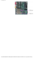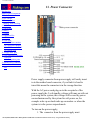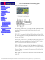
1
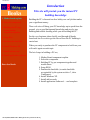
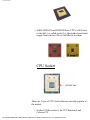
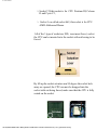
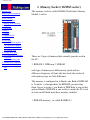
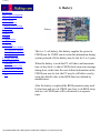
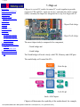
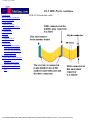
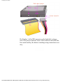
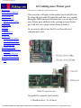
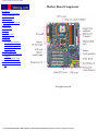
Mother Board Component Explain
Mother Board Component
Introduction
Mother Board Component
1.Clock Generator
2. CPU socket
3. Memory Socket
Memory error checking
4. ROM Bios
5. CMOS Ram
6. Battery
7. Chipset
8. Expansion Slot
9. AGP Port
10. IDE Ports
10.1 IDE Port continue
10.2 IDE Port continue
10.3 IDE Port with Raid
10.4 Serial ATA
11. Floppy Disk port
12. IO Connectors/USB ports
USB port
add more printer ports
13. Main Power Connector
14. Front Panel Connecting
Pin
All right reserved
file:///E|/WEB,/WEB12/2PC-Making/Mother%20Board/Mother%20Board%20Component.htm [16/3/46 20:39:33]
Introduction
Introduction
This site will provide you the instant PC
building knowledge
1. Mother board explain
2. Select the component
Building the PC is fun and can be a hobby or a real job that makes
you a significant money.
3. Building the PC step
by step putting
component togather
These web site will bring your PC knowledge up to speed from the
ground, give a good background knowledge and step by step
building and trouble shooting while you are building the PC.
4. Setup Bios
For the very beginner please briefly read through all books
from book one to seven to get the idea of how the PC building is
carried out.
5. Partition the hard disk
6. Install Windows XP
7. Install add on card
8. Install application software
Down load books
When you ready to purchase the PC component to build one your
self read it again on each topic.
The brief steps in building a PC are;
1. Mother Board component explain.
2. Select the component.
3. Building PC by put component together and
trouble shoot.
4. Setup BIOS
5. Partition the hard disk ( to make hard disk
recognizable by the system as drive C, drive
D and more).
6. Install Windows XP.
7. Install add on cards.
8. Install application Software's….and complete.
file:///E|/WEB,/WEB12/2PC-Making/index.htm [16/3/46 20:39:35]
1. Clock generator
1. Clock Generator
Introduction
Mother Board Component
1.Clock Generator
2. CPU socket
3. Memory Socket
Memory error checking
4. ROM Bios
5. CMOS Ram
6. Battery
7. Chipset
8. Expansion Slot
9. AGP Port
10. IDE Ports
10.1 IDE Port continue
10.2 IDE Port continue
10.3 IDE Port with Raid
10.4 Serial ATA
11. Floppy Disk port
12. IO Connectors/USB ports
USB port
add more printer ports
13. Main Power Connector
14. Front Panel Connecting
Pin
Simplify Clock distribution diagram
Clock generator on the mother board will generate the clock
signal called;
System bus clock or,
file:///E|/WEB,/WEB12/2PC-Making/Mother%20Board/1.Clock%20generator.htm (1 of 4) [16/3/46 20:39:37]
1. Clock generator
Front side bus clock.
Front side bus clock is a common reference signal that
distributed to almost all component on the mother board, it
also define the speed of the component.
The major component that use Front side bus clock are,
- The CPU
- The Memory
- AGP Port
- PCI bus
Changing the frequency of the front side bus clock will effect
all above component, higher clock frequency will make them
run faster, but the component has it's limitation of what speed
they can run.
The CPU
Front side bus clock distributed to the CPU, in side the CPU
front side bus clock will be multiplied by the multiplying
circuit to make the frequency high enough to reach the core
clock frequency of the CPU.
For example if the front side bus is 100 Mhz and the core
clock of the CPU is 1.1 Ghz the front side bus must be
multiplied by 11 ( 100 x 11 = 1100 Mhz or 1.1 Ghz ).
There are many types of front side bus clock for to day's
mother board.
1.
Front side bus 400/533 Mhz this mean that the mother
board will generate either 400 or 533 Mhz, the user can
chose to have the mother board to generate clock 400 or
533
533MHz front side bus is for Pentium 4 at 3.06 GHz,
2.80 GHz, 2.66 GHz, 2.53 GHz, 2.40B GHz, 2.26 GHz
file:///E|/WEB,/WEB12/2PC-Making/Mother%20Board/1.Clock%20generator.htm (2 of 4) [16/3/46 20:39:37]
1. Clock generator
400MHz system bus is for Pentium 4 at 2.60 GHz, 2.50
GHz, 2.40 GHz, 2.20 GHz, 2A GHz, 2 GHz, 1.90 GHz,
1.80 GHz, 1.70 GHz
2.
Front side bus 200/266/333 the mother board with this
front side bus is for CPU AMD Athlon or Duron
or Pentium 4.
3.
Front side bus 100/133 the mother board with this front
side bus is for CPU Pentium III or Celeron II and
Pentium 4.
for example;
CPU Celeron 1.4 Ghz use Front side bus clock 100
multiply by 14.
The front side bus clock, one of the two ( 400 or 533, 200 or
266, 100 or 133 ) on the mother board is selectable by the user
by using,
1. The switch on the mother board or,
2. The Jumper on the mother board or,
3. By CMOS setup.
The front side is very much directly related to the frequency
used by the memory ( not a must ) for example ,
RDRAM use front side bus 400 Mhz
DDR ram use front side bus 200, 266, 333, 400
SD Ram use front side bus 100 or 133 Mhz
Over clocking the CPU
Is a way to make the CPU run at a higher clock frequency that
specified by the manufacturer, in the old day of CPU socket 7
the clock multiplier switch or jumper is mounted on the
mother board and they are easily to be changed, changing the
switch setting will change the multiplier, we can over clock
file:///E|/WEB,/WEB12/2PC-Making/Mother%20Board/1.Clock%20generator.htm (3 of 4) [16/3/46 20:39:37]
1. Clock generator
the CPU by two ways,
1. Choose the bigger multiplier figure to multiply,
for example with CPU 400 Mhz is 100 Mhz front
side bus
multiply by 4, over clock this CPU to make this
CPU run at 500 Mhz we multiply by using 5.
2. Choose the higher Front side bus frequency,
with the mother board that has front side bus 100
and 133 Mhz, can choose 100 or 133 to supply to
the CPU, with CPU 400, we choose 133 x 4 the
CPU will run at 532 Mhz.
Some mother board has more than 2 step of front side bus
clock for the user to choose this makes more flexible to do
ocverclocking.
With to day's CPU, you may not be able to change the
multiplier but you may still can change the front side bus, and
remember changing the front side bus will effect all of
the component on the mother board, Memory, AGP port and
PCI Bus and etc.
Note The web site of the CPU manufacturer should have
the information of which CPU will use what frequency of the
Front side bus.
file:///E|/WEB,/WEB12/2PC-Making/Mother%20Board/1.Clock%20generator.htm (4 of 4) [16/3/46 20:39:37]
2. CPU Socket
2. CPU Socket
Introduction
Mother Board Component
1.Clock Generator
2. CPU socket
3. Memory Socket
Memory error checking
4. ROM Bios
5. CMOS Ram
6. Battery
7. Chipset
8. Expansion Slot
9. AGP Port
10. IDE Ports
10.1 IDE Port continue
10.2 IDE Port continue
10.3 IDE Port with Raid
10.4 Serial ATA
11. Floppy Disk port
12. IO Connectors/USB ports
USB port
add more printer ports
13. Main Power Connector
14. Front Panel Connecting
Pin
There are 4 types of the CPU that are currently popular in the
market.
1.
Intel PENTIUM 4 and Celeron 478 these CPU's will fit
in to socket 478, the mother board must supply front
side bus 400 or 533 Mhz. to use them.
2.
Pentium III and CELERON II these CPU's will fit in to
socket 370, the mother board must supply front side bus
100 or 133 Mhz. to use them.
3.
VIA Cyrix C3, this CPU will fit in to socket 370, the
mother board must supply front side bus 100 or 133
Mhz to use them.
file:///E|/WEB,/WEB12/2PC-Making/Mother%20Board/2.%20CPU%20Socket.htm (1 of 4) [16/3/46 20:39:40]
2. CPU Socket
4.
AMD ATHLON and DURON these CPU's will fit in to
socket 468 ( or called socket A ), the mother board must
supply front side bus 200 or 266 Mhz to use them.
CPU Socket
There are 3 type of CPU Socket that are currently popular in
the market,
1.
Socket 478 this socket is for CPU Pentium 4 and
Celeron 478.
file:///E|/WEB,/WEB12/2PC-Making/Mother%20Board/2.%20CPU%20Socket.htm (2 of 4) [16/3/46 20:39:40]
2. CPU Socket
2.
Socket 370 this socket is for CPU Pentium III, Celeron
II and Cyrix C3,
3.
Socket A or called socket 462, this socket is for CPU
AMD Athlon and Duron.
All of the 3 type of socket are ZIF ( zero insert force ) socket
the CPU can be inserted in to the socket with out having to be
forced.
By lift up the socket actuator arm 90 degree the socket hole
array are opened, the CPU can now be dropped into the
socket with out being forced, make sure that the CPU is fully
seated on the socket.
file:///E|/WEB,/WEB12/2PC-Making/Mother%20Board/2.%20CPU%20Socket.htm (3 of 4) [16/3/46 20:39:40]
2. CPU Socket
Before insert the CPU in to the socket make sure that pin one
of the CPU is aligned with pin one of the socket as indicated
above.
file:///E|/WEB,/WEB12/2PC-Making/Mother%20Board/2.%20CPU%20Socket.htm (4 of 4) [16/3/46 20:39:40]
3.Memory socket
3. Memory Socket ( DIMM socket )
Introduction
Mother Board Component
1.Clock Generator
2. CPU socket
3. Memory Socket
Memory error checking
4. ROM Bios
5. CMOS Ram
6. Battery
7. Chipset
8. Expansion Slot
9. AGP Port
10. IDE Ports
10.1 IDE Port continue
10.2 IDE Port continue
10.3 IDE Port with Raid
10.4 Serial ATA
11. Floppy Disk port
12. IO Connectors/USB ports
USB port
add more printer ports
13. Main Power Connector
14. Front Panel Connecting
Pin
The memory socket is called DIMM ( Dual Inline Memory
Module ) socket.
There are 3 types of memory that currently popular used in
the PC,
1. RDRAM 2. DDR ram 3. SDRAM
each type of memory are difference in speed and use
difference frequency of front side bus clock, the socket of
each memory type are little difference.
The memory is configured in to Banks, one Bank of RDRAM
is 2 sockets ( when purchase the RDRAM you must buy
them 2 piece at a time ), one Bank of DDR Ram is one socket
and one Bank of SDRAM is one socket, to make the PC work
at least one full bank must have memory installed.
1. RDRAM memory ( or called RAMBUS )
file:///E|/WEB,/WEB12/2PC-Making/Mother%20Board/3.%20Memory%20Socket.htm (1 of 4) [16/3/46 20:39:43]
3.Memory socket
This type of memory is used mainly in Pentium 4 mother
board, it use front side bus clock at 400 Mhz, it has highest
performance and is most expensive.
RDRAM Socket
The memory will have 2 notches and the socket will have 2
keys to prevent different type of memory to fit in.
One bank of the memory is two sockets and must have 2
memory stick installed, if there are some bank that do not
have memory installed the empty bank must have C-RIMM
installed.
C-RIMM
C-RIMM is a dummy stick that has no memory chip on it, it
is used to to complete the memory circuit, when you buy the
mother board with RDRAM sockets please make sure that CRIMM's come with the mother board .
Please refer to the mother board user manual for which slot to
install RDRAM and which slot to install C-RIMM.
2. DDR ram
file:///E|/WEB,/WEB12/2PC-Making/Mother%20Board/3.%20Memory%20Socket.htm (2 of 4) [16/3/46 20:39:43]
3.Memory socket
DDR Ram is a medium high performance memory and
medium price, it is a very popular memory to day, it is used
in Pentium 4, and AMD Athlon and Duron mother board, use
front side bus at 200, 266, 333 and
400 Mhz.
DIMM socket for DDR Ram
One memory bank is one socket, and can be 128 MB, 256
MB, 512 MB.
3. SDRAM
This is a lowest performance memory of the 3 types and
lowest price, this type of memory use front side bus 100 or
133 Mhz, it is used mainly in socket 370 mother board
( Pentuim III, Celeron II, Cyrix C3 ) and also in Pentium 4
mother board with front side bus clock at 100 or 133 Mhz.
SDRAM
SDRAM socket
file:///E|/WEB,/WEB12/2PC-Making/Mother%20Board/3.%20Memory%20Socket.htm (3 of 4) [16/3/46 20:39:43]
3.Memory socket
One bank of SDRAM is one socket and it can be 128 Mb, 256
MB and so on.
file:///E|/WEB,/WEB12/2PC-Making/Mother%20Board/3.%20Memory%20Socket.htm (4 of 4) [16/3/46 20:39:43]
3.1 Memory error checking
3.1 Memory Error checking
Introduction
Mother Board Component
1.Clock Generator
2. CPU socket
3. Memory Socket
Memory error checking
4. ROM Bios
5. CMOS Ram
6. Battery
7. Chipset
8. Expansion Slot
9. AGP Port
10. IDE Ports
10.1 IDE Port continue
10.2 IDE Port continue
10.3 IDE Port with Raid
10.4 Serial ATA
11. Floppy Disk port
12. IO Connectors/USB ports
USB port
add more printer ports
13. Main Power Connector
14. Front Panel Connecting
Pin
Memory error checking
Data in a byte written in to the Memory and later on read
back if the Memory has some problem the data read back
may pick up some extra bit or drop some bit.
Parity Bit
One way of checking error is by using the Parity bit, before
the byte of 8 bit is wrote to the memory, the memory
controller will count the number of bit in a byte and if the
number of bit is Even the circuit will add one more bit in to
that byte to make them Odd this bit being added is called
Parity bit, the byte become 9 bit byte, when the byte is read
from the memory the controller expect to see the number of
bit in Odd, if a bit was pick up or dropped the number of bit
become even and the memory controller will recognized that
this is an error and if 2 bits were picked up or drop the parity
checking will not able to detect error.
ECC ( error checking and correction )
The more accurate in checking memory error is by implement
ECC the ECC process is done by calculate the Syndrome byte
from a multiple data byte normally use 8 byte ( 64 bit )
the Syndrome byte is wrote together with the data byte and
when the data is read back the Syndrome will be calculated
again and compare with the Syndrome byte read if they are
the same then the data read is no error.
The ECC process can can correct single bit error automatic
with out the system being notified and if there are multiple bit
error ECC can recognize and notify the system.
The Mother board must support Parity or ECC Memory to to
be able to use them.
file:///E|/WEB,/WEB12/2PC-Making/Mother%20Board/3.1%20Memory%20error%20checking.htm (1 of 2) [16/3/46 20:39:44]
3.1 Memory error checking
file:///E|/WEB,/WEB12/2PC-Making/Mother%20Board/3.1%20Memory%20error%20checking.htm (2 of 2) [16/3/46 20:39:44]
4. ROM BIOS
4. ROM BIOS
Introduction
Mother Board Component
1.Clock Generator
2. CPU socket
3. Memory Socket
Memory error checking
4. ROM Bios
5. CMOS Ram
6. Battery
7. Chipset
8. Expansion Slot
9. AGP Port
10. IDE Ports
10.1 IDE Port continue
10.2 IDE Port continue
10.3 IDE Port with Raid
10.4 Serial ATA
11. Floppy Disk port
12. IO Connectors/USB ports
USB port
add more printer ports
13. Main Power Connector
14. Front Panel Connecting
Pin
BIOS ( Basic Input Output System ) BIOS is a program that
work as a part of the hardware, the program is stored in the
read only memory ( ROM ) ROM can retain BIOS
permanently even though electric power was removed from
the system.
BIOS will start work immediately when the PC is powered
on, BIOS will make the hardware ready and the IO ( in put
out put devices ) works at the initial state, Floppy disk and
CD-ROM able to read and boot, PC able to detect the
installed hard disk, the screen able to display, all this will help
us to be able to install the Operating System or install
Windows.
The brief function of the BIOS that we want to discuss here
are;
1.
Bios test the hardware component on the mother board,
❍
❍
❍
Test the CPU
Test The memory
Initialize and test the hardware and Chipset on the
mother board.
This is called POST( Power On Self Test ) If BIOS
found any hardware error during test it will generate
POST code and Beep code.
file:///E|/WEB,/WEB12/2PC-Making/Mother%20Board/4.ROM%20Bios.htm (1 of 3) [16/3/46 20:39:46]
4. ROM BIOS
The POST code is a 2 digit hexadecimal code, will
display on the POST display card during powering on,
we will have to plug the POST Display card on the
expansion slot before we power on the PC, this card is
very helpful in doing trouble shooting the dead PC.
The POST display card is available to be purchased on
the internet, you can search by using key word Power
On Self Test.
The meaning of the post code is varied depends on the
manufacturer of the BIOS, with Award BIOS code C6
mean the memory is not working properly, code 42
mean hard disk is not found.
The Beep code is a sound generated by BIOS during
POST, this is another aid to help diagnose the PC
hardware problem, with Award BIOS, if the memory
error is found the series of long beep sound will be
generated, beep.......beep......beep.
2.
3.
Bios has utilities to detect the installed hard disk.
Bios controls input out put component,
Communication ports
Printer port
Hard disk
Floppy disk
Bios manage power saving of the PC.
Bios has utility to enter CMOS setup ( or called Bios
setup ).
After all hardware tested successfully Bios will read (
Boot ) the operating system from the boot device, the
boot devices is definable by the user, the default boot
devices is the sequence of A:, then C: with this
sequence the PC will boot from drive A: the floppy disk
first and if drive A does not have the floppy to read the
PC will skip drive A: and boot from drive C:, the hard
disk, if we want to install Windows from bootable CD❍
❍
❍
❍
4.
5.
6.
file:///E|/WEB,/WEB12/2PC-Making/Mother%20Board/4.ROM%20Bios.htm (2 of 3) [16/3/46 20:39:46]
4. ROM BIOS
Rom we have to specify the boot sequence start from
CD-Rom.
To specify the boot device, you must enter the CMOS
setup utilities, most of the cloned PC we can go to the
CMOS setup by pressing the delete key during boot, at
the CMOS setup screen menu go to BIOS features
setup, then move the cursor to the boot sequence and
select the device you want to boot from by pressing the
page up or page down on the key board to select the
boot device.
BIOS Update
Bios is a program, after some time it is released to the
user, it may need to updated to support some newly
manufactured hardware or some problem was
discovered or new version is released.
BIOS update is done by a special program that has the
ability to write the new version of BIOS in to ROM.
Prior to do the BIOS update we recommend that old
BIOS in the ROM should be read and save, in case if the
new BIOS does not give the satisfactory result due to
the data error or the file was damaged we can still write
the old BIOS back.
The BIOS update program and the new version of BIOS
can be downloaded from the Mother board
manufacturer, the program may be run stand alone by
boot it from the diskette or run under Windows, after the
ROM is written with the new version of BIOS the PC
must be reboot to make new BIOS take control of the
system.
file:///E|/WEB,/WEB12/2PC-Making/Mother%20Board/4.ROM%20Bios.htm (3 of 3) [16/3/46 20:39:46]
5. CMOS RAM
5. CMOS Ram
Introduction
Mother Board Component
1.Clock Generator
2. CPU socket
3. Memory Socket
Memory error checking
4. ROM Bios
5. CMOS Ram
6. Battery
7. Chipset
8. Expansion Slot
9. AGP Port
10. IDE Ports
10.1 IDE Port continue
10.2 IDE Port continue
10.3 IDE Port with Raid
10.4 Serial ATA
11. Floppy Disk port
12. IO Connectors/USB ports
USB port
add more printer ports
13. Main Power Connector
14. Front Panel Connecting
Pin
Because the ROM BIOS is a read only memory and we are
not able to store the user defined information which is needed
by bios to run, the information such as,
●
●
●
●
●
●
The boot sequence A, C, CD-ROM
The hard disk and floppy disk size
The information of how the user wants the
BIOS to work.
The parameter for chipset to work.
IO port address and how they should work.
Time of day clock and the password .... and
more.
Every time the PC is powered on BIOS will use the above
information, these information may be changed by the user
and must retained in the memory even though the electric
power is removed from the system, the memory that is used
to store these information is called CMOS Ram, CMOS
Ram is located on the mother board and will need the power
from battery during PC powered off to retain the
information.
The password that was set during CMOS setup time will al so
stored in the CMOS Ram, if the password was forgot or
password need to be cleared this can be done by remove the
battery and leave the mother board with out battery for a big
while, the other proper way and faster to clear CMOS is by
using clear CMOS jumper on the mother board, please
consult mother board user manual for location on the mother
board and how to use, please remember after using jumper to
clear CMOS the jumper must be set back to normal, if not
then the PC will not boot.
After CMOS was cleared the stored information will
disappeared, CMOS setup must be performed and the time of
day clock will has to be set again.
file:///E|/WEB,/WEB12/2PC-Making/Mother%20Board/5.CMOS%20Ram.htm [16/3/46 20:39:47]
6. Battery
6. Battery
Introduction
Mother Board Component
1.Clock Generator
2. CPU socket
3. Memory Socket
Memory error checking
4. ROM Bios
5. CMOS Ram
6. Battery
7. Chipset
8. Expansion Slot
9. AGP Port
10. IDE Ports
10.1 IDE Port continue
10.2 IDE Port continue
10.3 IDE Port with Raid
10.4 Serial ATA
11. Floppy Disk port
12. IO Connectors/USB ports
USB port
add more printer ports
13. Main Power Connector
14. Front Panel Connecting
Pin
This is a 3 volt battery, this battery supplies the power to
CMOS ram for CMOS ram to retain the information during
system powered off, the battery may be last for 5 or 6 years.
When the battery is weak the PC will show and inaccurate
time of day clock, or show CMOS check sum error message
during boot, at this time the user defined information in the
CMOS ram may be lost, the PC may be still able to run by
using the default value in the BIOS that was defined by
manufacturer.
After the battery is replaced the BIOS parameter may need
be fine tune and save in CMOS ram, how to do BIOS setup
and save in CMOS ram will be discussed in a separate
topic.
file:///E|/WEB,/WEB12/2PC-Making/Mother%20Board/6.%20Battery.htm [16/3/46 20:39:49]
7. Chipset
7. Chip set
Introduction
Mother Board Component
1.Clock Generator
2. CPU socket
3. Memory Socket
Memory error checking
4. ROM Bios
5. CMOS Ram
6. Battery
7. Chipset
8. Expansion Slot
9. AGP Port
10. IDE Ports
10.1 IDE Port continue
10.2 IDE Port continue
10.3 IDE Port with Raid
10.4 Serial ATA
11. Floppy Disk port
12. IO Connectors/USB ports
USB port
add more printer ports
13. Main Power Connector
14. Front Panel Connecting
Pin
Chip set is a set of IC, used to be many IC’s work together to provide
support to CPU and I/O ( input out device ) and make the whole system
works, currently the chipset are integrated in to very few large scale IC.
The most chipset today's composed of to component,
- North bridge and
- South bridge
The North bridge will work closely with CPU, Memory and AGP port.
The south bridge will control the IO's
Intel(R) 850 Chipset
Chipset will determine the capability of the mother board, for example,
file:///E|/WEB,/WEB12/2PC-Making/Mother%20Board/7.%20Chipset.htm (1 of 2) [16/3/46 20:39:51]
7. Chipset
- what is the type and maximum speed of the CPU can be used with this
mother board.
- what is the type, speed and how many megabyte of memory ( SDRAM,
DDR RAM, RDRAM ), can be installed on this mother board, chipset
will control the memory operation.
- what type of Hard Disk this mother board will support
( DMA 66, ATA, 100, ATA 133 or serial ATA ).
- speed of AGP port ( 1X/2X, 4X/8X )
- the number of PCI slot.
- the number and speed of USB port on this mother board.
- Chipset also includes the control function of the PC system, IRQ
controller, DMA controller.
Some example of the chipset at the time this book is being written are;
Intel 850E for Pentium 4 and Celeron 478 with RDRAM.
Intel 845PE for Pentium 4 and Celeron 478 with DDR RAM speed 333
or 266 Mhz,
Intel 845GV for Pentium 4 and Celeron 478 with DDR RAM speed 266
or 200 Mhz. or SDRAM speed 100 or 133 Mhz.
AMD 760 MPX for AMD Athlon MP processor with DDR RAM 266
Mhz speed.
AMD 760 MP for AMD Athlon MP processor with DDR RAM speed
266 Mhz.
AMD 760 for AMD Athlon and Duron Processor with DDR RAM speed
200/266 Mhz.
file:///E|/WEB,/WEB12/2PC-Making/Mother%20Board/7.%20Chipset.htm (2 of 2) [16/3/46 20:39:51]
8. Expansion slot
8. Expansion Slot ( PCI type )
Introduction
Mother Board Component
1.Clock Generator
2. CPU socket
3. Memory Socket
Memory error checking
4. ROM Bios
5. CMOS Ram
6. Battery
7. Chipset
8. Expansion Slot
9. AGP Port
10. IDE Ports
10.1 IDE Port continue
10.2 IDE Port continue
10.3 IDE Port with Raid
10.4 Serial ATA
11. Floppy Disk port
12. IO Connectors/USB ports
USB port
add more printer ports
13. Main Power Connector
14. Front Panel Connecting
Pin
Expansion slot or Expansion bus is the slot that enable the
user to add the adapter card for additional function to the
system for example,
- Sound card or Multimedia card.
- LAN card.
- SCSI controller card.
- Internal Modem card.
- TV tuner card.
- Additional hard disk controller card.
or other special purpose adapter card.
The expansion slot that currently very popular and use by
every mother boards is the PCI Bus ( Peripheral Component
Inter connect ).
These card after inserted in to the slot may need the driver
software to be installed with the operating system to make the
card works.
PCI slot is the 32 bit bus running at clock speed 33 Mhz, the
maximum transfer speed of PCI bus is 133 megabyte/second.
The other type of Expansion slot is ISA slot, this is 16 bit bus
running at clock speed 8.33 Mhz data transfer rate is 16
Mbyte/sec, it has been widely used in the pass, today's mother
board it is very rare.
file:///E|/WEB,/WEB12/2PC-Making/Mother%20Board/8.%20Expansion%20Bus.htm (1 of 2) [16/3/46 20:39:53]
8. Expansion slot
file:///E|/WEB,/WEB12/2PC-Making/Mother%20Board/8.%20Expansion%20Bus.htm (2 of 2) [16/3/46 20:39:53]
9. AGP port
9. AGP Port
Introduction
Mother Board Component
1.Clock Generator
2. CPU socket
3. Memory Socket
Memory error checking
4. ROM Bios
5. CMOS Ram
6. Battery
7. Chipset
8. Expansion Slot
9. AGP Port
10. IDE Ports
10.1 IDE Port continue
10.2 IDE Port continue
10.3 IDE Port with Raid
10.4 Serial ATA
11. Floppy Disk port
12. IO Connectors/USB ports
USB port
add more printer ports
13. Main Power Connector
14. Front Panel Connecting
Pin
AGP ( Accelerated Graphic Port ) port is a high speed data
transfer port, this port is used by the display adapter card that
demands so much data with in short period of time.
The way AGP port works is similar to the PCI bus, AGP port
runs at clock speed 66 Mhz, with in one clock cycle of AGP
operation, the multiple of 32 byte can be transferred.
The speed of AGP port can be 1x, 2x, and 4x, 8x of PCI
speed.
AGP adapter card 1x/2x is using 3.3 volt power,
AGP adapter card 4x/8x is using 1.5 volt power.
Some mother board has got the universal AGP port connector
that can accept 1x/2x or 4x/8x card, the mother board with
this type of port should have the jumper for the user to set for
selection of using 1x/2x or 4x/8x AGP card .
Or some mother board only support one type of AGP card.
The mother board may not boot if the wrong type of card is
plugged.
file:///E|/WEB,/WEB12/2PC-Making/Mother%20Board/9.%20AGP%20Port.htm (1 of 2) [16/3/46 20:39:55]
9. AGP port
file:///E|/WEB,/WEB12/2PC-Making/Mother%20Board/9.%20AGP%20Port.htm (2 of 2) [16/3/46 20:39:55]
10. IDE port
10. IDE Ports
Introduction
Mother Board Component
1.Clock Generator
2. CPU socket
3. Memory Socket
Memory error checking
4. ROM Bios
5. CMOS Ram
6. Battery
7. Chipset
8. Expansion Slot
9. AGP Port
10. IDE Ports
10.1 IDE Port continue
10.2 IDE Port continue
10.3 IDE Port with Raid
10.4 Serial ATA
11. Floppy Disk port
12. IO Connectors/USB ports
USB port
add more printer ports
13. Main Power Connector
14. Front Panel Connecting
Pin
IDE ports, the 40 pin connector, these ports are for
connecting hard disk drives or IDE CD-ROM or IDE CD
writer.
There two type of hard disk that can be connected to this
ports;
●
●
ATA interface hard disk ( Advance Technology
Attached )
Pre ATA, they were called DMA 33 and PIO hard disk (
Programmable Input Output )
ATA Interface
The current hard disk interface are
- UDMA 66 data transfer rate 66 Mbyte/sec.
- ATA 100 data transfer rate 100 Mbyte/sec.
- ATA 133 data transfer rate 133 Mbyte/sec.
file:///E|/WEB,/WEB12/2PC-Making/Mother%20Board/10.%20IDE%20Port.htm (1 of 3) [16/3/46 20:39:57]
10. IDE port
Most of today’s hard disk drive are ATA100 or
ATA133 enabled.
The IDE cable for ATA hard disk is a flat cable with 80 wires
connect to 40 pin connecter on the mother board, 40 extra
wires are for noise shield.
The hard disk must compiled with UDMA 66, ATA 100 or
133 to be able transfer at the mother board's ATA specify
speed.
DMA 33
The data tranfer rate of DMA 33 is 33 Mbyte/sec
PIO Hard disk
The hard disk prior to ATA time were operated in PIO mode
there are 5 modes of PIO, PIO mode 5 is the highest data
transfer rate and is 22 Mbyte/sec.
The flat IDE cable for DMA 33 and PIO is 40 wire cable.
One of these two ports is called Primary IDE and the other
port called Secondary IDE.
Primary IDE can have 2 hard disk drives connected on the
IDE cable,
- one hard disk is called Master ( Primary Master ).
- the other hard disk is called Slave ( Primary Slave ).
Secondary IDE also can have 2 hard disk drives connected on
the IDE cable,
- one hard disk is called Master ( Secondary Master ).
- the other hard disk is called Slave ( Secondary Slave ).
CD-ROM can be connected on the same cable with hard disk
and should always be connected to Secondary IDE and
configure as a slave device.
To identify which port is Primary IDE and which port is
file:///E|/WEB,/WEB12/2PC-Making/Mother%20Board/10.%20IDE%20Port.htm (2 of 3) [16/3/46 20:39:57]
10. IDE port
Secondary IDE please consult the Mother Board user manual.
The standard configuration of the mother board will have 2
IDE ports and can connect up to maximum of 4 drives.
next
file:///E|/WEB,/WEB12/2PC-Making/Mother%20Board/10.%20IDE%20Port.htm (3 of 3) [16/3/46 20:39:57]
10.1 IDE port continue
10.1 IDE Ports continue
Introduction
Mother Board Component
1.Clock Generator
2. CPU socket
3. Memory Socket
Memory error checking
4. ROM Bios
5. CMOS Ram
6. Battery
7. Chipset
8. Expansion Slot
9. AGP Port
10. IDE Ports
10.1 IDE Port continue
10.2 IDE Port continue
10.3 IDE Port with Raid
10.4 Serial ATA
11. Floppy Disk port
12. IO Connectors/USB ports
USB port
add more printer ports
13. Main Power Connector
14. Front Panel Connecting
Pin
There are jumpers on the hard disk drive these jumpers will
configure the hard disk to a master or a slave, with UDMA
66, ATA 100 or ATA 133 the jumper should always set at
cable select.
With jumper set at cable select the hard disk that is connected
at the end of the cable will be a Master drive and the drive
that is connected at the middle of the cable is a Slave drive,
same on both primary and secondary IDE cable.
With the non ATA disk drive ( PIO and DMA 33 disk drive ),
to make them Master or Slave the jumpers are set differently.
The way of setting jumper of different hard disk manufacturer
can be difference.
For Seagate disk drive please see the picture below, or you
can go to the web site of each hard disk manufacturer for the
detail of jumper setting.
file:///E|/WEB,/WEB12/2PC-Making/Mother%20Board/10.1%20IDE%20Port%20continue.htm (1 of 2) [16/3/46 20:39:59]
10.1 IDE port continue
previous
next
file:///E|/WEB,/WEB12/2PC-Making/Mother%20Board/10.1%20IDE%20Port%20continue.htm (2 of 2) [16/3/46 20:39:59]
10.2 IDE port continue
10.2 IDE Ports continue
Introduction
Mother Board Component
1.Clock Generator
2. CPU socket
3. Memory Socket
Memory error checking
4. ROM Bios
5. CMOS Ram
6. Battery
7. Chipset
8. Expansion Slot
9. AGP Port
10. IDE Ports
10.1 IDE Port continue
10.2 IDE Port continue
10.3 IDE Port with Raid
10.4 Serial ATA
11. Floppy Disk port
12. IO Connectors/USB ports
USB port
add more printer ports
13. Main Power Connector
14. Front Panel Connecting
Pin
IDE ATA Hard disk cable
file:///E|/WEB,/WEB12/2PC-Making/Mother%20Board/10.2%20IDE%20Port%20continue.htm (1 of 2) [16/3/46 20:40:02]
10.2 IDE port continue
Pin Number 1 of the IDE connector on the hard disk is always
near to the power connector, most of the connector and cable also
have notch and key the chance in making wrong connection is not
easy.
file:///E|/WEB,/WEB12/2PC-Making/Mother%20Board/10.2%20IDE%20Port%20continue.htm (2 of 2) [16/3/46 20:40:02]
10.3 IDE port continue
10.3 IDE Ports with RAID capability
Introduction
Mother Board Component
1.Clock Generator
2. CPU socket
3. Memory Socket
Memory error checking
4. ROM Bios
5. CMOS Ram
6. Battery
7. Chipset
8. Expansion Slot
9. AGP Port
10. IDE Ports
10.1 IDE Port continue
10.2 IDE Port continue
10.3 IDE Port with Raid
10.4 Serial ATA
11. Floppy Disk port
12. IO Connectors/USB ports
USB port
add more printer ports
13. Main Power Connector
14. Front Panel Connecting
Pin
Some mother board may want to include the extra IDE port
together with special function of the port.
The mother board shown here for example, give 2 more IDE port
by using separate IDE controller, this 2 ports can have 2 hard disk
drives connected to each of them, in total of 2 ports can have 4
hard disks connect to them using 80 wires 40 pins ATA cable and
these 4 Hard disk drive can be configured as RAID device (
Redundancy Array of Independent Disk ).
Configured more than one hard disk drive in to RAID system will
make them capable of data protection, this mean that the same data
will stored in to more than one hard disk during write and if one
hard disk fail the data still available in the other hard disk, the
file:///E|/WEB,/WEB12/2PC-Making/Mother%20Board/10.3%20IDE%20Port%20continue.htm (1 of 2) [16/3/46 20:40:04]
10.3 IDE port continue
system still continue to run with out losing data, please consult the
mother user manual for how to use them.
file:///E|/WEB,/WEB12/2PC-Making/Mother%20Board/10.3%20IDE%20Port%20continue.htm (2 of 2) [16/3/46 20:40:04]
10.4 Serial ATA port
10.4 Serial ATA
Introduction
Mother Board Component
1.Clock Generator
2. CPU socket
3. Memory Socket
Memory error checking
4. ROM Bios
5. CMOS Ram
6. Battery
7. Chipset
8. Expansion Slot
9. AGP Port
10. IDE Ports
10.1 IDE Port continue
10.2 IDE Port continue
10.3 IDE Port with Raid
10.4 Serial ATA
11. Floppy Disk port
12. IO Connectors/USB ports
USB port
add more printer ports
13. Main Power Connector
14. Front Panel Connecting
Pin
Serial ATA is a new design of the hard disk interface.
On some of the new released mother board you may find the
port called Serial ATA using 7 pins connector.
With the data transfer in parallels on 40 wires cable of ATA
100/133, there are some difficulties that effects data integrity
during transfer.
To overcome this issue, the serial data transfer interface has
been designed using 7 pins connector.
The data transfer rate on a serial ATA can be as high as
150 Megabyte/sec and will be
300 and 600 Megabyte in the future
Bridge Solution,
the disk drive must also be serial ATA type, mean while there
is a bridge circuit that will convert a parallel ATA hard disk
to a serial ATA but the data transfer rate will not go beyond
original capability of parallel ATA that is 100 or 133
Mbyte/sec.
file:///E|/WEB,/WEB12/2PC-Making/Mother%20Board/10.4%20IDE%20Port%20continue.htm (1 of 2) [16/3/46 20:40:07]
10.4 Serial ATA port
file:///E|/WEB,/WEB12/2PC-Making/Mother%20Board/10.4%20IDE%20Port%20continue.htm (2 of 2) [16/3/46 20:40:07]
11. Floppy drive
11. Floppy Disk Port
Introduction
Mother Board Component
1.Clock Generator
2. CPU socket
3. Memory Socket
Memory error checking
4. ROM Bios
5. CMOS Ram
6. Battery
7. Chipset
8. Expansion Slot
9. AGP Port
10. IDE Ports
10.1 IDE Port continue
10.2 IDE Port continue
10.3 IDE Port with Raid
10.4 Serial ATA
11. Floppy Disk port
12. IO Connectors/USB ports
USB port
add more printer ports
13. Main Power Connector
14. Front Panel Connecting
Pin
Floppy disk port is a 34 pin connector use 34 wires cable, the normal
cable will have 2 connectors 2 floppy drives can be connected, one
drive at the end of the cable is drive A the other drive is at the middle
of the cable and is drive B.
Unlike the hard disk pin 1 of the floppy drive can be either side of the
connector and most of the time the connector use no socket to guide
the cable, the chance of making mistake wrong direction or shift pin
right to left or left to right is high and cause the system can not find
the floppy drive.
file:///E|/WEB,/WEB12/2PC-Making/Mother%20Board/11.%20Floppy%20Disk%20Port.htm [16/3/46 20:40:10]
12. IO connectors, USB port
12. IO Connector/USB ports
Introduction
Mother Board Component
1.Clock Generator
2. CPU socket
3. Memory Socket
Memory error checking
4. ROM Bios
5. CMOS Ram
6. Battery
7. Chipset
8. Expansion Slot
9. AGP Port
10. IDE Ports
10.1 IDE Port continue
10.2 IDE Port continue
10.3 IDE Port with Raid
10.4 Serial ATA
11. Floppy Disk port
12. IO Connectors/USB ports
USB port
add more printer ports
13. Main Power Connector
14. Front Panel Connecting
Pin
Parallel port
Data transfer on this port is 8 bit in parallel, use 8 wires to carry 8 bit
data ( plus some more wire for control signal ) between the device and
the port controller in the mother board, this port is mainly use for
connecting to the PRINTER and also use by some other parallel device
in the old day ( hard disk, CD-Rom, Scanner or Hard lock device to
prevent using the software with out license ).
Most of the mother board only provide 1 port Parallel port, with the
default value of the BIOS setup the printer connect to this port is seen
by Windows as the LPT1.
But in real BIOS can control 3 Printers LPT1, LPT2, LPT3
these 3 printers can print different job at the same time, we will discuss
how to add more printer ports in separate topic.
Serial ports
Data bit are transferred on this port in series using one wire for
transmit and one wire for receive this is very convenience for the
computer that are located very far from each other to communicate and
exchange data over the two wires like phone line.
We call these ports Communication ports most of the Computer will
file:///E|/WEB,/WEB12/2PC-Making/Mother%20Board/12.%20IO%20Connector%20USB%20Ports.htm (1 of 2) [16/3/46 20:40:12]
12. IO connectors, USB port
provide 2 ports called Com 1 and Com2, the major use of these ports
is to transmit and receive data with the other Computer located far
away the data transfer between the Computer is transferred in
Asynchronous mode.
MODEM
To prevent the data being distorted when traveling on the way with
big distance between Computers, the Modem is needed to modulate
the data from this Computer in to carrier and Transmit via media like
phone line and at the other we will need another modem to
Demodulate the data out of the Carrier and present to the Computer
over there.
The Modem connected to the Comport is called external Modem.
Serial mouse.
The Com port also used for connecting Mouse, the Mouse that
connected to Com port is called Serial Mouse.
The maximum transfer rate of the port is 115200 Bit/sec.
Internal Modem
The adapter card that has the Com port and the Modem included in
one card has been manufactured and is very wide use even more
popular than the External Modem and it is cheaper, we plug this card
on the expansion slot on the Mother board, to make external Modem
or internal Modem works properly the software driver must be
installed.
file:///E|/WEB,/WEB12/2PC-Making/Mother%20Board/12.%20IO%20Connector%20USB%20Ports.htm (2 of 2) [16/3/46 20:40:12]
12.1 USB port
12.1 IO Connector/USB ports
Introduction
Mother Board Component
1.Clock Generator
2. CPU socket
3. Memory Socket
Memory error checking
4. ROM Bios
5. CMOS Ram
6. Battery
7. Chipset
8. Expansion Slot
9. AGP Port
10. IDE Ports
10.1 IDE Port continue
10.2 IDE Port continue
10.3 IDE Port with Raid
10.4 Serial ATA
11. Floppy Disk port
12. IO Connectors/USB ports
USB port
add more printer ports
13. Main Power Connector
14. Front Panel Connecting
Pin
USB Universal Serial Bus, the data is serially transferred on
this port between USB device and USB controller by using 2
wires.
USB port has just newly implement with in CPU Pentium's
time, in the time of CPU 8046 USB port is not yet in placed.
The port was designed for ease of use, the USB device may
be hot pluggable to the port or remove from the port, in
theory one USB controller may have up 127 devices
connected, the device connection can be propagated by using
USB hub.
The current version of the USB port is version 2.0, the
maximum data transfer rate is 480 Megabit/sec approximate
file:///E|/WEB,/WEB12/2PC-Making/Mother%20Board/12.1%20USB%20Ports.htm (1 of 2) [16/3/46 20:40:14]
12.1 USB port
60 Megabyte/sec, the Communication port is only
115.2 Kbit/sec ( .115 Mb/sec )
The port also provides electric power to the connecting
device but very small amount if the device consume big
current the separate power must be used for that device.
USB devices are now widely available, Digital camera,
Memory device, Scanner, Key board, Mouse and more.
file:///E|/WEB,/WEB12/2PC-Making/Mother%20Board/12.1%20USB%20Ports.htm (2 of 2) [16/3/46 20:40:14]
12.2 Add more printer port
12.2 Adding more Printer ports
Introduction
Mother Board Component
1.Clock Generator
2. CPU socket
3. Memory Socket
Memory error checking
4. ROM Bios
5. CMOS Ram
6. Battery
7. Chipset
8. Expansion Slot
9. AGP Port
10. IDE Ports
10.1 IDE Port continue
10.2 IDE Port continue
10.3 IDE Port with Raid
10.4 Serial ATA
11. Floppy Disk port
12. IO Connectors/USB ports
USB port
add more printer ports
13. Main Power Connector
14. Front Panel Connecting
Pin
( this project is rather for experienced person )
This procedure will apply to the mother board with ISA slot
by using old style multi IO controller card that were existed
during the 80486 and early Pentium time, you can add 1 or 2
more Printer ports addition to the existing on board Printer
port with low cost, simple and no driver is needed.
Or you may be able to buy this IO card from the used
computer part store.
The multi IO controller card controls;
●
Hard disk drive, 2 or 4 drives
file:///E|/WEB,/WEB12/2PC-Making/Mother%20Board/12.2%20Adding%20more%20Printer%20port.htm (1 of 3) [16/3/46 20:40:17]
12.2 Add more printer port
●
●
●
Floppy disk drives, 2 drives
Communication, 2 ports
Pinter port, 1 port
All the function of the IO card has now been integrated in the
mother board and that eliminate the use of IO card.
There are jumpers on the card to enable or disable any port on
the card, the detail of how to set the jumper may be printed on
the card or at the back of the card.
If you only want to use the Printer port all the other ports,
HDD port, FDD port and COM port must be disabled, and
only Printer port is enabled, there are also the jumpers that set
the mode and LPT number of the printer port, as mention on
page 12, the printer port may be set to;
LPT1, LPT2 or LPT3
The mode of the printer can be set to;
SPP, EPP or ECP
The LPT number and the mode of the port can be
accomplished by setting the jumper on the card.
The LPT number of the card must not be the same as the LPT
number of the printer port on the mother board, with the
default Bios set up the Printer port on the mother board is
LPT1 there for to avoid conflict the LPT on the card must set
to either LPT2 or LPT3, in summery the step to add printer
port are below;
1.
Make sure that the printer port on the mother board is set
to LPT1 address 378h. by follow the procedure here
During boot press delete key to go to Bios set up
screen.
Select Integrated Peripheral.
Select the Parallel port and select the address of the
port to 378 if it is not the default value should
❍
❍
❍
file:///E|/WEB,/WEB12/2PC-Making/Mother%20Board/12.2%20Adding%20more%20Printer%20port.htm (2 of 3) [16/3/46 20:40:17]
12.2 Add more printer port
already be 378 some time it set to AUTO, please
change from AUTO to 378 then press the Esc key
and Save and Exit Bios set up. ( this is for Award
Bios, this concept can also apply to other Bios
vendor. )
IRQ 5 should be free for LPT2 to use.
Set jumper on the IO card to;
Disable hard disk drive port.
Disable Floppy disk drive port.
Disable communication port.
Enable Parallel port
Set mode of the port to EPP.
With PC powered off plug the IO card to ISA slot.
Power on The PC, if the PC has Windows installed
Windows should should indicate the detection of LPT2.
❍
2.
❍
❍
❍
❍
■
3.
4.
You can issue MSD command at the Dos prompt to
see whether the LPT2 is recognized by the system.
to
After the LPT2 is recognized by Windows then the printer can
be installed to this port, this mean that 2 printers can be
connected to this PC, the printer on LPT1 and on LPT2 can
print different job at the same time.
2 Com ports on the IO card can also be added to mother board
using same procedure.
file:///E|/WEB,/WEB12/2PC-Making/Mother%20Board/12.2%20Adding%20more%20Printer%20port.htm (3 of 3) [16/3/46 20:40:17]
13. Power connector
13. Power Connector
Introduction
Mother Board Component
1.Clock Generator
2. CPU socket
3. Memory Socket
Memory error checking
4. ROM Bios
5. CMOS Ram
6. Battery
7. Chipset
8. Expansion Slot
9. AGP Port
10. IDE Ports
10.1 IDE Port continue
10.2 IDE Port continue
10.3 IDE Port with Raid
10.4 Serial ATA
11. Floppy Disk port
12. IO Connectors/USB ports
USB port
add more printer ports
13. Main Power Connector
14. Front Panel Connecting
Pin
Power supply connector from power supply will easily insert
in to the mother board connector, if you find it is hard to
insert this mean the connector is in the wrong direction.
With the AC power cord plug on to the receptacle of the
power supply the 5 volt standby voltage will turns on with out
powering on the system, this voltage will be used by power
on mechanism and by the system for soft power on, for
example wake up on land wake up on modem or when the
system is in the power suspend mode.
To turn on the power supply,
1. The connector from the power supply must
file:///E|/WEB,/WEB12/2PC-Making/Mother%20Board/13.%20Power%20Connector.htm (1 of 2) [16/3/46 20:40:19]
13. Power connector
be plugged on to the mother board.
2. The 2 wires power on lead from front panel
power on switch at the case must be connected
to the mother board.
3. Power on switch is pressed, pressing power
on switch will provide contact between 2 wires and
cause PS-ON pin 14 voltage to go to go low
and activate the whole power supply.
To turn on the power supply while stand alone with out
connecting to the mother board may be possible by inserting
the jumper wire between pin 14 and any black wire of the
connector from power supply.
12 Volt power connector
This 12 volt power is required by the CPU socket 478 (
Pentium 4 ) if this is not plugged the CPU will not work this
is not required by the CPU socket 370, or AMD, when you
purchase the power supply or the PC case please check that
12 volt connector is available with the power supply.
file:///E|/WEB,/WEB12/2PC-Making/Mother%20Board/13.%20Power%20Connector.htm (2 of 2) [16/3/46 20:40:19]
14. Front panel connecting pins
14. Front Panel Connecting pins
Introduction
Mother Board Component
1.Clock Generator
2. CPU socket
3. Memory Socket
Memory error checking
4. ROM Bios
5. CMOS Ram
6. Battery
7. Chipset
8. Expansion Slot
9. AGP Port
10. IDE Ports
10.1 IDE Port continue
10.2 IDE Port continue
10.3 IDE Port with Raid
10.4 Serial ATA
11. Floppy Disk port
12. IO Connectors/USB ports
USB port
add more printer ports
13. Main Power Connector
14. Front Panel Connecting
Pin
Front panel connecting Pins
The pin lay out show here is a guide line and explanation of the
meaning, difference mother board the pin lay out can be
difference.
HD+, HD- to connect to the hard disk indicator at front of the
PC, when hard disk is working the HDD indicator at the front of
the case will blink.
Power Led +, Power Led- ( not shown in the picture below ) to
connect to the power on indicator at the front of the PC when
the PC is powered on the indicator will turns on.
MSG +, MSG - to connect to the Led indicator at the front of
the PC, this light will turns on when the PC is in stand by mode.
Power +, Power - to connect to the power on/off switch at the
front of the PC.
RES+, RES- to connect to the the Reset switch from the front
of the PC.
file:///E|/WEB,/WEB12/2PC-Making/Mother%20Board/14.%20Front%20Panel%20Connecting%20pins.htm (1 of 3) [16/3/46 20:40:21]
14. Front panel connecting pins
SPK+, SPK- to connect to the small speaker in side the case
this is useful for diagnostic purpose, during power on selftest if
the BIOS found some hardware problem BIOS will generate the
sound on this speaker, this is called BIOS beep code.
The lead wires from the front of the case are from the indicators
and the switches, the indicators are the LED ( Light Emitting
Diode ), they are polarity specific, if they were plugged to the
pin on mother board with wrong polarity the LED is not
lighted.
The + wire will be plugged on to the + pin, the - wire will
plugged on to the -pin.
The mother board user manual should indicate which pin is +
and which pin is - , the wire lead of the case some time they
show polarity some time polarity not shown but RED colored
wire is always +, if there are no printed polarity or red color
you can try it out if the LED is not turned on you can turn them
around, no harm.
The wire from the switches, Power on switch or Reset switch
they are no polarity.
file:///E|/WEB,/WEB12/2PC-Making/Mother%20Board/14.%20Front%20Panel%20Connecting%20pins.htm (2 of 3) [16/3/46 20:40:21]
14. Front panel connecting pins
file:///E|/WEB,/WEB12/2PC-Making/Mother%20Board/14.%20Front%20Panel%20Connecting%20pins.htm (3 of 3) [16/3/46 20:40:21]