1
United States Patent [191
[11]
[45]
Adan et a1.
[54] CACHE MEMORY ARCHITECTURE FOR
NJ. pp. 1-2, 7-l-7-4.
Vercbély, P. “GD80-Multipr0cess0r Architecture for
[76] Inventors: Manolito Adan, 3545 S. Jasmine, Los
Angeles, Calif. 90034; Steven
Computer Graphics” Euromicro Journal 6 (1980) pp.
406-409.
Meadows, 4345 - 154th St.,
Lawndale, Calif. 90260; Robert
McCaslin, 1227 Coldwater Canyon,
Beverly Hills, Calif. 90210
[21] Appl. No.: 782,664
[22] Filed:
Sep. 30, 1985
[51]
Int. Cl.‘ .............................................. .. G06F 9/28
[52]
US.
[58]
Field of Search .............................. .. 364/200, 900
. . . ... . . . .... . . .
[56]
. . . . . . . . . . . . . ..
Primary Examiner-Raulfe B. Zache
Assistant Examiner-Eric Coleman
Attorney, Agent. or Firm—Townsend & Townsend
[57]
operation of a computer consists of providing a cache
memory which is faster than the computer’s main mem
364/200
ory, disabling the computer's main microprocessor, and
replacing it with a microprocessor with a faster clock
cycle time. A portion of the program stored in the main
memory is stored in the cache memory. The addresses
of the portion of the main memory stored in the cache
memory are noted in a tag RAM. Upon each addressing
sequence during the execution of a program, the tag
RAM is examined to determine if the addressed located
is stored in the cache memory. If the stored location is
U.S. PATENT DOCUMENTS
4,104,725
8/1978
Rose et a1.
. . ..... .
. . . ..
364/900
364/900
4,442,487
4/1984
Fletcher et a].
.... .. 364/200
4,484,273
11/ 1984
Stif?er et a1. . . . . .
. . . . .. 364/200
4,504,902
3/1985
Gallaher et a1. ..
.... .. 364/200
4,516,199
5/1985
Frieder et a1.
. . . . ..
364/200
4,523,297
6/1985
Ugon
. . . . ..
364/900
4,528,626
7/1985
Dean et a1. . . . .
. . . . .. 364/200
4,545,023
10/1985
Mizzi
. . . . ..
. . ..
. ... . . ... . . ..
.. . . ..t. . . ...
4,556,953 12/1985 Caprio et a1. ..
4,648,034
3/1987
ABSTRACT
A method and apparatus for enhancing the speed of
References Cited
4,304,497 12/1981 Cavill et al.
Dec. 27 , 1988
Ed, 1984, 1985 Prentice Hall, Inc., Englewood Cliffs,
MICROCOMPUTER SPEED-UP BOARD
Cl.
4,794,523
Patent Number:
Date of Patent:
identi?ed in the tag RAM, it is retrieved from the cache
memory at high-speed. Otherwise, the data in the ad
364/900
dress location is retrieved from main memory at a
364/900
slower speed and written into the cache memory so that
subsequent accesses may be made at high-speed.
Heninger ........................... .. 364/200
OTHER PUBLICATIONS
MC68020 32-Bit Microprocessor User’s Manual, 2nd
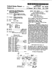
16 Claims, 4 Drawing Sheets
‘Fla
am 8115
_
q:
_|
-34
so
BUFFER
_
m
.
Aonatss
AO-AIS
|, us
_
['16 <22.
‘
WE
5|‘
CONTROL
L
cmcun
58
L
/32
nctliiiv
_> new
urrtn
cu
‘as
comm
_n
m-ms
1|
BUFFER
[2°
M15
m
m m
40
-
_
mt
m
n
Ill-113
22
24
I_
comma
2a
,
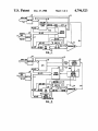
US. Patent
‘
um BUS
Dec. 27, 1988
BUFFER'] L>
H2
Sheet 1 of 4
Pm
cPu AND
@3055? ICONTROL LINES
as I“;
‘H6
cm: C
‘~26
AO-MS
Agggcss /'5
l4
4,794,523
AO-AIS
nEuoRv
{Zaumr ~n
mm
28
Al2- M5
FlG._l
'8
om BUS
‘
A9
J
'54
,so
H2 W l—>
CPU
['6
AF AIS
C;
l4. ADDRESS
BUS BUFFER
['5 { p"
"Em"
“M
95g
03£§58L q
L38
cmcun
R"
,32
CONTROL
AO-AIS
AlZ-AIS
'
aurrsa
[20
M5 mm, m
24
‘K22
2- l5
_‘ 40 win
m-ns
FIG._2.
m-ns “mm
an
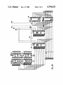
US. Patent
Dec. 27, 1988
Sheet 2 of4
4,794,523
HOSSJOOHdOUOIH
US. Patent
Dec. 27, 1988
3
Sheet 3 0f 4
4,794,523
US. Patent
Dec. 27, 1988
Sheet 4 of 4
4,794,523
1
4,794,523
2
invention is plugged into a computer, the microproces
sor resident in the computer will be disabled by the
power-up of the board of' the present invention. Since
CACHE MEMORY ARCHITECTURE FOR
MICROCOMPUTER SPEED-UP BOARD
only small portions of the software are cached at any
BACKGROUND OF THE INVENTION
5 one time, the cache memory can be a small fraction of
the size of main memory, thereby reducing its cost.
The present invention relates to fast add-on memory
Each byte of software placed in the cache memory is
for microcomputers.
tagged with a byte in the tag RAM. The byte in the tag
Cache memory is a computer memory design concept
which has been used for mainframe computers for sev- lo RAM records which section of main memory it came
from. Thus, for example, where the cache memory has
eral years. The concept is to have two separate memo
4K, the main memory is divided into 4K blocks with a
ries for the same machine, a main memory which is
large and medium speed and a cache memory which is
4K tag RAM simply recording which of the 4K blocks
small and fast. The software is loaded into the main
a particular address in the cache memory came from.
memory and then sections of it are loaded into the cache
When the microprocessor addresses the next byte of
memory as required for the central processing unit
instruction to execute, a cache memory control logic
(CPU) to process. The purposes of this arrangement is
?rst checks the tag RAM to determine if the byte to be
to increase the processing speed of the computer with
fetched is in cache memory. If it is, the byte is executed
out requiring the entire main memory to be of high
from the cache memory at high-speed. If it is not, the
speed which can be very expensive. The cache memory
microprocessor is shifted to a low speed to execute the
in such mainframe computers are typically hard-wired 20 instruction out of main memory, while simultaneously
into the computer and the internal CPU decides which
copying it into the cache RAM.
operations should use cache memory and which opera
This caching process means that when the processor
tions should use the slower main memory.
is to make, say, ten iterations through a loop that is not
Speed-up memory cards have been designed for mi
in cache memory, the ?rst iteration will be executed
crocomputers which have a high-speed processor and
from a main memory at slow speed and the successive
high-speed random access memory (RAM). Such cards
nine iterations will be executed from a cache memory at
have served to disable the processor in the microcom
high-speed.
Thus, the execution speed of software using
puter and replace the processor and RAM in the mi
the present invention will vary depending upon how the
crocomputer with that on the memory card. However,
software is designed. If the software consists of often
repeated loops, most execution time will be from a
cache memory at high-speed. Typical software execu
high-speed RAM.
tion spends approximately 80% of its time executing out
SUMMARY OF THE INVENTION
of cache memory.
The present invention is a method and apparatus for 35 The present invention also contains write-through
logic which allows an address to be written to be stored
enhancing the speed of operation of a computer. A
in a buffer at high-speed and thereafter entered into
cache memory which is faster than the main memory of
main memory at slow speed speed without slowing
a computer is provided. A portion of the program
down the operation of the fast microprocessor. The
stored in the main memory is stored in the cache mem
ory. The addresses of the portion of the main memory 40 main microprocessor of the computer is also uniquely
the replacing of the entire memory with high-speed
30
RAM can be very expensive due to the cost of such
stored in the cache memory are noted in a tag RAM.
disabled through use of the direct memory access
Upon each addressing sequence during the execution of
(DMA) line which is activated to inhibit the main mi~
croprocessor and take over operation of the computer.
a program, the tag RAM is examined to determine if the
The present invention can be applied to many differ
addressed location is stored in the cache memory. If the
stored location is identi?ed in the tag RAM, it is re 45 ent microcomputers, including the IBM and APPLE
microcomputers. The APPLE microcomputer contain
trieved from the cache memory at high-speed. Other
“soft switches” which are combinations or codes of
wise, the data in the address location is retrieved from
certain addresses which indicate that certain locations
main memory at a slower speed and written into the
cache memory so that subsequent accesses may be made
are to be accessed. The soft switches determine how
at high-speed.
In the normal operation of any microcomputer, the
50 and which memory is to be accessed. For example, the
age into the computer's memory (called “main mem
computer may have ROM and RAM which reside at
the same memory address. A soft switch will determine
if the processor is to access the ROM or the RAM.
cry”). The microprocessor on the computer then begins
Accordingly, by using programmable array logic
software to be executed is down-loaded from disc stor
to execute the software out of main memory with the 55 (PAL), these codes can be decoded to provide indica
speed of execution controlled by the speed of the micro
tion of which memory location is to be accessed and
processor, which is in turn controlled by a clock signal.
The clock signal speed is set so that it will not exceed
cached. This decoded value is then stored in the tag
RAM along with the identification of the 4K block in
the operating speed of the logic and memory chips in
memory. When soft switches are turned on and off, the
PAL circuitry mirrors this information so that the
speed-up card knows the current mode of the computer.
the computer. For economy of costs microcomputers
do not use the fastest chips available for the main mem
ory.
The cache memory design of the present invention
The present invention, through its unique ability to
disable the main microprocessor using the DMA line
utilizes a high-speed microprocessor and high-speed
and its use of the tag RAM, is able to provide fast opera
memory. Small portions of the software from main 65 tion using only a small high-speed memory. Thus, the
memory are copied into the cache memory which are
large expense of replacing the entire main memory with
then executed from cache memory using the high-speed
high-speed memory as in prior art memory speed-up
microprocessor. When a card containing the present
cards is avoided.
3
4,794,523
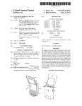
BRIEF DESCRIPTION OF THE DRAWINGS
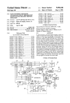
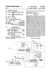
FIG. 1 is a block diagram of a preferred embodiment
4
as the IBM microcomputers, instead of a bank switch
control 40, additional tag RAM 20 is provided to cover
all the address locations. The operation of the system of
FIG. 2 is otherwise as set forth for the system of FIG.
FIG. 2 is a block diagram of the embodiment of FIG. 5 1.
FIGS. 3A-3C are schematic diagrams of a circuit
1 adapted for an APPLE computer; and
implementing the embodiment of FIG. 2. A fast micro
FIGS. 3A-3C are schematic diagrams of the embodi
processor 42 has its data lines coupled to a fast internal
ment of FIG. 2.
data bus 43 for data bits DATO-DAT7. This internal
DETAILED DESCRIPTION OF THE
data bus is coupled through registers 44, 46 to the
of the present invention;
PREFERRED EMBODIMENTS
slower main microcomputer bus on the APPLE com
puter for data bits D0-D7. Register 44 is used to buffer
information coming from the slower bus to the internal
bus, while register 46 is used to buffer data going from
the fast internal bus to the slower external bus. The
bus 12 and an address bus 14. A cache memory 16 re
internal data bits DATE-DAT? are also coupled to the
ceives addresses from bus 14 through a buffer 15 and
data inputs of the fast cache RAM’s 48 and 50.
data from data bus 12 through a buffer 18. A tag RAM
The addresses of microprocessor 42 are coupled to a
20 is addressed by address bits Ali-A10 from address
fast internal address bus 52 for address bits ADO-ADIS.
bus 14 and stores address bits A12-A15 which are input
through a buffer 22. The address bits A12-A15 stored at 20 Fast address bus 52 is coupled to the address inputs of
cache RAM’s 48 and 50. The fast address bus 52 is
a particular location in tag RAM are compared with
coupled to the slower main microcomputer bus 54 for
bits A12-A15 of a current address by a comparator 24.
address bits All-A15 by registers 56, 58 and latches 60,
CPU 10 controls the operation of the various compo
62.
nents of the board through a number of control lines 26.
In operation, after the board of the present invention 25 The remaining circuitry of FIG. 3A provides the
various clock and timing signals through the use of a
is plugged into a computer, it is powered up and dis
number of ?ip-?ops and gates and PAL’s 64 and 66.
ables the computer’s main microprocessor. Instructions
Referring to FIG. 3C, tag RAM’s 68 and 70 are pro
are then executed at fast speed using a fast microproces
vided with data through a buffer 72. Address bits ADI
sor in CPU 10. Whenever an address appears on address
2-AD15 of the current address and soft switch mode
bus 14, bits All-A10 of that address are input to tag
signals Model-Mode3 for the current address are com
RAM 20 which produces an output to comparator 24
pared to the contents of RAM’s 68 and 70 (address bits
consisting of the bits A12-A15 stored in the tag RAM.
A12-A15 and Model-Mode3) in comparator 74. PAL’s
These bits A12-A15 identify the particular 4K block of
76, 78 and 80 decode the current address to produce a
memory which is stored in cache memory 16. If this 4K
block does not match the 4K block identi?ed by address 35 three-bit signal (Model-Mode3) on lines 82 based on
the current soft switch settings.
bits A12-A15 of the current address, comparator 24
FIG. 1 is a block diagram of a preferred embodiment
of a memory speed-up board according to the present
invention. CPU and control logic 10 is coupled to a data
would indicate no match on output line 28 to CPU 10.
CPU 10 will then switch to a slow speed and access the
In operation, on power-up, a ROM 84 does a dummy
read to validate the system and fill the cache RAM with
address from the computer's main memory. This ad
dress will then be stored in cache memory 16 and the
4K block identifying its location will be stored in tag
RAM 20. The next time this particular address is exe
cuted, comparator 24 would indicate that it is stored in
known values. If requested by the user, it also performs
a self-test transfer from the APPLE minicomputer main
memory and the APPLE resident ROM (read-only
cache memory and CPU 10 will execute such address
out of cache memory 16 at high-speed.
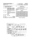
FIG. 2 is a block diagram of the embodiment of FIG.
1 adapted for an APPLE microcomputer. In addition to
the elements of FIG. 1, a speed control circuit 30 and a
cache memory control circuit 32 have been separated
out from CPU 10 of FIG. 1 and perform the functions of 50
the control logic in CPU 10 of FIG. 1. Speed control
circuit 30 provides a clock signal 36 determining the
microprocessor speed. CPU 34 provides a read/write
signal 38 to cache memory control circuit 32. Speed
memory) and then disables itself and turns over control
to microprocessor 42.
PAL circuits 76, 78 and 80 of FIG. 3C perform a
straightforward decoding of the soft switches in the
addresses. A signal RWN to PAL 76 is activated for
certain APPLE addresses which are only meaningful
when written to. An output signal TGO produced by
PAL 80 is used for disk access which requires system
operation to slow down. A one-shot 86 in FIG. 3A
provides the required 15 millisecond (ms) delay. An
output signal MENABB from PAL 80 indicates that the
address decoded should not be read out of cache
RAM’s 48 and 50 because it corresponds to an I/O
control circuit 30 and cache control circuit 32 then 55 (input/output) slot or other memory which should not
control the operation of the remaining elements of the
system.
be cached (for example, bank switched memory as the
tag cannot maintain the bank). Because it is an [/0 slot,
its contents might change and the cache RAM would
A bank switch control 40 is provided to receive ad
not be aware of this change. Therefore, it must be up
dresses A0—A15 and to decode the addresses to produce
a three-bit word M1-M3, which, in conjunction with 60 dated for every addressing. A signal ROMEN input to
PAL 80 and to ROM 84 is used to activate the ROM
the current soft switch settings, determine the exact
and deactivate PAL 80 upon power-up.
source of a single byte of memory. Such a soft switch is
Referring now to FIG. 3A, registers 56, 58 and
a particular address which indicates that a particular
latches 60, 62 allow data to be written to the latches at
memory location of the main memory is to be accessed,
i.e., auxiliary memory, ROM, RAM, etc. This addi
tional address information M1-M3 is also processed
through buffer 22 and stored in tag RAM 20. For a
microcomputer which does not use soft switches, such
high-speed with microprocessor 42 continuing on to the
next instruction. Thereafter, the system can at its lei
sure, at the slower l-megahertz (MI-Iz) APPLE speed,
write the data to the APPLE computer's main memory.
5
4,794,523
Microprocessor 42 will normally operate at 3.5 MHz,
thereby giving it an optimum 3.5 times speed increase
over the APPLE computer's resident microprocessor.
TABLE I-continued
PAL Control Signals
data lines. Allows the Direct Memory Access
line (pin 22) on the APPLE bus to ?oat high
enabling the APPLE's normal 6502 microproces
sor to operate. Any time pin 22 is low, the
Depending on how the software is written and how
often repeat loops are performed, the execution speed
will more typically be between 2.5 and 3.2 times faster
than the normal APPLE execution speed.
The PAL’s and the logic circuits of FIG. 3B provide .r
the timing and control signals for the system. The func—
tons of the signals operated on and produced by PAL's 10
APPLE 6052 is completely disabled, ?oating
all of its address and data lines which is
the method in which the present system takes
control of the APPLE.
This signal takes the place of the normal
APPLE WR' signal (pin 18 on the APPLE bus).
64, 66 are set forth in Table I below.
When an actual write to the APPLE bus occurs,
TABLE I
this signal drops low. This signal is dis
PAL Control Signals
abled when DMA is not asserted.
ROM Enable: The presence of ROM 84 is indi
PAL 64
Processor Clock. Depending on the mode of
cated by the assertion of this signal and is
only present while the system is determining
the mode of operation. It disallows the sys
the system (high speed or synchronous with
slower APPLE clock) this clock will ?uctuate
tem to cache memory from the high address
between 1 MHz and 3.59 MHz.
WRT:
CEN:
Cache write signal. how when writing to Cache
memory 48, 50.
TAG:
space which is where the ROM image is initially
located (thus overlaying the APPLE operating
20
system ROM's). This is necessary since the
cache RAM is unde?ned upon power-up and it
Cache output enable. Low when processor 42
is reading Cache memory 48, 50.
External Write signal. Asserted when a write
to the APPLE bus 47 is required. Propagates
through to PALX where the actual APPLE write
is synchronized. This signal initiates the process.
Cache tag signal. This signal is asserted
allows the power-up software to define all of
the cache before normal operation. After the
cache initialization, the system creates a
copy of itself in normal APPLE RAM at address
25
$1000 (hex) and transfers execution to there.
Normal operation starts, and this signal is
asserted false, thus allowing the system to
cache high memory.
Data Bus Buffer Output Enable: This signal
enables the data bus output buffers 44, 46
when cache RAM 48, 50 is written to.
CRD:
Cache read signal. This signal is asserted
when cache RAM 48, 50 is read from.
Timing signal ?ip-?op. This signal, combined
with FFl, stops and starts PCK for transitions
CLR:
between synchronous 1 MHz operation and asyn
chronous 3.59 MHz operation.
BRE:
Initiates slow down of PCK from 3.59 MHz to 1
MHz. Also latches address and data into but‘
fers 56, S8 and 46 for writes to the APPLE
bus 47, 54 which are later enabled onto the
OAN:
APPLE bus during the next phase 0 clock cycle.
If data is latched into the ?rst stage but‘
35
FFl :
7MN:
EXW:
FFO:
RST:
fers 56, 58 and 46 and a subsequent write
occurs before the next phase 0. the processor
will stop until the next phase 0 before CLR
Used for synchronization during clock changes.
INQ:
DL2 are of the same state. when the clock
rate is to change, these two signals will
CRD:
l/OSTRB‘ signal from APPLE bus. REN is enabled
by a reset and is held until this signal appears.
Allows signals to be generated. When the
system is disabled, this signal is asserted
low causing outputs from this PAL to the APPLE
bus to stop.
Latched version of CRD from PAL 64. Causes
OON:
generation of read signals from this PAL 66
and is latched through by the 4MN clock.
Inverted phase 0 from APPLE bus.
DMA:
sequentially change states Other signals in
the PAL‘s look at these two signals to deter
DLZ:
DAN:
7MN:
the APPLE bus 47, 54.
See DLI.
operations.
I-ILD:
45
Same as DAN on PAL 66.
Inverted 7.18 MHz clock from the APPLE bus.
This clock is divided by two internally pro
ducing the 3.59 MHz clock used for high-speed
When CLR is generated, HLD holds CLR for one
from the APPLE bus, this signal enables the
output buffer.
Maser Asynchronous 3.59 MHz clock which is
derived by dividing the APPLE 7.18 MHz clock by 2.
See FFl of PAL 64.
See 'IMN of PAL 64.
See EXW of PAL 64.
See FFO of PAL 64.
Reset signal from APPLE bus. Causes the sys~
to initialize the cache memory.
No signals may be generated unless DH and
mine whether writes/reads are out of cache or
for writes to the APPLE bus 47.
Data Bus Buffer Read Output Enable: For reads
tem to begin reading its on-board ROM 84 with
out caching memory, thus enabling the software
can latch the new data into the buffer.
DLl:
6
50 Al I:
CFD:
Inverted Address line ll from microprocessor 42.
When gated with EXW generates a timing pulse
for system disable.
following phase 0 clock cycle.
4M:
High speed clock. This is the divided by two
versions of 7MN described above. ms is
actually a misnomer since the actual frequency
present at this pin is 3.59 MHz.
RWN:
FFI:
MCH:
Read/W rite signal output from microprocessor 42.
See FFO.
Match signal from comparator 74. This signal
is asserted low by the comparator whenever
tag memory 68, 70 matches the current requested
memory byte. It‘ the tag bits match, MCH may
still be disabled if the location is not a
valid cache location as determined by MENABN
ZMN:
produced by MEN of PAL 80.
Used for proper synchronization of DLl and DLZ.
PAL 66
Clock for disabling the system. This signal
gates the BDDIS' signal from PAL 78 into a
latch which completely removes the system
from operation thus releasing all address and
As will be understood by those familar with the art,
55 the present invention may be embodied in other speci?c
forms without departing from the spirit or essential
characteristics thereof. FIGS. 2 and 3 show a speci?c
embodiment for an APPLE microcomputer. Other
embodiments could implement the system of FIG. 1 for
IBM or other microcomputers. Accordingly, the disclo
sure of the preferred embodiment of the invention is
intended to be illustrative, but not limiting, of the scope
of the invention which is set forth in the following
claims.
65
What is claimed is:
1. A method for enhancing the speed of operation of
a computer having a plurality of devices including a
?rst microprocessor coupled to a main memory via an
7
4,794,523
address bus, said computer being designed to operate at
a ?rst clock cycle time, comprising the steps of:
address bus, said computer being designed to operate at
a ?rst clock cycle time, comprising the steps of:
providing a cache memory having a faster access
time than an access time of said main memory used
providing a cache memory having a faster access
time than an access time of said main memory used
by said computer;
permanently disabling or disconnecting said ?rst mi
by said computer;
permanently disabling or disconnecting said ?rst mi
croprocessor on or before power-up;
producing a second clock having a faster cycle time
than said ?rst clock cycle time;
providing a second microprocessor operating at said
second clock cycle time;
storing a portion of the data of said main memory in
said cache memory;
intercepting an addressing of a location in said main
memory on said address bus by said fast micro
processor;
producing a signal designating one of a plurality of
banks of said main memory in response to the ad
dressing of a location in said main memory by said
croprocessor on or before power-up;
producing a second clock having a faster cycle time
than said ?rst clock cycle time;
providing a second microprocessor operating at said
second clock cycle time;
storing a portion of the data of said main memory in
said cache memory;
intercepting an addressing of a location in said main
memory on said address has by said fast micro
processor;
producing a signal designating one of a plurality of
banks of said main memory in response to the ad
dressing of a location in said main memory by said
second microprocessor, each of said banks using 20
second microprocessor, each of said banks using
the same addresses from said second microproces
the same addresses from said second microproces
901’;
determining, in response to said addressing of a loca
tion in said main memory, whether the data of said
25
location is stored in said cache memory;
retrieving said data for said fast microprocessor from
said cache memory at said faster access time if said
data are determined to be in said cache memory;
and
communicating with said plurality of devices, exclud
ing said ?rst microprocessor, at said ?rst clock
cycle time.
2. The method of claim 1 wherein said determining
step comprises the steps of:
storing, in a tag memory, a ?rst portion of each of 35
said main memory addresses for data also stored in
said cache memory, said data being stored in said
cache memory at a location in said cache memory
corresponding to a second portion of said main
40
memory address; and
comparing a ?rst portion of a current address to said
address ?rst portion stored in said tag memory.
3. The method of claim 1 wherein said data is stored
in said cache memory upon a ?rst request for said data.
4. The method of claim 3 further comprising the step 45
of eliminating an earlier byte of data stored in a cache
memory location upon a request for a byte of data after
said cache memory location is ?lled.
5. The method of claim 1 wherein said disabling step
comprises providing a signal to a direct memory access 50
line of said computer.
6. The method of claim 1 further comprising the steps
Of:
decoding an address to determine the location of said
55
address; and
providing a clock speed for said second microproces
sor compatible with said location.
7. The method of claim 1 further comprising the steps
of:
storing an element of data to be written into said main
memory in a buffer during a clock cycle corre
sponding to said faster access time; and
subsequently writing said element of data into said
main memory during a slower clock cycle indepen
65
dent of said faster access clock cycle.
8. A method for enhancing the speed of operation of
a computer having a plurality of devices including a
?rst microprocessor coupled to a main memory via an
sor;
storing, in a tag memory, a ?rst portion of each of the
main memory addresses for data also stored in said
cache memory, said data being stored in said cache
memory at a location in said cache memory corre
sponding to a second portion of said main memory
address;
comparing a ?rst portion of a current address to said
address ?rst portion stored in said tag memory;
retrieving said data from said cache memory if said
compared addresses are identical; and
communicating with said plurality of devices, exclud
ing said ?rst microprocessor, at said ?rst clock
cycle time.
9. An apparatus for enhancing the speed of operation
of a computer having a plurality of devices including a
?rst microprocessor and a main memory, said computer
being designed to operate at a ?rst clock cycle time,
comprising:
means for coupling said apparatus to address and data
lines coupled to said ?rst microprocessor and per
manently disabling said ?rst microprocessor on or
before power-up;
means for communicating with said plurality of de
vices, excluding said ?rst microprocessor, at said
?rst clock cycle time;
means for producing a second clock having a faster
cycle time than said ?rst clock cycle time;
a cache memory having a faster access time than an
access time of said main memory used by said com
puter;
a second microprocessor operating at said second
clock cycle time;
means for storing a portion of the data of said main
memory in said cache memory;
means for producing a signal designating one of a
plurality of banks of said main memory in response
to the addressing of a location in said main memory
by said second microprocessor, each of said banks
using the same addresses from said second micro
processor;
means for determining, in response to the addressing
of a location in said main memory by said second
microprocessor, whether the data of said location
is stored in said cache memory; and
means for retrieving said data for said second micro
processor i'rom said cache memory using said sec
9
4,794,523
10
means for coupling said apparatus to a ?rst address
bus and ?rst data bus coupled to said ?rst micro
and clock if said data are determined to be in said
cache memory.
10. The apparatus of claim 9 wherein said means for
processor and permanently disabling said ?rst mi
determining comprises:
croprocessor on or before power-up;
means for communicating with said plurality of de
vices, excluding said ?rst microprocessor, at said
?rst clock cycle time;
a tag memory;
means for storing in said tag memory a ?rst portion of
each of said main memory addresses for data stored
in said cache memory at a location in said cache
memory corresponding to a second portion of said
main memory address; and
means for producing a second clock having a faster
cycle time than said ?rst clock cycle time;
a second microprocessor operating at said second
clock cycle time;
means for comparing a ?rst portion of a current ad
a cache memory having a faster access time than an
dress to said address ?rst portion stored in said tag
access time of said main memory of said computer,
memory.
11. The apparatus of claim 9 wherein said data is
stored in said cache memory upon a ?rst request for said 15
data.
12. The apparatus of claim 11 further comprising
means for eliminating an earlier byte of data stored in a
cache memory location upon a request for a byte of data
20
from said main memory after said cache memory loca
tion is ?lled.
13. The apparatus of claim 9 wherein said disabling
means comprises means for providing a signal to a di
rect memory access line of said ?rst microprocessor. 25
14. The apparatus of claim 9 further comprising:
means for decoding an address from said second mi
croprocessor to determine the location of said ad
said cache memory being smaller than said main
memory;
a tag memory for storing a ?rst portion of each main
memory address for data also stored in said cache
memory, said ?rst address portion being stored in
said tag memory at an address corresponding to a
second portion of said main memory address;
a comparator for comparing a ?rst portion of a cur
rent address with a ?rst address portion stored in
said tag memory;
control means for retrieving data for said second
microprocessor from said cache memory at said
faster access time responsive to said comparator;
a fast data bus, internal to said add-on apparatus,
coupled to said second microprocessor and said
dress; and
cache memory;
a fast address bus, internal to said add-on apparatus,
means for providing an addressing sequence clock
speed for said second microprocessor compatible
coupled to said second microprocessor, said tag
memory and said comparator;
with said location.
15. The apparatus of claim 9 further comprising:
a buffer for storing an element of data to be written
into said main memory during a clock cycle corre 35
sponding to said faster access time; and
means for subsequently writing said element of data
into said main memory during a slower clock cy
cle.
16. An add-on apparatus for enhancing the speed of
operation of a computer having a plurality of devices
including a ?rst microprocessor and a main memory,
said computer being designed to operate at a ?rst clock
means for producing a signal designating one of a
plurality of banks of said main memory in response
to the addressing of a location in said main memory
by said second microprocessor, each of said banks
using the same addresses from said second micro
processor;
a ?rst buffer means for coupling said fast data bus to
said ?rst data bus of said ?rst microprocessor; and
a second buffer means for coupling said fast address
bus to said ?rst address bus of said ?rst micro
processor.
cycle time, comprising:
!
45
50
55
65
i
#
'
l