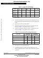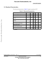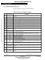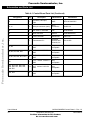
1
Freescale Semiconductor, Inc.
MC68HC908MR32
Control Board
User’s Manual
For More Information On This Product,
Go to: www.freescale.com
A G R E E M E N T
Motorola Embedded Motion Control
N O N - D I S C L O S U R E
Freescale Semiconductor, Inc...
R E Q U I R E D
MEMCMR32CBUM/D
Rev. 1.0
Freescale Semiconductor, Inc.
MC68HC908MR32 Control Board
Important Notice to Users
Freescale Semiconductor, Inc...
While every effort has been made to ensure the accuracy of all information in
this document, Motorola assumes no liability to any party for any loss or
damage caused by errors or omissions or by statements of any kind in this
document, its updates, supplements, or special editions, whether such errors are
omissions or statements resulting from negligence, accident, or any other cause.
Motorola further assumes no liability arising out of the application or use of any
information, product, or system described herein: nor any liability for incidental
or consequential damages arising from the use of this document. Motorola
disclaims all warranties regarding the information contained herein, whether
expressed, implied, or statutory, including implied warranties of
merchantability or fitness for a particular purpose. Motorola makes no
representation that the interconnection of products in the manner described
herein will not infringe on existing or future patent rights, nor do the
descriptions contained herein imply the granting or license to make, use or sell
equipment constructed in accordance with this description.
Trademarks
This document includes these trademarks:
Motorola and the Motorola logo are registered trademarks
of Motorola, Inc.
Motorola, Inc., is an Equal Opportunity / Affirmative Action Employer.
© Motorola, Inc., 2000; All Rights Reserved
User’s Manual
2
MC68HC908MR32 Control Board — Rev. 1.0
MC68HC908MR32 Control Board
For More Information On This Product,
Go to: www.freescale.com
MOTOROLA
Freescale Semiconductor, Inc.
User’s Manual — MC68HC908MR32 Control Board
List of Sections
Section 1. Introduction and Setup . . . . . . . . . . . . . . . . . . 11
Freescale Semiconductor, Inc...
Section 2. Operational Description . . . . . . . . . . . . . . . . . 21
Section 3. Pin Descriptions . . . . . . . . . . . . . . . . . . . . . . . 31
Section 4. Schematics and Parts List . . . . . . . . . . . . . . . 43
Section 5. Design Considerations . . . . . . . . . . . . . . . . . . 53
MC68HC908MR32 Control Board — Rev. 1.0
MOTOROLA
List of Sections
For More Information On This Product,
Go to: www.freescale.com
User’s Manual
3
Freescale Semiconductor, Inc.
Freescale Semiconductor, Inc...
List of Sections
User’s Manual
4
MC68HC908MR32 Control Board — Rev. 1.0
List of Sections
For More Information On This Product,
Go to: www.freescale.com
MOTOROLA
Freescale Semiconductor, Inc.
User’s Manual — MC68HC908MR32 Control Board
Table of Contents
Freescale Semiconductor, Inc...
Section 1. Introduction and Setup
1.1
Contents . . . . . . . . . . . . . . . . . . . . . . . . . . . . . . . . . . . . . . . . . . . . . . . 11
1.2
Introduction. . . . . . . . . . . . . . . . . . . . . . . . . . . . . . . . . . . . . . . . . . . . . 11
1.3
About this Manual. . . . . . . . . . . . . . . . . . . . . . . . . . . . . . . . . . . . . . . . 13
1.4
Warnings . . . . . . . . . . . . . . . . . . . . . . . . . . . . . . . . . . . . . . . . . . . . . . . 14
1.5
Setup Guide. . . . . . . . . . . . . . . . . . . . . . . . . . . . . . . . . . . . . . . . . . . . . 15
Section 2. Operational Description
2.1
Contents . . . . . . . . . . . . . . . . . . . . . . . . . . . . . . . . . . . . . . . . . . . . . . . 21
2.2
Introduction. . . . . . . . . . . . . . . . . . . . . . . . . . . . . . . . . . . . . . . . . . . . . 21
2.3
Electrical Characteristics . . . . . . . . . . . . . . . . . . . . . . . . . . . . . . . . . . 23
2.4
2.4.1
2.4.2
2.4.3
2.4.4
2.4.5
2.4.6
User Interfaces . . . . . . . . . . . . . . . . . . . . . . . . . . . . . . . . . . . . . . . . . . 24
Potentiometers . . . . . . . . . . . . . . . . . . . . . . . . . . . . . . . . . . . . . . . . 24
Switches . . . . . . . . . . . . . . . . . . . . . . . . . . . . . . . . . . . . . . . . . . . . . 24
Jumpers . . . . . . . . . . . . . . . . . . . . . . . . . . . . . . . . . . . . . . . . . . . . . 25
Indicator Lights . . . . . . . . . . . . . . . . . . . . . . . . . . . . . . . . . . . . . . . 26
Test Points . . . . . . . . . . . . . . . . . . . . . . . . . . . . . . . . . . . . . . . . . . . 27
RS-232 Interface . . . . . . . . . . . . . . . . . . . . . . . . . . . . . . . . . . . . . . 29
Section 3. Pin Descriptions
3.1
Contents . . . . . . . . . . . . . . . . . . . . . . . . . . . . . . . . . . . . . . . . . . . . . . . 31
3.2
Introduction. . . . . . . . . . . . . . . . . . . . . . . . . . . . . . . . . . . . . . . . . . . . . 31
3.3
3.3.1
3.3.2
Control Board Signal Descriptions . . . . . . . . . . . . . . . . . . . . . . . . . . . 32
Tacho Input Connector J1 . . . . . . . . . . . . . . . . . . . . . . . . . . . . . . . 32
Hall Sensor/Encoder Input Connector J2. . . . . . . . . . . . . . . . . . . . 33
MC68HC908MR32 Control Board — Rev. 1.0
MOTOROLA
Table of Contents
For More Information On This Product,
Go to: www.freescale.com
User’s Manual
5
Freescale Semiconductor, Inc.
Freescale Semiconductor, Inc...
Table of Contents
3.3.3
3.3.4
3.3.5
3.3.6
3.3.7
40-Pin Emulator Connector J3 . . . . . . . . . . . . . . . . . . . . . . . . . . . . 34
40-Pin Emulator Connector J4 . . . . . . . . . . . . . . . . . . . . . . . . . . . . 36
40-Pin Connector J5. . . . . . . . . . . . . . . . . . . . . . . . . . . . . . . . . . . . 38
RS-232 DB-9 Connector J6 . . . . . . . . . . . . . . . . . . . . . . . . . . . . . . 41
Power Connector J7 . . . . . . . . . . . . . . . . . . . . . . . . . . . . . . . . . . . . 41
3.4
3.4.1
3.4.2
Daughter Board Signal Descriptions . . . . . . . . . . . . . . . . . . . . . . . . . 42
Daughter Board Connector J1 . . . . . . . . . . . . . . . . . . . . . . . . . . . . 42
Daughter Board Connector J2 . . . . . . . . . . . . . . . . . . . . . . . . . . . . 42
Section 4. Schematics and Parts List
4.1
Contents . . . . . . . . . . . . . . . . . . . . . . . . . . . . . . . . . . . . . . . . . . . . . . . 43
4.2
Overview. . . . . . . . . . . . . . . . . . . . . . . . . . . . . . . . . . . . . . . . . . . . . . . 43
4.3
Schematics . . . . . . . . . . . . . . . . . . . . . . . . . . . . . . . . . . . . . . . . . . . . . 43
4.4
Parts Lists . . . . . . . . . . . . . . . . . . . . . . . . . . . . . . . . . . . . . . . . . . . . . . 49
Section 5. Design Considerations
User’s Manual
6
5.1
Contents . . . . . . . . . . . . . . . . . . . . . . . . . . . . . . . . . . . . . . . . . . . . . . . 53
5.2
Overview. . . . . . . . . . . . . . . . . . . . . . . . . . . . . . . . . . . . . . . . . . . . . . . 53
5.3
Sensor Inputs. . . . . . . . . . . . . . . . . . . . . . . . . . . . . . . . . . . . . . . . . . . . 54
5.4
Simultaneous Conduction Lockout. . . . . . . . . . . . . . . . . . . . . . . . . . . 55
5.5
Dead Time. . . . . . . . . . . . . . . . . . . . . . . . . . . . . . . . . . . . . . . . . . . . . . 55
5.6
Power-Up/Power-Down . . . . . . . . . . . . . . . . . . . . . . . . . . . . . . . . . . . 55
5.7
Grounding . . . . . . . . . . . . . . . . . . . . . . . . . . . . . . . . . . . . . . . . . . . . . . 56
5.8
Fault Circuits. . . . . . . . . . . . . . . . . . . . . . . . . . . . . . . . . . . . . . . . . . . . 56
5.9
Tachometer Input . . . . . . . . . . . . . . . . . . . . . . . . . . . . . . . . . . . . . . . . 58
5.10
Optoisolated RS-232 Interface . . . . . . . . . . . . . . . . . . . . . . . . . . . . . . 58
5.11
Back EMF Signals . . . . . . . . . . . . . . . . . . . . . . . . . . . . . . . . . . . . . . . 60
MC68HC908MR32 Control Board — Rev. 1.0
Table of Contents
For More Information On This Product,
Go to: www.freescale.com
MOTOROLA
Freescale Semiconductor, Inc.
User’s Manual — MC68HC908MR32 Control Board
List of Figures
Freescale Semiconductor, Inc...
Figure
Title
1-1
1-2
1-3
1-4
1-5
Systems’ Configurations. . . . . . . . . . . . . . . . . . . . . . . . . . . . . . . . . . . 13
Control Board Photograph . . . . . . . . . . . . . . . . . . . . . . . . . . . . . . . . . 16
Setup Parts Locations . . . . . . . . . . . . . . . . . . . . . . . . . . . . . . . . . . . . . 16
Setup for High-Voltage Systems . . . . . . . . . . . . . . . . . . . . . . . . . . . . 17
Setup for Low-Voltage Systems . . . . . . . . . . . . . . . . . . . . . . . . . . . . . 19
2-1
Block Diagram . . . . . . . . . . . . . . . . . . . . . . . . . . . . . . . . . . . . . . . . . . 22
3-1
3-2
Connector Parts Locations . . . . . . . . . . . . . . . . . . . . . . . . . . . . . . . . . 32
40-Pin Ribbon Cable Connector J5. . . . . . . . . . . . . . . . . . . . . . . . . . . 38
4-1
4-2
4-3
4-4
4-5
Daughter Board. . . . . . . . . . . . . . . . . . . . . . . . . . . . . . . . . . . . . . . . . . 44
Connectors J3 and J4 . . . . . . . . . . . . . . . . . . . . . . . . . . . . . . . . . . . . . 45
Control Board Schematic (Sheet 1) . . . . . . . . . . . . . . . . . . . . . . . . . . 46
Control Board Schematic (Sheet 2) . . . . . . . . . . . . . . . . . . . . . . . . . . 47
Control Board Schematic (Sheet 3) . . . . . . . . . . . . . . . . . . . . . . . . . . 48
5-1
5-2
5-3
5-4
5-5
Hall Sensor Inputs. . . . . . . . . . . . . . . . . . . . . . . . . . . . . . . . . . . . . . . . 54
Fault Circuits. . . . . . . . . . . . . . . . . . . . . . . . . . . . . . . . . . . . . . . . . . . . 57
Tachometer Input . . . . . . . . . . . . . . . . . . . . . . . . . . . . . . . . . . . . . . . . 58
RS-232 Interface . . . . . . . . . . . . . . . . . . . . . . . . . . . . . . . . . . . . . . . . . 58
Zero Cross Back EMF Circuit . . . . . . . . . . . . . . . . . . . . . . . . . . . . . . 60
MC68HC908MR32 Control Board — Rev. 1.0
MOTOROLA
Page
List of Figures
For More Information On This Product,
Go to: www.freescale.com
User’s Manual
7
Freescale Semiconductor, Inc.
Freescale Semiconductor, Inc...
List of Figures
User’s Manual
8
MC68HC908MR32 Control Board — Rev. 1.0
List of Figures
For More Information On This Product,
Go to: www.freescale.com
MOTOROLA
Freescale Semiconductor, Inc.
User’s Manual — MC68HC908MR32 Control Board
List of Tables
Freescale Semiconductor, Inc...
Table
Title
1-1
1-2
Jumper JP1–JP5 Settings . . . . . . . . . . . . . . . . . . . . . . . . . . . . . . . . . . 18
Overcurrent and Overvoltage Adjustments . . . . . . . . . . . . . . . . . . . . 18
2-1
2-2
2-3
Electrical Characteristics . . . . . . . . . . . . . . . . . . . . . . . . . . . . . . . . . . 23
Timer Channel Configuration . . . . . . . . . . . . . . . . . . . . . . . . . . . . . . . 26
Test Points . . . . . . . . . . . . . . . . . . . . . . . . . . . . . . . . . . . . . . . . . . . . . 27
3-1
3-2
3-3
3-4
3-5
3-6
Hall Sensor Input . . . . . . . . . . . . . . . . . . . . . . . . . . . . . . . . . . . . . . . . 33
Quadrature Encoder Input. . . . . . . . . . . . . . . . . . . . . . . . . . . . . . . . . . 33
Connector J3 Signal Descriptions . . . . . . . . . . . . . . . . . . . . . . . . . . . 34
Connector J4 Signal Descriptions . . . . . . . . . . . . . . . . . . . . . . . . . . . 36
Connector J5 Signal Descriptions. . . . . . . . . . . . . . . . . . . . . . . . . . . . 39
Connector J6 Signal Descriptions . . . . . . . . . . . . . . . . . . . . . . . . . . . 41
4-1
4-2
Control Board Parts List . . . . . . . . . . . . . . . . . . . . . . . . . . . . . . . . . . 49
Daughter Board Parts List . . . . . . . . . . . . . . . . . . . . . . . . . . . . . . . . . 51
MC68HC908MR32 Control Board — Rev. 1.0
MOTOROLA
Page
List of Tables
For More Information On This Product,
Go to: www.freescale.com
User’s Manual
9
Freescale Semiconductor, Inc.
Freescale Semiconductor, Inc...
List of Tables
User’s Manual
10
MC68HC908MR32 Control Board — Rev. 1.0
List of Tables
For More Information On This Product,
Go to: www.freescale.com
MOTOROLA
Freescale Semiconductor, Inc.
User’s Manual — MC68HC908MR32 Control Board
Section 1. Introduction and Setup
Freescale Semiconductor, Inc...
1.1 Contents
1.2
Introduction. . . . . . . . . . . . . . . . . . . . . . . . . . . . . . . . . . . . . . . . . . . . . 11
1.3
About this Manual. . . . . . . . . . . . . . . . . . . . . . . . . . . . . . . . . . . . . . . . 13
1.4
Warnings . . . . . . . . . . . . . . . . . . . . . . . . . . . . . . . . . . . . . . . . . . . . . . . 14
1.5
Setup Guide. . . . . . . . . . . . . . . . . . . . . . . . . . . . . . . . . . . . . . . . . . . . . 15
1.2 Introduction
Motorola’s MC68HC908MR32 motor control board is an integral part of the
embedded motion control series of development tools. It interfaces easily with
power stages, optoisolators, and emulators to complement software
development tools for the MC68HC908MR32 (MR32).
The MR32 motor control board is supplied in kit number ECCTR908MR32. It
is shipped along with a small printed circuit daughter board (SKT908MR32),
an MR32, a 12-volt/4-amp power supply, mounting hardware, a 40-pin ribbon
cable, and a CD ROM.
The MR32 motor control board is designed as an aid for hardware and software
development of 3-phase ac induction, brushless dc (BLDC), and switched
reluctance (SR) motor drives.
There are two modes of operation.
•
The MR32 control board can be connected to an M68EM08MR32
emulator board, in an MMDS05/08 or MMEVS05/08 emulation system,
through an M68CBL08A impedance-matched ribbon cable.
•
Alternatively, the daughter board housing an HC908MR32 can be
plugged into the control board in place of the emulator cable from the
MMDS08.
MC68HC908MR32 Control Board — Rev. 1.0
MOTOROLA
Introduction and Setup
For More Information On This Product,
Go to: www.freescale.com
User’s Manual
11
Freescale Semiconductor, Inc.
Introduction and Setup
Freescale Semiconductor, Inc...
A few of the more noteworthy features are:
•
Six motor control PWM outputs with LED indicators
•
Speed control potentiometer
•
Optoisolated half-duplex RS-232 interface
•
Start/Stop and Forward/Reverse switches
•
Hall effect inputs for brushless dc motor control
•
Back EMF inputs for brushless dc motor control
•
Tachometer input
•
2-position DIP switch for user option control
•
Emulator/Daughter board connectors
•
Processor reset switch
•
Two system fault inputs
•
Nine analog inputs
•
Three softwarecontrolled LEDs
•
Regulated on-board regulated power supply
The MR32 motor control board fits into the systems’ configurations that are
shown in Figure 1-1. A photograph of the control board with its daughter board
attached appears in Figure 1-2.
User’s Manual
12
MC68HC908MR32 Control Board — Rev. 1.0
Introduction and Setup
For More Information On This Product,
Go to: www.freescale.com
MOTOROLA
Freescale Semiconductor, Inc.
Introduction and Setup
About this Manual
EMULATOR
CONTROL BOARD
CONTROL BOARD
WORKSTATION
WORKSTATION
LOW-VOLTAGE
POWER BOARD
Freescale Semiconductor, Inc...
EMULATOR
OPTOISOLATION
BOARD
HIGH-VOLTAGE
POWER BOARD
MOTOR
OPTIONAL FEEDBACK
MOTOR
OPTIONAL FEEDBACK
a) LOW VOLTAGE
b) HIGH VOLTAGE
Figure 1-1. Systems’ Configurations
1.3 About this Manual
Key items can be found in the following locations in this manual:
•
Setup instructions are found in 1.5 Setup Guide.
•
Schematics are found in 4.3 Schematics.
•
Pin assignments are shown in Figure 3-2. 40-Pin Ribbon Cable
Connector J5, and a pin-by-pin description is contained in 3.3 Control
Board Signal Descriptions.
•
For those interested in the reference design aspects of the board’s
circuitry, a description is provided in Section 5. Design Considerations.
MC68HC908MR32 Control Board — Rev. 1.0
MOTOROLA
Introduction and Setup
For More Information On This Product,
Go to: www.freescale.com
User’s Manual
13
Freescale Semiconductor, Inc.
Introduction and Setup
1.4 Warnings
This development tool set operates in an environment that can include
dangerous voltages and rotating machinery.
To facilitate safe operation, input power for high-voltage power stages should
come from a current-limited dc laboratory power supply, unless power factor
correction is specifically being investigated.
Freescale Semiconductor, Inc...
When operating high-voltage power stages directly from an ac line, power stage
grounds and oscilloscope grounds are at different potentials, unless the
oscilloscope is floating. Note that probe grounds and, therefore, the case of a
floated oscilloscope, are subjected to dangerous voltages.
The user should be aware that:
User’s Manual
14
•
Before moving scope probes, making connections, etc., it is generally
advisable to power down the high-voltage supply.
•
When high voltage is applied to one of the high-voltage power stages,
using only one hand for operating the test setup minimizes the possibility
of electrical shock.
•
Operation in labs with grounded tables and/or chairs should be avoided.
•
Wearing safety glasses, avoiding ties and jewelry, using shields, and
operation by personnel trained in high-voltage lab techniques are also
advisable.
MC68HC908MR32 Control Board — Rev. 1.0
Introduction and Setup
For More Information On This Product,
Go to: www.freescale.com
MOTOROLA
Freescale Semiconductor, Inc.
Introduction and Setup
Setup Guide
1.5 Setup Guide
Freescale Semiconductor, Inc...
Setup and connections for the MR32 motor control board are very
straightforward. Input connections to an M68EM08MR32 emulator are made
through an M68CBL08A impedance-matched ribbon cable. Output
connections to an embedded motion control optoisolation board or low-voltage
power stage are made via a 40-pin ribbon cable that is supplied in the
ECCTR908MR32 kit. The MR32 motor control board is powered through the
40-pin ribbon cable, regardless if it is connected to the optoisolation board or a
low-voltage power stage. The included 12-volt/4-amp power supply provides
power for either the optoisolation board or a low-voltage power stage.
Figure 1-3 shows parts locations, and Figure 1-4 depicts a completed
high-voltage setup.
A step-by-step procedure for setup with an optoisolator board and high-voltage
power stage follows.
1. Mount four standoffs to the optoisolation board at the locations indicated
in Figure 1-4. Standoffs, screws, and washers are included in the MR32
motor control board kit.
2. Plug one end of the 40-pin ribbon cable into the optoisolation board’s
input connector J2, labeled “Control Board.” The 40-pin ribbon cable is
also supplied in the MR32 motor control board kit.
3. Mount the control board on top of the standoffs.
4. Plug the free end of the 40-pin ribbon cable into the control board’s
output connector, J5, located on the right hand side of the board.
5. Plug the square end of an M68CBL08A emulator cable into the emulator
cable connectors, J3 and J4, in the center of the board.
6. Plug the free end of the emulator cable into the emulator. If the emulator
has not been set up, it will need to be connected to a PC and power source
according to its setup instructions.
7. Locate START/STOP switch SW3 and set it to STOP.
8. Locate SPEED potentiometer, P1, and set it to the slowest speed by
rotating P1 to its most counter clockwise position.
9. Locate forward (FWD) and reverse (REV) switch SW4 and set it to the
desired direction of motor rotation.
MC68HC908MR32 Control Board — Rev. 1.0
MOTOROLA
Introduction and Setup
For More Information On This Product,
Go to: www.freescale.com
User’s Manual
15
Freescale Semiconductor, Inc...
Freescale Semiconductor, Inc.
Figure 1-2. Control Board
SPEED
R35 & V_ref
RESET
R34 & I_ref
SWI2
STOP/START
FWD/REV
JP1-JP5
RS232
JP7
Figure 1-3. Setup Parts Locations
For More Information On This Product,
Go to: www.freescale.com
Freescale Semiconductor, Inc.
Introduction and Setup
Setup Guide
MOTOR
STANDOFFS
40-PIN
RIBBON CABLE
POWER STAGE
Freescale Semiconductor, Inc...
+12 Vdc
CONTROL BOARD
40-PIN
RIBBON CABLE
OPTOISOLATOR
J1
J2
STANDOFFS
HIGH-VOLTAGE
MOTOR SUPPLY
EM08MR32
EMULATOR
Figure 1-4. Setup for High-Voltage Systems
10. If an encoder, tachometer, back EMF signals, or the power factor
correction (PFC) circuit are used, it is necessary to configure jumpers
JP1–JP5. An “X” in Table 1-1 indicates that the respective jumper
should be shorted. The encoder and BEMF zero crossing signals are
connected to the same timer channel (TCH2A). Therefore, do not short
both JP2 and JP3.
MC68HC908MR32 Control Board — Rev. 1.0
MOTOROLA
Introduction and Setup
For More Information On This Product,
Go to: www.freescale.com
User’s Manual
17
Freescale Semiconductor, Inc.
Introduction and Setup
Table 1-1. Jumper JP1–JP5 Settings
Function
JP1
Tacho
JP2
Encoder
Encoder
JP3
BEMF_z_c
JP4
PFC_z_c
JP5
PFC_PWM
X
X
X
Power factor
correction
Tachometer
X
Back EMF
X
Freescale Semiconductor, Inc...
X = Short this jumper.
11. Switch SW2 and jumper JP6 can also be used for configuration. They are
set up according to the requirements of the specific software package that
is used.
12. Apply dc power to the optoisolation board.
13. Adjust R34 such that the voltage at test point I_ref matches the value
indicated in Table 1-2. The ground reference is GND_A.
14. Adjust R35 such that the voltage at test point V_ref matches the value
indicated in Table 1-2. The ground reference is GND_A.
Table 1-2. Overcurrent and Overvoltage Adjustments
Power Stage
Overcurrent
Comparator U5B
Overvoltage
Comparator U5C
EVM motor board
R34
2.8 Vdc
R35
1.24 Vdc
Low-voltage BLDC power stage
R34
3.3 Vdc
R35
2.5 Vdc
Low-voltage SR power stage
R34
3.3 Vdc
R35
2.5 Vdc
High-voltage ac BLDC power
stage
R34
3.3 Vdc
R35
3.07 Vdc
High-voltage SR power stage
R34
3.3 Vdc
R35
3.07 Vdc
15. Turn off power to the optoisolation board.
16. If a brushless dc motor is controlled with either Hall sensors or an
encoder, plug the Hall sensor or encoder cable into Hall sensor / encoder
connector J2.
User’s Manual
18
MC68HC908MR32 Control Board — Rev. 1.0
Introduction and Setup
For More Information On This Product,
Go to: www.freescale.com
MOTOROLA
Freescale Semiconductor, Inc.
Introduction and Setup
Setup Guide
17. If a tachometer is used, plug it into tacho input connector J1.
Freescale Semiconductor, Inc...
18. If PC-Master software is used for real-time control of motor operation, it
is necessary to set up RS-232 serial communication with a PC. To do
this, connect a 9-conductor straight-through cable from the control
board’s DB-9 connector, J6, to the COM1 or COM2 serial port of the PC.
PC serial ports are wired as DTE (data terminal equipment) and the
control board serial communications interface (SCI) port is wired as
DCE (data communications equipment). Therefore, a 9-conductor cable
wired straight through must be used. Do NOT use a null modem cable.
19. This completes control board setup.
If a low-voltage power stage is used, the setup procedure follows the same steps,
with the low-voltage power stage substituted for the optoisolation board. For
low-voltage systems, setup is depicted in Figure 1-5.
STANDOFFS
MOTOR
CONTROL BOARD
40-PIN
RIBBON CABLE
LOW-VOLTAGE
POWER STAGE
12-VOLT
MOTOR SUPPLY
STANDOFFS
EM08MR32
EMULATOR
Figure 1-5. Setup for Low-Voltage Systems
MC68HC908MR32 Control Board — Rev. 1.0
MOTOROLA
Introduction and Setup
For More Information On This Product,
Go to: www.freescale.com
User’s Manual
19
Freescale Semiconductor, Inc.
Introduction and Setup
To switch from operation with the emulator to the daughter board, the following
steps apply:
1. Rotate SPEED potentiometer, P1, counter clockwise to its slowest speed
setting.
2. Remove power from the entire system (power stage, optoisolator, and
emulator).
3. Remove the emulator cable from the control board.
Freescale Semiconductor, Inc...
4. Plug the daughter board into the emulator cable socket on the control
board. Proper alignment is achieved when the number 1 in a circle on
both boards in the vicinity of pins 1 and 2 are located in the same corner.
5. Program an MR32 microcontroller.
6. Insert the programmed microcontroller into its socket on the daughter
board. Proper alignment is achieved when pin 1 of U1 is in the same
corner of the socket as the 1 in a circle on the daughter board.
7. Restore power and resume operation.
It is also possible to use the MR32 motor control board by itself, without
connection to any of the other embedded motion control series boards. To do so
requires shorting jumper JP7 and plugging the 12-volt power supply into the
power jack, J3.
User’s Manual
20
MC68HC908MR32 Control Board — Rev. 1.0
Introduction and Setup
For More Information On This Product,
Go to: www.freescale.com
MOTOROLA
Freescale Semiconductor, Inc.
User’s Manual — MC68HC908MR32 Control Board
Section 2. Operational Description
Freescale Semiconductor, Inc...
2.1 Contents
2.2
Introduction. . . . . . . . . . . . . . . . . . . . . . . . . . . . . . . . . . . . . . . . . . . . . 21
2.3
Electrical Characteristics . . . . . . . . . . . . . . . . . . . . . . . . . . . . . . . . . . 23
2.4
2.4.1
2.4.2
2.4.3
2.4.4
2.4.5
2.4.6
User Interfaces . . . . . . . . . . . . . . . . . . . . . . . . . . . . . . . . . . . . . . . . . . 24
Potentiometers . . . . . . . . . . . . . . . . . . . . . . . . . . . . . . . . . . . . . . . . 24
Switches . . . . . . . . . . . . . . . . . . . . . . . . . . . . . . . . . . . . . . . . . . . . . 24
Jumpers . . . . . . . . . . . . . . . . . . . . . . . . . . . . . . . . . . . . . . . . . . . . . 25
Indicator Lights . . . . . . . . . . . . . . . . . . . . . . . . . . . . . . . . . . . . . . . 26
Test Points . . . . . . . . . . . . . . . . . . . . . . . . . . . . . . . . . . . . . . . . . . . 27
RS-232 Interface . . . . . . . . . . . . . . . . . . . . . . . . . . . . . . . . . . . . . . 29
2.2 Introduction
Motorola’s embedded motion control series MR32 motor control board is
designed to provide control signals for 3-phase ac induction, 3-phase brushless
dc (BLDC), and 3-phase switched reluctance (SR) motors. In combination with
one of the embedded motion control series power stages, and an optoisolation
board, it provides a software development platform that allows algorithms to be
written and tested without the need to design and build hardware. With software
supplied on the CD-ROM, the control board supports a wide variety of
algorithms for ac induction, SR, and BLDC motors.
User control inputs are accepted from START/STOP, FWD/REV switches, and
a SPEED potentiometer located on the control board. Alternately, motor
commands can be entered via a PC and transmitted over a serial cable to DB-9
connector, J6. Output connections and power stage feedback signals are
grouped together on 40-pin ribbon cable connector, J5. Motor feedback signals
can be connected to Hall sensor/encoder connector J2. Power is supplied
through the 40-pin ribbon cable from the optoisolation board or low-voltage
power stage.
MC68HC908MR32 Control Board — Rev. 1.0
MOTOROLA
Operational Description
For More Information On This Product,
Go to: www.freescale.com
User’s Manual
21
Freescale Semiconductor, Inc.
Operational Description
The control board is designed to run in two configurations. It can be connected
to an M68EM08MR32 emulator via an M68CBL08A impedance matched
ribbon cable, or it can operate using the daughter board. The M68EM08MR32
emulator board may be used in either an MMDS05/08 or MMEVS05/08
emulation system. Figure 2-1 shows a block diagram of the board’s circuitry.
FORWARD/REVERSE
SWITCH
START/STOP
SWITCH
EMULATOR/
PROCESSOR
CONNECTOR
dc POWER
12 Vdc
SPEED
POT
REGULATED
POWER SUPPLY
TACHOMETER
INPUT
HALL EFFECT
INPUTS (3)
RESET
SWITCH
CONFIG.
JUMPERS
Freescale Semiconductor, Inc...
TERMINAL
I/F
OPTOISOLATED
RS-232 I/F
(2) OPTION
SWITCHES
PWM LEDs (6)
OPTO/POWER DRIVER I/O CONNECTOR
OVERCURRENT/
OVERVOLTAGE
INPUTS
BACK EMF
INPUTS
CURRENT/TEMP
SENSE INPUTS
PWM (6)
OUTPUTS
40-PIN RIBBON
CONNECTOR
MISC. POWER AND
CONTROL I/O
Figure 2-1. Block Diagram
A summary of the information needed to use the HC908MR32 motor control
board is presented in the following sections. A discussion of the design appears
in Section 5. Design Considerations.
User’s Manual
22
MC68HC908MR32 Control Board — Rev. 1.0
Operational Description
For More Information On This Product,
Go to: www.freescale.com
MOTOROLA
Freescale Semiconductor, Inc.
Operational Description
Electrical Characteristics
2.3 Electrical Characteristics
The electrical characteristics in Table 2-1 apply to operation at 25°C.
Table 2-1. Electrical Characteristics
Freescale Semiconductor, Inc...
Characteristic
Symbol
Min
Typ
Max
Units
dc power supply voltage
Vdc
10.8*
12*
16.5*
V
Quiescent current
ICC
—
80
—
mA
Min logic 1 input voltage
(MR32)
VIH
2.0
—
—
V
Max logic 0 input voltage
(MR32)
VIL
—
—
0.8
V
Propagation delay
(Hall sensor/encoder input)
tdly
—
—
500
ns
Analog input range
VIn
0
—
5.0
V
—
—
9600
Baud
—
—
20
mA
RS-232 connection speed
PWM sink current
IPK
* When operated and powered separately from other Embedded Motion Control tool set
products
MC68HC908MR32 Control Board — Rev. 1.0
MOTOROLA
Operational Description
For More Information On This Product,
Go to: www.freescale.com
User’s Manual
23
Freescale Semiconductor, Inc.
Operational Description
2.4 User Interfaces
There are five types of user interfaces on the HC908MR32 motor control board.
They include an RS-232 serial interface, potentiometers, switches, jumpers,
indicator lights, and test points. Descriptions of these interfaces follow.
Freescale Semiconductor, Inc...
2.4.1 Potentiometers
Three potentiometers (pot) provide for motor speed control, adjustment of the
overcurrent fault threshold, and adjustment of the overvoltage fault threshold.
They are:
•
P1: SPEED — P1, labeled SPEED, is the speed control pot. Clockwise
rotation increases motor speed. Speed control commands can also be sent
over the RS-232 interface. At power-up and reset, speed control defaults
to P1.
•
R34: Overcurrent Threshold — The overcurrent fault threshold is set
by trim pot R34. Clockwise rotation increases the threshold. Default
settings for power stages in the embedded motion control tool set are
found in Table 1-2. Overcurrent and Overvoltage Adjustments.
•
R35: Overvoltage Threshold — The overvoltage fault threshold is set
by trim pot R35. Clockwise rotation increases the threshold. Default
settings for power stages in the embedded motion control tool set are
found in Table 1-2. Overcurrent and Overvoltage Adjustments.
2.4.2 Switches
Four switches provide for user inputs. They are:
User’s Manual
24
•
SW1: Reset — SW1, the reset switch, is a push button located near the
top of the board. It resets the 68HC908MR32.
•
SW2: DIP Switch SW2 — DIP switch SW2 contains two switches that
are used for software configuration. They are set up according to the
specific requirements of the software package used.
•
SW3: START/STOP — SW3, START/STOP, is a toggle switch
located on the left-hand side of the board. It starts and stops the motor.
Up (toward the top of the board) turns the motor on and down stops it.
MC68HC908MR32 Control Board — Rev. 1.0
Operational Description
For More Information On This Product,
Go to: www.freescale.com
MOTOROLA
Freescale Semiconductor, Inc.
Operational Description
User Interfaces
•
SW4: FWD/REV — SW4, FWD/REV, is a toggle switch located next
to the START/STOP switch on the left side of the board. It controls
direction of the motor. Up (toward the top of the board) runs the motor
forward and down runs it in reverse.
2.4.3 Jumpers
Freescale Semiconductor, Inc...
There are seven jumpers, JP1–JP7. Jumpers JP1 through JP5 are located
together near the center of the board above the emulator cable sockets. Jumper
JP6 is located with switch SW2, and JP7 is in the lower left-hand corner of the
board. They are:
•
JP1: Tacho — Jumper JP1 is used to configure the board for a
tachometer input. It is shorted when a tachometer is used.
•
JP2: Encoder — Jumper JP2 is used to configure the board for an
encoder input. It is shorted when an encoder is used. It should not be
shorted when jumper JP3 is shorted.
•
JP3: BEMF_z_c — Jumper JP3 is used to configure the board for back
EMF signals. It is shorted when back EMF signals are used. It should not
be shorted when jumper JP2 is shorted.
•
JP4: PFC_z_c — Jumper JP4 is used to configure the board for power
factor correction. It is shorted when set up for power factor correction
(PFC).
•
JP5: PFC_PWM — Jumper JP5 is also used to configure the board for
PFC. It is shorted when set up for PFC.
•
JP6: Software Configuration — Jumper JP6 can be used for software
configuration. It is set up according to the specific requirements of the
software package used.
•
JP7: Power Supply — Jumper JP7 is shorted when power jack J3 is
used for the power supply input. This configuration is used only when the
HC908MR32 motor control board is operated by itself, without
connection to any of the other embedded motion control series boards.
Looked at from a timer channel point of view, jumpers JP1–JP5 provide the
options summarized in Table 2-2.
MC68HC908MR32 Control Board — Rev. 1.0
MOTOROLA
Operational Description
For More Information On This Product,
Go to: www.freescale.com
User’s Manual
25
Freescale Semiconductor, Inc.
Operational Description
Table 2-2. Timer Channel Configuration
Timer Channel
Jumper
Jumper Inserted
Jumper Removed
TCH0A
JP4
PFC zero crossing
Test point PTE4
TCH0B
JP5
PFC PWM
Test point PTE1
TCH1A
Test point PTE5
TCH1B
Test point PTE2
Freescale Semiconductor, Inc...
TCH2A
TCH3A
NOTE:
JP2
Encoder
Test point PTE6
JP3
BEMF zero crossing
Test point PTE6
JP1
Tacho
Test point PTE7
The encoder and BEMF zero crossing signals are connected to the same timer
channel (TCH2A). Therefore, both JP2 and JP3 should not be shorted.
2.4.4 Indicator Lights
Ten LEDs located on the control board provide status information to the user.
Power-on LED, D2, is located in the top right-hand quadrant of the board. The
other nine indicator lights are lined up in a row to the left of 40-pin ribbon
connector J5. Descriptions are:
User’s Manual
26
•
D2: Power On — D2, labeled POWER, lights when power is applied to
the board.
•
D3: Phase A Top — D3 lights when PWM signal phase A top is high.
•
D4: Phase A Bottom — D4 lights when PWM signal phase A bottom is
high.
•
D5: Phase B Top — D5 lights when PWM signal phase B top is high.
•
D6: Phase B Bottom — D6 lights when PWM signal phase B bottom is
high.
•
D7: Phase C Top — D7 lights when PWM signal phase C top is high.
•
D8: Phase C Bottom — D8 lights when PWM signal phase C bottom is
high.
•
D9: Run (Green) — D9 lights when the motor is running.
•
D10: Ready (Yellow) — D10 lights when the motor is ready to run, and
blinks when a fault is imminent.
•
D11: Fault (Red) — D11 lights when a fault has occurred.
MC68HC908MR32 Control Board — Rev. 1.0
Operational Description
For More Information On This Product,
Go to: www.freescale.com
MOTOROLA
Freescale Semiconductor, Inc.
Operational Description
User Interfaces
2.4.5 Test Points
A variety of test points, listed in Table 2-3, are provided to facilitate
measurements with an oscilloscope.
Freescale Semiconductor, Inc...
Table 2-3. Test Points
Label
Location
Signal Name
Connected To
GND
Upper right corner
GND
Digital ground
+5V_D
Upper right corner
+5V_D
5-volt digital supply
GNDA
Upper right corner
GNDA
Analog ground
+3.3V_A
Upper right corner
+3.3V_A
3.3-volt analog supply
+5V_Aref
Upper right corner
+5V_A_ref
5-volt analog reference
+15V_A
Upper right corner
+12/15V_A
+12-volt to +15-volt analog supply
–15V_A
Upper right corner
–12/15V_A
–12-volt to –15-volt analog supply
I_ref
Above RUN/STOP Switch
Wiper of R34
V_ref
Above FWD/REV Switch
Wiper of R35
GND
Below power-on LED
GND
Digital ground
PWM1
Left of PWM indicator lights
PWM_AT
Connector J5, pin 1
PWM2
Left of PWM indicator lights
PWM_AB
Connector J5, pin 3
PWM3
Left of PWM indicator lights
PWM_BT
Connector J5, pin 5
PWM4
Left of PWM indicator lights
PWM_BB
Connector J5, pin 7
PWM5
Left of PWM indicator lights
PWM_CT
Connector J5, pin 9
PWM6
Left of PWM indicator lights
PWM_CB
Connector J5, pin 11
/IRQ
Above emulator connector
IRQ1/Vpp
PTE7
Above emulator connector
PTE7/TCH3A
PTE6
Above emulator connector
PTE6/THC2A
PTE5
Above emulator connector
PTE5/TCH1A
PTE4
Above emulator connector
PTE4/TCH0A
PTE3
Above emulator connector
PTE3/TCLKA
PTE2
Above emulator connector
PTE2/TCH1B
PTE1
Above emulator connector
PTE1/TCTCH0B
PTE0
Above emulator connector
PTE0/TCLKB
MC68HC908MR32 Control Board — Rev. 1.0
MOTOROLA
Operational Description
For More Information On This Product,
Go to: www.freescale.com
User’s Manual
27
Freescale Semiconductor, Inc.
Operational Description
Freescale Semiconductor, Inc...
Table 2-3. Test Points (Continued)
Label
Location
Signal Name
Connected To
GND
Above emulator connector
GND
Digital ground
+5V_D
Above emulator connector
+5V_D
5-volt digital supply
GNDA
Below emulator connector
GNDA
Analog ground
PTA0
Below emulator connector
PTA0
PTA4
Below emulator connector
PTA4
PTA5
Below emulator connector
PTA5
ADC0
Below emulator connector
Speed Control
Wiper of P1
ADC1
Below emulator connector
V_sense_DCB
Connector J5, pin 21
ADC2
Below emulator connector
I_sense_DCB
Connector J5, pin 22
ADC3
Below emulator connector
I_sense_A
Connector J5, pin 23
ADC4
Below emulator connector
I_sense_B
Connector J5, pin 24
ADC5
Below emulator connector
I_sense_C
Connector J5, pin 25
ADC6
Below emulator connector
Temp_sense
Connector J5, pin 26
ADC7
Below emulator connector
BEMF_sense_A
Connector J5, pin 38
ADC8
Below emulator connector
BEMF_sense_B
Connector J5, pin 39
ADC9
Below emulator connector
BEMF_sense_C
Connector J5, pin 40
PTC2
Below emulator connector
PTC2
PTC3
Below emulator connector
PTC3
FLT3
Left of status indicator lights
PTD2/FLT3
FLT4
Left of status indicator lights
PTD3/FLT4
OC
Left of status indicator lights
Overcurrent
Output of U5B
OV
Left of status indicator lights
Overvoltage
Output of U5C
D9
Left of ribbon connector J5
LED3
PTC6
D10
Left of ribbon connector J5
LED2
PTC5
D11
Left of ribbon connector J5
LED1
PTC4
User’s Manual
28
MC68HC908MR32 Control Board — Rev. 1.0
Operational Description
For More Information On This Product,
Go to: www.freescale.com
MOTOROLA
Freescale Semiconductor, Inc.
Operational Description
User Interfaces
2.4.6 RS-232 Interface
Freescale Semiconductor, Inc...
An RS-232 interface is available via DB-9 connector J6. It connects to serial
port COM1 or COM2 on a Windows-based PC and enables motor commands
to be entered via PC Master software. At power up or reset, control defaults to
speed control pot P1, START/STOP switch SW3, and FWD/REV switch SW4.
Control is transferred to the serial interface on the receipt of a command entered
via PC-Master software.
MC68HC908MR32 Control Board — Rev. 1.0
MOTOROLA
Operational Description
For More Information On This Product,
Go to: www.freescale.com
User’s Manual
29
Freescale Semiconductor, Inc.
Freescale Semiconductor, Inc...
Operational Description
User’s Manual
30
MC68HC908MR32 Control Board — Rev. 1.0
Operational Description
For More Information On This Product,
Go to: www.freescale.com
MOTOROLA
Freescale Semiconductor, Inc.
User’s Manual — MC68HC908MR32 Control Board
Section 3. Pin Descriptions
Freescale Semiconductor, Inc...
3.1 Contents
3.2
Introduction. . . . . . . . . . . . . . . . . . . . . . . . . . . . . . . . . . . . . . . . . . . . . 31
3.3
3.3.1
3.3.2
3.3.3
3.3.4
3.3.5
3.3.6
3.3.7
Control Board Signal Descriptions . . . . . . . . . . . . . . . . . . . . . . . . . . . 32
Tacho Input Connector J1 . . . . . . . . . . . . . . . . . . . . . . . . . . . . . . . 32
Hall Sensor/Encoder Input Connector J2. . . . . . . . . . . . . . . . . . . . 33
40-Pin Emulator Connector J3 . . . . . . . . . . . . . . . . . . . . . . . . . . . . 34
40-Pin Emulator Connector J4 . . . . . . . . . . . . . . . . . . . . . . . . . . . . 36
40-Pin Connector J5. . . . . . . . . . . . . . . . . . . . . . . . . . . . . . . . . . . . 38
RS-232 DB-9 Connector J6 . . . . . . . . . . . . . . . . . . . . . . . . . . . . . . 41
Power Connector J7 . . . . . . . . . . . . . . . . . . . . . . . . . . . . . . . . . . . . 41
3.4
3.4.1
3.4.2
Daughter Board Signal Descriptions . . . . . . . . . . . . . . . . . . . . . . . . . 42
Daughter Board Connector J1 . . . . . . . . . . . . . . . . . . . . . . . . . . . . 42
Daughter Board Connector J2 . . . . . . . . . . . . . . . . . . . . . . . . . . . . 42
3.2 Introduction
There are seven connectors on the control board, J1–J7. Figure 3-1 illustrates
locations for these connectors. They are:
•
J1 — Tachometer input connector
•
J2 — 5-pin Hall sensor and encoder connector
•
J3 — 40-pin emulator connector
•
J4 — 40-pin emulator connector
•
J5 — 40-pin ribbon cable connector
•
J6 — RS-232 DB-9 connector
•
J7 — Power jack
Two connectors on the daughter board are labeled J1 and J2. They mate with
connectors J3 and J4 on the control board.
MC68HC908MR32 Control Board — Rev. 1.0
MOTOROLA
Pin Descriptions
For More Information On This Product,
Go to: www.freescale.com
User’s Manual
31
Freescale Semiconductor, Inc.
Pin Descriptions
3.3 Control Board Signal Descriptions
The following subsections describe signals on control board connectors J1–J7.
3.3.1 Tacho Input Connector J1
Freescale Semiconductor, Inc...
Tacho input connector, J1, is a 2-pin connector that accepts inputs from an
analog tachometer. This signal is conditioned with comparator U5A and
through jumper JP1 provides an input to timer channel TCH3A. The schematic
in Figure 4-4. Control Board Schematic (Sheet 2) shows J1 at the left-center
of the page. Pin 1 carries the tachometer input signal, and pin 2 is connected to
analog ground, GNDA.
Figure 3-1. Connector Parts Locations
User’s Manual
32
MC68HC908MR32 Control Board — Rev. 1.0
Pin Descriptions
For More Information On This Product,
Go to: www.freescale.com
MOTOROLA
Freescale Semiconductor, Inc.
Pin Descriptions
Control Board Signal Descriptions
3.3.2 Hall Sensor/Encoder Input Connector J2
Freescale Semiconductor, Inc...
The Hall sensor/encoder input connector, J2, is a 5-pin connector, which
accepts input signals from Hall sensors or a quadrature encoder. Due to the
likelihood of noise on Hall sensor inputs, these signals are filtered, and passed
through a Schmitt trigger before being routed to logic circuitry. The schematic
in Figure 4-5. Control Board Schematic (Sheet 3) shows J2 at the left-hand
side of the page. The pinouts for a Hall sensor input are shown in Table 3-1.
Table 3-1. Hall Sensor Input
Pin
No.
Signal Name
1
+5V
+5V supplies power from the control board to the Hall sensors.
2
Gnd
Gnd is the Hall sensor ground.
3
Hall A
Hall A is an open collector output from Hall sensor A.
4
Hall B
Hall B is an open collector output from Hall sensor B.
5
Hall C
Hall C is an open collector output from Hall sensor C.
Description
Pin assignments for quadrature encoder input are shown in Table 3-2.
Table 3-2. Quadrature Encoder Input
Pin
No.
Signal Name
1
+5V
Pin 1 supplies +5 volts from the control board to the encoder.
2
Gnd
Pin 1 is the encoder’s ground.
3
Channel A
Pin 3 is the channel A input.
4
Channel B
Pin 4 is the channel B input.
5
Index
Description
Pin 5 is the Index input.
MC68HC908MR32 Control Board — Rev. 1.0
MOTOROLA
Pin Descriptions
For More Information On This Product,
Go to: www.freescale.com
User’s Manual
33
Freescale Semiconductor, Inc.
Pin Descriptions
3.3.3 40-Pin Emulator Connector J3
Connectors J3 and J4 are 40-pin connectors which link signals between the
control board and an MR32 emulator cable or daughter board. Figure 4-2.
Connectors J3 and J4 shows the pinouts and signal names. Signal descriptions
for connector J3 are given in Table 3-3.
Freescale Semiconductor, Inc...
Table 3-3. Connector J3 Signal Descriptions
Pin
No.
Signal Name
1
I_sense_DCB
(PTB2/ATD2)
An analog sense input signal that measures the power board’s dc bus current
2
I_sense_A
(PTB3/ATD3)
An analog sense input signal that measures the phase A current
3
GND
4
I_sense_B
(PTB4/ATD4)
An analog sense input signal that measures the phase B current
5
I_sense_C
(PTB5/ATD5)
An analog sense input signal that measures the phase C current
6
Temp_sense
(PTB6/TD6)
An analog sense input signal that measures power stage substrate temperature
7
BEMF_sense_A
(PTB7/ATD7)
8
GND
9
BEMF_sense_B
(PTC0/ATD8)
An analog sense input signal that measures the back EMF of phase B
10
BEMF_sense_C
(PTC0/ATD8)
An analog sense input signal that measures the back EMF of phase C
11
Not used
12
Not used
13
Not used
14
+5V_A_ref
+5V_A_ref is the A/D converter’s reference voltage.
15
PTB0/ATD0
PTB0/ATD0 is derived from the wiper of the SPEED potentiometer, P1.
16
V_sense_DCB
(PTB1/ATD1)
User’s Manual
34
Description
Digital power supply ground
An analog sense input signal that measures the back EMF of phase A
Digital power supply ground
An analog sense input signal that measures the power board’s dc bus voltage
MC68HC908MR32 Control Board — Rev. 1.0
Pin Descriptions
For More Information On This Product,
Go to: www.freescale.com
MOTOROLA
Freescale Semiconductor, Inc.
Pin Descriptions
Control Board Signal Descriptions
Freescale Semiconductor, Inc...
Table 3-3. Connector J3 Signal Descriptions (Continued)
Pin
No.
Signal Name
17
GND
18
Brake (PTA7)
19
PTA5
20
S_C (PTA6)
21
Not used
22
PTA4
23
(PTA1) Not used
24
(PTA2) Not used
25
(PTA0) Not used
26
GND
27
xEM_Vdda
28
GND
29
Not used
30
GNDA
31
(Extra GND)
32
Not used
33
EM_RESET
34
IRQ1/Vpp
35
TxD (PTF5/TxD)
TxD is an RS-232 serial communications signal transmitted from the MR32.
36
RxD (PTF4/RxD)
RxD is an RS-232 serial communications signal received by the MR32.
37
MUX_A (PTF3)
MUX_A is a multiplexed digital control signal for phase A used in the back EMF
selection logic circuitry.
38
MUX_B (PTF2)
MUX_B is a multiplexed digital control signal for phase B used in the back EMF
selection logic circuitry.
39
GND
40
MUX_C (PTF1)
Description
Digital power supply ground
Brake is the gate drive signal for the power board’s brake transistor.
PTA5 is a digital signal from the START/STOP switch, SW3.
S_C is the serial communications signal used for power stage identification.
This is a digital signal from the FWD/REV switch, SW4.
Digital power supply ground
xEM_Vdda is a filtered +5-volt power supply voltage that is derived from +5V_D.
Digital power supply ground
Analog power supply ground
Extra digital power supply ground
EM_RESET is the reset signal from the RESET push-button switch SW1.
IRQ1/Vpp is a connection from the MR32’s IRQ1/Vpp pin through 10 kΩ to +5 volts.
Digital power supply ground
MUX_C is a multiplexed digital control signal for phase C used in the back EMF
selection logic circuitry.
MC68HC908MR32 Control Board — Rev. 1.0
MOTOROLA
Pin Descriptions
For More Information On This Product,
Go to: www.freescale.com
User’s Manual
35
Freescale Semiconductor, Inc.
Pin Descriptions
3.3.4 40-Pin Emulator Connector J4
Signal descriptions for connector J4 are listed in Table 3-4.
Table 3-4. Connector J4 Signal Descriptions
Signal Name
1
PTC2
Not used
2
GND
Digital power supply ground
3
PTC3
Not used
4
GND
Digital power supply ground
5
LED1 (PTC4)
6
GND
7
LED2 (PTC5)
8
GND
9
LED3 (PTC6)
10
Overvoltage
(PTD0/FAULT1)
Overvoltage is a digital input signal that indicates an overvoltage fault. This pin is at
logic 1 when a fault is present.
11
Overcurrent
(PTD1/FAULT2)
Overcurrent is a digital signal that indicates an overcurrent fault. This pin is at
logic 1 when a fault is present.
12
GND
Digital power supply ground
13
GND
Digital power supply ground
14
+5V_D
15
FLT3
FLT3 is a digital signal that indicates a commutation error. A logic 1 indicates that a
commutation fault occurred.
16
FLT4
FLT4 is a digital signal that indicates an overtemperature fault. This pin is at logic 1
when a fault is present.
17
Zero_Cross_A
(PTD4/IS1)
Zero_Cross_A is a digital signal used for sensing phase A back EMF zero crossing
events.
18
Zero_Cross_B
(PTD5/IS2)
Zero_Cross_B is a digital signal used for sensing phase B back EMF zero crossing
events.
19
Zero_Cross_C
(PTD6/IS3)
Zero_Cross_C is a digital signal used for sensing phase C back EMF zero crossing
events.
Freescale Semiconductor, Inc...
Pin
No.
User’s Manual
36
Description
LED1 is a digital signal that turns on the red (fault) LED when a fault is present.
Digital power supply ground
LED2 is a digital that controls the yellow (ready/warning) LED.
Digital power supply ground
LED3 is a digital signal that turns on the green (run) LED when the motor is
running.
+5V_D is the digital supply voltage.
MC68HC908MR32 Control Board — Rev. 1.0
Pin Descriptions
For More Information On This Product,
Go to: www.freescale.com
MOTOROLA
Freescale Semiconductor, Inc.
Pin Descriptions
Control Board Signal Descriptions
Freescale Semiconductor, Inc...
Table 3-4. Connector J4 Signal Descriptions (Continued)
Pin
No.
Signal Name
20
GND
21
PWM2
PWM2 is the gate drive signal for the bottom half-bridge of phase A.
22
PWM1
PWM1 is the gate drive signal for the top half-bridge of phase A.
23
PWM4
PWM4 is the gate drive signal for the bottom half-bridge of phase B.
24
PWM3
PWM3 is the gate drive signal for the top half-bridge of phase B.
25
PWM5
PWM5 is the gate drive signal for the top half-bridge of phase C.
26
PWMGND
27
GND
28
PWM6
29
PTE1/TCTCH0B
30
PTE0/TCLKB
Not used
31
PTE3/TCLKA
Not used
32
PTE2/TCH1B
Not used
33
PTE4/TCH0A
When jumper JP4 is shorted, PTE4/TCH0A is the power factor correction circuit’s
zero crossing signal, PFC_z_c.
34
GND
35
PTE6/TCH2A
When jumper JP2 is shorted, PTE6/TCH2A is the encoder signal from the output of
the encoder/Hall sensor XOR logic circuit, U4B. When jumper JP3 is shorted,
PTE6/TCH2A is the power factor correction circuit’s zero crossing signal, PFC_z_c.
36
PTE5/TCH1A
Not used
37
+5V_D
38
PTE7/TCH3A
39
PFC_inhibit
(PTF0/SPSCK)
40
Not used
Description
Digital power supply ground
PWMGND is the PWM timer’s ground. It is tied to digital power supply ground,
GND.
Digital power supply ground
PWM6 is the gate drive signal for the bottom half-bridge of phase C.
When jumper JP5 is shorted, PTE1/TCTCH0B is the power factor correction
circuit’s gate drive signal, PFC_PWM.
Digital power supply ground
+5V_D is the 5-volt digital power supply.
When jumper JP1 is shorted, the PTE7/TCH3A is the tacho digital output signal
from U5A.
PFC_inhibit is a digital output from the microcontroller used to enable or disable the
power factor correction circuit.
MC68HC908MR32 Control Board — Rev. 1.0
MOTOROLA
Pin Descriptions
For More Information On This Product,
Go to: www.freescale.com
User’s Manual
37
Freescale Semiconductor, Inc.
Pin Descriptions
3.3.5 40-Pin Connector J5
Signals to and from a power stage are grouped together on 40-pin ribbon cable
connector J5. Pin assignments are shown in Figure 3-2. In this figure, a
schematic representation appears on the left, and a physical layout of the
connector appears on the right. The physical view assumes that the board is
oriented such that its title is read from left to right. See Table 3-5.
Freescale Semiconductor, Inc...
J5
BEMF_sense_C
BEMF_sense_B
BEMF_sense_A
Shielding
Zero_cross_C
Zero_cross_B
Zero_cross_A
PFC_z_c
PFC_inhibit
PFC_PWM
Serial_Con
Brake_control
Shielding
Temp_sense
I_sense_C
I_sense_B
I_sense_A
I_sense_DCB
V_sense_DCB
–12/15V_A
+12/15V_A
GNDA
GNDA
+3.3V_A
+5V_D
+5V_D
GND_PS
GND
PWM_CB
Shielding
PWM_CT
Shielding
PWM_BB
Shielding
PWM_BT
Shielding
PWM_AB
Shielding
PWM_AT
40
39
38
37
36
35
34
33
32
31
30
29
28
27
26
25
24
23
22
21
20
19
18
17
16
15
14
13
12
11
10
9
8
7
6
5
4
3
2
1
PWM_AT
PWM_AB
PWM_BT
PWM_BB
PWM_CT
PWM_CB
GND_PS
+5V_D
GNDA
+12/15V_A
V_sense_DCB
I_sense_A
I_sense_C
Brake_control
PFC_PWM
PFC_z_c
Zero_cross_B
Shielding
BEMF_sense_B
1
3
5
7
9
11
13
15
17
19
21
23
25
27
29
31
33
35
37
39
2
4
6
8
10
12
14
16
18
20
22
24
26
28
30
32
34
36
38
40
Shielding
Shielding
Shielding
Shielding
Shielding
GND
+5V_D
+3.3V_A
GNDA
–12/15V_A
I_sense_DCB
I_sense_B
Temp_sense
Shielding
Serial_Con
PFC_inhibit
Zero_cross_A
Zero_cross_C
BEMF_sense_A
BEMF_sense_C
PHYSICAL VIEW
SCHEMATIC VIEW
Figure 3-2. 40-Pin Ribbon Cable Connector J5
User’s Manual
38
MC68HC908MR32 Control Board — Rev. 1.0
Pin Descriptions
For More Information On This Product,
Go to: www.freescale.com
MOTOROLA
Freescale Semiconductor, Inc.
Pin Descriptions
Control Board Signal Descriptions
Freescale Semiconductor, Inc...
Table 3-5. Connector J5 Signal Descriptions (Sheet 1 of 3)
Pin
No.
Signal Name
1
PWM_AT
PWM_AT is the gate drive signal for the top half-bridge of phase A. A logic high
turns phase A’s top switch on.
2
Shielding
Pin 2 is connected to an unused wire that helps prevent cross talk between
adjacent signals.
3
PWM_AB
PWM_AB is the gate drive signal for the bottom half-bridge of phase A. A logic high
turns on phase A’s bottom switch.
4
Shielding
Pin 4 is connected to an unused wire that helps prevent cross talk between
adjacent signals.
5
PWM_BT
PWM_BT is the gate drive signal for the top half-bridge of phase B. A logic high
turns on phase B’s top switch.
6
Shielding
Pin 6 is connected to an unused wire that helps prevent cross talk between
adjacent signals.
7
PWM_BB
PWM_BB is the gate drive signal for the bottom half-bridge of phase B. A logic high
turns on phase B’s bottom switch.
8
Shielding
Pin 8 is connected to an unused wire that helps prevent cross talk between
adjacent signals.
9
PWM_CT
PWM_CT is the gate drive signal for the top half-bridge of phase C. A logic high
turns on phase C’s top switch.
10
Shielding
Pin 10 is connected to an unused wire that helps prevent cross talk between
adjacent signals.
11
PWM_CB
PWM_CB is the gate drive signal for the bottom half-bridge of phase C. A logic high
turns on phase C’s bottom switch.
12
GND
Digital power supply ground
13
GND
Digital power supply ground, redundant connection
14
+5V digital
Digital +5-volt power supply
15
+5V digital
Digital +5-volt power supply, redundant connection
16
+3.3V analog
17
GNDA
Analog power supply ground
18
GNDA
Analog power supply ground, redundant connection
19
+12/15V_A
Description
Analog +3.3-volt power supply
Analog +12-volt to +15-volt power supply. +12 volts is supplied from low-voltage
power stages. +15 volts is supplied from the optoisolation board and high-voltage
power stages.
MC68HC908MR32 Control Board — Rev. 1.0
MOTOROLA
Pin Descriptions
For More Information On This Product,
Go to: www.freescale.com
User’s Manual
39
Freescale Semiconductor, Inc.
Pin Descriptions
Table 3-5. Connector J5 Signal Descriptions (Sheet 2 of 3)
Signal Name
Description
20
–12/15V_A
Analog –12-volt to –15-volt power supply. –12 volts are supplied from low-voltage
power stages. –15 volts are supplied from the optoisolation board and high-voltage
power stages.
21
V_sense_DCB
V_sense_DCB is an analog sense signal that measures the power board’s dc bus
voltage.
22
I_sense_DCB
I_sense_DCB is an analog sense signal that measures the power board’s dc bus
current.
23
I_sense_A
I_sense_A is an analog sense signal that measures current in phase A.
24
I_sense_B
I_sense_B is an analog sense signal that measures current in phase B.
25
I_sense_C
I_sense_C is an analog sense signal that measures current in phase C.
26
Temp_sense
27
Shielding
Pin 27 is connected to an unused wire that helps prevent cross talk between
adjacent signals.
28
Shielding
Pin 28 is connected to an unused wire that helps prevent cross talk between
adjacent signals.
29
Brake_control
Brake_control is the gate drive signal for the power board’s brake transistor.
30
Serial_Con
Serial_Con is a bidirectional digital serial interface used to identify the power board
to the control board. This information is then used by the control board’s software to
scale analog feedback signals.
31
PFC_PWM
PFC_PWM is the power factor correction circuit’s gate drive signal.
32
PFC_inhibit
PFC_inhibit is a digital output from the microcontroller, U1, that is used to enable or
disable the power factor correction circuit.
33
PFC_z_c
34
Zero_cross_A
Zero_cross_A is a digital signal that is used for sensing phase A back-EMF zero
crossing events.
35
Zero_cross_B
Zero_cross_B is a digital signal that is used for sensing phase B back-EMF zero
crossing events.
36
Zero_cross_C
Zero_cross_C is a digital signal that is used for sensing phase C back-EMF zero
crossing events.
37
Shielding
Pin 37 is connected to an unused wire that helps prevent cross talk between
adjacent signals.
38
BEMF_sense_A
BEMF_sense_A is an analog sense signal that measures phase A back EMF.
Freescale Semiconductor, Inc...
Pin
No.
User’s Manual
40
Temp_sense is an analog sense signal that measures the power stage’s substrate
temperature.
PFC_z_c is the power factor correction circuit’s zero crossing signal.
MC68HC908MR32 Control Board — Rev. 1.0
Pin Descriptions
For More Information On This Product,
Go to: www.freescale.com
MOTOROLA
Freescale Semiconductor, Inc.
Pin Descriptions
Control Board Signal Descriptions
Table 3-5. Connector J5 Signal Descriptions (Sheet 3 of 3)
Pin
No.
Signal Name
39
BEMF_sense_B
BEMF_sense_B is an analog sense signal that measures phase B back EMF.
40
BEMF_sense_C
BEMF_sense_C is an analog sense signal that measures phase C back EMF.
Description
Freescale Semiconductor, Inc...
3.3.6 RS-232 DB-9 Connector J6
The RS-232 DB-9 connector, J6, is a 9-pin female connector for serial
communications with a PC. It has standard RS-232 pinouts. The schematic in
Figure 4-4. Control Board Schematic (Sheet 2) shows J6 at the top-center of
the page. Signal descriptions are listed in Table 3-6:
Table 3-6. Connector J6 Signal Descriptions
Pin
No.
Signal Name
1
Unused
2
RXD
Data received by the PC from the control board
3
TXD
Data transmitted from the PC to the control board
4
DTR
PC indicates that it is ready to receive data
5
GND
Common ground reference
6
Unused
7
RTS
8
Unused
N/A
9
Unused
N/A
Description
N/A
N/A
PC requests to send data to the control board
3.3.7 Power Connector J7
A power connector, J7, is a 2.1-mm power jack provided for connection to the
12-volt power supply included in the HC908MR32 motor control board kit.
This power input connector is used only when the control board is operating
independently from other boards in the embedded motion control tool set.
MC68HC908MR32 Control Board — Rev. 1.0
MOTOROLA
Pin Descriptions
For More Information On This Product,
Go to: www.freescale.com
User’s Manual
41
Freescale Semiconductor, Inc.
Pin Descriptions
3.4 Daughter Board Signal Descriptions
Pin assignments for daughter board connectors J1 and J2 are identified as
follows.
3.4.1 Daughter Board Connector J1
Freescale Semiconductor, Inc...
Daughter board 40-pin connector J1 mates with control board connector J3. Pin
assignments for both connectors are identical. See Table 3-3.
3.4.2 Daughter Board Connector J2
Daughter board 40-pin connector J2 mates with control board connector J4. Pin
assignments for both connectors are identical. See Table 3-4.
User’s Manual
42
MC68HC908MR32 Control Board — Rev. 1.0
Pin Descriptions
For More Information On This Product,
Go to: www.freescale.com
MOTOROLA
Freescale Semiconductor, Inc.
User’s Manual — MC68HC908MR32 Control Board
Section 4. Schematics and Parts List
Freescale Semiconductor, Inc...
4.1 Contents
4.2
Overview. . . . . . . . . . . . . . . . . . . . . . . . . . . . . . . . . . . . . . . . . . . . . . . 43
4.3
Schematics . . . . . . . . . . . . . . . . . . . . . . . . . . . . . . . . . . . . . . . . . . . . . 43
4.4
Parts Lists . . . . . . . . . . . . . . . . . . . . . . . . . . . . . . . . . . . . . . . . . . . . . . 49
4.2 Overview
A set of schematics for the control and daughter boards appear in Figure 4-1
through Figure 4-5. Figure 4-1 shows how the 68HC098MR32’s pinouts
match signal names on the control board. Figure 4-2 depicts the two 40-pin
connector connections that are made with either the daughter board or emulator
cable. Figure 4-3 through Figure 4-5 show the control board’s circuitry.
Unless otherwise specified, resistor values are in ohms, resistors are specified
as 1/8-watt ± 5%, and interrupted lines coded with the same letters are
electrically connected.
Parts lists for the control and daughter boards appear in Table 4-1 and
Table 4-2.
4.3 Schematics
Schematics for the control and daughter boards appear on the following pages.
MC68HC908MR32 Control Board — Rev. 1.0
MOTOROLA
Schematics and Parts List
For More Information On This Product,
Go to: www.freescale.com
User’s Manual
43
LED2
PTC3
PTC0/ATD8
PTB6/ATD6
PTE0/TCLKB
PWM5
PWM4
PWM2
Zero_cross_C
Zero_cross_A
FLT3
Overvoltage
GNDA
C1
.1UF
+5V_A_ref
PTB4/ATD4
I_sense_DCB
PWM6
PWMGND
PWM3
PWM1
Zero_cross_B
FLT4
Overcurrent
LED3
LED1
PTC2
PTC1/ATD9
PTB7/ATD7
PTB5/ATD5
PTB3/ATD3
1
2
3
4
5
6
7
8
9
10
11
12
13
14
15
16
17
18
19
20
21
22
23
24
25
26
27
28
29
30
31
32
For More Information On This Product,
Go to: www.freescale.com
PTB1/ATD1
PTB0/ATD0
PTA7
PTA6
PTA5
PTA4
PTA3
PTA2
PTA1
PTA0
V_ssa
OSC2
OSC1
CGMXFC
V_dda
RST
IRQ1/V_pp
PTF5/TxD
PTF4/RxD
PTF3/MISO
PTF2/MOSI
PTF1/SS
PTF0/SPSCK
V_ss
V_dd
PTE7/TCH3A
PTE6/TCH2A
PTE5/TCH1A
PTE4/TCH0A
PTE3/TCLKA
PTE2/TCH1B
PTE1/TCH0B
64
63
62
61
60
59
58
57
56
55
54
53
52
51
50
49
48
47
46
45
44
43
42
41
40
39
38
37
36
35
34
33
Figure 4-1. Daughter Board
MC68HC908MR24FU
PTB2/ATD2
PTB3/ATD3
PTB4/ATD4
PTB5/ATD5
PTB6/ATD6
PTB7/ATD7
PTC0/ATD8
PTC1/ATD9
V_ddad
V_ssad
V_refl
V_refh
PTC2
PTC3
PTC4
PTC5
PTC6
PTD0/FAULT1
PTD1/FAULT2
PTD2/FAULT3
PTD3/FAULT4
PTD4/IS1
PTD5/IS2
PTD6/IS3
PWM1
PWM2
PWM3
PWM4
PWMGND
PWM5
PWM6
PTE0/TCLKB
U1
PTA1
PTA3
PTA5
Brake
.1UF
PTE2/TCH1B
PTE4/TCH0A
GND
GND
C4
.1UF
xEM_Vdda
PTE6/TCH2A
PFC_inhibit
MUX_B
RxD
C2
V_sense_DCB
IRQ1/Vpp
PTE1/TCTCH0B
PTE3/TCLKA
PTE5/TCH1A
PTE7/TCH3A
MUX_C
MUX_A
TxD
EM_RESET
PTA0
PTA2
PTA4
S_C
PTB0/ATD0
Freescale Semiconductor, Inc...
+5V_D
GND
C3
.1UF
R1
10M
4MHz
GND
X1
Freescale Semiconductor, Inc.
PTA5
V_sense_DCB
(PTB1/ATD1)
+5V_A_ref
PTC1/ATD9
PTB7/ATD7
PTB5/ATD5
PTB3/ATD3
(PTA6) S_C
(PTA7) Brake
PTB0/ATD0
PTC0/ATD8
PTB6/ATD6
PTB4/ATD4
(PTB2/ATD2)
I_sense_DCB
GND
1
2
3
4
5
6
7
8
9
10
11
12
13
14
15
16
17
18
19
20
40
39
38
37
36
35
34
33
32
31
30
29
28
27
26
25
24
23
22
21
J3
EMU_TOP
1
2
3
4
5
6
7
8
9
10
11
12
13
14
15
16
17
18
19
20
TARGET A
40
39
38
37
36
35
34
33
32
31
30
29
28
27
26
25
24
23
22
21
GND
(PTC5) LED2
PTC3
(PTC4) LED1
PTC2
GND
(PTC6) LED3
(PTD0/FAULT1) Overvoltage
(PTD1/FAULT2) Overcurrent
GNDA
(Extra GND)
(Extra GND)
xEM_Vdda
+5V_D
FLT3
FLT4
(PTD4/IS1) Zero_cross_A
PTA2
(PTD5/IS2) Zero_cross_B
PTA4
(PTD6/IS3) Zero_cross_C
IRQ1/Vpp
RxD (PTF4/RxD)
MUX_B(PTF2)
Figure 4-2. Connectors J3 & J4
PTA3
PTA1
PTA0
(J6-28 xEM_Vssa)
(Extra GND)
EM_RESET
TxD(PTF5/TxD)
MUX_A (PTF3)
MUX_C (PTF1)
1
2
3
4
5
6
7
8
9
10
11
12
13
14
15
16
17
18
19
20
Freescale Semiconductor, Inc...
40
39
38
37
36
35
34
33
32
31
30
29
28
27
26
25
24
23
22
21
J4
EMU_BOT
1
2
3
4
5
6
7
8
9
10
11
12
13
14
15
16
17
18
19
20
TARGET B
40
39
38
37
36
35
34
33
32
31
30
29
28
27
26
25
24
23
22
21
GND
PWM2
PWM4
(J7-26 PWMGND)
PWM5
PTE1/TCTCH0B
PTE3/TCLKA
PTE4/TCH0A
PTE5/TCH1A
PTE7/TCH3A
PWM1
PWM3
PWM6
PTE0/TCLKB
PTE2/TCH1B
PTE6/TCH2A
+5V_D
(PTF0/SPSCK)
PFC_inhibit
Freescale Semiconductor, Inc.
For More Information On This Product,
Go to: www.freescale.com
For More Information On This Product,
Go to: www.freescale.com
C24
100nF
GND
+5V_D
+
Temp_sense
I_sense_C
I_sense_B
I_sense_A
I_sense_DCB
V_sense_DCB_5
-12/15V_A
+12/15V_A
GNDA
GNDA
+3.3V analog
+5V digital
+5V digital
GND
GND
PWM_CB
Sheilding
PWM_CT
Sheilding
PWM_BB
Sheilding
PWM_BT
Sheilding
PWM_AB
Sheilding
PWM_AT
BEMF_sense_C
BEMF_sense_B
BEMF_sense_A
Sheilding
Zero_cross_C
Zero_cross_B
Zero_cross_A
PFC_z_c
PFC_inhibit
PFC_PWM
Serial_Con
Brake_control
Sheilding
J5
C23
22uF/10V
40
39
38
37
36
35
34
33
32
31
30
29
28
27
26
25
24
23
22
21
20
19
18
17
16
15
14
13
12
11
10
9
8
7
6
5
4
3
2
1
MP9
PWM6
MP23
PWM3
R28
1.8k
D5
LED
MP27
PWM1
R37
1.8k
D7
LED
MP8
GND
R39
1.8k
D8
LED
PTE0/TCLKB
PWM4
PWM5
GND
PORT E / Timers
3
2
R26
+5V_D
C20
100nF
PTA4
Fwd/Rev
SW4
10k
R48
BEMF_z_c
PFC_z_c
PFC_PWM
JP4
JP5
Encoder
JP2
C13
GND
PTA3
PTA2
PTA1
1
R50
10k
R51
10k
C11
100nF
GNDA
100nF
C10
-15V_A+15V_A
GND
C4
C2
100nF 22uF/10V
+3.3V_A
+
JP6
GND
SM/Jumper
SW2
Switch/DIP2
4
3
+5V_D
FLT1
DS306-55Y5S222M50
3
+5V_D
1
2
GND
LED
D2
R17
1.8k
+5V_D
xEM_Vdda
R49
10k
+5V_D
10uF/35V
C22
100nF
JP3
Tacho
JP1
GND
+5V_D
3
10k
10k
R27
1
MP12
/IRQ
C21 C18
100nF 22uF/10V
PTA5
SW1
Reset
EM_RESET
IRQ1/Vpp
1
SW3
Start/Stop
GND
MP22
MP19 MP17 MP15 MP13
+5V_D PTE1 PTE3 PTE5 PTE7
MP21
MP20 MP18 MP16 MP14
GND
PTE0 PTE2 PTE4 PE6
GND
+5V_D
PTE1/TCTCH0B
PWM3
PWM6
PTE3/TCLKA
PTE2/TCH1B
PWM2
PTE4/TCH0A
PTE5/TCH1A
PTE6/TCH2A
PTE7/TCH3A
PWM1
Zero_cross_A
Zero_cross_B
Zero_cross_C
V_sense_DCB
PTB4/ATD4
PTB5/ATD5
PTB6/ATD6
PTB3/ATD3
I_sense_DCB
PTB7/ATD7
PTB0/ATD0
GNDA
2
2
Figure 4-3. Control Board Circuitry (Sheet 1 of 3)
MP24
PWM2
R31
1.8k
D6
LED
Motor Control PWMs
MP11
PWM4
R23
1.8k
D4
LED
GND
GNDA
MP10
PWM5
R19
1.8k
D3
LED
+5V_D
+3.3V_A
-12/15V_A
+12/15V_A
PFC_z_c
PFC_inhibit
PFC_PWM
S_C
Brake
PTC0/ATD8
PTC1/ATD9
GNDA
P1
5k
Speed Setup
1
MP48 MP47 MP46 MP45 MP44 MP43 MP42 MP41 MP40 MP39 MP35
ADC9 ADC8 ADC7 ADC6 ADC5 ADC4 ADC3 ADC2 ADC1 ADC0 GNDA
3
+5V_A_ref
2
Analog to Digital Converter
+
+
Freescale Semiconductor, Inc...
Freescale Semiconductor, Inc.
1
2
3
1
For More Information On This Product,
Go to: www.freescale.com
GND
C16
10nF
+15V_A
I_sense_DCB
2
C19
68pF
R41
15k
-V
+V
-V
Tacho Input
J1
J7
Power Jack
GNDA
GNDA
GNDA
R34
10k
6
7
R5
3.3k
-
+
R21
1M
+
LM339D
1
U5B
IN
C29
100nF
1
2
GND
OUT
U9
MC78M05CDT
Overcurrent
C17
68pF
R36
15k
GNDA
1N4148 SMD
4
5
-
+
GNDA
R35
10k
8
9
-
+
MP26
V_DCB_ref
+5V_A_ref
R30
15k
GND
LM339D
2
U5A
+12/15V_A
R33
100k
JP7
GND_Connection
D16
R25
1M
LM339D
14
U5C
(PTE7/TCH3A)
R24
10k
+5V_D
GNDA
J6
Tacho
GND
LED
D10
(+12V)
D15
1N4148 SMD
D11
LED
D9
LED
R53
4.7k
(PTD0/FAULT1)
Overvoltage
GND
R43
10k
GND
R42
10k
MP31 MP30 MP29 MP28
OV
OC
FLT3 FLT4
TXD
RTS
RXD
DTR
GND
R22
10k
+5V_D
5
9
4
8
3
7
2
6
1
FLT3
FLT4
R47
1.8k
R44
1.8k
3
4
MP33
LED2
MP34
LED1
U7
SFH6106
MP50
PTC3
2
3
2
1
4
1
U6
SFH6106
Isolation Barrier
MP32
LED3
R46
1.8k
C30
2.2uF/35V
D12
1N4148 SMD
D14
R52
1N4148 SMD 1k
+
Figure 4-4. Control Board Circuitry (Sheet 2 of 3)
R20
10k
R29
470
R32
15k
GNDA GNDA
V_sense_DCB
+5V_D
C28
100nF
+5V_A_ref
GND
3
1N4148 SMD
GNDA
+5V_A_ref
D17
C27
100nF
1
+5V_D
VIN VOUT
2 3
6 7
D13
MBR0530T1
C25
100nF
MMSZ5230BT1
D1
R9
2.2k
C3
220nF/100V
GNDA
D19
MBR0530T1
C31
10uF/35V
D20
MBR0530T1
MP25
I_DCB_ref
+5V_A_ref
R38
15k
R1
3.3k
D21
MBR0530T1
D22
MBR0530T1
D18
MBR0530T1
C26
10uF/35V
+
8
U8
MC78L05ACD
3
12
+15V_A
Freescale Semiconductor, Inc...
MP49
PTC2
MP36
PTA0
TxD
+5V_D
RxD
MP37
PTA4
MP38
PTA5
(PTC4)
(PTC5)
(PTC6)
(PTF5/TxD)
330
R45
(PTF4/RxD)
GND
R40
1k
+5V_D
PTA5
PTA4
PTA0
PTC2
PTC3
LED1
LED2
LED3
Freescale Semiconductor, Inc.
1
2
3
4
5
Hall Sensor / Encoder
J2
Hall Sensor /
Encoder Input
GND
For More Information On This Product,
Go to: www.freescale.com
R4
1k
+5V_D
R3
1k
R2
1k
+5V_D
+
R8
22
R7
22
GND
GND
GND
+5V_D
R6
22
C1
2.2uF/10V
+5V_D
C5
100nF
-12/15V_A
+12/15V_A
+5V_A_ref
+3.3V_A
+5V_D
GNDA
MP1
GND
MP3
GNDA
C8
470pF
R12
22
C7
470pF
R11
22
C6
470pF
R10
22
2
4
6
MC74HC14AD
U2C
MC74HC14AD
U2B
MC74HC14AD
U2A
10
9
5
4
13
12
MC74HC03AD
U1C
MC74HC03AD
U1B
MC74HC03AD
U1D
8
6
11
+5V_D
+5V_D
R15
10k
R14
10k
R13
10k
2
1
13
12
5
4
2
1
MC74HC86D
U4A
MC74HC03AD
U3D
MC74HC03AD
U3B
MC74HC03AD
U3A
Back-EMF Selection Logic
Figure 4-5. Control Board Circuitry (Sheet 3 of 3)
5
3
1
+5V_D
(PTF1/SS) MUX_C
(PTF2/MOSI) MUX_B
(PTF3/MISO) MUX_A
Zero_cross_A
Zero_cross_B
Zero_cross_C
Filtering & Schmitt Trigger
GND
MP5
+5V_A_ref
MP6
+15V_A
MP7
-15V_A
MP2
+5V_D
MP4
+3.3V_A
Freescale Semiconductor, Inc...
3
11
6
3
10
9
R18
5.6k
GND
+5V_D
C12
100nF
MC74HC03AD
U3C
5
4
GND
+5V_D
C14
10nF
MC74HC86D
U4B
6
GND
+5V_D
C9
10nF
VCC
(PTE6/TCH2A)
GND
C15
10nF
Encoder
BEMF_z_c
+5V_D
8
(PTE6/TCH2A)
R16
5.6k
+5V_D
Encoder / Hall Sensor
XOR Logic
+5V_D
Freescale Semiconductor, Inc.
Freescale Semiconductor, Inc.
Schematics and Parts List
Parts Lists
4.4 Parts Lists
The following two parts lists describe parts content for the control and daughter
boards.
Table 4-1. Control Board Parts List
Freescale Semiconductor, Inc...
Designators
Qty
Description
Manufacturer
Part Number
C1
1
2.2 µF/10 Vdc tantalum
Panasonic
ECS-T1AY225R
C2, C18, C23
3
22 µF/10 Vdc tantalum
Panasonic
ECS-T1AC226R
C3
1
220 nF/63 Vdc polyester
Philips/BC
2222 370 12224
C4, C5, C10, C11, C12,
C20, C21, C22, C24, C25,
C27, C28, C29
13
100 nF/50 Vdc ceramic
Panasonic
ECJ-2VF1H104Z
C6, C7, C8
3
470 pF/50 Vdc ceramic
Panasonic
ECU-V1H471JCX
C9, C14, C15, C16
4
10 nF/50 Vdc ceramic
Panasonic
ECJ-2VF1H103Z
C13, C26, C31
3
10 µF/35 Vdc tantalum
Panasonic
ECS-T1VD106R
C17, C19
2
68 pF/50 Vdc ceramic
Panasonic
ECU-V1H680JCG
C30
1
2.2 µF/35 Vdc tantalum
Panasonic
ECS-H1VC225R
D1
1
Zener diode, 4.7 V
ON
Semiconductor
MMSZ5230BT1
D3–D8, D10
7
LED, yellow, 2 mA, 3 mm
Kingbright
L-934LYD
D11
1
LED, red, 2 mA, 3 mm
Kingbright
L-934LID
D2, D9
2
LED, green, 2 mA, 3 mm
Kingbright
L-934LGD
D12, D14–D17
5
1N4148
Vishay
LL4148
D13, D18–D22
6
Schottky diode
ON
Semiconductor
MBR0530T1
FLT1
1
Filter
muRata
DS306-55Y5S222M50
JP1–JP5
1
Jumper 2x5 x.1oc
Berg
Electronics
67997-210H
JP7
1
Jumper 2x1 x.1oc
Berg
Electronics
67997-202H
J1
1
Connector, tacho input,
2-pin
AMP
MTA-100-640456-2
MC68HC908MR32 Control Board — Rev. 1.0
MOTOROLA
Schematics and Parts List
For More Information On This Product,
Go to: www.freescale.com
User’s Manual
49
Freescale Semiconductor, Inc.
Schematics and Parts List
Table 4-1. Control Board Parts List (Continued)
Freescale Semiconductor, Inc...
Designators
Qty
Description
Manufacturer
Part Number
J2
1
Connector, Hall input,
5-pin
AMP
MTA-100-640456-5
J3, J4
2
2x20-pin connector (male)
Berg
Electronics
89465-120
J5
1
UNI 2x20x.1" shrouded
3M
2540-6002UB
J6
1
DB-9 connector
Keltron
DNR-09SCJB-SG
J7
1
Power connector
Switchcraft
RAPC722
P1
1
Potentiometer 5 k
Clarostat
Sensors and
Controls, Inc.
392-JA-502
R1, R5
2
3.3 kΩ resistor 1/10W 5%
0805
Any
acceptable
R2, R3, R4, R40, R52
5
1 kΩ resistor 1/10W 5%
0805
Any
acceptable
R6, R7, R8, R10, R11, R12
6
22 Ω resistor 1/10W 5%
0805
Any
acceptable
R9
1
2.2 kΩ resistor 1/10W 5%
0805
Any
acceptable
R13, R14, R15, R20, R22,
R24, R26, R27, R42, R43,
R48–R51
14
10 kΩ resistor 1/10W 5%
0805
Any
acceptable
R16, R18
2
5.6 kΩ resistor 1/10W 5%
0805
Any
acceptable
User’s Manual
50
MC68HC908MR32 Control Board — Rev. 1.0
Schematics and Parts List
For More Information On This Product,
Go to: www.freescale.com
MOTOROLA
Freescale Semiconductor, Inc.
Schematics and Parts List
Parts Lists
Table 4-2. Daughter Board Parts List
Freescale Semiconductor, Inc...
Designators
Qty
Description
Manufacturer
R17, R19, R23, R28, R31,
R37, R39, R44, R46, R47
10
1.8 kΩ resistor 1/10W 5%
0805
Any
acceptable
R21, R25
1
1 MΩ resistor 1/10W 5%
0805
Any
acceptable
R29
1
560 Ω (was 470 Ω) resistor
1/10W 5% 0805
Any
acceptable
R30, R32, R36, R38, R41
5
15 kΩ resistor 1/10W 5%
0805
Any
acceptable
R33
1
330 kΩ (was 100 kΩ)
resistor 1/10W 5% 0805
Any
acceptable
R45
1
330 Ω resistor 1/10W 5%
0805
Any
acceptable
R53
1
4.7 kΩ resistor 1/10W 5%
0805
Any
acceptable
R34, R35
2
10 kΩ SMT trimmer
Bourns
3364W-1-103E
SW1
1
Push-button switch
NKK Switches
CB15FP
SW2
1
2-position DIP switch
CTS
206-2
SW3, SW4
2
SPDT toggle switch
NKK Switches
M2012SS1G03
U1, U3
2
Quad NAND-open
collector
ON Semi
MC74HC03AD
U2
1
Quad Schmitt trigger
ON Semi
MC74HC14AD
U4
1
Quad exclusive OR
ON Semi
MC74HC86AD
U5
1
Quad comparator
ON Semi
LM339D
U6, U7
2
Opto coupler
Siemens
SFH6106
U8
1
Voltage regulator
ON Semi
MC78L05ACD
U9
1
Voltage regulator
ON Semi
MC78M05CDT
Install on JP1, JP2, JP4,
JP5, JP7
5
Shunt
Specialty
Electronics
2JM-G
No designator
1
Knob for P1
Thomas &
Bates
PKG-40B-1/8
No designator
5
Stick-on rubber feet
Fastex
5033-01-00-5001
MC68HC908MR32 Control Board — Rev. 1.0
MOTOROLA
Schematics and Parts List
For More Information On This Product,
Go to: www.freescale.com
Part Number
User’s Manual
51
Freescale Semiconductor, Inc.
Schematics and Parts List
Table 4-2. Daughter Board Parts List (Continued)
Freescale Semiconductor, Inc...
Designators
Qty
Description
Manufacturer
Part Number
C1, C2, C3, C4
4
0.1UF cap 25 Vdc 0805
Digi-Key
PCC1828CT-ND
J1, J2
2
2x20-pin connector
(female)
Berg
87012-620
R1
1
10 MΩ resistor 1/10W
0805
Digi-Key
P10MGCT-ND
U1
1
Microprocessor
68HC908MR32
Motorola
68HC908MR32CFU
X1
1
Ceramic resonator 4 MHz
muRata
CSTCC4.00MG
XU1
1
Socket for U1
Enplas
FPQ-64-0.8-02
User’s Manual
52
MC68HC908MR32 Control Board — Rev. 1.0
Schematics and Parts List
For More Information On This Product,
Go to: www.freescale.com
MOTOROLA
Freescale Semiconductor, Inc.
User’s Manual — MC68HC908MR32 Control Board
Section 5. Design Considerations
Freescale Semiconductor, Inc...
5.1 Contents
5.2
Overview. . . . . . . . . . . . . . . . . . . . . . . . . . . . . . . . . . . . . . . . . . . . . . . 53
5.3
Sensor Inputs. . . . . . . . . . . . . . . . . . . . . . . . . . . . . . . . . . . . . . . . . . . . 54
5.4
Simultaneous Conduction Lockout. . . . . . . . . . . . . . . . . . . . . . . . . . . 55
5.5
Dead Time. . . . . . . . . . . . . . . . . . . . . . . . . . . . . . . . . . . . . . . . . . . . . . 55
5.6
Power-Up/Power-Down . . . . . . . . . . . . . . . . . . . . . . . . . . . . . . . . . . . 55
5.7
Grounding . . . . . . . . . . . . . . . . . . . . . . . . . . . . . . . . . . . . . . . . . . . . . . 56
5.8
Fault Circuits. . . . . . . . . . . . . . . . . . . . . . . . . . . . . . . . . . . . . . . . . . . . 56
5.9
Tachometer Input . . . . . . . . . . . . . . . . . . . . . . . . . . . . . . . . . . . . . . . . 58
5.10
Optoisolated RS-232 Interface . . . . . . . . . . . . . . . . . . . . . . . . . . . . . . 58
5.11
Back EMF Signals . . . . . . . . . . . . . . . . . . . . . . . . . . . . . . . . . . . . . . . 60
5.2 Overview
Motor drive systems have a number of important design considerations related
to noise management and protection of the power transistors. They include
noise management of Hall sensor inputs, simultaneous conduction lockout,
dead time, power-up/power-down, and grounding.
These design considerations are discussed in 5.3 Sensor Inputs through 5.7
Grounding. A description of some of the control board’s circuits is included in
5.8 Fault Circuits through 5.11 Back EMF Signals.
MC68HC908MR32 Control Board — Rev. 1.0
MOTOROLA
Design Considerations
For More Information On This Product,
Go to: www.freescale.com
User’s Manual
53
Freescale Semiconductor, Inc.
Design Considerations
5.3 Sensor Inputs
Freescale Semiconductor, Inc...
For brushless motors that use Hall sensor inputs for commutation, noise
immunity of the sensor inputs is a key design consideration. Noise on these
inputs can be particularly troublesome, since commutating to the wrong state
precludes smooth operation of the motor. To facilitate noise robust sensor
inputs, Schmitt triggers have been placed between the Hall sensor input
connector and the processor. Schmitt triggers improve noise immunity by
adding hysteresis to the signal paths. In addition, the sensor inputs are filtered
with 100-ns single-pole filters, as shown in Figure 5-1. Using relatively low
value pullup resistors, on the order of 1 kΩ, provides an additional measure of
noise immunity.
How the code is written also has an important influence on noise robustness.
Since the sequence of commutation is known, based upon the state of the
forward/reverse input, it is relatively easy to detect an out-of-sequence Hall
sensor input. Generally, when this occurs it is desirable to turn off all the power
transistors until a valid Hall code is received.
+5V_D
J2
1
2
3
4
5
GND
+5V_D
+5V_D
R2
1 kΩ
R6
22 Ω
C6
470 pF
+5V_D
HALL SENSOR/ENCODER
R10
22 Ω
1
R13
10 kΩ
U1D
U2A
2
12
11
HALL A
13
MC74HC03AD
MC74HC14AD
+5V_D
GND
R3
1 kΩ
+5V_D
R4
1 kΩ
R7
22 Ω
R11
22 Ω
C7
470 pF
U1B
U2B
3
4
4
6
R12
22 Ω
C8
470 pF
HALL B
5
MC74HC03AD
MC74HC14AD
GND
R8
22 Ω
R14
10 kΩ
U2C
5
R15
10 kΩ
U1C
6
9
+5V_D
8
HALL C
10
MC74HC14AD
MC74HC03AD
GND
Figure 5-1. Hall Sensor Inputs
User’s Manual
54
MC68HC908MR32 Control Board — Rev. 1.0
Design Considerations
For More Information On This Product,
Go to: www.freescale.com
MOTOROLA
Freescale Semiconductor, Inc.
Design Considerations
Simultaneous Conduction Lockout
Freescale Semiconductor, Inc...
5.4 Simultaneous Conduction Lockout
Especially on a machine that will be used for software development, it is
desirable to prevent simultaneous conduction of upper and lower power
transistors in the same phase. This feature is built into the 68HC908MMR32’s
PWM module. Once the PWM module has been initialized correctly,
simultaneous conduction of a top and bottom output transistor in the same phase
is locked out. Software errors that occur after initialization is completed will,
therefore, not destroy power stage output transistors by turning on the top and
bottom of one-half bridge simultaneously. This feature also prevents
simultaneous conduction in the event of a noise-induced software runaway.
5.5 Dead Time
In Induction motor drives, providing dead time between turn-off of one output
transistor and turn-on of the other output transistor in the same phase is an
important design consideration. Dead time is also a feature that is built into the
68HC908MR32’s PWM module. It is programmable to accommodate a variety
of gate drives and output transistors. In this tool set, 2 µs of dead time has been
selected for operation with the high-voltage power stages.
5.6 Power-Up/Power-Down
When power is applied or removed, it is important that top and bottom output
transistors in the same phase are not turned on simultaneously. Since logic states
are not always defined during power-up, it is important to ensure that all power
transistors remain off when the controller’s supply voltage is below its normal
operating level. The 68HC908MR32’s PWM module outputs make this easy by
switching to a high-impedance configuration whenever the 5-volt supply is
below its specified minimum.
The embedded motion control tool set’s power boards have pull-down resistors
at all of the gate drive inputs. This feature, coupled with the 68HC908MR32
PWM module’s outputs, ensures that all power transistors remain off during
power-up and power-down.
MC68HC908MR32 Control Board — Rev. 1.0
MOTOROLA
Design Considerations
For More Information On This Product,
Go to: www.freescale.com
User’s Manual
55
Freescale Semiconductor, Inc.
Design Considerations
5.7 Grounding
Freescale Semiconductor, Inc...
Board layout is an important design consideration. In particular, ground planes
and how grounds are tied together influence noise immunity. In order to
maximize noise immunity, it is important to get a good ground plane under the
68HC908MR32. Because it is also important to separate analog and digital
grounds, there are two ground designations, GND and GNDA. GND is the
digital ground plane and power supply return and GNDA is the analog circuit
ground. They are both the same reference voltage, but are routed separately, and
tie together at only one point.
In a design that uses the MR32’s PWM outputs to directly drive opto couplers,
it is also a good idea to section the digital ground plane around the PWM
module’s outputs. That way the relatively high return current associated with
the PWM outputs does not flow all over the board.
5.8 Fault Circuits
Two fault signals are generated from analog bus current and bus voltage
feedback signals, I_sense_DCB and V_sense_DCB. These analog signals are
fed into comparators that have adjustable reference voltages, as shown in
Figure 5-2.
The comparator outputs provide digital signals to the MR32’s FAULT 1 and
FAULT 2 inputs, respectively. Should one or both occur, these faults will force
the PWM module into a known inactive state, protecting the power stage
outputs. One MΩ resistors R21 and R25 add 20 mV of hysteresis to aid with
noise immunity.
User’s Manual
56
MC68HC908MR32 Control Board — Rev. 1.0
Design Considerations
For More Information On This Product,
Go to: www.freescale.com
MOTOROLA
Freescale Semiconductor, Inc.
Design Considerations
Fault Circuits
R41
15 kΩ
R38
15 kΩ
R21
1 MΩ
I_sense_DCB
+5V_D
C19
68 pF
+5V_A_ref
R20
10 kΩ
U5B
GNDA
R34
10 kΩ
Freescale Semiconductor, Inc...
+
6 –
1
Overcurrent
(FAULT2)
LM339D
MP25
I_DCB_ref
GNDA
R36
15 kΩ
7
R30
15 kΩ
R25
1 MΩ
V_sense_DCB
+5V_D
C17
68 pF
+5V_A_ref
R22
10 kΩ
U5C
GNDA
R35
10 kΩ
GNDA
9
+
8 –
14
LM339D
Overvoltage
(FAULT1)
MP26
V_DCB_ref
Figure 5-2. Fault Circuits
MC68HC908MR32 Control Board — Rev. 1.0
MOTOROLA
Design Considerations
For More Information On This Product,
Go to: www.freescale.com
User’s Manual
57
Freescale Semiconductor, Inc.
Design Considerations
5.9 Tachometer Input
Freescale Semiconductor, Inc...
One method for measuring motor speed is to use the analog ac output signal
from a tachometer connected to the motor’s shaft. The conditioned signal then
can be carried into a timer interrupt on the MR32. The period between interrupts
is used to calculate motor shaft speed. The circuit in Figure 5-2 is used to
“square” the ac signal from the tachometer output into a digital signal
acceptable to the timer. The input of this circuit has a threshold of
approximately 180 mV. Its input hysteresis is set at approximately 20 mV to aid
with noise immunity.
R33
100 kΩ
+5V_A_ref
R5
3.3 kΩ
R1
3.3 kΩ
J1
1
2
GNDA
GNDA
GNDA
R24
10 kΩ
3
5
MMSZ5230BT1
C3
D1
220 nF/100 V
TACHO INPUT
+12/15V_A
R32
15 kΩ
R9
2.2 kΩ
+5V_D
+
4 –
2
Tacho
(PTE7/TCH3A)
LM339D
2
1
R29
470 Ω
GND
GNDA
Figure 5-3. Tachometer Input
5.10 Optoisolated RS-232 Interface
RS-232 serial communication is provided by the circuit in Figure 5-4. It is
optically isolated for safety and is suitable for communication rates up to
9600 baud.
ISOLATION BARRIER
D14
1N4148 SMD
R52
1 kΩ
+5V_D
1
U6
SFH6106
D12
1N4148 SMD
J6
5
9
4
DTR
3
TxD
RTS
RxD
8
7
2
3
2
GND
D15
1N4148 SMD
+
C30
R53
4.7 kΩ 2.2 µF/35V
R40
1 kΩ
4
GND
(PTF4/RxD)
4
1
R45
330 Ω
RxD
+5V_D
6
1
3
(+12 V)
2
U7
SFH6106
TxD
(PTF5/TxD)
Figure 5-4. RS-232 Interface
User’s Manual
58
MC68HC908MR32 Control Board — Rev. 1.0
Design Considerations
For More Information On This Product,
Go to: www.freescale.com
MOTOROLA
Freescale Semiconductor, Inc.
Design Considerations
Optoisolated RS-232 Interface
The EIA RS-232 specification states that signal levels can range from ±3 volts
to ±25 volts. A mark is defined as a signal that ranges from –3 volts to –25 volts.
A space is defined as a signal that ranges from +3 volts to +25 volts. Therefore,
to meet the RS-232 specification, signals to and from a terminal must transition
through 0 volts as they change from a mark to a space. Breaking the isolated
RS-232 circuit into input and output sections makes explanation of the circuit
simpler.
Freescale Semiconductor, Inc...
Input interface is through opto coupler U6. To send data from a PC through U6,
it is necessary to satisfy the SCI input on the MR32. In the idle condition, the
SCI input must be at a logic 1. To accomplish that, the transistor in U6 must be
off. The idle state of the transmit data line (TXD) on the PC serial port is a mark
(–3 V to –25 V). Therefore, the diode in U6 is off and the transistor in U6 is off,
yielding a logic 1 to the SCI input. When the start bit is sent to the SCI from the
PC’s serial port, the PC’s TXD transitions from a mark to a space (+3 V to
+25 V), forward biasing the diode in U6. Forward biasing the diode in D3 turns
on the transistor in U6, providing a logic 0 to the input of the SCI. Simply stated,
the input half of the circuit provides input isolation, signal inversion, and level
shifting from the PC to the MR32’s SCI port. An RS-232 line receiver, such as
an MC1489, serves the same purpose without the optoisolation function.
To send data from the MR32 control board to a PC serial port input, it is
necessary to satisfy the PC’s receive data (RXD) input requirements. In an idle
condition, the RXD input to the PC must be at mark (–3 V to –25 V). The data
terminal ready output (DTR) on the PC outputs a mark when the port is
initialized. The request to send RTS output is set to a space (+3 V to +25 V)
when the PC’s serial port is initialized. Because the interface is half-duplex, the
PC’s TXD output is also at a mark, as it is idle. The idle state of the transmit
data line (TXD) on the MR32’s SCI is a logic 1. The logic 1 out of the SCI’s
output port forces the diode in U7 to be turned off. With the diode in U7 turned
off, the transistor in U7 is also turned off. The junction of D12 and D15 are at a
mark (–3 V to –25 V). With the transistor in U7 turned off, the input is pulled
to a mark through current limiting resistor R53, satisfying the PC’s serial input
in an idle condition. When a start bit is sent from the MR32’s SCI port to the
output of the MR32’s SCI, output transitions to a logic 0. That logic 0 turns on
the diode in U5, thus turning on the transistor in U7. The conducting transistor
in U5 passes the voltage output from the PC’s RTS output, that is now at a space
(+3 V to +25 V), to the PC’s receive data (RXD) input. Capacitor C30 is a
bypass capacitor used to “stiffen” the mark signal. The output half of the circuit
MC68HC908MR32 Control Board — Rev. 1.0
MOTOROLA
Design Considerations
For More Information On This Product,
Go to: www.freescale.com
User’s Manual
59
Freescale Semiconductor, Inc.
Design Considerations
provides output isolation, signal inversion, and level shifting from the MR32’s
SCI output port to the PC’s serial port. Again an RS-232 line driver, such as an
MC1488, serves the same purpose without the optoisolation function.
5.11 Back EMF Signals
Freescale Semiconductor, Inc...
Back EMF signals are provided for sensorless control of brushless dc motors
and dead time distortion correction in ac induction motors. Analog signals
BEMF_sense_A, BEMF_sense_B, and BEMF_sense_C are passed directly
from connector J5 pins 38, 39, and 40 to A/D inputs ADC7, ADC8, and ADC9.
Digital signals Zero_cross_A, Zero_cross_B, and Zero_cross_C are routed to
the circuit illustrated in Figure 5-5.
+5V_D
+5V_D
R18
5.6 kΩ
Zero_cross_A
MUX_A
1
U3A
3
2
R16
5.6 kΩ
MC74HC03AD
Zero_cross_B
MUX_B
4
U3B
6
5
12
MUX_C
13
U3C
10
8
BEMF_z_c
(PTE6/TCH2A)
MC74HC03AD
MC74HC03AD
Zero_cross_C
9
U3D
11
MC74HC03AD
Figure 5-5. Zero Cross Back EMF Circuit
User’s Manual
60
MC68HC908MR32 Control Board — Rev. 1.0
Design Considerations
For More Information On This Product,
Go to: www.freescale.com
MOTOROLA
Freescale Semiconductor, Inc.
Design Considerations
Back EMF Signals
Freescale Semiconductor, Inc...
The back-EMF selection logic in Figure 5-5 is designed to provide an interrupt
to channel 2 of the MR32’s timer A input upon each motor phase’s
zero-crossing. The three open collector NAND gates U3A, U3B, andU3D are
wire ORed such that any one of these outputs switching to logic 0 will provide
an interrupt to the MR32’s timer A input. MUXA, MUXB, and MUXC inputs
to the NAND gates enable zero cross signals from each phase to interrupt the
processor. During system operation, the software is aware of the window when
a zero-crossing interrupt should occur for any given phase. MUXA, MUXB,
and MUXC inputs to the NAND gates are enabled for each phase during its
computed zero cross window. This technique increases noise robustness by
eliminating noise glitches from triggering false interrupts outside of the
computed zero cross-windows.
MC68HC908MR32 Control Board — Rev. 1.0
MOTOROLA
Design Considerations
For More Information On This Product,
Go to: www.freescale.com
User’s Manual
61
Freescale Semiconductor, Inc.
Freescale Semiconductor, Inc...
Design Considerations
User’s Manual
62
MC68HC908MR32 Control Board — Rev. 1.0
Design Considerations
For More Information On This Product,
Go to: www.freescale.com
MOTOROLA
Freescale Semiconductor, Inc...
Freescale Semiconductor, Inc.
For More Information On This Product,
Go to: www.freescale.com
Freescale Semiconductor, Inc...
Freescale Semiconductor, Inc.
Motorola reserves the right to make changes without further notice to any products herein. Motorola makes no warranty, representation or guarantee regarding the suitability of its
products for any particular purpose, nor does Motorola assume any liability arising out of the application or use of any product or circuit, and specifically disclaims any and all liability,
including without limitation consequential or incidental damages. "Typical" parameters which may be provided in Motorola data sheets and/or specifications can and do vary in different
applications and actual performance may vary over time. All operating parameters, including "Typicals" must be validated for each customer application by customer's technical experts.
Motorola does not convey any license under its patent rights nor the rights of others. Motorola products are not designed, intended, or authorized for use as components in systems
intended for surgical implant into the body, or other applications intended to support or sustain life, or for any other application in which the failure of the Motorola product could create a
situation where personal injury or death may occur. Should Buyer purchase or use Motorola products for any such unintended or unauthorized application, Buyer shall indemnify and hold
Motorola and its officers, employees, subsidiaries, affiliates, and distributors harmless against all claims, costs, damages, and expenses, and reasonable attorney fees arising out of,
directly or indirectly, any claim of personal injury or death associated with such unintended or unauthorized use, even if such claim alleges that Motorola was negligent regarding the
design or manufacture of the part. Motorola and
are registered trademarks of Motorola, Inc. Motorola, Inc. is an Equal Opportunity/Affirmative Action Employer.
How to reach us:
USA/EUROPE/Locations Not Listed: Motorola Literature Distribution, P.O. Box 5405, Denver, Colorado 80217. 1-303-675-2140
or 1-800-441-2447. Customer Focus Center, 1-800-521-6274
JAPAN: Motorola Japan Ltd.; SPS, Technical Information Center, 3-20-1, Minami-Azabu, Minato-ku, Tokyo 106-8573 Japan.
81-3-3440-8573
ASIA/PACIFIC: Motorola Semiconductors H.K. Ltd.; Silicon Harbour Centre, 2 Dai King Street, Tai Po Industrial Estate,
Tai Po, N.T., Hong Kong. 852-26668334
HOME PAGE: http://motorola.com/semiconductors/
© Motorola, Inc., 2000
For More Information On This Product,
Go to: www.freescale.com
MEMCMR32CBUM/D