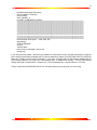
1
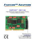
FASTCOM™ ADAPTERS
FASTCOM™: ESCC-PCI
High Speed Dual Channel Sync/Async Interface
for PCI Bus
Hardware Reference Manual
http://www.commtech.com.cn/
COPYRIGHT (C) 1999, 2002, 2003
All rights reserved, including those to reproduce this document or parts thereof in
IBM is a registered trademark of International Business Machines Corporation.
Microsoft is a registered trademark of Microsoft Corporation.
WINDOWS is a trademark of Microsoft Corporation.
REVISION NOTES
REVISION PAGE NUMBER
2.1
27
2.2
8
2.3
26
2.4
26
CHANGES MADE
Changed warranty to 2 years
Added link to installation manual
Updated contact information
Changed warranty period to lifetime
CONTENTS
"CE" CERTIFICATE.............................................................................................................. 1
INTRODUCTION
Description / Block Diagram ............................................................................................ 3
Specifications / Features ................................................................................................. 4
Board Layout ................................................................................................................... 5
DB37 Connector Pin Description ..................................................................................... 6
DB25 Connector Pin Description ..................................................................................... 7
INSTALLATION
Installation ....................................................................................................................... 8
Factory Switch Settings ................................................................................................... 8
Software Installation ........................................................................................................ 8
Testing the Installation
Building the Loopback Plug........................................................................................ 9
Windows NT Test....................................................................................................... 9
Windows 95 Test...................................................................................................... 11
REFERENCE
Switch Descriptions
Clock Control Switch ................................................................................................ 14
485 Control Switch ................................................................................................... 14
Programming ................................................................................................................. 15
RS-422/RS-485 ............................................................................................................. 16
Termination Resistance................................................................................................. 17
PROGRAMMABLE CLOCK GENERATOR (Cypress ICD2053B) ...................................... 18
DETERMINING AND SELECTING BAUD RATES ............................................................. 19
TECHNICAL SUPPORT ..................................................................................................... 26
APPENDIX A
Siemens SAB 82532 Technical Data Sheet .................................................................. 27
1
EUROPEAN UNION DECLARATION OF CONFORMITY
Information Technology Equipment
The Company COMMTECH, INC. declares under its own and full responsibility that the product
" Fastcom: ESCC-PCI - Revision 1.5 "
on which is attached this Certificate is compliant to the "89/336/EEC" Directive, amended by 92/31/EEC and
93/88/EEC.
[ ]
The product identified above complies with the requirements of the above EU Directive by meeting the
following standards:
•
EN 50081-1 (1992) EMC Generic Emission Standard - Part 1, Residential, Commercial and Light Industry
- EN 55022 (1995), CISPR 22 (1993) Limits and Methods of Measurement of Radio Disturbance
Characteristics of Information Technology Equipment, 30 MHz - 1 GHz, Class B Limits
•
EN 50082-1 (1992) EMC Generic Immunity Standard - Part 1, Residential, Commercial and Light Industry
- IEC 801-2 (1984), Method of Evaluating Susceptibility to Electrostatic Discharge, Level 4
- IEC 801-3 (1984), Radiated Electromagnetic field Requirements, Level 3
- IEC 801-4 (1988), Electrical Fast Transient/Burst Requirements, Level 2
Products listed on this declaration are exempt from the requirements of the 73/23/EEC directive due to the input
voltage specification as stated in Article 1 of the directive.
The technical documentation required to demonstrate that this product meets the requirements of the EMC Directive
has been compiled by the signatory below and is available for inspection by the relevant enforcement authorities.
In WICHITA, KS on December 31st of 1995
Mr. Glen R. Alvis
Chief Engineer
2
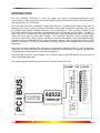
3
INTRODUCTION
The new FASTCOM: ESCC-PCI is a very high speed, dual channel, synchronous/asynchronous serial
communications adapter based upon the Siemens 82532 Enhanced Serial Communication Controller (ESCC),
and is designed for use in the PCI bus.
The FASTCOM: ESCC-PCI is designed to support data rates up to 10 Mbits/second (maximum data rates are
affected by many factors, including computer performance, cable quality, and software overhead), and to reduce
the hardware and software overhead needed for serial communications. Each sync/async channel on the
FASTCOM: ESCC-PCI has its own DPLL encoder/decoder and programmable protocol support. In addition, a
built-in 64 byte FIFO provides the FASTCOM: ESCC-PCI with a very high throughput as well as requiring less
system CPU time than any other HDLC adapter. The FASTCOM: ESCC-PCI directly supports HDLC,
X.25 LAP B, ISDN LAP D, SDLC, ASYNC, and BISYNC protocols, and features a high speed RS-422/RS-485
interface conforming to ANSI/EIA/TIA-530-A-1992 configuration (RS-530). HDLC features include choice of CRC
polynomial (CRC-CCITT or CRC-32), expanded line encoding methods (FM and Manchester), and preamble
transmission.
Many engineers have avoided using synchronous communication adapters because of their programming
complexity. The FASTCOM: ESCC-PCI provides high-speed data communications to designers and engineers,
while greatly reducing development time and system complexity.
The FASTCOM: ESCC-PCI is also available in a PC/104 bus version (FASTCOM: ESCC-104) and an ISA bus
version (FASTCOM: ESCC-ISA).
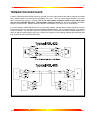
The following diagram illustrates the basic structure of the FASTCOM: ESCC-PCI:
PCI INTERFACE
CONTROLLER
RS-422/485
DRIVERS/RECEIVERS
82532
COMMUNICATION
CONTROLLER
SWITCH 6
RS-485
CONTROL
PCI BUS
CHANNEL 1 (OF 2) RS-530
SD+
SDRD+
RDRTS+
RTSCTS+
CTSDCD+
DCDDSR
DTR
RT+
RT-
4
SPECIFICATIONS:
COMMUNICATION
CONTROLLER:
SIEMENS 82532
DRIVERS/RECEIVERS:
RS-422/RS-485
CONNECTOR CONFIGURATION:
ANSI/EIA/TIA-530-A-1992
POWER REQUIREMENTS:
+5V @ 300mA (TYPICAL)
BUS INTERFACE:
PCI
ENVIRONMENT:
Operating Temperature Range:
Humidity:
0 to 70 C
0 to 90% (non-condensing)
FEATURES:
High speed, up to 10Mbits/s
Much easier to program and use than other HDLC adapters
Supports HDLC, SDLC, ISDN LAP D, and X.25 LAP B, ASYNC, BISYNC
Drivers: RS-422/RS-485 multi-drop
Excellent noise rejection, cable lengths up to 4000 feet
Use low cost "twisted pair" cable
RS-485 mode
Up to 32 FASTCOM: ESCC-PCI adapters can share the same "twisted pair"
Driver control is automatic (via the RTS line)
Serial Interface:
Internal or External Clock Source
Asynchronous, Monosync/Bisync, and HDLC/SDLC data formatting.
1X (isosynchronous) or 16X oversampling for Asynchronous format
Different modes of data encoding (NRZ,NRZI,FM0,FM1,Manchester)
CRC-CCITT or CRC-32 (for HDLC/SDLC modes)
CRC-CCITT or CRC-16 (for BISYNC mode)
Modem control lines (RTS, CTS, DTR, DCD, DSR)
Collision resolution
Programmable bit inversion
Transparent RD/SD of data bytes without HDLC framing
Protocol Support (HDLC/SDLC):
Types of protocol support - Automatic, Manual, Transparent
Handling of bit-oriented functions in all modes
Handling of I and S frames in Auto mode
Modulo 8 and 128 operation
64 byte FIFOs per direction
Storage of up to 17 short received frames
5
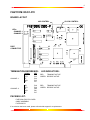
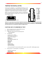
FASTCOM: ESCC-PCI
BOARD LAYOUT
485 CONTROL
LEDs
CHANNEL 1
CHANNEL 2
DB37
CONNECTOR
TERMINATION REFERENCE:
CHANNEL 1:
CHANNEL 2:
SIGNAL
RD
CTS
ST
DCD
RT
REF
R12
R13
R14
R15
R11
RD
CTS
ST
DCD
RT
R18
R19
R20
R21
R17
LED INDICATORS:
RED
GREEN
TRANSMIT ACTIVE
RECEIVE ACTIVE
RED
GREEN
TRANSMIT ACTIVE
RECEIVE ACTIVE
PACKING LIST:
FASTCOM: ESCC-PCI CARD
CABLE ASSEMBLY
FASTCOM CD
If an omission has been made, please call technical support for a replacement.
CLOCK CONTROL
6
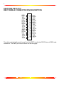
FASTCOM: ESCC-PCI
DB37 FEMALE CONNECTOR PIN DESCRIPTION
GND
2RT+
1RT1DSR
2RD+
2CTS2ST+
2DCD1RD+
1CTS1ST+
1DCD2SD2RTS+
2TT1SD+
1RTS1TT+
1DTR
1
2
3
4
5
6
7
8
9
10
11
12
13
14
15
16
17
18
19
20
21
22
23
24
25
26
27
28
29
30
31
32
33
34
35
36
37
2RT2DSR
1RT+
2RD2CTS+
2ST2DCD+
1RD1CTS+
1ST1DCD+
2SD+
2RTS2TT+
2DTR
1SD1RTS+
1TT-
The cable provided splits each channel from this DB37 to individual RS-530 pin out DB25 male
connectors. The DB25 pin outs are shown on the next page.
7
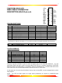
FASTCOM: ESCC-PCI
DB25 CABLE CONNECTOR
DESCRIPTION (RS-530 pin out)
CTS+
STTTDCDRTDCD+
GND
DSR
CTSRTSRDSDGND
PIN DESCRIPTIONS
PIN#
1
7
2
14
3
16
4
19
5
13
DESCRIPTION
SHIELD/GROUND
SIGNAL/GROUND
TRANSMIT DATA
TRANSMIT DATA
RECEIVE DATA
RECEIVE DATA
REQUEST TO SEND
REQUEST TO SEND
CLEAR TO SEND
CLEAR TO SEND
422 TYPE
A
B
A
B
A
B
A
B
CONNECTED TO
GND
GND
SDSD+
RDRD+
RTSRTS+
CTSCTS+
13
12
11
10
9
8
7
6
5
4
3
2
1
25
24
23
22
21
20
19
18
17
16
15
14
TT+
GND
DTR
RTS+
RT+
RD+
ST+
SD+
530 CIRCUIT
AB
BA
BA
BB
BB
CA
CA
CB
CB
The RS-422 "A" side is 0 volts when a "1" is on the line (A side is the negative terminal of the 422 driver).
6
20
DATA SET READY
DATA TERMINAL READY
DSR
DTR
INPUT
OUTPUT
CLOCK SIGNALS
PIN#
8
10
24
11
17
9
15
12
DESCRIPTION
DATA CARRIER DETECT
DATA CARRIER DETECT
TRANSMIT CLOCK OUT
TRANSMIT CLOCK OUT
RECEIVE CLOCK IN
RECEIVE CLOCK IN
TRANSMIT CLOCK IN
TRANSMIT CLOCK IN
422 TYPE
A
B
A
B
A
B
A
B
CONNECTED TO
DCD+
DCDTT+
TTRT+
RTST+
ST-
530 CIRCUIT
CF
CF
DA
DA
DD
DD
DB
DB
These are opposite of RS-422 in order to invert the signals going to the FASTCOM: ESCC-PCI. The 530
specification states that data is valid on the rising edge of the clock (0->1 transition), whereas the FASTCOM:
ESCC-PCI clocks on the falling edge (1->0 transition). DCD is inverted because a "1" at DCD means active to the
FASTCOM: ESCC-PCI, but the 530 specification requires DCD to be "0" to be active.
On the same note, if you are using Clock Mode 1 and you are not using DCD, it must be strapped Active to allow
data reception.
NOTE: The DTR and DSR signals are single ended (unbalanced) as required by ANSI/EIA/TIA-530
specifications.
8
INSTALLATION
Important: Observe Electrostatic Discharge (ESD) precautions when handling the FASTCOM: ESCC-PCI board.
1.
Unpack the FASTCOM: ESCC-PCI. Keep the box and static bag for warranty repair returns.
2.
Check the switches to be sure that they are set as illustrated below (Factory Switch Settings).
3.
Select an open PCI slot in your PC.
4.
After removing the blank bracket from your PC, install the FASTCOM: ESCC-PCI in the PC by pressing it
firmly into the slot. Install the bracket screw to hold it firmly in place.
5.
Re-install the cover on your PC.
FACTORY SWITCH SETTINGS
ON
CLOCK CONTROL (SW5) CLOCK FROM GENERATOR, TXCLK IS OUTPUT
1 2
3 4
5
6 7
8
6 7
8
ON
RS-485 CONTROL (SW6) NO LOOPBACK (422 MODE), CTS DISABLED
1 2
3 4
5
SOFTWARE INSTALLATION
Select the link above to open the Installation Manual. Under Fastcom: ESCC-PCI, select your operating system
and follow the instructions. When you are finished, select Fastcom: ESCC-PCI from the list at the end of the
Fastcom: ESCC-PCI section to return to this manual.
9
TESTING THE INSTALLATION
To fully test the installation of your FASTCOM: ESCC-PCI, you will
need to build a "loop back plug". Materials needed are a DB25 female
receptacle (solder-cup style) and a few short pieces of 20 or 24 AWG
stranded wire. Jumper the pins together on the DB25 as illustrated:
NOTE: You can also create a "loop back" condition on the FASTCOM:
ESCC-PCI without building an adapter plug by setting the 485 Control
Switch (SW6) as follows:
485 CONTROL
ON
1 2
3 4
5
6 7
8
Both ESCC-PCI channels are looped back
1
2
3
4
5
6
7
8
9
10
11
12
13
SIGNALS
14
15
16
17
18
19
20
21
22
23
24
25
2
3
6
7
9
10
11
14
16
17
20
24
SDRDDSR
GND
RTDCDTTSD+
RD+
RT+
DTR
TT+
However, we recommend that you make the "loop back" plug for two reasons: one, the clock circuit can be tested
and, two, you will not have to change switch settings from the factory defaults. In addition, our technical support
engineers can better service your technical questions if you have made the "loop back" plug. If you have made
the loop back plug, do not change the setting of the Mode switch.
FASTCOM: ESCC-PCI WINDOWS NT TEST
1.
2.
3.
4.
Attach a loopback plug to the cable #1 (ESCC0, port 0)
From the Start button menu, select Run
Enter:
D:\fastcom_disks\esccp\nt\escctest\esccptest 0 h
Click the OK button
You should see:
Created esccdrv—ESCC0
ESCC 82532 version status:82
# receive buffers ready:0
resetting
HDLC settings
SETTINGS SUCCESSFUL:168
DTR not SET
DSR not SET
DTR SET
DSR SET
waiting for a key
read thread started
status thread started
(The second DSR SET could be a DSR not SET if you do not have a DTR -> DSR loopback wired)
5.
Press the letter "a" on the keyboard. You should see:
WRITEFILE esccdrv1024
returned TRUE
waiting for a key
10
STATUS, Receive Frame Start
STATUS, All Sent
received 1025 bytes:
aaaaaaaaaaaaa...(12 complete lines and one partial line of "a"s (1024 of them). The last character is not
an "a".)
6.
Press [esc] to exit the program.
You can test channel 1 in a similar manner by running
D:\fastcom_disks\esccp\nt\escctest\esccptest 1 h
Make sure that you move your loopback to cable #2 before running the test on channel 1.
You can test other operating modes by changing the last letter:
Async test:
D:\fastcom_disks\esccp\nt\escctest\esccptest 0 a
HDLC test:
D:\fastcom_disks\esccp\nt\escctest\esccptest 0 h
Bisync test:
D:\fastcom_disks\esccp\nt\escctest\esccptest 0 b
In async you will get a STATUS, Receive Timeout after the All sent message (and possibly at the beginning
before you press a key).
The bisync test will get a STATUS, SYN detected instead of a receive frame start message.
The async test should receive 1024 bytes, displayed as 12.8 lines of the key you pressed.
The HDLC test should receive 1025 bytes, displayed as 12.8 lines of the key you pressed.
The bisync test should receive 1025 bytes, displayed as 12.8 lines of the key you pressed.
The exceptions to this are the keys t, r, i, p and h.
pressing "t" will reset the transmitter and flush the transmit queue
pressing "r" will reset the receiver and flush the receive queue
pressing "i" will start the timer (which will eventually result in a STATUS, Timer expired message. It takes
about a minute in HDLC mode for the timer to timeout)
pressing "p" will stop the timer (which will prevent the STATUS, Timer expired message)
pressing "h" will issue a hunt command in bisync mode
TEST #2
1.
Press the Start Button, select the Run command
Enter: D:\fastcom_disks\esccp\nt\esccpmfc\esccpmfc
Click OK
2.
From the main menu select Options -> Port
Enter 0, click OK
(this selects port 0, make sure you have your loopback on cable #1)
3.
From the main menu select Options -> Settings
(the settings dialog will open)
Click OK
(the TXD status indicator should turn green)
4.
Type a short message on the keyboard, press enter to send it.
The message you typed should appear in the lower window, and the RXD, RFS, and ALLS status indicators
should turn green (if it was a short message (<32 bytes or so); a long message will likely only get an RXD status
indicator).
If when running any of these tests you do not get the expected result, check your loopback plug. Next, check to
11
make sure that the driver loaded and is running ("ESCCPDRV is running" should be displayed in the
NTINSTALL.EXE program window). Watch the BIOS startup screen to verify that the system recognized that the
card is present (installed PCI devices are displayed on some startup sequences). The Fastcom: ESCC-PCI will
be listed as a "Simple Communication Controller". Verify that it is listed, and that the BIOS assigned an IRQ to
the device.
Troubleshooting tips:
1. Incorrect loopback, faulty wiring
2. Board not inserted fully
3. Driver not running/installed
FASTCOM: ESCC-PCI WINDOWS 95 TEST
1.
2.
3.
4.
Install loopback on cable #1 (ESCC0, port0)
From the Start button menu, select Run
Enter:
D:\fastcom_disks\esccp\w95\escctest.exe
Click OK
The display should be:
obtained handle to esccdrv
#ports active:2
Set ICD2053b
ICD2053B set to 16MHz
starting settings......INIT OK
Getting VSTR
VSTR contents:82
WRITE REG (CMDR->XRES)
Write Reg successful
check status
STATUS DECODE:
Transmit Done
flushing rx
RX flushed
flushing tx
TX flushed
read frame
The I/O operation is pending
write frame #1
Write successful
WAIT_OBJECT_0
post GET_OVERLAPPED_RESULT
0123456789012345678901234ó
Read returned :26 bytes — Valid ;CRC..OK ;
STATUS DECODE:
Receive Frame Start
All Sent
Transmit Done
write frame #1
Write #1successful
write frame #2
Write #2 successful
write frame #3 —should pend (no more tbufs)
The I/O operation is pending
12
write frame #4 —should fail (bufs full)
Tx buffers full; try again later.
read frame (should get 4001 bytes)
The I/O operation is pending
Read Timeout
Read Timeout
WAIT_OBJECT_0
post GET_OVERLAPPED_RESULT
01234567890123456789012345678901234567890123456789012345678901234567890123456789012345678901234567890123456789012345678901234
56789012345678901234567890123456789012345678901234567890123456789012345678901234567890123456789012345678901234567890123456789
01234567890123456789012345678901234567890123456789012345678901234567890123456789012345678901234567890123456789012345678901234
56789012345678901234567890123456789012345678901234567890123456789012345678901234567890123456789012345678901234567890123456789
01234567890123456789012345678901234567890123456789012345678901234567890123456789012345678901234567890123456789012345678901234
56789012345678901234567890123456789012345678901234567890123456789012345678901234567890123456789012345678901234567890123456789
01234567890123456789012345678901234567890123456789012345678901234567890123456789012345678901234567890123456789012345678901234
56789012345678901234567890123456789012345678901234567890123456789012345678901234567890123456789012345678901234567890123456789
01234567890123456789012345678901234567890123456789012345678901234567890123456789012345678901234567890123456789012345678901234
56789012345678901234567890123456789012345678901234567890123456789012345678901234567890123456789012345678901234567890123456789
01234567890123456789012345678901234567890123456789012345678901234567890123456789012345678901234567890123456789012345678901234
56789012345678901234567890123456789012345678901234567890123456789012345678901234567890123456789012345678901234567890123456789
01234567890123456789012345678901234567890123456789012345678901234567890123456789012345678901234567890123456789012345678901234
56789012345678901234567890123456789012345678901234567890123456789012345678901234567890123456789012345678901234567890123456789
01234567890123456789012345678901234567890123456789012345678901234567890123456789012345678901234567890123456789012345678901234
56789012345678901234567890123456789012345678901234567890123456789012345678901234567890123456789012345678901234567890123456789
01234567890123456789012345678901234567890123456789012345678901234567890123456789012345678901234567890123456789012345678901234
56789012345678901234567890123456789012345678901234567890123456789012345678901234567890123456789012345678901234567890123456789
01234567890123456789012345678901234567890123456789012345678901234567890123456789012345678901234567890123456789012345678901234
56789012345678901234567890123456789012345678901234567890123456789012345678901234567890123456789012345678901234567890123456789
01234567890123456789012345678901234567890123456789012345678901234567890123456789012345678901234567890123456789012345678901234
56789012345678901234567890123456789012345678901234567890123456789012345678901234567890123456789012345678901234567890123456789
01234567890123456789012345678901234567890123456789012345678901234567890123456789012345678901234567890123456789012345678901234
56789012345678901234567890123456789012345678901234567890123456789012345678901234567890123456789012345678901234567890123456789
01234567890123456789012345678901234567890123456789012345678901234567890123456789012345678901234567890123456789012345678901234
56789012345678901234567890123456789012345678901234567890123456789012345678901234567890123456789012345678901234567890123456789
01234567890123456789012345678901234567890123456789012345678901234567890123456789012345678901234567890123456789012345678901234
56789012345678901234567890123456789012345678901234567890123456789012345678901234567890123456789012345678901234567890123456789
01234567890123456789012345678901234567890123456789012345678901234567890123456789012345678901234567890123456789012345678901234
56789012345678901234567890123456789012345678901234567890123456789012345678901234567890123456789012345678901234567890123456789
01234567890123456789012345678901234567890123456789012345678901234567890123456789012345678901234567890123456789012345678901234
56789012345678901234567890123456789012345678901234567890123456789012345678901234567890123456789012345678901234567890123456789ó
Read returned :4001 bytes — Valid ;CRC..OK ;
check status
STATUS DECODE:
Receive Frame Start
read frame(should get 3001 bytes)
The I/O operation is pending
Read Timeout
WAIT_OBJECT_0
post GET_OVERLAPPED_RESULT
01234567890123456789012345678901234567890123456789012345678901234567890123456789012345678901234567890123456789012345678901234
56789012345678901234567890123456789012345678901234567890123456789012345678901234567890123456789012345678901234567890123456789
01234567890123456789012345678901234567890123456789012345678901234567890123456789012345678901234567890123456789012345678901234
56789012345678901234567890123456789012345678901234567890123456789012345678901234567890123456789012345678901234567890123456789
01234567890123456789012345678901234567890123456789012345678901234567890123456789012345678901234567890123456789012345678901234
56789012345678901234567890123456789012345678901234567890123456789012345678901234567890123456789012345678901234567890123456789
01234567890123456789012345678901234567890123456789012345678901234567890123456789012345678901234567890123456789012345678901234
56789012345678901234567890123456789012345678901234567890123456789012345678901234567890123456789012345678901234567890123456789
01234567890123456789012345678901234567890123456789012345678901234567890123456789012345678901234567890123456789012345678901234
56789012345678901234567890123456789012345678901234567890123456789012345678901234567890123456789012345678901234567890123456789
01234567890123456789012345678901234567890123456789012345678901234567890123456789012345678901234567890123456789012345678901234
56789012345678901234567890123456789012345678901234567890123456789012345678901234567890123456789012345678901234567890123456789
01234567890123456789012345678901234567890123456789012345678901234567890123456789012345678901234567890123456789012345678901234
56789012345678901234567890123456789012345678901234567890123456789012345678901234567890123456789012345678901234567890123456789
01234567890123456789012345678901234567890123456789012345678901234567890123456789012345678901234567890123456789012345678901234
56789012345678901234567890123456789012345678901234567890123456789012345678901234567890123456789012345678901234567890123456789
01234567890123456789012345678901234567890123456789012345678901234567890123456789012345678901234567890123456789012345678901234
56789012345678901234567890123456789012345678901234567890123456789012345678901234567890123456789012345678901234567890123456789
01234567890123456789012345678901234567890123456789012345678901234567890123456789012345678901234567890123456789012345678901234
56789012345678901234567890123456789012345678901234567890123456789012345678901234567890123456789012345678901234567890123456789
01234567890123456789012345678901234567890123456789012345678901234567890123456789012345678901234567890123456789012345678901234
56789012345678901234567890123456789012345678901234567890123456789012345678901234567890123456789012345678901234567890123456789
01234567890123456789012345678901234567890123456789012345678901234567890123456789012345678901234567890123456789012345678901234
56789012345678901234567890123456789012345678901234567890123456789012345678901234567890123456789012345678901234567890123456789á
Read returned :3001 bytes — Valid ;CRC..OK ;
check status
STATUS DECODE:
Receive Frame Start
Transmit Done
13
read frame(should get 2001 bytes)
The I/O operation is pending
Read Timeout
WAIT_OBJECT_0
post GET_OVERLAPPED_RESULT
01234567890123456789012345678901234567890123456789012345678901234567890123456789012345678901234567890123456789012345678901234
56789012345678901234567890123456789012345678901234567890123456789012345678901234567890123456789012345678901234567890123456789
01234567890123456789012345678901234567890123456789012345678901234567890123456789012345678901234567890123456789012345678901234
56789012345678901234567890123456789012345678901234567890123456789012345678901234567890123456789012345678901234567890123456789
01234567890123456789012345678901234567890123456789012345678901234567890123456789012345678901234567890123456789012345678901234
56789012345678901234567890123456789012345678901234567890123456789012345678901234567890123456789012345678901234567890123456789
01234567890123456789012345678901234567890123456789012345678901234567890123456789012345678901234567890123456789012345678901234
56789012345678901234567890123456789012345678901234567890123456789012345678901234567890123456789012345678901234567890123456789
01234567890123456789012345678901234567890123456789012345678901234567890123456789012345678901234567890123456789012345678901234
56789012345678901234567890123456789012345678901234567890123456789012345678901234567890123456789012345678901234567890123456789
01234567890123456789012345678901234567890123456789012345678901234567890123456789012345678901234567890123456789012345678901234
56789012345678901234567890123456789012345678901234567890123456789012345678901234567890123456789012345678901234567890123456789
01234567890123456789012345678901234567890123456789012345678901234567890123456789012345678901234567890123456789012345678901234
56789012345678901234567890123456789012345678901234567890123456789012345678901234567890123456789012345678901234567890123456789
01234567890123456789012345678901234567890123456789012345678901234567890123456789012345678901234567890123456789012345678901234
56789012345678901234567890123456789012345678901234567890123456789012345678901234567890123456789012345678901234567890123456789ó
Read returned :2001 bytes — Valid ;CRC..OK ;
check status
STATUS DECODE:
All Sent
Transmit Done
Press a key to send again, [esc] to exit
exiting prog
If you don't get these results, verify that your loopback is constructed correctly, and that the board is recognized
by the system (some BIOS will display the PCI devices installed on startup; the FASTCOM: ESCC-PCI should be
listed as a "Simple Communications Controller"). If you have a system with PCI IRQ steering enabled and are
encountering problems, you might try the Windows98 driver, or disable IRQ steering. The PCI IRQ steering
settings are found in Control Panel -> System Icon -> Device Manager tab -> System Devices -> PCI Bus.
Finally, verify that the ESCCPDRV.VXD file is in the same directory as the program you are running.
14
SWITCH DESCRIPTIONS
There are two dip switches on the FASTCOM: ESCC-PCI, labeled SW5, and SW6 (See Board Layout Illustration
for location). Switch 5 (CLOCK CONTROL) selects the input to the oscillator pin of the ESCC chip and controls
the direction of the transmit clock signals (input or output). Switch 6 (485 CONTROL) selects either RS-422 or
RS-485 mode.
SWITCH 5, CLOCK CONTROL
POSITION
1
2
3
4
5
6
7
8
DESCRIPTION
Selects the output of the clock generator (ICD2053B) as the input to OSC on the ESCC.
Selects the output of the CLOCK (18.432 MHz) as the input to OSC on the ESCC.
Not used.
Not used.
Connects the TXCLK pin of the ESCC channel 0 to the output driver (TT is TXCLK).
Makes TXCLK an output.
Connects the TXCLK pin of the ESCC channel 0 to the input receiver (ST is TXCLK).
Makes TXCLK an input.
Connects the TXCLK pin of the ESCC channel 1 to the output driver (TT is TXCLK).
Makes TXCLK an output.
Connects the TXCLK pin of the ESCC channel 1 to the input receiver (ST is TXCLK).
Makes TXCLK an input.
The TXCLK input/output switch connects the TXCLK pin on the 82532 to either the TT signal lines (to output the
transmit timing), or the ST signal lines (to input the transmit timing). If the input selection is made with position 6
or 8 on, do not configure the 82532 TXCLK pin as an output!
SWITCH 6, 485 CONTROL
POSITION
1
2
3
4
5
6
7
8
DESCRIPTION
TXD+ to RXD+ loopback for RS-485 channel 0
TXD- to RXD- loopback for RS-485 channel 0
TXD+ to RXD+ loopback for RS-485 channel 1
TXD- to RXD- loopback for RS-485 channel 1
CTS disable for channel 0 (CTS is forced true if switch is on; CTS comes from connector if off)
CTS disable for channel 1 (CTS is forced true if switch is on; CTS comes from connector if off)
RS-485 driver control enable for channel 0 (in on position, RTS controls the TXD driver enable)
RS-485 driver control enable for channel 1 (in on position, RTS controls the TXD driver enable)
The 485 Control switch controls the RS-485 loopback feature, connecting the SD+/- signals to the RD+/- signals
internally so you don't have to make the connection on your cable. It also controls the CTS disable feature. Since
the 82532 will only transmit when its CTS pin is active, this switch allows the 82532 to see the CTS input as active
all the time, regardless of the signal at the connector.
The loopback switch positions are provided for RS-485 mode and should be used in pairs. Positions 1 and 2
should either be on, creating a loopback for RS-485 mode, or off, for RS-422 mode. Likewise, positions 3 and 4
should either both be on or both off.
The CTS disable switch is used to force CTS into the active state (in the on position) to allow the 82532 to
transmit data if the CTS signal line is not used. In the off position, the CTS signal from the connector is
connected to the 82532, and the 82532 will not transmit unless the external CTS signal is active!
15
PROGRAMMING
Refer to the enclosed FASTCOM CD for example programs, product updates, and software for testing your
installation. Refer to the Siemens SAB 82532 User's Manual for register information.
NOTES
Always set the SAB 82532 port configuration register (PCR) to E0H.
Always set the SAB 82532 interrupt port configuration (IPC) to 03H.
Always set the SAB 82532 CCR1 ODS bit to 1.
The PCI controller chip (AMCC S5933Q) is used in "pass-through" mode to connect to the ESCC chip
(SAB 82532). The interrupt line is connected from the 82532 to mailbox 4, byte 3.
Examples for programming the interrupt configuration and for servicing interrupts can be found in the
CESCCP.CPP class library file.
SAB 82532 PVR Register
The 82532 has an 8 bit I/O port (PVR) that has the following functions on the FASTCOM: ESCC-PCI.
Bit::
0 - Clock generator data
1 - Clock generator clock
2 - N/C
3 - DTR channel 1 (output)
4 - DTR channel 2 (output)
5 - DSR channel 1 (input)
6 - DSR channel 2 (input)
7 - N/C
16
RS-422 / RS-485
Most engineers have worked with RS-232 devices at least once in their career. If you have never worked with
RS-422 or RS-485 devices, you will be pleased to know that working with the FASTCOM: ESCC-PCI is not much
different from working with an RS-232 device.
The RS-422 standard was developed to correct some of the deficiencies of RS-232. In commercial and industrial
applications, RS-232 has some significant problems. First, the cable length between RS-232 devices must be
short (usually less than 50 feet at 9600 Baud). Second, many RS-232 errors are the result of cables picking up
normal industrial electrical noises such as fluorescent lights, motors, transformers, and other EMF sources. Third,
RS-232 data rates are functionally limited to 19.2K Baud. On the other hand, the newer RS-422 standard makes
cable lengths up to 5000 feet possible and is highly immune to most industrial noises. Data rates are also
improved -- the FASTCOM: ESCC-PCI features data rates up to 10 Mega Baud. These improvements were
made possible by differentially driving and receiving the data as opposed to the single ended method employed
by the RS-232 standard. With the RS-422 standard, the transmit signal (TX in RS-232) is a differential signal
consisting of SD+ and SD-; the receive signal (RX in RS-232) consists of RD+ and RD-.
Another draw back of RS-232 is that more than two devices cannot share a single cable. This is also true of
RS-422, and that's why the RS-485 standard was developed. RS-485 offers all of the benefits of RS-422 and
also allows multiple units (up to 32) to share the same twisted pair. RS-485 is often referred to as a "multi-drop"
or "two-wire, half duplex" network because the drivers (transmitters) and receivers share the same two lines. In
fact, up to 32 stations can share the same "twisted pair". In order for an RS-485 system to work, only one driver
(transmitter) can occupy the network at a time. This means that each station on the network must control the
enabling/disabling of their drivers in order to avoid network conflicts. If two drivers engage the network at the
same time, data from both will be corrupted. In RS-485 mode, the receivers are always enabled.
For a more detailed description of RS-422 and RS-485, we recommend the following references:
LINEAR AND INTERFACE CIRCUITS APPLICATIONS, Volume 2: Line Circuits, Display Drivers. By
D.E. Pippenger and E. J. Tobaben. Published 1985 by Texas Instruments. ISBN-0-89512-185-9
Note: This book may be difficult to find in a bookstore. The best place to get it is directly from Texas
Instruments or from one their component dealers. Publication # SLYA002.
"Driver/Receiver Family Extends Data-Link Performance", ELECTRONIC PRODUCTS, January 15, 1985.
By Dale Pippenger and Joe Miller
17
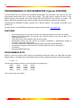
TERMINATION RESISTANCE
In both the RS-422 and the RS-485 mode, the receiver end of the cable between two stations must be terminated
with a resistor equal to the characteristic impedance of the wire. This is to prevent signal reflections in the wire
and to improve noise rejection. However, you do not need to add a terminator resistor to your cables when
you use the FASTCOM: ESCC-PCI. The termination resistance is built in. We have installed a terminator
resistor for each receiver: between each RD+ and RD- and between CTS+ and CTS- for each channel.
If you are using the FASTCOM: ESCC-PCI in a multi-drop network, the termination resistor should be removed
from all units except the first and last (see the RS-485 illustration below). Call for technical support if you need to
modify the resistor. You may also order the FASTCOM: ESCC-PCI without the termination resistor installed (it is
easier to add the resistor than to remove it). Observe the resistors in the following drawings and remember that
they are built into the FASTCOM: ESCC-PCI:
18
PROGRAMMABLE CLOCK GENERATOR (Cypress ICD2053B)
The FASTCOM: ESCC-PCI features the ICD2053B Programmable Clock Generator, which offers a fully userprogrammable phase-locked loop in a single 8-pin package. The output may be changed "on the fly" to any
desired frequency value between 391 kHz and 90 MHz (the FASTCOM: ESCC-PCI maximum is 33 MHz). The
ability to dynamically change the output frequency adds a whole new degree of freedom for the designer.
Programming the ICD2053B is simple, requiring only a "bitcalc" program. This program is provided on the
Fastcom CD.
The data sheet for the ICD2053B also explains the operation of this program. Open data sheet
FEATURES
•
•
•
•
•
•
•
•
Clock outputs ranging from 391 kHz to 90 MHz (the FASTCOM: ESCC-PCI maximum is 33 MHz)
Phase-Locked Loop oscillator input derived from external reference clock (18.432 MHz on the
FASTCOM: ESCC-PCI)
Three-State output control disables output for test purposes
Sophisticated internal loop filter requires no external components or manufacturing tweaks as
commonly required with external filters
Low power consumption makes device ideal for power- and space-critical applications
Programmable using the FASTCOM: ESCC-PCI PVR register, bits 0 and 1 (see page 17)
5V operation
High-speed CMOS technology
PROGRAMMING NOTE
Revision 3.2A of the Siemens 82532 utilizes both standard and enhanced modes of the Baud Rate Generator
Register (BGR). In standard mode, the following formula is used to calculate the divisor for baud rate generation:
k = (N+1) * 2
The following hexadecimal values of N are equivalent to N equaling zero:
0x000
0x100
0x200
0x300
0x040
0x140
0x240
0x340
0x080
0x180
0x280
0x380
0x0C0
0x1C0
0x2C0
0x3C0
This is a known bug of the 82532.
19
DETERMINING AND SELECTING BAUD RATES
Selecting the bit rate can either be very easy or quite complicated, depending on a number of factors. The best
place to start is to determine the big picture (broad perspective) and narrow down the options using the various
constraints that the hardware imposes.
There are four basic things that make up what the actual bitrate will be. They are:
1. Register settings of the 82532 chip. These include:
A. Operating mode (HDLC, Bisync, Async)
1. If async is used is it truly async (oversampled BCR=1), or
2. isosynchronous (async format with no oversampling).
B. Clock mode (internal or external clocks)
1. If internal clocks, does it use clock recovery (DPLL)
2. If BGR is used is the BDF bit 1 or 0.
2. The setting of the clock generator (ICD2053B) that feeds the OSC input to the 82532 (only a factor if
an internal clock mode is used, i.e., BGR or DPLL is involved).
3. The physical switch settings of the Fastcom: ESCC-PCI.
A. The switch determines the routing of the TXCLK pin as either an input or output.
B. The switch also determines if the OSC is fed the output of the clock generator or just the output of
the onboard clock (an option on the ESCC-PCI and the HSCX; the ESCC-ISA does not have this
option).
4. The revision of the ESCC 82532 chip (silicon)
A. The rev 3.2 silicon incorporates an enhanced baud rate mode.
We will start with the simplest case. If you are using the Asynchronous data mode, then the most likely clock
mode that you should use is 7b. It is possible to use the other clock modes; however, mode 7b is the most
straightforward to work with. The bitrate will be determined by the output of the baud rate generator. The baud
rate generator is clocked by the OSC input (which is set by the ICD2053B clock generator). So you have:
If you are not using oversampling (BCR = 0) the formula is:
bitrate = (input clock / BGR)
If you are using oversampling (BCR = 1 (the normal case for async)) the formula is:
bitrate = (input clock / BGR)/16
If BDF = 1
If BDF = 0
If BDF = 0 and EBRG = 1
then BGR = 1
then BGR = (N+1)*2
then BGR = (n+1)*2m
The BCR bit is in CCR1 (bit 3)
The BDF bit is in CCR2 (bit 5)
The EGRG bit is in CCR4 (bit 6)
N = (CCR2&0xC0)<<2) + BGR, or if you prefer
n=
m=
N=
Most significant bit________________________Least significant bit
BGR bit 5, BGR bit 4, BGR bit 3, BGR bit 2, BGR bit 1, BGR bit 0
CCR2 8, CCR2 7, BGR 7, BGR 6
CCR2 8, CCR2 7, BGR 7, BGR 6, BGR 5, BGR 4, BGR 3, BGR 2, BGR 1, BGR 0
Some things to keep in mind:
The range on the ICD2053B output is 391kHz to 90MHz.
The usable range if the master clock enable bit is clear (not using master clock) is 391kHz to 33Mhz. If
the master clock is set, then the range is from 391kHz to 10MHz.
Using master clock mode also places a restriction on the ratio of receive/transmit clock to the master
clock frequency (as per note 2 on page 84 of the 82532 data sheet).
20
Fmaster/Ftransmit >= 2.5
Freceive/Fmaster <3 or 1.5 (if CCR3 bit 4 (RADD) is set and an address recognition mode is used in
HDLC).
To use Master clock mode or not to use Master clock mode; that is the question.
The 82532 operating in standard (non-master clock) mode uses the transmit clock source (refer to table 5 page
84 of the data sheet) to run the internal timing of the chip. If your transmit clock source is running very slow or it is
not running continuously (if external clock is supplied), then it is a good idea to switch to master clock mode.
Each command issued to the 82532 (any write to the CMDR register) can take up to 2.5 clocks to complete. If the
clock is very slow or stops from time to time, this can be a significant amount of time and allows for the possibility
of a command being lost (written but not executed, because a previous command is not complete). If your baud
rate is slow (<1MHz) or you are using a gated external clock, you should use master clock mode to allow the PC
interface to the 82532 to continue to execute quickly. If this mode is used, then the OSC input must be less than
10MHz (the speed rating of the internals of the 82532). If you have a 82532 rev 3.x (silicon), then you can cause
the master clock to be OSC/4 by setting CCR4 bit 7 (MCK4), thus allowing the 10MHz restriction to be lifted.
If you are using a clock mode that uses external clocks, you should respect the restriction on the ratio of receive
to transmit clock frequency given in note 2 of table 5 (Freceive/Ftransmit <3 or 1.5).
If you are running in not extended baud rate mode, do not set BGR bits 5-0 to all = 0, or the chip will assume that
all of the BGR bits are 0. This is a glitch in the 82532 rev 3.2 and makes the following values for N identical:
0x000,0x040,0x080,0x0C0
0x100,0x140,0x180,0x1C0
0x200,0x240,0x280,0x2C0
0x300,0x340,0x380,0x3C0
Setting the baud rate generator to any of these values will produce the same affect as setting it to 0x000.
If you use the Enhanced baud rate generator and set m = 0, the clock output will be asymmetric (non 50/50 duty
cycle).
To determine the parameters that need to be sent to the ICD2053B part, you will need to obtain the bitcalc3
program from Cypress. It can be found on the web at:
http://www.cypress.com/cypress/tech_sup/web_tech/sw/clocks.html
After you have downloaded and installed it select:
Devices->programmable products->ICD2053B->CLKOUT from the menu.
Type in 18.432 MHz for the reference frequency (for the ESCC-ISA and ESCC-PCI, for the HSCX type in 16.000
MHz). Enter the desired frequency (keeping in mind all of the restrictions noted above), and press the calculate
button. Write down the Hex programming word (stuffed) and count the number of bits in the binary word. These
are the parameters that need to be passed to the IOCTL_ESCCDRV_SET_CLOCK function to program the
ICD2053B to get the desired frequency output.
An important fact about the clock generator
There is only one ICD2053B part, and only 1 OSC input to the 82532 chip. The clock generator can be
programmed from either channel (ESCC0 or ESCC1), but it programs the same part. The result is that while the
baud rate generators are unique on a per channel basis, the OSC input is not (i.e., the baud rate generators are
independent, but the clock that feeds them is the same). If you change the clock generator output you will change
the input clock to both channels. The practical thing to note about this is that if you have multiple baud rates that
must be generated on multiple channels, you should select the input clock (ICD 2053B output) such that all baud
rates can be derived from one clock value. Changing the clock generator output will affect the baud rates of both
channels (ESCC0, ESCC1)!!!!
21
If you are using HDLC or Bisync as a data format, there is not a BCR setting (no oversampling). However, if you
select a clock mode that uses the DPLL as a source, it will effectively add a divide by 16 to your function.
Selecting the appropriate clock mode is a matter of identifying what clock signals are available external to the
Fastcom card, and what clock signals are required by the external device. The simplest mode is using external
clocks only (mode 0a); in this mode both the receive and transmit timing are taken from the connector (RT for
receive, ST for transmit). The rest of the modes are a mix of external signals and internally generated
clocks/clock recovery. The DPLL modes only operate up to 2 MHz. If the bitrate is above that, you should use a
non-DPLL mode.
The bitrate functions are similar to the async case:
If you are not using a clock mode that uses the DPLL, the formula is:
bitrate = (input clock / BGR)
If you are using the DPLL, the formula is:
bitrate = (input clock / BGR)/16
The input clock will depend on the clock mode. It is usually either the OSC input or the RXCLK (RT+/-) input (see
table 5 page 84 of the 82532 data sheet).
If BDF = 1
If BDF = 0
If BDF = 0 and EBRG = 1
BGR = 1
BGR = (N+1)*2
BGR = (n+1)*2^m (V 3.x of the 82532 silicon only)
The BDF bit is in CCR2 (bit 5)
N = (CCR2&0xC0)<<2) + BGR, or if you prefer
m=
n=
N=
Most significant
Least significant bit
CCR2 bit 8,CCR2 bit 7, BGR bit 7, BGR bit 6
BGR 5, BGR 4, BGR 3, BGR 2, BGR 1, BGR 0
CCR2 8,CCR2 7, BGR 7, BGR 6, BGR 5, BGR 4, BGR 3, BGR 2, BGR 1, BGR 0
If you are using the DPLL, you should try to set its input clock to be as close to the actual bit frequency as
possible. This will allow for optimal clock recovery. Also, clock recovery relies on edges in the data stream; if you
transmit long segments of 0s or 1s using an encoding method that produces no edges, the results will be nonoptimal. The ideal encoding for clock recovery is Manchester or a non ‘1’ idle pattern (i.e., constant flag
sequences on idle if HDLC is used, etc.).
Let’s start with something easy
Let’s say that you want to set up an ESCC channel to run in HDLC mode at 19200 bps, that the device in
question supplies a clock with its data (receive clock), and that we need to generate (transmit) a clock that
matches our transmitted data. To achieve this we should set the 82532 to clock mode 0b. Set the mode switch
position 5 (or 7) to on, enabling the txclk output driver (selecting txclk as an output on TT+/-). The baudrate
function bitrate = input clock / (N+1)*2 will be used. If there are no other constraints other than operating one
channel at 19200 bps, then we can select both the input clock and N arbitrarily, so long as we do not violate any
of the notes.
So, by selecting a value for input clock that is less than 10 MHz (since the bit rate is slow we will want to use
master clock mode, which will require a 10 MHz or less clock), we can then calculate the value needed for N to
get a 19200 bps output. I will pick 7.372800 MHz for the input clock. To get the programming word for this
frequency, I run bitcalc and enter the reference frequency (18.432 MHz) and the desired frequency, and get the
following values:
clkbits = 0x0E9920 (the stuffed (hex) programming word), and
22
numbits = 23 (the number of bits in the stuffed programming word (counted from the stuffed binary word)).
Calling the IOCTL_ESCCDRV_SET_CLOCK ioctl function with these parameters will get us an input clock of
7.3728 MHz (referred to as OSC in table 5).
Then solving for N we get:
19200 = 7.3728E6/((N+1)*2)
N = 191 = 0x0BF
Checking the notes to make sure we did not violate anything:
Fm/Fx = 7.3728E6/19200 = 384 > 2.5 (we are OK on this one)
Fr/Fm = rxclk input / 7.3728E6 < 3 (assuming a 19200 clock input) 19200/7.3728E6 = .0026 < 3 (we are
OK on this one)
(0x0BF & 0x3f) <= 0 (checking the value of n to make sure it isn’t forced to zero due to the glitch in the
82532)
Important Register Settings
MODE = 0x88
This sets the 82532 in transparent HDLC mode 0. This will use a frame structure as:
0x7E | data | CRC | CRC | 0x7E
No address recognition is used
The timer is in external mode
RTS is handled by the 82532 (active while transmitting)
Timer resolution is 32768 clocks
CCR0 = 0xC0
This sets the 82532 in power up mode
Master clock mode is enabled
NRZ is the encoding type
HDLC mode is selected
CCR1 = 0x10
This selects clock mode 0(b)
The tx pin is using a push-pull output (required)
Time fill is all ‘1’s (idle pattern = 0xff)
CCR2 = 0x38
This selects the BGR = (N+1)*2 divisor
Selects txclk to be an output
Selects clock mode 0b (the B part)
Enables the CRC-CCITT polynomial
CCR3 = 0x00
No preamble output
CRC reset level = 0xffff
CRC is in use (both transmit and receive), not including CRC in received Data (not returned to the
user)
Not using extended window for DPLL
CCR4 = 0x00
Not using master clock/4
Not using enhanced baud rate generator
FIFO threshold is 32 bytes (mandatory for NT driver in HDLC mode)
BGR = 0xBF
This sets the output clock rate to 19200 (given that the input clock was previously set to 7.3728
23
MHz, and the above registers are set as shown)
CCR0, CCR1, CCR4 and BGR are the most critical registers that effect the bitrate, the rest are shown for
completeness, and, depending on the system, you can easily change some parameters without affecting the
bitrate (i.e., line encoding, address recognition, crc type, etc.).
And now for something a bit more difficult:
Let’s say that you want to run one channel asynchronously at 38400 bps, and the second channel synchronously
using HDLC at 2 Mbps. How would you go about it?
Start with the fastest bit rate and determine if there is an external clock that is received with that data or if the
clock must be recovered (DPLL mode). Let’s say that you want to recover the clock from the data (there are no
clock lines in the system), and that the data is Manchester encoded. To get a 2 Mbps clock rate using a DPLL we
will need to use the bitrate = (input clock/1)/16 function. This will require a 32 MHz input clock. To get this input
clock using bitcalc as before:
clkbits = 0x5D0C60
numbits = 23
using the following register settings:
MODE = 0x88
CCR0 = 0x98
CCR1 = 0x16
CCR2 = 0x18
CCR3 = 0x00
CCR4 = 0x00
The receive source will be recovered from the data stream. The transmit source will be the BGR/16 output.
Now for the async channel. We are locked into the 32 MHz input clock, so we will try to find a value for N that
gets our desired 38400 bps:
38400 = (32E6/16)/((N+1)*2)
N = 25.04 (we cannot attain non-integer values for N).
If we use N = 25 we would get:
bitrate = (32E6/16)/(25+1)*2 = 38462 bps
If we use N = 26 we would get:
bitrate = (32E6/16)/(26+1)*2 = 37037 bps
Using the closest value and setting the registers to
MODE = 0x08,
CCR0 = 0xC3,
CCR1 = 0x1F,
CCR2 = 0x38,
CCR3 = 0x00,
CCR4 = 0x80, and
BGR = 0x19
will yield an asynchronous data format (with 16X oversampling) at about 38400 bps.
If later you decide that you need to get 115200 bps on the async channel you will find:
115200 = (32E6/16)/((N+1)*2)
N = 7.68
Using N = 7
bitrate = (32E6/16)/((7+1)*2) = 125000 bps
24
Using N = 8
bitrate = (32E6/16)/((8+1)*2) = 111111 bps
The ideal situation would be to adjust the 32 MHz clock such that the deviation between the desired and actual
rates is spread between both channels (with the DPLL recovering the clock, the actual clock that feeds it is not as
critical as a clock mode that uses the clock directly).
Clock modes 0b, 3b, 4, and 7b are more sensitive to the selected rate in synchronous modes, as there is no
oversampling. The rate you select is the rate you will get, whereas oversampling modes (using the DPLL or
ASYNC BCR) are more tolerant to differences between the rate you set and the rate you want.
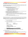
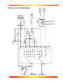
RT+
RT-
TT+
TT-
Clocking Concept Block Diagram
ST+
ST-
25
Channel 1
Switch positions 5 & 6
Channel 2
Switch positions 7 & 8
TxCLK
RxD
RxCLK
Clock
Generator
(ICD2053B)
Oscillator
2a/b
3a/b
0b
6a/b
7a/b
4:1
BRG
16:1
0a
2a
6a
f TRM
4
2a/b 3b
3a 7b
6a/b
7a
0a/b
1
5
f REC
CCR0
MCE=1
0
Core
Transmitter
f TxCLK
f RxCLK
1
5
f BRG
2b
6b
f RxCLK
f DPLL
0b
3b
7b
f TxCLK
3a
7a
f BRG/16
f RxCLK
4
f BRG
f BRG/16
f BRG
f DPLL
f DPLL
f OSC
f OSC
DPLL
f OSC
CCR4
MCK=0
1
Receiver
26
TECHNICAL SUPPORT
All products manufactured by Commtech are warranted against defective materials and workmanship for the
lifetime of the product. This warranty is available only to the original purchaser. Any product found to be
defective will, at the option of Commtech, be repaired or replaced with no charge for labor or parts not excluded
by the warranty. This warranty does not apply to any products that have been subjected to misuse, abuse, or
accident or as a result of service or modification by anyone other than Commtech. In no case shall Commtech
liability exceed the original product purchase price.
If any Commtech product is damaged such that it cannot be repaired, you can return it to Commtech for
replacement under our Non-Repairable Replacement policy, regardless of the cause of damage. Commtech will
replace the unit at 60% of the then-current list price.
Commtech provides extensive technical support and application suggestions. Most of the problems that occur
with the FASTCOM: ESCC-PCI can be corrected by double-checking the switch positions, your cables and your
program. We recommend that you build the loop back plug that is described in the Programming section of this
manual. With that plug, you can quickly isolate the problem to the board, cables, or software.
If you still have unresolved questions, use the following procedure to get technical support:
1.
Call our Technical Support Staff . They are on duty from 9:00 AM to 5:00 PM Central
2.
Ask for technical support for the FASTCOM: ESCC-PCI. Be ready to describe the problem, your computer
system, your application, and your software.
3.
If necessary, our staff will give you an RMA number (Return Material Authorization). Use this number on
the mailing label and in all references to your board. Put the board back in its static bag and in its box.
Ship the board back to us as directed.
27
APPENDIX A
SAB 82532
TECHNICAL DATA