1
®
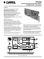
PC-420
FUNCTIONAL SPECIFICATIONS
(Typical at +25°C, dynamic conditions, unless noted)
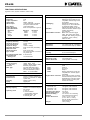
WAVEFORM OUTPUTS
Number of Channels
Amplitude
Output Impedance
Update Rate
Offset Adjust
Gain Adjust
Output Protection
Output Bandwidth
Waveform
Sine
Square
Ramp
Triangle
PC/AT BUS INTERFACE
2, non-isolated
±10V
50Ω
40MHz, maximum
12-bit unipolar DAC, adjustable
from plus to minus full scale
12-bit unipolar DAC
Short circuit protection to ground
Architecture
I/O Mapping
Data Bus
Max Freq.
10MHz
10MHz
100kHz
100kHz
Resolution
0.012%
0.012%
0.012%
0.012%
Control/Status Function
OUTPUT PERFORMANCE
Frequency Range
Frequency Accuracy
Amplitude Accuracy
Loop Lock Up Time
Amplitude Range
Amplitude Resolution
Maximum Offset
Offset Resolution
Sync. Output
TTL Output Rise/Fall Time
Gain/Offset DAC
Settling Time
2.3 x 10⁻³ Hz to 10MHz
±0.012%
±0.25% of FSR
250ms
+10mV to +20Vpp
0.05% of full scale (12-bit DAC)
±10V
0.05% of full scale
TTL levels into 50W, on channel 0
only, active high
5 nanoseconds
SQUARE WAVE
15 microseconds
Sample Rate
Waveform Length
Vertical Resolution
Rise/Fall Time
Asymmetry
Overshoot
Rise/Fall Time
Linearity
Accuracy
Aging
7 selectable, 1 fixed (20MHz)
10MHz, 5MHz, 1MHz
500kHz, 100kHz, 50kHz, 10kHz
Software programmable
3rd order Butterworth active
filters 10, 50, 100 and 500kHz.
3rd order Butterworth passive
filters 1, 5, 10, and 20MHz.
Operating mode
40MHz
4 to 32,768 points
12 bits (0.025% of full scale)
CONNECTORS
Signal Connectors
4 BNC type connectors on rear
panel
BNC1
Output 0
BNC2
Sync out 0
BNC3
Output 1
BNC4
External trigger/clock inputs (TTL
compatible, 50Ω terminal, jumper
selectable)
Digital Pattern Connector 26-pin dual-row header connector
mounted internally. Contains 16-bit
digital data from channel 0. Strobe
signal included for clocking data
to external receivers.
Internal or external, 40MHz max.
Frequency synthesizer or 20MHz
crystal clock
±50ppm (+20 to +30°C)
±5ppm/year
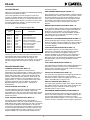
MISCELLANEOUS
WAVEFORM MEMORY
Architecture
Memory Capacity
40ns with 50Ω termination
±0.1% of full scale output
ARBITRARY WAVEFORMS
WAVEFORM CLOCK
Clock Sources
Internal Clock
<10ns (10% to 90%)
<2%, ±30ns (with 50Ω termination)
<5% at full scale output (to 10MHz)
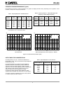
RAMP, TRIANGLE AND ARBITRARY WAVEFORMS
ANALOG FILTERS (EACH CHANNEL)
Number of Filters
Cutoff Frequency
(–3dB down)
Selection
Filter Type
I/O mapped, pluggable to
IBM-PC/AT, PS-30, EISA bus and
compatibles. Decodes eight 16-bit
I/O registers.
Decodes I/O address lines A9
through A4. A3...A0 are decoded
for individual register access.
Highest base address is 3F0 hex.
16-bit I/O transfers; all data is right
justified, offset binary,
sign-extended.
Board reset, clock and trigger
select, timer control, filter select,
offset/gain DAC loading, frequency
synthesizer control, memory
select and load.
Power Requirements
PC/AT bus +5V
PC/AT bus +12V
PC/AT bus –12V
Operating Temp. Range
Storage Temp. Range
Relative Humidity
Altitude
Outline Dimensions
High-speed, static RAM (SRAM)
32,768k x 16 waveform samples
per channel
1. Free run
2. Internal software
programmable triggered
3. External trigger - TTL
4. External gate - TTL
Weight
4
1.6A typical, 2.0A maximum
0.3A typical, 0.4A maximum
0.3A typical, 0.4A maximum
0 to +60°C
–25 to+80°C
10% to 90%, non-condensing
0 to 10,000 feet (0 to 3047m)
4.5"H x 13.31"L x 0.5"W
(11.43 x 33.81 x 1.59cm),
Full size PC/AT board. Uses a
single PC/AT slot.
14oz. (0.42kg)
®