1
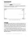
Rev. B
$ 5.00
ANC - 3052/3052B
80C32 Based Embedded Adapter
Antona Corporation, Los Angeles, CA
Antona Corporation
(310)473-8995
FAX
(310)473-7112
Antona Corporation
Copyright
Copyright (c) 1993 by Antona Corporation. All rights reserved. No part of this
publication may be reproduced, transmitted, transcribed, stored in a retrieval system,
or translated into any language or computer language, in any form or by any means,
electronic, mechanical, magnetic, optical, chemical, manual or otherwise, without the
prior written permission of the Antona Corporation of Los Angeles, California.
Warranty
Antona Corporation products are warranted to be free from defects in materials
and workmanship for a period of two (2) years from the date of original shipment to
customer.
This warranty is limited to the replacement or repair of parts not subjected to
misuse, neglect, unauthorized repair, alteration (except card options), accident, or
failure due to the effects of static electricity discharge.
In no event shall Antona Corporation be liable to the purchaser for loss of use,
profit, or consequential damages, or damages of any kind, including, but not limited to,
accidental loss or damage to other equipment, arising out of use of Antona Corporation
equipment, whether or not said equipment was used properly.
This warranty is in lieu of any other warranty, expressed, implied, or statutory,
including, without limitation, any implied warranty or merchantibility or fitness for a
particular purpose. No amendment of this warranty may be effected except in writing
by an officer of the Antona Corporation.
All repair services shall be performed at the Antona Corporation plant in
Los Angeles, Ca.
THE PURCHASER MUST OBTAIN A RETURN
AUTHORIZATION FROM THE ANTONA CORPORATION PRIOR TO
RETURNING ANY PIECE OF EQUIPMENT. Shipment to the Antona Corporation will
be at the expense of the purchaser, return shipment will be at the expense of the Antona
Corporation for all warranty repairs.
Antona Corporation
(310)473-8995 FAX:(310)473-7112
i
TABLE OF CONTENTS
Overview .................................................................................................................................1
Mechanical Specifications ......................................................................................................2
Card Mounting........................................................................................................................2
Card Initialization...................................................................................................................3
Input/Output Addressing.........................................................................................................3
Card Hardware Features........................................................................................................3
Crystal controlled operation...................................................................................................3
8 bit programmable port for parallel digital I/O ....................................................................4
On board memory ...................................................................................................................4
Interrupt handling...................................................................................................................4
Serial Port...............................................................................................................................5
Reset Button ............................................................................................................................5
Power on LED ........................................................................................................................5
Card Jumper Options..............................................................................................................6
JP1 +5v connect to J1 ...........................................................................................................6
JP2 External ROM access .....................................................................................................6
JP3 ROM size select...............................................................................................................6
JP4 RAM Select Memory Space.............................................................................................7
JP5 RS232C input signal to P3.2...........................................................................................7
JP6 RAM Size Select ..............................................................................................................7
JP7 Reset Source Select.........................................................................................................7
JP8 / JP9 Processor Clock Source ........................................................................................7
JP10 RS232C receive data input ...........................................................................................8
External connections to ANC-3052.........................................................................................9
Appendix A - Program listing ...............................................................................................11
Appendix B - I/O and Memory Decode GAL ........................................................................15
Appendix C - BASIC Programming Examples......................................................................17
Appendix D -BASIC ROM Operation ...................................................................................18
Appendix E - Schematic ........................................................................................................23
Antona Corporation
(310)473-8995 FAX:(310)473-7112
ii
Features
♦
♦
♦
♦
♦
♦
♦
♦
♦
♦
♦
80C32 with 11 MHz Crystal controlled operation
Surface mount technology for low power and small size
32K of RAM included on card
32-pin PLCC socket accepts 32K/64K of user supplied ROM
Programmable RS232C level serial port
Decoded lower 8 address bits and PSEN+RD signal for external addressing
memory mapped chip selects for external digital I/0 or additional RAM, decoded
PSN*+RD* to address external RAM as PROM if desired
16 bit crystal controlled counter/timers
bits of programmable I/O
Reset button, Power on LED
Optional internally ROMed Floating Point BASIC interpreter and BASIC up load
utility
Overview
The ANC-3052 combines the best features of a prototyping adapter with the
most commonly needed circuitry to the support the Intel 8032 microcontroller. This
Embedded Adapter™ approach provides the circuit designer with a low cost time
saving method to wire wrap prototype or stand alone systems. Hardware on-board
includes an RS232C level port with 2 user programmable I/O control lines, 8 bits of bidirectional digital I/0 controllable as a single port or by single bits, a 32-pin PLCC
socket to accommodate industry standard byte wide ROM chips, 32K of RAM, 11
interrupts with 2 available externally and 2 16-bit counter/timers for real time interrupts
or counting external events. Although the ANC-3052 was designed to use with Intel's
8052 chip, any 8031,8032,8051,8052,8752 chip will operate with the card. The
designer should locate a copy of the User’s Manual for the 8052 in order to make use
of the microcontroller.
With the ANC-3052B, BASIC version, the user directly enters his program, edits
and after programming with a user supplied PROM programmer, permanently stores to
the on-board PROM in English-like BASIC statements. Upon subsequent system
power-up, the ANC 3052B will perform the previously stored application program. The
CPU card can also act as a slave processor solving complex arithmetic problems
using its FLOATING POINT math, LOG and TRIG functions by letting the user transfer
data to the ANC-3052 and then letting the card solve differential equations, data
reduction analysis, statistics, etc. The 8K BASIC interpreter, based on Intel's 8052
Microcontroller, also features Boolean and string handling functions as well as a realtime clock and interrupt capability. Hardware on-board includes an RS232C level port
to connect to a terminal device for program development or application use.
Antona Corporation
(310)473-8995 FAX:(310)473-7112
1
Mechanical Specifications
Card size, 4.4" X 2.0"
Power requirements = Regulated 5v @ 150ma worse case current
Pin access = on .1" centered rows CPU by 2 40-pin headers, decoded lower address.
& external chip selects by 20-pin header. The RS232 port is accessible by both a 6pin header and a 6-pin modular telephone connector
Figure 2 - Card mounting dimensions (NOT to scale)
Card Mounting
The card may be mounted directly on an Augat type prototyping card, or by
using the enclosed wire/wrap pins, the user can press the pins into his prototype card
super glue or solder them into place, and then insert the ANC-3052 card onto the
receptacle type pins. This allows the user to remove the card for use on other
prototypes or repair (hopefully not necessary). Ribbon cables can also be used to
connect the card to the outside world. Using this approach, the user mounts the card
on the corner standoffs, and then uses short (like 6” or less) of ribbon cable type
connectors to pass the ANC-3082 card’s signals to the users circuitry.
The enclosed labeling sheet allows the user to place pin numbers next to the
wire/wrap pins on the wiring side of the prototype card to help direct the building
process. These really do save time and greatly improve wiring accuracy, but be sure
to double check that the numbering matches the ANC-3052 pin numbers. Pin
numbering of rows is odd on one side and even on the other - standard for
ribbon cable numbering.
Antona Corporation
(310)473-8995 FAX:(310)473-7112
2
Card Initialization
Upon system power-up or a push-button reset, the CPU card's internal system
configuration (i.e. serial baud rate, interrupt enable, etc.) must be performed. A sample
ASSEMBLY LANGUAGE program of a typical initialization routine has been included in
the program listing of Appendix A.
The general procedure for initialization of the card is as follows:
1. Initialization of any external peripheral controller chips.
2. Initialization of the CPU chip's internal characteristics as internal
registers, baud rates, memory, etc.
3. Set up interrupts (if used) for counter/timer, serial port, etc.
4. Transfer control to start execution of user stored program.
The user should become familiar with the internal workings of the 8052 and in
particular, the interfacing with BASIC if using the ANC-3052B card. Note that there are
2 external interrupts inputs on the ANC-3052 on J1 pins for the P3.2 and P3.3
connections. Technical operation of the interrupts can be obtained from the
Microcontrollers User's Manual and the MCS BASIC-52 User's Manual for the ANC3052B (both are Intel Publications).
Input/Output Addressing
Reading or Writing to I/O addresses is performed by memory reads (MOVX
A,@DPTR) or memory writes (MOVX @DPTR,A). The DPTR (Data PoinTeR) is set to
one of the I/O addresses (MOV DPTR,#0F000H for example would select CS1* which
is pin 6 of J3). There are 7 decoded lines available on the 20-pin IDC connector J3.
J3 also provides the ‘or’ed’ signal of PSN* + RD* to use externally connected RAM as
code memory. This is sometimes useful when debugging code by uploading the
program to RAM and then testing it on the actual processor. The user can make
changes to the RAM loaded code much faster than the burn-and-test method using
EPROMs. Just substitute the PSN*+RD* for the RD* signal to the external RAM to
use this capability. A word of warning: There are 8052 instructions which reference
ROM or code space only (MOVC) and there are instructions which reference RAM or
data space only (MOVX). This is how 64K of ROM is differentiated from 64K of RAM.
Remember that debugged code that works perfect in RAM may not work when run
from ROM if these instructions are confused.
Card Hardware Features
Crystal controlled operation
The card is shipped with a crystal frequency of 11.0592 MHz. This is the magic
baud rate frequency to generate serial baud rates up to 38.4 Kbaud. Some
applications may require changing this through hole installed device or using the JP8
and JP9 jumpers to connect an external clock to operate the processor. The installed
80C52 chip will operate up to 16 MHz.
Antona Corporation
(310)473-8995 FAX:(310)473-7112
3
8 bit programmable port for parallel digital I/O
All 8 of the 80C52s port 1 is available for bit level input or output. When using a
pin for input, set the internal bit to a 1. For example to use the upper 4 bits of port 1 for
input execute a “MOV P1,#11110000B” instruction. This would pull the upper 4 bits of
P1 high for external inputs to pull low. While the lower 4 bits of P1 would be pulled low
to control external circuitry. To examine the 4 input lines the user would do a “MOV
A,P1” instruction then examine the 4 upper bits of the accumulator. The input bits are
negative true. When used with BASIC, the user addresses this port as “PORT1”. The
programmer can assign or read this port as if it were a variable (i.e.: PORT1=55H,
PRINT PORT1, A=PORT1 AND 0FH).
On board memory
The card has a 32 pin industry standard memory socket to accommodate 32K
or 64K of EPROM packaged in a 32 pin PLCC type package. ROM is addressed as
code memory starting from 0000H on the ANC-3052, It is addressed as code and data
memory starting at location 8000H on the ANC-3052B BASIC-52 card. At Antona the
devices below have been used on the card successfully:
Manufacturer
Atmel
WSI
Microchip
National Semiconductor
Part Number
AT27C512R-12KC
27C512L-12L
27HC256-90/L
NM27C256V200
Description
EPROM, 64K
EPROM, 64K
ROM, 32K
ROM, 32K
The 32K of on board RAM is addressed as data memory starting from 0000H7FFFH on the ANC-3052B card. The non-BASIC ANC-3052 may address the RAM
from 0000H-7FFFH or 8000H-DFFFH as data RAM (remember E000H to FFFFH is
used by the auxiliary I/O addresses) on the ANC-3052 depending upon the user
selected jumper function of JP4.
Interrupt handling
There is a total of 11 vectored interrupts available to the user, 2 externally and 9
internal to the 80C32. The general procedure for using interrupts is as follows:
1. Enable desired interrupts under software control in initialization.
2. When interrupt is requested, save all registers upon vectored entry.
3. Reset external interrupt latches, reload timers, etc. if needed
4. Input status to determine source of interrupt (may be implicit if there is
only one source associated with the vector)
5. Do interrupt service routine.
6. Restore all registers, re-enable software interrupts and return to main
program.
This sounds a lot harder than it actually is. Refer to the Intel MCS BASIC-52 User’s
Manual for interrupt handling under BASIC control.
Antona Corporation
(310)473-8995 FAX:(310)473-7112
4
Serial Port
The serial port has on board generated RS232C level signals for connection to a
terminal or Pc. Additionally there is a separate RS232C input connectable to P3.2 (see
jumper JP6) and an extra RS232C output connectable to P1.7 (BASIC-52 uses the
P1.7 pin to serially output program listings and data output by an incredible
coincidence). The assembly language user program must monitor and act on these 2
additional lines, they are not controlled by the serial port. BASIC requires that a baud
rate be set to this 2nd serial port before output is possible, If output is directed to the
2nd port line before BAUD is set, the processor will hang up. The BAUD command, as
described in the BASIC-52 User’s Manual, has been tested at Antona with baud rates
up to 38400. If the designer changes the system crystal from 11.0592 MHz, the
“XTAL=“ command is used to inform BASIC of the new frequency (see BAUD
command for details).
Reset Button
Used to reset the internal registers and restart the 80C32 executing program
code from location 0000H.
Power on LED
A neat way to quickly see that the card is powered up properly and may save a
chip from being installed or removed with power applied to the prototype.
Antona Corporation
(310)473-8995 FAX:(310)473-7112
5
Card Jumper Options
Figure 1 - jumper and connector locations
JP1 +5v connect to J1
When installed this jumper connects +5v to pin 40 of J1. User may not want
+5v available on the connector if it is being used for in-circuit emulation. Shipped
disconnected from factory.
JP2 External ROM access
This jumper is used to select internal or external ROM operation. When the
BASIC interpreter is used, this jumper is placed between pins 1 and 2 (as shipped on
ANC-3052B). For accessing external ROM, connect between pins 2 and 3 (as shipped
on ANC-3052).
JP3 ROM size select
Place jumper between pins 1 and 2 for 64K operation (27C512), and between
pins 2 and 3 for 32K (27C256) use. Unless you are doing a mountain of text or lookup
table type programming or using a compiler to generate your code, you will find that the
80C32 does a lot with 6K to 8K of ROM for a typical application. You will need to use a
27C512 if you are EPROMing programs for BASIC. Remember if you are using
BASIC to do a dedicated application that works at power up that BASIC looks for your
ASCII BASIC code starting at 8011H and examines locations 8000H to 8004H for the
type of operation (See Chapter 13 and Appendix A section 1.7, 1.8 in BASIC-52 User’s
Manual).
Antona Corporation
(310)473-8995 FAX:(310)473-7112
6
JP4 RAM Select Memory Space
If the user wishes to map the on board RAM from 8000H to DFFFH providing
24K of RAM, install the jumper between pins 1 and 4. This would be useful if the user
has external RAM which is desired to be in the lower half of the memory space.
Installing the jumper between pins 1 and 3 addresses the on board RAM as 0000H to
7FFFH (32K) in the processor’s RAM space (as shipped, and required for BASIC
operation). Jumpering between pins 1 and 2 completely disables the on board RAM.
Some applications for the 80C32 do not require external RAM, just the internal 256
bytes of bit, register and scratch pad RAM. Note that the common pin is the one
isolated on the left of the Version A circuit board. The shunt will work with a little
effert.
JP5 RS232C input signal to P3.2
Installing this jumper connects the 2nd RS232C input pin, which can be used as
a ready to send (RTS) signal to the 80C32 processor or as a second RS232C serial
input port with a ‘bit-banged’ software processor. Note that the processor pin - P3.2 on
the 80C32 can generate an interrupt (INTR 0*) on this input signal. Shipped NOT
connected.
JP6 RAM Size Select
The ANC-3052 is now shipped with 32K of 8-bit RAM, which means the jumper
should normally be placed between pins 1 and 2 (as shipped). Jumpering between
pins 2 and 3 would allow a smaller 8K RAM chip to be used (see jumper JP4 also).
The only use this jumper now has is to limit the on board RAM size if the designer
desired a special purpose RAM for the particular application (dual port RAM, etc.).
JP7 Reset Source Select
To use the on board push button reset, connect jumper between pins 1 and 2
(as shipped). To remotely reset processor through J1 connector, connect jumper
between pins 2 and 3. This feature is useful if the user desires to remotely restart
program operation, like from a front panel push button. The user may also implement a
watchdog timer externally to restart program operation if the processor stops writing to
one of the external I/O lines. The reset signal is a positive pulse, and is required for
proper operation to be generated after power up by either the on board circuitry or a
user supplied external source.
JP8 / JP9 Processor Clock Source
These jumpers disconnect the on board 11.0592 MHz crystal so that an external
clock or crystal may be used. When using an external crystal, wire length must be
kept short and this mode of operation is not recommended. More commonly, an
external TTL or CMOS level clock is driven to the XT1 input. Connect both sets of
jumpers between pins 1 and 2 for on board crystal operation (as shipped) or both
jumpers between pins 2 and 3 for external clock operation.
Antona Corporation
(310)473-8995 FAX:(310)473-7112
7
JP10 RS232C receive data input
The user may desire to disconnect the RS232C input element to the 8032’s
UART to use an alternate type of serial interface (like RS422). Install this jumper to
connect the RS232C element for input (as shipped).
Antona Corporation
(310)473-8995 FAX:(310)473-7112
8
External connections to ANC-3052
40 pin IDC - 80C32 Processor Signals
J1 PIN CONN
8032 FUNCTION
USER IDENTIFICATION
40
+5 VOLTS
+5 volts to J2 for powering external chips
38
A8
36
A9
34
A10
32
A11
30
A12
28
A13
26
A14
24
A15
22
PSE
20
ALE
18
-not connectedexternal / internal ROM select (JP2)
16
D0
14
D1
12
D2
10
D3
8
D4
6
D5
4
D6
2
D7
40 pin IDC - 80C32 Processor Signals
J2 PIN CONN
8032 FUNCTION
USER IDENTIFICATION
40
P1.0
38
P1.1
36
P1.2
34
P1.3
32
P1.4
30
P1.5
28
P1.6
26
P1.7
24
RST (reset 80C32)
22
REC (serial receive)
20
TXD (serial xmit)
18
P3.2 / INTR 0*
16
P3.3 / INTR 1*
14
P3.4 / COUNT 0*
12
P3.5 / COUNT 1*
10
WR* (write extn)
8
RD* (read extn)
6
XT2
4
XT1
External processor clock input
2
GROUND
GROUND
Note: all ODD numbered pins on J1 and J2 connect to GROUND
Antona Corporation
(310)473-8995 FAX:(310)473-7112
9
20 pin IDC Auxiliary Control and Address Lines
J3 PIN CONN
PIN DEFINITION
USER DEFINITION
19
+5 VOLT
+5 volts for driving external circuitry
17
A7
15
A6
13
A5
11
A4
9
A3
7
A2
5
A1
3
A0
1
GROUND
ground for J3
20
18
16
14
12
10
8
6
4 (ANC-3052)
4 (ANC-3052B)
2
+5 VOLT
RAM* (PSN*+RD*)
CS6* (E400H-E7FFH)
CS5* (E000H-E3FFH)
CS4* (FC00H-FFFFH)
CS3* (F800H-FBFFH)
CS2* (F400H-F7FFH)
CS1* (F000H-F3FFH)
CS0* (8000H-DFFFH)
CS0* (0000H-DFFFH
as code and 8000HDFFFH-as data)
GROUND
6 pin single inline connector
J4 PIN CONN
PIN DEFINITION
1
GROUND
2
GROUND
3
CTS
4
RTS
5
TXD
6
RCD
6 pin modular phone connector
J5 PIN CONN
PIN DEFINITION
1
GROUND
2
TXD
3
RTS
4
RCD
5
CTS
6
GROUND
2 pin .025 inch square posts
J6 PIN CONN
PIN DEFINITION
1
+5 VOLTS
2
GROUND
Antona Corporation
+5 volts for driving external circuitry
RD* on external RAM to addr as PROM
used to control the ROM socket on
BASIC-52 version of card
ground for J3
USER DEFINITION
ground for J4
ground for J4
USER DEFINITION
ground for J5
ground for J5
USER DEFINITION
POWER TO CARD
GROUND TO CARD
(310)473-8995 FAX:(310)473-7112
10
Appendix A - Program listing
Initialization - This process is probably the hardest part of using the 80C52.
Below is a sample listing of a typical initialization routine which you may tailor to fit your
application. This listing is a small piece of a complete application program using the
ANC-3052. Your program will almost certainly need to do additional setup and some of
the steps listed here, of course, will not be needed. The program uses the Intel MCS51 Macro Assembler pseudo op codes which vary with assemblers. No warranty is
expressed or implied by the use of this code, it is provided as a sample from which the
user may build upon. The program equates are included to help the designer better
visualize the process.
; PROGRAM EQUATES
; MEMORY AND I/O
BEGPRG
PCODE
EXTMEM
INTBT
INTRM
EQU
EQU
EQU
EQU
EQU
0000H
002CH
8000H
00H
30H
;BEG. PROGRAM
;PROGRAM CODE
;EXTERNAL RAM
;INTERN AL BEG OF BIT RAM
;INTERNAL BEG. OF RAM
;**************************************************************************
; EXTERNAL 16 BIT EQUATES
SELET
CHOPR
CHPLD
DIPIN
EQU
EQU
EQU
EQU
0F000H
0F000H
0F001H
0F002H
;AUX SELECT ADDRS
;CHOPPER COUNT
;RESET CHOPPER COUNT
;8-BIT USER SWITCH
RSTLED EQU
SDCLK EQU
0F003H
0F004H
;RESET LED DISPLAY
;PULSE SERIAL DATA TO LED
LATCH EQU
0E000H
;8-BIT LATCH OUTPUT
ADC
DAC
0E000H
0E400H
;ANALOG TO DIGITAL BASE ADDR
;DIGITAL TO ANALOG BAS E ADDR
0F400H
MCPADR
MCPADR+1
MCPADR+2
MCPADR+3
;8255 BASE ADDR
EQU
EQU
MCPADR EQU
PORTA EQU
PORTB EQU
PORTC EQU
MCPIO EQU
; INTERNAL 8 BIT EQUATES
STABLE EQU
CR
EQU
20
0DH
;20 MS DEBOUNCE FOR DISCRETE SWITCHES
;CARRIAGE RETURN
; INTERNAL 16 BIT EQUATES
MS1
EQU
-922
MS50
SEC1
EQU
EQU
50
1000
;APPROX 1 MS RELOAD VALUE, NUMBER IS
;COUNT REQUIRED WITH 11.0592MHZ / 12
;TIME RATE FOR .0010004 MS INTERRUPT
;50 MS DELAY
;1 SEC (NUMBER OF 1MS TO FORM 1 SEC)
; MASK BIT SET
Antona Corporation
(310)473-8995 FAX:(310)473-7112
11
BIT0
BIT1
BIT2
BIT3
BIT4
BIT5
BIT6
BIT7
EQU
EQU
EQU
EQU
EQU
EQU
EQU
EQU
00000001B
00000010B
00000100B
00001000B
00010000B
00100000B
01000000B
10000000B
MOT0
MOT1
MOT2
MOT3
MOT4
MOT5
MOT6
MOT7
EQU
EQU
EQU
EQU
EQU
EQU
EQU
EQU
11111110B
11111101B
11111011B
11110111B
11101111B
11011111B
10111111B
01111111B
ROW0
ROW1
ROW2
ROW3
ROW4
ROW5
EQU
EQU
EQU
EQU
EQU
EQU
00000000B
00100000B
01000000B
01100000B
10000000B
10100000B
SAVUP EQU
SAVLW EQU
0F0H
0FH
;STANDARD MASKS FOR UPR/LWR NIBBLE
; INTERNAL DATA BIT STORAGE, BIT-MEMORY
BITFG EQU
INTBT
;INTERNAL BEG. OF BIT RAM
SWTDN
TIMUP
LEDFG
CHRFG
SENFG
SNRFG
EQU
EQU
EQU
EQU
EQU
EQU
BITFG+0
BITFG+1
BITFG+2
BITFG+3
BITFG+4
BITFG+5
VSEN
EQU
BITFG+10
;ANY BUTTON DOWN, AND ACTED ON
;TIME-OUT TIMER HAS COMPLETED CYCLE
;LED BYTE TO OUTPUT TIME FLAG
;DOING DISPLAY UPDATE
;PHOTONS DETECTED
;STABLE INPUT CHECK
;FLAG FOR LOW VOLTAGE SENSE
; INTERNAL BYTE DATA STORAGE
RAMBG EQU
INTRM
;INTERNAL BEG. OF REGISTER RAM
HITFG
SPSW
QLTS
TFLG
MSH
MSL
INERR
INFLG
OTFLG
DINL
DOTL
BFEXB
BFMSB
BFM
BFLSB
SWIT
DIP
FMSB
FM
FLSB
RAMBG
RAMBG+1
RAMBG+2
RAMBG+3
RAMBG+4
RAMBG+5
RAMBG+6
RAMBG+7
RAMBG+8
RAMBG+9
RAMBG+0AH
RAMBG+0BH
RAMBG+0CH
RAMBG+0DH
RAMBG+0EH
RAMBG+0FH
RAMBG+10H
RAMBG+11H
RAMBG+12H
RAMBG+13H
;DISCRETE SWITCH HIT FLAG
;SAVED PSW (USE D FOR PARITY CHECK)
;TIMES SWITCHES STAYED THE SAME
;ENABLE TIMEOUT ERROR CHECK FOR COMM.
;UPR 8 BITS OF TIMEOUT TIMER
;LWR - 16 BIT TIMER 1 TICK = 1MS
;SERIAL PARITY ERROR COUNTER
;SERIAL INPUT MESSAGE COMPLETE = BIT7 HIGH
;SERIAL OUTPUT MESSAGE DONE = 00H
;MEM PTR OF ASCII INPUT MESSAGE
;MEM PTR OF ASCII OUTPUT MESSAGE
;EXTENDED BYTE
EQU
EQU
EQU
EQU
EQU
EQU
EQU
EQU
EQU
EQU
EQU
EQU
EQU
EQU
EQU
EQU
EQU
EQU
EQU
EQU
Antona Corporation
;FOOTAGE COUNT - BINARY
;DISCRETE SWITCHES
;USER DIP SWITCH
;FOOTAGE COUNT - PROCESSED FOR OUTPUT
(310)473-8995 FAX:(310)473-7112
12
BLKFG
CHRCT
LEDBF
LDEND
ASCPT
EQU
EQU
EQU
EQU
EQU
RAMBG+18H
RAMBG+2FH
RAMBG+30H
RAMBG+38H
RAMBG+38H
;BLINK ENABLE FLAG
;CURRENT CHAR BEING OUTPUT TO LED
;LED DISPLAY BUFFER
;END OF BUFFER MARKER
;5 BYTE PATTERN OF ASCII BYTE
BUFBG EQU
RAMB G+40H
;MOVE AWAY FROM OTHERS
DATAI EQU
DATAX EQU
BUFBG
BUFBG+9
;CURRENT SERIAL DATA BEING INPUT
;CURRENT SERIAL DATA BEING XMITTED
STACK EQU
0E0H
;//STACK STARTING LOC//
; EXTERNAL DATA STORAGE
$EJECT
; CODE BEGINS HERE
ORG
BEGPRG
START:LJMP PWRON
;POWER ON SEQUENCE
ORG
BEGPRG+3
EXT0INT:RETI
;External Interrupt 0 Vector
;Pin 12 LOW - NOT USED
ORG
BEGPRG+0BH
HPDRV:LJMP T0INT
;TIMER/COUNTER 0 VECTOR
;1MS REAL TIME INTERRUPT
ORG
EXI1V:
;External Interrupt 1 Vector
;do nothing for Ext 1
BEGPRG+13H
RETI
ORG
BEGPRG+1BH
EXT1INT: RETI
;TIMER/COUNTER 1 VECTOR
; T1 is used for Serial clock
ORG
SERI: LJMP
BEGPRG+23H
SERIAL
;SERIAL INTERRUPT VECTOR
ORG
RETI
BEGPRG+2BH
;Timer/Counter 2 Vector
;T2 only exists in the 8052
ORG
PCODE
PWRUP:
DB
'8032 V1.0'
;POWER UP SIGN ON
; POWER UP INITIALIZATION
PWRON:MOV
MOV
IE,#00000000B
SP,#STACK
;DISABLE ALL INTERRUPTS
;Hdw Reset, SET STACK
MOV
PSW,#00000000B
;INITIALIZE STATUS WORD
MOV
MOV
MOVX
DPTR,#MCPIO
A,#93H
@DPTR,A
;INIT SET UP OF ON BOARD 8255
;DEFAULT CONFIGURATION
MOV
MOV
MOVX
MOV
MOVX
A,#00H
DPL,#LOW(PORTC)
@DPTR,A
DPL,#LOW(CHPLD)
@DPTR,A
Antona Corporation
;ENABLE EXTERNAL BUS
;PRESET EXTERNAL SYNC COUNT = 0
(310)473-8995 FAX:(310)473-7112
13
MOV
MOV
R0,#RAMBG
A,#00H
ICLR: MOV
INC
CJNE
@R0,A
R0
R0,#00,ICLR
MOV
CLEAN:MOVX
INC
DJNZ
DPTR,#EXTMEM
@DPTR,A
DPTR
R0,CLEAN
;CLEAR INTERNAL RAM
;CLEAR 1ST 256 LOCS IN MEM.
;R0 WAS SET TO 00 FROM ABOVE
MOV
MOVX
MOV
DPTR,#DIPIN
A,@DPTR
DIP,A
;READ IN DIP SWITCH
MOV
BFLSB,#02H
;PRESET INTERNAL COUNT FRACTION
MOV
MOVX
DPTR,#CHOPR
A,@DPTR
;DUMMY READ TO CLEAR CHOPPER PORT
MOV
MOV
DINL,#DATAI
DOTL,#DATAX
;INITIALIZE SERIAL IN/OUT PTRS.
SETB
PT0
;PUT REAL TIME AS HIGHER INTR.
MOV
MOV
P1,#11111011B
TMOD,#00100001B
;INITIALIZE P1, TURN ON LED
;TMR 0 =16BIT,TMR 1 = AUTO RELOAD
MOV
MOV
MOV
TH1,#-3
TL1,#-3
SCON,#01011000B
;9600 RATE = -(11.0592MHZ/(384*9600))
;SET TO SAME COUNT
;MODE 3, REN ON,RI ON, 8-BIT,NP,1-STP
MOV
MOV
TL0,#LOW(MS1)
TH0,#HIGH(MS1)
;SETUP TIMER 0 FOR 1MS INTERRUPT
MOV
TCON,#01010000B
;TURN ON TIMER 0 AND 1
;WILL READ BACK FROM HERE ONLY
; WRITE PWR-UP MESSAGE TO SIEMENS 8 CHAR DISPLAY
MOV
DPTR,#PWRUP
LCALL XLEDBF
SETB LEDFG
;STANDARD PWR UP MESSAGE
;XFER TO LED BUFFER
;QUEUE UP MESSAGE OUTPUT
MOV
MOV
;DUMMY READ TO EMPTY INPUT BUFR
;TURN ON INTERRUPTS,(EA,ES,ET0)
A,SBUF
IE,#10010010B
; MAIN PROGRAM LOOP IS HERE
EXEC:LCALL RECV
;COMPLETED INPUT MESSAGE?
LCALL ANAL
;ANALYZE SENSOR INPUT DATA
LCALL LEDDRV
;DRIVE LED DISPLAY
LCALL HOUSKP
;DO ANY HOUSEKEEPING FUNCTIONS
SJMP EXEC
; (body of the program,‘EXEC’ called processes and subroutines)
END
;END OF PROGRAM
Antona Corporation
(310)473-8995 FAX:(310)473-7112
14
Appendix B - I/O and Memory Decode GAL
The external decoding of addresses generated by the 80C32 is performed by a
single chip; a Generic Array Logic device or GAL for short. The advanced user may
desire to change the address space and/or the way that memory and I/O are decoded.
Following are the equations currently used on the ANC-3052 card. Some applications
require that the WR* and RD* signal not be connected to chip select. Note that CS0*
which decodes from 8000H through DFFFH is not conditioned upon either RD* or
WR*. You may also change the GAL equations and program a new part or just use the
raw address lines on J2 to generate the desired address select off the ANC-3052
circuit board. The format for the equations below is for National Semiconductor’s
PLANII GAL compiler.
title
pattern
revision
author
company
date
Antona 3052 Memory and I/O Address Decode
A3052
F
Robert Mikkelson
Antona Corporation
06/22/94
chip A3052 gal16v8
; pin
1
2
3
4
5
6
7
8
9 10
RDN ALE PSN A14 A10 WRN A12 A13 A11 GND
; pin
11 12 13 14 15 16 17 18 19 20
A15 CS0 CS1 CS2 CS3 CS4 CS5 CS6 RAM VCC
; Electronic signature for this part - "ANTONA #02"
@UES ATC02
equations
/RAM = /PSN + /RDN
; CS0* SELECTED BY 8000H-DFFFH ONLY
/CS0 = A15 * /A14 * /A13 +
A15 * /A14 * A13 +
A15 * A14 * /A13 +
A15 * /A14 * /A13
/CS1 = A15 * A14 * A13 * A12 * /A11 * /A10 * /WRN +
A15 * A14 * A13 * A12 * /A11 * /A10 * /RDN
/CS2 = A15 * A14 * A13 * A12 * /A11 * A10 * /WRN +
A15 * A14 * A13 * A12 * /A11 * A10 * /RDN
/CS3 = A15 * A14 * A13 * A12 * A11 * /A10 * /WRN +
A15 * A14 * A13 * A12 * A11 * /A10 * /RDN
/CS4 = A15 * A14 * A13 * A12 * A11 * A10 * /WRN +
A15 * A14 * A13 * A12 * A11 * A10 * /RDN
/CS5 = A15 * A14 * A13 * /A12 * /A11 * /A10 * /WRN +
A15 * A14 * A13 * /A12 * /A11 * /A10 * /RDN
/CS6 = A15 * A14 * A13 * /A12 * /A11 * A10 * /WRN +
A15 * A14 * A13 * /A12 * /A11 * A10 * /RDN
; end of file
The following equations are used for the GAL on the BASIC version of the card:
Antona Corporation
(310)473-8995 FAX:(310)473-7112
15
title
pattern
revision
author
company
date
Antona 3052 Memory and I/O Address Decode for BASIC-52
B3052
C
Robert Mikkelson
Antona Corporation
03/22/94
chip B3052 gal16v8
; pin
1
2
3
4
5
6
7
8
9 10
RDN ALE PSN A14 A10 WRN A12 A13 A11 GND
; pin
11 12 13 14 15 16 17 18 19 20
A15 CS0 CS1 CS2 CS3 CS4 CS5 CS6 RAM VCC
; Electronic signature for this part - "ANTONA #03"
@UES ATC03
equations
/RAM = /PSN + /RDN
; CS0* TO PROM SOCKET: 8000H-DFFFH WITH RD* (BASIC PROGRAMS)
;
0000H-DFFFH WITH PGN* (ASSEMBLY LANGUAGE)
/CS0 = /PSN * /A15+
/PSN * A15 * /A14 * /A13 +
/PSN * A15 * /A14 * A13 +
/PSN * A15 * A14 * /A13 +
/RDN * A15 * /A14 * /A13 +
/RDN * A15 * /A14 * A13 +
/RDN * A15 * A14 * /A13
/CS1 = A15 * A14 * A13 * A12 * /A11 * /A10 * /WRN +
A15 * A14 * A13 * A12 * /A11 * /A10 * /RDN
/CS2 = A15 * A14 * A13 * A12 * /A11 * A10 * /WRN +
A15 * A14 * A13 * A12 * /A11 * A10 * /RDN
/CS3 = A15 * A14 * A13 * A12 * A11 * /A10 * /WRN +
A15 * A14 * A13 * A12 * A11 * /A10 * /RDN
/CS4 = A15 * A14 * A13 * A12 * A11 * A10 * /WRN +
A15 * A14 * A13 * A12 * A11 * A10 * /RDN
/CS5 = A15 * A14 * A13 * /A12 * /A11 * /A10 * /WRN +
A15 * A14 * A13 * /A12 * /A11 * /A10 * /RDN
/CS6 = A15 * A14 * A13 * /A12 * /A11 * A10 * /WRN +
A15 * A14 * A13 * /A12 * /A11 * A10 * /RDN
; end of file
Antona Corporation
(310)473-8995 FAX:(310)473-7112
16
Appendix C - BASIC Programming Examples
The short listings that follow give the ANC-3052B user an idea of the cards
capability to quickly implement an application. These listings are sample programs
only, and are intended as a guide for the designer to build upon.
10
20
30
40
50
60
REM SAMPLE INITIALIZATION OF ANC-3052 CARD
REM
MTOP=MTOP-0FFH
BAUD 9600
PRINT “ANTONA Corporation”
END
10
20
30
40
60
70
80
REM EXERCISE ONBOARD PORT 1
REM
FOR X=0 TO 0FFH
PORT1=X
NEXT X
GOTO 30
END
20
30
35
40
50
60
70
80
85
90
100
110
120
130
140
REM HEX DUMP MEMORY PROGRAM
REM USE TO EXAMINE DATA AND MEMORY MAPED I/O
REM
INPUT “ENTER BEG. ADDR. IN HEX=“,V
FOR X=0 TO 0FH
PH0. V,” “,
FOR Y=0 TO 0FH
PH0. XBY(V+Y),
IF Y=7 THEN PRINT “ “,
NEXT Y
PRINT
V=V+10H
NEXT X
PRINT
GOTO 40
Antona Corporation
(310)473-8995 FAX:(310)473-7112
17
Appendix D -BASIC ROM Operation
This ability makes BASIC more than just a fast way to check out hardware or
test an idea for a program. It makes the ANC-3052B into the finished product. The
designer can store a program to an externally programmed ROM, and then have the
ANC-3052B perform that set of BASIC commands upon power up. To the outside
world, the processor looks like a dedicated embedded system. The process is as
follows:
• The IBM Pc compatible disk enclosed contains a file called “DMPBAS.HEX”. The
user needs to download this file to a suitable PROM programmer and program a
27C512 with this code. Install the 27C512 in the ANC-3052B PROM socket
• Enter your source BASIC code initially into a Pc based editor capable of plain ASCII
text input/output (like Word or WordPerfect).
• Use a terminal program on the Pc to download and debug your application program
in BASIC. Saving the work-in-progress BASIC code is highly recommended using
the upload function of the terminal program. I like to save the files to disk under
different file names in case I need to ‘resurrect’ an earlier version of the program.
• Upload the tokenized source BASIC program from the ANC-3052B card (in HEX) to
the Pc. This is done by evoking the save-to-disk (upload) function from the terminal
program and running the DMPBAS program below from ROM on the ANC-3052B
card to convert and send the RAM based user application BASIC code to the Pc in
Intel HEX format readable by a PROM programmer. After installing the 27C512 in
the ANC-3052B PROM socket as described above, typing RROM (Run ROMed
program 1) will read your RAM entered BASIC program and transmit the tokenized
code in formatted HEX. Usually the user must terminate the save-to-disk terminal
function by pressing some key (like Esc) or combination of keys on the Pc. Before
sending the file to a PROM programmer, the user will need to load the HEX file into
a suitable editor and delete the extra lines at the beginning and ending of the file.
This program does 99% of the process for setting up a single BASIC application
program from location 200H in RAM to ROM starting at location 8010H. The user
must look at the various PROG 1-6 commands to decide which is appropriate for
the application. Run mode 4 sets the BAUD RATE, MTOP and then executes the
user’s code without transmitting the BASIC sign on message. Remember that
BASIC “REM”, remark lines, take time to execute in BASIC so you might want to
erase or put any comments beyond the “END” statement in your code.
LIST
10
20
30
40
100
110
112
114
115
120
130
135
REM
REM INTEL HEX FILE OF BASIC-52 RAM
REM REV. C, 1994
REM
REM
REM SET RUN MODE, BAUD, MTOP
REM
STRING 3,1
PRINT "SELECT RUN-MODE TYPE, 1 CHAR. ",
INPUT "(ENTER 0 FOR COMMAND MODE) = ",R
PRINT "SET BAUD RATE IN BITS/SEC ",
INPUT "(ENTER 0 FOR AUTOBAUD) = ",B
Antona Corporation
(310)473-8995 FAX:(310)473-7112
18
138
140
200
210
220
230
240
250
260
270
275
280
300
310
320
330
340
350
360
365
370
380
390
400
410
420
430
440
450
500
510
520
530
540
550
600
610
620
630
640
650
660
1020
1030
1032
1034
1036
1038
1039
1040
1042
1044
1050
1082
1084
1090
1100
1104
1106
1110
1115
1120
1170
1172
IF B=0 THEN S=0FFFFH : GOTO 200
S=65536-(XTAL/(32*B))
PRINT "SET HEX MTOP VALUE ",
INPUT "(ENTER 0FFFFH FOR NOT-SET) = ",T
PRINT "SET PROM LOAD ADDRESS FOR HEX FILE"
INPUT "ENTER 0 FOR 8010H (ADDR. IN HEX) = ",A
IF A>0 THEN H=(A/100H).AND.0FFH : L=A.AND.0FFH : GOTO 260
H=80H : L=10H
V=1FFH
PRINT "" : PRINT "START TERMINAL UPLOAD, ",
INPUT "THEN PRESS ENTER ",$(0)
PRINT "" : PRINT ""
PRINT ":10",
B=80H
GOSUB 2100
B=00H
GOSUB 2100
PRINT "00",
C=90H
IF R=0 THEN R=0FFH
B=R.OR.30H
C=C+B
GOSUB 2100
B=(S/100H).AND.0FFH
C=C+B
GOSUB 2100
B=S.AND.0FFH
C=C+B
GOSUB 2100
B=(T/100H).AND.0FFH
C=C+B
GOSUB 2100
B=T.AND.0FFH
C=C+B
GOSUB 2100
FOR P=5 TO 0FH
C=C+0FFH
PRINT "FF",
NEXT P
B=((0FFFFH-C).AND.0FFH)+1
GOSUB 2100
PRINT ""
C=H+L+10H
PRINT ":10",
B=H
GOSUB 2100
B=L
GOSUB 2100
PRINT "00",
FOR X=0 TO 0FH
B=XBY(V+X)
IF V+X=1FFH THEN B=55H
C=C+B
GOSUB 2100
IF (B=1).AND.(XBY(V+X-1)=0DH).AND.(XBY(V+X+1)=0) THEN GOTO 1200
NEXT X
B=((0FFFFH-C).AND.0FFH)+1
GOSUB 2100
PRINT ""
V=V+10H
L=(L+10H).AND.0FFH : IF L=0 THEN H=(H+1).AND.0FFH
GOTO 1020
REM
REM FOUND THE END OF FILE CHAR
Antona Corporation
(310)473-8995 FAX:(310)473-7112
19
1174
1176
1200
1205
1210
1215
1220
1222
1224
1230
1240
1250
2000
2010
2020
2030
2100
2110
2120
2210
2230
2240
2250
2260
•
•
REM SO FINISH UP LINE AND OUTPUT END-OF-FILE
REM
IF X=0FH THEN GOTO 1222
FOR P=X+1 TO 0FH
C=C+0FFH
PRINT "FF",
NEXT P
B=((0FFFFH-C).AND.0FFH)+1
GOSUB 2100
PRINT ""
PRINT ":00000001FF"
END
REM
REM TURN BYTE (B) INTO 2 ASCII CHARS N,M
REM AND OUTPUT THEM TO CONSOLE
REM
N=(B/10H).OR.30H
IF N>39H THEN N=N+07H
PRINT CHR(N),
M=(B.AND.0FH).OR.30H
IF M>39H THEN M=M+07H
PRINT CHR(M),
RETURN
REM -END OF FILE-
The user can save additional BASIC programs by locating the end-of-file (01H)
within the user’s PROM, setting the LOAD ADDRESS to follow the 01H char in
PROM and deleting the first line of the generated HEX file that contains the
startup information.
The DMPBAS program will prompt you to enter the desired RUN mode, BAUD
RATE and MTOP. If you are using a crystal frequency other than the 11.0592
MHz shipped on the ANC-3052 card, you must assign the XTAL default value to
your crystal frequency before running the DMPBAS program.
Typing
“XTAL=12000000” within the BASIC-52 command mode would set XTAL for a
12 MHz crystal to calculate BAUD rate values. The lines are then converted
into HEX lines. This information is located physically on the ROM from location
8000H to 8004H. Set these locations to 0FFH if automatic run, baud rate setting
and/or MTOP setting is NOT desired at power on or reset time. Locations
8005H to 800FH are set to 0FFH in any event. The following lines are actual
output from the DMPBAS program of the DMPBAS source code The underlined
characters are user entered data. The procedure below is how the designer
would generate the HEX file for the DMPBAS PROM used to upload the
developed application program:
READY
>RROM ↵
SELECT RUN-MODE TYPE, 1 CHAR. (ENTER 0 FOR COMMAND MODE) =
SET BAUD RATE IN BITS/SEC (ENTER 0 FOR AUTOBAUD) =
0↵
SET HEX MTOP VALUE (ENTER 0FFFFH FOR NOT-SET) =
0FFFFH ↵
SET PROM LOAD ADDRESS FOR HEX FILE
ENTER 0 FOR 8010H (ADDR. IN HEX) =
0↵
START TERMINAL UPLOAD, THEN PRESS ENTER
Antona Corporation
0↵
(start upload function)↵
(310)473-8995 FAX:(310)473-7112
20
:10800000FFFFFFFFFFFFFFFFFFFFFFFFFFFFFFFF80
:108010005505000A960D2400149620494E54454CEF
:10802000204845582046494C45204F462042415360
:1080300049432D35322052414D0D12001E962052DB
body of HEX file
:1085F0000D09084889D34E292C0D1108A24DEAE037
:1086000042E730464829E83330480D1208B69E4DFF
:10861000EF333948A54DEA4DE33037480D0908C01E
:1086200089D34D292C0D0508CA9D0D1308D4962019
:108630002D454E44204F462046494C452D0D01FF07
:00000001FF
READY
>
Sample BASIC-52 Run Mode Program
The following short BASIC-52 program was entered, uploaded to a Pc, a PROM cut
with the HEX file generated below, installed on the ANC-3052B card and executed.
10
20
30
40
50
60
70
80
90
100
REM
REM SET RUN MODE 4, BAUD 9600, MTOP 7EFFH
REM
PRINT ""
PRINT "HELLO WORLD"
PRINT ""
PH0. "RUN MODE =",XBY(8000H),", RCAP2 =",RCAP2,
PH0. ", MTOP =",MTOP
END
REM -END OF FILE-
READY
>RROM ↵
SELECT RUN-MODE TYPE, 1 CHAR. (ENTER 0 FOR COMMAND MODE) =
SET BAUD RATE IN BITS/SEC (ENTER 0 FOR AUTOBAUD) =
9600 ↵
SET HEX MTOP VALUE (ENTER 0FFFFH FOR NOT-SET) =
7EFFH ↵
SET PROM LOAD ADDRESS FOR HEX FILE
ENTER 0 FOR 8010H (ADDR. IN HEX) =
0↵
START TERMINAL UPLOAD, THEN PRESS ENTER
4↵
(start upload function)↵
:1080000034FFDC7EFFFFFFFFFFFFFFFFFFFFFFFFEF
:108010005505000A960D2B00149620534554205206
:10802000554E204D4F444520342C2042415544208C
:10803000393630302C204D544F5020374546464875
:108040000D05001E960D0700288922220D12003210
:10805000892248454C4C4F20574F524C44220D0723
:10806000003C8922220D290046852252554E204D82
:108070004F4445203D222CBDE03830303048292C7B
:10808000222C205243415032203D222CCE2C0D1167
:10809000005085222C204D544F50203D222CC40DE1
:1080A00005005AA30D13006496202D454E44204F21
:1080B000462046494C452D0D01FFFFFFFFFFFFFF06
:00000001FF
READY
>
Antona Corporation
(310)473-8995 FAX:(310)473-7112
21
Power-on output from the ANC-3052B card after PROM with the HEX file installed (Pc
terminal was set to receive 9600 baud):
HELLO WORLD
RUN MODE = 34H, RCAP2 = FFDCH, MTOP = 7EFFH
READY
>
Program run mode is 4 (34H), baud rate set to 9600 by the 0FFDCH count up value in
the 16-bit RCAP2 counter and RAM has been preserved above 7EFFH (RAM from 0000H 7EFFH has been set to 00H).
Antona Corporation
(310)473-8995 FAX:(310)473-7112
22
Appendix E - Schematic
The following “A” size sheets are the circuit board schematics for the version-A
ANC-3052 and ANC-3052B card.
Antona Corporation
(310)473-8995 FAX:(310)473-7112
23