1
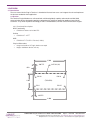
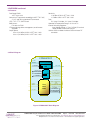
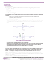
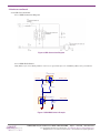
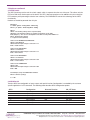
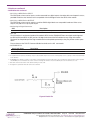
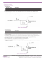
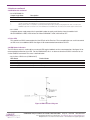
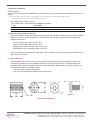
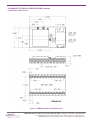
CDMA910CF Terminus
Plug-In Products User Manual
Bulletin
Revision
Date
JA03-UM-CDMA
P01
17 July 2014
TABLE OF CONTENTS
TABLE OF CONTENTS and DISCLAIMER.............................................................................................................................. 2
1 APPLICABILITY TABLE........................................................................................................................................................ 3
2 REFERENCES...................................................................................................................................................................... 3
2.1 Telit Document List.................................................................................................................................................. 3
3 OVERVIEW............................................................................................................................................................................ 4
3.1 Introduction............................................................................................................................................................. 4
3.2 Preview.................................................................................................................................................................... 4
3.3 CDMA Features....................................................................................................................................................... 5
3.4 CDMA Block Diagram............................................................................................................................................. 5
4 INTERFACES................................................................................................................................................................... 6-14
4.1 Serial Interface...................................................................................................................................................... 6-7
4.2 Power Supply.......................................................................................................................................................... 7
4.3 Audio Interface........................................................................................................................................................ 8
4.4 Plug-In Pin-Out........................................................................................................................................................ 9
4.5 VRTC Details.......................................................................................................................................................... 10
4.6 GPIO Details..................................................................................................................................................... 10-13
4.7 User LED................................................................................................................................................................ 13
4.8 LED Status Indicators........................................................................................................................................... 13
4.9 RF Interface........................................................................................................................................................... 14
4.10 Header Interface Mounting Options..................................................................................................................... 14
4.11 Screw Mounting.................................................................................................................................................... 14
5 CDMA910CF TECHNICAL SPECIFICATIONS.............................................................................................................. 15-23
5.1 Electrical Specifications................................................................................................................................... 15-17
5.2 CDMA Mechanical Specifications........................................................................................................................ 18
5.3 Setting Up a Terminal Emulator for use with the CDMA910CF Terminus...................................................... 19-20
6 DESIGN CONSIDERATIONS.............................................................................................................................................. 21
6.1 Minimum Required Module Pin Connects........................................................................................................... 21
6.2 Debug..................................................................................................................................................................... 21
APPENDICES........................................................................................................................................................................ 22
Approvals............................................................................................................................................................... 22
Safety..................................................................................................................................................................... 22
Antenna Care and Replacement........................................................................................................................... 22
Abbreviations......................................................................................................................................................... 22
Ordering Information............................................................................................................................................. 23
Revision History..................................................................................................................................................... 23
DISCLAIMER
The information contained in this document is the proprietary information of Connor-Winfield Corporation and its affiliates (Janus Remote Communication). The contents are confidential and any disclosure to
persons other than the officers, employees, agents or subcontractors of the owner or licensee of this document, without the prior written consent of Connor-Winfield, is strictly prohibited. Connor-Winfield
makes every effort to ensure the quality of the information it makes available. Notwithstanding the foregoing, Connor-Winfield does not make any warranty as to the information contained herein, and does
not accept any liability for any injury, loss or damage of any kind incurred by use of or reliance upon the information. Connor-Winfield disclaims any and all responsibility for the application of the devices
characterized in this document, and notes that the application of the device must comply with the safety standards of the applicable country, and where applicable, with the relevant wiring rules. ConnorWinfield reserves the right to make modifications, additions and deletions to this document due to typographical errors, inaccurate information, or improvements to programs and/or equipment at any time and
without notice. Such changes will, nevertheless be incorporated into new editions of this application note.
All rights reserved 2014 Connor-Winfield Corporation
CDMA910CF Plug-In Hardware User Guide JA03-UM-CDMA
Page 2
Rev: P01
Date: 07/17/14
© Copyright 2014 Janus Remote Communications Specifications subject to change without notice
All Rights Reserved See website for latest revision. Not intended for life support applications.
1 APPLICABILITY TABLE
Product
Part Number
CDMA910CF – Sprint CDMA910CF – Verizon Certified
CDMA910CF – Aeris
v2.0
v3.0
v4.0
2 REFERENCES
2.1 Telit Document List
CDMA910CF
Our terminal uses Telit module CE910.
Please refer to Telit’s website at www.telit.com for the latest information on the CDMA CE910 Module.
Telit_CE910_Hardware_User_Guide
Telit_CE910_Software_User_Guide
Telit_CE910_AT_Commands_Reference_Guide
CDMA910CF Plug-In Hardware User Guide JA03-UM-CDMA
Page 3
Rev: P01
Date: 07/17/14
© Copyright 2014 Janus Remote Communications Specifications subject to change without notice
All Rights Reserved See website for latest revision. Not intended for life support applications.
3 OVERVIEW
3.1 Introduction
The user manual for the Plug-in Terminus is intended to illustrate how users can integrate the unit and implement
the features needed for their application.
3.2 Preview
The Terminus Plug-In Modems are self-contained, multi-band, globally capable, and network certified, M2M
communication devices designed to provide a comprehensive solution to application problems for our M2M
customers. They utilize the proven technology of Telit’s certified modules, for their core communications engines.
3.2.1 Functional Description
GPS Functionality
• CDMA910CF does not include GPS
Cellular
• CDMA910CF: 1xRTT
USB
• CDMA910CF: FS USB 2.0 Device (12Mb/s)
Physical Dimensions
• Length and width of all Plug-In devices are equal
•
Heights of different devices will vary
2.300
.100 TYP
.047 DIA (49)
.050
PIN 49
PIN 26
(TOP VIEW)
1.100
PIN 1
PIN 25
.100 TYP
2.400
CDMA910CF Plug-In Hardware User Guide JA03-UM-CDMA
Page 4
Rev: P01
Date: 07/17/14
© Copyright 2014 Janus Remote Communications Specifications subject to change without notice
All Rights Reserved See website for latest revision. Not intended for life support applications.
3 OVERVIEW continued
3.3 Features
Dual-Band CDMA
1xRTT 800, 1900
Control via AT commands according to 3GPP TS27.005,
27.007 and Telit customized AT commands
UDP / TCP / FTP / SMTP Stack
SMS Access
Full voice via PCM
OTA provisioning, device management, and firmware
upgrades
Output power
Class 3 (24.5dBm) @ BC0 1xRTT 800 / 1900
Class 2 (24.5dBm) @ BC1 1xRTT 800 / 1900
Sensitivity
-108 dBm @ BC0 1xRTT 800 / 1900
-107dBm @ BC1 1xRTT 800 / 1900
Data
DL: Up to 153.6kbps, UL: Up to 153.6kbps
Operational Temperature Range: -30°C to 85°C
Internal Switching Regulator:
Input Voltage Range: 4.75 to 5.25Vdc (5V nominal
Supply disable via terminal input pin
Cellular access available via Murata GSC miniature RF
connector
3.4 Block Diagram
CDMA910CF
5 VDC
Switching Regulator
ENABLE
1.8v PWRMON
Enable
LDO
2.85v VAUX
1.8v UART (AT)
2.85v UART (AT)
1.8v UART (TRACE)
2.85v UART (TRACE)
2.85v PWRMON
1.8v PWRMON
Translator
Enable
1.8v GPIO
2.85v GPIO (3-7)
ON/OFF
RESET
1.8v VRTC
TELIT
CE910
CDMA
GPIO2 : GPS/USER LED
GPIO1 : Cellular LED
USB
1.8v DVI
1.8v GPIO9 / I2C SDA
1.8v GPIO10 / I2C SCL
1.8v GPIO
1.8v UART (AT)
1.8v UART (TRACE)
1.8v PWRMON
Figure 1 CDMA910CF Block Diagram
CDMA910CF Plug-In Hardware User Guide JA03-UM-CDMA
Page 5
Rev: P01
Date: 07/17/14
© Copyright 2014 Janus Remote Communications Specifications subject to change without notice
All Rights Reserved See website for latest revision. Not intended for life support applications.
4 INTERFACES
4.1 Serial Interface
4.1.1 UART Serial Port
The serial interface is a CMOS level UART. Default Communications settings for this port are as follows:
• Baud Rate: 115.2 kbps
• Bits: 8
• Stop Bits: 1
• Parity: None
• Hardware Handshaking: Yes
The CDMA910CF does not support autobaud, and must be changed via the AT+IPR command. It is defaulted to
115200 bps
Note: If you are not using Hardware Handshaking, please note that RTS must be connected to GROUND for proper
communications where flow control is unused.
4.1.1.1 UART Level Translation
The electrical limits for the UART are listed in the individual modem sections. Please be aware of these limits,
as operating outside of them may damage the unit. If the limits must be exceeded, level translation can be
used.
Figure 2 UART Level Translation Example
An example of basic translation for RXD/TXD only is found below.
Although an external source for the level translation can be used, VAUX can be used as the reference instead.
However, some Plug-In Modems require AT commands to control VAUX, PWRMON may be used as an
enable to an external reference. Do not use PWRMON directly as the reference.
4.1.2 USB Port
The Plug-In modems that are USB ready include an integrated universal serial bus (USB) transceiver, compliant
with USB 2.0 specifications. High data rates for the USB enabled modems are only available over the USB
interface, as the UART has a maximum baud rate of <1Mbps. In order for proper power-up of the Plug-In
Modems, the USB_VBUS line MUST be disconnected until the unit is otherwise fully powered and on. If the
USB_VBUS line is attached and powered before the main power is brought up and the module turned on, power
sequencing issues may occur.
Note: You must implement the USB interface in order to locally update radio firmware.
CDMA910CF Plug-In Hardware User Guide JA03-UM-CDMA
Page 6
Rev: P01
Date: 07/17/14
© Copyright 2014 Janus Remote Communications Specifications subject to change without notice
All Rights Reserved See website for latest revision. Not intended for life support applications.
4 Interfaces continued
4.1.2 USB Port continued
4.1.2.1 USB Connection Diagram
Figure 3 USB Connection Diagram
1
4.1.2.2 USB VBUS Switch
2
3
4
USB_VBUS is input, when VBUS_ENABLE is HIGH the 5v signal will be passed to TERMINUS_VBUS, turning the USB ON.
Q1
P-Channel MOSFET
A
USB_VBUS
2
D
3
TERMINUS_VBUS
R1
10K Ohm 5%
G
1
S
B
d
R2
1.5K Ohm 5%
3
1
VBUS_ENABLE
R3
10K Ohm 5%
R-680-G
s
2
Q2
N-Channel MOSFET
1 g
Figure 4 USB VBUS Switch Example
C
CDMA910CF Plug-In Hardware User Guide JA03-UM-CDMA
Page 7
Rev: P01
Date: 07/17/14
© Copyright 2014 Janus Remote Communications Specifications subject to change without notice
All Rights Reserved See website for latest revision. Not intended for life support applications.
4 Interfaces continued
4.2 Power Supply
The module’s power supply accepts input voltages from 4.75Vdc to 5.25Vdc and requires a nominal current
sourcing capacity of 5W (maximum 10W).
Power Supply
A good understanding of the load transients is required in order to meet the power requirements of a cellular
radio. Power supply design, thermal management and layout are outside the scope of this document. Please
refer to power supply manufacturers for product documentation and design application notes.
Cellular Load Transients
Cellular radios use a mix of modulation schemes including, but not limited to, TDMA and CDMA. In GSM/
GPRS systems the transmission and reception of data is achieved via Time Division Multiple Access (TDMA).
TDMA transmission is made up of RF bursts that cause 2A current pulses at the supply input of the cellular
radio. These current pulses occur at a frequency of 216 Hz and can persist for 1.2 to 2.4ms.
On Board Regulator
This Terminus Plug-In module is designed with a switching regulator to power the cellular radio. The
regulator can receive an input voltage of 3.7 to 5.25VDC to maintain regulation, but can also accept down to
3.3VDC, in which regulation is bypassed. This is useful for battery operated applications. Note that an input
voltage below 4.75VDC is outside of rated specifications and thus not supported by Janus.
Note: The regulator input is capable of withstanding 6VDC Maximum. This is outside the recommended operating voltage of
the Plug-In modules but but is helpful to know when designing input transient circuitry.
Plug-In Module Input Supply Requirements
The current values are given in average units due to the pulsed nature of the transmission scheme. It
is recommended that your supply source the full peak current value of the transmission pulse in order
to maintain proper cellular operation. The use of bulk output capacitors on your supply allows for a less
powerful supply.
4.3 Audio Interface
4.3.1 CDMA910CF
The xxx910CF modules use a DVI audio interface which will not work with the analog audio interface on some of the
other Terminus Plug-In modems. The CDMA910CF supports PCM, master and slave modes, and can use a CODEC
to convert the interface to analog. Below is a block diagram based on DVI and the MAX9867 CODEC with GPIO 9
and 10 being used for I2C control of the CODEC.
Please refer to the referenced DVI Application Notes for full information and example schematics utilizing the
MAX9867 Audio CODEC.
DTE
BitClock
GPIO10
GPIO9
SDA
SCL
Analog In
Word Alignment
CDMA910CF
Data Transmitted
Data Received
MAX9867
CODEC
Analog Out
Figure 5 DVI Block Diagram
CDMA910CF Plug-In Hardware User Guide JA03-UM-CDMA
Page 8
Rev: P01
Date: 07/17/14
© Copyright 2014 Janus Remote Communications Specifications subject to change without notice
All Rights Reserved See website for latest revision. Not intended for life support applications.
4 Interfaces continued
4.4 Plug-In Pin-Out
PIN
PIN NAME
DESCRIPTION
STANDARD
I/O SIGNAL
POWER-
ON STATE
PULL
TYPE
NOTE
1
SUPPLY
Positive Supply Input
Power
N/A
N/A
2
SUPPLY
Positive Supply Input
Power
N/A
N/A
3
ENABLE SUPPLY Enable/Disable Supply
Input
N/A
PULL-UP to Vin: 681k
1
4
RXD
UART - Transmit Line
Output
N/A
N/A
6
5
DSR
UART - Data Set Ready
Output
N/A
N/A
6
6
CTS
UART - Clear to Send
Output
N/A
N/A
6
7
RING
UART - Ring Indicator
Output
N/A
N/A
6
8
DCD
UART - Data Carrier Detect
Output
N/A
N/A
6
9
TXD
UART - Receive Line
Input
N/A
N/A
6
10
DTR
UART - Data Terminal Ready
Input
N/A
N/A
6
11
RTS
UART - Request to Send
Input
N/A
N/A
4
12
GROUND
Supply Reference
Power
N/A
N/A
13
TRACE_TX
Debug UART - Transmit Line
Output
N/A
N/A
6
14
TRACE_RX
Debug UART - Receive Line
Input
N/A
N/A
6
15
USER
USER LED
16
CELLULAR LED Cellular Status
17
SERVICE
Unused
18
PWRMON
Power Monitor Output
19
ON_OFF
20
RESET
21
22
Output
N/A
N/A
6
Output
N/A
N/A
6
N/A
N/A
N/A
5
Output
N/A
PULL-DOWN:1M
6
Toggle Cellular Radio On Off State
Input
N/A
PULL-UP to VTRC: 47k
1
Reset Cellular Radio
Input
N/A
PULL-UP: 47k
1
DVI WAO
DVI Word Alignment
WCLK
N/A
N/A
6
DVI RX
DVI Received Data SDIN
N/A
N/A
6
23
DVI TX
DVI Transmitted Data SDOUT
N/A
N/A
6
24
DVI CLK
DVI Data Clock
BCLK
N/A
N/A
6
25
GROUND
Supply Reference
Power
N/A
N/A
26
GROUND
Supply Reference
Power
N/A
N/A
27
USB_D-
USB Differential Data (-)
CMOS Bi-Direction
N/A
N/A
28
USB_D+
USB Differential Data (+)
CMOS Bi-Direction
N/A
N/A
9
29
USB_VBUS
USB Supply
Power
N/A
N/A
9
30
USB_ID
Future Use
Analog Input
N/A
N/A
2,3
31
I2C_SDA
12C Data
CMOS Bi-Direction
INPUT
N/A
32
I2C_SCL
12C Clock
CMOS Bi-Direction
INPUT
N/A
33
GPS_RX
Unused N/A
N/A
N/A
5
34
GPS_TX
Unused N/A
N/A
N/A
5
35
GPS_RESET
Unused N/A
N/A
PN/A
5
36
GPIO_7
General Purpose I/O
Bi-Direction
INPUT
N/A
6
37
GPIO_6
General Purpose I/O
Bi-Direction
INPUT
N/A
6
38
GPIO_5
General Purpose I/O
Bi-Direction
INPUT
N/A
6
39
GROUND
Supply Reference
Power
N/A
N/A
40
GPIO_4
General Purpose I/O
Bi-Direction
INPUT
N/A
6
41
GPIO_3
General Purpose I/O
Bi-Direction
INPUT
N/A
6
42
GPIO_2
Unused N/A
N/A
N/A
5
43
GPIO_1
Unused N/A
N/A
N/A
5
44
DAC
Unused N/A
N/A
N/A
5
45
ADC2
Unused N/A
N/A
N/A
5
46
ADC1
Analog to Digital Converter
Analog Input
N/A
N/A
6
47
VRTC
Unused N/A
N/A
N/A
48
VAUX
Reference Voltage
Analog Output
N/A
N/A
49
GROUND
Supply Reference
Power
N/A
N/A
9
Notes:
1. It is required that this input be controlled by an Open Collector/Drain Output. Do not use an external pull-up resistor; a pull-up is included internal to the module.
2. Not currently implemented
3. USB On The Go: Analog input used to sense whether a peripheral device is connected and determine the peripheral type; a host or a peripheral.
4. RTS must be connected to GROUND if flow control is not used.
5. Not used CDMA910CF
6. Refer to the electrical specifications for I/O levels.
CDMA910CF Plug-In Hardware User Guide JA03-UM-CDMA
Page 9
Rev: P01
Date: 07/17/14
© Copyright 2014 Janus Remote Communications Specifications subject to change without notice
All Rights Reserved See website for latest revision. Not intended for life support applications.
4 Interfaces continued
4.5 VRTC Details
The VRTC pin brings out the real time clock supply, which is separate from the rest of the part. This allows only the
RTC to be ON when all other parts of the device are OFF. A backup capacitor can be added to this pin to increase
RTC autonomy while powering the device from a battery. The CDMA910CF cannot take advantage of the VRTC
functionality.
No devices should be powered from this pin.
Equations:
C = 3600 * [(Btime * IRTC)/(VRTC - VRTCmin)]
Btime = [C * (VRTC - VRTCmin)/(IRTC * 3600)]
Where:
VRTC – The Starting voltage of the capacitor (Volt)
VRTCmin – The minimum voltage acceptable for the RTC circuit. (Volt)
IRTC (Ampere) – The current consumption of the RTC circuitry when VBATT = 0
Btime - Backup Time (Hours)
C = Capacitor value (Farads)
Values for the GSM865CF/CDMA864CF
VRTC = 2.05v Nominal
VRTC minimum input voltage to function = 1.1v
IRTC = 10uA nominal
Values for the HSPA910CF
VRTC = 1.8v Nominal
VRTC minimum input voltage to function = 1.1v
IRTC = 2uA nominal
Values for the EVDO910CF
VRTC = 3.1v Nominal
VRTC minimum input voltage to function = 2.0v
IRTC = 1.1uA nominal
Values for the CDMA910CF
VRTC = N/A
VRTC minimum input voltage to function = N/A
IRTC = N/A
For Example, using the HSPA910CF numbers:
Btime = 96 hours (4 days)
C = 1.0F
4.6 GPIO Details
Terminus GPIO are configurable as input, output, and special function. Configuration is controlled by the customer
specific application via AT commands. The following table describes GPIO configuration options.
GPIO Configuration Alternate Function
ON_OFF State
Input / Output Input / Output Input / Output Input / Output Input / Output Input / Output Input / Output Status LED
User LED
N/A
N/A N/A N/A N/A pull-up
pull-up
pull-down
pull-down
pull-down
pull-up
pull-down
1
2
3
4
5
6
7
CDMA910CF Plug-In Hardware User Guide JA03-UM-CDMA
Page 10
Rev: P01
Date: 07/17/14
© Copyright 2014 Janus Remote Communications Specifications subject to change without notice
All Rights Reserved See website for latest revision. Not intended for life support applications.
4 Interfaces continued
4.6 GPIO Details continued
4.6.1 Using a GPIO Pad as INPUT
The GPIO pads, when used as inputs, can be connected to a digital output of another device and report its status,
provided this device has interface levels compatible with the Voltage levels of the GPIO of the module.
4.6.2 Using a GPIO Pad as OUTPUT
The GPIO pads, when used as outputs, can drive CMOS digital devices or compatible hardware. When set as
outputs, the pads have a push-pull output.
4.6.3 Analog to Digital Converter
ADC Description
1Analog to digital converter input
4.6.4 I2C
The I2C interface is an alternate function of the modem’s GPIO, for the CDMA910CF, those two signals are designated
for GPIO 9 (SDA) and GPIO 10 (SCL) and are 1.8V logic level to match the DVI interface for easy usage with a codec.
The signals are not pulled up on the Plug-In module and must be pulled up externally as they may also be used as spare
GPIO.
Please reference the Telit AT Command Guide for details on the I2C commands.
4.6.5 ENABLE Pin
Input Logic State Description
Active state
Shutdown
High-Z 0
Notes:
1. It is required that this input be controlled by an open collector/drain output. Do not use an external pull-up resistor, a pull-up to VIN is included internal
to the Terminus.
2. The ENABLE pin is offered as a means to turn off the on-board regulator for when a full power cycle is needed or an ultra low power state is required.
The ENABLE pin is not intended to be used as a means of turning the Terminus off. use the ON/OFF pin to turn the Terminus on or off.
3. Shut down state must be held for 10ms before returning to active state.
4. The regulator is operational 2mS after active state is entered.
Figure 6 Enable Pin
CDMA910CF Plug-In Hardware User Guide JA03-UM-CDMA
Page 11
Rev: P01
Date: 07/17/14
© Copyright 2014 Janus Remote Communications Specifications subject to change without notice
All Rights Reserved See website for latest revision. Not intended for life support applications.
4 Interfaces continued
4.6 GPIO Details continued
4.6.8 RESET Pin
Input Logic State High-Z 0
Description
Active state
Reset state
Notes:
1. It is required that this input be controlled by an open collector/drain output. Do not use an external pull-up resistor, a pull-up is included
internal to the Terminus.
2. The RESET pin is offered as a means to reset the Terminus when and if the Terminus becomes unresponsive. The RESET pin is not
intended to be used as a means of turning the Terminus off. Use the ON/OFF pin to turn the Terminus on or off.
3. RESET state must be held for at least 200ms before returning to active state.
Figure 7 Reset Pin Diagram
4.6.9 ON/OFF Pin
Input Logic State Description
High-Z Terminus turned ON or OFF after input returns to this state.
0
Toggle Terminus ON or OFF
Notes:
1. It is required that this input be controlled by an open collector/drain output. Do not use an external pull-up resistor, a pull-up is included
internal to the Terminus.
2. The ON/OFF pin is offered as a means to power-on and power-down the Terminus. When the Terminus powers-down it informs the cell tower
that it is powering down and will not be communicating with the tower any more. This is considered a controlled power-down.
3. After toggling the power state of the Terminus, wait until PWRMON indicates chosen state before toggling the power state again.
4. To turn ON the plug-in module, the ON_OFF input must be tied low for 3 second then released.
5. To turn OFF the plug-in module, the ON_OFF input must be tied low for 2 seconds then released.
6. Optionally the Terminus may be powered-down with the use of AT commands.
7. It is required to stop driving terminal inputs high when turning ON the Plug-In module by floating or bringing them low. If this is not done, power
sequencing issues may occur.
Figure 8 On / Off Pin Diagram
CDMA910CF Plug-In Hardware User Guide JA03-UM-CDMA
Page 12
Rev: P01
Date: 07/17/14
© Copyright 2014 Janus Remote Communications Specifications subject to change without notice
All Rights Reserved See website for latest revision. Not intended for life support applications.
4 Interfaces continued
4.6 GPIO Details continued
4.6.10 PWRMON Pin
Output Logic State Description
Notes:
1.
2.
0 1
Terminus powered-down
Terminus powered-on
Used in conjunction with ON/OFF pin to control power-on and power-down state.
During a power down, it is required to stop driving terminal inputs high by floating or bringing them low. If this is not done, the
PWRMON output will not transition low. On the GSM865CF and CDMA910CF, this will cause the VAUX output to remain active.
4.6.11 VAUX
A regulator power supply output that is provided in order to supply small devices from the module itself.
When PWRMON is HIGH, VAUX will be ON. When PWRMON is LOW, VAUX will be OFF.
4.7 User LED
This module has GPIO2 connected to the User LED pin of the Terminus. The user application can use this to control
an LED or act as an additional GPIO. See figure 10 for recommended connection of an LED.
4.8 LED Status Indicators
The LED Status output is used to drive an external LED to give feedback on the current operation. See figure 10 for
recommended connection of an LED. For the CDMA910CF, this is an alternate function of GPIO1 and must be set
via the AT#GPIO command. The status is defined below.
4.8.1 Cellular LED Status (CDMA910CF)
LED Status Device Status
Permanently Off Cellular radio is off
Permanently On On/Searching
Slow Blinking (0.3 sec on / 2.7 sec off) Registered
Fast Blinking (0.5 sec on / 0.5 sec off) Shutting down
Figure 9 LED Indicators Diagram
CDMA910CF Plug-In Hardware User Guide JA03-UM-CDMA
Page 13
Rev: P01
Date: 07/17/14
© Copyright 2014 Janus Remote Communications Specifications subject to change without notice
All Rights Reserved See website for latest revision. Not intended for life support applications.
4 Interfaces continued
4.9 RF Interface
There is one RF interface on the CDMA910CF, a cellular connector. The specifications and requirements for this is as
follows:
Note: You must access the RF connections via the SMT GSC connections if they do not include a GSC to SMA connector.
These signals are NOT electrically connected elsewhere on the board.
4.9.1 CDMA910CF Antenna Interface
Type: Murata GSC - MALE (Murata Part #MM9329-2700RA1)
Pin
Description
Center Pin
Outer Conductor
RF signal
Signal ground
4.10 Header Interface Mounting Options
The Plug-In Modules’ header pin length has been chosen to allow for direct solder mount to a PCB of standard
thickness. If the user wishes to socket the Plug-In Module, they may do so as well by using the below part
numbers for reference:
Samtec 25 pin header: TSM-125-04-L-SV-A
Samtec 24 pin header: TSM-124-04-L-SV-A
Mating Samtec 25 pin connector: SLW-125-01-G-S
Mating Samtec 24 pin connector: SLW-124-01-G-S
Please note there are no Samtec SMT single row mating connectors. The only mating connector available is the
above listed THT version.
4.11 Screw Mounting
The CDMA910CF allows for the use of a #4 machine screw to help keep a socketed module in place where
environmental variables may cause problems otherwise. If the user wishes to have a stand-off underneath
the module to help alleviate possible stress from mounting hardware, below are the Janus part numbers and
associated drawings for an available solution.
4-40 Hex Female Stand-off: MC-0356-G
4-40 3/16” Pan Head Phillips Machine Screw: MC-0357-G
Figure 10 Screw Diagram
CDMA910CF Plug-In Hardware User Guide JA03-UM-CDMA
Page 14
Rev: P01
Date: 07/17/14
© Copyright 2014 Janus Remote Communications Specifications subject to change without notice
All Rights Reserved See website for latest revision. Not intended for life support applications.
5 CDMA910CF TECHNICAL SPECIFICATIONS
5.1 Electrical Specification
5.1.1 Absolute Maximum Ratings
Parameter Min Typ Max Unit VIN (DIGITAL INPUTS 2.85V CMOS) VIN (DIGITAL INPUTS 1.8V CMOS) Storage Temperature Supply (+) referenced to Supply (-) -0.5 -0.3 -40 0
-
-
-
-
3.35 3.1 85 6
Volt
Volt
°C
Volt
Note
Operation of the device at these or any other conditions beyond those listed under Recommended Operating Conditions is not implied. Exposure to Absolute
Maximum Rating conditions for extended periods of time may affect device reliability.
5.1.2 Recommended Operating Conditions
Parameter Min Typ Max Unit Temperature Supply (+) referenced to Supply (-) VAUX Output VAUX Current
-30 4.75 -
-
-
5.0
2.85
-
80
5.25 -
100
°C Volt Volt
mA
5.1.3 Power Supply
Mode
Average (mA)
Note
Mode Description
POWERED DOWN
Terminal Disabled
Cellular Radio Off
MON=0)
< 15µA
0.4
Terminal disabled (ENABLE SUPPLY = 0)
Cellular module powered but switched off via ON_OFF pin (PWR-
Mode
AT+CFUN=1
AT+CFUN=4
AT+CFUN=5
CDMA
Voice
Data
Average (mA)
IDLE MODE
Mode Description
26
Idle, no call in progress. Full functionality of the module
24
Disabled TX and RX; module is not registered on the network
3CFUN=5 full functionality with power saving; Module registered on
the network can receive incoming call sand SMS
TBD
655
Voice channel
Data channel
* Data taken with USB disconnected.
CDMA910CF Plug-In Hardware User Guide JA03-UM-CDMA
Page 15
Rev: P01
Date: 07/17/14
© Copyright 2014 Janus Remote Communications Specifications subject to change without notice
All Rights Reserved See website for latest revision. Not intended for life support applications.
5 CDMA910CF TECHNICAL SPECIFICATIONS continued
5.1 Electrical Specification continued
5.1.4 I/O Levels
5.1.4.1
1.8v Standard Interface Levels (DVI, I2C, GPS LED)
Parameter Min Typ Input Voltage High - Vih Input Voltage Low - Vil Output Voltage High - Voh Output Voltage Low - Vol Typical Current Source/Sink = 100uA/1uA
1.5 0
1.6
0
5.1.4.2 2.85v Standard Interface Levels (UART, GPIO)
Parameter Min Max Unit -
-
-
-
1.9 0.35 1.9 0.2 Volt
Volt
Volt
Volt
Typ Max Unit 1.85 0
2.45
0
-
-
-
-
2.85 0.99 2.85 0.4 Volt
Volt
Volt
Volt
Min Typ Max Unit 1.6
0
-
-
1.9 0.2 5.1.4.4
ADC Input Levels
Parameter Min Typ Max Input Voltage Range
AD Conversion
Input Resistance
Input Capacitance
0
-
1M
-
-
-
-
1
1.2
10
-
-
5.1.4.5
Reset Pin Input Levels
Parameter Min Typ Max Unit Input Voltage High - Vih
Input Voltage Low - Vil 1.5 0
-
-
1.9 0.35 Volt
Volt
Input Voltage High - Vih Input Voltage Low - Vil Output Voltage High - Voh Output Voltage Low - Vol Typical Current Source = 100uA/1uA
5.1.4.3
Cellular LED Output Levels
Parameter Output Voltage High - Voh Output Voltage Low - Vol Typical Current Source = 100uA
Note
Note
Note
Volt
Volt
Unit Note
Volt
Bits
Ohm
pF
Note
It is required that this input be controlled by an Open Collector/Drain Output. Do not use an external pull-up resistor, a pull-up is included internal to the Terminus.
CDMA910CF Plug-In Hardware User Guide JA03-UM-CDMA
Page 16
Rev: P01
Date: 07/17/14
© Copyright 2014 Janus Remote Communications Specifications subject to change without notice
All Rights Reserved See website for latest revision. Not intended for life support applications.
5 CDMA910CF TECHNICAL SPECIFICATIONS continued
5.1 Electrical Specification continued
5.1.5 CDMA Cellular Antenna Specifications:
5.1.5.1 Antenna Specifications
Parameter
Description
Frequency Range
Bandwidth
Gain
Impedance
Input Power
VSWR Absolute Max
VSWR Recommended
Depending on frequency bands provided by the network operator, the customer
should use the most suitable antenna for those frequencies.
70MHz in CDMA BC0
140 MHz in CDMA BC1
Gain < 5.12dBi in CDMA BC0 Gain < 6.12dBi in CDMA BC1
50Ω
24.5dBm Average Power in CDMA
≤ 5:1
≤ 2:1
5.1.6 USB Transceiver Specifications
Parameter
Comments
Min
Typ
Max
USB_VBUS
Supply voltage
4.5
5.0
5.25
Supply current
25
Input levels for low-/full speed
Receiver threshold (single-end)
0.8
-
2.0
Differential input sensitivity
|D+ - D-|, Vin = 0.8V to 2.5V
0.2
-
-
Differential common-mode range
Includes VDI
0.8
-
2.5
Output levels for low-/full speed
Low
RL = 1.5 kΩ to 3.6 V
-
-
0.3
High
RL – 15 kΩ to GND
2.8
-
3.6
Output signal crossover voltage
1.3
-
2.0
Terminations
Internal pull-up resistor
VTRM to D+, VTRM to D-
1.425
1.5
1.575
Internal pull-down resistor
D= to GND, D- to GND
14.3
15
24.8
High-Z state output impedance
0 V< VDD< 3.6 V; measured
at D+ and D- pins to GND
300
-
-
Termination voltage
An internal supply voltage, VTRM
3.0
3.3
3.6
Driver characteristics – full speed
Transition time:
Rise time
CL = 50 to 125 pF
4
-
20
Fall time
CL – 50 to 125 pF
4
-
20
Rise/fall time matching
90
-
111
Series output resistance
D+, D-
28
33
44
Driver characteristics – low speed
Transition time:
Rise time
CL = 50 to 600 pF
75
-
300
Fall time
CL – 50 to 600 F
75
-
30
Rise/fall time matching
80
-
125
CDMA910CF Plug-In Hardware User Guide JA03-UM-CDMA
Page 17
Rev: P01
Unit
Volt
mA
Volt
Volt
Volt
Volt
Volt
Volt
kΩ
kΩ
kΩ
Volt
ns
ns
%
Ω
ns
ns
%
Date: 07/17/14
© Copyright 2014 Janus Remote Communications Specifications subject to change without notice
All Rights Reserved See website for latest revision. Not intended for life support applications.
5 CDMA910CF TECHNICAL SPECIFICATIONS continued
5.2 Mechanical Specification
EVDO910CF
CDMA910CF
Figure 11 CDMA910CF Mechanical Dimensions
CDMA910CF Plug-In Hardware User Guide JA03-UM-CDMA
Page 18
Rev: P01
Date: 07/17/14
© Copyright 2014 Janus Remote Communications Specifications subject to change without notice
All Rights Reserved See website for latest revision. Not intended for life support applications.
5 CDMA910CF TECHNICAL SPECIFICATIONS continued
5.3 Setting Up a Terminal Emulator for Use With the CDMA910CF Terminus
5.3.1 Set Up
To interface with the module, connect the serial interface to a PC and use a terminal emulation program such as Microsoft®
Hyperterminal. Set the interface parameters as follows:
Baud Rate: 115.2 kbps
Bits: 8
Stop Bits: 1
Parity: None
Hardware Handshaking: Yes
5.3.1.1 Test the Emulator Set Up
Enter AT<cr> from terminal and wait for OK
Note that Autobaud is not supported on the CDMA910CF Terminus. If you are utilizing the serial interface and you
wish to change the baud rate on the module, you must use AT+IPR. You must also change the rate in the host UART
(i.e. HyperTerminal) to match the new baud rate. If these do not match you will not be able to send AT commands
to the module through the serial port. The Terminus is by default set to 115.2 kbps.
5.3.1.2 Verify Your Terminal and Firmware Version
Enter AT+CGMM and wait for the response
The response will be the Telit module’s model number without a command echo.
Enter AT+CGMR and wait for the response
The response will be the Telit module’s current firmware without a command echo.
Please confirm your model and firmware with the one listed in section 2.1
5.3.2 Powering ON/OFF
5.3.2.1 Turn the module ON through the following method:
Pull ON/OFF signal (Pin 19) to ground for three (3) seconds, then release.
The Terminus module is fully operational after 4 seconds. Logging onto a network may take longer than this and is outside
the control of the Terminus.
5.3.2.2 There are two ways to switch OFF the module as described below.
Use the appropriate AT command (AT#SHDN)
Pull ON/OFF signal (Pin 19) to ground for three (3) seconds, then release.
5.3.3 Setting Up Service
5.3.3.1 Provisioning the Plug-In Terminus
To provision the unit, you will need to contact Sprint, Verizon, Aeris, or an MVNO to set up a service contract.
Please see Janus Application Note Note 111: Provisioning Guide for Terminus M2M Devices Contact: Dave Jahr, Janus Remote Communications
[email protected] 630-499-2121
CDMA910CF Plug-In Hardware User Guide JA03-UM-CDMA
Page 19
Rev: P01
Date: 07/17/14
© Copyright 2014 Janus Remote Communications Specifications subject to change without notice
All Rights Reserved See website for latest revision. Not intended for life support applications.
5.3 CDMA910CF GETTING STARTED continued
5.3 Setting Up a Terminal Emulator for Use With the CDMA910CF Terminus continued
5.3.4 Making a Voice Call
5.3.4.1 Set Up
Voice call mode allows you to use a telephone handset to communicate with a properly equipped subscriber unit.
Set the call mode to voice Enter AT+FCLASS=8<cr> and wait for response OK
Dial the phone number Enter ATD <8885551234>; <cr>
To disconnect the call enter ATH<cr>
5.3.5 Sending an SMS
5.3.5.1 Set Up
SMS (Select Message Service) mode allows you to send a text message (max 160 characters) to a SMS capable subscriber unit.
Set the SMS mode to text. This must be entered every power cycle.
AT+CMGF=1<cr>
To enter the receiving subscriber unit phone number and message enter: AT+CMGS=”8885551234” Wait for response”>” then enter message text Enter “ctrl z” <cr> to end the message
5.3.6 Making a Data Call/Socket Dial
5.3.6.1 Set Up
The Packet Data Protocol (PDP) is utilized when making data connections. Activate the PDP context Enter AT#SGACT=1,1,”v”, “p” Where v is your user ID and p is your password. If these are not set replace with “”,””
Open the socket connection
Enter AT#SD=1,0,IPP,IPA,0,0,0 Look for response “CONNECT”. This opens a remote connection via socket
IPP = the remote host port of the server you are trying to connect to. (0 to 65535)
IPA = the IP address of the server hyou are trying to connect to in the format: “xxx.xxx.xxx.xxx” At this point a data session is active and data can be sent from the Terminus to the remote device and visa versa.
To exit the data session and return to command mode, send the characters”+++” and wait for the OK response
Enter AT#SH=1 to close the socket
5.3.7 Further Instructions
On utilizing different commands for other applications than those described here, please refer to these reference documents,
listed in section 2.1
Telit CE910 AT Commands Reference Guide
Telit CE910 Software User Guide
Please see Janus Application Note Note 111: Provisioning Guide for Terminus M2M Devices
CDMA910CF Plug-In Hardware User Guide JA03-UM-CDMA
Page 20
Rev: P01
Date: 07/17/14
© Copyright 2014 Janus Remote Communications Specifications subject to change without notice
All Rights Reserved See website for latest revision. Not intended for life support applications.
6 DESIGN CONSIDERATIONS
6.1 Minimum Required Module Pin Connects
CDMA Pin Functions
Pin
Signal
1
2
12
25
26
39
49
9
4
11
19
20
VBATT
VBATT
GND
GND
GND
GND
GND
TXD
RXD
RTS
ON/OFF
RESET
Note:
1.
2.
3.
Function
Main power supply
Main power supply
Ground
Ground
Ground
Ground
Ground
Serial data input (TXD) from DTE
Serial data output to DTE
Input for request to send signal (RTS) from DTE
Input command for switching power ON or OFF (toggle command)
Reset input
Note
2
If the application uses USB as the main interface to the module, this is sufficient to capture any debug or trace data, provided the application
can export the diagnostic port externally.
RTS must be connected to ground if flow control is not used.
USB interface required for local firmware upgrade of Telit radio.
6.2 Debug:
Debug of the Plug-In Modems in production
To test and debug the mounting of the module, we strongly recommend test pads on the host PCB. This will allow
verification of the connection between the module itself and the application and to test the performance of the
module connecting it with an external computer.
Depending on the customer application, these pads include, but are not limited to the following signals:
TXD
RXD
ON/OFF
RESET
GND
VBATT
TX_TRACE
RX_TRACE
PWRMON
USB D+
USB DUSB V_BUS
USB_ID
CDMA910CF Plug-In Hardware User Guide JA03-UM-CDMA
Page 21
Rev: P01
Date: 07/17/14
© Copyright 2014 Janus Remote Communications Specifications subject to change without notice
All Rights Reserved See website for latest revision. Not intended for life support applications.
APPENDICES
Approvals
Sprint Certification Pending
Verizon Certification
Aeris Certification Pending
FCC Certified
CE Certified
Safety Recommendations (for Information only)
Antenna Care and Replacement
Do not use the Terminus with a damaged antenna.
Buy the antenna from an approved suppliers list. Using unauthorized antennas, modifications, or attachments could
damage the Terminus and may violate local RF emission regulations or invalidate type approval.
Abbreviations
3GPP
AC ADC BER CD CDMA
CSD CTS DB DBFS
DC DCE DSR
DTMF DTR FDN GPIO GPRS GSM 3rd Generation Partnership Project
Alternating Current
Analog To Digital Converter
Bit Error Rate
Carrier Detect
Code Division Multiple Access
Circuit Switched Data
Clear To Send
Decibel
Decibels Full Scale
Direct Current
Data Communications Equipment
Data Set Ready
Dual-tone multi-frequency
DTE Ready
Fixed Dialing Number
General Purpose Input Output
General Packet Radio Service
Global System Mobile
ITAR LED M2M PBCCH PDU
RF RI RSSI RTS RxD SMS TTFF TxD UICC
UMTS
USIM
USSD VSWR WAAS International Traffic In Arm Regulation
Light Emitting Diode
Machine To Machine
Packet Broadcast Control Channel
Protocol Data Unit
Radio Frequency
Ring Indicator
Received Signal Strength Indication
Request To Send
Received Data
Short Message Service
Time To First Fix
Transmitted Data
Universal Integrated Circuit Card
Universal Mobile Telecommunications System
Universal Subscriber Identity Module
Unstructured Supplementary Service Data
Voltage Standing Wave Ratio
Wide Area Augmentation System
CDMA910CF Plug-In Hardware User Guide JA03-UM-CDMA
Page 22
Rev: P01
Date: 07/17/14
© Copyright 2014 Janus Remote Communications Specifications subject to change without notice
All Rights Reserved See website for latest revision. Not intended for life support applications.
Terminus Plug-In
Products User Manual
Ordering Information
Ordering Information
Description
CDMA910CF v2.0
CDMA910CF v3.0
CDMA910CF v4.0
Terminus CDMA910 Plug-In (Sprint)
Terminus CDMA910 Plug-In (Verizon)
Terminus CDMA910 Plug-In (Aeris)
Revision History
Revision Revision Date
Note
P00
P01
Preliminary CDMA910CF Individual Plug-In User Manual
Update Block Diagram, USB VBUS Diagram, Misc edits
06/13/14
07/17/14
Division of The Connor-Winfield Corporation
2111 Comprehensive Drive • Aurora, Illinois 60505
630.499.2121 • Fax: 630.851.5040
www.janus-rc.com
Janus Remote Communications Europe
Bay 143
Shannon Industrial Estate
Shannon, Co. Clare, Ireland
Phone: +353 61 475 666