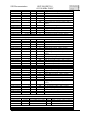
1
SIS Documentation
SIS3300/3301
65/100 MHz FADCs
SIS3300/SIS3301
65/100 MHz
VME FADCs
User Manual
SIS GmbH
Harksheider Str. 102A
22399 Hamburg
Germany
Phone: ++49 (0) 40 60 87 305 0
Fax:
++49 (0) 40 60 87 305 20
email: [email protected]
http://www.struck.de
Version: 3.00 as of 27.05.02
Page 1 of 64
SIS Documentation
SIS3300/SIS3301
65/100 MHz FADC
Revision Table:
Revision
0.01
1.00
1.01
1.02
1.03
1.10
Date
27.09.00
15.01.01
17.01.01
21.01.01
01.06.01
01.08.01
2.00
2.10
2.11
3.0x
29.10.01
05.11.01
15.11.01
24.05.02
3.00
27.05.02
Page 2 of 64
Modification
Generation
First official release
Trigger functionality added
MBLT64 readout
Bug fix in acquisition register
Documentation:
J190 description
Design Version 2 : (added Multiplexer Mode)
- Firmware Revision Register : 0x33000102
- new bit in Acquisition control register (bit 15; MULTIPLEXER
Mode)
- new Clock Predivider registers
- new No_of_Sample registers
- new Output 1 function in MULTIPLEXER Mode
V2 hardware revision, extended functionality
extended trigger functionality description
Bug fixes, ADC chip frequency range
Prerelease for major functionality/firmware upgrade V3
- implementation of gate chaining mode
- introduction of averaging
- 2e VME readout implementation
- change in trigger bit behaviour
Combination of SIS3300 and SIS3301 manual to one document
Official release
SIS Documentation
SIS3300/3301
65/100 MHz FADCs
- Table of contents
1
Table of contents ................................................................................................................. 3
Introduction ......................................................................................................................... 5
1.1
2
Related documents...................................................................................................................................5
Technical Properties/Features ............................................................................................. 6
2.1
Key functionality .....................................................................................................................................6
2.2
Module design .........................................................................................................................................7
2.2.1
Dual channel group..........................................................................................................................8
2.3
Modes of Operation .................................................................................................................................8
2.4
Memory management ..............................................................................................................................8
2.4.1
Single Event Mode...........................................................................................................................8
2.4.2
Multi Event Mode............................................................................................................................8
2.4.3
Dual Bank Mode..............................................................................................................................8
2.5
Clock sources...........................................................................................................................................9
2.5.1
Internal clock ...................................................................................................................................9
2.5.2
External clock ..................................................................................................................................9
2.5.3
Random External Clock...................................................................................................................9
2.6
Averaging ..............................................................................................................................................10
2.7
Trigger control (pre/post, start/stop and gate mode) ..............................................................................10
2.8
Internal Trigger generation ....................................................................................................................10
2.9
Time Stamp Memory .............................................................................................................................10
2.10 VME Interrupts......................................................................................................................................10
2.11 VME Readout Speed .............................................................................................................................11
3
VME Addressing............................................................................................................... 12
3.1
4
Address Map..........................................................................................................................................13
Register Description.......................................................................................................... 16
4.1
Control/Status Register(0x, write/read) .................................................................................................16
4.1.1
Trigger activation...........................................................................................................................17
4.1.2
Trigger routing...............................................................................................................................17
4.2
Module Id. and Firmware Revision Register (0x4, read).......................................................................18
4.2.1
Major revision numbers .................................................................................................................18
4.3
Interrupt configuration register (0x8) ....................................................................................................19
4.3.1
IRQ mode.......................................................................................................................................19
4.4
Interrupt control register (0xC)..............................................................................................................20
4.5
Acquisition control register (0x10, read/write)......................................................................................22
4.6
Start Delay register (0x14, read/write)...................................................................................................24
4.7
Stop Delay register (0x18, read/write)...................................................................................................24
4.8
Time stamp predivider register (0x1C)..................................................................................................25
4.9
Key address general reset (0x20, write).................................................................................................26
4.10 Key address VME start sampling (0x30, write).....................................................................................26
4.11 Key address VME stop sampling (0x34, write) .....................................................................................26
4.12 Key address start Auto Bank Switch mode (0x40, write) ......................................................................27
4.13 Key address stop Auto Bank Switch mode (0x44, write) ......................................................................27
4.14 Key address clear BANK1 FULL Flag (0x48, write) ...........................................................................27
4.15 Key address clear BANK2 FULL Flag (0x4C, write) ...........................................................................27
4.16 Event Time Stamp directory bank 1 (0x1000-0x1ffc, read only) ..........................................................28
4.17 Event Time Stamp directory bank 2 (0x2000-0x2ffc, read only) ..........................................................28
4.18 Event configuration registers (0x100000, 0x200000, 0x280000, 0x300000, 0x380000) .....................29
4.18.1
Gate chaining mode .......................................................................................................................30
4.18.2
Averaging mode.............................................................................................................................30
4.18.3
MULTIPLEXER MODE ...............................................................................................................30
4.18.4
EXTERNAL RANDOM CLOCK MODE ....................................................................................31
4.18.5
Page size ........................................................................................................................................31
4.19 Threshold registers (0x100004, 0x200004, 0x280004, 0x300004, 0x380004)......................................32
4.20 Trigger Flag Clear Counter register (0x10001C, 0x20001C, 0x28001C, 0x3001C, 0x38001C)..........34
4.21 Clock Predivider register (0x100020, 0x200020, 0x280020, 0x300020, 0x380020) ............................35
4.22 No_Of_Sample register (0x100024, 0x200024, 0x280024, 0x300024, 0x380024) ..............................36
Page 3 of 64
SIS Documentation
SIS3300/SIS3301
65/100 MHz FADC
4.23 Trigger setup register registers (0x100028, 0x200028, 0x280028, 0x300028, 0x380028)....................37
4.24 MAX No of Events registers (0x10002C, 0x20002C, 0x28002C, 0x30002C, 0x38002C) ...................38
4.25 Trigger event directory bank 1 (0x101000 – 0x101ffc).........................................................................39
4.26 Trigger event directory bank 2 (0x102000 – 0x102ffc).........................................................................39
4.27 Event directories bank 1 ( 0x201000 – 0x201ffc, 0x281000 – 0x281ffc,
0x301000 – 0x301ffc,
0x381000 – 0x381ffc)........................................................................................................................................40
4.28 Event directories bank 2 ( 0x202000 – 0x202ffc, 0x282000 – 0x282ffc,
0x302000 – 0x302ffc,
0x382000 – 0x382ffc)........................................................................................................................................40
4.29 Bank 1 address counter (0x200008, 0x280008, 0x300008, 0x380008).................................................41
4.30 Bank 2 address counter (0x20000C, 0x28000C, 0x30000C, 0x38000C) ..............................................41
4.31 Bank 1 event counter (0x200010, 0x280010, 0x300010, 0x380010) ....................................................42
4.32 Bank 2 event counter (0x200014, 0x280014, 0x300014, 0x380014) ....................................................42
4.33 Actual Sample registers (0x200018, 0x280018, 0x300018, 0x380018) ................................................43
4.34 Bank 1 memory (0x400000 – 0x5ffffc) ................................................................................................44
4.35 Bank 2 memory (0x600000 – 0x7ffffc) ................................................................................................44
5
Description of Start/Stop and Gate operation modi .......................................................... 45
5.1
Start/stop mode ......................................................................................................................................45
5.1.1
Front panel start/stop .....................................................................................................................45
5.2
Gate mode..............................................................................................................................................45
5.3
Start logic summary ...............................................................................................................................46
5.4
Stop logic summary ...............................................................................................................................47
6
Operation........................................................................................................................... 48
6.1
6.2
6.3
6.4
6.5
7
8
Configuration:........................................................................................................................................48
Arm for sampling:..................................................................................................................................48
Start Sampling: ......................................................................................................................................48
Stop Sampling (Event):..........................................................................................................................49
End of Sampling (clear arm / disable Sample Clock): ...........................................................................49
Board layout ...................................................................................................................... 50
Front panel......................................................................................................................... 51
8.1
Control In/Outputs .................................................................................................................................52
8.1.1
User input.......................................................................................................................................52
8.1.2
Control input termination...............................................................................................................52
8.2
Analog inputs.........................................................................................................................................52
8.2.1
Single ended LEMO version..........................................................................................................52
8.2.2
Differential version ........................................................................................................................52
8.3
LED's .....................................................................................................................................................53
8.4
PCB LEDs .............................................................................................................................................53
9
Jumpers/Configuration ...................................................................................................... 54
9.1
J1............................................................................................................................................................54
9.1.1
SIS3300_V1...................................................................................................................................54
9.1.2
SIS3300_V2 (and higher) ..............................................................................................................54
9.2
J190 Reset..............................................................................................................................................54
9.3
Offset adjustment...................................................................................................................................55
9.4
JTAG .....................................................................................................................................................56
10
Appendix........................................................................................................................ 57
10.1 Data acquisition modes..........................................................................................................................57
10.1.1 Multiplexer mode...........................................................................................................................57
10.1.2 Random external clock mode.........................................................................................................58
10.1.3
Auto bank switch mode .................................................................................................................58
10.2 consumption...........................................................................................................................................59
10.3 Operating conditions..............................................................................................................................59
10.3.1
Cooling ..........................................................................................................................................59
10.3.2 Hot swap/live insertion ..................................................................................................................59
10.4 Connector types .....................................................................................................................................60
10.5 P2 row A/C pin assignments..................................................................................................................60
10.6 Row d and z Pin Assignments ...............................................................................................................61
11
Index .............................................................................................................................. 62
Page 4 of 64
SIS Documentation
1
SIS3300/3301
65/100 MHz FADCs
Introduction
The SIS3300/3301 are eight channel ADC/digitizer boards with a sampling rate of up to 105
MHz (for the individual channel) and a resolution of 12/14-bit. The boards are single width
6U VME card, which has no special (i.e. non standard VME) voltage requirements.
Dual memory bank functionality in conjunction with multi event memory structure and a
range of trigger options give the unit the flexibility to cover a variety of applications.
Applications comprise but are not limited to:
• digitization of “slow” detectors like calorimeters
• spectroscopy with Ge-detecors
• beam profile monitor readout
• serialized readout of µ-Strip detector data
As we are aware, that no manual is perfect, we appreciate your feedback and will try to
incorporate proposed changes and corrections as quickly as possible. The most recent version
of this manual can be obtained by email from [email protected], the revision dates are online
under http://www.struck.de/manuals.htm.
1.1 Related documents
A list of available firmware designs can be retrieved from
http://www.struck.de/sis3300firm.htm
The JTAG firmware installation procedure is described in
http://www.struck.de/sis3300_jtagprog.pdf
Page 5 of 64
SIS Documentation
SIS3300/SIS3301
65/100 MHz FADC
2 Technical Properties/Features
2.1 Key functionality
Find below a list of key features of the SIS3300 and SIS3301 digitizers.
Sampling rate per channel
Minimum symmetric clock
Resolution
Analog bandwidth
Typical pedestal variance
Differential input version
2 x 128 KSample default
2 x 512 KSample option
(1)
(2)
SIS3300
105 MHz
1 MHz
12-bit
> 80 MHz
0.7 bit
X
-
SIS3301-65
65 MHz
15 MHz
14-bit
35 MHz (1)
1.1 bit (2)
X
X
X
SIS3301-105
105 MHz
15 MHz
14-bit
X
X
X
limited for better resolution
with symmetric input range
Common properties of all boards are:
•
•
•
•
•
•
•
•
•
•
•
•
•
•
•
•
•
•
•
•
8 channels
special clock modes (clock prescaling, external “arbitrary” clock)
channel to channel crosstalk below noise (i.e. invisible in Fourier spectrum)
external/internal clock
multi event mode
N sample averaging (N= 2,4, 8, ..., 128)
Read on the fly (actual sample value)
pre/post trigger option
Two independent memory banks
trigger generation
4 NIM control inputs/4 NIM control outputs
A32 D32/BLT32/MBLT64/2eVME
Geographical addressing mode (in conjunction with VME64x backplane)
Hot swap (in conjunction with VME64x backplane)
VME64x Connectors
VME64x Side Shielding
VME64x Front panel
VME64x extractor handles (on request)
F1002 compatible P2 row A/C assignment
+5 V, +12V and –12 V VME standard voltages
Note: The SIS3300/1 shall not be operated on P2 row A/C extensions, like VSB e.g. due to
the compatibility to the F1001 FADC modules clock and start/stop distribution scheme.
Page 6 of 64
SIS Documentation
SIS3300/3301
65/100 MHz FADCs
2.2 Module design
The SIS3300 consists of four identical groups of 2 ADC channels and a control section as
shown in the simplified block diagram below.
Front Panel
Control I/O
VME Interface
and
Control FPGA
VMEBus
System
Clock
Clock
Distribution
Dual Channel Group 4 (Channels 7 and 8)
Dual Channel Group 3 (Channels 5 and 6)
Dual Channel Group 2 (Channels 3 and 4)
Dual Channel Group 1 (Channels 1 and 2)
Page 7 of 64
SIS Documentation
SIS3300/SIS3301
65/100 MHz FADC
2.2.1 Dual channel group
Two ADC channels form a group, which memory is handled by one Field Programmable
Gate Array (FPGA).
32
12/14
Input
Stage 2
Data
ADC 2
Address
FPGA
Input
Stage 1
ADC 1
17
32
12/14
Event
Directory
Memory
Bank 2
Data
Address
Memory
Bank 1
17
2.3 Modes of Operation
The SIS3300 was developed with maximum flexibility in mind. The FPGA based design of
the card allows to meet the requirements of many readout applications with dedicated
firmware designs in the future. The initial firmware is supposed to furnish you with an easy to
use yet powerful high speed high resolution Flash Analog to Digital Converter (FADC)
implementation, that covers many everyday analog to digital applications.
2.4 Memory management
The individual memory bank(s) can be used either as one contiguous memory or as a
subdivided multi event memory. In addition memory depth can be limited in single event
operation to match the requirements of the given application. The memory configuration is
defined through the memory configuration register, while bank handling (on dual memory
bank modules) is under control of the acquisition control register.
2.4.1 Single Event Mode
The full memory of 128 K Samples of the SIS3300/1 is used as one big circular buffer or as
single shot memory in single event mode, unless memory size is limited by the event
configuration register.
2.4.2 Multi Event Mode
The memory can be divided in up to 1024 pages or events to make the acquisition of shorter
signals more efficient. The stop pointers for the individual page can be retrieved from the
event directory. In auto start mode the ADC advances to the next page and starts sampling
automatically.
2.4.3 Dual Bank Mode
Dual bank mode (Bank Switch mode) is available on cards (except SIS3300 V1 PCBs). The
single/multi event selection will influence both memory banks in the same fashion. Data from
the inactive bank can be readout, while the other bank is acquiring new data.
Page 8 of 64
SIS Documentation
SIS3300/3301
65/100 MHz FADCs
2.5 Clock sources
The SIS3300/3301 features 3 basic clock modes
• Internal clock
• External symmetric clock
• External random clock
2.5.1 Internal clock
The internal clock is generated from an on board 50 MHz quartz. It is either doubled by a
delay locked loop to 100 MHz or divided down to lower clock frequencies. The table below
lists the valid clock settings for the different SIS3300/3301 boards.
Clock
100 MHz
50 MHz
25 MHz
12.5 MHz
6.25 MHz
3.125 MHz
SIS3300
X
X
X
X
X
X
SIS3301-65
X
X
-
SIS3301-105
X
X
X
-
2.5.2 External clock
A symmetric external clock (NIM level, ratio between 45:55 and 55:45) can be fed to the
module through a LEMO00 connector. An ECL clock over rows A/C of the J2 VME
backplane can be used as an alternative. For optimum performance the clock frequency
should be within the specified range for the given ADC chip.
Module
SIS3300
SIS3301-65
SIS3301-105
Min. sym. clock
1 MHz
15 MHz
15 MHz
Max sym. clock
105 MHz
65 MHz
105 MHz
2.5.3 Random External Clock
Random external clock mode allows to operate the SIS3300/1 with basically arbitrary external
clock pulse trains or slow external clocks. The module is clocked with the internal clock
(typically at 100 MHz) and a data word will be stored to memory upon the next leading edge
of the internal clock after a leading edge on the external clock input is detected. Internal
pipelining has to be taken into account, the datum will precede the clock by 10 clock ticks
(i.e. about 100 ns on a SIS3300 clocking at 100 MHz).
Page 9 of 64
SIS Documentation
SIS3300/SIS3301
65/100 MHz FADC
2.6 Averaging
Averaging over N (N=2, 4, 8, ..., 128) consecutive samples can be used to cover the domain
of lower speed digitizers with the SIS3300/1 cards without compromising on the
resolution/signal to noise ratio side.
2.7
Trigger control (pre/post, start/stop and gate mode)
The SIS3300/1 features pre/post trigger capability as well as start/stop mode acquisition and a
gate mode (in which start and stop are derived from the leading and trailing edge of a single
control input signal).
The trigger behaviour is defined by the acquisition control register.
2.8
Internal Trigger generation
The trigger output of the SIS3300/1 can be either used to interact with external trigger logic or
to base start/stop on a threshold (i.e. one individual threshold per ADC channel) of the
digitized data. Trigger generation can be activated with two conditions:
• module armed (i.e. sample clock active, trigger can be used to start acquisition)
• module armed and started (trigger can be used to stop acquisition)
The user can select between triggering on the conditions above and below threshold
2.9 Time Stamp Memory
A 1024 x 24 bit Time Stamp Memory is implemented for each memory bank.
An internal counter starts with the first Stop trigger condition in multievent mode and it will
be incremented with the sample clock or with the predivided sample clock (factor 1 to 256).
Each stop trigger condition (end of event) writes the counter value into Time Stamp Memory.
2.10 VME Interrupts
Two registers, the Interrupt configuration and the Interrupt control register, are implemented
for interrupt setup and control.
Four Interrupt sources are implemented:
- External User Input (LEMO input 1)
- End of event
- End of last event in multievent mode
- Memory bank full in bank switch mode (Dual bank)
Page 10 of 64
SIS Documentation
SIS3300/3301
65/100 MHz FADCs
2.11 VME Readout Speed
The VME interface is optimized for readout speed. An internal FIFO/pipeline structure allows
for high speed readout in block transfer mode (BLT32, MBLT64, 2eVME).
The timings below were measured with the SIS3100 (VME master) and the SIS3300/SIS3301
(VME Slave). The upper scope trace shows the VME signal DS1* (Data strobe, low active).
The VME Master asserts the DS1* to request (read) data.
The lower signal shows the VME signal DTACK* (Data Acknowledge, low active). The
VME Slave asserts the DTACK* to acknowledge. that the data is valid on VME.
SIS330x DS* to DTACK* : 30-40ns
32bit every 120ns
-- > ~ 33 MByte/sec
BLT32
SIS330x DS* to DTACK* : 30-40ns
64bit every 125ns
-- > ~ 64 MByte/sec
MBLT64
SIS330x DS* to DTACK* : 50-60ns
128bit every 200ns
--> ~ 80 MByte/sec
2eVME
Page 11 of 64
SIS Documentation
SIS3300/SIS3301
65/100 MHz FADC
3 VME Addressing
As the SIS3300 VME FADC features memory options with up to 2 banks of 4 times 128 K
samples each, A32 addressing was implemented as the only option. Hence the module
occupies an address space of 0xFFFFFF Bytes (i.e. 16 MBytes) are used by the module.
The SIS3300/1 firmware addressing concept is a pragmatic approach to combine standard
rotary switch style settings with the use of VME64x backplane geographical addressing
functionality.
The base address is defined by the selected addressing mode, which is defined by jumper
array J1 and possibly SW1 and SW2 (in non geographical mode).
J1
Function
EN_A32
EN_GEO
EN_VIPA
reserved
The table below summarises the possible base address settings.
x
Shorthand
SW1/SW2
GA0-GA4
GA0
GA1
GA2
GA3
GA4
0
x
0
x
0
J1 Setting
Bits
A32 GEO VIPA 31 30 29 28 27 26 25 24
x
SW1
SW2
Not implemented in this design
Explanation
Setting of rotary switch SW1 or SW2 respective
Geographical address bit as defined by the VME64x(P) backplane
Notes:
• This concept allows the use of the SIS3300/1 in standard VME as well as in VME64x
environments, i.e. the user does not need to use a VME64x backplane.
• The factory default setting is EN_A32 closed, SW1=3, SW2=0 (i.e. the module will react
to A32 addressing under address 0x30000000)
• Early SIS3300 boards (PCB SIS3300_V1) have a different base address scheme
Page 12 of 64
SIS Documentation
SIS3300/3301
65/100 MHz FADCs
3.1 Address Map
The SIS3300 resources and their locations are listed in the table below.
Note: Write access to a key address (KA)with arbitrary data invokes the respective action
Offset
Size in
Bytes
BLT
Access
-
W/R
R
R/W
R/W
R/W
BLT32
BLT32
R/W
R/W
R/W
KA W
KA W
KA W
KA W
KA W
KA W
KA W
R
R
Control/Status Register (J-K register)
Module Id. and Firmware Revision register
Interrupt configuration register
Interrupt control register
Acquisition control/status register (J-K
register)
Extern Start Delay register
Extern Stop Delay register
Time stamp predivider register
General Reset
VME Start sampling
VME Stop sampling
Start auto bank switch
Stop auto bank switch
Clear bank 1 memory full
Clear bank 2 memory full
Event Time Stamp directory bank 1
Event Time Stamp directory bank 2
Event information all ADC groups
0x00100000
4
0x00100004
4
0x0010001C
4
0x00100020
4
0x00100024
4
0x00100028
4
0x0010002C
4
0x00101000
0x1000 BLT32
0x00102000
0x1000 BLT32
W only
W only
W only
W only
W only
W only
W only
R
R
Event configuration register (all ADCs)
Trigger Threshold register (all ADCs)
Trigger Flag Clear Counter register (all ADCs)
Clock Predivider register (all ADCs)
No_Of_Sample register (all ADCs)
Trigger setup register (all ADCs)
Max. No of Events register (all ADCs)
Event directory bank 1 (all ADCs)
Eevent directory bank 2 (all ADCs)
0x00000000
0x00000004
0x00000008
0x0000000C
0x00000010
4
4
4
4
4
0x00000014
0x00000018
0x0000001C
0x00000020
0x00000030
0x00000034
0x00000040
0x00000044
0x00000048
0x0000004C
0x00001000
0x00002000
4
4
4
4
4
4
4
4
4
4
0x1000
0x1000
Event information ADC group 1
0x00200000
4
0x00200004
4
0x00200008
4
0x0020000C
4
0x00200010
4
0x00200014
4
0x00200018
4
0x0020001C
4
0x00200020
0x00200024
0x00200028
0x0020002C
0x00201000
0x00202000
4
4
4
4
0x1000
0x1000
Event information ADC group 2
0x00280000
4
-
R/W
R/W
R
R
R
R
R
R/W
BLT32
BLT32
R/W
R/W
R/W
R/W
R
R
-
R/W
Function
Event configuration register (ADC1, ADC2)
Trigger Threshold register (ADC1, ADC2)
Bank1 address counter (ADC1, ADC2)
Bank2 address counter (ADC1, ADC2)
Bank1 Event counter (ADC1, ADC2)
Bank2 Event counter (ADC1, ADC2)
Actual Sample Value (ADC1, ADC2)
Trigger Flag Clear Counter register (ADC1,
ADC2)
Clock Predivider register (ADC1, ADC2)
No_Of_Sample register (ADC1, ADC2)
Trigger setup register (ADC1, ADC2)
Max. No of Events register (ADC1, ADC2)
Event directory bank 1 (ADC1, ADC2)
Event directory bank 2 (ADC1, ADC2)
Event configuration register (ADC3, ADC4)
Page 13 of 64
SIS Documentation
SIS3300/SIS3301
65/100 MHz FADC
0x00280004
0x00280008
0x0028000C
0x00280010
0x00280014
0x00280018
0x0028001C
4
4
4
4
4
4
4
0x00280020
0x00280024
0x00280028
0x0028002C
0x00281000
0x00282000
4
4
4
4
0x1000
0x1000
Event information ADC group 3
0x00300000
4
0x00300004
4
0x00300008
4
0x0030000C
4
0x00300010
4
0x00300014
4
0x00300018
4
0x0030001C
4
0x00300020
0x00300024
0x00300028
0x0030002C
0x00301000
0x00302000
4
4
4
4
0x1000
0x1000
Event information ADC group 4
0x00380000
4
0x00380004
4
0x00380008
4
0x0038000C
4
0x00380010
4
0x00380014
4
0x00380018
4
0x0038001C
4
0x00380020
0x00380024
0x00380028
0x0038002C
0x00381000
0x00382000
Bank 1 memory
0x00400000
0x00480000
0x00500000
0x00580000
Bank 2 memory
Page 14 of 64
4
4
4
4
0x1000
0x1000
0x80000
0x80000
0x80000
0x80000
-
BLT32
BLT32
-
BLT32
BLT32
-
BLT32
BLT32
R/W
R
R
R
R
R
R/W
R/W
R/W
R/W
R/W
R
R
R/W
R/W
R
R
R
R
R
R/W
R/W
R/W
R/W
R/W
R
R
R/W
R/W
R
R
R
R
R
R/W
R/W
R/W
R/W
R/W
R
R
Trigger Threshold register (ADC3, ADC4)
Bank1 address counter (ADC3, ADC4)
Bank2 address counter (ADC3, ADC4)
Bank1 Event counter (ADC3, ADC4)
Bank2 Event counter (ADC3, ADC4)
Actual Sample Value (ADC1, ADC2)
Trigger Flag Clear Counter register (ADC1,
ADC2)
Clock Predivider register (ADC3, ADC4)
No_Of_Sample register (ADC3, ADC4)
Trigger setup register (ADC3, ADC4)
Max. No of Events register (ADC3, ADC4)
Event directory bank 1 (ADC3, ADC4)
Event directory bank 2 (ADC3, ADC4)
Event configuration register (ADC5, ADC6)
Trigger Threshold register (ADC5, ADC6)
Bank1 address counter (ADC5, ADC6)
Bank2 address counter (ADC5, ADC6)
Bank1 Event counter (ADC5, ADC6)
Bank2 Event counter (ADC5, ADC6)
Actual Sample Value (ADC1, ADC2)
Trigger Flag Clear Counter register (ADC1,
ADC2)
Clock Predivider register (ADC5, ADC6)
No_Of_Sample register (ADC5, ADC6)
Trigger setup register (ADC5, ADC6)
Max. No of Events register (ADC5, ADC6)
Event directory bank 1 (ADC5, ADC6)
Event directory bank 2 (ADC5, ADC6)
Event configuration Register (ADC7, ADC8)
Trigger Threshold register (ADC7, ADC8)
Bank1 address counter (ADC7, ADC8)
Bank2 address counter (ADC7, ADC8)
Bank1 Event counter (ADC7, ADC8)
Bank2 Event counter (ADC7, ADC8)
Actual Sample Value (ADC7, ADC8)
Trigger Flag Clear Counter register (ADC1,
ADC2)
Clock Predivider register (ADC7, ADC8)
No_Of_Sample register (ADC7, ADC8)
Trigger setup register (ADC7, ADC8)
Max. No of Events register (ADC7, ADC8)
Event directory bank 1 (ADC7, ADC8)
Event directory bank 2 (ADC7, ADC8)
BLT32/MBLT64/2eVME
BLT32/MBLT64/2eVME
BLT32/MBLT64/2eVME
BLT32/MBLT64/2eVME
R/W*
R/W*
R/W*
R/W*
Bank 1 memory (ADC1, ADC2)
Bank 1 memory (ADC3, ADC4)
Bank 1 memory (ADC5, ADC6)
Bank 1 memory (ADC7, ADC8)
SIS Documentation
0x00600000
0x00680000
0x00700000
0x00780000
0x80000
0x80000
0x80000
0x80000
SIS3300/3301
65/100 MHz FADCs
BLT32/MBLT64/2eVME
BLT32/MBLT64/2eVME
BLT32/MBLT64/2eVME
BLT32/MBLT64/2eVME
R/W*
R/W*
R/W*
R/W*
Bank 2 memory (ADC1, ADC2)
Bank 2 memory (ADC3, ADC4)
Bank 2 memory (ADC5, ADC6)
Bank 2 memory (ADC7, ADC8)
*
W in D32 only (for memory test e.g.)
Note 1: The event information is identical for the four ADC groups (unless the module has a
hardware problem), hence it will be sufficient for normal operation to retrieve the needed
information from one group only.
Note 2: MBLT64 and 2eVME read access is supported from the memory banks only.
Page 15 of 64
SIS Documentation
SIS3300/SIS3301
65/100 MHz FADC
4 Register Description
The function of the individual registers is described in detail in this section.
The first line after the subsection header (in Courier font) like:
#define SIS3300_CONTROL_STATUS
0x0
/* read/write; D32 */
refers to the sis3300.h header file.
4.1
Control/Status Register(0x, write/read)
#define SIS3300_CONTROL_STATUS
0x0
/* read/write; D32 */
The control register is in charge of the control of basic properties of the SIS3300/1 board, like
output signal assignment, in write access. It is implemented via a selective J/K register, a
specific function is enabled by writing a 1 into the set/enable bit, the function is disabled by
writing a 1 into the clear/disable bit (which location is 16-bit higher in the register). An
undefined toggle status will result from setting both the enable and disable bits for a specific
function at the same time.
On read access the same register represents the status register.
Bit
31
30
29
28
27
26
25
24
23
22
21
20
19
18
17
16
15
14
13
12
11
10
9
8
write Function
Clear reserved 15 (*)
Clear reserved 14 (*)
Clear reserved 13 (*)
Clear reserved 12 (*)
Clear reserved 11 (*)
clear bank full pulse to output 3 (*)
clear bank full pulse to output 2 (*)
clear bank full pulse to output 1 (*)
Clear reserved 7 (*)
Disable internal trigger routing (*)
Activate trigger upon armed (*)
Non inverted trigger output (*)
Clear reserved 3 (*)
Enable user output/disable trigger output (*)
Clear user output (*)
Switch off user LED (*)
Set reserved 15
Set reserved 14
Set reserved 13
Set reserved 12
Set reserved 11
set bank full pulse to output 3
set bank full pulse to output 2
set bank full pulse to output 1
7
6
Set reserved 7
Enable internal trigger routing
5
Activate trigger upon armed and started
4
Invert trigger output
3
Set reserved 3
Page 16 of 64
read Function
Status P2_SAMPLE_IN
Status P2_RESET_IN
Status P2_TEST_IN
Status User Input
Status Control 15
Status Control 14
Status Control 13
Status Control 12
Status Control 11
Status Bank full pulse on LEMO output 3
Status Bank full pulse on LEMO output 2
Status Bank full pulse on LEMO output 1
(highest priority)
Status Control 7
Status trigger routing (1=
to input, 0=don’t route)
Status trigger generation (1=armed and
started, 0=armed)
Status trigger output inversion(1=inverted,
0=straight)
Status Control 3
SIS Documentation
SIS3300/3301
65/100 MHz FADCs
2
Enable trigger output/disable user output
1
Set user output (if bit 2 is not set)
0
Switch on user LED
multiplexer mode = 0:
Status of user/trigger output (1=trigger
output, 0=user output)
multiplexer mode = 1:
output set by multiplexer out pulse
Status User Output (1=output on, 0=output
off)
Status User LED (1=LED on, 0=LED off)
(*) denotes power up default setting
4.1.1 Trigger activation
Trigger generation can be activated for two states of the SIS3300/1. By default trigger
generation is active as soon as the module is armed (i.e. a sample clock is active). In this
mode the trigger can be used to start the digitizer (with stop condition end of event e.g.).
Trigger generation upon armed and started (i.e. bit 6 of the control register set), the trigger is
used to stop the module (what is a efficient mode of operation in conjunction with autostart
e.g.).
4.1.2 Trigger routing
The trigger status is present on LEMO output 1 (with user output and multiplexer mode
disabled). It can be used to form a general trigger decision with external trigger electronics,
which is fed back to the corresponding input (start/stop) on the digitizer(s). The trigger is
routed on board to the stop input with the internal trigger routing bit set.
Page 17 of 64
SIS Documentation
4.2
SIS3300/SIS3301
65/100 MHz FADC
Module Id. and Firmware Revision Register (0x4, read)
#define SIS3300_MODID
0x4
/* read only; D32 */
This register reflects the module identification of the SIS3300/1 and its minor and major
firmware revision levels. The major revision level will be used to distinguish between
substantial design differences and experiment specific designs, while the minor revision level
will be used to mark user specific adaptations.
Bit
31
30
29
28
27
26
25
24
23
22
21
20
19
18
17
16
15
14
13
12
11
10
9
8
7
6
5
4
3
2
1
0
Function
Module Id. Bit 15
Module Id. Bit 14
Module Id. Bit 13
Module Id. Bit 12
Module Id. Bit 11
Module Id. Bit 10
Module Id. Bit 9
Module Id. Bit 8
Module Id. Bit 7
Module Id. Bit 6
Module Id. Bit 5
Module Id. Bit 4
Module Id. Bit 3
Module Id. Bit 2
Module Id. Bit 1
Module Id. Bit 0
Major Revision Bit 7
Major Revision Bit 6
Major Revision Bit 5
Major Revision Bit 4
Major Revision Bit 3
Major Revision Bit 2
Major Revision Bit 1
Major Revision Bit 0
Minor Revision Bit 7
Minor Revision Bit 6
Minor Revision Bit 5
Minor Revision Bit 4
Minor Revision Bit 3
Minor Revision Bit 2
Minor Revision Bit 1
Minor Revision Bit 0
Reading
4.2.1 Major revision numbers
Find below a table with major revision numbers used to date
Major revision number
0x01 to 0x0F
0x10
Page 18 of 64
Application/user
Generic designs
Amanda
3
3
0
0/1
SIS Documentation
4.3
SIS3300/3301
65/100 MHz FADCs
Interrupt configuration register (0x8)
#define SIS3300_IRQ_CONFIG
0x8
/* read/write; D32 */
This read/write register controls the VME interrupt behaviour of the SIS3300 ADC. Four
interrupt sources are foreseen, for the time being three of them are associated with an interrupt
condition, the fourth condition is reserved for future use.
The interrupter type is DO8 .
4.3.1 IRQ mode
In RORA (release on register access) mode the interrupt will be pending until the IRQ
source is cleared by specific access to the corresponding disable VME IRQ source bit. After
the interrupt is serviced the source has to be activated with the enable VME IRQ source bit
again.
In ROAK (release on acknowledge) mode , the interrupt condition will be cleared (and the
IRQ source disabled) as soon as the interrupt is acknowledged by the CPU. After the interrupt
is serviced the source has to be activated with the enable VME IRQ source bit again. ROAK
IRQ mode can be used in conjunction with the University of Bonn LINUX Tundra Universe
II driver by Dr. Jürgen Hannappel on Intel based VME SBCs.
Bit
31
...
16
15
14
13
12
11
10
9
8
7
6
5
4
3
2
1
0
Function
RORA/ROAK Mode (0: RORA; 1: ROAK)
VME IRQ Enable (0=IRQ disabled, 1=IRQ enabled)
VME IRQ Level Bit 2
VME IRQ Level Bit 1
VME IRQ Level Bit 0
IRQ Vector Bit 7; placed on D7 during VME IRQ ACK cycle
IRQ Vector Bit 6; placed on D6 during VME IRQ ACK cycle
IRQ Vector Bit 5; placed on D5 during VME IRQ ACK cycle
IRQ Vector Bit 4; placed on D4 during VME IRQ ACK cycle
IRQ Vector Bit 3; placed on D3 during VME IRQ ACK cycle
IRQ Vector Bit 2; placed on D2 during VME IRQ ACK cycle
IRQ Vector Bit 1; placed on D1 during VME IRQ ACK cycle
IRQ Vector Bit 0; placed on D0 during VME IRQ ACK cycle
Default
0
0
0
0
0
0
0
0
0
0
0
0
0
0
0
0
0
0
0
The power up default value reads 0x 00000000
Page 19 of 64
SIS Documentation
4.4
SIS3300/SIS3301
65/100 MHz FADC
Interrupt control register (0xC)
#define SIS3300_IRQ_CONTROL
0xC
/* read/write; D32 */
This register controls the VME interrupt behaviour of the SIS3300 ADC. Four interrupt
sources are foreseen, for the time being three of them are associated with an interrupt
condition, the fourth condition is reserved for future use.
Bit
31
30
29
28
27
26
25
24
23
22
21
20
19
18
17
16
15
14
13
12
11
...
4
3
2
1
0
Function (w)
unused
unused
unused
unused
unused
unused
unused
unused
Clear IRQ source 3
Clear IRQ source 2
Clear IRQ source 1
Clear IRQ source 0
Disable IRQ source 3
Disable IRQ source 2
Disable IRQ source 1
Disable IRQ source 0
unused
unused
unused
unused
unused
...
unused
Enable IRQ source 3
Enable IRQ source 2
Enable IRQ source 1
Enable IRQ source 0
(r)
Status IRQ source 3 (user input)
Status IRQ source 2 (reserved)
Status IRQ source 1 (end of last event, bank full)
Status IRQ source 0 (end of event)
Status VME IRQ
Status internal IRQ
0
0
Status flag source 3
Status flag source 2
Status flag source 1
Status flag source 0
0
0
0
0
0
0
0
0
0
...
0
Status enable source 3 (read as 1 if enabled, 0 if disabled)
Status enable source 2 (read as 1 if enabled, 0 if disabled)
Status enable source 1 (read as 1 if enabled, 0 if disabled)
Status enable source 0 (read as 1 if enabled, 0 if disabled)
The power up default value reads 0x 00000000
Page 20 of 64
Default
0
0
0
0
0
0
0
0
0
0
0
0
0
0
0
0
0
0
0
0
0
0
0
0
0
0
0
SIS Documentation
SIS3300/3301
65/100 MHz FADCs
The generation of the status flags, the IRQ flags and the actual IRQ is illustrated with the
schematic below:
Status FLAG
Source 0
Source 0
Clear
Source 1
Source 2
Clear
AND
Status IRQ
Source 1
Enable 1
Status FLAG
Source 2
AND
VME_IRQ
internal
VME_IRQ
OR
Clear
Status IRQ
Source 2
Enable 2
Status FLAG
Source 3
Source 3
Clear
Status IRQ
Source 0
Enable 0
Status FLAG
Source 1
Clear
AND
AND
Status IRQ
Source 3
Enable 3
VME_IRQ_ENABLE
ROAK
AND
RD_IRQ_ACK
Page 21 of 64
SIS Documentation
4.5
SIS3300/SIS3301
65/100 MHz FADC
Acquisition control register (0x10, read/write)
#define SIS3300_ACQUISTION_CONTROL
0x10
/* read/write; D32 */
The acquisition control register is in charge of most of the settings related to the actual
configuration of the digitization process.
Like the control register it is implemented in a J/K fashion.
Bit
31
30
29
28
27
26
25
24
23
22
21
20
19
18
17
16
15
14
13
12
11
10
9
8
7
6
5
4
3
2
1
0
Write Function
Clear multiplexer mode
Clear Clock Source Bit2
Clear Clock Source Bit1
Clear Clock Source Bit0
Disable external clock random mode
Disable front panel gate mode (not start/stop)
Disable P2 Start/Stop logic
Disable front panel LEMO start/stop logic
Disable external stop delay
Disable external start delay
Disable multi event mode
0 : Enable sample clock will be cleared with end of event
1 : Enable sample clock will be cleared at end of bank only
(i.e. with last page of memory)
Disable Autostart (in multi event mode only )
Disable reserved
Disable auto bank switch mode
Disable sample clock for memory bank 2 (disarm sampling)
Disable sample clock for memory bank 1 (disarm sampling)
Set multiplexer mode
Set clock source Bit 2
Set clock source Bit 1
Set clock source Bit 0
Enable external clock random mode
Enable front panel gate mode (not Start/Stop)
Enable P2 Start/Stop logic
Enable front panel Lemo Start/Stop logic
Enable stop delay (value defined by stop delay register)
Enable start delay (value defined by start delay register)
Enable multi event mode
0 : Enable Sample Clock will be cleared with end of event
1 : Enable Sample Clock will be cleared at end of bank only
(i.e. with last page of memory)
Enable Autostart (in multi event mode only )
Enable reserved
Enable auto bank switch mode
Enable Sample Clock for Memory Bank 2 (arm for sampling)
Enable Sample Clock for Memory Bank 1 (arm for sampling)
The power up default value reads 0x
Page 22 of 64
Read
0
0
0
0
0
0
0
0
Bank 2 full
Bank 2 busy
Bank 1 full
Bank 1 busy
0
Bank switch busy
0
ADC_BUSY
Status multiplexer mode
Status clock source Bit 2
Status clock source Bit 1
Status clock source Bit 0
Status external clock random mode
Status front panel gate mode
Status P2 start/stop logic
Status front panel start/stop logic
Status stop delay
Status start delay
Status multi event mode
Status Autostart
Status reserved
Status auto bank switch mode
Status sample clock bank 2
Status sample clock bank 1
SIS Documentation
SIS3300/3301
65/100 MHz FADCs
Clock source bit setting table:
Clock Source
Bit2
0
0
0
0
1
1
1
1
Clock Source
Bit1
0
0
1
1
0
0
1
1
Clock Source
Bit0
0
1
0
1
0
1
0
1
Clock Source
internal 100 MHz
internal 50 MHz
internal 25 MHz
internal 12.5 MHz
internal 6.25 MHz
internal 3.125 MHz
external clock (front panel)
P2-Clock
Refer to the table in section 2.5.2for allowed clock speeds. Lower sampling rates into memory
can be accomplished with a sampling clock within the specified range in combination with the
clock predivider register in multiplexer mode or random external clock mode.
Page 23 of 64
SIS Documentation
4.6
SIS3300/SIS3301
65/100 MHz FADC
Start Delay register (0x14, read/write)
#define SIS3300_START_DELAY
0x14
/* read/write; D32 */
Pretrigger operation can be implemented via the start delay register in conjunction with front
panel start/stop or gate mode operation. The external and autostart start signal (or leading
edge of the gate) will be delayed by the value of the register+2 clocks if the external start
delay is enabled in the acquisition control register.
Bit
32
...
16
15
..
..
0
unused, read as 0
unused, read as 0
START_DELAY_BIT15
START_DELAY_BIT0
The power up default value is 0
4.7
Stop Delay register (0x18, read/write)
#define SIS3300_STOP_DELAY
0x18
/* read/write; D32 */
Posttrigger operation can be implemented via the stop delay register in conjunction with front
panel start/stop or gate mode operation. The external stop signal (or trailing edge of the gate)
will be delayed by the value of the register+2 clocks if the stop delay is enabled in the
acquisition control register.
Bit
32
...
16
15
..
..
0
unused, read as 0
unused, read as 0
STOP_DELAY_BIT15
STOP _DELAY_BIT0
The power up default value is 0
Page 24 of 64
SIS Documentation
SIS3300/3301
65/100 MHz FADCs
Note: The user can generate a gate of defined length (in clock ticks) by fanning a short pulse
to the start and stop input with start/stop mode active, stop delay enabled and the stop delay
register programmed to the desired gate width. Pipelining will have to be taken into account,
i.e. the digitised signal is about 40 ns (with the module sampling at 100 MHz) ahead of the
respective control signal, a fact that can be used in external trigger decisions.
For longer external trigger decisions one can consider to pipeline the ADC data in the FPGA
in future firmware revisions before storing them to memory.
4.8
Time stamp predivider register (0x1C)
#define SIS3300_TIMESTAMP_PREDIVIDER
0x1C
/* read/write; D32 */
The (read/write) time stamp predivider register is used to define a prescale factor for the
frequency of the time stamp counter. The time stamp counter counts at the clock rate with the
time stamp predivider value of 0 and 1, a prescale factor of 2 ... 65535 is selected by writing
the corresponding value to the register.
Bit
31
...
16
15
..
..
0
unused, read as 0
unused, read as 0
Time stamp predivider BIT15
Time stamp predivider BIT0
The power up default value is 0
Note: A predivider value of 0 can not be used with firmware V201
Page 25 of 64
SIS Documentation
4.9
SIS3300/SIS3301
65/100 MHz FADC
Key address general reset (0x20, write)
#define SIS3300_KEY_RESET
0x20
/* write only; D32 */
A write with arbitrary data to this register (key address) resets the SIS3300 to it’s power up
state.
4.10 Key address VME start sampling (0x30, write)
#define SIS3300_KEY_START
0x30
/* write only; D32 */
A write with arbitrary data to this register (key address) will initiate sampling on the active
memory bank if a bank is armed for sampling.
4.11 Key address VME stop sampling (0x34, write)
#define SIS3300_KEY_STOP
0x34
/* write only; D32 */
A write with arbitrary data to this register (key address) will halt sampling on the active page.
In Single Event Mode or during the last page the sampling this command will halt the the
sampling.
To Abort a sampling in Multi Event / Multibank mode the following cycles have to be
executed:
- issue “disable autostart” / issue KEY_STOP_AUTO_BANK_SWITCH
- issue SIS3300_KEY_STOP
- issue clear BX_ENABLE
Page 26 of 64
SIS Documentation
SIS3300/3301
65/100 MHz FADCs
4.12 Key address start Auto Bank Switch mode (0x40, write)
#define SIS3300_KEY_START_AUTO_BANK_SWITCH 0x40
/* write only; D32 */
A write with arbitrary data to this register (key address) will start the auto bank switch mode.
4.13 Key address stop Auto Bank Switch mode (0x44, write)
#define SIS3300_KEY_STOP_AUTO_BANK_SWITCH
0x44
/* write only; D32 */
A write with arbitrary data to this register (key address) will stop the auto bank switch mode.
4.14 Key address clear BANK1 FULL Flag (0x48, write)
#define SIS3300_KEY_BANK1_FULL_FLAG
0x48
/* write only; D32 */
A write with arbitrary data to this register (key address) will clear the BANK1 FULL Flag.
4.15 Key address clear BANK2 FULL Flag (0x4C, write)
#define SIS3300_KEY_BANK2_FULL_FLAG
0x4C
/* write only; D32 */
A write with arbitrary data to this register (key address) will clear the BANK2 FULL Flag.
Page 27 of 64
SIS Documentation
SIS3300/SIS3301
65/100 MHz FADC
4.16 Event Time Stamp directory bank 1 (0x1000-0x1ffc, read only)
#define SIS3300_EVENT_TIMESTAMP_DIR_BANK1
0x1000
/* read only; D32, BLT32; size: 0x1000 */
The event time stamp directory can be used to measure time between triggers (stops) in multi
event mode. A scaler counting the ADC clock is enabled with the first stop (hence the time
stamp for the first event will read 0 always). The counter value (of the 24-bit wide) scaler is
written to the corresponding location for subsequent events.
offset address
0x0
..
0xffc
Time Stamp (D23:D0)
Time Stamp 0
Time Stamp 1023
4.17 Event Time Stamp directory bank 2 (0x2000-0x2ffc, read only)
#define SIS3300_EVENT_TIMESTAMP_DIR_BANK2
0x2000
/* read only; D32, BLT32; size: 0x1000 */
As for bank 1.
offset address
0x0
..
0xffc
Page 28 of 64
Time Stamp (D23:D0)
Time Stamp 0
Time Stamp 1023
SIS Documentation
SIS3300/3301
65/100 MHz FADCs
4.18 Event configuration registers (0x100000, 0x200000, 0x280000, 0x300000, 0x380000)
#define SIS3300_EVENT_CONFIG_ALL_ADC
0x100000
/* write only;D32 */
#define
#define
#define
#define
SIS3300_EVENT_CONFIG_ADC12
SIS3300_EVENT_CONFIG_ADC34
SIS3300_EVENT_CONFIG_ADC56
SIS3300_EVENT_CONFIG_ADC78
0x200000
0x280000
0x300000
0x380000
/*
/*
/*
/*
read/write;D32
read/write;D32
read/write;D32
read/write;D32
*/
*/
*/
*/
This register is implemented for each channel group and it has to be written with the same
value, the best way is to make use of the address SIS3300_EVENT_CONFIG_ALL_ADC to write
to the registers of all channel groups simultaneously.
The number of memory divisions (events) is defined by this register in multi event mode. The
lowest three bits define the number of memory divisions as listed in the table below. On dual
bank units both memory banks will be affected by the configuration of the event configuration
register. The maximum number of events is defined by the size of the event directory, which
has 1024 entries. The maximum number of events is limited to 65535 in gate chaining mode
to allow for shorter gates also.
.
Bit
31
...
20
19
18
17
16
15
14
13
12
11
10
9
8
7
6
5
4
3
2
1
0
function
unused; read 0
...
unused; read 0
Event_CONF Bit 19 (reserved function)
Average Bit 2
Average Bit 1
Average Bit 0
MULTIPLEXER MODE
Event_CONF Bit 14 (reserved function)
Event_CONF Bit 13 (reserved function)
1 (former enable trigger event directory)
EXTERNAL CLOCK RANDOM MODE
Event_CONF Bit 10 (reserved function)
Channel Group ID Bit 1
Channel Group ID Bit 0
Event_CONF Bit 7 (reserved function)
Event_CONF Bit 6 (reserved function)
Event_CONF Bit 5 (reserved function)
ENABLE_GATE_CHAINING_MODE
Enable Wrap around mode (no address auto stop)
0 : Autostop at end of page
1 : Wrap around page until STOP (External or KEY)
Page size Bit 2
Page size Bit 1
Page size Bit 0
Page 29 of 64
SIS Documentation
SIS3300/SIS3301
65/100 MHz FADC
The power up default values of the registers are
SIS3300_EVENT_CONFIG_ADC12:
SIS3300_EVENT_CONFIG_ADC34:
SIS3300_EVENT_CONFIG_ADC56:
SIS3300_EVENT_CONFIG_ADC78:
0x00001000
0x00001100
0x00001200
0x00001300
(i.e. the two channel group ID bits identify the four channel groups)
4.18.1 Gate chaining mode
Gate chaining mode was implemented to allow for effective acquisition of small events of
arbitrary length.
Sampling in gate chaining mode will stop when:
• Maximum number of events (see 4.24 ) is reached
• End of bank is reached, the last event/gate may be incomplete in this case
The first data word of a gate is marked with a 1 in the G(ate) bit in memory (refer to the data
format table in section 4.34). For up to 1024 events the information in the event directory is
valid also. For gate chaining mode you have to
a.) enable multi event mode
b.) enable gate chaining mode
The deadtime between two gates is 8 clock ticks
Note: the page size (bits 2:0 of the event configuration) are ignored in gate chaining mode as
the event size is defined by the gate length of the individual gate pulses (which does not have
to be constant).
4.18.2 Averaging mode
Averaging mode is implemented to improve the signal to noise ratio in lower speed
digitization applications. N consecutive samples are summed up in the FPGAs of the dual
channel groups
Averaging mode is activated by specifying a non zero value for bits 18:16 of the event
configuration register(s).
Average Bit 2
0
0
0
0
1
1
1
1
Average Bit 1
0
0
1
1
0
0
1
1
Average Bit 0
0
1
0
1
0
1
0
1
averaged samples
1 (no average)
2
4
8
16
32
64
128
4.18.3 MULTIPLEXER MODE
Multiplexer mode was implemented to synchronize data acquisition of the SIS3300/1 with
slow external multiplexing hardware. Refer to section 10.1.1 for a description of this
acquisition scheme.
Both bit 15 of the acquisition control register and bit 15 of the event configuration register
have to be set to acquire data in multiplexer mode.
Page 30 of 64
SIS Documentation
SIS3300/3301
65/100 MHz FADCs
4.18.4 EXTERNAL RANDOM CLOCK MODE
This mode allows for sampling at arbitrary low and non symmetric external clock. The
digitizer is set up for internal clock and will strobe one datum to memory with the leading
edge of the internal clock cycle that follows the leading edge of an external clock pulse as
illustrated below. Pipelining between the actual analog input signal and the value stored to
memory has to be taken into account. Both bit 11 of the acquisition control register and bit 11
of the event configuration register have to be set to acquire data in external random clock
mode.
External Clock
Internal Clock
Clock to Memory
4.18.5 Page size
The page/event size is defined by the 3 page size bits as follows:
Page size
Bit 2
0
0
0
0
1
1
1
1
Page size
Bit 1
0
0
1
1
0
0
1
1
Page size
Bit 0
0
1
0
1
0
1
0
1
Page size
128 K Samples
16K Samples
4 K Samples
2 K Samples
1 K Samples
512 Samples
256 Samples
128 Samples
Number of divisions
(Events/Bank)
1
8
32
64
128
256
512
1024
Page 31 of 64
SIS Documentation
SIS3300/SIS3301
65/100 MHz FADC
4.19 Threshold registers (0x100004, 0x200004, 0x280004, 0x300004, 0x380004)
#define SIS3300_TRIGGER_THRESHOLD_ALL_ADC
0x100004
/* write only;D32 */
This register is implemented on the base of the individual channel group.
The address SIS3300_TRIGGER_THRESHOLD_ALL_ADC can be used to write the same value
simultaneously to the registers of all channel groups.
#define
#define
#define
#define
SIS3300_TRIGGER_THRESHOLD_ADC12
SIS3300_TRIGGER_THRESHOLD_ADC34
SIS3300_TRIGGER_THRESHOLD_ADC56
SIS3300_TRIGGER_THRESHOLD_ADC78
0x200004
0x280004
0x300004
0x380004
/*
/*
/*
/*
read/write;D32
read/write;D32
read/write;D32
read/write;D32
*/
*/
*/
*/
These read/write registers hold the threshold values for the ADC channels 1/3/5/7 and
2/4/6/8.
Via the bits 31 and 15 of the channel group the user can select between greater (GT) or less
than/equal as trigger criterion.
GT means: trigger condition is valid if sample data greater then threshold data.
For SIS3300:
Bit
Function
31
30-28
27-16
15
0:GT unused threshold value
0:GT
1:LE
ADC 1/3/5/7
1:LE
default after Reset: 0x0fff0fff (disable Trigger)
14-12
unused
11-0
threshold value
ADC 2/4/6/7
14
unused
13-0
threshold value
ADC 2/4/6/7
For SIS3301:
Bit
Function
31
30
29-16
0:GT unused threshold value
1:LE
ADC 1/3/5/7
default after Reset: 0x3fff3fff
Page 32 of 64
15
0:GT
1:LE
SIS Documentation
SIS3300/3301
65/100 MHz FADCs
The function of the trigger setup register is illustrated with the drawing below:
<=
M
0V
<= N
>M
>N
0xFFF
GT
Threshold
LE
-5V
0x0
COMPARATOR_GT
valid
invalid
COMPARATOR_LE
invalid
valid
GT_N_M_TRIGGER
valid
LE_N_M_TRIGGER
invalid
invalid
valid
GT_N_M_TRIGGER_PUL
S
LE_N_M_TRIGGER_PULS
valid
P
valid
P
Example:
LEMO Out1 *
Page 33 of 64
SIS Documentation
SIS3300/SIS3301
65/100 MHz FADC
4.20 Trigger Flag Clear Counter register (0x10001C, 0x20001C, 0x28001C, 0x3001C,
0x38001C)
#define SIS3300_TRIGGER_FLAG_CLR_CNT_ALL_ADC 0x10001C
/* write only;D32 */
#define
#define
#define
#define
/*
/*
/*
/*
SIS3300_TRIGGER_FLAG_CLR_CNT_ADC12
SIS3300_TRIGGER_FLAG_CLR_CNT_ADC34
SIS3300_TRIGGER_FLAG_CLR_CNT_ADC56
SIS3300_TRIGGER_FLAG_CLR_CNT_ADC78
0x20001C
0x28001C
0x30001C
0x38001C
read/write;D32
read/write;D32
read/write;D32
read/write;D32
*/
*/
*/
*/
This register is implemented on the base of the channel group.
Use the address SIS3300_TRIGGER_FLAG_CLR_CNT_ALL_ADC to write to the registers of all
channel groups simultaneously.
The Trigger Flag bit is set as soon as an ADC channel meets the trigger criterion. This flag
remains latched until the next event start, i.e. it will not be cleared as new ADC data which do
not meet the trigger criterion come in with Wrap mode active.
The Trigger Flag Clear Counter register allows you to define a number of samples after which
the Trigger Flag bit will be cleared unless a new trigger occurred. A counter (for the given
ADC channel) is preloaded with the value of the Trigger Flag Clear counter register when the
trigger criterion for this channel is met. Consecutive sampling clocks will decrement the
counter and the Trigger Flag bit will be cleared as soon as the counter reaches 0. If a new
trigger occurs before the counter has reached 0, it will be reloaded with the value from the
register (retrigger).
Note: typically the user may want to set the value of the Trigger Flag Clear counter register to
the memory page size, but this is not mandatory.
The Trigger Flag Clear Logic is disabled if the counter is loaded with 0 (power up default).
Bit
31-16
Function unused, read back as 0
The power up default value is 0
Page 34 of 64
15-0
Trigger Flag Clear counter register
SIS Documentation
SIS3300/3301
65/100 MHz FADCs
4.21 Clock Predivider register (0x100020, 0x200020, 0x280020, 0x300020, 0x380020)
#define SIS3300_CLOCK_PREDIVIDER_ALL_ADC
0x100020 /* write only;D32 */
#define
#define
#define
#define
SIS3300_CLOCK_PREDIVIDER_ADC12
SIS3300_CLOCK_PREDIVIDER_ADC34
SIS3300_CLOCK_PREDIVIDER_ADC56
SIS3300_CLOCK_PREDIVIDER_ADC78
0x200020
0x280020
0x300020
0x380020
/*
/*
/*
/*
read/write;D32
read/write;D32
read/write;D32
read/write;D32
*/
*/
*/
*/
This register is implemented for each channel group and it has to be written with the same
value. Use the address SIS3300_CLOCK_PREDIVIDER_ALL_ADC to write to the registers of all
channel groups simultaneously.
The Clock Predivider factor (max. 255; 0xff) is defined by this register. It is used in
multiplexer mode only.
Bit
31
..
8
7
..
0
Function
Unused; read 0
..
Unused; read 0
Clock Predivider bit 7 (MSB)
..
Clock Predivider bit 0 (LSB)
Default
0
0
0
0
The power up default value reads 0x 00000000
Page 35 of 64
SIS Documentation
SIS3300/SIS3301
65/100 MHz FADC
4.22 No_Of_Sample register (0x100024, 0x200024, 0x280024, 0x300024, 0x380024)
#define SIS3300_NO_OF_SAMPLE_ALL_ADC
0x100024
/* write only;D32 */
#define
#define
#define
#define
0x200024
0x280024
0x300024
0x380024
/*
/*
/*
/*
SIS3300_NO_OF_SAMPLE_ADC12
SIS3300_NO_OF_SAMPLE_ADC34
SIS3300_NO_OF_SAMPLE_ADC56
SIS3300_NO_OF_SAMPLE_ADC78
read/write;D32
read/write;D32
read/write;D32
read/write;D32
*/
*/
*/
*/
This register is implemented for each channel group and it has to be written with the same
value.
Use the address SIS3300_NO_OF_SAMPLE_ALL_ADC to write to the registers of all channel
groups simultaneously.
The No_of_Sample factor (max. 255; 0xff)
MULTIPEXER mode only.
Bit
31
..
8
7
..
0
Function
Unused; read 0
..
Unused; read 0
No_Of_Sample bit 7 (MSB)
..
No_Of_Sample bit 0 (LSB)
is defined by this register. It is used in
Default
0
0
0
0
The power up default value reads 0x 00000000
Note: The value of these registers (Clock Predivider , No_of_Sample) is copied autonomously
to the 4 ADC groups. As the register is write only, the user will have to read back the value
from one of the ADC groups in case read back functionality is desired.
Page 36 of 64
SIS Documentation
SIS3300/3301
65/100 MHz FADCs
4.23 Trigger setup register registers (0x100028, 0x200028, 0x280028, 0x300028,
0x380028)
#define SIS3300_TRIGGER_SETUP_ALL_ADC
0x100028
/* write only;D32 */
#define
#define
#define
#define
0x200028
0x280028
0x300028
0x380028
/*
/*
/*
/*
This
SIS3300_TRIGGER_SETUP_ADC12
SIS3300_TRIGGER_SETUP_ADC34
SIS3300_TRIGGER_SETUP_ADC56
SIS3300_TRIGGER_SETUP_ADC78
bit
register
is
read/write;D32
read/write;D32
read/write;D32
read/write;D32
*/
*/
*/
*/
implemented on the channel group, the register
is used to write to the registers of all channel groups
SIS3300_TRIGGER_SETUP_ALL_ADC
simultaneously.
The behaviour of the trigger output of the SIS3300 can be controlled by this register. The user
can select between a N over, M under threshold or a pulsed trigger output with pulse width P.
At the same time the register holds the values for N, M and P as shown in the table below.
Bit
31
reserved; read 0
30
reserved; read 0
29
reserved; read 0
28
enable pulse mode
27
reserved; read 0
26
reserved; read 0
25
reserved; read 0
24
enable N M mode
23
reserved; read 0
...
...
20
reserved; read 0
19
bit 3 of P
18
bit 2 of P
17
bit 1 of P
16
bit 0 of P
15
reserved; read 0
...
...
12
reserved; read 0
11
bit 3 of N
10
bit 2 of N
9
bit 1 of N
8
bit 0 of N
7
reserved; read 0
...
...
4
reserved; read 0
3
bit 3 of M
2
bit 2 of M
1
bit 1 of M
0
bit 0 of M
The power up default value reads 0x 00000000
Page 37 of 64
SIS Documentation
SIS3300/SIS3301
65/100 MHz FADC
4.24 MAX No of Events registers (0x10002C, 0x20002C, 0x28002C, 0x30002C, 0x38002C)
#define SIS3300_MAX_NO_OF_EVENTS_ALL_ADC
0x10002C
/* write only;D32 */
#define
#define
#define
#define
0x20002C
0x28002C
0x30002C
0x38002C
/*
/*
/*
/*
SIS3300_
SIS3300_
SIS3300_
SIS3300_
MAX_NO_OF_EVENTS_ADC12
MAX_NO_OF_EVENTS_ADC34
MAX_NO_OF_EVENTS_ADC56
MAX_NO_OF_EVENTS_ADC78
read/write;D32
read/write;D32
read/write;D32
read/write;D32
*/
*/
*/
*/
This register is implemented for each channel group and it has to be configured to the same
value in all groups, what is done most straightforward by writing to the address
SIS3300_MAX_NO_OF_EVENTS_ALL_ADC.
This register is used in GATE Chaining / Multi Event Mode only.
It limits the number of Events in the GATE Chaining / Multi Event Mode.
ate chaining mode sampling will stop when
a.) the maximum number of events is reached or
b.) the end of bank is reached. In this case the last event/gate may be incomplete.
Bit
31-16
Function unused, read back as 0
The power up default value is 0
Page 38 of 64
15-0
Max_No_Of_Events
SIS Documentation
SIS3300/3301
65/100 MHz FADCs
4.25 Trigger event directory bank 1 (0x101000 – 0x101ffc)
#define SIS3300_EVENT_DIRECTORY_BANK1_ALL_ADC 0x101000
/* read only; D32, BLT32; size: 0x1000 */
0x0
..
0xffc
T1 T2 T3 T4 T5 T6 T7 T8 0
... ... ... ... ... ... ... ... ...
T1 T2 T3 T4 T5 T6 T7 T8 0
(D19)
(D21:20)
(D24)
(D25)
(D26)
(D27)
(D28)
(D29)
(D30)
(D31)
offset address
(D18:D17)
This Trigger event directory holds the stop pointer(s) (i.e. end address+1) of memory bank 1.
The directory is 32 bits wide, a wrap around bit (i.e. bit 19) will be set if the page was filled at
least once (i.e. if the memory pointer has reached the end )
W 0
...
W 0
Event Data End Address (D16:D0)
(End Address + 1) of Event 0
...
(End Address + 1) of Event 1023
W: wrap around bit
T1-T8 trigger information ADC 1 - ADC 8,
1: ADC channel has met trigger criterion for this event
0: ADC channel has not triggered for this event
4.26 Trigger event directory bank 2 (0x102000 – 0x102ffc)
#define SIS3300_EVENT_DIRECTORY_BANK2_ALL_ADC 0x102000
/* read only; D32, BLT32; size: 0x1000 */
Same as above, but for bank 2.
Page 39 of 64
SIS Documentation
SIS3300/SIS3301
65/100 MHz FADC
4.27 Event directories bank 1 ( 0x201000 – 0x201ffc, 0x281000 – 0x281ffc,
0x301000 – 0x301ffc, 0x381000 – 0x381ffc)
#define
#define
#define
#define
SIS3300_EVENT_DIRECTORY_BANK1_ADC12
SIS3300_EVENT_DIRECTORY_BANK1_ADC34
SIS3300_EVENT_DIRECTORY_BANK1_ADC56
SIS3300_EVENT_DIRECTORY_BANK1_ADC78
/* read only;
0x201000
0x281000
0x301000
0x381000
D32, BLT32; size: 0x1000 */
0x0
..
0xffc
0
...
0
T2, T1 0
...
...
T2, T1 0
(D19)
(D21:20)
(D23:22)
(D31:24)
offset address
W
...
W
(D18:D17)
These arrays are redundant and not used in standard operation, use the trigger event directory
instead.
The event directories hold the stop pointer(s) (i.e. end address+1) of each channel group of
memory bank 1.
The directories are 32 bits wide, a wrap around bit (i.e. bit 19) will be set if the page was
filled at least once (i.e. if the memory pointer has reached the end )
0
0
Event Data End Address (D16:D0)
(End Address + 1) of Event 0
...
(End Address + 1) of Event 1023
W: wrap around bit
T1, T2 trigger information ADC 1/3/5/7 , ADC 2/4/6/8 of channel group
4.28 Event directories bank 2 ( 0x202000 – 0x202ffc, 0x282000 – 0x282ffc,
0x302000 – 0x302ffc, 0x382000 – 0x382ffc)
#define SIS3300_EVENT_DIRECTORY_BANK2_ADC12
#define SIS3300_EVENT_DIRECTORY_BANK2_ADC34
#define SIS3300_EVENT_DIRECTORY_BANK2_ADC56
#define SIS3300_EVENT_DIRECTORY_BANK2_ADC78
/* read only;
Same as above, but for bank 2.
Page 40 of 64
0x202000
0x282000
0x302000
0x382000
D32, BLT32; size: 0x1000 */
SIS Documentation
SIS3300/3301
65/100 MHz FADCs
4.29 Bank 1 address counter (0x200008, 0x280008, 0x300008, 0x380008)
#define
#define
#define
#define
SIS3300_BANK1_ADDR_CNT_ADC12
SIS3300_BANK1_ADDR_CNT_ADC34
SIS3300_BANK1_ADDR_CNT_ADC56
SIS3300_BANK1_ADDR_CNT_ADC78
0x200008
0x280008
0x300008
0x380008
/*
/*
/*
/*
read
read
read
read
only;D32
only;D32
only;D32
only;D32
*/
*/
*/
*/
These read only registers hold the current bank 1 address counter for ADC group 1/2/3/4 and
bank. The counter is 17 –bit wide. The counter will change while the ADC is sampling, after
the ADC was stopped, the stop position can be retrieved (in multi event mode it will have to
be read from the event directory). The address counter points to the next memory location that
will be written to (see Trigger event directory also).
The register is implemented on the channel group base, but the information is redundant and
in the standard readout case you will want to retrieve the information from one channel group
only.
Bit
31-17
Function unused, read back as 0
16-0(*)
address counter
The address counter is not in a defined state after power up or Key Reset
(*)
Unused bits are not updated and may contain arbitrary data, i.e. only the number of bits that
corresponds to the selected page size will hold significant data (example: the lowest 7 bits are
valid for a page size of 128).
4.30 Bank 2 address counter (0x20000C, 0x28000C, 0x30000C, 0x38000C)
#define
#define
#define
#define
SIS3300_BANK2_ADDR_CNT_ADC12
SIS3300_BANK2_ADDR_CNT_ADC34
SIS3300_BANK2_ADDR_CNT_ADC56
SIS3300_BANK2_ADDR_CNT_ADC78
0x20000C
0x28000C
0x30000C
0x38000C
/*
/*
/*
/*
read
read
read
read
only;D32
only;D32
only;D32
only;D32
*/
*/
*/
*/
Same as bank 1 address counters, but for bank 2 of ADC groups 1/2/3/4.
Page 41 of 64
SIS Documentation
SIS3300/SIS3301
65/100 MHz FADC
4.31 Bank 1 event counter (0x200010, 0x280010, 0x300010, 0x380010)
#define
#define
#define
#define
SIS3300_BANK1_EVENT_CNT_ADC12
SIS3300_BANK1_EVENT_CNT_ADC34
SIS3300_BANK1_EVENT_CNT_ADC56
SIS3300_BANK1_EVENT_CNT_ADC78
0x200010
0x280010
0x300010
0x380010
/*
/*
/*
/*
read
read
read
read
only;D32
only;D32
only;D32
only;D32
*/
*/
*/
*/
This read only registers hold the current bank 1 event counter for ADC groups 1/2/3/4. The
counter is 12–bit wide. The counter will change while the ADC is sampling (as events are
coming in). The returned value is the current event number.
The register is implemented on the channel group base, but the information is redundant and
in the standard readout case you will want to retrieve the information from one channel group
only.
Bit
31-16
Function unused, read back as 0
15-0
event counter
The event counter is not in a defined state after power up or Key Reset
4.32 Bank 2 event counter (0x200014, 0x280014, 0x300014, 0x380014)
#define
#define
#define
#define
SIS3300_BANK2_EVENT_CNT_ADC12
SIS3300_BANK2_EVENT_CNT_ADC34
SIS3300_BANK2_EVENT_CNT_ADC56
SIS3300_BANK2_EVENT_CNT_ADC78
0x200014
0x280014
0x300014
0x380014
Same as bank 1 event counter, but for bank 2 of ADC groups 1-4.
Page 42 of 64
/*
/*
/*
/*
read
read
read
read
only;D32
only;D32
only;D32
only;D32
*/
*/
*/
*/
SIS Documentation
SIS3300/3301
65/100 MHz FADCs
4.33 Actual Sample registers (0x200018, 0x280018, 0x300018, 0x380018)
#define
#define
#define
#define
SIS3300_ACTUAL_SAMPLE_VALUE_ADC12
SIS3300_ACTUAL_SAMPLE_VALUE_ADC34
SIS3300_ACTUAL_SAMPLE_VALUE_ADC56
SIS3300_ACTUAL_SAMPLE_VALUE_ADC78
0x200018
0x200018
0x200018
0x200018
/*
/*
/*
/*
read
read
read
read
only;D32
only;D32
only;D32
only;D32
*/
*/
*/
*/
Read “on the fly” of the actual converted ADC values.
The registers are updated with every ADC clock, unless a concurrent VME read access is
pending.
The register contents is refreshed and can be read any time (i.e. they are updated independent
of the unarmed, armed, sampling state) as long as a sampling clock is distributed on the ADC
board (internal clock or active/clocking external clock)
For SIS3300:
D31:29
000
ADC 1 / 3 / 5 / 7
D28
D27:16
OR bit
12-bit data
D15:13
000
ADC 2 / 4 / 6 / 8
D12
D11:0
OR bit
12-bit data
D15
0
ADC 2 / 4 / 6 / 8
D14
D13:0
OR bit
14-bit data
For SIS3301:
D31
0
OR :
ADC 1 / 3 / 5 / 7
D30
D29:16
OR bit
14-bit data
Out of range, set with over or underflow
Page 43 of 64
SIS Documentation
SIS3300/SIS3301
65/100 MHz FADC
4.34 Bank 1 memory (0x400000 – 0x5ffffc)
#define
#define
#define
#define
SIS3300_MEMBASE_BANK1_ADC12
0x400000
SIS3300_MEMBASE_BANK1_ADC34
0x480000
SIS3300_MEMBASE_BANK1_ADC56
0x500000
SIS3300_MEMBASE_BANK1_ADC78
0x580000
/* write D32; read D32, BLT32, MBL64, 2eVME; size: 0x80000 */
Bank1 memory is divided into 4 channel groups of 128 KSamples each (i.e. 512 KByte deep
for every channel group, 2MByte in total). The 32-bit wide memory locations hold the data of
2 ADCs each. Readout can be done with D32, BLT32, MBLT64 or 2eVME, for memory
tests D32 write cycles only are supported.
Notes:
• “FIFO” block transfer cycles (i.e. readout from a constant VME address in block transfer)
are supported from every channel group (internal 17-bit address counter, A18 to A2)
• 2eVME cycles have to start on a 0x100 boundary (0x0, 0x100, 0x200 ...)
Data format for SIS3300:
offset address
ADC 1 / 3 / 5 / 7
D31 D30:29
0x0
..
0x7fffc
D28
D27:16
ADC 2 / 4 / 6 / 8
D15
D14:13
D12
D11:0
U
00
OR bit 12-bit data
G
00
OR bit
12-bit data
U
00
OR bit 12-bit data
G
00
OR bit
12-bit data
Data format for SIS3301:
offset address
D31
U
0x0
..
0x7fffc
U
Shorthand
U
OR
G
ADC 1 / 3 / 5 / 7
D30
D29:16
OR bit
14-bit data
OR bit
14-bit data
D15
G
G
ADC 2 / 4 / 6 / 8
D14
D13:0
OR bit
14-bit data
OR bit
14-bit data
Explanation
status of user bit if enabled, 0 otherwise
out of range, set with over or underflow, 0 otherwise
set on the first sample in “Gate Chaining Mode”, 0 otherwise
4.35 Bank 2 memory (0x600000 – 0x7ffffc)
#define
#define
#define
#define
SIS3300_MEMBASE_BANK2_ADC12
SIS3300_MEMBASE_BANK2_ADC34
SIS3300_MEMBASE_BANK2_ADC56
SIS3300_MEMBASE_BANK2_ADC78
0x600000
0x680000
0x700000
0x780000
Bank 2 memory is installed to allow for parallel readout from one memory bank, while the
other memory bank is acquiring data. The second memory bank has the same structure as
bank 1.
Page 44 of 64
SIS Documentation
SIS3300/3301
65/100 MHz FADCs
5 Description of Start/Stop and Gate operation modi
5.1 Start/stop mode
Different start and stop conditions can be used in combination with start/stop mode (as
illustrated in the start and stop logic summaries.
Note: * LEMO output 2 (ready for stop) reflects the phase in which the digitizer is sampling,
unless the signal was assigned to reflect the bank full pulse (by setting bit 9 of the control
register)
Start
Stop
0V
Sampling
LEMO Output 2 *
- 0,7 V
5.1.1 Front panel start/stop
One option to use start stop/mode is with NIM front panel start and stop signals. The width of
the start and stop pulse has to exceed 2 sampling clocks. Following steps are part of the setup
in this case.
• enable front panel start/stop logic (by setting bit 8 of acquisition control register)
• connect start to LEMO input 3
• connect stop to LEMO input 2
5.2 Gate mode
A single external signal is used to define sampling start and stop. The start signal (i.e. LEMO
input 3) is used as gate input in this mode. The leading edge of the signal defines the start, the
stop condition is given by the trailing edge as illustrated below. The width of the gate has to
exceed 2 sample clocks.
Following steps are required to activate gate mode
• enable front panel start/stop logic (set bit 8 of acquisition control register)
• enable front panel gate mode (set bit 10 of acquisition control register)
0V
Start
LEMO Input 3
- 0,7 V
0V
Sampling
LEMO Output 2 *
- 0,7 V
Page 45 of 64
SIS Documentation
SIS3300/SIS3301
65/100 MHz FADC
Note: * LEMO output 2 (ready for stop) reflects the phase in which the digitizer is sampling,
unless the signal was assigned to reflect the bank full pulse (by setting bit 9 of the control
register)
5.3 Start logic summary
The diagram below illustrates the implemented start conditions of the SIS3300/1,
*4
Autostart
O
R
LEMO Start In *1
O
R
P2 Sample In *2
*3
START
DELAY
START
OR
VME Key Start
Note
*1
*2
*3
*4
Condition
Bit 8 =
Bit 9 =
Bit 6 =
Bit 6 =
Page 46 of 64
1
1
1
0
Register
Acquisition Control
Acquisition Control
Acquisition Control
Acquisition Control
Comment
Enable front panel start/stop logic
Enable P2 start/stop logic
Start delay enable
No start delay
SIS Documentation
SIS3300/3301
65/100 MHz FADCs
5.4 Stop logic summary
The diagram below illustrates the implemented stop conditions of the SIS3300/1,
*5
*4
LEMO Start In (trailing edge)
MUX
Internal Trigger *6
LEMO Stop In
P2 Reset In
O
R
*1
O
R
*2
*3
STOP
DELAY
STOP
OR
VME Key Stop
Autostop
Note
*1
*2
*3
*4
*5
*6
Condition
Bit 8 =
Bit 9 =
Bit 7 =
Bit 7 =
Bit 10 =
Bit 10 =
Bit 6 =
1
1
1
0
0
1
1
Register
Acquisition Control
Acquisition Control
Acquisition Control
Acquisition Control
Acquisition Control
Control
Comment
Enable front panel start/stop logic
Enable P2 start/stop logic
Stop delay enable
No stop delay
use start/stop mode
use gate mode
Route trigger
Page 47 of 64
SIS Documentation
SIS3300/SIS3301
65/100 MHz FADC
6 Operation
6.1 Configuration:
• Issue key reset
•
define in Interrupt configuration register
- VME IRQ Level and Vector
- type of IRQ requester
•
define in Interrupt control register
- enable IRQ source
•
define in Acquistion register
- Set Clock source
- Set Start/Stop or Gate mode
- Enable/Disable P2 External Start/Stop
- Enable/Disable LEMO External Start/Stop
- Enable/Disable External Stop Delay
- Enable/Disable External Start Delay
- Set Single or Multi Event Mode
- if Multi Event then enable/disable Autostart
•
define in Event configuration register
- Enable/Disable Autostop at end address of Page
- Set Page size
6.2 Arm for sampling:
• define in Acquistion register
- Enable Sample Clock for Memory Bank1 or Bank2
6.3 Start Sampling:
• in Single Event mode
- Issue key Start or External Start
•
in Multi Event mode with Autostart disabled
- Issue key Start or External Start for each Event
•
in Multi Event mode with Autostart enabled
- Issue key Start or External Start for the first Event only
Note: activation of auto bank switch mode with multi event mode enabled will start sampling
automatically
Page 48 of 64
SIS Documentation
SIS3300/3301
65/100 MHz FADCs
6.4 Stop Sampling (Event):
• in Single Event mode with Autostop enabled
- sampling stops automatically at the end address of the page
•
in Single Event mode with Autostop is disabled (Wrap around mode)
- Issue key Stop or External Stop
•
in Multi Event mode with Autostop is enabled
- sampling stops automatically at the end address of each page
•
in Multi Event mode with Autostop is disabled (Wrap around mode)
- Issue key Stop or External Stop for each Event
6.5 End of Sampling (clear arm / disable Sample Clock):
• in single event mode
the “Sample Clock Enable “ bit of the sampling bank is cleared by the logic at the end of
sampling (one event)
•
in multi event mode
the “Sample Clock Enable “ bit of the sampling bank is cleared by the logic at the end of
sampling (last event)
The user software can poll on the status of the sample clock enable bit in the acquisition
control register or use the end of event or bank full interrupt conditions.
Page 49 of 64
SIS Documentation
SIS3300/SIS3301
65/100 MHz FADC
7 Board layout
A printout of the silk screen of the component side of the PCB is shown below.
Page 50 of 64
SIS Documentation
SIS3300/3301
65/100 MHz FADCs
8 Front panel
The SIS3300 is a single width (4TE) 6U VME module. A sketch of the front panel (without
handles) is show below.
Page 51 of 64
SIS Documentation
SIS3300/SIS3301
65/100 MHz FADC
8.1 Control In/Outputs
The control I/O section features 8 LEMO00 connectors with NIM levels.
Designation
4
3
2
1
Inputs
Clock In
Start
Stop
User in
Outputs
Clock Out
Ready for Start/bank full output
Ready for Stop/bank full output
User out/trigger/Multiplexer Strobe/bank full output
Designation
4
3
2
1
The ready for start and ready for stop outputs can be used to interfere with external deadtime
logic. Ready for start will become active as soon as the sample clock for one of the banks is
active. Ready for stop will go active as soon as the start signal was seen by the module.
The external clock must be a symmetric signal unless the module is operated in external
random clock mode
The width of an external start/stop pulse must be greater or equal two sampling clock periods.
8.1.1 User input
User input functionality was implemented to allow for synchronous recording of one external
status bit (like chopper on/off e.g.) with the ADC data stream. The user bin information is
recorded with the ADC data (see section 4.34). The current status of the logic level is
represented by Bit 16 of the status register.
8.1.2 Control input termination
The control inputs are configured for 50 Ω termination (i.e. with 47 Ω) by default.
Each input is terminated with a resistor network (5 pins, 4 resistors, common pin to socket pin
6) to ground, the names of the input sockets are listed in the table below.
Designation
4
3
2
1
8.2
Inputs
Clock In
Start
Stop
User in
Resistor Network
RN140A
RN140B
RN140C
RN140D
Analog inputs
8.2.1 Single ended LEMO version
The analog inputs of the single ended version are terminated with 50 Ω. The input range of
the initial series is 5V, it is shifted with the offset adjustment potentiometer to match the
required user input voltage range of 0 ... –5V or +2.5 V ... –2.5V.
8.2.2 Differential version
The differential input version will be based on another printed circuit design, input
termination and availbale input ranges are yet to be defined.
Page 52 of 64
SIS Documentation
SIS3300/3301
65/100 MHz FADCs
8.3 LED's
The SIS3300 has 8 front panel LEDs to visualise part of the modules status. The user (and
access) LED are a good way to check first time communication/addressing with the module.
Color
Red
Yellow
Green
Green
Red
Yellow
Green
Green
Designator
A
P
R
U
SAM
SRT
STP
TRG
Function
Access to SIS3300 VME slave port
Power
Ready, on board logic configured
User, to be set/cleared under program control
Sampling,
Start, lit with start input (or leading edge in gate mode)
Stop, lit with stop input (or trailing edge in gate mode)
Trigger, lit if one or more channels are above threshold
The on duration of the access, sampling, start, stop and trigger LEDs is stretched to guarantee
visibility even under low rate conditions.
8.4 PCB LEDs
The 8 surface mounted red LEDs D200A to D200H on the top left corner of the component
side of the SIS3300 are routed to the control FPGA, their use may depend on the firmware
design.
Page 53 of 64
SIS Documentation
SIS3300/SIS3301
65/100 MHz FADC
9 Jumpers/Configuration
9.1 J1
The function of J1 depends on the PCB (printed circuit board) revision level. The board
revision level is printed in white on the lower edge of the card on the component side as a text
of the form SIS3300_V1 e.g.
9.1.1 SIS3300_V1
Selection of bits 31-28 of the 32-bit A32 address (see. base address section)
9.1.2 SIS3300_V2 (and higher)
The SIS3300 supports several addressing modes, the actual mode is selected by jumper array
J1. The given mode is selected if its corresponding jumper is in place. The four jumper
positions are described in the table below. The A32 jumper is closest to the modules front
panel.
J1
Jumper
A32
GEO
VIPA
reserved
Function
enable A32 addressing
enable geographical addressing
not implemented yet
reserved
Factory default
closed
open
open
open
9.2 J190 Reset
Jumper 5 of jumper array J190 defines the reset behaviour of the SIS3300 upon VME
Sysreset. If the jumper is closed the module will be reset with VME Sysreset. The other fields
of the array are unused in the current firmware design.
J190
Jumper
1
2
3
4
5
6
7
8
Function
unused
enable watchdog
unused
unused
unused
Connect module reset to VME_Sysreset
unused
unused
Factory default
open
closed
open
open
open
closed
open
open
The enable watchdog jumper has to be removed during the initial JTAG firmware load.
Page 54 of 64
SIS Documentation
SIS3300/3301
65/100 MHz FADCs
9.3 Offset adjustment
The pedestal or offset of the ADC channels can be adjusted with the potentiometers RP10A
through RP80A (see table below). The sensitivity for the positive or negative offset can be
reduced by two limit jumpers (2 mm), the full range is available with both jumpers open. Do
not install both jumpers for a channel in parallel.
channel
1
2
3
4
5
6
7
8
limit pos. offset
JP78
JP76
JP58
JP56
JP38
JP36
JP18
JP16
limit neg. offset
JP79
JP77
JP59
JP57
JP39
JP37
JP19
JP17
Offset-Potentiometer
RP80A
RP70A
RP60A
RP50A
RP40A
RP30A
RP20A
RP10A
The position of the two jumpers JP78 and JP79 close to potentiometer RP80A for ADC
channel 1 is illustrated in the portion of the board shown below. The displayed area is the
vicinity of the channel 1 LEMO input connector (CON80).
Page 55 of 64
SIS Documentation
SIS3300/SIS3301
65/100 MHz FADC
9.4 JTAG
The SIS3300 on board logic can load its firmware either from two serial PROMs or via the
JTAG port on connector CON100. A list of firmware designs can be found under
http://www.struck.de/sis3300firm.htm.
Hardware like the XILINX HW-JTAG-PC in connection with the appropriate software will be
required for in field JTAG firmware upgrades.
The JTAG connector is a 9 pin single row 1/10 inch header, the pin assignment on the
connector can be found in the table below.
Pin
1
2
3
4
5
6
7
8
9
Page 56 of 64
Short hand
VCC
GND
nc
TCK
nc
TDO
TDI
nc
TMS
Description
Supply voltage
Ground
not connected, cut to avoid polarity mismatch
test clock
not connected
test data out
test data in
not connected
test modus
SIS Documentation
SIS3300/3301
65/100 MHz FADCs
10 Appendix
10.1 Data acquisition modes
10.1.1 Multiplexer mode
Multiplexer mode was implemented to facilitate data acquisition with external multiplexing
hardware. One of the outputs of the SIS3300 can be used to control the external multiplexing
circuitry.
Multiplexer mode is activated by setting Bit 15 of the acquisition control register. Upon a start
(external or via VME key address) the analog input will be latched to memory after (N –10) *
clock cycles. At the same time a pulse of width one clock cycle will be generated on ouput 1.
Acquisition will terminate after M samples.
* The ADC has an internal pipeline of 12 Clock cycles.
Note: The minimum value for the Predivider register value is 4
Example :
Assume one multiplexing cycle consists of 20 words. The analog signal will
become valid after 11 µs and will be written to memory after 12 µs.
Set internal Sampling clock to 12.5 MHz Æ Clock cycle = 80 ns
Preset Predivider register to 0x96 (150) Æ 150 x 80 ns = 12 µs
Preset No_Of_Sample register to 0x14 (20)
Write 0x8000 (set Bit 15) to acquisition control register.
SIS3300
Start
Input 3 (Start)
Output 1 (Next clock Puls)
Clear
Analog Inputs
..
..
Next
MUX
Analog Input
Start (NIM)
Output 1 (NIM)
write to RAM
address
0
1
2
N
Illustration of multiplexer mode
Page 57 of 64
SIS Documentation
SIS3300/SIS3301
65/100 MHz FADC
10.1.2 Random external clock mode
Random external clock mode is activated by writing 0x800 to the acquisition control register .
10.1.3 Auto bank switch mode
Auto bank switch mode was introduced for efficient use of the two memory banks on
acquisition . The mode is activated by issuing a KEY_START_AUTO_BANK_SWITCH
after the feature was activated by setting bit 2 in the acquisition control register. The bank full
flags (B1_FULL and B2_FULL) are cleared with the KEY, at the same time a first start is
generated if AUTOSTART is enabled also. Data will be acquired into memory bank 1 until
the bank is full. At this point the flag B1_FULL will be set and acquisition changes over to
bank 2 (if the flag B2_FULL is not set). The user can read out data from bank 1 in parallel to
ongoing acquisition into bank 2 and clear the B1_FULL flag after the readout was completed.
As soon as memory bank 2 is filled acquisition will be handed over to bank 1 again if
B1_FULL has been cleared already.
The active memory bank will acquire data until the bank is filled if a KEYSTOP_AUTO_BANK_SWITCH is issued.
Page 58 of 64
SIS Documentation
SIS3300/3301
65/100 MHz FADCs
10.2 consumption
The SIS3300/1 is a single supply design to facilitate operation in any VME environment, i.e.
the module does not require special backplanes or non standard VME voltages.
The power consumption of a two memory bank module digitizing at 100 MHz was measured
to be:
Voltage
+ 5V
+12 V
- 12 V
P < 32 W
Current
< 6A
< 40 mA
< 60 mA
10.3 Operating conditions
10.3.1 Cooling
Although the SIS3300/1 is mainly a 2.5 and 3.3 V low power design, substantial power is
consumed by the Analog to Digital converter chips and linear regulators. Hence forced air
flow is required for the operation of the board. The board may be operated in a non
condensing environment at an ambient temperature between 10° and 40° Celsius. A power up
warm up time of some 10 minutes is recommended to ensure equilibrium on board
temperature conditions.
10.3.2 Hot swap/live insertion
Please note, that the VME standard does not support hot swap by default. The SIS3300 is
configured for hot swap in conjunction with a VME64x backplane. In non VME64x
backplane environments the crate has to be powered down for module insertion and removal.
Page 59 of 64
SIS Documentation
SIS3300/SIS3301
65/100 MHz FADC
10.4 Connector types
The VME connectors and the two different types of front panel connectors used on the
SIS3300 are:
Connector
160 pin zabcd
LEMO PCB
90o PCB LEMO
90o PCB LEMO
Purpose
VME P1/P2
Coax. control connector
Analog input connector
Analog input connector
(3301 differential input version)
Part Number
Harting 02 01 160 2101
LEMO EPB.00.250.NTN
LEMO EPL.00.250.NTN
LEMO EPG.00.302.NLN
10.5 P2 row A/C pin assignments
The P2 connector of the SIS3300 has several connections on rows A and C for the F1002
compatible use at the DESY H1 FNC subdetector. This implies, that the module can not be
operated in a VME slot with a special A/C backplane, like VSB e.g.. The pin assignments of
P2 rows A/C of the SIS3300 is shown below:
P2A
1
2
3
4
5
6
7
8
9
10
11
12
13
14
15
16
...
31
Page 60 of 64
Function
-5.2 V
-5.2 V
-5.2 V
not connected
not connected
DGND
P2_CLOCK_H
DGND
P2_START_H
P2_STOP_H
P2_TEST_H
DGND
DGND
DGND
DGND
not connected
...
not connected
P2C
1
2
3
4
5
6
7
8
9
10
11
12
13
14
15
16
17
18
Function
-5.2 V
-5.2 V
-5.2 V
not connected
not connected
DGND
P2_CLOCK_L
DGND
P2_START_L
P2_STOP_L
P2_TEST_L
DGND
DGND
DGND
DGND
not connected
...
not connected
SIS Documentation
SIS3300/3301
65/100 MHz FADCs
10.6 Row d and z Pin Assignments
The SIS3300 is prepared for the use with VME64x and VME64xP backplanes. Foreseen
features include geographical addressing (PCB revisions V2 and higher) and live insertion
(hot swap). The prepared pins on the d and z rows of the P1 and P2 connectors are listed
below.
Position
P1/J1
Row z
1
2
3
4
5
6
7
8
9
10
11
12
13
14
15
16
17
18
19
20
21
22
23
24
25
26
27
28
29
30
31
32
GND
P2/J2
Row d
VPC (1)
GND (1)
Row z
GND
GND
GND
GND
GND
GND
GND
RESP*
GND
Row d
GND
GAP*
GA0*
GA1*
GND
GND
GA2*
GND
GND
GA3*
GND
GND
GA4*
GND
GND
GND
GND
GND
GND
GND
GND
GND
GND
GND
GND
GND
GND
GND
GND (1)
VPC (1)
GND
GND (1)
VPC (1)
Note: Pins designated with (1) are so called MFBL (mate first-break last) pins on the installed 160 pin
connectors, VPC(1) pins are connected via inductors.
Page 61 of 64
SIS Documentation
SIS3300/SIS3301
65/100 MHz FADC
11 Index
2
2eVME .......................................................6, 11, 15
4
4TE .......................................................................51
6
6U .........................................................................51
A
A/C .........................................................................6
A32 .............................................................6, 12, 54
address
base ...................................................................54
Address Map.........................................................13
address space ........................................................12
addressing
geographical........................................................6
Amanda.................................................................18
analog input ..........................................................52
armed ....................................................................16
AUTOSTART ......................................................58
averaging ........................................................10, 30
B
B1_FULL .............................................................58
B2_FULL .............................................................58
backplane....................................................6, 12, 59
bank 1
address counter .................................................41
disable sample clock .........................................22
enable sample clock..........................................22
event counter.....................................................42
event directory ..................................................40
event time stamp directory................................28
memory.............................................................44
trigger event directory.......................................39
bank 2
address counter .................................................41
disable sample clock .........................................22
enable sample clock..........................................22
event counter.....................................................42
event time stamp directory................................28
memory.............................................................44
trigger event directory.......................................39
block RAM .............................................................8
BLT32 ..............................................................6, 11
board layout ..........................................................50
Bonn .....................................................................19
C
clock .......................................................................6
external ...............................................................9
internal................................................................9
random................................................................9
clock source ......................................................9, 22
Page 62 of 64
CON100................................................................56
configuration.........................................................54
connector ................................................................6
connector types.....................................................60
control
input..................................................................10
output................................................................52
control input..........................................................52
termination........................................................52
cooling ..................................................................59
crosstalk..................................................................6
D
D32 .........................................................................6
data format............................................................44
DESY....................................................................60
differential ............................................................52
DO8 ......................................................................19
E
edge
leading ..............................................................10
trailing ..............................................................10
event .......................................................................8
event counter ........................................................42
event directory ..........................................29, 40, 41
event size ..............................................................29
F
FADC .....................................................................8
firmware ...........................................................5, 56
FNC ......................................................................60
format ...................................................................44
FPGA......................................................................8
control...............................................................53
front panel.........................................................6, 51
G
GA ........................................................................12
gate chaining.........................................................30
gate mode .............................................................10
geographical addressing .......................................61
GND .....................................................................56
H
H1 .........................................................................60
hot swap..........................................................59, 61
I
input
analog ...............................................................52
control...............................................................52
user ...................................................................52
Intel.......................................................................19
interrupt
bank full............................................................49
end of event ......................................................49
SIS Documentation
SIS3300/3301
65/100 MHz FADCs
interrupter mode ...................................................19
interrupter type .....................................................19
introduction.............................................................5
IRQ
bank full............................................................20
end of event ......................................................20
user input ..........................................................20
IRQ mode .............................................................19
ROAK...............................................................19
RORA ...............................................................19
J
J/K ........................................................................22
J1 12, 54
J190 ......................................................................54
J2 9
JTAG ..........................................................5, 54, 56
jumper...................................................................54
offset .................................................................55
reset...................................................................54
K
KA
clear bank1 full flag ..........................................27
clear bank2 full flag ..........................................27
general reset......................................................26
start auto bank switch mode..............................27
stop auto bank switch mode..............................27
VME start sampling..........................................26
VME stop sampling ..........................................26
key address ...........................................................13
L
LED
A 53
access................................................................53
P 53
R 53
SAM .................................................................53
SRT...................................................................53
STP ...................................................................53
TRG ..................................................................53
U 53
user .......................................................16, 17, 53
LEDs
front panel.........................................................53
LEMO.............................................................45, 55
LINUX..................................................................19
live insertion ...................................................59, 61
M
M 37
MBLT64 .....................................................6, 11, 15
memory...............................................................6, 8
management........................................................8
multi event ..........................................................8
memory divisions .................................................29
mode
auto bank switch ...............................................58
averaging ..........................................................30
dual bank ............................................................8
external random clock ......................................31
gate ...................................................................45
gate chaining...............................................30, 44
multi event ....................................................8, 49
multiplexer.......................... 17, 23, 30, 35, 36, 57
pulse..................................................................37
random external clock ..........................23, 52, 58
single event.......................................................49
start/stop .....................................................10, 45
wrap ..................................................................34
module design.........................................................7
multi event
memory...............................................................8
multiplexer mode............................................17, 57
N
N 37
O
offset.....................................................................55
operating conditions .............................................59
operation.........................................................45, 48
operation modes......................................................8
output
bank full............................................................52
clock .................................................................52
trigger ...................................................10, 17, 52
user ...................................................................52
P
P 37
P1..........................................................................61
P2......................................................................6, 61
pin assignments ................................................60
P2 clock ................................................................23
page ........................................................................8
page size ...............................................................31
PCB ................................................................54, 61
pipeline ...........................................................25, 57
pipelining..........................................................9, 25
poll........................................................................49
potentiometer
offset.................................................................55
power consumption ..............................................59
PROM...................................................................56
R
range .....................................................................44
register
acquisition control8, 10, 22, 24, 45, 46, 49, 57,
58
actual sample ....................................................43
clock predivider ....................................35, 38, 57
control...................................................18, 45, 46
description ........................................................16
event configuration .......................................8, 29
firmware revision..............................................18
Page 63 of 64
SIS Documentation
SIS3300/SIS3301
65/100 MHz FADC
interrupt configuration ................................19, 20
memory configuration ........................................8
module Id..........................................................18
No_Of_Sample ...........................................36, 57
start delay....................................................22, 24
status .................................................................52
stop delay....................................................22, 24
threshold .....................................................32, 34
time stamp predivider .......................................25
trigger setup ......................................................37
reset ......................................................................54
ROAK...................................................................19
RORA ...................................................................19
rotary switch .........................................................12
trigger generation..................................................10
Tundra ..................................................................19
S
V
SBC ......................................................................19
side cover................................................................6
single ended ..........................................................52
SW1 ......................................................................12
SW2 ......................................................................12
VCC......................................................................56
VME ...............................................................11, 59
backplane............................................................9
connector ..........................................................60
interrupt ............................................................10
readout speed ....................................................11
Sysreset.............................................................54
VME addressing ...................................................12
VME64x ...............................................6, 12, 59, 61
VME64xP.............................................................61
VSB ..................................................................6, 60
T
TCK ......................................................................56
TDI .......................................................................56
TDO......................................................................56
Technical Properties/Features.................................6
threshold .........................................................10, 32
TMS......................................................................56
trigger .......................................................32, 39, 40
post ...................................................................10
pre.....................................................................10
trigger control .......................................................10
trigger event directory...........................................39
Page 64 of 64
U
Universe II ............................................................19
user
input............................................................17, 52
LED ..................................................................17
output..........................................................17, 52
user bit ..................................................................44
user input ..............................................................52
enable................................................................17
user output
clear ..................................................................16
W
width
external start/stop..............................................52
wrap ......................................................................34
wrap around ....................................................39, 40