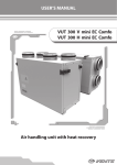
1
CPC308 PC/104-Plus Intel Atom N450/D510 Processor Module User Manual Ver. 0.4 December 2013 The product described in this manual is compliant with all related CE standards. CPC308 Processor Module Product Title: CPC308 Document name: CPC308 User Manual Manual version: 0.4 Copyright © 2012, 2013 Fastwel Co. Ltd. All rights reserved. Revision Record Rev. Index Brief Description Product Index Date 001 Initial version CPC308 June 2012 001a Partially corrected text CPC308 February 2013 001b Multiple text corrections CPC308 March 2013 001c ACS00041 accessory was excluded from the table 1-3, ACS00051 accessory was added to the table 1-3, purpose of contacts in ХР1 connector (table 3-4) was changed, section 7 was updated, errors were eliminated. CPC308 December 2013 0.4 Adjustment of subsection 2.3 Operating conditions. CPC308 December 2013 Contact Information Fastwel Co. Ltd Fastwel Corporation US 108 Profsoyuznaya st., Moscow 117437, Russian Federation 55 Washington St. #310 Tel.: +7 (495) 232-1681 +1 (718) 554-3686 Fax: +7 (495) 232-1654 +1 (718) 797-0600 Address: Brooklyn, New York 11201 USA Toll free: E-mail: [email protected] Web: http://www.fastwel.com/ C P C 3 0 8 U se r M a n u a l +1 (877) 787-8443 (1-877-RURUGGED) © 2 0 1 3 F a s t we l V e r . 0 0 1 b E 2 CPC308 Processor Module Contents Contents................................................................................................................................................................... 3 List of Tables............................................................................................................................................................ 5 List of Figures .......................................................................................................................................................... 6 Trademarks .............................................................................................................................................................. 7 Ownership Rights..................................................................................................................................................... 7 Safety Requirements ............................................................................................................................................... 8 High Voltage Safety Rules ............................................................................................................................ 8 Board Handling Instructions .......................................................................................................................... 8 General Board Operation Rules ............................................................................................................................... 9 The Manufacturer's Guarantees .............................................................................................................................. 9 1 Introduction .......................................................................................................................................... 11 1.1 1.2 2 Specifications ...................................................................................................................................... 14 2.1 2.2 2.3 2.4 2.5 2.6 3 The Purpose of the Product ........................................................................................................................ 11 Hardware Versions, Package Contents, Ordering Information ................................................................... 12 1.2.1 Hardware Versions, Ordering Information.................................................................................. 12 1.2.2 Package Contents ..................................................................................................................... 13 1.2.3 Additional Accessories ............................................................................................................... 13 Functional Structure of the Module ............................................................................................................. 14 Module Power Supply ................................................................................................................................. 15 Operating Conditions .................................................................................................................................. 16 Mechanical Characteristics ......................................................................................................................... 16 Weight and Dimensions .............................................................................................................................. 16 MTBF: ......................................................................................................................................................... 18 The Module Structure and Functioning ............................................................................................ 19 3.1 3.2 3.3 3.4 3.5 3.6 3.7 C P C 3 0 8 Block Diagram of the Module ...................................................................................................................... 19 The Module Main Elements Layout ............................................................................................................ 20 Operation Features of Functional Units ...................................................................................................... 22 Module Interfaces and Connectors ............................................................................................................. 24 3.4.1 PC/104-Plus Connectors ........................................................................................................... 24 3.4.2 Graphics Controller .................................................................................................................... 29 3.4.3 Audio Interface........................................................................................................................... 31 3.4.4 Serial Interfaces ......................................................................................................................... 32 3.4.5 USB Interfaces ........................................................................................................................... 36 3.4.6 Gigabit Ethernet Interface .......................................................................................................... 36 3.4.7 SerialATA Interface .................................................................................................................... 37 3.4.8 CompactFlash Connector .......................................................................................................... 38 3.4.9 PS/2 Keyboard/Mouse Interface ................................................................................................ 40 3.4.10 Power Connector ....................................................................................................................... 40 3.4.11 Discrete Input/Output Port ......................................................................................................... 41 3.4.12 External LEDs Connector (XP22) .............................................................................................. 43 3.4.13 Optically Isolated External Reset Input ...................................................................................... 44 3.4.14 System Reset Connector ........................................................................................................... 45 LED Indicators ............................................................................................................................................ 45 Watchdog Timers........................................................................................................................................ 46 The Module Address Space ....................................................................................................................... 46 3.7.1 Distribution of the Memory Address Space ................................................................................ 46 3.7.2 The Module Input/Output Address Space Distribution ............................................................... 47 3.7.3 Interrupt Lines Distribution ......................................................................................................... 48 U se r M a n u a l © 2 0 1 3 F a s t we l V e r . 0 0 1 b E 3 CPC308 Processor Module 4 CPC308 Module Installation ............................................................................................................... 49 4.1 4.2 4.3 4.4 4.5 5 Configuring CPC308............................................................................................................................ 54 5.1 5.2 5.3 5.4 6 7.3 7.4 7.5 7.6 7.7 7.8 Starting BIOS Setup Software .................................................................................................................... 61 Main ............................................................................................................................................................ 62 7.2.1 IDE Primary/Master.................................................................................................................... 62 7.2.2 SATA Port 1 – Port 3 ................................................................................................................. 63 7.2.3 Memory Cache .......................................................................................................................... 64 7.2.4 Boot Features ............................................................................................................................ 65 Advanced .................................................................................................................................................... 66 7.3.1 PnP Configuration ...................................................................................................................... 67 7.3.2 Console Redirection................................................................................................................... 68 7.3.3 I/O Device Configuration ............................................................................................................ 69 Intel ............................................................................................................................................................. 70 7.4.1 CPU Control Sub-Menu ............................................................................................................. 71 7.4.2 Video (Intel IGD) Control Sub-Menu .......................................................................................... 72 7.4.2.1 IGD – LCD Control Sub-Menu………………………………………………………………………73 7.4.3 ICH Control Sub-Menu............................................................................................................. 744 7.4.3.1 ICH USB Control Submenu…………………………………………………………………………75 Security ..................................................................................................................................................... 766 Boot .......................................................................................................................................................... 777 Custom ..................................................................................................................................................... 788 Exit ............................................................................................................................................................ 799 Transportation, Unpacking and Storage ........................................................................................... 80 8.1 8.2 8.3 A Work with WDT1 Watchdog Timer.............................................................................................................. 57 Work with WDT2 Watchdog Timer.............................................................................................................. 58 User LEDs Control: LED1, LED2 ................................................................................................................ 59 Discrete Input/Output Port Programming .................................................................................................... 59 Phoenix® BIOS .................................................................................................................................... 61 7.1 7.2 8 Selection of Buffers Power Voltage on the PCI Bus of PC/104-Plus Modules ............................................ 54 Selecting TFT Panel Power Voltage. .......................................................................................................... 54 Restoring Factory CMOS Settings (Clear CMOS) ...................................................................................... 55 BIOS Update............................................................................................................................................... 55 CPC308 Programming ........................................................................................................................ 57 6.1 6.2 6.3 6.4 7 Safety Requirements .................................................................................................................................. 49 Possible Heat Removal Methods ................................................................................................................ 50 The Procedure of CPC308 Installation ....................................................................................................... 50 The Procedure of the Module Dismounting ................................................................................................ 52 Installing Peripheral Devices onto the CPC308 Module ............................................................................. 52 4.5.1 Installing CompactFlash Memory Cards .................................................................................... 52 4.5.2 Connecting USB Devices........................................................................................................... 52 4.5.3 Battery Replacement ................................................................................................................. 53 4.5.4 Installing PC/104 and PC/104-Plus Expansion Modules............................................................ 53 Transportation............................................................................................................................................. 80 Unpacking ................................................................................................................................................... 80 Storage ....................................................................................................................................................... 80 Cooler Development Recommendations ........................................................................................ 811 C P C 3 0 8 U se r M a n u a l © 2 0 1 3 F a s t we l V e r . 0 0 1 b E 4 CPC308 Processor Module List of Tables Table 1-1: Ordering information ........................................................................................................................................ 12 Table 1-2: Package contents............................................................................................................................................. 13 Table 1-3: Additional accessories ..................................................................................................................................... 13 Table 2-1: Required Power Source Parameters ................................................................................................................ 15 Table 2-2: The Module Weight and Sizes ......................................................................................................................... 16 Table 3-1: XS1 PC/104-ISA Connector Contacts Designation .......................................................................................... 25 Table 3-2: Electrical Characteristics of the ISA Interface Lines ......................................................................................... 27 Table 3-3: The purpose of the PC/104-PCI (XS4) Connector Contacts ............................................................................ 28 Table 3-4: The Purpose of the VGA CRT (XP1) Connector Contacts ............................................................................... 30 Table 3-5: The Purpose of the LVDS (XP8) Connector Contacts ...................................................................................... 30 Table 3-6: The Purpose of the Audio Connectors Contacts .............................................................................................. 32 Table 3-7: The Purposes of COM1/COM2 (XP3 and XP6) Connectors Contacts ............................................................. 33 Table 3-8: The Purposes of COM3 and COM4 Connectors (XP17 and XP18) Contacts .................................................. 33 Table 3-9: The Purposes of USB1-USB4 Connectors (XP4, XP5) Contacts ..................................................................... 36 Table 3-10: The Purposes of the Gigabit Ethernet (XP11) Connector Contacts ............................................................... 37 Table 3-11: The Purposes of SATA Connectors (XP7 and XP10) Contacts ..................................................................... 37 Table 3-12: The Purposes of the CompactFlash (XP12) Connector Contacts .................................................................. 39 Table 3-13: The purposes of PS/2 (XP15) Connector Contacts ........................................................................................ 40 Table 3-14: The Purposes of the XP12 Power Connector Contacts ................................................................................. 41 Table 3-15: Discrete Input/Output Port Line Parameters in Output Mode ......................................................................... 41 Table 3-16: Discrete Input/Output Port Line Parameters in Input Mode ............................................................................ 42 Table 3-17: The Purposes of the XP24 Discrete Input/Output Port Connector Contacts .................................................. 42 Table 3-18: Purposes of the XP22 External LEDs Connector Contacts ............................................................................ 44 Table 3-19: The Purposes of LED Indicators .................................................................................................................... 45 Table 3-20: Distribution of the Memory Address Space .................................................................................................... 46 Table 3-21: Distribution of the Input/Output Address Space ............................................................................................. 47 Table 3-22: Interruption Lines Distribution......................................................................................................................... 48 Table 6-1: WDT1 Watchdog Timer Control Registers ....................................................................................................... 57 Table 6-2: WDT2 Watchdog Timer Control Registers ....................................................................................................... 58 Table 6-3: User Light Emitting Diode LED1 Control Register ............................................................................................ 59 Table A-1: Threshold Temperature Values of the Module Switching to Reduced Capacity Mode .................................. 811 C P C 3 0 8 U se r M a n u a l © 2 0 1 3 F a s t we l V e r . 0 0 1 b E 5 CPC308 Processor Module List of Figures Fig. 1-1: CPC308 processor module ordering template Fig. 2-1: Sizes and interface dimensions of the module (top view) Fig. 2-2: Module sizes (side view) Fig. 3-1: Block diagram of the module Fig. 3-2: Layout of connectors and principal components on the TOP side Fig. 3-3: Layout of connectors and principal components on the TOP side Fig. 3-4: XS1 PC/104-ISA Connector Contacts Fig. 3-5: PC/104-PCI (XS4) Connector Contacts Fig. 3-6: VGA CRT (XP1) connector Fig. 3-7: LVDS (XP8) Connector Fig. 3-8: XP19 audio connector Fig. 3-9: XP20 audio connector Fig. 3-10: COM1/COM2 (XP3 and XP6) Connectors Fig. 3-11: COM3 and COM4 ports connectors (XP17 and XP18) Fig. 3-12 "Point-to-point" type connection of two devices through RS 422 interface Fig. 3-13: Integration of several devices through the RS 485 interface Fig. 3-14: USB1-USB4 connectors (XP4, XP5) Fig. 3-15: Gigabit Ethernet (XP11) connector Fig. 3-16: SATA connectors (XP7 and XP10) Fig. 3-17: CompactFlash XP12 connector Fig. 3-18: PS/2 (XP15) Connector Fig. 3-19: XP25 power connector Fig. 3-20: XP24 Discrete input/output port connector Fig. 3-21: LEDs connection diagram Fig. 3-22: XP22 External LEDs Connector Fig. 3-23: XP21 optically isolated external reset input Fig. 3-24: Diagram of the module discrete input optical isolation realization Fig. 3-25: XP16 Reset Connector Fig. 3-26: User LED indicators on CPC308 board Fig. 3-27: Power indicator on CPC308 board Fig. 4-1: Heat removal methods Fig. 5-1: Status of the PCI VIO Selector (XP13) Switch Contacts Fig. 5-2: TFT Digital Panel Power Voltage Switch Fig. 7-1: Screen during module loading (POST) Fig. 7-2: "Main" Tab Menu Screen Fig. 7-3: “IDE Primary/Master” submenu screen Fig. 7-4: "Memory Cache" submenu screen Fig. 7-5: "Boot Features" submenu screen Fig. 7-6: "Advanced" Tab Menu Screen Fig. 7-7: "PnP Configuration" submenu screen Fig. 7-8: "Console Redirection" submenu screen Fig. 7-9: "I/O Device Configuration" submenu screen Fig. 7-10: "Intel" Tab Menu Screen Fig. 7-11: "CPU Control Sub-Menu" submenu screen Fig. 7-12: "Video (Intel IGD) Control Sub-Menu" submenu screen Fig. 7 13: IGD – LCD Control Sub-Menu Sub-Menu Screen Fig. 7-14: "ICH Control SUB-Menu" submenu screen Fig. 7-15: "ICH USB Control Sub-Menu" submenu screen Fig. 7-16: "Security" Tab Menu Screen Fig. 7-17: "Boot" Tab Menu Screen Fig. 7-18: "Custom" Tab Menu Screen Fig. 7-19: "Exit" Tab Menu Screen Fig. A-1: Heat sink temperature as a function of the ambient temperature when using a radiator (ACS00035-01 kit) C P C 3 0 8 U se r M a n u a l © 2 0 1 3 F a s t we l V e r . 0 0 1 b E 12 17 18 19 21 22 24 27 29 30 31 31 33 33 34 35 36 36 37 38 40 41 42 43 43 44 45 45 45 45 50 54 55 61 62 63 64 65 66 67 68 69 70 71 72 73 744 755 766 777 788 799 811 6 CPC308 Processor Module Trademarks "Fastwel" logotype is a trademark belonging to Fastwel Group Co. Ltd., Moscow, Russian Federation. Besides, this document may contain names, corporate logotypes and trade marks being registered trade marks; consequently, property rights to them belong to their respective legitimate owners. Ownership Rights This document contains information being the property of Fastwel Group Co. Ltd. It can neither be copied nor transferred with the utilization of known media nor be stored in data storage and search systems without the prior written authorization of Fastwel Group Co. Ltd. To our best knowledge, the data in this document does not contain errors. However, Fastwel Group Co. Ltd cannot take responsibility for any inaccuracies and their consequences, as well as responsibility arising as a result of utilization or application of any diagram, product or example cited in this document. Fastwel Group Co. Ltd reserves the right to alter and update both this document and the product presented therein at its own discretion without additional notification. C P C 3 0 8 U se r M a n u a l © 2 0 1 3 F a s t we l V e r . 0 0 1 b E 7 CPC308 Processor Module Safety Requirements This product of Fastwel Group Co. Ltd has been developed and tested with the purpose of ensuring its compliance with electrical safety requirements. Its design provides long-term troublefree functioning. The product service life can be significantly shortened because of its incorrect handling during unpacking and installation. Therefore, for your safety and ensuring of the correct operation of the product you should adhere to the recommendations given below. High Voltage Safety Rules Any work with this device must be performed only by sufficiently skilled personnel. Before installing the board into your system, make sure that the mains power supply is disconnected. This is also true for the installation of expansion boards. There is a serious hazard of electrocution in the process of the product installation, repair and maintenance; therefore, always unplug the power cord during work performance. This is also true for other power cables. Board Handling Instructions Electronic boards and their components are static sensitive. Therefore, special attention is needed to ensure safety and normal operation while handling those devices. C P C 3 0 8 Do not leave the board without protective package when it does not operate. Always work with the board on static-safe workplaces if possible. If it is impossible, the user must remove static charge from him/herself before touching the product with his/her hands or tools. This is best done by touching a metal part of the system body. It is especially important to observe precaution while replacing expansion boards, jumpers, etc. Since there is a battery powering memory and real-time clock on the board, do not put it on conductive surfaces, like antistatic carpets or sponges. They may cause a short circuit and inflict damage to the battery and the board conductors, as well as loss of real-time clock (RTC) data. U se r M a n u a l © 2 0 1 3 F a s t we l V e r . 0 0 1 b E 8 CPC308 Processor Module General Board Operation Rules To preserve the manufacturer's guarantee, the product must not be reworked or altered in any way. Any alterations and improvements not authorized by Fastwel Group Co. Ltd company, except those described in this Manual or obtained from the Fastwel Group Co. Ltd technical support service in the form of a set of instructions describing their performance cancel the guarantee. This device must be only installed into and connected to systems meeting all necessary technical and climatic requirements. This relates to the operating temperatures range of the specific board design version. The temperature limitations of the batteries installed on the board should be taken into account as well. Please follow only the instructions of this Manual while performing all necessary installation and configuring operations. Keep original package to store the product in the future or to transport it in case of a guarantee event. Should it become necessary to transport or store the board, pack it in the same way it was packed upon receipt. Take particular care during handling the product and its unpacking. Act in accordance with the instructions of the above section and Chapter 8 Transportation, Unpacking and Storage. The Manufacturer's Guarantees Guarantee Liabilities The Manufacturer hereby guarantees the product conformity with the requirements of TU 4013-004-52415667-05 specifications, provided the Consumer abides by the conditions of operation, transportation, storage, installation and assembly established by the accompanying documents. The Manufacturer hereby guarantees that the products supply thereby are free from defects in workmanship and materials, provided operation and maintenance norms were observed during the currently established guarantee period. The Manufacturer's obligation under this guarantee is to repair or replace free of charge any defective electronic component being a part of a returned product. Products that broke down through the Manufacturer's fault during the guarantee period will be repaired free of charge. Otherwise the Consumer will be invoiced as per the current labor remuneration rates and expendable materials cost. Liability Limitation Right The Manufacturer shall not be liable for the damage inflicted to the Consumer's property because of the product breakdown in the process of its utilization. Guarantee Period The guarantee period for the products made by the manufacturer company is 36 months since the sale date (unless otherwise provided by the supply contract). The guarantee period for the products made to special order is 60 months since the sale date (unless otherwise provided by the supply contract). C P C 3 0 8 U se r M a n u a l © 2 0 1 3 F a s t we l V e r . 0 0 1 b E 9 CPC308 Processor Module The warranty set forth above does not extend to and shall not apply to: 1. Products, including software, which have been repaired or altered by other than Fastwel personnel, unless Buyer has properly altered or repaired the products in accordance with procedures previously approved in writing by Fastwel. 2. Products, which have been subject to power supply reversal, misuse, neglect, accident, or improper installation. Returning a product for repair 1. Apply to Fastwel company or to any of the Fastwel's official representatives for the Product Return Authorization. 2. Attach a failure inspection report with a product to be returned in the form, accepted by customer, with a description of the failure circumstances and symptoms. 3. Carefully package the product in the antistatic bag, in which the product had been supplied. Failure to package in antistatic material will VOID all warranties. Then package the product in a safe container for shipping. 4. The customer pays for shipping the product to Fastwel or to an official Fastwel representative or dealer. C P C 3 0 8 U se r M a n u a l © 2 0 1 3 F a s t we l V e r . 0 0 1 b E 10 СРС308 Processor Module Introduction 1 Introduction 1.1 The Purpose of the Product This Operation manual (hereinafter, the Manual) is intended to inform about the design, operation and basic information necessary for the commissioning, proper use and maintenance of the product known as CPC308 Processor Module (hereinafter, the module). NOTE: THIS DOCUMENT PRESENTS THE ACTIVE VERSION 0.1 OF THE MANUAL. The module is a single-board, PC/104-Plus format computer. It is intended for onboard applicationы requiring high performance and low power consumption. The module has a CompactFlash connector, two Ethernet channels, two USB ports, two Serial ATA ports, four serial ports and NAND Flash data storage. It is possible to expand the module functionality by connecting complementary PC/104 and PC/104-Plus format modules. The module is delivered with pre-installed FreeDOS operation system (hereinafter, the OS). It is compatible with the following OSs: 2) QNX 6.5, Windows XP (embedded) and Linux 2.6. The Manual gives instructions on correct and safe installation, enabling and configuring of the module, its connection to and interaction with expansion modules or external devices. The Manual also covers the matters of starting, debugging and running programs from among basic and utility software (hereinafter, the Software). For safe and correct operation of the module during its established service life, one must familiarize oneself with this manual beforehand. WARNING: THE MODULE OPERATION WITHOUT OBSERVING SAFETY REQUIREMENTS, UTILIZATION AND OPERATION INSTRUCTION IS NOT PERMITTED! 3) ATTENTION: THE MODULE CONTAINS STATIC SENSITIVE COMPONENTS! 4) FORBIDDEN: OPERATION, MAINTENANCE AND REPAIRS OF THE MODULE BY PERSONS LACKING THE RESPECTIVE SKILLS AND THE REQUIRED LEVEL OF SPECIAL TRAINING! 5) The graphic symbol (sign) is hereinafter used together with the explanatory word "Note" explanation text. 2) Unless operating system presets were ordered separately. See Table 1-1 below. 3) The graphic symbol (safety sign as per GOST R 12.4.026-2001) is hereinafter used jointly warning word "WARNING" and the warning text (as per GOST 2.601-2006). 4) The graphic symbol (safety sign as per GOST R 12.4.026-2001) is hereinafter used jointly warning word "ATTENTION" and the warning text (as per GOST 2.601-2006). 5) The graphic symbol (safety sign as per GOST R 12.4.026-2001) is hereinafter used jointly warning word "FORBIDDEN" and the warning text (as per GOST 2.601-2006). C P C 3 0 8 U se r M a n u a l © 2 0 1 3 F a s t we l V e r . 0 0 1 b E and the with the with the with the 11 СРС308 Processor Module Introduction 1.2 Hardware Versions, Package Contents, Ordering Information 1.2.1 Hardware Versions, Ordering Information The module hardware versions and their designation for the purposes of ordering (ordering information) are shown in the table and the figure below: Table 1-1: Ordering information Conventional designation Name CPC308 processor module CPС308 Ordering designation CPC308-01 1) CPC308-03 2) Note Intel Pineview N450/1GB DDR2 RAM/ 4GB NAND Flash/ Compact Flash/ 2xSATA/ Discrete IO/ 2x Ethernet/ 4x USB 2.0/ 2x RS232/ 2x RS422/485/ VGA/ LVDS Intel Pineview D510/1GB DDR2 RAM/ 4GB NAND Flash/ Compact Flash/ 2xSATA/ Discrete IO/ 2x Ethernet/ 4x USB 2.0/ 2x RS232/ 2x RS422/485/ VGA/ LVDS Module option with a preinstalled Linux 2.6. operating system 3) CPC308-xx\LNX CPC308-xx\yy\Coated 4) A moisture protected module option 1) The module contains a complete set of hardware interfaces and functional elements. Unlike CPC308-01, the module has an Intel Pineview D510 dual core processor installed. 3) Where xx – is the module version (01, 03). 4) Where yy – is the operating system (LNX) preinstallation option. 2) Fig. 1-1: CPC308 processor module ordering template C P C 3 0 8 U se r M a n u a l © 2 0 1 3 F a s t we l V e r . 0 0 1 b E 12 СРС308 Processor Module 1.2.2 Introduction Package Contents Package contents for all the module versions are shown in the table below: Table 1-2: Package contents Ordering designation Decimal number Description CPС308-01, CPC308-03. ИМЕС.467444.308, ИМЕС.467444.308-02 CPC308 processor module ACS00023 – Adapter cable (DB9F – IDC10) for connecting to XP3, XP6 (СОМ1, COM2) connectors ACS00027 – Adapter cable (DB15F – IDC10) for VGA monitor connecting to XP connector ACS00043 – Adapter cable for connecting a PS/2 keyboard and mouse to XP15 connector ACS00057 – Power socket with contacts for connecting to XP25 power connector – – Package 1.2.3 Additional Accessories Additional accessories for connecting to the module are shown in the table below. Table 1-3: Additional accessories Ordering designation ACS00031-01 ACS00031-02 ACS00031-03 ACS00037 ACS00040-01 ACS00040-04 Description ACS00031-01 installation kit. The kit includes a JST PHR-5 socket and a SPH-002TP0.5S set of contacts for connecting to XP18 and XP19 (COM3, COM4, Audio) connectors of the module ACS00031-02 installation kit. The kit includes a JST PHR-6 socket and a SPH-002TP0.5S set of contacts for connecting to XP15 (KB/Mouse) connector of the module ACS00031-03 installation kit. The kit includes a JST PHR-2 socket and a SPH-002TP0.5S set of contacts for connecting to XP20, XP21 (Mic In, Opto Reset) connectors of the module ACS00037 installation kit. The kit includes a Hirose DF13-20DS-1.25C socket and a DF13-2630SCF set of contacts for connecting to XP8 (LVDS) connector of the module ACS00040-01 installation kit. The kit includes a Leotronics 2040-3102 socket for connecting to XP3, XP6, XP4, XP5, XP1 (COM1, COM2, USB1,2, USB3,4, VGA) connectors of the module ACS00040-04 installation kit. The kit includes a Leotronics 2040-320 socket for connecting to XP11 (2xEthernet) connector of the module ACS00051 Cable IDC2-10 – 2xUSBA for the connection to XP4, XP5 (USB) ACS00035-01 A radiator and installation screws. C P C 3 0 8 U se r NOTE: M a n u a l ADDITIONAL ACCESSORIES FOR CONNECTING TO THE MODULE ARE NOT DELIVERED WITH IT; THEY ARE PURCHASED SEPARATELY. © 2 0 1 3 F a s t we l V e r . 0 0 1 b E 13 СРС308 Processor Module 2 Specifications 2.1 Functional Structure of the Module Specifications The module includes the following basic functional elements: Intel Pineview-M (N450)1) or Intel Pineview-D (D510)2) microprocessor: – Single 32/64-bit x86 core (for N450), – Two 32/64-bit x86 cores (for D510), – SSE2, SSE3, SSSE3 support, – Hyperthreading support, – 64-bit memory bus, – Level I cache - 32 KB programs area, 24 KB data area), – Level II cache - 512 KB (for N450), – Level II cache - 1 MB (for D510), – Intel SpeedStep technology support (for N450); DDR2 SDRAM 667 MHz system memory (soldered) - 1 GB; Flash BIOS: – 16 Mbit, – In-system modification possible; Two SATA interfaces: two standard onboard connectors; NAND Flash storage (soldered and connected to the SATA interface) - 4 GB; CompactFlash connector: – Type I / Type II devices support, – UDMA mode support; Video controller: – 2D/3D accelerator, – Video memory size (allocated from system memory) – 256 MB max, – Connectivity for LCD panels (LVDS 18-bit) with resolution up to 1280 x 800 (60 Hz) and VGA interface monitors with resolution up to 1400 x 1050 (60 Hz)3), – Connectivity for LCD panels (LVDS 18-bit) with resolution up to 1366 x 768 (60 Hz) and VGA interface monitors with resolution up to 2048 x 1536 dots (60 Hz)4), Two 10/100/1000 Mb Ethernet controllers USB ports: – Up to four devices; – USB 1.1 and USB 2.0 specifications support; – Supported OS loading from USB media; Serial ports: – СОМ1, COM2: RS 232, nine-cable (complete) console input/output enabled, maximum data exchange rate 115.2 Kbit/s, 1) Installed in the CPC308-01 module Installed in the CPC308-03 module 3) For CPC308-01 module 4) For CPC308-03 module 2) C P C 3 0 8 U se r M a n u a l © 2 0 1 3 F a s t we l V e r . 0 0 1 b E 14 СРС308 Processor Module Specifications – COM3, COM4: RS 422/485, galvanically isolated (breakdown voltage 500 V), maximum data exchange rate 9221 Kbit/s; HD Audio controller; – Stereo line input/output, – Microphone input; PS/2 keyboard and mouse port; Discrete input/output port: – 8 separately programmable input/output lines; Optically isolated external reset/interrupt input: – dielectric breakdown voltage - 500 V; Real time clock (RTC); CMOS+Serial FRAM (for system configuration storage); Two watchdog timers (WDTs): – WDT1 - with a fixed timeout period - 1.6 s, – WDT2 - with a programmable timeout period - from 1 to 255 minutes; The module is software compatible with the following OS: FreeDOS, QNX 6.5, Windows XP (embedded), Linux 2.6. 2.2 Module Power Supply Electric power supply of the module must meet the requirements cited in the table below. The module may be powered through both the power connector (XP25) and through the PC/104 bus connector. The module's maximum current consumption value is 3.1 A 1) without external devices. Table 2-1: Power Supply Requirements Output voltage, V From +4.75 to +5.25 1) Rated load current, A Output buildup time to the +4.75 V level, ms 6 Maximum 10 For CPC308-03 module C P C 3 0 8 U se r M a n u a l © 2 0 1 3 F a s t we l V e r . 0 0 1 b E 15 СРС308 Processor Module 2.3 Specifications Operating Conditions The module must be used under the following operating conditions: – Operating temperature range: –40 to +85°С , 1) Modules are resistant to alteration (change) of ambient temperature in the specified temperature range, at relative humidity up to 80%, without moisture condensation. USE THE MODULE AT AMBIENT TEMPERATURE EXCEEDING 70°С WITHOUT ACS00035-01 ACCESSORY OR ANOTHER HEATSINK ATTACHED TO THE HEAT-SPREADING PLATE (ANOTHER RADIATOR, THE DEVICE BODY, ETC.). FORBIDDEN: 2.4 Mechanical Characteristics The module has the following mechanical characteristics: – Vibration resistance: 5g max. – Single shock resistance: 100 g max. – Multiple shock resistance: 50 g max. 2.5 Weight and Dimensions The weight and dimension values for various hardware versions of the module are shown in the table below: Table 2-2: The Module Weight and Sizes Module Weight, kg, max. CPC308 0.3 1) 1) Without CompactFlash device. Weight, kg, in package Dimensions, mm, max. 0,484± 0,05 116* x 96* x 29* 2) Package dimensions, mm, 2) 230x155x45 mm “*” - dimensions for reference. The general sizes and interface dimensions of the module are shown on figures below. 1) The value of the top temperature limit (plus 85°С) is valid when the module is used with the ACS00035-01 accessory or when it is used as a part of a cabinet device where heat is withdrawn from the heat-spreading plate to the device body. C P C 3 0 8 U se r M a n u a l © 2 0 1 3 F a s t we l V e r . 0 0 1 b E 16 СРС308 Processor Module Specifications Fig. 2-1: Overall and Mounting Dimensions of the Module (Top View) C P C 3 0 8 U se r M a n u a l © 2 0 1 3 F a s t we l V e r . 0 0 1 b E 17 СРС308 Processor Module Specifications Fig. 2-2: Dimensions (Side View) 2.6 MTBF: The MTBF value for the module is 120,000 hours. C P C 3 0 8 U se r NOTE: M a n u a l THIS MTBF VALUE HAS BEEN CALCULATED ACCORDING TO THE TELCORDIA ISSUE 1 CALCULATION MODEL, METHOD I CASE 3 CALCULATION PROCEDURE, FOR CONTINUOUS OPERATION ON EARTH UNDER THE CONDITIONS MEETING UKHL4 UNDER GOST 15150-69, AT AMBIENT TEMPERATURE +30С. © 2 0 1 3 F a s t we l V e r . 0 0 1 b E 18 СРС308 Processor Module The Module Structure and Functioning 3 The Module Structure and Functioning 3.1 Block Diagram of the Module Block diagram of the module is shown below: Fig. 3-1: Block Diagram of the Module Soldered DDR2 SDRAM 1GB XP5 Pineview-M / Pineview-D USB 1,2 Soldered NAND FLASH 4GB VGA CRT XP1 SATA NAND FLASH Controller LVDS XP8 x4 DMI Compact Flash SATA Port 3 XP4 IDE USB 3,4 ICH8-M Gigabit LAN 1,2 XP11 SPI BIOS PCI 32bit Bus 16Mbit AUDIO (IN,OUT) XP19 Gigabit Ethernet i82574 Digital I/O XP24 Isolated IRQ/Reset Opto-isolation PCIE-6 Super I/O SMSC SCH3114 SMBus GPIO Opto-isolation XP25 PCIE-5 HD Audio Codec External LEDS XP22 XP21 Gigabit Ethernet i82574 AUDIO (MIC) XP20 XP12 CK-505 & SS Clocking DC +5V IN Supervisor WDT DC/DC 3.3V VR FRAM PCI-ISA Bridge SMBus SATA Port1 XP7 SATA Port2 XP10 RS485 COM3 XP17 RS485 COM4 XP18 RS232 COM1 XP3 RS232 COM2 XP6 PS/2 port XP15 PCI BUS 32-bit XS4 ISA BUS 16-bit XS1 CPU Core VR Chipset VR Memory VR C P C 3 0 8 U se r M a n u a l © 2 0 1 3 F a s t we l V e r . 0 0 1 b E 19 СРС308 Processor Module The Module Structure and Functioning The following functional elements are shown in the module block diagram: – Intel Atom N450 or Intel Atom D510 microprocessor (depending on the module version); – DDR2 SDRAM system memory (up to 1 GB); – Flash BIOS (16 Mbit); – NAND Flash data storage (4 GB); – VGA monitor port (XP1); – LVDS interface connector for TFT panel connecting (XP8); – 2 SATA channels (XP7 and XP10); – CompactFlash connector (XP12); – Two 10/100/1000 Mb Ethernet channels (XP11); – 4x USB 2.0 channels (XP4 and XP5); – СОМ1 (RS232) (XP3), COM2 (RS 232) (XP6), COM3 (RS422/285) (XP17), – – – – – – – – – COM4 (RS 422/485) serial ports (XP18); PS/2 keyboard and mouse port (XP15); Discrete input/output port (XP24); External indication connector (XP22); HD Audio controller with line input/output and microphone connectors (XP19 and XP20); External optoisolated reset (XP21); 16 bit ISA bus (XS1); 32 bit, 33 MHz PCI bus(XS4); Serial FRAM (for system configuration storage); Two watchdog timers (WDTs). Technical features of the module's main functional elements are described in subsection 2.1 of the Manual. 3.2 The Module Main Elements Layout The layout of main components, their corresponding connectors, as well as jumper switches for top and bottom sides is shown, respectively, in Fig. 3-2 and Fig. 3-3. The default positions of jumpers in jumper switches are also shown in Fig. 3-2, and jumpers settings by functions are shown in Section 5 Configuring CPC308. C P C 3 0 8 U se r M a n u a l © 2 0 1 3 F a s t we l V e r . 0 0 1 b E 20 СРС308 Processor Module The Module Structure and Functioning Fig. 3-2: Layout of Connectors and Main Components (Top Side) Isolated IRQ/Reset Selector (XP23) PCI BUS (XS4) 1 Audio IN/OUT (XP19) HD Audio Audio MIC (XP20) LTM2881 uModule LINEAR Reset (XP16) LINEAR LVDS Panel LVDS Power Selector (XP8) Isolated Isolated (XP2) VGA COM4 COM3 (XP1) (XP18) (XP17) LTM2881 uModule SATA1 (XP7) SATA2 (XP10) Isolated IRQ/Reset (XP21) 8Mx16x8 ISA 16bit BUS (XS1) 8Mx16x8 1 CMOS Reset (XP9) 8Mx16x8 PC/104 (PCI) PCI VIO Selector (XP13) External LEDs (XP22) HCS0905H 1 Discrete I/O (XP24) 8Mx16x8 SM2242T AC 1 A1 B1 A1 1 D1 SCH3114 Power LED (HL3) User LED1 Green (HL1) User LED2 Yellow (HL2) PS/2 KB/MS (XP15) Pulse 1 USB3,4 (XP5) USB1,2 (XP4) C P C 3 0 8 U se r M a n u a l 1 1 1 COM2 COM1 (XP6) (XP3) HX5020NL Gigabit Ethernet 1,2 (XP11) © 2 0 1 3 Power (XP25) F a s t we l V e r . 0 0 1 b E 21 СРС308 Processor Module The Module Structure and Functioning Fig. 3-3: Layout of Connectors and Main Components (Bottom Side) 8Mx16x8 Atom N450 8Mx16x8 8Mx16x8 Super IO AMD Geode LX PCI to ISA Bridge 8Mx16x8 NAND Flash CS5536 i82574 i82574 3.3 Compact Flash (XP12) NAND Flash ICH8 Operation Features of Functional Units Intel PineView-M (-D) An energy efficient (~5.5 W) 32-bit Intel microprocessor built on Atom core1). A highly integrated solution uniting the processor core itself, as well as the SDRAM/DDR2 controller and a 3D/2D accelerated graphic adapter. ICH-8M A highly integrated interface controller including standard IBM PC AT platform peripherals. Memory A 1 GB DDR2-667 RAM is soldered on board. The installation of memory expansion modules is not supported. BIOS A Flash 16 microchip on the SPI bus is used for BIOS storage. RTC, CMOS 1) In case of Intel Pineview-M (N450) processor C P C 3 0 8 U se r M a n u a l © 2 0 1 3 F a s t we l V e r . 0 0 1 b E 22 СРС308 Processor Module The Module Structure and Functioning The real time clock is built in ICH8. The clock operability without power is ensured by a lithium battery installed on the board. BIOS Setup settings are saved in the FRAM. FRAM 64-Kbit non-volatile memory, may be used to save user data and store BIOS Setup parameters. NAND Flash NAND Flash microchips having total volume up to 4 GB are soldered on board. The NAND Flash connection to the SATA bus (SATA Flash Disk Controller is used) permits to increase operation speed and ensure compatibility with various OSs. A two-channel NAND Flash operation mode is supported. CompactFlash The module permits to use CompactFlash (Type I/II) cards as a data storage, the socket is placed on the bottom side for that purpose. Ethernet Two 10/100/1000 Mbit PCIe Ethernet controllers built on Intel i82574 microchip are used, both channels are connected to a joint IDC20 connector on the board having 2 mm contact spacing. USB 2.0 The board has 4 USB 2.0 channels: They are connected to two IDC 10 type connectors having 2 mm contact spacing installed on the board. COM1/COM2/COM3/COM4 COM1/COM2 – 9-wire RS232 interface. Each port is connected to an IDC 10 type board connector with 2 mm contact spacing. COM3/COM4 - galvanically isolated RS422/485, insulation voltage up to 500 V. The transmitter is controlled in an automatic mode. Each port is connected to a straight 5-pin connector with 2 mm contact spacing. Termination resistors (RS422/485) can be connected with the help of BIOS Setup software. PS/2 Keyboard & Mouse Intended for connecting a PS/2 keyboard and a mouse to the module, a straight single-in-line 6-pin connector having 2 mm contact spacing is used for that purpose. SATA Two SATA interfaces: both standard connectors are placed on the board. VGA, LVDS The ports are intended for connecting a VGA analog monitor and/or a LVDS interface matrix. Dualmonitor configurations are supported in clone/extended desktop modes. Audio The support is realized with the help of HD Audio codec. The following signal connectors are installed on the board: line input, line output (a 5-pin connector with 2 mm contact spacing), as well as a microphone input (a 3-pin connector with 2 mm contact spacing). Indication There are power-on indication LEDs placed on the board, as well as two programable LEDs for user needs. External LEDs may be connected through a connector on the board. This connector allows to connect the following LEDs: disc storages activity, indication of LAN1 and LAN1 ports connection and activity, LED1 and LED2 user LEDs, a power-on indicator. Watchdog There are two watchdog timers in the module. One of them (WDT1) is built into the supervisor microchip and has a fixed timeout period (1.6 s), the other is built into the SIO microchip; it has programmable timeout period (up to 255 min). C P C 3 0 8 U se r M a n u a l © 2 0 1 3 F a s t we l V e r . 0 0 1 b E 23 СРС308 Processor Module The Module Structure and Functioning Reset and Power Monitoring The microprocessor reset signal is formed from the following sources: Supervisor when power is turned on; "Reset" button; Watchdog timers. Jumpers The following functional selectors are placed on the board: Isolated discrete input operation mode selector (Reset/Interrupt) XP23; LVDS panel power selector (XP2) PCI VIO selector (XP13); CMOS Reset selector (XP9). 3.4 Module Interfaces and Connectors 3.4.1 PC/104-Plus Connectors There are standard PC/104-Plus format connectors installed in the CPC308 module. With their help CP308 can be connected to such devices as analog-digital converters, digital input/output modules, etc. As per the PC/104-Plus specification, the module includes PC/104-ISA and PC/104-PCI connectors described below. PC/104-ISA Interface PC/104-ISA interface permits the module to operate with 8- or 16-digit PC/104 expansion modules. A 104-pin 0.10" (2.54 mm) connector located on the top side of the module is used for the PC/104 bus. Through that connector ISA bus signals are transmitted at 8 MHz frequency. The CPC308 processor module supports up to four PC/104 expansion modules without additional bufferization. The layout and designation of the PC/104-ISA connector contacts is shown in a figure and in tables below. Fig. 3-4: XS1 PC/104-ISA Connector Contacts B1 A1 B32 A32 C0 D0 C P C 3 0 8 U se r M a n u a l C19 D19 © 2 0 1 3 F a s t we l V e r . 0 0 1 b E 24 СРС308 Processor Module The Module Structure and Functioning Table 3-1: XS1 PC/104-ISA Connector Contacts Designation C P C 3 0 8 U se r M a n u a l © 2 0 1 3 F a s t we l V e r . 0 0 1 b E 25 СРС308 Processor Module The Module Structure and Functioning Note: Designation "–" is not used in these tables. The "Status" column shows the direction of the data transfer for the processor module being the bus master. The table below cites electrical characteristics of the ISA interface lines. C P C 3 0 8 U se r M a n u a l © 2 0 1 3 F a s t we l V e r . 0 0 1 b E 26 СРС308 Processor Module The Module Structure and Functioning Table 3-2: Electrical Characteristics of the ISA Interface Lines Symbol VIL VIL Parameter Input Low Voltage for 5V cell Input Low Voltage for 3.3V cell Conditions Min. Typical Max. Units TTL 0.8 V CMOS 0.3*VC C3 V VIL Schmitt Input Low Voltage TTL VIH Input Low Voltage for 5V cell TTL 2.2 V VIH Input Low Voltage for 3.3V cell CMOS 0.7*VCC3 V VIH Schmitt Input Low Voltage VIH Input Low Voltage for 5V cell 0.4 V VOL Input Low Voltage for 3.3V cell 0.4 V VOH Output High Voltage for 5V cell 3.5 V VOH Output High Voltage for 3.3V cell 2.3 V VIL Input Low Current no P/D or P/U -1 1 μA IIH Input High Current no P/D or P/U -1 1 μA IOZ Tri-state Leakage Current -10 10 μA CIN Input Capacitance 1.10 TTL V 1.87 V 3 ρF COUT Output Capacitance 3 to 6 ρF CBID Bi-directional buffer Capacitance 3 to 6 ρF PC/104-PCI Interface PC/104-PCI interface uses a 120-pin (30x4) XS4 connector located on the top side of the board. It is used to transmit all the necessary signals of the 32-bit PCI bus at 33 MHz frequency. Three Bus Master devices are supported. The layout of the PC/104-PCI connector contacts is shown in a figure below. The designation of the connector contacts is described in Table 3-3: The Designation of the PC/104-PCI (XS4) Connector Contacts. Fig. 3-5: PC/104-PCI (XS4) Connector Contacts C P C 3 0 8 U se r M a n u a l © 2 0 1 3 F a s t we l V e r . 0 0 1 b E 27 СРС308 Processor Module The Module Structure and Functioning Table 3-3: The Designation of the PC/104-PCI (XS4) Connector Contacts PCI VIO Selector switch (XP13) is located on the top side of the board (near the XS4 connector, see Fig. 3 2: Layout of Connectors and Main Components on the Top Side). It is used to select power voltage of PC\104-Plus modules PCI interface buffers. The following states of the XP13 switch contacts are possible: Contacts 1-2 closed – PCI bus signal level is +5 V; Contacts 2-3 closed – PCI bus signal level is +3.3 V; C P C 3 0 8 U se r M a n u a l © 2 0 1 3 F a s t we l V e r . 0 0 1 b E 28 СРС308 Processor Module The Module Structure and Functioning All contacts open - signal levels are selected at the PC/104-Plus power source. XP13 switch is described in more detail in subsection 5.1 Selection of Buffers Power Voltage on the PCI Bus of PC/104-Plus. Pay attention to the note: Note If you use a PC/104-Plus power source, the VIO voltage must be set at the power supply module. In this case remove the jumper from the VIO (XP13) selector switch: all contacts should be open. If a PC/104-Plus power supply is not used, the jumper on the XP13 selector switch must be put into the 1-2 or 2-3 position, see Fig. 5-1: Status of the PCI VIO Selector (XP13) Switch Contacts. 3.4.2 Graphics Controller The Intel Pineview microprocessor is a highly integrated solution uniting the processor core itself, as well as the SDRAM/DDR2 controller and a 3D/2D accelerated graphics adapter. It enables the module to efficiently process 2D/3D graphics. A built-in graphics controller permits to connect the module directly to a standard analog monitor through the VGA connector on the board and/or with digital TFT panels through a LVDS connector. Dual-monitor configurations are supported in clone/extended desktop modes. 3.4.2.1 VGA CRT Interface A 10-pin XP1 IDC10 type connector with 2 mm contact spacing is installed on the top side of the board to connect an analog monitor to CPC308. – It is possible to connect VGA interface monitors having a resolution up to 1400 x 1050 (60 Hz) (for CPC308-01 modules); – it is possible to connect VGA interface monitors having a resolution up to 2048 x 1536 (60 Hz) (for CPC308-03 modules); Fig. 3-6: VGA CRT (XP1) Connector C P C 3 0 8 U se r M a n u a l © 2 0 1 3 F a s t we l V e r . 0 0 1 b E 29 СРС308 Processor Module The Module Structure and Functioning Table 3-4: Designation of the VGA (XP1) Connector Contacts Contact 1 2 3 4 5 Signal RED GND GREEN GND BLUE Contact 6 7 8 9 10 Signal GND HSYNC VSYNC - A monitor is connected either with the help of the ACS00027 accessory delivered with the module or with the help of a self-made cable. It is recommended to use a 2040-3102 Leotronics socket or the ACS00040-01 from additional accessories (see Table 1 3). 3.4.2.2 LVDS Interface There is a 20-pin LVDS interface connector located on the top side of the board. It is intended for connection of digital TFT-panels with cables crimped for 1.25 contact spacing. Supported mode: Single LVDS, up to 18 bit/pixel, 25-112 MHz frequency range. – – It is possible to connect LCD panels (LVDS 18-bit) having a resolution up to 1280x800 (60 Hz) (for CPC308-01 modules); It is possible to connect LCD panels (LVDS 18-bit) having a resolution up to 1366x768 (60 Hz) (for CPC308-01 modules); Fig. 3-7: LVDS (XP8) Connector 20-pin LVDS connector for connecting digital TFT panels Table 3-5: The Designation of the LVDS (XP8) Connector Contacts To make a custom a cable, it is recommended to use either a DF13-20DS-1.25C (Hirose) type connector having DF13-2630SCF (Hirose), or an ACS00037 accessory (see Table 1 3). 3.4.2.2.1. Power Voltage Selection for a Digital TFT Panel Standard tri-contact selector switch XP2 is intended to select digital panel power voltage (see Fig. 3 2: Layout of Connectors and Main components on the Top Side). C P C 3 0 8 U se r M a n u a l © 2 0 1 3 F a s t we l V e r . 0 0 1 b E 30 СРС308 Processor Module The Module Structure and Functioning TFT panel power voltage selection is described in detail in section 5.2 Selecting TFT Panel Power Voltage. If contacts 1-2 are closed, the digital panel is powered by +3.3 V voltage. If contacts 2-3 are closed, it is powered by +5 V voltage. Attention! Be very careful when selecting the TFT panel power voltage! Incorrect power voltage setting may make the panel inoperative. To define the exact value of the TFT panel power voltage, please look at the reference information provided by the panel manufacturer or inquire the dealer from whom you have bought the panel. 3.4.3 Audio Interface There are two audio connectors for wire crimp (support is realized with the help of HD Audio codec): For line input and line output signals (XP19, 5-pin connector with 2 mm contact spacing); For microphone input signals (XP20, 2-pin connector with 2 mm contact spacing) Fig. 3-8: XP19 Audio Connector Fig. 3-9: XP20 Audio Connector The designation of audio connectors contacts are specified in the table below. C P C 3 0 8 U se r M a n u a l © 2 0 1 3 F a s t we l V e r . 0 0 1 b E 31 СРС308 Processor Module The Module Structure and Functioning Table 3-6: The Designation of the Audio Connectors Contacts To make adapter cables for connecting to XP19 and XP20 connectors, it is recommended to use either PHR-5 (JST) / PHR-2 (JST) respectively for cables crimp with SPH-002T-P0.5S (JST) contacts, or ACS00031-01 and ACS00031-03 accessories, respectively (see Table 1 3). 3.4.4 Serial Interfaces The module has four serial ports: COM1 – COM4. 3.4.4.1 COM1 and COM2 Ports COM1 and COM2 ports operate in complete (nine-cable) RS232 interface mode. They have standard PC/AT base addresses (see Table 3 21) and interrupts (see Table 3 22). The ports can be also used for console input/output. The number of the COM port for a remote console connection to COM1 (XP3) or COM2 (XP6) is selected with the help of the respective BIOS Setup module setting (see subsection 7.3.2 Console Redirection). To communicate with a remote console (PC emulating a terminal with the data exchange parameter for a COM port: 115200 bps, 8, N, 1), use connection through the "null-modem" cable1) and the ASC00023 cable delivered with the module, e.g. to the COM1(XP) port connector of the module (by default). See subsection 1.2.2 Package Contents. Attention! If you use the Hyperterminal software as a terminal, for correct operation deselect the "Wrap lines that exceeded terminal width" item in the ASCII parameters settings of the program. The maximum data exchange rate for COM1 and COM2 ports is 115.2 Kbit/s. The ports are software compatible with the UART 16550 model. COM1 and COM2 ports are connected, respectively, to XP3 and XP6 IDC10 connectors (with 2 mm contact spacing). The designation of contacts of XP3 and XP6 connectors for connection to COM1 and COM2 ports is shown in Table 3 7. 1) The standard cable is neither delivered with the module nor is the module additional accessory; it is to be acquired separately. C P C 3 0 8 U se r M a n u a l © 2 0 1 3 F a s t we l V e r . 0 0 1 b E 32 СРС308 Processor Module The Module Structure and Functioning Fig. 3-10: COM1/COM2 (XP3 and XP6) Connectors Table 3-7: The Designation of COM1/COM2 (XP3 and XP6) Connectors Contacts When using XP3 and XP6 (IDC10) connectors, it is also recommended to use the ACS00040-01 additional accessory (see Table 1 3). 3.4.4.2 COM3 and COM4 Ports Serial ports COM3 and COM4 are intended for operation in RS422/485 interface modes. They have galvanic isolation (500V optoisolation). The ports have standard PC/AT base addresses and interrupts. The maximum data exchange rate is 921 Kbit/s. In Rs485 mode, transmitters are controlled automatically. Each port can operate both with the receiver permanently enabled (ECHO mode) and with the receiver disabled at the moment of the data transmission. The ECHO mode is disabled, and the 120 Ohm terminating resistors (terminators) are control for each port with the help of the BIOS Setup program. Each port is connected to a straight 5-contact connector with 2 mm contact spacing. Fig. 3-11: COM3 and COM4 Ports Connectors (XP17 and XP18) The designation of the connectors contacts are shown below. Table 3-8: The Designation of COM3 and COM4 Connectors (XP17 and XP18) Contacts The connection diagrams explaining the structure of RS422 and RS485 interfaces are shown, respectively, in Fig. 3 12 and Fig. 3 13. "Point-to-point" connection of two devices through RS422 interface is shown in Fig. 3 12. The terminator is installed on the receiving side (on RX+ and RX- lines). The integration of several devices C P C 3 0 8 U se r M a n u a l © 2 0 1 3 F a s t we l V e r . 0 0 1 b E 33 СРС308 Processor Module The Module Structure and Functioning through RS485 interface is shown in Fig. 3 13. Terminators are only installed if the devices are connected to the line ends. Fig. 3-12 "Point-to-point" Type Connection of Two Devices Through RS422 Interface RS-422/RS 485 converter RS-422/RS 485 converter COM4 (XP17) connector C P C 3 0 8 U se r M a n u a l © 2 0 1 3 F a s t we l V e r . 0 0 1 b E 34 СРС308 Processor Module The Module Structure and Functioning Fig. 3-13: Integration of Several Devices Through the RS 485 Interface For making adapter cables for connecting to XP17 and XP18 connectors, it is recommended to use a PHR-5 (JST) socket for wires crimp with SPH-002T-P0.5S (JST) contacts or the ACS00031-01 accessory (see Table 1 3). C P C 3 0 8 U se r M a n u a l © 2 0 1 3 F a s t we l V e r . 0 0 1 b E 35 СРС308 Processor Module 3.4.5 The Module Structure and Functioning USB Interfaces Two IDC10 type connectors with 2 mm contact spacing are installed on the CPC308 boards. Four USB 2.0 channels are connected to them: – USB 1.1 and USB 2.0 specifications support; – Supported OS loading from USB media; Fig. 3-14: USB1-USB4 Connectors (XP4, XP5) The designations of USB connectors contacts are specified in the table below. Table 3-9: The Designation of USB1-USB4 Connectors (XP4, XP5) Contacts When making an interface cable for connecting to XP4, XP5 (IDC10) connectors, it is recommended to use the ACS00040-01 additional accessory (see Table 1 3). 3.4.6 Gigabit Ethernet Interface Two 10/100/1000 Mbit PCIe Ethernet controllers built on Intel i82574 microchip are used in the CPC308 module. Both channels are connected to a joint IDC20 type connector with 2 mm contact spacing. Fig. 3-15: Gigabit Ethernet (XP11) Connector Interfaces provide automatic transmission speed determination and swapping between 10Base-T, 100Base-TX and 1000Base-T data transmission modes. Each of the two Ethernet channels may be independently disabled with the help of the BIOS Setup program or user software in order to release system resources. C P C 3 0 8 U se r M a n u a l © 2 0 1 3 F a s t we l V e r . 0 0 1 b E 36 СРС308 Processor Module The Module Structure and Functioning Table 3-10: The Designation of the Gigabit Ethernet (XP11) Connector Contacts When making an interface cable for connecting to the XP11 (IDC10) connector, it is recommended to use the ACS00040-04 additional accessory (see Table 1 3). 3.4.7 SerialATA Interface There are standard SATA interface connectors (XP7 and XP10) located on the CPC308 module board. The maximum transmission rate is 300 MB/s. Fig. 3-16: SATA Connectors (XP7 and XP10) Table 3-11: The Designation of SATA Connectors (XP7 and XP10) Contacts Contact Number Function 1 GND 2 TXP 3 TXN 4 GND 5 RXN 6 RXP 7 GND It recommended to use cables whose length does not exceed 45 cm in order to connect SATA devices. Attention! Connecting and disconnecting standard SATA devices when the module is switched on may result in the module or power supply breakdown. It is permitted to connect and disconnect standard SATA devices only when the module is switched off! C P C 3 0 8 U se r M a n u a l © 2 0 1 3 F a s t we l V e r . 0 0 1 b E 37 СРС308 Processor Module 3.4.8 The Module Structure and Functioning CompactFlash Connector A flash memory card is a compact removable data storage device. To enable memory cards utilization as disc storage devices, a 50-pin CompactFlash (XP12) connector is installed on the bottom side of the CPC308 board: – Type I / II devices support, – UDMA mode support. Fig. 3-17: CompactFlash XP12 Connector Attention! If the module is used in severe operating conditions, it is necessary to take additional measures to fix the CompactFlash device in the connector! The designation of the CompactFlash connector contacts are shown in the table below. C P C 3 0 8 U se r M a n u a l © 2 0 1 3 F a s t we l V e r . 0 0 1 b E 38 СРС308 Processor Module The Module Structure and Functioning Table 3-12: The Designation of the CompactFlash (XP12) Connector Contacts Contact Number Signal Function Input/output 1 2 3 4 5 6 7 8 9 10 11 12 13 14 15 16 17 18 19 20 21 22 23 24 25 26 27 28 29 30 31 32 33 34 35 36 37 38 39 40 41 42 43 44 45 46 47 48 49 50 GND D03 D04 D05 D06 D07 IDE_CS0 GND GND GND GND GND 3.3 V A06 A05 A04 A03 A02 A01 A00 D00 D01 D02 IOCS16 CD2 CD1 D11 D12 D13 D14 D15 IDE_CS1 VS1 DIOR DIOW 3.3 V WE INTRQ 3.3 V CSEL VS2 Reset IORDY INPACK REG ACTIVE PDIAG D08 D09 D10 GND Ground signal Data 3 Data 4 Data 5 Data 6 Data 7 Chip select 0 – – – – – 3.3 V power – – – – Address 2 Address 1 Address 0 Data 0 Data 1 Data 2 – – – Data 11 Data 12 Data 13 Data 14 Data 15 Chip select 1 – I/O read I/O write 3.3 V power Interrupt 3.3 V power Master/Slave – Reset I/O ready DMA Request DMA Acknowledge IDE Activity DMA Mode Detect Data 08 Data 09 Data 10 – – In/Out In/Out In/Out In/Out In/Out Out – – – – – – – – – – Out Out Out In/Out In/Out In/Out – – – In/Out In/Out In/Out In/Out In/Out Out – Out Out – In – Out – Out In Out – – – In/Out In/Out In/Out – C P C 3 0 8 U se r M a n u a l © 2 0 1 3 F a s t we l V e r . 0 0 1 b E 39 СРС308 Processor Module 3.4.9 The Module Structure and Functioning PS/2 Keyboard/Mouse Interface The module PS/2 keyboard port and PS/2 mouse port are integrated in a single connector. The enable connection of the respective input devices: a PS/2 keyboard and a PS/2 mouse. Structurally, the PS/2 keyboard and mouse port is a 6-pin single-in-line connector with 2 mm contact spacing for crimpling (XP15). To connect a PS/2 keyboard to the module, it is recommended to use the ASC00043 adapter cable (supplied with the module). Should it become necessary to connect a PS/2 mouse as well, it is recommended to use an ASC00043 accessory together with a Y-cable (bought separately). When making one's own cable, it is recommended to use a PHR-6 (JST) type crimped socket with SPH-002T-P0.5S (JST) contacts or an ACS00031-02 accessory (see Table 1 3). Fig. 3-18: PS/2 (XP15) Connector Table 3-13: Designation of PS/2 (XP15) Connector Contacts 3.4.10 Note The keyboard/mouse power source is protected by a 500 mA fuse. All signal lines have electromagnetic filters. Power Connector Electric power supply of the module must meet the requirements cited in Table 2 1. The module may be powered through both the power connector (XP25) and through the PC/104 bus connector. The module's maximum current consumption value is 3.1 А 1) without external devices. Read subsection 2.2 Module Power Supply before you start working. 1) For CPC308-03 module C P C 3 0 8 U se r M a n u a l © 2 0 1 3 F a s t we l V e r . 0 0 1 b E 40 СРС308 Processor Module The Module Structure and Functioning A power socket with ACS00057 contacts is used to connect power through XP25 (supplied with the module, see Table 1-2). Fig. 3-19: XP25 Power Connector Table 3-14: The Designation of XP12 Power Connector Contacts 3.4.11 Discrete Input/Output Port The discrete input/output port has 8 separately programmable input/output lines. In output mode, each line is a push-pull type output having the following parameters: Table 3-15: Discrete Input/Output Port Line Parameters in Output Mode Designation Description Minimum value Rated value Maximum value IOL Low-level output current 8 mA 14 mA - VOH High-level output voltage 2.6 V 3.3 V - In input mode, each line has the following characteristics: C P C 3 0 8 U se r M a n u a l © 2 0 1 3 F a s t we l V e r . 0 0 1 b E 41 СРС308 Processor Module The Module Structure and Functioning Table 3-16: Discrete Input/Output Port Line Parameters in Input Mode Designation Description Minimum value Rated value Maximum value VIL Low-level input voltage - 0.5 V - +0.8 V VIH High-level input voltage 2V - 5.5 V Ci Input capacitance - 5 pF 10 pF See description of the discrete input/output port programming in subsection 6.4. The discrete input/output port is connected to a single-in-line XP24 connector with 2 mm contact spacing installed on the top side of the board. Fig. 3-20: XP24 Discrete Input/Output Port Connector The first contact of the XP24 connector is shown in Fig. 3 2: Layout of connectors and main components on the TOP side. The designation of the discrete input/output port connector contacts are shown in the table below. Table 3-17: The Designation of the XP24 Discrete Input/Output Port Connector Contacts When making a cable, it is recommended to use a 2018-3091 (Leotronics) socket with 2023-2000 (Leotronics) contacts for crimped wires. C P C 3 0 8 U se r M a n u a l © 2 0 1 3 F a s t we l V e r . 0 0 1 b E 42 СРС308 Processor Module 3.4.12 The Module Structure and Functioning External LEDs Connector (XP22) XP22 connector is used to connect external LEDs. The XP22 connector permits one to connect the following LEDs: disc storages activity, indication of LAN1 and LAN2 ports connection and activity, LED1 and LED2 user LEDs, a power-on indicator. Each LED output is an "open collector" type output with a 300-Ohm current limiting resistor. Therefore, one only needs to connect LEDs. The LEDs connection diagram is shown in the figure below: Fig. 3-21: LEDs Connection Diagram Fig. 3-22: XP22 External LEDs Connector The first contact of the XP24 connector is shown in Fig. 3 2: Layout of connectors and main components on the TOP side. The designation of the XP22 connector contacts are described in the following table: C P C 3 0 8 U se r M a n u a l © 2 0 1 3 F a s t we l V e r . 0 0 1 b E 43 СРС308 Processor Module The Module Structure and Functioning Table 3-18: Designation of the XP22 External LEDs Connector Contacts Contact Circuit Description 1 HDD_LED Storage devices (SATA, Onboard NAND Flash, CompactFlash) activity LED connection 2 USER_LED1 User light emitting diode LED1 connection 3 USER_LED2 User light emitting diode LED2 connection 4 LAN1_LED Ethernet1 network activity LED 5 LAN2_LED Ethernet2 network activity LED 6 POWER_LED Processor module secondary power sources power-on LED connection 7 +3.3V All LEDs "anode" connection 8 GND Processor module "ground" When making a cable, it is recommended to use a 2018-3081 (Leotronics) socket with 2023-2000 (Leotronics) contacts for crimped wires. 3.4.13 Note See the description of LED1 and LED2 user LEDs programming in subsection 6.3. Optically Isolated External Reset Input The module's optically isolated discrete input is connected to a separate connector and intended for connecting remote (external) reset devices. It ensures galvanic isolation (optical isolation with 500 V breakdown voltage) when the respective devices are connected to the module. Structurally, the optically isolated discrete input is a two-pin Opto Reset (XP21) connector with 2 mm contact spacing. Fig. 3-23: XP21 Optically Isolated External Reset Input Connector A fragment of the schematic diagram of the discrete output optical isolation realization is shown in the figure below: C P C 3 0 8 U se r M a n u a l © 2 0 1 3 F a s t we l V e r . 0 0 1 b E 44 СРС308 Processor Module The Module Structure and Functioning Fig. 3-24: Diagram of the Module Discrete Input Optical Isolation Realization Optically isolated reset input When making a cable, it is recommended to use a PHR-2 (JST) type crimped wire socket with SPH-002T-P0.5S (JST) contacts or an ACS00031-03 accessory (see Table 1 3). 3.4.14 System Reset Connector The two-pin reset connector (XP16) is intended for connecting a non-locking button. Pushing the button causes a system reset of the module and the system restart. Fig. 3-25: XP16 Reset Connector 3.5 LED Indicators There are three LED indicators located on the CPC308 board. Their functions are shown in the table below. Two software-controlled LEDs are intended for user needs. They backup USER_LED1 and USER_LED2 external outputs on the XP22 connector, respectively (see subsection 3.4.12). Fig. 3-26: User LED Indicators on CPC308 Board User LED1 Green (HL1) User LED2 Yellow (HL2) Fig. 3-27: Power Indicator on CPC308 Board Power LED (HL3) Table 3-19: The Purposes of LED Indicators Name Purpose Function HL3 Power indicator Lit when the power is on C P C 3 0 8 U se r M a n u a l © 2 0 1 3 F a s t we l V e r . 0 0 1 b E 45 СРС308 Processor Module The Module Structure and Functioning HL1 green User LEDs HL2 yellow 3.6 Note See the description of LED1 and LED2 user LEDs programming in subsection 6.3. Watchdog Timers The CPC308 module is equipped with two watchdog timers. One of them (WDT1) is built into the supervisor microchip and has a fixed timeout period (1.6 s), the other is built into the SIO microchip; its timeout period is programmable (up to 255 min). Note See the description of the watchdog timers programming in subsection 6. 3.7 The Module Address Space 3.7.1 Distribution of the Memory Address Space The distribution of the module memory address space is shown in the table below: Table 3-20: Distribution of the Memory Address Space Address range Size Description 00000h – 9FFFFh 640 Kbytes Random-access memory A0000h – BFFFFh 128 Kbytes Video memory C0000h – С7FFFh 32 Kbytes BIOS video memory C8000h – СBFFFh 16 Kbytes BIOS video memory / external bus memory CC000h - CFFFFh 16 Kbytes Reserved D0000h – D3FFFh 16 Kbytes Reserved D4000h – D7FFFh 16 Kbytes Reserved / ISA external bus memory D8000h – DBFFFh 16 Kbytes Reserved / ISA external bus memory DC000h - DFFFFh 16 Kbytes Reserved / ISA external bus memory E0000h – EFFFFh 65 Kbytes BIOS POST F0000h – FFFFFh 65 Kbytes ROM BIOS C P C 3 0 8 U se r M a n u a l © 2 0 1 3 F a s t we l V e r . 0 0 1 b E 46 СРС308 Processor Module 3.7.2 The Module Structure and Functioning The Module Input/Output Address Space Distribution The distribution of the module input/output address space is shown in the table below: Table 3-21: Distribution of the Input/Output Address Space Address range Function 0000h – 001Fh DMA Master 0020h – 0021h PIC Master 0022h – 003Fh Reserved 0040h – 005Fh Timer 0060h – 006Fh POST, Keyboard, Speaker, Shadow registers 0070h – 007Fh CMOS, NMI Mask control registers 0081h – 008Fh DMA page registers 0090h – 009Fh Reserved 00A0h – 00BFh PIC Slave 00C0h – 00DFh DMA slave 00F0h – 00FEh Numeric coprocessor 0100h – 016Eh External ISA (PC/104) bus access 0170h – 017Fh Reserved 0180h – 01EFh External ISA (PC/104) bus access 01F0h – 01F7h Primary IDE 01F8h – 020Fh Reserved 0210h – 02EFh External ISA (PC/104) bus access 02E8h – 02EFh COM4 02F0h – 02F7h Reserved 02F8h – 02FFh COM2 0300h – 031Fh Reserved 0320h – 03AFh External ISA (PC/104) bus access 03B0h – 03DFh Video 03E0h – 03E7h Reserved 03E8h – 03EFh COM3 03F0h – 03F7h Reserved 03F8h – 03FFh COM1 0400h – 04FFh External ISA (PC/104) bus access 0500h – 057Fh Super IO Runtime registers 0580h – 0777h External ISA (PC/104) bus access 0778h – 077Fh Reserved 0780h – 0CFBh External ISA (PC/104) bus access 0CFCh – 0CFFh Reserved 0D00h – 0FFFh External ISA (PC/104) bus access C P C 3 0 8 U se r M a n u a l Note © 2 0 1 3 F a s t we l V e r . 0 0 1 b E 47 СРС308 Processor Module 3.7.3 The Module Structure and Functioning Interrupt Lines Distribution By default, interrupt requests are formed by the devices being parts of the module. Interrupt sources are shown in the table below. PC/104 and PC/104-Plus modules connected to system bus may be alternative devices forming interrupt requests. Table 3-22: Interrupt Lines Distribution Interrupt Primary purpose (by default) Alternative source IRQ0 System timer -- IRQ1 Keyboard -- IRQ2 8259 Interrupt -- IRQ3 COM3, COM4 External ISA (PC/104) IRQ3 line IRQ4 COM1, COM3 External ISA (PC/104) IRQ4 line IRQ5 Video/USB/Ethernet/PCI-devices (PC/104-Plus) External ISA (PC/104) IRQ5 line IRQ6 -- External ISA (PC/104) IRQ6 line IRQ7 -- External ISA (PC/104) IRQ7 line IRQ8 RTC (Real time clock) -- IRQ9 ACPI External ISA (PC/104) IRQ9 line IRQ10 Video/USB/Ethernet/PCI-devices (PC/104-Plus) External ISA (PC/104) IRQ10 line IRQ11 Video/USB/Ethernet/PCI-devices (PC/104-Plus) External ISA (PC/104) IRQ11 line IRQ12 Mouse -- IRQ13 Reserved for math coprocessor -- IRQ14 CompactFlash -- IRQ15 -- -- C P C 3 0 8 U se r M a n u a l © 2 0 1 3 F a s t we l V e r . 0 0 1 b E 48 СРС308 Processor Module 4 CPC308 Module Installation CPC308 Module Installation It is necessary to strictly follow the rules, warnings and procedures cited below in order to install the module correctly, avoid damage to the product, the system components, as well as personal injuries. The procedure of installing drivers of all the peripheral devices installed on the module is cited in the descriptions supplied with those drivers. This Manual also does not describe the procedure of operating systems installation. Please refer to the documents supplied with the operating system. 4.1 Safety Requirements Strictly follow the safety requirements below when handling the CPC308. The Manufacturer, Fastwel Group Co. Ltd incurs no liability for any damage resulting from non-compliance with these requirements. Careful! Be careful when you handle the module, because the heatsink can become very hot. Don't touch the heatsink when you install or dismantle the module. Besides, the module should not be put on any surface or placed in any package until both the module and the heatsink are cooled down to the room temperature. Attention! Always power the system off before connecting or disconnecting the module power cable. Violations of this rule may jeopardize your health and life, as well as inflict damage to the system or the module. Electrostatic Sensitive Device (ESD)! The module contains elements that are sensitive to the impact of electrostatic charges. To avoid damage to the module, observe the following safety precautions: Remove electrostatic charges from your clothes before you touch the module; remove the charges from tools before you use them as well. Do not touch electronic components and connector contacts. Disconnect power cable before installing/dismantling PC/104-Plus expansion module. If you work at a professional workplace with antistatic protection, do not neglect the opportunity to use it. C P C 3 0 8 U se r M a n u a l © 2 0 1 3 F a s t we l V e r . 0 0 1 b E 49 СРС308 Processor Module 4.2 CPC308 Module Installation Possible Heat Removal Methods The Appendix cites technical requirements the user must take into account while developing his own cooling system. Temperature should be controlled with the help of a thermal sensor. Heat removal methods are shown in the figure below. Fig. 4-1: Heat Removal Methods There is a heatsink (heat spreading plate) installed on the bottom side of the CPC308 module. With such a configuration, it is possible to ensure heat dissipation by installing the module directly onto a body or a chassis (the body plays the role or a large radiator). Heat is removed from the central processor and the ICH8 microchip with the help of a heat sink and transferred to the PC/104 system body. A ribbed radiator may be additionally installed onto the CPC308 module (ACS00035-01 from additional accessories). The radiator is installed on the heat sink (with the help of thermal compound) and fastened with the screws supplied with the radiator. 4.3 The Procedure of CPC308 Installation To install the CPC308 module into a system, follow the procedure described below: 1. Make sure that the safety requirements listed in Section 4.1 have been observed. Attention! Non-observance of the following instructions may cause damage to the module and incorrect operation of the system. 2. C P C 3 0 8 Before installing make sure that the module has been configured as per Section 5 (information about the CPC308 module configuration is provided in Section 5 of this Manual). Information about installing peripheral devices, expansion modules and input/output devices is provided in the respective clauses of Section 4.5 of this Manual. U se r M a n u a l © 2 0 1 3 F a s t we l V e r . 0 0 1 b E 50 СРС308 Processor Module CPC308 Module Installation 3. Perform the following actions to install the CPC308 module: Before installing, make sure that the system power has been disconnected. Depending on the application, system configuration and temperature requirements, the CPC308 module is installed by various methods: For a CPC308 module with an installed heat spreader: Fasten the module to a flat surface (if the module is intended to operate in a system or is fastened to a chasses) by four screws. The mounting dimensions are provided on Fig. 2 1: Overall and mounting dimensions of the module. For CPC308 with an additional ribbed radiator: Fasten the radiator on the heat spreader with four screws (using the thermal compound supplied with the radiator). Fasten the module to the surface with the utilization of struts. Provide conditions for sufficient air cooling. Connect necessary external interface cables and the power cable to the module connectors. Make sure that the CPC308 module and all the cables are reliably fastened. Now the CPC308 module is ready for operation. Use the documents supplied with the software, devices and the system as a whole to familiarize yourself with further actions. Attention! Wrong power connection can result in the module breakdown. Attention! When installing the CPC308 module inside an airtight body, it is especially necessary to ensure minimum thermal resistance between the heatsink (heat spreading plate) of the module and the heat removing wall of the body. This will prevent excessive heating of the system components inside the body. C P C 3 0 8 U se r M a n u a l © 2 0 1 3 F a s t we l V e r . 0 0 1 b E 51 СРС308 Processor Module 4.4 CPC308 Module Installation The Procedure of the Module Dismounting To remove the module, perform the following operations: 4.5 1. Make sure that the safety requirements listed in Section 4.1 have been observed. Special attention is to be given to the warning concerning the radiator temperature! 2. Before starting work, make sure that the system power has been disconnected. 3. Disconnect all interface cables from the module. 4. Unscrew the fastening screws. Do not touch the radiator because it can become very hot during operation. 5. Dispose of the module at your discretion. Do not put it into a box or a package until the module and the cooling radiator are cooled down to the room temperature. Installing Peripheral Devices onto the CPC308 Module A wide range of various peripheral devices may be connected to the CPC308 module; the methods of their installation can vary greatly. Therefore the following sections provide general installation instructions, not detailed algorithms. Detailed information about connecting external devices can be found in the documents accompanying them. 4.5.1 Installing CompactFlash Memory Cards The CPC308 module CompactFlash connector supports only ATA Type I/II CompactFlash memory cards with 3.3 V operating voltage. Slide a correctly oriented card cautiously along the guides and press slightly, so that the contacts would enter the socket as far as they would go. Attention! Installing a CompactFlash with the power on can damage your system. Note It is recommended to use CompactFlash cards that were initialized and formatted on the CPC308 module. CPC308 uses the LBA mode by default. Using CompactFlash cards that were initialized and formatted in another mode may result in incorrect operation of the module. 4.5.2 Connecting USB Devices The CPC308 module supports the use of any Plug&Play USB 2.0 computer devices (e.g., keyboards, mice, printers, etc.). All the USB devices may be connected and disconnected without cutting power off from the devices themselves and the head system. C P C 3 0 8 U se r M a n u a l © 2 0 1 3 F a s t we l V e r . 0 0 1 b E 52 СРС308 Processor Module 4.5.3 CPC308 Module Installation Battery Replacement Use Renata BR2032 lithium batteries as replacement. The expected service life of a battery having 190 mAh capacity is approximately 5 years. However, the battery service life depends on the operating temperature and on the length of the time during which the system is powered off. Note It is recommended to replace the battery approximately in 4 years of operation without waiting for its service life expiry. Attention! When you replace the battery observe polarity. Replacing the battery, make sure that the polarity is correct ("+" is on the top). Recycle the used battery in accordance with the established regulations. 4.5.4 Installing PC/104 and PC/104-Plus Expansion Modules PC/104 and PC/104-Plus expansion modules are installed into the respective sockets. It is possible to install modules one above the other in order to obtain highly integrated control systems. Read Section 3.4.1 PC/104-Plus Connectors before installing. Attention! PC/104 and PC/104-Plus modules are to be installed with the power off. Attention! Please do not bend or deform the CPC308 module board when installing the PC/104 or PC/104-Plus modules. Mate contacts correctly and use necessary fastening parts. C P C 3 0 8 U se r M a n u a l Note Before installing and operating PC/104-Plus expansion modules, one must select the voltage fed to the PCI interface input/output buffer (use the PCI VIO Selector (XP13). Read Section 5.1 Selection of Buffers Power Voltage on the PCI Bus of PC/104-Plus carefully. © 2 0 1 3 F a s t we l V e r . 0 0 1 b E 53 СРС308 Processor Module CPC308 Configuring 5 Configuring CPC308 5.1 Selection of Buffers Power Voltage on the PCI Bus of PC/104Plus Modules Before installing PC/104-Plus expansion modules, it is necessary to select the PCI buffers power voltage with the help of XP13 switch (PCI VIO Selector). Attention! All operations are to be performed with the module power off. The XP13 switch is located on the top side of the board near the XS4 connector, see Fig. 3 2: Layout of connectors and main components on the TOP side (pay attention to the note at the end of that subsection). Fig. 5-1: Status of the PCI VIO Selector (XP13) Contacts Contacts 1-2 closed – PCI bus signal level is +5 V 1 2 3 1 2 3 1 2 3 Contacts 2-3 closed – PCI bus signal level is +3.3 V All contacts open - signal levels are selected at the PC/104-Plus power source Attention! If you use a PC/104-Plus power source, the VIO voltage must be set at the power source module. In this case remove the jumper from the VIO (XP13) selector switch: all contacts are open. If a PC/104-Plus power source is not used, the jumper on the XP13 selector switch must be put into the 1-2 or 2-3 position. 5.2 Selecting TFT Panel Power Voltage. TFT digital panel power voltage is selected with the help of XP2 (LVDS Panel Power Selector) three-pin switch, see Fig. 3 2: Layout of connectors and main components on the TOP side. The switch positions are explained below: C P C 3 0 8 U se r M a n u a l © 2 0 1 3 F a s t we l V e r . 0 0 1 b E 54 СРС308 Processor Module CPC308 Configuring Fig. 5-2: TFT Digital Panel Power Voltage Switch Contacts 1-2 are closed - the digital panel is powered with +3.3 V voltage. 1 2 3 Contacts 2-3 are closed - it is powered by +5 V voltage. 1 2 3 Attention! Be very careful when selecting the TFT panel power voltage! Incorrect power voltage setting may make the panel inoperative. To define the exact value of the TFT panel power voltage, please look at the reference information provided by the panel manufacturer or inquire the dealer from whom you have bought the panel. 5.3 Restoring Factory CMOS Settings (Clear CMOS) In case the system cannot be loaded (e.g., because of incorrect BIOS configuration or an incorrect password), the settings saved in the CMOS may be cleared with the help of CMOS Reset (XP9) switch, see Fig. 3 2: Layout of connectors and main components on the TOP side. The procedure of CMOS clearing: 1. 2. 3. 4. 5. 6. 7. 8. 9. 10. 5.4 Power off the system. Close the CMOS Reset (XP9) switch with a jumper supplied with the module. Power on the system. Wait till BIOS data are shown on the monitor screen. Power off the system. Open the CMOS Reset (XP9) switch. Power on the system. Further loading will be performed with the factory BIOS Setup settings. Factory parameters will be saved in the Flash memory after POST is over. Start BIOS Setup if it is necessary to change the parameters. BIOS Update The fwflash.exe utility is used to update BIOS on the module. To update BIOS, load FreeDOS or MS DOS operating system and start the fwflash.exe utility with parameters, e.g.: Fwflsh.exe \f 308xxx.bin, where 308xxx.bin – the name of the file with BIOS version to be uploaded. C P C 3 0 8 U se r M a n u a l © 2 0 1 3 F a s t we l V e r . 0 0 1 b E 55 СРС308 Processor Module CPC308 Configuring Attention! The fwflash.exe utility operates only under MS DOS, FreeDOS OSs! If BIOS modification error screen messages appear, run fwflash.exe on PC one more time without switching power of the module off! It is not allowed to upload BIOS files other than supplied and recommended by manufacturer and located on manufacturer’s or official representative’s servers! C P C 3 0 8 U se r M a n u a l © 2 0 1 3 F a s t we l V e r . 0 0 1 b E 56 СРС308 Processor Module CPC308 Programming 6 CPC308 Programming 6.1 Work with WDT1 Watchdog Timer After the POST is over, the WDT1 watchdog timer is off. This timer is user controllable; it is controlled with the help of GPIO outputs of the ICH8 chipset. Two registers are available for that purpose in the input/output space; the table below specifies the purposes and addresses of those registers. Table 6-1: WDT1 Watchdog Timer Control Registers Address Bit 7 Bit 6 Bit 5 Bit 4 Bit 3 Bit 2 Bit 1 Bit 0 118Eh Reserved WDT1_EN Reserved Reserved Reserved Reserved Reserved Reserved 11B8h LED2_EN WDT1_RES Reserved Reserved Reserved Reserved Reserved Reserved Where: – – – WDT1_EN – WDT1 activation bit (write «0» - WDT1 is enabled, «1» – WDT1 is disabled); WDT1_RES – WDT1 resetting bit (WDT1 is reset when the status of this bit is changed); LED2_EN – USER_LED2 LED activation bit (see subsection 6.3 User LEDs Control: LED1, LED2). Attention: WDT1 has fixed timeout period of 1.6 s; after the WDT1_EN bit is set, WDT1 will trigger in 1.6 s. It is not allowed to assign any values to the bits designated as "Reserved". This can disrupt the module functioning. C P C 3 0 8 U se r M a n u a l © 2 0 1 3 F a s t we l V e r . 0 0 1 b E 57 СРС308 Processor Module 6.2 CPC308 Programming Work with WDT2 Watchdog Timer The WDT2 watchdog timer is integrated in SuperIO SMSC3114 microchip. It has more settings than WDT1; four registers in the module input/output space are used for its configuring. The purposes and addresses of those registers are provided in the table below. Table 6-2: WDT2 Control Registers Name Address Description WDT2_TIMEOUT 565h The register for setting the WDT2 timeout period units WDT2_VAL 566h Bits[6:2] Reserved Bit [7] «0» - time is counted in minutes «1» - time is counted in seconds The register for setting the WDT2 timeout period Bits[7:0] WDT2_CFG WDT2_CTRL C P C 3 0 8 U se r 567h 568h M a n u a l Write timeout into the register, e.g. 01h – operation time 1 minute or 1 second; FFh – operation time 255 minutes or seconds Time is counted in seconds if bit[7] was set in register 565h. Writing 00h disables the watchdog timer 2 WDT2 configuring register Bit [0] Reserved Bit [1] «0» - watchdog timer reset by keyboard interrupt is disabled. «1» - watchdog timer may be reset by keyboard interrupt. Bit [2] «0» - watchdog timer reset by mouse interrupt is disabled. «1» - watchdog timer may be reset by mouse interrupt. Bit [3] Reserved Bits[7:4] Reserved (must be «0»s) WDT2 watchdog timer control register Bit [0] If read: «0» - watchdog timer countdown is in process «1» - watchdog timer countdown is completed Bit [1] Reserved Bit [2] If «1» is written, the watchdog timer count immediately ends (the watchdog timer triggers) Bit [3] «1» - watchdog timer count ends when a key is pressed on the keyboard (the watchdog timer triggers) «0» - the keyboard does not affect the watchdog timer operation © 2 0 1 3 F a s t we l V e r . 0 0 1 b E 58 СРС308 Processor Module 6.3 CPC308 Programming User LEDs Control: LED1, LED2 LED1 user LED is controlled with the help of the module input/output space register. The designation and address of that register are given in the table below. Table 6-3: User LED1 Control Register Address Bit 7 Bit 6 Bit 5 Bit 4 Bit 3 Bit 2 Bit 1 Bit 0 11BAh Reserved Reserved Reserved Reserved Reserved Reserved Reserved LED1 Where: LED1 – LED1 activation bit (write “1” - LED1 is on, “0” – LED1 is off). LED2 user light emitting diode is also programmed with the help of the module input/output register. The designation and address of that register were specified in subsection 6.1 in Table 6-1: WDT1 Watchdog Timer Control Registers. Write “1”- LED2 is on, “0” – LED2 is off). It is not allowed to assign any values to the bits designated as "Reserved". This can disrupt the module functioning. 6.4 Discrete Input/Output Port Programming The discrete input/output port is realized on the PCA9538 (NXP) input/output port microchip. This microchip is connected to SMBus and has the following address: E4h. The microchip has 4 registers to control the port. The designation of these registers is described below. Register 0 - Input buffer register This register is read-only; it reflects the status of the discrete input/output port channels. Address Bit 7 Bit 6 Bit 5 Bit 4 Bit 3 Bit 2 Bit 1 Bit 0 00h Input 7 Input 6 Input 5 Input 4 Input 3 Input 2 Input 1 Input 0 If any bit of this register has been set, the respective port channel has a high level, if the bit has been reset, the channel level is low. C P C 3 0 8 U se r M a n u a l © 2 0 1 3 F a s t we l V e r . 0 0 1 b E 59 СРС308 Processor Module CPC308 Programming Register 1 - Output buffer register This register is intended for setting the output levels of the discrete input/output port channels. Address Bit 7 Bit 6 Bit 5 Bit 4 Bit 3 Bit 2 Bit 1 Bit 0 01h Input 7 Input 6 Input 5 Input 4 Input 3 Input 2 Input 1 Input 0 If any bit of this register has been set, the respective port channel has a high level, if the bit has been reset, the channel level is low. By default, all the port bits are set. Register 2 - Inversion register Permits to invert the input buffer status. Address Bit 7 Bit 6 Bit 5 Bit 4 Bit 3 Bit 2 Bit 1 Bit 0 02h Input 7 Input 6 Input 5 Input 4 Input 3 Input 2 Input 1 Input 0 If any bit of this register has been set, the respective bit of the input register will be inverted, if the bit has been reset, there is no inversion. By default, all the port bits are reset. Register 3 - Configuration register. This register is intended for setting the direction of each input/output port channel. Address Bit 7 Bit 6 Bit 5 Bit 4 Bit 3 Bit 2 Bit 1 Bit 0 03h Input 7 Input 6 Input 5 Input 4 Input 3 Input 2 Input 1 Input 0 If any bit of this register has been set, the respective port channel is configured as "input", if the bit has been reset, the channel is configured as "output". By default, all the port bits are set. C P C 3 0 8 U se r M a n u a l © 2 0 1 3 F a s t we l V e r . 0 0 1 b E 60 СРС308 Processor Module 7 Phoenix® BIOS Phoenix® BIOS Your computer is equipped with an adapted version of Phoenix® BIOS, a standard system for IBM PC AT compatible computers. It supports Intel®x86 and compatible processors, provides low-level support to the processor, memory and input/output subsystem. With the help of the BIOS Setup utility, you are able to change BIOS parameters and to control special computer operation modes. It allows you to change the basic parameters of the system setup. These parameters are stored in the FRAM non-volatile memory. 7.1 Starting BIOS Setup Software To start the BIOS Setup software, press the F2 key on the keyboard or the console PC keyboard (if the Hyperterminal software is used as a terminal) during the POST (Power On Self Test) procedure. An example of the POST procedure screen is shown in the figure below. Fig. 7-1: Screen during POST After the F2 key has been pressed, the BIOS Setup utility menu will be shown with the tab "Main" being active. C P C 3 0 8 U se r M a n u a l © 2 0 1 3 F a s t we l V e r . 0 0 1 b E 61 СРС308 Processor Module 7.2 Phoenix® BIOS Main This tab of the BIOS Setup utility is the title one upon entry. In the menu allows to set system time and date, ATA/SATA devices parameters, cashing control parameters, module booting features. Data about the installed and available system memory are also shown in this tab. Fig. 7-2: Main Menu Screen Use the cursor keys "Up" and "Down" to navigate through the menu. To navigate through the tabs, use the "Right" and "Left" cursor keys. Use the "Enter" key to enter setup submenus, use the "Escape" key to withdraw from setup submenus. Use the "+" and "-" keys of the numeric part of the keyboard to change any values in the chosen menu option. Note This algorithm of working with menus applies to all the other tabs of the Bios Setup utility as well. When choosing the settings of ATA/SATA devices, cashing, the module boot parameters, new submenu screens become available. 7.2.1 IDE Primary/Master This submenu allows to set the IDE storage parameters. The CompactFlash storage is always the IDE Primary Master drive. The "IDE Primary/Master" submenu screen is shown in the figure below. C P C 3 0 8 U se r M a n u a l © 2 0 1 3 F a s t we l V e r . 0 0 1 b E 62 СРС308 Processor Module Phoenix® BIOS Fig. 7-3: IDE Primary/Master Submenu Screen Where: Type: storage type setting [Auto] – the system autodetects the storage type [None] – ATA storage disabled [ATAPI Removable], [IDE Removable] – removable ATAPI, IDE devices [CD-ROM] – CD-ROM drive [Other ATAPI] – other ATAPI devices [User] – the user enters the ATA device parameters himself Multi-Sector Transfers: multisector data transfer control LBA Mode Control: control in LBA mode 32 Bit I/O: controlling the 32-bit data transfer mode Transfer Mode: choosing the data transfer mode (PIO, DMA) Ultra DMA Mode: Ultra DMA mode selection SMART Monitoring: S.M.A.R.T. monitoring enable 7.2.2 SATA Port 1 – Port 3 These submenus set the parameters of drives connected to the SATA bus, namely SATA Port 1, Port 3 - drives connected to XP7 and XP10 connectors respectively, SATA Port 2 - a built-in Fastwel Flash Disk. The settings of those submenus are analogous to those of the "IDE Primary/Master" submenu. C P C 3 0 8 U se r M a n u a l © 2 0 1 3 F a s t we l V e r . 0 0 1 b E 63 СРС308 Processor Module 7.2.3 Phoenix® BIOS Memory Cache Submenu for controlling the cashing of certain memory areas. It is shown in the figure below. Fig. 7-4: Memory Cache Submenu Screen C P C 3 0 8 U se r M a n u a l © 2 0 1 3 F a s t we l V e r . 0 0 1 b E 64 СРС308 Processor Module 7.2.4 Phoenix® BIOS Boot Features Module boot parameters setting submenu. The screen is shown in the figure below. Fig. 7-5: Boot Features Submenu Screen Where: Summary screen: displaying the system configuration when booting Boot-time Diagnostic Screen: displaying diagnostic screen when booting QuickBoot Mode: QuickBoot mode control (certain tests will be skipped during the module booting) Extended Memory Testing: setting the type of extended memory test C P C 3 0 8 U se r M a n u a l © 2 0 1 3 F a s t we l V e r . 0 0 1 b E 65 СРС308 Processor Module 7.3 Phoenix® BIOS Advanced Advanced module parameters are set in this menu. The "Advanced" menu is shown in the figure below. Fig. 7-6: Advanced Menu Screen Where: Installed O/S: setting the type of operating system installed on the module Reset Configuration Data: Extended System Configuration Data (ESCD) area reset control Large Disk Access Mode: Large Disk Access mode selection Port 80h Cycles: selection of the bus to transmit debugging data to the «80h» port Legacy USB Support: USB devices support control at the BIOS level. Some submenus for supplementary settings are available as well. C P C 3 0 8 U se r M a n u a l © 2 0 1 3 F a s t we l V e r . 0 0 1 b E 66 СРС308 Processor Module 7.3.1 Phoenix® BIOS PnP Configuration Submenu for setting distribution of interrupts and memory among PCI- and ISA-devices. The submenu screen is shown in the figure below. Fig. 7-7: PnP Configuration Submenu Screen Where: PCI/PNP ISA UMB Region Exclusion Submenu for reserving certain memory areas for utilization by the ISA bus devices. When entering this submenu, several address ranges in the memory space will be displayed and it will be possible to set the [Available] of [Reserved] value for each range, where: [Available] – the memory range is available to PCI devices [Reserved] – the memory range is reserved for the ISA bus. PCI/PNP ISA IRQ Resource Exclusion Submenu for reserving certain interrupts for utilization by the ISA bus devices. In this submenu, several interrupt request lines are displayed and it is possible to set the [Available] of [Reserved] value for each range, where: [Available] – the interrupt is available for PCI and the module built-in devices [Reserved] – the interrupt is reserved for the ISA bus. C P C 3 0 8 U se r M a n u a l © 2 0 1 3 F a s t we l V e r . 0 0 1 b E 67 СРС308 Processor Module 7.3.2 Phoenix® BIOS Console Redirection Console redirection setting submenu (the port address, speed, type, flow control). The submenu screen is shown in the figure below. Fig. 7-8: Console Redirection Submenu Screen Where: Com Port Address: - selection of a COM port for console redirection [On-board COM 0x3F8h] – COM1 [On-board COM 0x2F8h] – COM2 [Disabled] – console redirection disabled Baud Rate - data transfer rate when working with the console (300 – 115.2K) Console Type – terminal type Flow Control – flow control setting Continue C.R. after POST: - console redirection control after loading operating system C P C 3 0 8 U se r M a n u a l © 2 0 1 3 F a s t we l V e r . 0 0 1 b E 68 СРС308 Processor Module 7.3.3 Phoenix® BIOS I/O Device Configuration Input/output devices configuration menu. The submenu screen is shown in the figure below. Fig. 7-9: I/O Device Configuration Submenu Screen Where: XP3, XP6, XP18 [485/422], XP17 [485/422] – Setting RS232 COM1, COM2 ports, as well as RS485/422 COM3, COM4 parameters respectively; Echo: Echo mode control (receiver enabling or disabling at the moment of data transfer) for COM3 and COM4 ports (XP18 and XP17 connectors) Terminator: control of 120 Ohm terminating resistors connection for COM3 and COM4 ports (XP18 and XP17 connectors). C P C 3 0 8 U se r M a n u a l © 2 0 1 3 F a s t we l V e r . 0 0 1 b E 69 СРС308 Processor Module 7.4 Phoenix® BIOS Intel This tab is for changing the Intel microprocessor and chipset settings. The Intel menu is shown in the figure below. Fig. 7-10: Intel Menu Screen The menu has several additional submenus. C P C 3 0 8 U se r M a n u a l © 2 0 1 3 F a s t we l V e r . 0 0 1 b E 70 СРС308 Processor Module 7.4.1 Phoenix® BIOS CPU Control Submenu The submenu for CPU parameters control. The submenu screen is shown in the figure below. Fig. 7-11: CPU Control Submenu Screen Where: Hyperthreading: - CPU Hyperthreading mode control Processor Power Management: - setting the CPU power supply control algorithm ("Power Management") No Execute Mode Mem Protection – use the mechanism of memory areas protection against the code being implemented (Intel NX bit). Enabled by default. Set Max Ext CPUID = 3 – Setting the maximum value of microprocessor identifier (support for old operating systems) C P C 3 0 8 U se r M a n u a l © 2 0 1 3 F a s t we l V e r . 0 0 1 b E 71 СРС308 Processor Module 7.4.2 Phoenix® BIOS Video (Intel IGD) Control Submenu Built-in video controller parameters control submenu. The submenu screen is shown in the figure below. Fig. 7-12: Video (Intel IGD) Control Submenu Screen Where: Default Primary Video Adapter: the selection of a primary video controller [Auto] – automatic setting [IGD] – built-in video controller [PCI] – external PCI video controller IGD - Device 2: built-in video controller control IGD - Device 2, Function 1: control of the LVDS output of the built-in video controller DVMT 4.0 Mode: Dynamic video memory technology mode control DVMT Graphics Memory: setting the memory size allocated for the built-in video controller This submenu also contains another submenu for setting the parameters of LCD panel, connected to the module via LVDS interface. C P C 3 0 8 U se r M a n u a l © 2 0 1 3 F a s t we l V e r . 0 0 1 b E 72 СРС308 Processor Module Phoenix® BIOS IGD – LCD Control Sub-Menu 7.4.2.1 The submenu is used for setting LCD panel parameters. The submenu screen is shown in the figure below. Fig. 7-13: IGD – LCD Control Sub-Menu Sub-Menu Screen Where: IGD – LCD Control Sub-Menu: selection of resolution of the connected LCD panel; IGD – Panel Scaling: Control of image scaling mode on LCD panel; [Auto] – Automatic mode; [Force Scaling] – Force mode; [Off] – Image scaling is off; Spread Spectrum Clock Chip: Spread Spectrum Clock Chip for LCD panel; [Off] – Spread Spectrum process is off; [Hardware] – Spread spectrum process control is carried out by hardware; [Software] – Spread spectrum process control is carried out by software (BIOS). C P C 3 0 8 U se r M a n u a l © 2 0 1 3 F a s t we l V e r . 0 0 1 b E 73 СРС308 Processor Module 7.4.3 Phoenix® BIOS ICH Control Submenu Submenu for controlling internal chipset controllers. The submenu screen is shown in the figure below. Fig. 7-134: ICH Control Submenu Screen Where: Azalia - Device 27, Function 0: control of the "Azalia" built-in audio controller AHCI Configuration: AHCI mode control for SATA devices Disable Vacant Ports: control of vacant SATA ports automatic disabling. This submenu also contains another submenu for USB devices setting. C P C 3 0 8 U se r M a n u a l © 2 0 1 3 F a s t we l V e r . 0 0 1 b E 74 СРС308 Processor Module 7.4.3.1 Phoenix® BIOS ICH USB Control Submenu USB devices control submenu. The submenu screen is shown in the figure below. Fig. 7-145: ICH USB Control Submenu Screen Where: USB Dev #29 , USB Dev #26: integrated USB ports control Overcurrent Detection: enabling interrupt in case consumption current in one of the USB ports is exceeded C P C 3 0 8 U se r M a n u a l © 2 0 1 3 F a s t we l V e r . 0 0 1 b E 75 СРС308 Processor Module 7.5 Phoenix® BIOS Security This menu is intended to set the module security functions. The screen of this menu is shown in the figure below. Fig. 7-156: Security Menu Screen Where: Set Supervisor Password: setting BIOS Setup entry password Set User Password: setting module start and BIOS Setup entry password Fixed disk boot sector: write protection control for the hard disk boot sector Virus check reminder: reminding the user about the necessity to check the system for viruses during the BIOS POST Password on boot: control of the password request on boot (see Set User Password) C P C 3 0 8 U se r M a n u a l © 2 0 1 3 F a s t we l V e r . 0 0 1 b E 76 СРС308 Processor Module 7.6 Phoenix® BIOS Boot Menu for setting the module boot devices. The screen of this menu is shown in the figure below. Fig. 7-167: Boot Menu Screen Where: Boot priority order: setting the priority of the devices to boot from (choose the devices with arrow keys, navigate upward or downwards with "+" and "-" keys, select or unselect with "X" key). C P C 3 0 8 U se r M a n u a l © 2 0 1 3 F a s t we l V e r . 0 0 1 b E 77 СРС308 Processor Module 7.7 Phoenix® BIOS Custom Menu for custom module settings. The screen of this menu is shown in the figure below. Fig. 7-178: Custom Menu Screen Where: Hardware Monitor: displaying the current hardware parameters Gigabit Ethernet LAN1, LAN2: control of integrated network controllers ISA bridge subtractive decode: PCI-ISA bridge subtractive decoding control The "Hardware Monitor" submenu displaying the current hardware parameters is available in this menu as well. C P C 3 0 8 U se r M a n u a l © 2 0 1 3 F a s t we l V e r . 0 0 1 b E 78 СРС308 Processor Module 7.8 Phoenix® BIOS Exit The menu for selection of BIOS Setup utility exit options. The screen of this menu is shown in the figure below. Fig. 7-18: Exit Menu Screen Where: Exit Saving Changes: exit from BIOS Setup with saving changes Exit Discarding Changes: cancel changes and exit BIOS Setup Load Setup Defaults: Load the settings set by the manufacturer by default Discard Changes: cancel the changes made after the BIOS Setup entry Save Changes: save the changes C P C 3 0 8 U se r M a n u a l © 2 0 1 3 F a s t we l V e r . 0 0 1 b E 79 СРС308 Processor Module Transportation, Unpacking and Storage 8 Transportation, Unpacking and Storage 8.1 Transportation The module must be transported in individual factory packages consisting of an individual antistatic bag and a cardboard box, in closed vehicles (in heated and airtight compartments of motor, railroad or airborne vehicles) under storage conditions 5 as per GOST 15150-69 or under storage conditions 3 during transportation by sea. It is allowed to transport modules packed in individual antistatic bags in factory multipacks. Packed modules must be transported pursuant to the cargo transportation rules applicable to this mode of transport. During loading and unloading work and transportation, packed modules must not be exposed to jerks, falls, shocks and atmospheric precipitation. The stowage of packed modules in a vehicle must exclude their shifting. 8.2 Unpacking The modules that were transported at subzero ambient temperature must be stored for 6 hours under storage conditions 1 as per GOST 15150-69 before they can be unpacked. Placing packed modules in front of a heat source before their unpacking is forbidden. In the process of the modules unpacking one must observe all the precautions ensuring their safety and marketable appearance of the factory packages. Upon unpacking, the modules must be checked for external mechanical damage after transportation. 8.3 Storage Modules storage conditions: 1 as per GOST 15150-69 (IEC721). C P C 3 0 8 U se r M a n u a l © 2 0 1 3 F a s t we l V e r . 0 0 1 b E 80 СРС308 Processor Module Appendices Appendix A A Cooler Development Recommendations This Appendix provides recommendations the user must take into account while developing his own cooling system. To enable the processor to work in the maximum performance mode without switching to the reduced power consumption and temperature reduction mode, the heat sink temperature must not exceed the values specified in the table below. Table A-1: Threshold Temperature Values of the Module Switching to Reduced Capacity Mode Heatsink Threshold Temperature, С № Module/Processor Type 1 CPC308-01/Atom Pineview-M (N450) 90 2 CPC308-03/Atom Pineview-D (D510) 85 Thereby, if the cooler installed on the heat sink maintains its temperature at a level not exceeding the above threshold value, the processor will operate in the maximum performance mode. The figure below shows a plot of the heat sink temperature as a function of the ambient temperature when using a radiator (ACS00035-01 kit), see subsection 1.2.3 Additional Accessories. Fig. A-1: Heatsink Temperature as a Function of the Ambient Temperature When Using a Radiator (ACS00035-01 kit) 120 100 Theatsink 80 60 CPC308-01 CPC308-03 40 20 0 50 60 70 80 90 Tamb T heatsink – Heatsink temperature, С; Tamb - Ambient temperature, С. C P C 3 0 8 U se r M a n u a l © 2 0 1 3 F a s t we l V e r . 0 0 1 b E 81