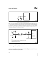
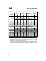
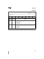
1
27280301.qxd 7/31/96 12:12 PM Page 1 80296SA Microcontroller User’s Manual We Value Your Opinion Dear Intel Customer: Your feedback will help us provide the information you need to design systems incorporating the 80296SA microcontroller. Your responses will guide us in developing other manuals and new versions of this one. Does the manual contain the information that you need? If not, what’s missing? What do you like the most about this manual? What do you like the least about this manual? How would you rate the overall quality of this manual? ___excellent ___very good ___good ___fair Name Title Company Address City, State or Country Zip or Postal Code Phone Fax Intel products used Type of application Please fax this form to (602)554-7674 or mail it to Intel Corporation SPG Tech Pubs, Mail Stop CH6-224 5000 W. Chandler Blvd. Chandler, AZ 85226 or send e-mail to [email protected] Thank you. 80296SA Microcontroller User’s Manual August 2004 Order Number 272803-002 Information in this document is provided in connection with Intel products. No license, express or implied, by estoppel or otherwise, to any intellectual property rights is granted by this document. Except as provided in Intel’s Terms and Conditions of Sale for such products, Intel assumes no liability whatsoever, and Intel disclaims any express or implied warranty, relating to sale and/or use of Intel products including liability or warranties relating to fitness for a particular purpose, merchantability, or infringement of any patent, copyright or other intellectual property right. Intel products are not intended for use in medical, life saving, or life sustaining applications. Intel retains the right to make changes to specifications and product descriptions at any time, without notice. Contact your local Intel sales office or your distributor to obtain the latest specifications and before placing your product order. *Third-party brands and names are the property of their respective owners. Copies of documents which have an ordering number and are referenced in this document, or other Intel literature, may be obtained from: Intel Corporation P.O. Box 7641 Mt. Prospect, IL 60056-7641 or call 1-800-879-4683 Copyright © INTEL CORPORATION, 1996 CONTENTS CHAPTER 1 GUIDE TO THIS MANUAL 1.1 MANUAL CONTENTS ................................................................................................... 1-1 1.2 NOTATIONAL CONVENTIONS AND TERMINOLOGY ................................................ 1-3 1.3 RELATED DOCUMENTS .............................................................................................. 1-6 1.4 APPLICATION SUPPORT SERVICES.......................................................................... 1-7 1.4.1 World Wide Web .......................................................................................................1-7 CHAPTER 2 ARCHITECTURAL OVERVIEW 2.1 TYPICAL APPLICATIONS............................................................................................. 2-1 2.2 FUNCTIONAL OVERVIEW............................................................................................ 2-3 2.2.1 Core ..........................................................................................................................2-3 2.2.1.1 CPU ......................................................................................................................2-4 2.2.1.2 Register File .........................................................................................................2-5 2.2.2 Execution Unit ...........................................................................................................2-5 2.2.3 Memory Interface Unit .............................................................................................2-6 2.2.4 Bus Controller and Chip-select Unit ..........................................................................2-6 2.3 INTERNAL TIMING........................................................................................................ 2-7 2.3.1 Clock and Power Management Logic .......................................................................2-7 2.3.2 Internal Timing ..........................................................................................................2-8 2.3.2.1 Power Management Options ..............................................................................2-11 2.4 INTERNAL PERIPHERALS ........................................................................................ 2-12 2.4.1 I/O Ports ..................................................................................................................2-12 2.4.2 Serial I/O (SIO) Port ................................................................................................2-12 2.4.3 Event Processor Array (EPA) and Timer/Counters .................................................2-12 2.4.4 Pulse-width Modulator (PWM) ................................................................................2-12 2.4.5 Interrupt Controller ..................................................................................................2-13 2.5 SPECIAL OPERATING MODES ................................................................................. 2-13 2.6 CHIP CONFIGURATION REGISTERS ....................................................................... 2-13 2.7 DESIGN CONSIDERATIONS FOR 80C196NU TO 80296SA CONVERSIONS ......... 2-16 CHAPTER 3 DIGITAL SIGNAL PROCESSING 3.1 DIGITAL SIGNAL PROCESSING OVERVIEW ............................................................. 3-1 3.2 DSP REGISTERS.......................................................................................................... 3-1 3.3 ENHANCED INSTRUCTION SET ................................................................................. 3-2 iii 80296SA USER’S MANUAL 3.3.1 Addition and Subtraction (ADDC and SUBC) Instructions ........................................3-3 3.3.1.1 ADDC Instruction .................................................................................................3-3 3.3.1.2 SUBC Instruction ..................................................................................................3-3 3.3.2 Multiply-Accumulate (MAC) Instructions ...................................................................3-4 3.3.3 Move (MSAC and MVAC) Instructions ......................................................................3-6 3.3.3.1 Move Saturated Integer From Accumulator (MSAC) Instruction ..........................3-6 3.3.3.2 Move Double-word from Accumulator (MVAC) Instruction ...................................3-8 3.3.4 Repeat (RPT, RPTI, RPTxxx, RPTIxxx) Instructions ................................................3-8 3.3.4.1 Repeat Next (RPT) Instruction .............................................................................3-8 3.3.4.2 Repeat Next Conditional (RPTxxx) Instruction .....................................................3-9 3.3.4.3 Repeat Next Interruptible (RPTI) Instruction ......................................................3-10 3.3.4.4 Repeat Next Conditional Interruptible (RPTIxxx) Instruction ..............................3-10 3.3.5 Return from Interrupt (RETI) Instruction ..................................................................3-11 3.4 REPEAT COUNTER (RPT_CNT) REGISTER ............................................................ 3-11 3.5 ACCUMULATOR ......................................................................................................... 3-12 3.5.1 Accumulator Register (ACC_0x) .............................................................................3-12 3.5.2 Accumulator Control and Status Register (ACC_STAT) .........................................3-13 3.5.2.1 Saturation Mode (SME) ......................................................................................3-15 3.5.2.2 Fractional Mode .................................................................................................3-15 3.5.3 Accumulator Operation Limit ...................................................................................3-16 3.6 INDEX REGISTERS .................................................................................................... 3-16 3.6.1 Index Pointer (IDX0 and IDX1) Registers ...............................................................3-17 3.6.2 Index Control Byte (ICB0 and ICB1) Registers .......................................................3-17 3.6.3 Index Reference (ICX0 and ICX1) Registers ..........................................................3-18 3.7 APPLICATION EXAMPLE ........................................................................................... 3-19 CHAPTER 4 PROGRAMMING CONSIDERATIONS 4.1 OVERVIEW OF THE INSTRUCTION SET.................................................................... 4-1 4.1.1 BIT Operands ............................................................................................................4-2 4.1.2 BYTE Operands ........................................................................................................4-2 4.1.3 SHORT-INTEGER Operands ....................................................................................4-2 4.1.4 WORD Operands ......................................................................................................4-3 4.1.5 INTEGER Operands .................................................................................................4-3 4.1.6 DOUBLE-WORD Operands ......................................................................................4-3 4.1.7 LONG-INTEGER Operands ......................................................................................4-4 4.1.8 QUAD-WORD Operands ..........................................................................................4-4 4.1.9 Converting Operands ................................................................................................4-4 4.1.10 Conditional Jumps ....................................................................................................4-5 4.1.11 Floating Point Operations .........................................................................................4-5 4.1.12 Extended Instructions ...............................................................................................4-5 4.1.13 Instructions That Were Removed from the 80296SA ................................................4-6 4.1.14 Instructions That Were Enhanced for the 80296SA ..................................................4-6 4.1.15 Instructions That Were Added for the 80296SA .......................................................4-7 iv CONTENTS 4.2 ADDRESSING MODES ................................................................................................. 4-8 4.2.1 Direct Addressing ......................................................................................................4-9 4.2.2 Immediate Addressing ............................................................................................4-10 4.2.3 Indirect Addressing .................................................................................................4-10 4.2.3.1 Extended Indirect Addressing ............................................................................4-10 4.2.3.2 Indirect Addressing with Autoincrement .............................................................4-10 4.2.3.3 Extended Indirect Addressing with Autoincrement .............................................4-11 4.2.3.4 Indirect Addressing with the Stack Pointer .........................................................4-11 4.2.4 Indexed Addressing ................................................................................................4-11 4.2.4.1 Short-indexed Addressing ..................................................................................4-12 4.2.4.2 Long-indexed Addressing ..................................................................................4-12 4.2.4.3 Extended Indexed Addressing ...........................................................................4-12 4.2.4.4 Zero-indexed Addressing ...................................................................................4-13 4.2.4.5 Extended Zero-indexed Addressing ...................................................................4-13 4.3 CONSIDERATIONS FOR CROSSING PAGE BOUNDARIES .................................... 4-13 4.4 SOFTWARE PROTECTION FEATURES AND GUIDELINES .................................... 4-13 CHAPTER 5 MEMORY PARTITIONS 5.1 MEMORY MAP OVERVIEW.......................................................................................... 5-1 5.2 MEMORY PARTITIONS ................................................................................................ 5-4 5.2.1 External Memory .......................................................................................................5-5 5.2.2 Program and Special-purpose Memory ....................................................................5-5 5.2.2.1 Program Memory in Page FFH ............................................................................5-5 5.2.2.2 Special-purpose Memory .....................................................................................5-6 5.2.2.3 Reserved Memory Locations ...............................................................................5-6 5.2.2.4 Interrupt Vectors ...................................................................................................5-6 5.2.2.5 Chip Configuration Bytes .....................................................................................5-6 5.2.3 Internal RAM (Code RAM) ........................................................................................5-7 5.2.4 Peripheral Special-function Registers (SFRs) ...........................................................5-7 5.2.5 Register File ............................................................................................................5-10 5.2.5.1 General-purpose Register RAM .........................................................................5-11 5.2.5.2 Stack Pointer (SP) ..............................................................................................5-11 5.2.5.3 CPU Special-function Registers (SFRs) .............................................................5-12 5.3 WINDOWING............................................................................................................... 5-13 5.3.1 Selecting a Window ................................................................................................5-14 5.3.2 Addressing a Location Through a Window .............................................................5-18 5.3.2.1 32-byte Windowing Example ..............................................................................5-18 5.3.2.2 64-byte Windowing Example ..............................................................................5-19 5.3.2.3 128-byte Windowing Example ............................................................................5-19 5.3.2.4 Using the Linker Locator to Set Up a Window ....................................................5-19 5.3.3 Windowing and Addressing Modes .........................................................................5-21 5.4 FETCHING CODE AND DATA IN THE 1-MBYTE AND 64-KBYTE MODES.............. 5-22 v 80296SA USER’S MANUAL CHAPTER 6 INTERRUPTS 6.1 OVERVIEW OF THE INTERRUPT CONTROL CIRCUITRY......................................... 6-1 6.2 INTERRUPT SIGNALS AND REGISTERS ................................................................... 6-4 6.3 INTERRUPT SOURCES, PRIORITIES, AND VECTOR ADDRESSES ........................ 6-5 6.3.1 Reassigning Vector Addresses .................................................................................6-9 6.3.2 Special Interrupts ....................................................................................................6-10 6.3.2.1 Unimplemented Opcode ....................................................................................6-10 6.3.2.2 Software Trap .....................................................................................................6-10 6.3.2.3 NMI .....................................................................................................................6-10 6.3.3 External Interrupt Signals ........................................................................................6-11 6.3.4 Shared Interrupt Requests ......................................................................................6-11 6.4 INTERRUPT LATENCY............................................................................................... 6-12 6.4.1 Situations that Increase Interrupt Latency ..............................................................6-12 6.4.2 Calculating Latency .................................................................................................6-12 6.4.2.1 Worst-case Interrupt Latency .............................................................................6-13 6.5 PROGRAMMING THE INTERRUPTS......................................................................... 6-14 6.5.1 Determining the Source of an Interrupt ...................................................................6-16 CHAPTER 7 I/O PORTS 7.1 I/O PORTS OVERVIEW ................................................................................................ 7-1 7.2 CONFIGURING THE PORT PINS................................................................................. 7-3 7.2.1 Configuring Ports 1–4 and EPORT ...........................................................................7-4 7.2.2 Port Configuration Example ......................................................................................7-5 7.3 USING THE SPECIAL-FUNCTION SIGNALS............................................................... 7-6 7.3.1 Address Signals (EPORT) ........................................................................................7-6 7.3.2 Bus-control Signals (Port 2) ......................................................................................7-7 7.3.3 Chip-select Signals (Port 3) ......................................................................................7-8 7.3.4 EPA and Timer Signals (Port 1) ................................................................................7-9 7.3.5 External Interrupt Signals (Ports 2 and 3) .................................................................7-9 7.3.6 PWM Signals (Port 4) .............................................................................................7-10 7.3.7 Serial I/O Port Signals (Ports 1 and 2) ....................................................................7-11 7.4 I/O PORT INTERNAL STRUCTURES......................................................................... 7-11 7.4.1 Internal Structure for the Extended I/O Port (EPORT) ............................................7-11 7.4.2 Internal Structure for Ports 1–4 ...............................................................................7-14 CHAPTER 8 SERIAL I/O (SIO) PORT 8.1 SERIAL I/O (SIO) PORT FUNCTIONAL OVERVIEW ................................................... 8-1 8.2 SERIAL I/O PORT SIGNALS AND REGISTERS .......................................................... 8-3 8.3 SERIAL PORT MODES ................................................................................................. 8-6 8.3.1 Synchronous Mode (Mode 0) ....................................................................................8-6 vi CONTENTS 8.3.2 Asynchronous Modes (Modes 1, 2, and 3) ...............................................................8-7 8.3.2.1 Mode 1 .................................................................................................................8-8 8.3.2.2 Mode 2 .................................................................................................................8-9 8.3.2.3 Mode 3 .................................................................................................................8-9 8.3.2.4 Multiprocessor Communications ..........................................................................8-9 8.4 PROGRAMMING THE SERIAL PORT ........................................................................ 8-10 8.4.1 Configuring the Serial Port Pins ..............................................................................8-10 8.4.2 Programming the Control Register ..........................................................................8-10 8.4.3 Programming the Baud Rate and Clock Source .....................................................8-13 8.4.4 Enabling the Serial Port Interrupts ..........................................................................8-16 8.4.5 Determining Serial Port Status ................................................................................8-16 CHAPTER 9 PULSE-WIDTH MODULATOR 9.1 PWM FUNCTIONAL OVERVIEW.................................................................................. 9-1 9.2 PWM SIGNALS AND REGISTERS ............................................................................... 9-2 9.3 PWM OPERATION ........................................................................................................ 9-4 9.4 PWM PERIPHERAL DISABLE CONTROL.................................................................... 9-5 9.5 PROGRAMMING THE FREQUENCY AND PERIOD.................................................... 9-5 9.6 PROGRAMMING THE DUTY CYCLE ........................................................................... 9-7 9.6.1 Sample Calculations .................................................................................................9-9 9.6.2 Enabling the PWM Outputs .......................................................................................9-9 9.6.3 Generating Analog Outputs ......................................................................................9-9 CHAPTER 10 EVENT PROCESSOR ARRAY (EPA) 10.1 EPA FUNCTIONAL OVERVIEW ................................................................................. 10-1 10.2 EPA AND TIMER/COUNTER SIGNALS AND REGISTERS ....................................... 10-2 10.3 TIMER/COUNTER FUNCTIONAL OVERVIEW........................................................... 10-4 10.3.1 Cascade Mode (Timer 2 Only) ................................................................................10-6 10.3.2 Quadrature Clocking Modes ...................................................................................10-6 10.4 EPA CHANNEL FUNCTIONAL OVERVIEW ............................................................... 10-8 10.4.1 Operating in Capture Mode .....................................................................................10-9 10.4.1.1 EPA Overruns ..................................................................................................10-11 10.4.1.2 Preventing EPA Overruns ................................................................................10-12 10.4.2 Operating in Compare Mode .................................................................................10-12 10.4.2.1 Generating a Low-speed PWM Output ............................................................10-12 10.4.2.2 Generating the High-speed PWM Output ........................................................10-13 10.5 PROGRAMMING THE EPA AND TIMER/COUNTERS............................................. 10-14 10.5.1 Configuring the EPA and Timer/Counter Signals ..................................................10-14 10.5.2 Programming the Timers .......................................................................................10-14 10.5.3 Programming the Capture/Compare Channels .....................................................10-18 10.6 ENABLING THE EPA INTERRUPTS ........................................................................ 10-23 vii 80296SA USER’S MANUAL 10.7 DETERMINING EVENT STATUS.............................................................................. 10-25 CHAPTER 11 MINIMUM HARDWARE CONSIDERATIONS 11.1 MINIMUM CONNECTIONS ......................................................................................... 11-1 11.1.1 Unused Inputs .........................................................................................................11-2 11.1.2 I/O Port Pin Connections ........................................................................................11-2 11.2 APPLYING AND REMOVING POWER ....................................................................... 11-3 11.3 NOISE PROTECTION TIPS ........................................................................................ 11-4 11.4 THE ON-CHIP OSCILLATOR CIRCUITRY ................................................................. 11-5 11.5 USING AN EXTERNAL CLOCK SOURCE.................................................................. 11-6 11.6 RESETTING THE DEVICE.......................................................................................... 11-7 11.6.1 Generating an External Reset .................................................................................11-9 11.6.2 Issuing the Reset (RST) Instruction ......................................................................11-10 11.6.3 Issuing an Illegal IDLPD Key Operand .................................................................11-11 CHAPTER 12 SPECIAL OPERATING MODES 12.1 SPECIAL OPERATING MODE SIGNALS AND REGISTERS..................................... 12-1 12.2 REDUCING POWER CONSUMPTION ....................................................................... 12-4 12.3 IDLE MODE ................................................................................................................. 12-5 12.4 STANDBY MODE ........................................................................................................ 12-6 12.4.1 Enabling and Disabling Standby Mode ...................................................................12-6 12.4.2 Entering Standby Mode ..........................................................................................12-6 12.4.3 Exiting Standby Mode .............................................................................................12-7 12.5 POWERDOWN MODE ................................................................................................ 12-7 12.5.1 Enabling and Disabling Powerdown Mode ..............................................................12-7 12.5.2 Entering Powerdown Mode .....................................................................................12-8 12.5.3 Exiting Powerdown Mode .......................................................................................12-8 12.5.3.1 Generating a Hardware Reset ...........................................................................12-8 12.5.3.2 Asserting an External Interrupt Signal ................................................................12-8 12.5.3.3 Selecting C1 .....................................................................................................12-11 12.6 ONCE MODE............................................................................................................. 12-12 12.7 ADDITIONAL POWER CONSERVATION FEATURES............................................. 12-13 12.8 RESERVED TEST MODES....................................................................................... 12-13 CHAPTER 13 INTERFACING WITH EXTERNAL MEMORY 13.1 INTERNAL AND EXTERNAL ADDRESSES ............................................................... 13-1 13.2 EXTERNAL MEMORY INTERFACE SIGNALS AND REGISTERS ............................ 13-2 13.3 THE CHIP-SELECT UNIT............................................................................................ 13-8 13.3.1 Defining Chip-select Address Ranges ....................................................................13-9 13.3.2 Controlling Bus Parameters ..................................................................................13-11 viii CONTENTS 13.3.3 Chip-select Unit Initial Conditions .........................................................................13-14 13.3.4 Programming the Chip-select Registers ...............................................................13-14 13.3.5 Example of a Chip-select Setup ............................................................................13-15 13.3.6 Example of a Chip-select Setup Using the Remap Feature ..................................13-16 13.4 CHIP CONFIGURATION REGISTERS AND CHIP CONFIGURATION BYTES ....... 13-17 13.5 BUS WIDTH AND MULTIPLEXING........................................................................... 13-21 13.5.1 A 16-bit Example System ......................................................................................13-24 13.5.2 16-bit Bus Timings ................................................................................................13-25 13.5.3 8-bit Bus Timings ..................................................................................................13-27 13.5.4 Comparison of Multiplexed and Demultiplexed Buses ..........................................13-29 13.6 WAIT STATES (READY CONTROL)......................................................................... 13-29 13.7 BUS-HOLD PROTOCOL ........................................................................................... 13-32 13.7.1 Enabling the Bus-hold Protocol .............................................................................13-34 13.7.2 Disabling the Bus-hold Protocol ............................................................................13-34 13.7.3 Hold Latency .........................................................................................................13-35 13.7.4 Regaining Bus Control ..........................................................................................13-35 13.8 WRITE-CONTROL MODES ...................................................................................... 13-35 13.9 SYSTEM BUS AC TIMING SPECIFICATIONS ......................................................... 13-38 13.9.1 Deferred Bus-cycle Mode .....................................................................................13-40 13.9.2 Explanation of AC Symbols ..................................................................................13-41 13.9.3 AC Timing Definitions ...........................................................................................13-42 APPENDIX A INSTRUCTION SET REFERENCE APPENDIX B SIGNAL DESCRIPTIONS B.1 FUNCTIONAL GROUPINGS OF SIGNALS ................................................................. B-1 B.2 SIGNAL DESCRIPTIONS............................................................................................. B-3 B.3 DEFAULT CONDITIONS ............................................................................................ B-10 APPENDIX C REGISTERS GLOSSARY INDEX ix 80296SA USER’S MANUAL FIGURES Figure 2-1 2-2 2-3 2-4 2-5 2-6 2-7 2-8 2-9 3-1 3-2 3-3 3-4 3-5 3-6 3-7 3-8 3-9 5-1 5-2 5-3 5-4 5-5 5-6 6-1 6-2 6-3 6-4 6-5 6-6 6-7 6-8 6-9 6-10 6-11 6-12 7-1 7-2 8-1 8-2 8-3 8-4 8-5 8-6 x Page 80296SA Detailed Block Diagram ................................................................................2-2 80296SA Block Diagram ..............................................................................................2-3 Block Diagram of the Core ...........................................................................................2-4 Instruction Pipeline .......................................................................................................2-5 Clock Circuitry ..............................................................................................................2-7 Internal Clock Phases (Assuming PLL is Bypassed)....................................................2-8 Effect of Clock Mode on CLKOUT Frequency............................................................2-10 Chip Configuration 0 (CCR0) Register .......................................................................2-14 Chip Configuration 1 (CCR1) Register .......................................................................2-15 MSAC Instruction Example...........................................................................................3-7 Repeat Counter (RPT_CNT) Register........................................................................3-12 Accumulator (ACC_0x) Register ................................................................................3-13 Accumulator Control and Status (ACC_STAT) Register ............................................3-14 Index Pointer (IDXx) Registers ...................................................................................3-17 Index Control Byte (ICBx) Registers...........................................................................3-18 Index Reference (ICXx) Registers..............................................................................3-19 Application Code Illustration .......................................................................................3-20 FIR Filter Block Diagram ............................................................................................3-21 16-Mbyte Address Space .............................................................................................5-2 Pages FFH and 00H.....................................................................................................5-3 Register File Memory Map .........................................................................................5-10 Windowing ..................................................................................................................5-14 Window Selection (WSR) Register.............................................................................5-15 Window Selection 1 (WSR1) Register........................................................................5-15 Interrupt Structure Block Diagram ................................................................................6-2 Interrupt Service Flow Diagram ....................................................................................6-3 NMI Pending (NMI_PEND) Register ............................................................................6-7 Interrupt Control (INT_CONx) Registers ......................................................................6-8 Interrupt Vector Address (VECT_ADDR) Register .....................................................6-10 External Interrupt Control (EXTINT_CON) Register...................................................6-11 Worst-case Interrupt Response Time.........................................................................6-13 Interrupt Mask (INT_MASK) Register.........................................................................6-15 Interrupt Mask 1 (INT_MASK1) Register....................................................................6-16 Interrupt In-progress (IN_PROGx) Registers .............................................................6-17 Interrupt Pending (INT_PEND) Register ....................................................................6-18 Interrupt Pending 1 (INT_PEND1) Register ...............................................................6-19 EPORT Internal Structure ..........................................................................................7-13 Ports 1–4 Internal Structure .......................................................................................7-15 SIO Block Diagram (Mode 0)........................................................................................8-2 SIO Block Diagram (Mode 1, 2, and 3).........................................................................8-3 Mode 0 Timing..............................................................................................................8-6 Serial Port Frames for Mode 1 .....................................................................................8-8 Serial Port Frames in Mode 2 and 3.............................................................................8-9 Serial Port Control (SP_CON) Register......................................................................8-11 CONTENTS FIGURES Figure 8-7 8-8 9-1 9-2 9-3 9-4 9-5 9-6 10-1 10-2 10-3 10-4 10-5 10-6 10-7 10-8 10-9 10-10 10-11 10-12 10-13 10-14 10-15 10-16 11-1 11-2 11-3 11-4 11-5 11-6 11-7 11-8 11-9 11-10 12-1 12-2 12-3 12-4 13-1 13-2 13-3 13-4 13-5 13-6 Page Serial Port Baud Rate (SP_BAUD) Register ..............................................................8-14 Serial Port Status (SP_STATUS) Register.................................................................8-17 PWM Block Diagram ....................................................................................................9-2 PWM Output Waveforms..............................................................................................9-5 Control (CON_REG0) Register ....................................................................................9-7 PWM Control (PWMx_CONTROL) Registers ..............................................................9-8 D/A Buffer Block Diagram...........................................................................................9-10 PWM to Analog Conversion Circuitry .........................................................................9-10 EPA Block Diagram ....................................................................................................10-2 EPA Timer/Counters ..................................................................................................10-5 Quadrature Mode Interface ........................................................................................10-7 Quadrature Mode Timing and Count ..........................................................................10-8 A Single EPA Capture/Compare Channel ..................................................................10-9 EPA Simplified Input-capture Structure ....................................................................10-10 Valid EPA Input Events ............................................................................................10-10 Timer 1 Control (T1CONTROL) Register .................................................................10-15 Timer 2 Control (T2CONTROL) Register .................................................................10-16 Timer x Time (TIMERx) Registers ............................................................................10-18 EPA Control (EPAx_CON) Registers .......................................................................10-20 EPA Time (EPAx_TIME) Registers ..........................................................................10-23 EPA Interrupt Mask (EPA_MASK) Register .............................................................10-24 Interrupt Mask (INT_MASK) Register.......................................................................10-24 Interrupt Mask 1 (INT_MASK1) Register..................................................................10-25 EPA Interrupt Pending (EPA_PEND) Register.........................................................10-26 Minimum Hardware Connections ...............................................................................11-3 Power and Return Connections .................................................................................11-4 On-chip Oscillator Circuit............................................................................................11-5 External Crystal Connections .....................................................................................11-6 External Clock Connections .......................................................................................11-7 External Clock Drive Waveforms................................................................................11-7 Reset Timing Sequence .............................................................................................11-8 Internal Reset Circuitry ...............................................................................................11-9 Minimum Reset Circuit .............................................................................................11-10 Example of a System Reset Circuit ..........................................................................11-10 Clock Control During Power-saving Modes................................................................12-5 Power-up and Power-down Sequence When Using an External Interrupt.................12-9 External RC Circuit ...................................................................................................12-10 Typical Voltage on the RPD Pin While Exiting Powerdown......................................12-11 Calculation of a Chip-select Output ............................................................................13-8 Address Compare (ADDRCOMx) Registers...............................................................13-9 Address Mask (ADDRMSKx) Registers ...................................................................13-10 Bus Control (BUSCONx) Registers ..........................................................................13-12 Example System for Setting Up Chip-select Outputs ...............................................13-15 Chip Configuration 0 (CCR0) Register .....................................................................13-18 xi 80296SA USER’S MANUAL FIGURES Figure 13-7 13-8 13-9 13-10 13-11 13-12 13-13 13-14 13-15 13-16 13-17 13-18 13-19 13-20 13-21 B-1 B-2 xii Page Chip Configuration 1 (CCR1) Register .....................................................................13-19 Multiplexing and Bus Width Options.........................................................................13-22 Bus Activity for Four Types of Buses........................................................................13-23 16-bit External Devices in Demultiplexed Mode .......................................................13-25 Timings for Multiplexed and Demultiplexed 16-bit Buses.........................................13-26 Timings for Multiplexed and Demultiplexed 8-bit Buses...........................................13-28 READY Timing Diagram — Multiplexed Mode .........................................................13-30 READY Timing Diagram — Demultiplexed Mode ....................................................13-31 HOLD#, HLDA# Timing ............................................................................................13-33 Write-control Signal Waveforms ...............................................................................13-36 Decoding WRL# and WRH#.....................................................................................13-37 A System with 8-bit and 16-bit Buses.......................................................................13-38 Multiplexed System Bus Timing ...............................................................................13-39 Demultiplexed System Bus Timing...........................................................................13-40 Deferred Bus-cycle Mode Timing Diagram...............................................................13-41 80296SA 100-pin SQFP Package ............................................................................... B-2 80296SA 100-pin QFP Package ................................................................................. B-3 CONTENTS TABLES Table 1-1 1-2 1-3 1-4 2-1 2-2 2-3 3-1 3-2 3-3 3-4 3-5 3-6 3-7 3-8 4-1 4-2 4-3 4-4 5-1 5-2 5-3 5-4 5-5 5-6 5-7 5-8 5-9 5-10 6-1 6-2 6-3 6-4 6-5 7-1 7-2 7-3 7-4 7-5 7-6 7-7 7-8 7-9 7-10 Page Handbooks and Product Information ............................................................................1-6 Application Notes .........................................................................................................1-7 MCS® 96 Microcontroller Datasheets...........................................................................1-7 Intel Application Support Services................................................................................1-8 Features of the 80296SA .............................................................................................2-1 State Times at Various Frequencies ............................................................................2-9 Relationships Between Input Frequency, Clock Multiplier, and State Times ...............2-9 DSP Control and Status Registers ...............................................................................3-1 Enhanced Instruction Set for the 80296SA ..................................................................3-3 Multiply-Accumulate Instruction Bit Definition...............................................................3-4 Multiply-Accumulate Instruction Set .............................................................................3-5 Accumulator Usage Examples .....................................................................................3-6 Repeat Instructions ......................................................................................................3-8 Repeat Instruction Exit Conditions ...............................................................................3-9 Effect of SME and FME Bit Combinations..................................................................3-15 Data Type Definitions ...................................................................................................4-1 Equivalent Data Types for Assembly and C Programming Languages........................4-2 Converting Data Types.................................................................................................4-4 Definition of Temporary Registers ................................................................................4-9 80296SA Memory Map.................................................................................................5-4 80296SA Special-purpose Memory Addresses............................................................5-6 Peripheral SFRs ...........................................................................................................5-8 Register File Memory Addresses ...............................................................................5-11 80296SA CPU SFRs ..................................................................................................5-13 Selecting a Window of Peripheral SFRs.....................................................................5-16 Selecting a Window of the Upper Register File ..........................................................5-16 Selecting a Window of the Internal Code RAM ..........................................................5-17 Selecting a Window of External Memory....................................................................5-17 Windowed Base Addresses .......................................................................................5-18 Interrupt Signals ...........................................................................................................6-4 Interrupt Registers ........................................................................................................6-4 Interrupt Sources, Vectors, and Priorities.....................................................................6-6 INT_CONx Address and Reset States .........................................................................6-9 Programming the Interrupts........................................................................................6-14 Microcontroller I/O Ports...............................................................................................7-1 Microcontroller Port Signals..........................................................................................7-2 Port Control and Status Registers ................................................................................7-3 Control Register Values for Each Configuration...........................................................7-5 Port Configuration Example .........................................................................................7-5 Port Pin States After Reset and After Example Code Execution..................................7-6 Address Signals ...........................................................................................................7-6 Bus-control Signals ......................................................................................................7-7 Chip-select Signals.......................................................................................................7-8 EPA and Timer Signals ................................................................................................7-9 xiii 80296SA USER’S MANUAL TABLES Table 7-11 7-12 7-13 8-1 8-2 8-3 8-4 8-5 9-1 9-2 9-3 9-4 10-1 10-2 10-3 10-4 10-5 11-1 12-1 12-2 12-3 13-1 13-2 13-3 13-4 13-5 13-6 13-7 13-8 13-9 13-10 13-11 13-12 13-13 A-1 A-1 A-2 A-3 A-4 A-5 A-6 A-7 A-8 A-9 xiv Page External Interrupt Signals ...........................................................................................7-10 PWM Signals..............................................................................................................7-10 SIO Signals ................................................................................................................7-11 Serial Port Signals ........................................................................................................8-4 Serial Port Control and Status Registers......................................................................8-4 Port Register Settings for the SIO Signals .................................................................8-10 SP_BAUD Values When Using the Internal Clock at 25 MHz....................................8-15 SP_BAUD Values When Using the Internal Clock at 50 MHz....................................8-15 PWM Signals................................................................................................................9-2 PWM Control and Status Registers..............................................................................9-3 PWM Output Frequencies ............................................................................................9-6 PWM Output Alternate Functions .................................................................................9-9 EPA and Timer/Counter Signals.................................................................................10-2 EPA Control and Status Registers .............................................................................10-3 Quadrature Mode Truth Table ....................................................................................10-7 Action Taken When a Valid Edge Occurs ................................................................10-11 Example EPA Control Register Settings ..................................................................10-19 Minimum Required Signals.........................................................................................11-1 Operating Mode Control Signals ................................................................................12-1 Operating Mode Control and Status Registers...........................................................12-3 80296SA Clock Modes .............................................................................................12-14 Example of Internal and External Addresses .............................................................13-1 Bus-control Signals ....................................................................................................13-2 External Memory Interface Registers .........................................................................13-5 Base Addresses for Several Sizes of the Address Range .......................................13-11 BUSCONx Registers for the Example System .........................................................13-15 Results for the Chip-select Example ........................................................................13-16 READY Signal Timing Definitions.............................................................................13-31 HOLD#, HLDA# Timing Definitions ..........................................................................13-33 Maximum Hold Latency ............................................................................................13-35 Write Signals for Standard and Write Strobe Modes................................................13-36 AC Timing Symbol Definitions ..................................................................................13-42 External Memory Systems Must Meet These Specifications....................................13-42 The Microcontroller Meets These Specifications......................................................13-43 Opcode Map (Left Half) ............................................................................................... A-2 Opcode Map (Right Half)............................................................................................. A-3 Processor Status Word (PSW) Flags .......................................................................... A-4 Effect of PSW Flags or Specified Conditions on Conditional Jump Instructions ......... A-5 PSW Flag Setting Symbols ......................................................................................... A-5 Operand Variables ...................................................................................................... A-6 Instruction Set ............................................................................................................. A-7 Instruction Opcodes .................................................................................................. A-57 Number of Bytes for Each Instruction and Hexadecimal Opcodes............................ A-64 Instruction Execution Times (in State Times) ............................................................ A-72 CONTENTS TABLES Table B-1 B-2 B-3 B-4 B-5 C-1 C-2 C-3 C-4 C-5 C-6 C-7 C-8 C-9 C-10 C-11 C-12 C-13 C-14 C-15 C-16 C-17 Page 80296SA Signals Arranged by Function ..................................................................... B-1 Description of Columns of Table B-3........................................................................... B-4 Signal Descriptions...................................................................................................... B-4 Definition of Status Symbols ..................................................................................... B-11 80296SA Default Signal Conditions .......................................................................... B-11 Modules and Related Registes ................................................................................... C-1 Register Name, Address, and Reset State.................................................................. C-2 Effect of SME and FME Bit Combinations................................................................... C-8 ADDRCOMx Addresses and Reset States.................................................................. C-9 ADDRMSKx Addresses and Reset States ................................................................ C-10 BUSCONx Addresses and Reset States................................................................... C-12 EPAx_CON Addresses and Reset States ................................................................. C-26 EPAx_TIME Addresses and Reset States ................................................................ C-27 INT_CONx Address and Reset States ...................................................................... C-34 Px_DIR Addresses and Reset States........................................................................ C-41 Px_MODE Addresses and Reset States ................................................................... C-42 Special-function Signals for Ports 1–4....................................................................... C-43 Px_PIN Addresses and Reset States........................................................................ C-44 Px_REG Addresses and Reset States...................................................................... C-46 PWMx_CONTROL Addresses and Reset States...................................................... C-49 WSR Settings and Direct Addresses for Windowable SFRs ..................................... C-63 WSR1 Settings and Direct Addresses for Windowable SFRs ................................... C-67 xv 1 Guide to This Manual CHAPTER 1 GUIDE TO THIS MANUAL This manual describes the 80296SA embedded microcontroller. It is intended for use by both software and hardware designers familiar with the principles of microcontrollers. This chapter describes what you’ll find in this manual, lists other documents that may be useful, and explains how to access the support services we provide to help you complete your design. 1.1 MANUAL CONTENTS This manual contains several chapters and appendixes, a glossary, and an index. This chapter, Chapter 1, provides an overview of the manual. This section summarizes the contents of the remaining chapters and appendixes. The remainder of this chapter describes notational conventions and terminology used throughout the manual, provides references to related documentation, describes customer support services, and explains how to access information and assistance. Chapter 2 — Architectural Overview — provides an overview of the device hardware. It describes the core, internal timing, internal peripherals, and special operating modes. It also describes the chip configuration bytes (CCBs) and the chip configuration registers (CCRs), which control many aspects of the microcontroller’s operation. Chapter 3 — Digital Signal Processing — describes the advanced mathematical features of the 80296SA that enable it to perform digital signal processing functions. The 80296SA incorporates enhanced instructions for multiplication, shifting, and multiply-accumulate operations. It also has a dedicated 32-bit barrel shifter for manipulating data and a 40-bit accumulator register for storing the results. The instructions and accumulator support signed and unsigned integers as well as signed fractional data. Chapter 4 — Programming Considerations — provides an overview of the instruction set, describes general standards and conventions, and defines the operand types and addressing modes supported by the MCS® 96 microcontroller family. (For additional information about the instruction set, see Appendix A.) Chapter 5 — Memory Partitions — describes the addressable memory space of the device. It describes the memory partitions, explains how to use windows to increase the amount of memory that can be accessed with direct addressing, and lists all special-function registers (SFRs) with their addresses. Chapter 6 — Interrupts — describes the interrupt controller and programmable priority scheme. It also explains interrupt programming and control. 1-1 80296SA USER’S MANUAL Chapter 7 — I/O Ports — describes the input/output ports and explains how to configure the pins for general-purpose input/output or for special functions. Chapter 8 — Serial I/O (SIO) Port — describes the asynchronous/synchronous serial I/O (SIO) port and explains how to program it. Chapter 9 — Pulse-width Modulator — provides a functional overview of the pulse width modulator (PWM) modules, describes how to program them, and provides sample circuitry for converting the PWM outputs to analog signals. Chapter 10 — Event Processor Array (EPA) — describes the event processor array, a timer/counter-based, high-speed input/output unit. It describes the timer/counters and explains how to program the EPA and how to use the EPA to produce pulse-width modulated (PWM) outputs. Chapter 11 — Minimum Hardware Considerations — describes options for providing the basic requirements for device operation within a system, discusses other hardware considerations, and describes device reset options. Chapter 12 — Special Operating Modes — provides an overview of the idle, powerdown, standby, and on-circuit emulation (ONCE) modes and describes how to enter and exit each mode. Chapter 13 — Interfacing with External Memory — lists the signals and registers used for interfacing to external devices. It discusses the bus width and memory configurations, the bushold protocol, write-control modes, and internal wait states and ready control. Finally, it provides timing information for the system bus. Appendix A — Instruction Set Reference — provides reference information for the instruction set. It describes each instruction; defines the processor status word (PSW) flags; shows the relationships between instructions and PSW flags; and lists hexadecimal opcodes, instruction lengths, and execution times. (For additional information about the instruction set, see Chapter 4, “Programming Considerations.”) Appendix B — Signal Descriptions — provides reference information for the device pins, including descriptions of the pin functions, reset status of the I/O and control pins, and package pin assignments. Appendix C — Registers — provides a compilation of all special-function registers (SFRs), arranged alphabetically by register mnemonic. It also includes tables that list the windowed direct addresses for all SFRs in each possible window. Glossary — defines terms with special meaning used throughout this manual. Index — lists key topics with page number references. 1-2 GUIDE TO THIS MANUAL 1.2 NOTATIONAL CONVENTIONS AND TERMINOLOGY The following notations and terminology are used throughout this manual. The Glossary defines other terms with special meanings. # The pound symbol (#) has either of two meanings, depending on the context. When used with a signal name, the symbol means that the signal is active low. When used in an instruction, the symbol prefixes an immediate value in immediate addressing mode. addresses In this manual, both internal and external addresses use the number of hexadecimal digits that correspond with the number of available address bits. For example, the highest possible internal address is shown as FFFFFFH, while the highest possible external address is shown as FFFFFH. When writing code, use the appropriate address conventions for the software tool you are using. (In general, assemblers require a zero preceding an alphabetic hexadecimal character and an “H” following any hexadecimal value, so FFFFFFH must be written as 0FFFFFFH. ANSI ‘C’ compilers require a zero plus an “x” preceding a hexadecimal value, so FFFFFFH must be written as 0xFFFFFF.) Consult the manual for your assembler or compiler to determine its specific requirements. assert and deassert The terms assert and deassert refer to the act of making a signal active (enabled) and inactive (disabled), respectively. The active polarity (low or high) is defined by the signal name. Active-low signals are designated by a pound symbol (#) suffix; active-high signals have no suffix. To assert RD# is to drive it low; to assert ALE is to drive it high; to deassert RD# is to drive it high; to deassert ALE is to drive it low. clear and set The terms clear and set refer to the value of a bit or the act of giving it a value. If a bit is clear, its value is “0”; clearing a bit gives it a “0” value. If a bit is set, its value is “1”; setting a bit gives it a “1” value. f Lowercase “f” represents the internal operating frequency. See “Internal Timing” on page 2-8 for details. instructions Instruction mnemonics are shown in upper case to avoid confusion. In general, you may use either upper case or lower case when programming. Consult the manual for your assembler or compiler to determine its specific requirements. 1-3 80296SA USER’S MANUAL italics Italics identify variables and introduce new terminology. The context in which italics are used distinguishes between the two possible meanings. Variables in registers and signal names are commonly represented by x and y, where x represents the first variable and y represents the second variable. For example, in register Px_MODE.y, x represents the variable that identifies the specific port associated with the register, and y represents the register bit variable (7:0 or 15:0). Variables must be replaced with the correct values when configuring or programming registers or identifying signals. numbers Hexadecimal numbers are represented by a string of hexadecimal digits followed by the character H. Decimal and binary numbers are represented by their customary notations. (That is, 255 is a decimal number and 1111 1111 is a binary number. In some cases, the letter B is appended to binary numbers for clarity.) register bits Bit locations are indexed by 7:0 (or 15:0), where bit 0 is the leastsignificant bit and bit 7 (or 15) is the most-significant bit. An individual bit is represented by the register name, followed by a period and the bit number. For example, WSR.7 is bit 7 of the window selection register. In some discussions, bit names are used. register names Register mnemonics are shown in upper case. For example, TIMER2 is the timer 2 register; timer 2 is the timer. A register name containing a lowercase italic character represents more than one register. For example, the x in Px_REG indicates that the register name refers to any of the port data registers. reserved bits Certain bits are described as reserved bits. In illustrations, reserved bits are indicated with a dash (—). These bits are not used in this device, but they may be used in future implementations. To help ensure that a current software design is compatible with future implementations, reserved bits should be cleared (given a value of “0”) or left in their default states, unless otherwise noted. Do not rely on the values of reserved bits; consider them undefined. reserved registers Certain special-function register (SFR) locations are described as reserved. These locations are not used in this microcontroller, but they may be used in future implementations. To help ensure that a current software design is compatible with future implementations, do not use these locations. 1-4 GUIDE TO THIS MANUAL signal names Signal names are shown in upper case. When several signals share a common name, an individual signal is represented by the signal name followed by a number. For example, the EPA signals are named EPA0, EPA1, EPA2, etc. Port pins are represented by the port abbreviation, a period, and the pin number (e.g., P2.0, P2.1); a range of pins is represented by Px.y:z (e.g., P2.4:0 represents five port pins: P2.4, P2.3, P2.2, P2.1, P2.0). A pound symbol (#) appended to a signal name identifies an active-low signal. t Lowercase “t” represents the internal operating period. See “Internal Timing” on page 2-8 for details. units of measure The following abbreviations are used to represent units of measure: A DCV Kbytes kHz kΩ mA Mbytes MHz ms mW ns pF W V µA µF µs µW amps, amperes direct current volts kilobytes kilohertz kilo-ohms milliamps, milliamperes megabytes megahertz milliseconds milliwatts nanoseconds picofarads watts volts microamps, microamperes microfarads microseconds microwatts x Lowercase x (italic) represents a variable. Variables must be replaced with the correct values when configuring or programming registers or identifying signals. X Uppercase X (no italics) represents an unknown value or an irrelevant (“don’t care”) state or condition. The value may be either binary or hexadecimal, depending on the context. For example, 2XAFH (hex) indicates that bits 11:8 are unknown; 10XXB (binary) indicates that the two least-significant bits are unknown. y Lowercase y (italic) represents a variable. Variables must be replaced with the correct values when configuring or programming registers or identifying signals. 1-5 80296SA USER’S MANUAL 1.3 RELATED DOCUMENTS The tables in this section list additional documents that you may find useful in designing systems incorporating MCS 96 microcontrollers. These are not comprehensive lists, but are a representative sample of relevant documents. For a complete list of available printed documents, please order the literature catalog (order number 210621). To order documents, please call the Intel literature center for your area (see Table 1-4 on page 1-8). Table 1-1. Handbooks and Product Information Title and Description Order Number Intel Embedded Quick Reference Guide Solutions for Embedded Applications Guide Data on Demand fact sheet Data on Demand annual subscription (6 issues; Windows* version) Complete set of Intel handbooks on CD-ROM. Handbook Set — handbooks and product overview Intel’s product line handbooks containing datasheets, application notes, article reprints and other design information on microprocessors, peripherals, embedded controllers, memory components, single-board computers, microcommunications, software development tools, and operating systems. Embedded Microcontrollers † Datasheets and architecture descriptions for Intel’s three industry-standard microcontrollers, the MCS 48, MCS 51, and MCS 96 microcontrollers. Peripheral Components † Comprehensive information on Intel’s peripheral components, including datasheets, application notes, and technical briefs. Flash Memory (2 volume set) † A collection of datasheets and application notes devoted to techniques and information to help design semiconductor memory into an application or system. Packaging † Detailed information on the manufacturing, applications, and attributes of a variety of semiconductor packages. Automotive Products Application notes and article reprints on topics including the MCS 51 and MCS 96 microcontrollers. Documents in this handbook discuss hardware and software implementations and present helpful design techniques. Embedded Applications (1995/96) Datasheets, architecture descriptions, and application notes on topics including flash memory devices, networking chips, and MCS 51 and MCS 96 microcontrollers. Documents in this handbook discuss hardware and software implementations and present helpful design techniques. Development Tools Handbook Information on third-party hardware and software tools that support Intel’s embedded microcontrollers. † Included in handbook set (order number 231003) 272439 1-6 240691 240952 240897 231003 270646 296467 210830 240800 231792 270648 272326 GUIDE TO THIS MANUAL Table 1-2. Application Notes Title AP-125, Designing Microcontroller Systems for Electrically Noisy Environments Order Number ††† 210313 AP-155, Oscillators for Microcontrollers ††† 230659 AP-406, MCS® 96 Analog Acquisition Primer ††† 270365 AP-445, 8XC196KR Peripherals: A User’s Point of View † 270873 AP-477, Low Voltage Embedded Design †† 272324 AP-715, Interfacing an I2C Serial EEPROM to an MCS® 96 Microcontroller 272680 AP-717, Migration from the 8XC196Nx to the 80296SA 272730 † Included in Automotive Products handbook (order number 231792) †† Included in Embedded Applications handbook (order number 270648) ††† Included in Automotive Products and Embedded Applications handbooks Table 1-3. MCS® 96 Microcontroller Datasheets Title 8XC196NP Commercial CHMOS 16-Bit Microcontroller † 80C196NU Commercial CHMOS 16-Bit Microcontroller † 80296SA Commercial CHMOS 16-Bit Microcontroller † Included in Embedded Microcontrollers handbook (order number 270646) 1.4 Order Number 272459 272644 272748 APPLICATION SUPPORT SERVICES You can get up-to-date technical information from the World Wide Web . In the U.S. and Canada, technical support representatives are available to answer your questions between 5 a.m. and 5 p.m. Pacific Standard Time (PST). Outside the U.S. and Canada, please contact your local distributor. You can order product literature from Intel literature centers and sales offices. 1.4.1 World Wide Web We offer a variety of technical and product information through the World Wide Web (URL: http://www.intel.com/design/mcs96). Also visit Intel’s Web site for financials, history, and news. 1-7 80296SA USER’S MANUAL This Page Left Intentionally Blank 1-8 GUIDE TO THIS MANUAL This Page Left Intentionally Blank 1-9 80296SA USER’S MANUAL This Page Left Intentionally Blank 1-10 2 Architectural Overview CHAPTER 2 ARCHITECTURAL OVERVIEW The 16-bit 80296SA CHMOS microcontroller is designed to handle high-speed calculations and fast input/output (I/O) operations. The core of the 80296SA differs from that of earlier MCS® 96 microcontroller cores. It was designed to provide a significant performance increase while maintaining object-code compatibility with earlier MCS 96 microcontrollers. Major contributors to the performance increase are the 80296SA’s pipelined architecture, improved math performance, and new hardware and instructions to support embedded digital signal processing applications. The 80296SA is pin-compatible with the 8XC196NP and 80C196NU, allowing you to place an 80296SA into a socket designed for the 8XC196NP or 80C196NU and improve your system’s performance. 2.1 TYPICAL APPLICATIONS MCS 96 microcontrollers are typically used for high-speed event control systems. Commercial applications include modems, motor-control systems, printers, photocopiers, air conditioner control systems, disk drives, and medical instruments. Automotive customers use MCS 96 microcontrollers in engine-control systems, airbags, suspension systems, and antilock braking systems (ABS). The 80296SA is especially well suited to applications that benefit from its fast instruction execution times and digital signal processing functions, such as mass storage applications. Table 2-1 lists the features of the 80296SA, and Figure 2-1 shows a detailed block diagram. Table 2-1. Features of the 80296SA Device Pins Register RAM (Note 1) Code/Data RAM I/O Pins (Note 2) EPA Pins SIO Ports PWM Channels Chipselect Pins External Interrupt Pins 80296SA 100 512 bytes 2 Kbytes 64 4 1 3 6 4 NOTES: 1. Register RAM amount includes the 24 bytes allocated to core special-function registers (SFRs) and the stack pointer. 2. I/O pins include address, data, and bus control pins and 32 I/O port pins. 2-1 80296SA USER’S MANUAL Code/Data RAM (2 Kbytes) Port 3 Memory Addr Bus (24) SIO Memory Data Bus (16) Chip-select Unit Bus Control Signals A19:16 Baudrate Generator Port 2 Bus Controller Peripheral Bus Interface A15:0 AD15:0 PWM Aligner Queue Port 4 Instruction Sequencer Register File (3-port RAM) Memory Interface Unit Destination Addr (24) Destination Data (16) Peripheral Addr Bus (8) ALU EPA Peripheral Data Bus (16) Source 2 Addr (24) Source 2 Data (16) Memory Addr Bus (24) Source 1 Addr (24) Source 1 Data (16) Memory Data Bus (16) Interrupt Controller Timer 1 Timer 2 Port 1 A3175-02 Figure 2-1. 80296SA Detailed Block Diagram 2-2 ARCHITECTURAL OVERVIEW 2.2 FUNCTIONAL OVERVIEW Figure 2-2 is a simplified block diagram that shows the major blocks within the microcontroller. The shaded area of Figure 2-2 encompasses the core, clock and power management logic, internal code/data RAM, the bus controller, and the chip-select unit. All communication among these blocks takes place through the 24-bit memory address bus. Outside the shaded area are the internal peripherals: general-purpose input/output (I/O) ports, serial input/output (SIO) port, pulsewidth modulator (PWM), event processor array (EPA), and programmable interrupt controller. The peripheral interface communicates through the 8-bit peripheral address bus. Bus Controller Core Code/Data RAM Clock and Power Mgmt. Chip-select Unit Peripheral Interface I/O SIO PWM EPA Interrupt Controller A3182-01 Figure 2-2. 80296SA Block Diagram 2.2.1 Core The core of the 80296SA (Figure 2-3) consists of the central processing unit (CPU) and memory interface unit. The CPU contains the aligner and instruction sequencer, the execution unit, and the register file. A 24-bit memory address bus connects the CPU and memory interface unit; an extension of this bus connects the memory interface unit to the bus controller. An 8-bit peripheral address bus allows communication with the interrupt controller and internal peripherals. 2-3 80296SA USER’S MANUAL CPU Aligner and Instruction Sequencer Execution Unit ALU 10-byte Queue Register File Memory Interface Unit Register RAM 32-bit Barrel Shifter Multiply Divide 40-bit Accumulator 24-bit Slave PC 24-bit Master PC Microcode ROM PSW Constants Register Bit-select Register Stack Pointer Loop Counter CPU SFRs A2848-01 Figure 2-3. Block Diagram of the Core 2.2.1.1 CPU The 80296SA implements a pipelined architecture. The pipelined microcode engine controls the CPU, instructing the execution unit to perform operations using bytes, words, or double-words from either the 256-byte lower register file or through a window that directly accesses higher memory. (See Chapter 5, “Memory Partitions,” for more information about the register file and windowing.) In addition, two automatic indexing registers (IDX0 and IDX1) provide indirect access to the entire 16-Mbyte internal address space. CPU instructions move from the memory interface unit into the queue, then into the instruction sequencer, and finally into the execution pipeline. The aligner and instruction sequencer maintain a steady flow of instructions into the pipeline. The pipeline has four stages: fetch, decode, read-execute, and execute-write. Instructions move sequentially through the pipeline stages, as shown in Figure 2-4. 2-4 ARCHITECTURAL OVERVIEW tion ruc er Instquenc Se ch Fet e od Dec rite e cut Exe dRea te-W cu Exe e Don n ... 5 4 3 2 1 n ... 6 5 4 3 2 1 n ... 7 6 5 4 3 2 1 n ... 8 7 6 5 4 3 2 1 n ... 9 8 7 6 5 4 3 2 1 n . . . 10 9 8 7 6 5 4 3 2, 1 A3061-01 Figure 2-4. Instruction Pipeline 2.2.1.2 Register File The register file is divided into an upper and a lower file. In the lower register file, the lowest 24byte section is allocated to the CPU’s special-function registers (SFRs) and the stack pointer, while the remainder is available as general-purpose register RAM. The upper register file contains only general-purpose register RAM. The register RAM can be accessed as bytes, words, or double-words. The execution unit accesses the upper and lower register files differently. The lower register file is always directly accessible with direct addressing (see “Addressing Modes” on page 4-8). The upper register file is accessible with direct addressing only when windowing is enabled. Otherwise, the upper register file is accessed indirectly, through the memory interface unit. Windowing is a technique that maps blocks of the upper register file into a window in the lower register file. See Chapter 5, “Memory Partitions,” for more information about the register file and windowing. 2.2.2 Execution Unit The execution unit contains the 16-bit arithmetic logic unit (ALU), the divide unit, the multiply unit, the 32-bit barrel shifter, and the 40-bit hardware accumulator. It also contains the master program counter (PC), the processor status word (PSW), a constants register, a bit-selection register, and a loop counter. 2-5 80296SA USER’S MANUAL The ALU handles general arithmetic and logical operations. The divide unit processes division instructions independently. The multiply unit processes both normal multiplication instructions and multiply-accumulate (MAC) operations. The barrel shifter processes all shifts, and the accumulator is used for all multiply-accumulate operations. The 24-bit master program counter (PC) provides a linear, nonsegmented 16-Mbyte memory space. The master PC contains the address of the next instruction and has a built-in incrementer that automatically loads the next sequential address. However, if a jump, interrupt, call, or return changes the address sequence, the ALU loads the appropriate address into the master PC. The PSW contains one bit that globally enables or disables servicing of all maskable interrupts, and six Boolean flags that reflect the state of your program. (Table A-2 on page A-4 describes the status flags.) The execution unit speeds up calculations by storing constants (e.g., 0, 1, and 2) in the constants register so that they are readily available when complementing, incrementing, or decrementing bytes or words. In addition, the constants register generates single-bit masks, based on the bit-selection register, for bit-test instructions. The six-bit loop counter counts repetitive shifts. 2.2.3 Memory Interface Unit All memory except the register file is accessed through the memory interface unit. The memory interface unit drives the memory bus, which consists of an internal memory bus and the external address/data bus. It receives memory-access requests from either the register file or the prefetch queue. Data accesses have priority over instruction prefetches. Instruction prefetches are transparent to the register file. When the memory interface unit receives a request from the prefetch queue, it fetches the code from the address contained in the slave program counter (PC). Having the next instruction immediately available in the queue can increase execution performance, since the processor need not wait for the master PC to update the address. If a jump, interrupt, call, or return changes the address sequence, however, the master PC loads the new address into the slave PC, the CPU flushes both the instruction queue and the pipeline, the memory interface unit fetches the code from the new address, and processing resumes. NOTE When using a logic analyzer to debug code, remember that instructions are preloaded into the prefetch queue and are not necessarily executed immediately after they are fetched. Also remember that up to four instructions can be executing in different stages of the pipeline. 2.2.4 Bus Controller and Chip-select Unit The memory interface unit accesses the internal code/data RAM through the bus controller unless the RAM is windowed into the register file. It also accesses the chip-select unit through the bus controller. The peripheral bus interface enables access to the internal peripherals. In addition to its 16-bit address/data bus, the 80296SA has an extended addressing port consisting of 4 external address pins, for a total of 20 address pins. With 20 address pins, this microcontroller can access up to 1 Mbyte of external address space. Like the 8XC196NP and 80C196NU, the 80296SA incorporates a chip-select unit to simplify access to external memory devices. Unlike the chip-select unit of the earlier microcontrollers, which decoded only the lower 20 address bits, 2-6 ARCHITECTURAL OVERVIEW the 80296SA’s chip-select unit decodes all 24 bits of the internal address. You can assign each chip-select a range of addresses in up to 1-Mbyte segments. Therefore, with 6 chip-select outputs, the 80296SA can access up to 6 Mbytes of memory. Refer to “Memory Map Overview” on page 5-1 and “The Chip-select Unit” on page 13-8 for details. 2.3 INTERNAL TIMING This section describes the internal clock circuitry and power management logic. 2.3.1 Clock and Power Management Logic The 80296SA’s clock circuitry (Figure 2-5) implements phase-locked loop and clock multiplier circuitry, which can substantially increase the CPU clock rate while using a lower-frequency input clock. Disable PLL (Powerdown) FXTAL1 Phase Comparator FXTAL1 XTAL1 Phaselocked Oscillator Disable Oscillator (Powerdown) 4FXTAL1 2FXTAL1 XTAL2 Disable Clock Input (Powerdown) f PLLEN1 Filter Phase-locked Loop Clock Multiplier Divide-by-two Circuit f 2 Disable Clocks (Standby, Powerdown) PLLEN2 Peripheral Clocks (PH1, PH2) Clock Generators CLKOUT CPU Clocks (PH1, PH2) Disable Clocks (Idle, Standby, Powerdown) A3063-02 Figure 2-5. Clock Circuitry 2-7 80296SA USER’S MANUAL NOTE This manual uses lowercase “f” to represent the internal clock frequency. For the 80296SA, f is equal to either FXTAL1 , 2FXTAL1, or 4FXTAL1, depending on the clock multiplier mode, which is controlled by the PLLEN1 and PLLEN2 input pins. The “f” frequency is routed through the divide-by-two circuit to the clock generators, which produce the two nonoverlapping internal timing signals, PH1 and PH2. 2.3.2 Internal Timing The clock circuitry accepts an input clock signal on XTAL1 provided by an external crystal or oscillator. This frequency is routed either through the phase-locked loop and multiplier circuitry or directly to the divide-by-two circuit. The multiplier circuitry can double or quadruple the input frequency (FXTAL1). The frequency (f) input to the divide-by-two circuit is either FXTAL1, 2FXTAL1, or 4FXTAL1, depending on the PLLEN1 and PLLEN2 pins. The clock generators accept the frequency (f/2) from the divide-by-two circuit and produce two active-high, nonoverlapping internal timing signals, PH1 and PH2. The clock circuitry routes separate internal clock signals to the CPU and the peripherals for flexibility in power management. The rising edges of PH1 and PH2 generate the internal CLKOUT signal (Figure 2-6). It also outputs the CLKOUT signal on the CLKOUT pin. Because of the complex logic in the clock circuitry, the signal on the CLKOUT pin is a delayed version of the internal CLKOUT signal. This delay varies with temperature and voltage. XTAL1 t t 1 State Time 1 State Time PH1 PH2 CLKOUT Phase 1 Phase 2 Phase 1 Phase 2 A0805-01 Figure 2-6. Internal Clock Phases (Assuming PLL is Bypassed) The combined period of phase 1 and phase 2 of the internal CLKOUT signal defines the basic time unit known as a state time or state. Table 2-2 lists state time durations at various frequencies. 2-8 ARCHITECTURAL OVERVIEW Table 2-2. State Times at Various Frequencies f (Frequency Input to the Divide-by-two Circuit) State Time 12.5 MHz 160 ns 25 MHz 80 ns 50 MHz 40 ns The following formulas calculate the frequency of PH1 and PH2, the duration of a state time, and the duration of a clock period (t). f PH1 = --- = PH2 2 2 State Time = --f 1 t = --f Because the microcontroller can operate at many frequencies, this manual defines time requirements (such as instruction execution times) in terms of state times rather than specific measurements. Datasheets list AC characteristics in terms of clock periods (t). Table 2-3 details the relationships between the input frequency (FXTAL1), the configuration of PLLEN1 and PLLEN2, the operating frequency (f), the clock period (t), and state times. Table 2-3. Relationships Between Input Frequency, Clock Multiplier, and State Times FXTAL1 (Frequency on XTAL1) PLLEN2:1 Multiplier f (Input Frequency to the Divide-by-two Circuit) t (Clock Period) State Time 50 MHz † 00 1 50 MHz 20 ns 40 ns 00 1 25 MHz 40 ns 80 ns 01 2 50 MHz 20 ns 40 ns 00 1 12.5 MHz 80 ns 160 ns 01 2 25 MHz 40 ns 80 ns 11 4 50 MHz 20 ns 40 ns 25 MHz 12.5 MHz † Assumes an external clock. The maximum frequency for an external crystal oscillator is 25 MHz. Figure 2-7 illustrates the timing relationships between the input frequency (FXTAL1), the operating frequency (f), and the CLKOUT signal with each of the three valid PLLENx pin configurations. (Since the maximum operating frequency is 50 MHz, only a 12.5 MHz external clock frequency allows all three clock multiplier modes.) 2-9 80296SA USER’S MANUAL TXHCH XTAL1 (12.5 MHz) f PLLEN2:1=00 t = 80ns CLKOUT f PLLEN2:1=01 t = 40ns CLKOUT f PLLEN2:1=11 t = 20ns CLKOUT A3160-02 Figure 2-7. Effect of Clock Mode on CLKOUT Frequency 2-10 ARCHITECTURAL OVERVIEW 2.3.2.1 Power Management Options The power saving modes selectively disable internal clocks to conserve power when the microcontroller is inactive. This microcontroller has three power-saving modes: idle, standby, and powerdown. If the power-saving modes are enabled in CCB0, the microcontroller enters a powersaving mode after executing the IDLPD instruction with a valid key (an invalid key causes a device reset). Figure 2-5 on page 2-7 illustrates the clock circuitry of the 80296SA. In idle mode, the CPU stops executing instructions, but the peripheral clocks remain active. Power consumption drops to about 40% of normal execution mode consumption. Either a hardware reset or any enabled interrupt source will bring the microcontroller out of idle mode. In standby mode, all internal clocks are frozen at logic state zero, but the oscillator and phaselocked loop continue to run. Power consumption drops to about 10% of normal execution mode consumption. Either a hardware reset or any enabled external interrupt source will bring the microcontroller out of standby mode. In powerdown mode, all internal clocks are frozen at logic state zero and the internal oscillator is shut off. The register file, internal code and data RAM, and most peripherals retain their data if VCC is maintained. Power consumption drops into the µW range. You can conserve additional power by disabling the serial I/O port’s baud-rate counter and the pulse-width modulator’s duty-cycle counter when the peripherals are not being used. See “Chapter 8, “Serial I/O Port,” and Chapter 9, “Pulse-width Modulator,” for details. 2-11 80296SA USER’S MANUAL 2.4 INTERNAL PERIPHERALS The internal peripheral modules provide special functions for a variety of applications. This section provides a brief description of the peripherals; subsequent chapters describe them in detail. 2.4.1 I/O Ports 80296SA has five I/O ports, ports 1–4 and the EPORT. In general, you can configure individual port pins to serve as general-purpose I/O or to carry special-function signals associated with onchip peripherals or off-chip components. Ports 1–4 are eight-bit, bidirectional I/O ports. Only the lower nibble of port 4 is implemented in current package offerings. Port 1 provides I/O pins for the four event processor array (EPA) modules and the two timers. Port 2 is used for the serial I/O (SIO) port, two external interrupts, and bus hold functions. Port 3 is used for chip-select functions and two external interrupts. Port 4 (functionally only a 4-bit port) provides I/O pins associated with the three on-chip pulse-width modulators. The EPORT provides address lines A19:16 to support extended addressing. See Chapter 7, “I/O Ports,” for more information. 2.4.2 Serial I/O (SIO) Port The serial I/O (SIO) port is an asynchronous/synchronous port that includes a universal asynchronous receiver and transmitter (UART). The UART has one synchronous mode (mode 0) and three asynchronous modes (modes 1, 2, and 3) for both transmission and reception. The asynchronous modes are full duplex, meaning that they have dedicated receive and transmit data signals. The receiver is buffered, so the reception of a second byte can begin before the first byte is read. The transmitter is also buffered, allowing continuous transmissions. See Chapter 8, “Serial I/O (SIO) Port,” for details. 2.4.3 Event Processor Array (EPA) and Timer/Counters The event processor array (EPA) performs high-speed input and output functions associated with its timer/counters. In the input mode, the EPA monitors an input for signal transitions. When an event occurs, the EPA records the timer value associated with it. This is a capture event. In the output mode, the EPA monitors a timer until its value matches that of a stored time value. When a match occurs, the EPA triggers an output event, which can set, clear, or toggle an output pin. This is a compare event. Both capture and compare events can initiate interrupts, which can be serviced by either the interrupt controller or the PTS. Timer 1 and timer 2 are 16-bit up/down timer/counters that can be clocked internally or externally. Each timer/counter is called a timer if it is clocked internally and a counter if it is clocked externally. See Chapter 10, “Event Processor Array (EPA),” for additional information on the EPA and timer/counters. 2.4.4 Pulse-width Modulator (PWM) The output waveform from each PWM channel is a variable duty-cycle pulse with a programmable frequency that occurs every 256, 512, or 1024 state times, as programmed. Several types of motors require a PWM waveform for most efficient operation. When filtered, the PWM wave2-12 ARCHITECTURAL OVERVIEW form produces a DC level that can change in 256 steps by varying the duty cycle. The number of steps per PWM period is also programmable (8 bits). See Chapter 9, “Pulse-width Modulator,” for more information. 2.4.5 Interrupt Controller The 80296SA’s interrupt controller differs from that of earlier MCS 96 microcontrollers. This enhanced interrupt controller features two priority methods. The first method is compatible with earlier MCS 96 microcontrollers. For this method, the interrupt vector table begins at FF2000H, and you use the mask registers to modify the default interrupt priorities. The second method allows you to program the priority of each maskable interrupt. For this method, the interrupt controller generates a unique vector for the assigned priority level. You can also choose to relocate the interrupt vector table. See Chapter 6, “Interrupts,” for more information. 2.5 SPECIAL OPERATING MODES In addition to the normal execution and power-saving modes, the microcontroller operates in special-purpose mode. On-circuit emulation (ONCE) mode electrically isolates the microcontroller from the system. By invoking the ONCE mode, you can test the printed circuit board while the microcontroller is soldered onto the board. See Chapter 12, “Special Operating Modes,” for more information about power-saving and ONCE modes. 2.6 CHIP CONFIGURATION REGISTERS Two chip configuration bytes (CCBs) located in ROM control the basic configuration of the microcontroller. These bytes are loaded into the chip configuration registers (CCRs) as part of the reset sequence. Once they are loaded, the CCRs control many aspects of the microcontroller’s operation. Figures 2-8 and 2-9 illustrate the CCRs and describe their functions. 2-13 80296SA USER’S MANUAL no direct access† CCR0 The chip configuration 0 (CCR0) register enables or disables the IDLPD #2 and IDLPD #3 instructions and selects the write-control mode. It also contains the bus-control parameters for fetching chip configuration byte 1. 7 0 1 1 Bit Number WS1 WS0 DEMUX Bit Mnemonic BHE# BW16 PD Function 7:6 1 To guarantee proper operation, write ones to these bits. 5:4 WS1:0 Wait States These bits, along with the READY pin, control the number of wait states that are used for an external fetch of chip configuration byte 1 (CCB1). WS1 WS0 0 0 1 1 0 1 0 1 0 wait states 5 wait states 10 wait states 15 wait states If the programmed number of wait states is greater than zero and READY is low when this programmed number of wait states is reached, additional wait states are added until READY is pulled high. If the programmed number of wait states is equal to zero, hold the READY pin high. Programming the number of wait states equal to zero and holding the READY pin low produces unpredictable results. 3 DEMUX Select Demultiplexed Bus Selects the demultiplexed bus mode for an external fetch of CCB1: 0 = multiplexed — address and data are multiplexed on AD15:0. 1 = demultiplexed — data only on AD15:0. 2 BHE# Write-control Mode Selects the write-control mode, which determines the functions of the BHE#/WRH# and WR#/WRL# pins for external bus cycles: 0 = write strobe mode: the BHE#/WRH# pin operates as WRH#, and the WR#/WRL# pin operates as WRL#. 1 = standard write-control mode: the BHE#/WRH# pin operates as BHE#, and the WR#/WRL# pin operates as WR#. † The CCRs are loaded with the contents of the chip configuration bytes (CCBs) after reset. The CCBs reside at addresses FF2018H (CCB0) and FF201AH (CCB1). Figure 2-8. Chip Configuration 0 (CCR0) Register 2-14 ARCHITECTURAL OVERVIEW no direct access† CCR0 (Continued) The chip configuration 0 (CCR0) register enables or disables the IDLPD #2 and IDLPD #3 instructions and selects the write-control mode. It also contains the bus-control parameters for fetching chip configuration byte 1. 7 0 1 Bit Number 1 1 WS1 WS0 DEMUX Bit Mnemonic BW16 BHE# BW16 PD Function Buswidth Control Selects the bus width for an external fetch of CCB1: 0 = 8-bit bus 1 = 16-bit bus 0 PD Powerdown Enable Enables or disables the IDLPD #2 and IDLPD #3 instructions. When enabled, the IDLPD #2 instruction causes the microcontroller to enter powerdown mode and the IDLPD #3 instruction causes the microcontroller to enter standby mode. 0 = disable powerdown and standby modes 1 = enable powerdown and standby modes If your design uses powerdown or standby mode, set this bit when you program the CCBs. If it does not, clearing this bit when you program the CCBs will prevent accidental entry into powerdown or standby mode. (Chapter 12, “Special Operating Modes,” discusses powerdown and standby modes.) † The CCRs are loaded with the contents of the chip configuration bytes (CCBs) after reset. The CCBs reside at addresses FF2018H (CCB0) and FF201AH (CCB1). Figure 2-8. Chip Configuration 0 (CCR0) Register (Continued) no direct access† CCR1 The chip configuration 1 (CCR1) register selects the 64-Kbyte or 1-Mbyte addressing mode. 7 0 1 1 Bit Number Bit Mnemonic 7:6 1 0 1 1 0 MODE64 0 Function To guarantee proper operation, write ones to these bits. 5 0 To guarantee proper operation, write zero to this bit. 4:3 1 To guarantee proper operation, write ones to these bits. The CCRs are loaded with the contents of the chip configuration bytes (CCBs) after reset. The CCBs reside at addresses FF2018H (CCB0) and FF201AH (CCB1). Figure 2-9. Chip Configuration 1 (CCR1) Register 2-15 80296SA USER’S MANUAL no direct access† CCR1 (Continued) The chip configuration 1 (CCR1) register selects the 64-Kbyte or 1-Mbyte addressing mode. 7 0 1 1 Bit Number Bit Mnemonic 0 1 1 0 MODE64 0 Function 2 0 To guarantee proper operation, write zero to this bit. 1 MODE64 Addressing Mode Selects 64-Kbyte or 1-Mbyte addressing. 0 = selects 1-Mbyte addressing 1 = selects 64-Kbyte addressing In 1-Mbyte mode, code can execute from almost anywhere in the address space. In 64-Kbyte mode, code can execute only from page FFH. (See “Fetching Code and Data in the 1-Mbyte and 64-Kbyte Modes” on page 5-22 for more information.) 0 0 Reserved; for compatibility with future devices, write zero to this bit. The CCRs are loaded with the contents of the chip configuration bytes (CCBs) after reset. The CCBs reside at addresses FF2018H (CCB0) and FF201AH (CCB1). Figure 2-9. Chip Configuration 1 (CCR1) Register (Continued) 2.7 DESIGN CONSIDERATIONS FOR 80C196NU TO 80296SA CONVERSIONS This section summarizes differences to consider when converting your design requirements from the 80C196NU to the 80296SA. • Instructions will execute more quickly on the 80296SA than on the 80C196NU. If your software uses timing loops, you will need to analyze them for proper timing. • Because of the pipelined architecture, instruction execution does not stall on the 80296SA to allow for wait states when writing to an external device. If an external write is followed by an external read, the read can occur before the write completes. To avoid this possibility if it is an issue in your system, use no-operation (NOP) instructions between the store and load instructions to cover the wait states required for the write. • For the 80296SA, opcodes 10H, EEH, EDH, and ECH will generate an illegal opcode interrupt. Opcode E5H is an illegal opcode in the 80C196NU, but is the opcode for the return-from-interrupt (RETI) instruction in the 80296SA. • The 80296SA has several new and enhanced instructions to support embedded digital signal processing applications. • The 80296SA’s accumulator is 40 bits, while the 80C196NU’s is 32 bits. 2-16 ARCHITECTURAL OVERVIEW • The 80296SA’s register file is 512 bytes (00–1FFH), while the 80C196NU’s is 1 Kbyte (00–3FFH). If your software expects memory in the upper 512 bytes of the register file (200–3FFH), or if you window higher memory into that area, you must provide external memory in those locations. • The 80296SA has 2 Kbytes of internal code/data RAM (FFF800–FFFFFFH in 1-Mbyte mode, FFF800–FFFFFFH and 00F800–00FFFFH in 64-Kbyte mode). We recommend that you use this RAM for time-critical code (e.g., interrupt service routines) or time-critical data (e.g., data tables for digital signal processing, the stack, or the interrupt vector table). • The 80296SA’s CPU special-function registers and stack pointer (00–19H) must be accessed with direct addressing. • The 80296SA can window additional memory (including two segments of external memory) into the lower register file via window selection register 1 (WSR1). The 80C196NU can window sections of the upper register file or special-function registers with WSR1, but cannot window external memory. • The 80296SA has a 10-byte prefetch queue, while the 80C196NU has an 8-byte queue. • The 80296SA’s chip-select unit decodes all 24 internal address bits, allowing unique access to 6 Mbytes of external memory. In addition, the chip-select unit uses a priority method to prevent two chip-select outputs from being active at the same time. • The 80296SA’s chip configuration bytes and chip-select unit configuration registers select either 5, 10, or 15 internal wait states, while the 80C196NU’s select either 1, 2, or 3. • The 80296SA’s deferred bus mode is controlled by the chip-select unit, while the 80C196NU’s is controlled by the chip configuration bytes. • The 80296SA’s external interrupt inputs can be programmed as either edge-triggered or level-sensitive inputs. • When the 80296SA’s timers are operated independently (rather than cascaded), they overflow only on the 0000–FFFFH or FFFF–0000H boundary. If you implemented a workaround to check the overflow boundaries on an 80C196NU design, you will need to verify it for the 80296SA. • For additional power conservation, the 80296SA allows you to individually disable the serial I/O port’s baud-rate counter and the pulse-width modulator’s duty-cycle counter when those peripherals are not being used. • Indirect and indexed PUSH and POP operations relative to the stack pointer work differently on the 80296SA than on the 8XC196NP and 80C196NU. The 8XC196NP and 80C196NU microcontrollers calculate the address based on the value of the SP after it is updated, but the 80296SA calculates the address based on the value of the SP before it is updated. 2-17 3 Digital Signal Processing CHAPTER 3 DIGITAL SIGNAL PROCESSING Several digital signal processing (DSP) enhancements were made to the 80296SA architecture. These enhancements increase the 80296SA’s overall math performance compared to previous MCS® 96 microcontrollers. Together with the architectural enhancements, new and modified instructions manipulate the 80296SA’s 40-bit accumulator efficiently to reduce execution cycle time. The instructions support signed and unsigned integers as well as signed fractional numbers. The overall impact of the microcontroller’s enhanced digital signal processing functionality, combined with the register-toregister flexibility of the MCS 96 architecture, offers an efficient, math-intensive platform incorporated into a single-chip solution. This chapter describes the new and modified instruction set, the 40-bit accumulator, and the index registers. Examples for using the signal processing hardware and software algorithms are provided where needed for clarification. 3.1 DIGITAL SIGNAL PROCESSING OVERVIEW Digital signal processing (DSP) is a methodology that uses mathematical algorithms to analyze and extract information from complex digital signals. The 80296SA’s signal processing enhancements and increased mathematical computation resources, together with appropriate software algorithms, enable it to perform digital signal processing functions with precision. The 80296SA can search and retrieve data from lookup tables more quickly, with less CPU overhead, than earlier MCS 96 microcontrollers. (See “Application Example” on page 3-19.) 3.2 DSP REGISTERS Table 3-1 describes the control and status registers associated with digital signal processing. Table 3-1. DSP Control and Status Registers Mnemonic Address Description ACC_00 ACC_02 ACC_04 000CH 000EH 0006H Accumulator Value ACC_STAT 000BH Accumulator Control and Status These registers specify the current count of the accumulator. You can write to this register to clear or preload a value into the accumulator. This register enables and disables fractional and saturation modes and contains three status flags that indicate the status of the accumulator’s contents. ICB0 ICB1 1FC3H 1FC7H Index Control These registers control the automatic increment and decrement feature of the index pointers. 3-1 80296SA USER’S MANUAL Table 3-1. DSP Control and Status Registers (Continued) Mnemonic Address Description ICX0 ICX1 0010H 0016H Index Reference IDX0 IDX1 1FC0H 1FC4H Index Pointer RPT_CNT 0004H Repeat Counter These registers allow you to indirectly access the address location being pointed to by the index register. These 24-bit registers serve as pointers to any location within the address space. This register specifies the count value for the next instruction following the repeat instruction. 3.3 ENHANCED INSTRUCTION SET There are 17 new and modified instructions for the 80296SA, each listed in Table 3-2. These instructions for handling digital signal processing routines can be divided into four basic categories: • Add and subtract instructions — ADDC and SUBC • Multiply-accumulate (MAC) instructions — MAC, MACR, MACRZ, MACZ, SMAC, SMACR, SMACRZ, and SMACZ • Move instructions — MSAC and MVAC • Repeat instructions — RPT, RPTxxx, RPTI, and RPTIxxx Additionally, the return from interrupt (RETI) instruction reduces interrupt overhead to aid in implementing multiply-accumulate operations. 3-2 DIGITAL SIGNAL PROCESSING Table 3-2. Enhanced Instruction Set for the 80296SA Repeat Move Multiply-Accumulate Add/Sub Instruction Description ADDC Add word operands with carry SUBC Subtract word operands with borrow MAC Unsigned multiply-accumulate MACR Unsigned multiply-accumulate with automatic data relocation MACRZ Unsigned multiply-accumulate with zeroed accumulator and automatic data relocation MACZ Unsigned multiply-accumulate and zeroed accumulator SMAC Signed multiply-accumulate SMACR Signed multiply-accumulate with automatic data relocation SMACRZ Signed multiply-accumulate with zeroed accumulator and automatic data relocation SMACZ Signed multiply-accumulate with zeroed accumulator MSAC Move saturated long-word from accumulator MVAC Move long-word from accumulator RPT Unconditional uninterruptible repeat of next instruction RPTxxx Conditional uninterruptible repeat of next instruction RPTI Unconditional interruptible repeat of next instruction RPTIxxx Conditional interruptible repeat of next instruction RETI Return from interrupt 3.3.1 Addition and Subtraction (ADDC and SUBC) Instructions The add with carry (ADDC) and subtract with borrow (SUBC) instructions are used to add and subtract constants to and from the accumulator. 3.3.1.1 ADDC Instruction ADDC (add signed word to accumulator with carry) adds the source and destination word operands and the carry flag, and stores the sum into the destination address. If the destination address is the accumulator, the word is added to (ACC_02). If the destination address is the accumulator, and saturation is enabled in the accumulator control and status (ACC_STAT) register, then a saturated addition is performed. (Refer to “Saturation Mode (SME)” on page 3-15.) 3.3.1.2 SUBC Instruction SUBC (subtract signed word from accumulator with borrow) subtracts the source word operand from the destination word operand, stores the result in the destination operand, and sets the carry flag as the complement of borrow. If the destination address is the accumulator, the word is subtracted from (ACC_02). 3-3 80296SA USER’S MANUAL If the destination address is the accumulator, and saturation is enabled in the accumulator control and status (ACC_STAT) register, then a saturated subtraction is performed. 3.3.2 Multiply-Accumulate (MAC) Instructions There are eight multiply-accumulate (MAC) instructions for the 80296SA. Their basic functions are to: • clear the accumulator before execution (denoted by a “Z” suffix on the core MAC mnemonic) • relocate the source 2 (SRC2) word within a data table (denoted by an “R” suffix on the core MAC mnemonic) • operate on signed numbers (denoted by an “S” prefix on the core MAC mnemonic) The new multiply-accumulate instructions have the same opcodes as the multiply instructions, MUL and MULU. The 80296SA differentiates the instructions by the destination operand. If the destination operand address is less than 10H (0–FH), the 80296SA executes a multiply-accumulate instruction and automatically stores the result in the accumulator. If the destination operand is equal to or greater than 10H, the 80296SA executes a basic multiplication instruction. The four least-significant bits of the destination operand address determine what operation a given instruction will execute (see Table 3-3). All the possible functional combinations of the multiply-accumulate instruction set are listed in Table 3-4 with detailed descriptions. Table 3-3. Multiply-Accumulate Instruction Bit Definition Bit Number 3-4 Bit Mnemonic (if bit = 1) Function Bit = 1 Bit = 0 3 Z Zero accumulator after multiply Do not zero accumulator 2 R Relocate SRC2 after operation Do not relocate SRC2 1 — 0 S Reserved for future expansion; write zero to this bit Signed MAC operation Unsigned MAC operation DIGITAL SIGNAL PROCESSING Table 3-4. Multiply-Accumulate Instruction Set Destination Address (Accumulator) Instruction Mnemonic Description Bit 3 Bit 2 Bit 1† Bit 0 Hex 0 0 0 0 00H MAC Multiplies two unsigned 16-bit operands and adds the 32-bit result to the value currently in the accumulator. 0 0 0 1 01H SMAC Multiplies two signed 16-bit operands and adds the 32-bit result to the value currently in the accumulator. 0 1 0 0 04H MACR Multiplies two unsigned 16-bit operands and adds the 32-bit result to the value currently in the accumulator. The SRC2 data is relocated in memory to the SRC2 address plus two. 0 1 0 1 05H SMACR Multiplies two signed 16-bit operands and adds the 32-bit result to the value currently in the accumulator. The SRC2 data is relocated in memory to the SRC2 address plus two. 1 0 0 0 08H MACZ Multiplies two unsigned 16-bit operands, clears the 40-bit accumulator, and stores the 32-bit result to the accumulator. 1 0 0 1 09H SMACZ Multiplies two signed 16-bit operands, clears the 40-bit accumulator, and stores the 32-bit result to the accumulator. MACRZ Multiplies two unsigned 16-bit operands, clears the 40-bit accumulator, and stores the 32-bit result to the accumulator. The SRC2 data is relocated in memory to the SRC2 address plus two. SMACRZ Multiplies two signed 16-bit operands, clears the 40-bit accumulator, and stores the 32-bit result to the accumulator. The SRC2 data is relocated in memory to the SRC2 address plus two. 1 1 † 1 1 0 0 0 1 0CH 0DH Reserved for future expansion; write zero to this bit. As previously stated, the multiplication instructions, MUL and MULU, share opcodes with the multiply-accumulate instructions. When you execute a MAC-related instruction (i.e., a destination address in the range of 00–0FH), the 80296SA automatically stores the result in the accumulator. The examples in Table 3-5 illustrate the results of consecutive multiply-accumulate instructions. Listed for each row of the table below are the three-operand multiply-accumulate instruction syntax, the equivalent three-operand multiply instruction syntax, the result, and the updated accumulator register value. 3-5 80296SA USER’S MANUAL Table 3-5. Accumulator Usage Examples MAC Syntax† (3-operand) Equivalent 3-operand Multiply Instruction SRC1×SRC2 Accumulator Value 0200H MAC r1, r2 MULU 00H, r1, r2 0200H MACZ r3, #28H MULU 08H, r3, #28H 0780H 0780H SMAC r3, r2 MULU 01H, r3, r2 0600H 0D80H MACRZ r5, r4 MULU 0CH, r5, r4 1400H 1400H SMACZ r5, r6 MULU 09H, r5, r6 1800H 1800H SMAC r1, #14H MULU 01H, r1, #14H 0140H 1940H † Initial register values: ACC = 0, r1 = 10H, r2 = 20H, r3 = 30H, r4 = 40H, r5 = 50H, r6 = 60H NOTE The multiply-accumulate operation syntax does not include a destination operand because the accumulator is always the destination address. 3.3.3 Move (MSAC and MVAC) Instructions There are two move instructions for the 80296SA — MSAC and MVAC. They are used to save accumulator values to other locations in memory when necessary. When you use these instructions, the 80296SA saves the accumulator results to a temporary register without modifying the accumulator. The MSAC and MVAC instructions are barrel shifter-related instructions. This is because they are supported by the “left and right shift normalize” function that the barrel shifter unit performs. 3.3.3.1 Move Saturated Integer From Accumulator (MSAC) Instruction The move saturated integer from accumulator (MSAC) instruction allows a 32-bit signed value to be rotated from the accumulator to a register or memory location at a double-word boundary address using a 32-bit barrel shifter. Case studies one and two below illustrate the MSAC operation when the accumulator contains the positive value 0123 ABCDH: CASE 1: CASE 2: MSAC MSAC r2,#27 r2,#23 ;rotate right 12, result in r2 is BCD0 123AH ;rotate right 8, result in r2 is CD01 7FFFH The syntax for this instruction shows the result destination address followed by the bit pointer. (The bit pointer is the position of the bit that will assume the most-significant bit (MSB) position of the low destination word (bit 15), the destination sign bit.) To conceptualize the wrapping affect of the 32-bit barrel shifter and determine the rotation direction and shift count for all 32 bits, you must first subtract the value fifteen (for bit position 15) from the bit pointer. • If the result is negative, a shift left is performed. • If the result is positive, a shift right is performed. If a saturation is detected, the latched saturation bit in the ACC_STAT register is set. (MSAC is valid only for signed values.) 3-6 DIGITAL SIGNAL PROCESSING In case study one above, for example, the bit pointer, minus fifteen, equals the value twelve. This is interpreted as shift accumulator bit #27 twelve positions to the right (see Figure 3-1). In this case, the extracted result after all bits have been shifted is BCD0 123AH. MSAC r2, #27 31 0 27 ACC 27-15 = +12 (Shift right for 12 counts) r2 31 15 0 A3243-01 Figure 3-1. MSAC Instruction Example NOTE The bit pointer is specified either as an immediate value in the range 0–31 or as a register in the range 20–FFH. The value in the register must be in the range 0–31. If a positive value is to be extracted from the accumulator, the sign bit of the accumulator (bit 31), the destination sign bit, and all of the bits between them, must be zero. • If not, the extracted number will not accurately represent the value in the accumulator. As a result, the value in the low destination word of the extracted number will saturate to the maximum positive number 7FFFH, as in case study two, above. If a negative value is to be extracted from the accumulator, the sign bit of the accumulator (bit 31), the destination sign bit, and all of the bits between them, must be one. • If not, the extracted number will not accurately represent the value in the accumulator and the value in the low destination word of the extracted number will saturate to the maximum negative number 8000H. Cases studies three and four below illustrate the MSAC operation when the accumulator contains the negative value F865 ABCDH: CASE 3: MSAC r2,#27 CASE 4: MSAC r2,#7 ;BCDF 865AH accurately represents the ;accumulator ;zeros left of bit 7 force saturation of ;65AB CDF8H, result is saturated to ;65AB 8000H NOTE The high destination word is not modified by the saturation logic. The saturation adjustment affects only the low destination word. 3-7 80296SA USER’S MANUAL 3.3.3.2 Move Double-word from Accumulator (MVAC) Instruction The move double-word from accumulator (MVAC) instruction allows a 32-bit value to be rotated from the accumulator to a register or memory location at a double-word boundary address utilizing a 32-bit barrel shifter. The MVAC instruction does not make adjustments for saturation (as the MSAC instruction does). As a result, the extracted result value is never altered. The accumulator control and status register do not become modified during operation. Case study five below illustrates the MVAC operation when the accumulator contains the value 0123 ABCDH: CASE 5: MVAC r2,#11 ;rotate left 4, result in r2 is 123A BCD0H When MVAC is executed with a shift value of eleven, bit 11 of the accumulator is placed in bit position 15 of the destination low word, and bit 12 of the accumulator becomes bit position 0 of the destination high word. The remaining bits wrap in a similar fashion. 3.3.4 Repeat (RPT, RPTI, RPTxxx, RPTIxxx) Instructions There are four repeat instructions for the 80296SA — RPT, RPTI, RPTxxx, and RPTIxxx. You can use these instructions to operate on the repeat counter (RPT_CNT) register and on the instruction following the repeat instruction (see Table 3-6). Repeat instructions affect the operation of the next instruction executed in code, and vary only in exit conditions and interruptibility. An instruction following a repeat instruction is limited to non-branching instructions only. Examples of instructions not permitted for repeating are jumps, calls, and returns. The opcode for the repeat instructions is the same opcode as the AND instructions. The 80296SA differentiates the instructions by the destination operand. Table 3-6. Repeat Instructions Instruction RPT RPTxxx RPTI RPTIxxx 3.3.4.1 Decode 00H Description Unconditional uninterruptible repeat of next instruction 10–1FH Conditional uninterruptible repeat of next instruction 20H Unconditional interruptible repeat of next instruction 30–3FH Conditional interruptible repeat of next instruction Repeat Next (RPT) Instruction The unconditional uninterruptible repeat next instruction (RPT) is useful for data block moves, but requires considerable execution time without a chance for interrupt servicing. The instruction following a RPT instruction code line is repeated the number of times specified by the word count value in the repeat counter (RPT_CNT) register located at address 04H. For example, the following lines of code perform a block move of 1,024 words from ICX1 to ICX0. 3-8 DIGITAL SIGNAL PROCESSING RPT LD #1024 ICX0,ICX1 ;repeat next instruction 1,024 times ;move data In this example, the RPT_CNT register is decremented from 1,024 by a count of one after each load instruction. The repeat sequence is completed when the load instruction is executed with RPT_CNT decremented to zero. The machine code for this example of a repeat operation would appear as follows: 41 0004 00 04 RPT #1024 The manner in which the CPU processes the repeat instruction differentiates this operation from the AND instruction operation. In the machine code example above: • The first two characters (41H) of the machine code could represent either an immediate AND or an immediate RPT instruction, because both instructions share the same opcode. • Following the opcode is the word source operand (0004H), which is the repeat count value 1,024 represented in hexadecimal. Because of the manner in which the stack builds, with the low byte pushed on the stack followed by the high byte, the number 400H appears as 0004 in the machine code. • The next two characters following the source operand decode the specific repeat instruction used. In the example, the decode value for the RPT instruction is (00H). (Refer to Table 3-6 for the full range of repeat instruction decode values.) • The remaining two characters (04H) represent the destination word special function register into which the source word is loaded. It is the destination word machine code that differentiates the RPT instruction from the AND instruction. The maximum repeat count is 65,536. This is achieved by initializing the RPT_CNT register with a count of 0000H. 3.3.4.2 Repeat Next Conditional (RPTxxx) Instruction The conditional uninterruptible repeat next instruction (RPTxxx) is similar to the RPT instruction with the added flexibility of an exit condition from the repeat loop. The instruction following the RPTxxx instruction is executed until either the RPT_CNT decrements to zero or an exit condition is satisfied. Conditional exiting of the repeat loop is enabled by selecting one of the sixteen standard branch suffix conditions and appending it to the root RPT instruction mnemonic. Examples are RPTC, RPTLE, RPTNE, and so on. Table 3-7 details the entire listing of exit conditions. Table 3-7. Repeat Instruction Exit Conditions RPTxxx Instruction Decode (Hex) RPTIxxx Instruction Decode (Hex) Repeat next instruction until RPTNST 10 RPTINST 30 RPTNH 11 RPTINH 31 negative and sticky bit flags are set not higher RPTGT 12 RPTIGT 32 greater than RPTNC 13 RPTINC 33 negative and carry flags are set 3-9 80296SA USER’S MANUAL Table 3-7. Repeat Instruction Exit Conditions (Continued) RPTxxx Instruction Decode (Hex) RPTIxxx Instruction Decode (Hex) Repeat next instruction until RPTNVT 14 RPTINVT 34 negative and overflow-trap flags are set RPTNV 15 RPTINV 35 negative and overflow flags are set RPTGE 16 RPTIGE 36 greater than or equal RPTNE 17 RPTINE 37 not equal RPTST 18 RPTIST 38 sticky bit flag is set higher RPTH 19 RPTIH 39 RPTLE 1A RPTILE 3A less than or equal RPTC 1B RPTIC 3B carry flag is set RPTVT 1C RPTIVT 3C overflow-trap flag is set RPTV 1D RPTIV 3D overflow flag is set RPTLT 1E RPTILT 3E less than RPTE 1F RPTIE 3F equal 3.3.4.3 Repeat Next Interruptible (RPTI) Instruction This instruction is the same as the RPT instruction with an added functionality; you can use it to interrupt between iterations of a repeated instruction. With the interruptible repeat of the next instruction (RPTI), the interrupt servicing and recovery is left up to you. This is because, upon interrupt return, the repeat loop will continue operation at the location following the repeated instruction. The following example illustrates a 1,024 word data block move from ICX1 to ICX0 using an RPTI instruction with interrupt recovery. • The routine first checks whether the count has expired. • If the count has not expired, the repeat loop must have been interrupted. An interruption halts execution of the code until the interrupt is serviced. Notice that the repeat instruction can use a register as well as an immediate value. LD MOVE:RPTI LD CMP JZ LD SJMP DONE:... 3.3.4.4 r0,#1024 r0 ICX0,ICX1 RPT_CNT,0 DONE r0,RPT_CNT MOVE ;load repeat count value into register ;repeat number of times in r0 ;move data ;check if repeat count equals zero ;all done if zero ;repeat was interrupted, reload remaining ;count ;jump back to repeat to continue ;execution continues Repeat Next Conditional Interruptible (RPTIxxx) Instruction The RPTIxxx instruction is the same as the RPTxxx instruction with an added functionality: you can use it to interrupt between iterations of the repeated instruction. This means there is one more condition to be checked upon exit from the repeat loop. The instruction following the RPTIxxx instruction is thus executed until either the RPT_CNT decrements to zero or the exit condition is satisfied (see Table 3-7). 3-10 DIGITAL SIGNAL PROCESSING The following example illustrates a 1,024 word data block move using the RPTIV instruction. • The routine first checks whether the overflow condition is met. • If the condition is not met, the routine determines whether the count has expired. • If neither the overflow nor the expired count condition is true, the repeat loop must have been interrupted. An interruption halts execution of the code until the interrupt is serviced. 3.3.5 LD LOOP:RPTIV ADD JV CMP JZ LD r0,#1024 r0 r1,[r2]+ MET RPT_CNT,0 DONE r0,RPT_CNT SJMP MET:... . . . DONE:... LOOP ;load repeat count value into register ;repeat r0 times, or until overflow occurs ;add [r2] to r1, increment r2 ;check if condition has been met ;check if repeat count has expired ;if so, exit the loop ;repeat was interrupted, reload remaining ;count ;jump back to repeat to continue ;execution continues ;execution continues Return from Interrupt (RETI) Instruction The return from interrupt (RETI) instruction executes a return by popping the program status word (PSW) and program counter (PC) from the stack and resetting interrupts of a lower or equal priority. Upon completion of an interrupt service routine, the RETI instruction causes the program counter and status flags to be reloaded from the stack and program execution to resume. At the same time, the RETI instruction clears the highest priority interrupt bit that is set in the in-progress (IN_PROGx) register. This instruction allows new interrupt requests of a priority greater than the highest priority currently being serviced. It also ensures that there will be no more than 16 levels of nested maskable interrupts. The RETI instruction must be used when priority programming is enabled. 3.4 REPEAT COUNTER (RPT_CNT) REGISTER The repeat counter (RPT_CNT) register is a 16-bit word value initialized by the repeat instructions (see Figure 3-2). The RPT_CNT value is decremented by one and then tested for zero after each execution of the repeated instruction. 3-11 80296SA USER’S MANUAL Address: Reset State: RPT_CNT 0004H XXXXH The repeat counter (RPT_CNT) register contains a counter for the repeat instruction set. 15 0 Repeat Counter Value Bit Number 15:0 Function Repeat Counter Value This register contains the count value for the instruction following the repeat instruction. An initial count of zero repeats the next instruction 65,536 times. An initial count of FFFFH will repeat 65,535 times. Figure 3-2. Repeat Counter (RPT_CNT) Register 3.5 ACCUMULATOR The accumulator is a 40-bit register that stores the results of mathematical operations. It can increase the mathematical precision of multiplication instructions while decreasing the overall instruction execution time. The 40-bit accumulator is composed of 32 bits, addressable as two words, and another eight bits for overflow occurences. However, the accumulator can only perform 40-bit accumulation during unsigned arithmetic operations with saturation disabled. The most significant byte (39:32) of the accumulator is not defined for signed or saturated MAC operations. The accumulator register can be addressed as a normal special function register (SFR). 3.5.1 Accumulator Register (ACC_0x) The ACC_0x register (Figure 3-3) can be used to either determine the current value of the accumulator or to preload a value into the accumulator. 3-12 DIGITAL SIGNAL PROCESSING Address: Reset State: ACC_0x x = 0, 2, 4 0CH, 0EH, 06H 00H The 40-bit accumulator register (ACC_0x) resides at locations 0C–0FH. You must read from or write to the accumulator register as two words at locations 0CH and 0EH, and as one byte at location 06H. 39 32 Accumulator Value (most-significant byte) ACC_04 31 16 Accumulator Value (word 1) ACC_02 15 0 Accumulator Value (word 0) ACC_00 Bit Number 39:0 Function Accumulator Value You can read this register to determine the current value of the accumulator. You can write to this register to clear or preload a value into the accumulator. Figure 3-3. Accumulator (ACC_0x) Register Hardware considerations on the 80296SA have restricted the number of instructions that can operate on the accumulator. • Instructions valid for the lower 32 bits of the accumulator (ACC_00 and ACC_02) are as follows: — All eight MAC-related instructions — LD/ST instructions on words starting at ACC_00 and ACC_02 — ADD/SUB instructions on the word starting at ACC_00 — ADDC/SUBC instructions on the word starting at ACC_02 — MSAC and MVAC instructions — CMPL, SHLL, SHRAL, and NORML instructions • Instructions valid for the upper 8 bits of the accumulator (ACC_04) are as follows: — LDB/STB instructions on ACC_04 to a word-aligned boundary — MAC, MACR, MACRZ, and MACZ instructions in conjunction with the lower 32 bits of the accumulator 3.5.2 Accumulator Control and Status Register (ACC_STAT) The ACC_STAT register (Figure 3-4) controls the operating mode and reflects the status of the accumulator. 3-13 80296SA USER’S MANUAL The mode bits, saturation mode enable (SME) and fractional mode enable (FME), are effective only for signed multiplication. Table 3-8 describes the 80296SA’s operation with each of the four possible configurations of these bits. Address: Reset State: ACC_STAT 0BH 38H The accumulator control and status (ACC_STAT) register enables and disables fractional and saturation modes and contains three status flags that indicate the status of the accumulator’s contents. 7 0 FME SME Bit Number Bit Mnemonic 7 FME — — — STOVF OVF STSAT Function Fractional Mode Enable Set this bit to enable fractional mode (see Table 3-8 on page 3-15). In this mode, the result of a signed multiplication instruction is shifted left by one bit before it is added to the contents of the accumulator. For unsigned multiplication, this bit is ignored. 6 SME Saturation Mode Enable Set this bit to enable saturation mode (see Table 3-8 on page 3-15). In this mode, the result of a signed multiplication operation is not allowed to overflow or underflow. For unsigned multiplication, this bit is ignored. 5:3 — 2 STOVF Reserved; for compatibility with future devices, write zeros to these bits. Sticky Overflow Flag For unsigned multiplication, this bit is set if a carry out of bit 31 occurs. Unless saturation mode is enabled, this bit is set for signed multiplication to indicate that the sign bit of the accumulator and the sign bit of the addend are equal, but the sign bit of the result is the opposite (see Table 3-8 on page 3-15). Software can clear this flag; hardware does not clear it. 1 OVF Overflow Flag This bit indicates that an overflow occurred during the preceding accumulation (see Table 3-8 on page 3-15). This flag is dynamic; it can change after each accumulation. 0 STSAT Sticky Saturation Flag This bit indicates that a saturation has occurred during accumulation with saturation mode enabled (see Table 3-8 on page 3-15). Software can clear this flag; hardware does not clear it. Figure 3-4. Accumulator Control and Status (ACC_STAT) Register 3-14 DIGITAL SIGNAL PROCESSING Table 3-8. Effect of SME and FME Bit Combinations SME FME 0 0 Sets the OVF and STOVF flags if the sign bits of the accumulator and the addend (the number to be added to the contents of the accumulator) are equal, but the sign bit of the result is the opposite. 0 1 Shifts the addend (the number to be added to the contents of the accumulator) left by one bit before adding it to the accumulator. Sets the OVF and STOVF flags if the sign bits of the accumulator and the addend are equal, but the sign bit of the result is the opposite. 1 0 Accumulates a signed integer value up or down to saturation and sets the STSAT flag. Positive saturation changes the accumulator value to 7FFFFFFFH; negative saturation changes the accumulator value to 80000000H. Accumulation proceeds normally after saturation, which means that the accumulator value can increase from a negative saturation or decrease from a positive saturation. 1 1 Shifts the addend (the number to be added to the contents of the accumulator) left by one bit before adding it to the accumulator. Accumulates a signed integer value up or down to saturation and sets the STSAT flag. Positive saturation changes the accumulator value to 7FFFFFFFH; negative saturation changes the accumulator value to 80000000H. Accumulation proceeds normally after saturation, which means that the accumulator value can increase from a negative saturation or decrease from a positive saturation. 3.5.2.1 Description Saturation Mode (SME) Saturation mode (SME) is one of two operating modes that allows you to control the results of operations on signed numbers. Saturation occurs when the result of two positive numbers generates a negative sign bit or the result of two negative numbers generates a positive sign bit. Without saturation mode, an underflow or overflow occurs and the overflow (OVF) flag is set. Saturation mode prevents an underflow or overflow of the accumulated value. In saturation mode, the accumulator’s value is changed to 7FFFFFFFH for a positive saturation or 80000000H for a negative saturation and the sticky saturation (STSAT) flag is set. The following two examples illustrate the contents of the accumulator as a result of positive and negative saturation, respectively: 7FFFFFFFH = 0111 1111 1111 1111 1111 1111 1111 1111 = 231 – 1 = +2147483647 80000000H = 1000 0000 0000 0000 0000 0000 0000 0000 = –2147483648 3.5.2.2 Fractional Mode Fractional mode is the other operating mode that allows you to control the results of operations on signed numbers. A signed fractional contains an imaginary decimal point between the sign bit (the MSB) and the adjacent bit. These examples illustrate the representation of 32-bit signed fractional numbers: 0.111 1111 1111 1111 1111 1111 1111 1111 2147483647 = --------------------------------- = 1 2147483648 3-15 80296SA USER’S MANUAL 0.000 0000 0000 0000 0000 0000 0000 0000 = 0 –1 1.111 1111 1111 1111 1111 1111 1111 1111 = --------------------------------- = – 0 2147483648 1.000 0000 0000 0000 0000 0000 0000 0000 = –1 Fractional mode shifts the result of a multiplication instruction left by one bit before writing the result to the accumulator. This left shift eliminates the extra sign bit when both operands are signed, leaving a correctly signed result and the correct decimal placement. 3.5.3 Accumulator Operation Limit The most-significant byte of the 40-bit accumulator is not defined for signed or saturated arithmetic operations, so only a 32-bit value can be added to, or subtracted from, the accumulator using the ADDC and SUBC instructions. Illustrated below are examples of two-operand and threeoperand addition and subtraction operations: ADD ADDC ADD ADDC SUB SUBC SUB SUBC 3.6 ACC_00,#0123H ACC_02,#2233H ACC_00,ACC_00,#0123H ACC_02,ACC_02,#2233H ACC_00,#0AABBH ACC_02,#4433H ;add #22330123H to the accumulator ;using two-operand instructions ;three-operand version of above ;addition ;subtract #4433AABBH from the ;accumulator using two-operand ;instructions ACC_00,ACC_00,#0AABBH ;three-operand version of above ACC_02,ACC_02,#4433H ;subtraction INDEX REGISTERS The 80296SA has three pairs of index registers: • index pointer registers IDX0 and IDX1 • index control byte registers ICB0 and ICB1 • index reference registers ICX0 and ICX1 The index pointer registers, IDX0 and IDX1, are 24-bit pointers to any location within the 16Mbyte address range. The index control byte registers, ICB0 and ICB1, act as indirect address references with an automatic increment and decrement feature. Use these registers when you want to program the index pointer registers to automatically increment or decrement at the end of an instruction. The index reference registers, ICX0 and ICX1, act as indirect address references. Use these index registers as destination and source addresses when you want to access the index pointer address locations. 3-16 DIGITAL SIGNAL PROCESSING 3.6.1 Index Pointer (IDX0 and IDX1) Registers The index registers, IDX0 and IDX1, are 24-bit pointers to any locations within the address space. (See Figure 3-5). Address: Reset State: IDXx x = 0–1 1FC0H, 1FC4H XXXXXXH The 24-bit index register (IDXx) serves as a pointer to any location within the 16-Mbyte address space. The following restrictions apply: • IDX0 and IDX1 must be accessed with windowed direct addressing. • IDX0 must point to either a source 1 (SRC1) or a destination (DEST) address. • IDX1 must point to a source 2 (SRC2) address. 24 0 Index Pointer Bit Number 24:0 Function Index Pointer This register contains 24 bits of data that point to a location within the address range. Figure 3-5. Index Pointer (IDXx) Registers To use these pointers, you must first load the index registers with the appropriate 24-bit starting address of the locations being pointed to. The example below illustrates the loading of IDX0 and IDX1 registers: 3.6.2 LDB LD LDB WSR,#7EH IDX0_7E,#4321H IDX0_7E+2,#65H ;Select window 7EH ;load IDX0 to point to 654321H ;load upper byte LD LDB IDX1_7E,#0DCBAH IDX1_7E+2,#0FEH ;load IDX1 to point to 0FEDCBAH ;load upper byte Index Control Byte (ICB0 and ICB1) Registers The index control byte registers, ICB0 and ICB1, are used to control the sequencing of the index registers (see Figure 3-6). You can program the index registers to automatically increment or decrement at the end of an instruction by any value ranging from 0 to 15. 3-17 80296SA USER’S MANUAL Address: Reset State: ICBx x = 0–1 1FC3H, 1FC7H 00H The index control byte (ICBx) register controls the automatic increment and decrement feature of the index pointers. 7 4 — — Bit Number — 3 ID Count Bit Mnemonic 7:5 — 4 ID 0 Function Reserved; for compatibility with future devices, write zeros to these bits. Increment or Decrement This bit allows the index pointer to increment and decrement. 0 = increment 1 = decrement 3:0 Count Count Value These bits specify a count value ranging from 0H to 0FH (15 decimal). Figure 3-6. Index Control Byte (ICBx) Registers To enable the automatic increment or decrement feature, you must program the control bytes as illustrated below: LDB LDB LDB WSR,#7EH ICB0_7E,#3H ICB1_7E,#1EH ;Select window 7EH ;auto-increment IDX0 by 3 bytes ;auto-decrement IDX1 by 14 bytes NOTE The increment or decrement operation takes place only once per instruction, and at the effective end of the instruction. 3.6.3 Index Reference (ICX0 and ICX1) Registers The index pointer registers can be accessed indirectly using the index reference registers, ICX0 and ICX1 (see Figure 3-7). Using ICX0 as a destination or source address and ICX1 as a source address enables the index registers to act as indirect address references. 3-18 DIGITAL SIGNAL PROCESSING Address: Reset State: ICXx x = 0–1 0010H, 0016H XXXXH The index reference register (ICXx) allows you to indirectly access the address location being pointed to by the index pointer. 15 0 Index Reference Bit Number 15:0 Function Index Reference This register contains a word of data that indirectly addresses the index pointer. Figure 3-7. Index Reference (ICXx) Registers In the following example the index pointers, IDX0 and IDX1, are accessed via the index reference registers, ICX0 and ICX1. This example is a continuation of the previous examples used in the explanation of the index registers and control bytes: 3.7 LD ICX0,#20H LD r20,ICX1 LD ICX0,ICX1 ADD ICX0,ICX0,ICX1 ;loads 20H into location 654321H and ;increments IDX0 by 3 bytes ;loads content in location 0FEDCBAH into ;r20 and decrements IDX1 by 14 bytes ;loads content in location 0FEDCACH into ;location 654324H and increments IDX0 ;3 bytes and decrements IDX1 by 14 bytes ;adds content in locations 654327H and ;0FEDC9EH and stores result in location ;654327H. Increments IDX0 by 3 bytes, ;even though it is used twice, and ;decrements IDX1 by 14 bytes APPLICATION EXAMPLE The following code segment incorporates the multiply-accumulate and repeat instructions, and utilizes register indexing to perform a multiply-accumulate of two 100-entry word tables. In the example: • the coefficient (C1) table is located at address 112233H • the sample (S1) table is located at address 445566H and is to be rotated upward during the operation LDB LD LDB LD LDB LDB WSR,#7EH IDX0_7E,#22FBH IDX0_7E+2,#11H IDX1_7E,#562EH IDX1_7E+2,#44H ICB0_7E,#12H LDB ICB1_7E,#12H ;Select window 7EH ;load C1 table pointer to the top of C1 ;load S1 table pointer to the top of S1 ;set-up auto-decrement of IDX0 by 2 bytes ;for word contents in C1 ;set-up auto-decrement of IDX1 by 2 bytes ;for word contents in S1 3-19 80296SA USER’S MANUAL SMAC ICX0,ICX1 RPT #99 SMACR ICX0,ICX1 ;multiply-accumulate first entry at top of ;tables and store result in the accumulator ;set-up unconditional uninterruptible repeat ;loop of next instruction ;multiply-accumulate remaining table entries ;and add results to the accumulator. Rotate ;S2 word entries in address memory The initial six lines of code simply establish the two data tables in address memory and initialize the table pointers. The remaining code sets up a 100-iteration, uninterrupted multiply-accumulate loop. The accumulator stores the results while the contents of table S1 are physically rotated in address memory from 445566–44562EH to 445568–445630H (see Figure 3-8). C1 IDX0(n) 1122FBH S1 IDX1(n) X + 44562EH X + X + X + IDX0(n-100) IDX1(n-100) X 445566H 112233H New Sample on Next Filter Pass A3244-01 Figure 3-8. Application Code Illustration 3-20 DIGITAL SIGNAL PROCESSING In Figure 3-8, table C1 contains your coefficients and table S1 contains your input samples. Each iteration loop through the table represents one filter pass. (In our example, a filter pass comprises 100 filter taps.) As new data is rotated into the sample table on successive filter passes, the signal waveform is further interpreted until all the data has been introduced and processed. The usefulness of such code can be found in signal processing applications where a finite-impulse-response (FIR) filter is used for processing sampled data (see Figure 3-9). x (0..,n) Filter y (n) A3245-01 Figure 3-9. FIR Filter Block Diagram The FIR filter function is represented in equation form as follows: y ( n ) = a ( 0 )x ( n ) + a ( 1 )x ( n – 1 ) + … + a ( N )x ( n – N ) where: N = number of filter taps n = number of samples a = coefficient x = input sample y = filter pass (accumulator) In our example, the output y(100) is the summation of x(100) to x(0) input samples, where the first sample x(100) is multiplied by coeffient a(0), the second sample x(99) is multiplied by coeffient a(1), and so on. 3-21 4 Programming Considerations CHAPTER 4 PROGRAMMING CONSIDERATIONS This section provides an overview of the instruction set of the MCS® 96 microcontrollers and offers guidelines for program development. For detailed information about specific instructions, see Appendix A. 4.1 OVERVIEW OF THE INSTRUCTION SET The instruction set supports a variety of data types likely to be useful in control applications (see Table 4-1). NOTE The data-type variables are shown in all capitals to avoid confusion. For example, a BYTE is an unsigned 8-bit variable in an instruction, while a byte is any 8-bit unit of data (either signed or unsigned). Table 4-1. Data Type Definitions Data Type BIT No. of Bits Signed 1 No Addressing Restrictions Possible Values True (1) or False (0) 28–1 As components of bytes BYTE 8 No 0 through SHORT-INTEGER 8 Yes –27 through +27–1 (–128 through +127) None WORD 16 No 0 through 216–1 (0 through 65,535) Even byte address INTEGER 16 Yes –215 through +215–1 (–32,768 through +32,767) Even byte address DOUBLE-WORD (Note 1) 32 No 0 through 232–1 (0 through 4,294,967,295) An address in the lower register file that is evenly divisible by four LONG-INTEGER (Note 1) 32 Yes –231 through +231–1 (–2,147,483,648 through +2,147,483,647) An address in the lower register file that is evenly divisible by four QUAD-WORD (Note 2) 64 No 0 through 264–1 An address in the lower register file that is evenly divisible by eight (0 through 255) None NOTES: 1. The 32-bit operands are supported only in shift operations, as the dividend in 32-by-16 division, and as the product of 16-by-16 multiplication. 2. QUAD-WORD variables are supported only as the operand for the EBMOVI instruction. 4-1 80296SA USER’S MANUAL Table 4-2 lists the equivalent data-type names for both C programming and assembly language. Table 4-2. Equivalent Data Types for Assembly and C Programming Languages Data Types Assembly Language Equivalent C Programming Language Equivalent BYTE BYTE unsigned char SHORT-INTEGER BYTE char WORD WORD unsigned int INTEGER WORD int DOUBLE-WORD LONG unsigned long LONG-INTEGER LONG long QUAD-WORD — — 4.1.1 BIT Operands A BIT is a single-bit variable that can have the Boolean values, “true” and “false.” The architecture requires that BITs be addressed as components of BYTEs or WORDs. It does not support the direct addressing of BITs. (You can, however, test the state of a single bit. For example, the JBC and JBS instructions are conditional jump instructions that test a specified bit.) 4.1.2 BYTE Operands A BYTE is an unsigned, 8-bit variable that can take on values from 0 through 255 (28–1). Arithmetic and relational operators can be applied to BYTE operands, but the result must be interpreted in modulo 256 arithmetic. Logical operations on BYTEs are applied bitwise. Bits within BYTEs are labeled from 0 to 7; bit 0 is the least-significant bit. There are no alignment restrictions for BYTEs, so they may be placed anywhere in the address space. 4.1.3 SHORT-INTEGER Operands A SHORT-INTEGER is an 8-bit, signed variable that can take on values from –128 (–27) through +127 (+27–1). Arithmetic operations that generate results outside the range of a SHORTINTEGER set the overflow flags in the processor status word (PSW). The numeric result is the same as the result of the equivalent operation on BYTE variables. There are no alignment restrictions on SHORT-INTEGERs, so they may be placed anywhere in the address space. 4-2 PROGRAMMING CONSIDERATIONS 4.1.4 WORD Operands A WORD is an unsigned, 16-bit variable that can take on values from 0 through 65,535 (216–1). Arithmetic and relational operators can be applied to WORD operands, but the result must be interpreted in modulo 65536 arithmetic. Logical operations on WORDs are applied bitwise. Bits within WORDs are labeled from 0 to 15; bit 0 is the least-significant bit. WORDs must be aligned at even byte boundaries in the address space. The least-significant byte of the WORD is in the even byte address, and the most-significant byte is in the next higher (odd) address. The address of a WORD is that of its least-significant byte (the even byte address). WORD operations to odd addresses are not guaranteed to operate in a consistent manner. 4.1.5 INTEGER Operands An INTEGER is a 16-bit, signed variable that can take on values from –32,768 (–215) through +32,767 (+215–1). Arithmetic operations that generate results outside the range of an INTEGER set the overflow flags in the processor status word (PSW). The numeric result is the same as the result of the equivalent operation on WORD variables. INTEGERs must be aligned at even byte boundaries in the address space. The least-significant byte of the INTEGER is in the even byte address, and the most-significant byte is in the next higher (odd) address. The address of an INTEGER is that of its least-significant byte (the even byte address). INTEGER operations to odd addresses are not guaranteed to operate in a consistent manner. 4.1.6 DOUBLE-WORD Operands A DOUBLE-WORD is an unsigned, 32-bit variable that can take on values from 0 through 4,294,967,295 (232–1). The architecture directly supports DOUBLE-WORD operands only as the operand in shift operations, as the dividend in 32-by-16 divide operations, and as the product of 16-by-16 multiply operations. For these operations, a DOUBLE-WORD variable must reside in the lower register file and must be aligned at an address that is evenly divisible by four. The address of a DOUBLE-WORD is that of its least-significant byte (the even byte address). The least-significant word of the DOUBLE-WORD is always in the lower address, even when the data is in the stack. This means that the most-significant word must be pushed onto the stack first. DOUBLE-WORD operations that are not directly supported can be easily implemented with two WORD operations. For example, the following sequences of 16-bit operations perform a 32-bit addition and a 32-bit subtraction, respectively. ADD REG1,REG3 ADDC REG2,REG4 ; (2-operand addition) SUB REG1,REG3 SUBC REG2,REG4 ; (2-operand subtraction) 4-3 80296SA USER’S MANUAL 4.1.7 LONG-INTEGER Operands A LONG-INTEGER is a 32-bit, signed variable that can take on values from –2,147,483,648 (–231) through +2,147,483,647 (+231–1). The architecture directly supports LONG-INTEGER operands only as the operand in shift operations, as the dividend in 32-by-16 divide operations, and as the product of 16-by-16 multiply operations. For these operations, a LONG-INTEGER variable must reside in the lower register file and must be aligned at an address that is evenly divisible by four. The address of a LONG-INTEGER is that of its least-significant byte (the even byte address). LONG-INTEGER operations that are not directly supported can be easily implemented with two INTEGER operations. See the example in “DOUBLE-WORD Operands” on page 4-3. 4.1.8 QUAD-WORD Operands A QUAD-WORD is a 64-bit, unsigned variable that can take on values from 0 through 264–1. The architecture directly supports the QUAD-WORD operand only as the operand of the EBMOVI instruction. For this operation, the QUAD-WORD variable must reside in the lower register file and must be aligned at an address that is evenly divisible by eight. 4.1.9 Converting Operands The instruction set supports conversions between the data types (Table 4-3). The LDBZE (load byte, zero extended) instruction converts a BYTE to a WORD. CLR (clear) converts a WORD to a DOUBLE-WORD by clearing (writing zeros to) the upper WORD of the DOUBLE-WORD. LDBSE (load byte, sign extended) converts a SHORT-INTEGER into an INTEGER. EXT (sign extend) converts an INTEGER to a LONG-INTEGER. Table 4-3. Converting Data Types To convert from … to… Use this instruction… Which performs this function. BYTE WORD LDBZE WORD DOUBLE-WORD CLR Writes zeros to the upper word. SHORT-INTEGER INTEGER LDBSE Writes the sign bit to the upper byte. INTEGER LONG-INTEGER EXT Writes the sign bit to the upper word. 4-4 Writes zeros to the upper byte. PROGRAMMING CONSIDERATIONS 4.1.10 Conditional Jumps The instructions for addition, subtraction, and comparison do not distinguish between unsigned (BYTE, WORD) and signed (SHORT-INTEGER, INTEGER) data types. However, the conditional jump instructions allow you to treat the results of these operations as signed or unsigned quantities. For example, the CMP (compare) instruction is used to compare both signed and unsigned 16-bit quantities. Following a compare operation, you can use the JH (jump if higher) instruction for unsigned operands or the JGT (jump if greater than) instruction for signed operands. 4.1.11 Floating Point Operations The hardware does not directly support operations on REAL (floating point) variables. Those operations are supported by floating point libraries from third-party tool vendors. (See the Development Tools Handbook.) The performance of these operations is significantly improved by the NORML instruction and by the sticky bit (ST) flag in the processor status word (PSW). The NORML instruction normalizes a 32-bit variable; the sticky bit (ST) flag can be used in conjunction with the carry (C) flag to achieve finer resolution in rounding. 4.1.12 Extended Instructions This section briefly describes the instructions that enable code execution and data access anywhere in the address space. These instructions are implemented for all MCS 96 microcontrollers that have extended addressing ports (currently the 8XC196NT, 8XC196NP, 80C196NU, and 80296SA, microcontrollers). They function only in extended addressing modes. In general, you should avoid creating tables or arrays that cross page boundaries. For example, if you are building a large array, start it at a base address that will accommodate the entire array within the same page. If you cannot avoid crossing a page boundary, keep in mind that you must use extended instructions to access data outside page 00H. NOTE In 1-Mbyte mode, ECALL, LCALL, and SCALL always push two words onto the stack; therefore, a RET must always pop two words from the stack. Because of the extra push and pop operations, interrupt routines and subroutines take slightly longer to execute in 1-Mbyte mode than in 64-Kbyte mode. EBMOVI Extended interruptible block move. Moves a block of word data from one memory location to another. This instruction allows you to move blocks of up to 64K words between any two locations in the address space. It uses two 24-bit autoincrementing pointers and a 16bit counter. 4-5 80296SA USER’S MANUAL EBR Extended branch. This instruction is an unconditional indirect jump to anywhere in the address space. ECALL Extended call. This instruction is an unconditional relative call to anywhere in the address space. EJMP Extended jump. This instruction is an unconditional relative jump to anywhere in the address space. ELD, ELDB Extended load word, extended load byte. Loads the value of the source operand into the destination operand. This instruction allows you to move data from anywhere in the address space into the lower register file. EST, ESTB Extended store word, extended store byte. Stores the value of the source (leftmost) operand into the destination (rightmost) operand. This instruction allows you to move data from the lower register file to anywhere in the address space. 4.1.13 Instructions That Were Removed from the 80296SA The instructions that enable and disable the peripheral transaction server (PTS) were removed from the 80296SA because it has no PTS. DPTS, EPTS Disable PTS, enable PTS. 4.1.14 Instructions That Were Enhanced for the 80296SA Several mathematical instructions were enhanced for the 80296SA. ADDC Add signed word to accumulator with carry. Adds the source and destination operands and the carry flag and stores the sum into the destination operand. If the accumulator is the destination and saturation is enabled in the ACC_STAT register, a saturated addition is performed. DIV, DIVB Signed divide word, signed divide byte. Divides the destination operand by the contents of the source operand, using signed arithmetic. It stores the quotient into the low-order word of the destination and the remainder into the high-order word. The 80296SA does not require the FEH opcode prefix. The tools use the sign extension bit (bit 0) in the destination operand register. For compatibility with earlier MCS 96 microcontrollers, the 80296SA supports both methods. DIVU with the sign bit is functionally equivalent to DIV with the sign-extension opcode (FEH). 4-6 PROGRAMMING CONSIDERATIONS MUL, MULB Signed multiply word, signed multiply byte. Multiplies the source and destination operands, using signed arithmetic, and stores the result in the destination operand. The 80296SA does not require the FEH opcode prefix. The tools use the sign extension bit (bit 0) in the destination operand register. For compatibility with earlier MCS 96 microcontrollers, the 80296SA supports both methods. MULU with the sign bit is functionally equivalent to MUL with the signextension opcode (FEH). SUBC Subtract signed words with borrow. Subtracts the source word operand from the destination word operand. If the carry flag was clear, SUBC subtracts 1 from the result. It stores the result in the destination operand and sets the carry flag as the complement of borrow. If the accumulator is the destination and saturation is enabled in the ACC_STAT register, a saturated subtraction is performed. 4.1.15 Instructions That Were Added for the 80296SA Several instructions were added to the 80296SA to support embedded digital signal processing applications. MAC Unsigned multiply-accumulate. Multiplies two unsigned 16-bit operands and adds the 32-bit result to the value currently in the accumulator. MACR Unsigned multiply-accumulate and relocate source 2. Multiplies two unsigned 16-bit operands, adds the 32-bit result to the value currently in the accumulator, and moves the source 2 data to (source 2 + 2). MACRZ Unsigned multiply-accumulate, clear accumulator, and relocate source 2. Multiplies two unsigned 16-bit operands, clears the accumulator, stores the 32-bit result to the accumulator, and moves the source 2 data to (source 2 + 2). MACZ Unsigned multiply-accumulate and clear accumulator. Multiplies two unsigned 16-bit operands, clears the accumulator, and stores the 32-bit result to the accumulator. MSAC Move saturated integer from accumulator. Copy (rotate) the signed value from the accumulator to the specified destination, through the barrel shifter. If the value in the accumulator is greater than or less than the extracted low word, then the low word is replaced by the saturated value. 4-7 80296SA USER’S MANUAL MVAC Move double-word from accumulator. Copy (rotate) the signed value from the accumulator to the specified destination, through the barrel shifter. RETI Return from interrupt subroutine. Execute a return by popping the PSW and PC from the stack and resetting the highest priority set bit in the in-progress (IN_PROGx) register. RPT, RPTxxx Repeat, conditional repeat. Repeats the next instruction the number of times specified in the RPT_CNT register. This instruction can be used in conjunction with a conditional instruction (RPTC, RPTVT, etc). RPTI, RPTIxxx Interruptible repeat, interruptible conditional repeat. Repeats the next instruction the number of times specified in the RPT_CNT register. This instruction can be used in conjunction with a conditional instruction (RPTIC, RPTIVT, etc). SMAC Signed multiply-accumulate. Multiplies two signed 16-bit operands and adds the 32-bit result to the value currently in the accumulator. SMACR Signed multiply-accumulate and relocate source 2. Multiplies two signed 16-bit operands, adds the 32-bit result to the value currently in the accumulator, and moves the source 2 data to (source 2 + 2). SMACRZ Signed multiply-accumulate, clear accumulator, and relocate source 2. Multiplies two signed 16-bit operands, clears the accumulator, stores the 32-bit result to the accumulator, and moves the source 2 data to (source 2 + 2). SMACZ Signed multiply-accumulate and clear accumulator. Multiplies two signed 16-bit operands, clears the accumulator, and stores the 32-bit result to the accumulator. 4.2 ADDRESSING MODES This section describes the addressing modes as they are handled by the hardware. An understanding of these details will help programmers to take full advantage of the architecture. Most software tools have features that simplify the choice of addressing modes. Please consult the documentation for your assembler or compiler for details. 4-8 PROGRAMMING CONSIDERATIONS The instruction set uses four basic addressing modes: • • • • direct immediate indirect (with or without autoincrement) indexed (short-, long-, or zero-indexed) The stack pointer can be used with indirect addressing to access the top of the stack, and it can also be used with short-indexed addressing to access data within the stack. The zero register can be used with long-indexed addressing to access any memory location. Extended variations of the indirect and indexed modes support the extended load and store instructions. An extended load instruction moves a word (ELD) or a byte (ELDB) from any location in the address space into the lower register file. An extended store instruction moves a word (EST) or a byte (ESTB) from the lower register file into any location in the address space. An instruction can contain only one immediate, indirect, or indexed reference; any remaining operands must be direct references. The examples in this section assume that temporary registers are defined as shown in Table 4-4. Table 4-4. Definition of Temporary Registers Temporary Register Description AX word-aligned 16-bit register; AH is the high byte of AX and AL is the low byte 4.2.1 BX word-aligned 16-bit register; BL is the low byte of BX CX word-aligned 16-bit register; CH is the high byte of CX and CL is the low byte DX word-aligned 16-bit register; DH is the high byte of DX and DL is the low byte EX double-word-aligned 24-bit register Direct Addressing Direct addressing directly accesses a location in the 256-byte lower register file, without involving the memory controller. Windowing allows you to remap other sections of memory into the lower register file for direct access (see Chapter 5, “Memory Partitions,” for details). You specify the registers as operands within the instruction. The register addresses must conform to the alignment rules for the operand type. Depending on the instruction, up to three registers can take part in a calculation. The following instructions use direct addressing: ADD ADDB MULB INCB AX,BX,CX AL,BL,CL AX,BL CL ; ; ; ; AX AL AX CL ← BX + CX ← BL + CL ← AX × BL ← CL + 1 4-9 80296SA USER’S MANUAL 4.2.2 Immediate Addressing Immediate addressing mode accepts one immediate value as an operand in the instruction. You specify an immediate value by preceding it with a number symbol (#). An instruction can contain only one immediate value; the remaining operands must be direct references. The following instructions use immediate addressing: ADD AX,#340 PUSH #1234H DIVB AX,#10 4.2.3 ; ; ; ; ; AX ← AX + 340 SP ← SP - 2 MEM_WORD(SP) ← 1234H AL ← AX/10 AH ← AX MOD 10 Indirect Addressing The indirect addressing mode accesses an operand by obtaining its address from a WORD register in the lower register file. You specify the register containing the indirect address by enclosing it in square brackets ([ ]). The indirect address can refer to any location within the address space, including the register file. The register that contains the indirect address must be word-aligned, and the indirect address must conform to the rules for the operand type. An instruction can contain only one indirect reference; any remaining operands must be direct references. The following instructions use indirect addressing: LD AX,[BX] ADDB AL,BL,[CX] POP [AX] 4.2.3.1 ; ; ; ; AX ← MEM_WORD(BX) AL ← BL + MEM_BYTE(CX) MEM_WORD(AX) ← MEM_WORD(SP) SP ← SP + 2 Extended Indirect Addressing Extended load and store instructions can use indirect addressing. The only difference is that the register containing the indirect address must be a word-aligned 24-bit register to allow access to the entire 1-Mbyte address space. The following instructions use extended indirect addressing: ELD ELDB EST ESTB 4.2.3.2 AX,[EX] AL,[EX] AX,[EX] AL,[EX] ; ; ; ; AX ← MEM_WORD(EX) AL ← MEM_BYTE(EX) MEM_WORD(EX) ← AX MEM_BYTE(EX) ← AL Indirect Addressing with Autoincrement You can choose to automatically increment the indirect address after the current access. You specify autoincrementing by adding a plus sign (+) to the end of the indirect reference. In this case, the instruction automatically increments the indirect address (by one if the destination is an 8-bit register or by two if it is a 16-bit register). When your code is assembled, the assembler automatically sets the least-significant bit of the indirect address register. The following instructions use indirect addressing with autoincrement: 4-10 PROGRAMMING CONSIDERATIONS LD AX,[BX]+ ADDB AL,BL,[CX]+ PUSH [AX]+ 4.2.3.3 ; ; ; ; ; ; ; AX ← MEM_WORD(BX) BX ← BX + 2 AL ← BL + MEM_BYTE(CX) CX ← CX + 1 SP ← SP - 2 MEM_WORD(SP) ← MEM_WORD(AX) AX ← AX + 2 Extended Indirect Addressing with Autoincrement The extended load and store instructions can also use indirect addressing with autoincrement. The only difference is that the register containing the indirect address must be a word-aligned 24-bit register to allow access to the entire 1-Mbyte address space. The following instructions use extended indirect addressing with autoincrement: ELD AX,[EX]+ ELDB AL,[EX]+ EST AX,[EX]+ ESTB AL,[EX]+ 4.2.3.4 ; ; ; ; ; ; ; ; AX ← MEM_WORD(EX) EX ← EX + 2 AL ← MEM_BYTE(EX) EX ← EX + 1 MEM_WORD(EX) ← AX EX ← EX + 2 MEM_BYTE(EX) ← AL EX ← EX + 1 Indirect Addressing with the Stack Pointer You can also use indirect addressing to access the top of the stack by using the stack pointer as the WORD register in an indirect reference. The following instruction uses indirect addressing with the stack pointer: PUSH [SP] ; duplicate top of stack ; SP ← SP – 2 Indirect and indexed PUSH and POP operations relative to the stack pointer work differently on the 80296SA than on the 8XC196NP and 80C196NU. The 8XC196NP and 80C196NU microcontrollers calculate the address based on the value of the SP after it is updated. The 80296SA works like the 8096BH. That is, it calculates the address based on the value of the SP before it is updated. 4.2.4 Indexed Addressing Indexed addressing calculates an address by adding an offset to a base address. There are three variations of indexed addressing: short-indexed, long-indexed, and zero-indexed. Both short- and long-indexed addressing are used to access a specific element within a structure. Short-indexed addressing can access up to 256 byte locations, long-indexed addressing can access up to 65,536 byte locations, and zero-indexed addressing can access a single location. An instruction can contain only one indexed reference; any remaining operands must be direct references. 4-11 80296SA USER’S MANUAL 4.2.4.1 Short-indexed Addressing In a short-indexed instruction, you specify the offset as an 8-bit constant and the base address as an indirect address register (a WORD). The following instructions use short-indexed addressing. LD AX,12H[BX] MULB AX,BL,3[CX] ; AX ← MEM_WORD(BX + 12H) ; AX ← BL × MEM_BYTE(CX + 3) The instruction LD AX,12H[BX] loads AX with the contents of the memory location that resides at address BX+12H. That is, the instruction adds the constant 12H (the offset) to the contents of BX (the base address), then loads AX with the contents of the resulting address. For example, if BX contains 1000H, then AX is loaded with the contents of location 1012H. Short-indexed addressing is typically used to access elements in a structure, where BX contains the base address of the structure and the constant (12H in this example) is the offset of a specific element in a structure. You can also use the stack pointer in a short-indexed instruction to access a particular location within the stack, as shown in the following instruction. LD 4.2.4.2 AX,2[SP] Long-indexed Addressing In a long-indexed instruction, you specify the base address as a 16-bit variable and the offset as an indirect address register (a WORD). The following instructions use long-indexed addressing. LD AND ST ADDB AX,TABLE[BX] AX,BX,TABLE[CX] AX,TABLE[BX] AL,BL,LOOKUP[CX] ; ; ; ; AX ← MEM_WORD(TABLE + BX) AX ← BX AND MEM_WORD(TABLE + CX) MEM_WORD(TABLE + BX) ← AX AL ← BL + MEM_BYTE(LOOKUP + CX) The instruction LD AX, TABLE[BX] loads AX with the contents of the memory location that resides at address TABLE+BX. That is, the instruction adds the contents of BX (the offset) to the constant TABLE (the base address), then loads AX with the contents of the resulting address. For example, if TABLE equals 4000H and BX contains 12H, then AX is loaded with the contents of location 4012H. Long-indexed addressing is typically used to access elements in a table, where TABLE is a constant that is the base address of the structure and BX is the scaled offset (n × element size, in bytes) into the structure. 4.2.4.3 Extended Indexed Addressing The extended load and store instructions can use extended indexed addressing. The only difference from long-indexed addressing is that both the base address and the offset must be 24 bits to support access to the entire 1-Mbyte address space. The following instructions use extended indexed addressing. (In these instructions, OFFSET is a 24-bit variable containing the offset, and EX is a double-word aligned 24-bit register containing the base address.) 4-12 PROGRAMMING CONSIDERATIONS ELD ELDB EST ESTB 4.2.4.4 AX,OFFSET[EX] AL,OFFSET[EX] AX,OFFSET[EX] AL,OFFSET[EX] ; ; ; ; AX ← MEM_WORD(EX+OFFSET) AL ← MEM_BYTE(EX+OFFSET) MEM_WORD(EX+OFFSET) ← AX MEM_BYTE(EX+OFFSET) ← AL Zero-indexed Addressing In a zero-indexed instruction, you specify the address as a 16-bit variable; the offset is zero, and you can express it in one of three ways: [0], [ZERO_REG], or nothing. Each of the following load instructions loads AX with the contents of the variable THISVAR. LD LD LD AX,THISVAR[0] AX,THISVAR[ZERO_REG] AX,THISVAR The following instructions also use zero-indexed addressing: ADD POP 4.2.4.5 AX,1234H[ZERO_REG] 5678H[ZERO_REG] ; AX ← AX + MEM_WORD(1234H) ; MEM_WORD(5678H) ← MEM_WORD(SP) ; SP ← SP + 2 Extended Zero-indexed Addressing The extended instructions can also use zero-indexed addressing. The only difference is that you specify the address as a 24-bit constant or variable. The following extended instruction uses zeroindexed addressing. ZERO_REG acts as a 32-bit fixed source of the constant zero for an extended indexed reference. ELD 4.3 AX,23456H[ZERO_REG] ; AX ← MEM_WORD(23456H) CONSIDERATIONS FOR CROSSING PAGE BOUNDARIES In general, you should avoid creating tables or arrays that cross page boundaries. For example, if you are building a large array, start it at a base address that will accommodate the entire array within the same page. If you cannot avoid crossing a page boundary, keep in mind that you must use extended instructions to access data outside page 00H. 4.4 SOFTWARE PROTECTION FEATURES AND GUIDELINES The microcontroller has several features to assist in recovering from hardware and software errors. The unimplemented opcode interrupt provides protection from executing unimplemented opcodes. The hardware reset instruction (RST) can cause a reset if the program counter goes out of bounds. The RST instruction opcode is FFH, so the processor will reset itself if it tries to fetch an instruction from unprogrammed locations in nonvolatile memory or from bus lines that have been pulled high. 4-13 80296SA USER’S MANUAL We recommend that you fill unused areas of code with NOPs and periodic jumps to an error routine or RST instruction. This is particularly important in the code surrounding lookup tables, since accidentally executing from lookup tables will cause undesired results. Wherever space allows, surround each table with seven NOPs (because the longest device instruction has seven bytes) and a RST or a jump to an error routine. Since RST is a one-byte instruction, the NOPs are unnecessary if RSTs are used instead of jumps to an error routine. This will help to ensure a speedy recovery from a software error. 4-14 5 Memory Partitions CHAPTER 5 MEMORY PARTITIONS This chapter describes the organization of the address space, its major partitions, and the 1-Mbyte and 64-Kbyte operating modes. 1-Mbyte refers to the address space defined by the 20 external address pins. In 1-Mbyte mode, code can execute from almost anywhere in the 1-Mbyte space. In 64-Kbyte mode, code can execute only from the 64-Kbyte area FF0000–FFFFFFH. The 64Kbyte mode provides compatibility with software written for previous 16-bit MCS® 96 microcontrollers. In either mode, nearly all of the 1-Mbyte address space is available for data storage. Other topics covered in this chapter include the following: • the relationship between the 1-Mbyte address space defined by the 20 external address pins and the 16-Mbyte address space defined by the 24 internal address bits • a windowing technique for accessing the upper register file, peripheral SFRs, internal code RAM, and sections of external memory with register-direct instructions • extended and nonextended data accesses 5.1 MEMORY MAP OVERVIEW With 24 internal address bits, the microcontroller can address 16 Mbytes of memory. However, only 20 of the 24 address bits are implemented by external pins: A19:0 in demultiplexed mode, or A19:16 and AD15:0 in multiplexed mode. If, for example, an internal 24-bit address is FF2080H, the 20 external-address pins output F2080H. Further, the address seen by an external device depends on how many of the extended address pins are connected to the device. (See “Internal and External Addresses” on page 13-1.) The 20 external-address pins can address 1 Mbyte of external memory. For purposes of discussion only, it is convenient to view this 1-Mbyte address space as sixteen 64-Kbyte pages, numbered 00H–0FH (see Figure 5-1 on page 5-2). The 4 upper address pins select a 64-Kbyte page (00H– 0FH), and the lower 16 address pins select a particular location within a 64-Kbyte page. Because the 4 most-significant bits (MSBs) of the internal address can take any values without changing the external address, these 4 bits effectively produce 16 copies of the 1-Mbyte address space, for a total of 16 Mbytes in 256 pages, 00H–FFH (Figure 5-1). For example, page 01H has 15 duplicates: 11H, 21H, …, F1H. The shaded areas in Figure 5-1 represent the overlaid areas. 5-1 80296SA USER’S MANUAL 3 Mbyte 2 Mbyte 1 Mbyte FFH 2FH 1FH 0FH • • • • • • • • • • • • F1H 21H 11H 01H F0H 20H 10H 00H • • • 16 Mbyte Externally Addressable A2541-02 Figure 5-1. 16-Mbyte Address Space The memory pages of interest are 00H–0EH and FFH. Pages 01H–0EH are external memory with unspecified contents; they can store either code or data. Pages 00H and FFH, shown in Figure 5-2, have special significance. Page 00H contains the register file and the special-function registers (SFRs), while page FFH contains special-purpose memory (chip configuration bytes and interrupt vectors) and program memory. The microcontroller fetches its first instruction from location FF2080H. Like the 8XC196NP and 80C196NU, the 80296SA incorporates a chip-select unit to simplify access to external memory devices. The chip-select unit of the earlier devices decoded only the lower 20 address bits, enabling unique access to addresses in pages 00H–0EH and FFH. By decoding all 24 bits of the internal address, the 80296SA’s enhanced chip-select unit provides a method for uniquely addressing external memory devices in pages 0FH–FEH, as well. You can assign each chip-select a range of addresses in up to 1 Mbyte segments. Therefore, with six chip-select outputs, the 80296SA can access up to 6 Mbytes of memory. Refer to “The Chip-select Unit” on page 13-8 for details. NOTE Because the microcontroller has 24 bits of address internally, all programs must be written as though it uses all 24 bits. The microcontroller resets from page FFH, so all code must originate from this page. (Use the assembler directive, “cseg at 0FFxxxxH.”) This is true even though your code is actually stored in external memory. 5-2 MEMORY PARTITIONS Page 00H Page FFH FFFFFFH FFF800H FFF7FFH Internal Code RAM (CCB1.1=1) or External Memory (CCB1.1=0) 00FFFFH Internal Code RAM† 00F800H 00F7FFH External Memory† 00F000H 00EFFFH External Program Memory External Memory FF2080H FF207FH FF2000H FF1FFFH External Special-purpose Memory (CCBs and interrupt vectors) 002000H 001FFFH Peripheral SFRs†† 001F00H 001EFFH External Memory (future SFR expansion) External Memory 001C00H 001BFFH FF1000H FF0FFFH External Memory External Memory FF0400H FF03FFH 000400H 0003FFH FF0000H 000200H 0001FFH 000100H 0000FFH 000000H Reserved Reserved (future expansion) Upper Register File†† Lower Register File † Can be windowed by WSR1 †† Can be windowed by WSR or WSR1 A3052-02 Figure 5-2. Pages FFH and 00H 5-3 80296SA USER’S MANUAL 5.2 MEMORY PARTITIONS Table 5-1 is a memory map of the 80296SA. This section describes the partitions. Table 5-1. 80296SA Memory Map Hex Address Description (Note 1, Note 2) Addressing Modes for Data Accesses FFFFFF FFF800 External device (memory or I/O) in 1-Mbyte mode (CCB1.1=0) A copy of internal code RAM in 64-Kbyte mode (CCB1.1=1) Extended FFF7FF FF2080 External program memory (Note 3) Extended FF207F FF2000 External special-purpose memory (CCBs and interrupt vectors) Extended FF1FFF FF0400 External device (memory or I/O) connected to address/data bus Extended FF03FF FF0000 Reserved for in-circuit emulators — FEFFFF 0F0000 Overlaid memory (reserved for future devices); locations xF0000–xF03FFH are reserved for in-circuit emulators — 0EFFFF 010000 External device (memory or I/O) connected to address/data bus Extended 00FFFF 00F800 Internal code RAM (code or data); can be windowed by WSR1. In 64-Kbyte mode, code RAM is identically mapped into page FFH. Indirect, indexed, extended, windowed direct 00F7FF 00F000 External device (memory or I/O) connected to address/data bus; can be windowed by WSR1 Indirect, indexed, extended, windowed direct 00EFFF 002000 External device (memory or I/O) connected to address/data bus Indirect, indexed, extended 001FFF 001F00 Internal peripheral special-function registers (SFRs); can be windowed by WSR or WSR1 Indirect, indexed, extended, windowed direct 001EFF 001C00 Reserved (future SFR expansion) 001BFF 000400 External device (memory or I/O) connected to address/data bus 0003FF 000200 Reserved (future register file expansion) 0001FF 000100 Upper register file (general-purpose register RAM) can be windowed by WSR or WSR1 Indirect, indexed, extended windowed direct 0000FF 00001A Lower register file (general-purpose register RAM) Direct, indirect, indexed, extended 000019 000000 Lower register file (stack pointer and CPU SFRs) — Indirect, indexed, extended — Direct NOTES: 1. Unless otherwise noted, write 0FFH to reserved memory locations and write 0 to reserved SFR bits. 2. The contents or functions of reserved locations may change in future device revisions, in which case a program that relies on one or more of these locations might not function properly. 3. External memory occupies the boot memory partition, FF2080–FF7FFH. After reset, the default chipselect line (CS0#) is active; the first instruction fetch is from FF2080H. 5-4 MEMORY PARTITIONS 5.2.1 External Memory Several partitions in pages 00H and FFH and all of pages 01H–0EH are assigned to external memory (see Table 5-1). Data can be stored in any part of this memory. Instructions can be stored in any part of this memory in 1-Mbyte mode, but can be stored only in page FFH in 64-Kbyte mode. Chapter 13, “Interfacing with External Memory,” describes the external memory interface and shows examples of external memory configurations. 5.2.2 Program and Special-purpose Memory Program memory and special-purpose memory occupy a 56-Kbyte memory partition from FF2000–FFFFFFH. 5.2.2.1 Program Memory in Page FFH The program memory in page FFH is implemented by external memory devices. Nearly all of page FFH is available for storing executable code: • FFF800–FFFFFFH in 1-Mbyte mode only (occupied by code RAM in 64-Kbyte mode) • FF2080–FFF7FFH (after a reset, the first instruction fetch is from FF2080H) • FF0400–FF1FFFH The 1-Kbyte section FF0000–FF03FFH is reserved for in-circuit emulators, and the 128-byte section FF2000–FF207FH is used for special-purpose memory (the chip configuration bytes and interrupt vectors). In 1-Mbyte mode, the remainder of page FFH is available for storing code. In 64-Kbyte mode, however, the upper 2-Kbyte region FFF800–FFFFFFH is occupied by an identical copy of the internal code RAM from page 00H. In 64-Kbyte mode, code must execute from page FFH and data must reside in page 00H for nonextended instructions. Mapping the internal code RAM into both pages allows you to access data and constants as near data and near constants in page 00H and execute code in page FFH. The memory device that contains code also commonly contains constants or lookup tables. To access these tables and constants as near data and near constants, you can configure a chip-select output to select the corresponding address range in the memory device. Refer to “The Chip-select Unit” on page 13-8 for details. NOTE We recommend that you write FFH (the opcode for the RST instruction) to unused program memory locations. This causes a reset if a program begins to execute in unused memory. 5-5 80296SA USER’S MANUAL 5.2.2.2 Special-purpose Memory Special-purpose memory resides in locations FF2000–FF207FH (Table 5-2). It contains several reserved memory locations, the chip configuration bytes (CCBs), and the interrupt vectors. Table 5-2. 80296SA Special-purpose Memory Addresses Hex Address 5.2.2.3 Description FF207F FF2040 Reserved (each byte must contain FFH) FF203F FF2030 Upper interrupt vectors FF202F FF201C Reserved (each byte must contain FFH) FF201B Reserved (must contain 20H) FF201A CCB1 FF2019 Reserved (must contain 20H) FF2018 CCB0 FF2017 FF2010 Reserved (each byte must contain FFH) FF200F FF2000 Lower interrupt vectors Reserved Memory Locations Several memory locations are reserved for testing or for use in future products. Do not read or write these locations except to initialize them to the values shown in Table 5-2. The function or contents of these locations may change in future revisions; software that uses reserved locations may not function properly. 5.2.2.4 Interrupt Vectors The upper and lower interrupt vectors must contain the addresses of interrupt service routines for the interrupt controller. See Table 6-3, “Interrupt Sources, Vectors, and Priorities,” on page 6-6 for more information. 5.2.2.5 Chip Configuration Bytes The chip configuration bytes (CCB0 and CCB1) specify the operating environment. They specify the bus width, bus mode (multiplexed or demultiplexed), write-control mode, wait states, powerdown enabling, and the operating mode (1-Mbyte or 64-Kbyte mode). The chip-select control registers can change some of these parameters. 5-6 MEMORY PARTITIONS The chip configuration bytes are the first bytes fetched from memory when the microcontroller leaves the reset state. The post-reset sequence loads the CCBs into the chip configuration registers (CCRs). Once they are loaded, the CCRs cannot be changed until the next reset. Typically, the CCBs are programmed once when your program is compiled and are not redefined during normal operation. “Chip Configuration Registers and Chip Configuration Bytes” on page 13-17 describes the CCBs and CCRs. 5.2.3 Internal RAM (Code RAM) The 80296SA has 2 Kbytes of internal RAM at 00F800–00FFFFH. Although it is called code RAM to distinguish it from register RAM, this internal RAM can store both executable code and data. This memory is typically used for the stack or for time-critical code and data. In 64-Kbyte mode, code must execute from page FFH, so this partition is mapped identically into page FFH. Mapping this partition into both pages allows you to access near constants and near data in page 00H and execute code in page FFH. In 1-Mbyte mode, code can execute from any page, so this partition resides only in page 00H, leaving FFF800–FFFFFFH available for an external memory or I/O device. The 80296SA allows you to window 64-byte segments of this internal RAM into the lower register file. Accesses to the code RAM take two states longer than accesses to register RAM, but one state faster than accesses to external memory. (See “Windowing” on page 5-13.) 5.2.4 Peripheral Special-function Registers (SFRs) Locations 1F00–1FFFH provide access to the peripheral SFRs (see Table 5-3). Locations in this range that are omitted from the table are reserved. The peripheral SFRs are I/O control registers; they are physically located in the on-chip peripherals. Peripheral SFRs can be windowed and they can be addressed as bytes, except as noted in the table. 5-7 80296SA USER’S MANUAL Table 5-3. Peripheral SFRs Interrupt SFRs Address High (Odd) Byte EPORT SFRs Low (Even) Byte Address High (Odd) Byte Low (Even) Byte †1FF0H VECT_ADDR (H) VECT_ADDR (L) 1FE6H EP_PIN Reserved †1FEEH INT_CON3 (H) INT_CON3 (L) 1FE4H EP_REG Reserved †1FECH INT_CON2 (H) INT_CON2 (L) 1FE2H EP_DIR Reserved †1FEAH INT_CON1 (H) INT_CON1 (L) 1FE0H EP_MODE Reserved †1FE8H INT_CON0 (H) INT_CON0 (L) Ports 1–4 SFRs Address Serial I/O and PWM SFRs Low (Even) Byte High (Odd) Byte Address High (Odd) Byte Low (Even) Byte 1FDEH P4_PIN P3_PIN 1FBEH Reserved Reserved 1FDCH P4_REG P3_REG 1FBCH SP_BAUD (H) SP_BAUD (L) 1FDAH P4_DIR P3_DIR 1FBAH SP_CON SBUF_TX 1FD8H P4_MODE P3_MODE 1FB8H SP_STATUS SBUF_RX 1FD6H P2_PIN P1_PIN 1FB6H Reserved CON_REG0 1FD4H P2_REG P1_REG 1FB4H Reserved PWM2_CONTROL 1FD2H P2_DIR P1_DIR 1FB2H Reserved PWM1_CONTROL 1FD0H P2_MODE P1_MODE 1FB0H Reserved PWM0_CONTROL 1FCEH Reserved Reserved 1FAEH Reserved Reserved Auto-Indexing and Interrupt SFRs Address Low (Even) Byte High (Odd) Byte Reserved Locations Address High (Odd) Byte Low (Even) Byte 1FCCH Reserved EXTINT_CON 1FACH Reserved Reserved †1FCAH INT_PROG1 (H) INT_PROG1 (L) 1FAAH Reserved Reserved 1FC8H NMI_PEND INT_PROG0 1FA8H Reserved Reserved 1FC6H ICB1 IDX1 (H)†† 1FA6H Reserved Reserved 1FC4H IDX1 (M)†† IDX1 (L)†† 1FA4H Reserved Reserved 1FC2H ICB0 IDX0 (H)†† 1FA2H Reserved Reserved 1FC0H IDX0 (M)†† IDX0 (L)†† 1FA0H Reserved Reserved † Must be addressed as a word. †† These 24-bit registers must be accessed with windowed direct addressing. Use a word instruction to access the lower word and a byte instruction to access the upper byte. 5-8 MEMORY PARTITIONS Table 5-3. Peripheral SFRs (Continued) EPA, Timer 1, and Timer 2 SFRs Address Low (Even) Byte High (Odd) Byte Chip-select SFRs Address High (Odd) Byte Low (Even) Byte 1F9EH Reserved EPA_PEND 1F6EH Reserved Reserved 1F9CH Reserved EPA_MASK 1F6CH Reserved BUSCON5 1F9AH Reserved Reserved †1F6AH ADDRMSK5 (H) ADDRMSK5 (L) 1F98H Reserved Reserved †1F68H ADDRCOM5 (H) ADDRCOM5 (L) †1F96H TIMER2 (H) TIMER2 (L) 1F66H Reserved Reserved 1F94H Reserved T2CONTROL 1F64H Reserved BUSCON4 †1F92H TIMER1 (H) TIMER1 (L) †1F62H ADDRMSK4 (H) ADDRMSK4 (L) 1F90H Reserved T1CONTROL †1F60H ADDRCOM4 (H) ADDRCOM4 (L) †1F8EH EPA3_TIME (H) EPA3_TIME (L) 1F5EH Reserved Reserved †1F8CH EPA3_CON (H) EPA3_CON (L) 1F5CH Reserved BUSCON3 †1F8AH EPA2_TIME (H) EPA2_TIME (L) †1F5AH ADDRMSK3 (H) ADDRMSK3 (L) Reserved EPA2_CON †1F58H ADDRCOM3 (H) ADDRCOM3 (L) 1F88H EPA, Timer 1, and Timer 2 SFRs (Continued) Address Low (Even) Byte High (Odd) Byte Chip-select SFRs (Continued) Address High (Odd) Byte Low (Even) Byte †1F86H EPA1_TIME (H) EPA1_TIME (L) 1F56H Reserved Reserved †1F84H EPA1_CON (H) EPA1_CON (L) 1F54H Reserved BUSCON2 †1F82H EPA0_TIME (H) EPA0_TIME (L) †1F52H ADDRMSK2 (H) ADDRMSK2 (L) 1F80H Reserved EPA0_CON †1F50H ADDRCOM2 (H) ADDRCOM2 (L) Reserved 1F7EH Reserved Reserved 1F4EH Reserved 1F7CH Reserved Reserved 1F4CH Reserved BUSCON1 1F7AH Reserved Reserved †1F4AH ADDRMSK1 (H) ADDRMSK1 (L) 1F78H Reserved Reserved †1F48H ADDRCOM1 (H) ADDRCOM1 (L) 1F76H Reserved Reserved 1F46H Reserved Reserved 1F74H Reserved Reserved 1F44H Reserved BUSCON0 1F72H Reserved Reserved †1F42H ADDRMSK0 (H) ADDRMSK0 (L) 1F70H Reserved Reserved †1F40H ADDRCOM0 (H) ADDRCOM0 (L) † Must be addressed as a word. †† These 24-bit registers must be accessed with windowed direct addressing. Use a word instruction to access the lower word and a byte instruction to access the upper byte. 5-9 80296SA USER’S MANUAL 5.2.5 Register File The register file is divided into an upper register file and a lower register file (Figure 5-3). The upper register file consists of general-purpose register RAM. The lower register file contains additional general-purpose register RAM along with the stack pointer (SP) and the CPU specialfunction registers (SFRs). The 80296SA is the first MCS 96 microcontroller to use three-port RAM for the register file. This enhancement allows the CPU to read two source operands at the same time it writes the destination operand from the previous instruction. Table 5-4 on page 5-11 lists the register file memory addresses. The RALU accesses the lower register file directly, without the use of the memory controller. It also accesses a windowed location directly (see “Windowing” on page 5-13). Registers in the lower register file and registers being windowed can be accessed with direct addressing. NOTE The register file must not contain code. An attempt to execute an instruction from a location in the register file causes the memory controller to fetch the instruction from external memory. Page 00H Address 01FFH General-purpose Register RAM Address 01FFH 0100H 00FFH 0000H 0100H 00FFH Upper Register File Lower Register File General-purpose Register RAM Stack Pointer CPU SFRs 001AH 0019H 0018H 0017H 0000H A3051-01 Figure 5-3. Register File Memory Map 5-10 MEMORY PARTITIONS Table 5-4. Register File Memory Addresses Address Range Description Addressing Modes 01FFH 0100H General-purpose register RAM; upper register file Indirect, indexed, extended, windowed direct 00FFH 001AH General-purpose register RAM; lower register file Direct, indirect, indexed, extended 0019H 0018H Stack pointer (SP); lower register file Direct 0017H 0000H CPU special-function registers (SFRs); lower register file Direct 5.2.5.1 General-purpose Register RAM The lower register file contains general-purpose register RAM. The stack pointer locations can also be used as general-purpose register RAM when stack operations are not being performed. The RALU can access this memory directly, using direct addressing. The upper register file also contains general-purpose register RAM. The RALU normally uses indirect or indexed addressing to access the RAM in the upper register file. Windowing enables the RALU to use direct addressing to access this memory, providing fast context switching of interrupt tasks and faster program execution. (Refer to Chapter 4, “Programming Considerations,” for a discussion of addressing modes, and see “Windowing” on page 5-13 for details on windowing.) The stack is most efficient when located in the internal code RAM or the upper register file. NOTE The upper register file of some earlier MCS® 96 microcontrollers extends from 0100–03FFH (768 bytes), while the 80296SA’s extends only from 0100– 01FFH (512 bytes). If you are migrating your design from an earlier device to the 80296SA, check your software to determine whether you need to modify it to relocate data from the top 256 bytes of the upper register file to another area. 5.2.5.2 Stack Pointer (SP) Memory locations 0018H and 0019H contain the stack pointer (SP). The SP contains the address of the stack. The SP must point to a word (even) address that is two bytes (for 64-Kbyte mode) or four bytes (for 1-Mbyte mode) greater than the desired starting address. Before the CPU executes a subroutine call or interrupt service routine, it decrements the SP (by two in 64-Kbyte mode; by four in 1-Mbyte mode). Next, it copies (PUSHes) the address of the next instruction 5-11 80296SA USER’S MANUAL from the program counter onto the stack. It then loads the address of the subroutine or interrupt service routine into the program counter. When it executes the return-from-subroutine (RET or RETI) instruction at the end of the subroutine or interrupt service routine, the CPU loads (POPs) the contents of the top of the stack (that is, the return address) into the program counter. Finally, it increments the SP (by two in 64-Kbyte mode; by four in 1-Mbyte mode). Subroutines may be nested. That is, each subroutine may call others. The CPU PUSHes the contents of the program counter onto the stack each time it executes a subroutine call. The stack grows downward as entries are added. The only limit to the nesting depth is the amount of available memory. As the CPU returns from each nested subroutine, it POPs the address off the top of the stack, and the next return address moves to the top of the stack. Your program must load a word-aligned (even) address into the stack pointer. Select an address that is two bytes (for 64-Kbyte mode) or four bytes (for 1-Mbyte mode) greater than the desired starting address because the CPU automatically decrements the stack pointer before it pushes the first byte of the return address onto the stack. Remember that the stack grows downward, so allow sufficient room for the maximum number of stack entries. The stack must be located in page 00H, in either the internal register file, the internal code RAM, or external RAM. The stack can be used most efficiently when it is located in the upper register file or internal code RAM. The following examples initialize the stack at the top of the upper register file and at the top of the internal code RAM, respectively. LD LD SP, #200H SP, #0000H ;Stack begins at 01FEH and grows downward ;Stack begins at FFFEH and grows downward The following example causes a linker/locator to initialize the stack at a location it chooses: LD SP, #STACK ;Stack begins where the linker/locator places it Consult the documentation for your specific development tools for further information. 5.2.5.3 CPU Special-function Registers (SFRs) Locations 0000–0017H in the lower register file are the CPU SFRs. Table 5-5 lists the CPU SFRs for the 80296SA, and Appendix C describes them. 5-12 MEMORY PARTITIONS Table 5-5. 80296SA CPU SFRs Address † 5.3 High (Odd) Byte Low (Even) Byte 0016H ICX1 (H) ICX1 (L) 0014H WSR1 WSR 0012H INT_MASK1 INT_PEND1 †0010H ICX0 (H) ICX0 (L) †000EH ACC_03 ACC_02 †000CH ACC_01 ACC_00 000AH ACC_STAT Reserved 0008H INT_PEND INT_MASK 0006H Reserved ACC_04 †0004H RPT_CNT (H) RPT_CNT (L) 0002H ONES_REG (H) ONES_REG (L) 0000H ZERO_REG (H) ZERO_REG (L) Must be addressed as a word. WINDOWING Windowing expands the amount of memory that is accessible with direct addressing. Direct addressing can access the lower register file with short, fast-executing instructions. With windowing, direct addressing can also access the upper register file and peripheral SFRs. Windowing maps a segment of higher memory (the upper register file, peripheral SFRs, internal code RAM, or external memory) into the lower register file. The 80296SA has two window selection registers, WSR and WSR1. WSR selects a 32-, 64-, or 128-byte segment of the upper register file or peripheral SFRs to be windowed into the top of the lower register file space. WSR1 selects a 32- or 64-byte segment of internal memory (the upper register file or peripheral SFRs), or a 64-byte segment of internal RAM or external memory to be mapped into the middle of the lower register file. (Figure 5-2 on page 5-3 shows the memory locations that can be windowed.) Because the areas in the lower register file do not overlap, two windows can be in effect at the same time. This allows you to directly address a block of peripheral SFRs in one window and a block of register RAM in another. For example, you can activate a 128-byte window using WSR and a 64-byte window using WSR1 (Figure 5-4). These two windows occupy locations 0040– 00FFH in the lower register file, leaving locations 001A–003FH for use as general-purpose register RAM, locations 0018–0019H for the stack pointer or general-purpose register RAM, and locations 0000–0017H for the CPU SFRs. 5-13 80296SA USER’S MANUAL 01FFH 0180H 017FH 0140H 00FFH 0080H 007FH 0040H 003FH 128-byte Window (WSR = 13H) 64-byte Window (WSR1 = 25H) WSR Window in Lower Register File WSR1 Window in Lower Register File 0000H A3054-01 Figure 5-4. Windowing 5.3.1 Selecting a Window The window selection register (Figure 5-5) has two functions. The HLDEN bit (WSR.7) enables and disables the bus-hold protocol (see Chapter 13, “Interfacing with External Memory”); it is unrelated to windowing. The remaining bits select a window to be mapped into the top of the lower register file. Window selection register 1 (Figure 5-6) selects a second window to be mapped into the middle of the lower register file. Table 5-6 provides a quick reference of WSR values for windowing the peripheral SFRs. Table 5-7 on page 5-16 lists the WSR values for windowing the upper register file. Table 5-8 and Table 5-9 on page 5-17 list the WSR values for windowing internal code RAM and external memory, respectively. 5-14 MEMORY PARTITIONS Address: Reset State: WSR 0014H 00H The window selection register (WSR) has two functions. One bit enables and disables the bus-hold protocol. The remaining bits select windows. Windows map sections of RAM into the top of the lower register file, in 32-, 64-, or 128-byte increments. PUSHA saves this register on the stack and POPA restores it. 7 0 HLDEN W6 W5 Bit Number Bit Mnemonic 7 HLDEN W4 W3 W2 W1 W0 Function HOLD#, HLDA# Protocol Enable This bit enables and disables the bus-hold protocol (see Chapter 13, “Interfacing with External Memory”). It has no effect on windowing. 0 = disable 1 = enable 6:0 W6:0 Window Selection These bits specify the window size and number. See Table 5-6 on page 5-16 or Table 5-7 on page 5-16. Figure 5-5. Window Selection (WSR) Register Address: Reset State: WSR1 0015H 00H Window selection 1 (WSR1) register selects a 32- or 64-byte segment of the upper register file or peripheral SFRs, or a 64-byte segment of code RAM or external memory, to be windowed into the middle of the lower register file. NOTE: The PUSHA and POPA instructions do not save and restore WSR1. 7 0 W7 W6 W5 Bit Number Bit Mnemonic 7:0 W7:0 W4 W3 W2 W1 W0 Function Window Selection These bits specify the window location, size, and number. See Table 5-6 for peripheral SFR windows. Table 5-7 for upper register file windows, Table 5-8 for internal code RAM windows, or Table 5-9 for external memory windows. Figure 5-6. Window Selection 1 (WSR1) Register 5-15 80296SA USER’S MANUAL Table 5-6. Selecting a Window of Peripheral SFRs SFR Locations (Hex) WSR or WSR1 Value for 32-byte Window (00E0–00FFH or 0060–007FH) EPORT, interrupts 1FE0–1FFF 7FH Ports 1–4, interrupts, auto-indexing 1FC0–1FDF 7EH PWM and SIO 1FA0–1FBF 7DH EPA and timers 1F80–1F9F 7CH Chip selects 4–5 1F60–1F7F 7BH Chip selects 0–3 1F40–1F5F 7AH Peripherals WSR or WSR1 Value for 64-byte Window (00C0–00FFH or 0040–007FH) WSR Value for 128-byte Window (0080–00FFH) 3FH 3EH 1FH 3DH 1EH Table 5-7. Selecting a Window of the Upper Register File Register RAM Locations (Hex) WSR or WSR1 Value for 32-byte Window (00E0–00FFH or 0060–007FH) 01E0–01FF 4FH 01C0–01DF 4EH 01A0–01BF 4DH 0180–019F 4CH 0160–017F 4BH 0140–015F 4AH 0120–013F 49H 0100–011F 48H 5-16 WSR or WSR1 Value for 64-byte Window (00C0–00FFH or 0040–007FH) WSR Value for 128-byte Window (0080–00FFH) 27H 26H 13H 25H 24H 12H MEMORY PARTITIONS Table 5-8. Selecting a Window of the Internal Code RAM WSR1 Value for 64-byte Window (0040–007FH) Internal Code RAM Locations (Hex) FFC0–FFFF BFH FBC0–FBFF AFH FF80–FFBF BEH FB80–FBBF AEH FF40–FF7F BDH FB40–FB7F ADH FF00–FF3F BCH FB00–FB3F ACH FEC0–FEFF BBH FAC0–FAFF ABH FE80–FEBF BAH FA80–FABF AAH FE40–FE7F B9H FA40–FA7F A9H FE00–FE3F B8H FA00–FA3F A8H FDC0–FDFF B7H F9C0–F9FF A7H FD80–FDBF B6H F980–F9BF A6H FD40–FD7F B5H F940–F97F A5H FD00–FD3F B4H F900–F93F A4H FCC0–FCFF B3H F8C0–F8FF A3H FC80–FCBF B2H F880–F8BF A2H FC40–FC7F B1H F840–F87F A1H FC00–FC3F B0H F800–F83F A0H Internal Code RAM Locations (Hex) WSR1 Value for 64-byte Window (0040–007FH) Table 5-9. Selecting a Window of External Memory WSR1 Value for 64-byte Window (0040–007FH) WSR1 Value for 64-byte Window (0040–007FH) External Memory Locations (Hex) F7C0–F7FF 9FH F3C0–F3FF 8FH F780–F7BF 9EH F380–F3BF 8EH F740–F77F 9DH F340–F37F 8DH F700–F73F 9CH F300–F33F 8CH F6C0–F6FF 9BH F2C0–F2FF 8BH F680–F6BF 9AH F280–F2BF 8AH F640–F67F 99H F240–F27F 89H F600–F63F 98H F200–F23F 88H F5C0–F5FF 97H F1C0–F1FF 87H F580–F5BF 96H F180–F1BF 86H F540–F57F 95H F140–F17F 85H External Memory Locations (Hex) F500–F53F 94H F100–F13F 84H F4C0–F4FF 93H F0C0–F0FF 83H F480–F4BF 92H F080–F0BF 82H F440–F47F 91H F040–F07F 81H F400–F43F 90H F000–F03F 80H 5-17 80296SA USER’S MANUAL 5.3.2 Addressing a Location Through a Window After you have selected the desired window, you need to know the direct address of the memory location (the address in the lower register file). For SFRs, refer to the WSR tables in Appendix C. For other memory locations, calculate the direct address as follows: 1. Subtract the base address of the area to be remapped from the address of the desired location. This gives you the offset of that particular location. 2. Add the offset to the base address of the window (from Table 5-10). The result is the direct address. Table 5-10. Windowed Base Addresses Window Size WSR Windowed Base Address (Base Address in Lower Register File) WSR1 Windowed Base Address (Base Address in Lower Register File) 32-byte 00E0H 0060H 64-byte 00C0H 0040H 128-byte 0080H — Appendix C includes a table of the windowable SFRs with the window selection register values and direct addresses for each window size. The following examples explain how to determine the WSR value and direct address for any windowable location. An additional example shows how to set up a window by using the linker locator. 5.3.2.1 32-byte Windowing Example Assume that you wish to access location 014BH (a location in the upper register file used for general-purpose register RAM) with direct addressing through a 32-byte window. Table 5-7 on page 5-16 shows that you need to write 4AH to the window selection register. It also shows that the base address of the 32-byte memory area is 0140H. To determine the offset, subtract that base address from the address to be accessed (014BH – 0140H = 000BH). Add the offset to the base address of the window in the lower register file (from Table 5-10). The direct address is 00EBH (000BH + 00E0H) for a WSR window or 006BH (000BH + 0060H) for a WSR1 window. 5-18 MEMORY PARTITIONS 5.3.2.2 64-byte Windowing Example Assume that you wish to access the SFR at location 1F8CH with direct addressing through a 64byte window. Table 5-6 on page 5-16 shows that you need to write 3EH to the window selection register. It also shows that the base address of the 64-byte memory area is 1F80H. To determine the offset, subtract that base address from the address to be accessed (1F8CH – 1F80H = 000CH). Add the offset to the base address of the window in the lower register file (from Table 5-10). The direct address is 00CCH (000CH + 00C0H) for a WSR window or 004CH (000CH + 0040H) for a WSR1 window. 5.3.2.3 128-byte Windowing Example Assume that you wish to access the SFR at location 1F82H with direct addressing through a 128byte window. Table 5-6 on page 5-16 shows that you need to write 1FH to the window selection register. It also shows that the base address of the 128-byte memory area is 1F80H. To determine the offset, subtract that base address from the address to be accessed (1F82H – 1F80H = 0002H). Add the offset to the base address of the window in the lower register file (from Table 5-10). The direct address is 0082H (0002H + 0080H). 5.3.2.4 Using the Linker Locator to Set Up a Window In this example, the linker locator is used to set up a window. The linker locator locates the window in the upper register file and determines the value to load in the WSR for access to that window. (Please consult the manual provided with the linker locator for details.) ********* mod1 ************** mod1 module main ;Main module for linker public function1 extrn ?WSR ;Must declare ?WSR as external wsr sp equ equ 14h:byte 18h:word oseg var1: var2: var3: dsw dsw dsw 1 1 1 ;Allocate variables in an overlayable segment cseg function1: push wsr ;Prolog code for wsr 5-19 80296SA USER’S MANUAL ldb wsr, #?WSR ;Prolog code for wsr add var1, var2, var3 ; ; ; ;Use the variables as registers ldb wsr, [sp] add sp, #2 ret ;Epilog code for wsr ;Epilog code for wsr end ******** mod2 ************** public function2 extrn ?WSR wsr sp equ equ 14h:byte 18h:word oseg var1: var2: var3: dsw dsw dsw 1 1 1 cseg function2: push wsr ldb wsr, #?WSR ;Prolog code for wsr ;Prolog code for wsr add var1, var2, var3 ; ; ; ldb wsr, [sp] add sp, #2 ret ;Epilog code for wsr ;Epilog code for wsr end ****************************** The following is an example of a linker invocation to link and locate the modules and to determine the proper windowing. RL196 MOD1.OBJ, MOD2.OBJ registers(100h-01ff) windowsize(32) The above linker controls tell the linker to use registers 0100–01FFH for windowing and to use a window size of 32 bytes. (These two controls enable windowing.) The following is the map listing for the resultant output module (MOD1 by default): 5-20 MEMORY PARTITIONS SEGMENT MAP FOR mod1(MOD1): TYPE ---**RESERVED* STACK *** GAP *** OVRLY OVRLY *** GAP *** CODE CODE *** GAP *** BASE ---0000H 001AH 0020H 0100H 0106H 010CH 2080H 2091H 20A2H LENGTH -----001AH 0006H 00E0H 0006H 0006H 1F74H 0011H 0011H DF5EH ALIGNMENT --------- MODULE NAME ----------- WORD WORD WORD MOD2 MOD1 BYTE BYTE MOD2 MOD1 This listing shows the disassembled code: 2080H 2082H 2085H 2089H 208CH 2090H 2091H 2093H 2096H 209AH 209DH 20A1H 5.3.3 ;C814 ;B14814 ;44E4E2E0 ;B21814 ;65020018 ;F0 ;C814 ;B14814 ;44EAE8E6 ;B21814 ;65020018 ;F0 | | | | | | | | | | | | PUSH LDB ADD LDB ADD RET PUSH LDB ADD LDB ADD RET WSR WSR,#48H E0H,E2H,E4H WSR,[SP] SP,#02H WSR WSR,#48H E6H,E8H,EAH WSR,[SP] SP,#02H Windowing and Addressing Modes Once windowing is enabled, the windowed locations can be accessed both through the window using direct addressing and through the actual addresses using indirect or indexed addressing. The lower register file locations that are covered by the window are always accessible by indirect or indexed operations. To re-enable direct access to the entire lower register file, clear bits 6:0 of the WSR and all bits of WSR1. To enable direct access to a particular location in the lower register file, you may select a smaller window that does not cover that location. When windowing is enabled: • a direct instruction that uses an address within the lower register file actually accesses the window in the upper register file; • an indirect or indexed instruction that uses an address within either the lower register file or the upper register file accesses the actual location in memory. 5-21 80296SA USER’S MANUAL The following sample code illustrates the difference between direct and indexed addressing when using windowing. PUSHA LDB WSR, #13H ADD 40H, 80H ADD 40H, 80H[0] ADD 40H, 180H[0] POPA 5.4 ; ; ; ; ; ; ; ; ; Pushes the contents of WSR onto the stack Selects window 13H, a 128-byte block (windows 0180–01FFH into 0080–00FFH) The next instruction uses direct addr mem_word(40H)←mem_word(40H) + mem_word(180H) The next two instructions use indirect addr mem_word(40H)←mem_word(40H) + mem_word(80H +0) mem_word(40H)←mem_word(40H) + mem_word(180H +0) reloads the previous contents into WSR FETCHING CODE AND DATA IN THE 1-MBYTE AND 64-KBYTE MODES When the microcontroller leaves reset, the MODE64 bit (CCB1.1) selects the 1-Mbyte or 64Kbyte mode. The mode cannot be changed until the next reset. In 64-Kbyte mode, code must execute from page FFH. In 1-Mbyte mode, code can execute from any page. In either mode, data must reside in page 00H for nonextended instructions, but it can reside in any page for extended instructions. In either mode, data and constants that reside in page 00H are called near data and near constants. Data and constants outside page 00H are called far data and far constants. 5-22 6 Interrupts CHAPTER 6 INTERRUPTS The 80296SA’s interrupt controller can be programmed to either emulate the defined priority scheme of the 80C196NU or support a programmable priority scheme. This chapter describes the interrupt control circuitry, priority schemes, and latency. 6.1 OVERVIEW OF THE INTERRUPT CONTROL CIRCUITRY The interrupt control circuitry within a microcontroller permits real-time events to control program flow. When an event generates an interrupt, the microcontroller suspends the execution of current instructions while it performs some service in response to the interrupt. When the interrupt is serviced, program execution resumes at the point where the interrupt occurred. An internal peripheral, an external signal, or an instruction can generate an interrupt request. In the simplest case, the microcontroller receives the request, performs the service, and returns to the task that was interrupted. The interrupt sources fall into two categories. The unimplemented opcode, software trap, and NMI interrupt sources have a set priority and are always enabled. All other sources can be individually enabled and programmed to one of fourteen priority levels. Upon reset, the 80296SA is configured to emulate the fixed priority scheme of the 80C196NU. In this mode, interrupts have a predefined priority scheme and vector address. Interrupts are serviced by interrupt service routines that you provide (Figure 6-2). The lower 16 bits of the addresses of these interrupt service routines are stored in the upper and lower interrupt vectors in specialpurpose memory (Figure 5-2). The CPU automatically adds FF0000H to the 16-bit vector in special-purpose memory to calculate the address of the interrupt service routine, and then executes the routine. The 80296SA can also operate in a programmable priority mode. When this mode is enabled, your software defines the priority of each programmable interrupt. A multiplexer is associated with interrupt priorities 0–14 (Figure 6-1). (Interrupt priority 2 is undefined and reserved for compatibility with future devices.) The interrupt control registers (INT_CONx) select the interrupt input that passes through the multiplexer. When an interrupt request occurs, it sets the corresponding bit in the interrupt pending register (INT_PEND or INT_PEND1). The interrupt mask registers (INT_MASK or INT_MASK1) enable or disable each interrupt request. When the CPU acknowledges an interrupt, hardware sets the corresponding bit in the in-progress registers (IN_PROGx) and clears the bit in the interrupt pending register. To decrease the execution time of interrupt service routines, the 80296SA allows you to copy the interrupt vector table into internal code RAM where it can be accessed directly (see “Internal RAM (Code RAM)” on page 5-7). Hardware generates an 8-bit jump address and adds it to the base address in the interrupt vector register (VECT_ADDR) to generate the complete vector address. 6-1 80296SA USER’S MANUAL Unimplemented Opcode IN_PROG0† Software TRAP NMI INT_CON3† Interrupt Request To Core Priority14 EXTINT3 INT_PEND1 EXTINT2 INT_MASK1 OVR2_3 IN_PROG1† Interrupt Acknowledge From Core OVR0_1 EPA3 EPA2 EPA1 EPA0 Interrupt In Progress RI TI 4 EXTINT1 EXTINT0 Encoded Active Interrupt INT_MASK OVRTM2 Priority0 OVRTM1 INT_PEND INT_CON0† Interrupt Priority Control VECT_ADDR Interrupt Pending and Mask Registers Interrupt Priority Resolver † You must enable programmable priority (NMI_PEND.7=1) for the INT_CONx and IN_PROGx registers to effect operation. A4312-01 Figure 6-1. Interrupt Structure Block Diagram 6-2 INTERRUPTS Interrupt Request Occurs Yes NMI pending ? No Programmable priority enabled ? No Yes INT_CONx assigns priority Set INT_PEND.x bit INT_MASK.x = 1? No Return Yes Interrupts enabled ? Yes No Return Priority resolver Highest Priority Interrupt Clear INT_PEND.x bit and set IN_PROG1.x bit if programmable priority is enabled PUSH PC on stack Call to interrupt service routine and execute interrupt service routine POP PC from stack † RETI and clear IN_PROG1.x bit † The RETI instruction must be used when priority-programming is enabled. A4313-01 Figure 6-2. Interrupt Service Flow Diagram 6-3 80296SA USER’S MANUAL 6.2 INTERRUPT SIGNALS AND REGISTERS Table 6-1 describes the external interrupt signals and Table 6-2 describes the interrupt control and status registers. Table 6-1. Interrupt Signals Interrupt Signal Type EXTINT0 EXTINT1 EXTINT2 EXTINT3 I Description External Interrupts In normal operating mode, a rising edge on EXTINTx sets the EXTINTx interrupt pending bit. EXTINTx is sampled during phase 2 (CLKOUT high). The minimum edge time is one state time. The minimum level time is two state times. In standby and powerdown modes, asserting the EXTINTx signal for at least 50 ns causes the device to resume normal operation. The interrupt need not be enabled, but the pin must be configured as a special-function input. If the EXTINTx interrupt is enabled, the CPU executes the interrupt service routine. Otherwise, the CPU executes the instruction that immediately follows the command that invoked the power-saving mode. In idle mode, asserting any enabled interrupt causes the device to resume normal operation. EXTINT0 shares a package pin with P2.2, EXTINT1 shares a package pin with P2.4, EXTINT2 shares a package pin with P3.6, and EXTINT3 shares a package pin with P3.7. NMI I Nonmaskable Interrupt In normal operating mode, a rising edge on NMI generates a nonmaskable interrupt. NMI has the highest priority of all interrupts except trap and unimplemented opcode. Assert NMI for greater than one state time to guarantee that it is recognized. If NMI is held high during and immediately following reset, the microcontroller will execute the NMI vector when code execution begins. To prevent an inadvertent NMI interrupt vector, the first instruction (at FF2080H) must clear the NMI pending interrupt bit. ANDB INT_PEND1, #7FH. Table 6-2. Interrupt Registers Mnemonic EPA_MASK Address 1F9CH Description EPA Interrupt Mask Register This register enables/disables the four capture overrun interrupts (OVR0-3). EPA_PEND 1F9EH EPA Interrupt Pending Register The bits in this register are set by hardware to indicate that a capture overrun has occurred. EXTINT_CON 1FCCH External Interrupt Control Register This register enables you to individually select the edge or level that causes an interrupt request on each external interrupt input. 6-4 INTERRUPTS Table 6-2. Interrupt Registers (Continued) Mnemonic Address Description IN_PROG0 IN_PROG1 1FC8H 1FCAH In-progress Registers INT_CON0 INT_CON1 INT_CON2 INT_CON3 1FE8H 1FEAH 1FECH 1FEEH Interrupt Control Registers INT_MASK INT_MASK1 0008H 0013H Interrupt Mask Registers INT_PEND INT_PEND1 0009H 0012H Interrupt Pending Registers NMI_PEND 1FC9H Nonmaskable Interrupt Pending Register The bits in these registers are set to indicate that an interrupt is being serviced. The IN_PROG0 register tracks the unimplemented opcode interrupt (UOP) and the software trap interrupt. The IN_PROG1 register tracks the NMI and maskable interrupts in terms of the priority that was assigned to them in the INT_CONx registers. These registers allow you to program the priority of the maskable interrupts. The bits in these registers enable or disable each maskable interrupt (that is, each interrupt except unimplemented opcode, software trap, and NMI). The bits in these registers are set by hardware to indicate that an interrupt is pending. Software can also set these bits. The bits in these registers are set by hardware to indicate that an unimplemented opcode or trap interrupt is pending. NMI_PEND also contains a programmable-priority-enable bit (PEN), which when set, causes the interrupt controller to reassign the interrupt priorities as defined by the INT_CONx register. PSW No direct access Processor Status Word This register contains one bit that globally enables or disables servicing of all maskable interrupts.The bit is set by executing the enable interrupts (EI) instruction and cleared by executing the disable interrupts (DI) instruction. VECT_ADDR 1FF0H Interrupt Vector Base-address Register This register contains the upper sixteen address bits of the interrupt-vector table. When the CPU acknowledges an interrupt request, the vector-generation unit in the interrupt controller generates a jump address and then adds it to the contents of the base-address register to generate the complete vector address. 6.3 INTERRUPT SOURCES, PRIORITIES, AND VECTOR ADDRESSES Table 6-3 lists the interrupts sources, their default priorities (17 is highest and 0 is lowest), and their default vector addresses. Higher priority interrupts are serviced before lower priority interrupts. A low-priority interrupt is always interrupted by a higher priority interrupt but not by another interrupt of equal or lower priority. The absolute highest priority interrupt is not interrupted by any other interrupt source. 6-5 80296SA USER’S MANUAL The unimplemented opcode and software trap interrupts are not prioritized; they go directly to the interrupt resolver for servicing. These two interrupts are of higher priority than NMI and the other interrupts. The priority of all maskable interrupts is programmable. In order to enable programmable priorities, you must first set the programmable-priority-enable bit in the NMI_PEND register (Figure 6-3 on page 6-7). Also, you must use the RETI instruction when priority programming is enabled. The four interrupt control registers (INT_CONx) define the interrupt priority when programmable priority is enabled. Each register has four, 4-bit fields that map a particular interrupt source to a specific priority and corresponding vector address. You assign the priorities by writing the hex value for each interrupt source to the appropriate 4-bit field (Figure 6-4 on page 6-8). If a priority is unused, write FH to the corresponding 4-bit field. Table 6-3. Interrupt Sources, Vectors, and Priorities Interrupt Source 6-6 Mnemonic Name Default Priority† Default Vector Location† FF2012H Unimplemented Opcode — — 17†† Software TRAP Instruction — — 16†† FF2010H Nonmaskable Interrupt NMI INT15 15†† FF203EH EXTINT3 Pin EXTINT3 INT14 14 FF203CH EXTINT2 Pin EXTINT2 INT13 13 FF203AH EPA2 & 3 Overruns OVR2_3 INT12 12 FF2038H EPA0 & 1 Overruns OVR0_1 INT11 11 FF2036H EPA Capture/Compare 3 EPA3 INT10 10 FF2034H EPA Capture/Compare 2 EPA2 INT09 9 FF2032H EPA Capture/Compare 1 EPA1 INT08 8 FF2030H EPA Capture/Compare 0 EPA0 INT07 7 FF200EH SIO Receive RI INT06 6 FF200CH SIO Transmit TI INT05 5 FF200AH EXTINT1 Pin EXTINT1 INT04 4 FF2008H EXTINT0 Pin EXTINT0 INT03 3 FF2006H Reserved Reserved INT02 2 FF2004H Timer 2 Overflow OVRTM2 INT01 1 FF2002H Timer 1 Overflow OVRTM1 INT00 0 FF2000H † Upon reset, the 80296SA defaults to the 80C196NU-compatible priority scheme. (The higher the number, the higher the priority.) †† Fixed priority INTERRUPTS Address: Reset State: NMI_PEND 1FC9H 00H When hardware detects an interrupt request, it sets the corresponding bit in the interrupt pending registers (NMI_PEND, INT_PEND, or INT_PEND1). When the vector is taken, the hardware clears the pending bit. Software can generate an interrupt by setting the corresponding interrupt pending bit. NMI_PEND also contains a programmable-priority-enable bit (PEN), which when set, causes the interrupt controller to reassign the interrupt priorities as defined by the INT_CON x register. 7 0 PEN Bit Number 7 — — — — Bit Mnemonic PEN — UOP TRAP Function Programmable-priority Enable When PEN is set, the interrupt controller uses the interrupt priority scheme defined in the INT_CONx register. When PEN is cleared, the interrupt controller uses the default interrupt priorities. 6:2 — Reserved; for compatibility with future devices, write zeros to these bits. 1:0 UOP TRAP Any set bit indicates that the corresponding interrupt is pending. The pending bit is cleared when processing transfers to the corresponding interrupt vector. Bit Mnemonic Interrupt Description UOP Unimplemented Opcode TRAP Software Trap Figure 6-3. NMI Pending (NMI_PEND) Register 6-7 80296SA USER’S MANUAL Address: Reset State: INT_CONx x = 0–3 See Table 6-4 See Table 6-4 The interrupt control registers (INT_CONx) allow you to program the priority of the maskable interrupts. To assign a priority to an interrupt, write the interrupt’s default priority hex value to the desired priority field. Before you can use this register, you must enable the programmable priority mode by setting bit 7 in NMI_PEND. 15 8 INT_CON3 — 15 PR11 PR10 PR7 PR6 15 8 INT_CON1 15 8 INT_CON0 PR3 Bit Number INT_CON3.15:12 — Bit Mnemonic 0 PR13 8 INT_CON2 7 PR14 7 0 PR9 PR8 PR5 PR4 7 0 7 0 PR1 PR0 Function — Priority Fields INT_CON3.11:8 PR14 INT_CON3.7:4 PR13 INT_CON3.3:0 PR12 Write to these priority fields to program the interrupt priority and vector location. To assign an interrupt to a specific priority, write its interrupt default priority hex value to the desired priority field. Write FH to any unused priority field, including reserved priority fields, 2 and 15. INT_CON2.15:12 PR11 INT_CON2.11:8 PR10 INT_CON2.7:4 PR9 INT_CON2.3:0 PR8 INT_CON1.15:12 PR7 INT_CON1.11:8 PR6 INT_CON1.7:4 PR5 INT_CON1.3:0 PR4 INT_CON0.15:12 PR3 INT_CON0.11:8 — INT_CON0.7:4 PR1 INT_CON0.3:0 PR0 For example, if you were to assign interrupt source EPA3 (default priority value 10) to priority twelve (PR12), the branching scheme for the EPA3 service routine would change from vector location FF2034H to FF2038H. This is possible by simply writing AH to bit field INT_CON3.3:0. Figure 6-4. Interrupt Control (INT_CONx) Registers 6-8 PR12 INTERRUPTS Table 6-4. INT_CONx Address and Reset States Register Address Reset State INT_CON0 1FE8H 3210H INT_CON1 1FEAH 7654H INT_CON2 1FECH BA98H INT_CON3 1FEEH FEDCH For example, the following code assigns priorities to the EPA0, EXTINT1, EXTINT0, RI, TI, and OVRTM1 interrupts, with EPA0 having the highest priority and OVRTM1 the lowest. All other interrupts are unused. ;Enable priority scheme LDB TEMP, #80H ; STB TEMP, NMI_PEND[0] ;enables programmable priority scheme ;Add code to set up windows for direct access of INT_CONx registers. ;Assign priorities LD INT_CON3, #0FFF7H LD INT_CON2, #0F4FFH LD INT_CON1, #0F365H LD INT_CON0, #0FF0FH ;Enable interrupts ORB INT_MASK, #72H ORB INT_MASK1, #14H EI 6.3.1 ;assigns EPA0 (interrupt 7) to priority and vector 12 ;assigns EXTINT1 (interrupt 4) to priority and vector 10 ;assigns EXTINT0 (interrupt 3) to priority and vector 6, ;RI (interrupt 6) to priority and vector 5, and ;TI (interrupt 5) to priority and vector 4 ;assigns OVRTM1 (interrupt 0) to priority and vector 1 ;enables interrupts assigned to vectors 1, 4, 5, and 6 ;enables interrupts assigned to vectors 10 and 12 Reassigning Vector Addresses Interrupt vectors can be located anywhere in the user-accessible region of the 16-Mbyte address space on a 256-byte boundary. For faster execution of interrupt service routines, store the interrupt vector table in internal code RAM. To reassign the vectors, write the upper 16 bits of the interrupt vector table’s base address to the VECT_ADDR register (Figure 6-5). When the CPU acknowledges an interrupt request, the interrupt controller generates an 8-bit jump address and adds it to the base address to generate a complete vector address. The 8-bit jump address represents the default vector location. The complete 24-bit vector address will be of the form, VECT_ADDR (upper word) plus the default vector location (lower byte). 6-9 80296SA USER’S MANUAL Address: Reset State: VECT_ADDR 1FF0H FF20H The base-address register (VECT_ADDR) contains the upper sixteen address bits of the interruptvector table. When the CPU acknowledges an interrupt request, the vector-generation unit in the interrupt controller generates a lower byte default vector location and then adds it to the contents of the base-address register to generate the complete vector address. 15 8 VA23 VA22 VA21 VA20 VA19 VA18 VA17 VA16 VA15 VA14 VA13 VA12 VA11 VA10 VA9 VA8 7 0 Bit Number 15:0 Bit Mnemonic VA23:8 Function Interrupt Vector Address Bits 23 through 8 This register contains the upper address bits for the indirect interruptvector-address table. Figure 6-5. Interrupt Vector Address (VECT_ADDR) Register 6.3.2 Special Interrupts Three special interrupt sources are always enabled: unimplemented opcode, software trap, and NMI. These interrupts are not affected by the EI (enable interrupts) and DI (disable interrupts) instructions, and they cannot be masked. Be aware that these interrupts are often assigned to special functions in development tools. 6.3.2.1 Unimplemented Opcode If the CPU attempts to execute an unimplemented opcode, an indirect vector occurs. This prevents random software execution during hardware and software failures. The interrupt vector should contain the starting address of an error routine that will not further corrupt an already erroneous situation. When an unimplemented opcode interrupt occurs, no other interrupt request can be acknowledged until after the next instruction executes. 6.3.2.2 Software Trap The TRAP instruction (opcode F7H) causes an interrupt call that is vectored through location FF2010H (default). This interrupt is useful when debugging software or generating software interrupts. Only the unimplemented opcode interrupt can interrupt a software trap interrupt. 6.3.2.3 NMI The external NMI pin generates a nonmaskable interrupt for implementation of critical interrupt routines. NMI has a higher priority than all the prioritized interrupts. (Only the unimplemented opcode and software trap interrupts have higher priority.) It is passed directly from the transition detector to the priority resolver, and it vectors indirectly through location FF203EH. 6-10 INTERRUPTS If your system does not use the NMI interrupt, connect the NMI pin to VSS to prevent spurious interrupts. 6.3.3 External Interrupt Signals The external interrupt control (EXTINT_CON) register (Figure 6-6) enables you to select the level or edge that causes an interrupt request on each external interrupt signal. You can program each external interrupt signal to generate an interrupt request when either a high level, low level, rising edge, or falling edge occurs. The minimum level time is two states, and the minimum edge time is one state. The external interrupt signals share package pins with the following I/O port signals: EXTINT0/P2.2, EXTINT1/P2.4, EXTINT2/P3.6, and EXTINT3/P3.7. To prevent false interrupts, first configure the port pins and then clear the interrupt pending registers before globally enabling interrupts. If the interrupt pending registers are not cleared before globally enabling interrupts, then writing to the Px_MODE register will set the corresponding pending bits and produce a false interrupt. See “External Interrupt Signals (Ports 2 and 3)” on page 7-9. Address: Reset State: EXTINT_CON 1FCCH 00H The external interrupt control (EXTINT_CON) register enables you to individually select the action that causes an interrupt request on each external interrupt input. 7 0 LEV3 Bit Number LEV2 LEV1 LEV0 Bit Mnemonic 7:4 LEV3:0 3:0 POL3:0 POL3 POL2 POL1 POL0 Function These bits control what action on the external interrupt pins generates an interrupt request. LEV3 and POL3 program the EXTINT3 pin, LEV2 and POL2 program EXTINT2, and so on. LEVx 0 0 1 1 POLx 0 1 0 1 rising edge on EXTINT x generates an interrupt request falling edge on EXTINTx generates an interrupt request high level on EXTINTx generates an interrupt request low level on EXTINTx generates an interrupt request Figure 6-6. External Interrupt Control (EXTINT_CON) Register 6.3.4 Shared Interrupt Requests The four EPA capture/compare channel overrun error interrupts are multiplexed into two interrupt requests. Channels 0 and 1 share the OVR0_1 interrupt request and channels 2 and 3 share the OVR2_3 interrupt request. Each source can generate the interrupt only if your software enables both the actual source interrupt request and the shared interrupt request. Enable the source interrupt requests by setting the appropriate bits in the EPA_MASK register (Figure 10-13 on page 10-24). Then enable the shared interrupt by setting the appropriate bit in the interrupt mask register. 6-11 80296SA USER’S MANUAL The interrupt service routine should read the EPA_PEND register (Figure 10-16 on page 10-26) to determine the source of the interrupt. Before executing the return from interrupt (RETI) instruction, the interrupt service routine should check whether any of the other interrupt sources are pending. 6.4 INTERRUPT LATENCY Interrupt latency is the total delay between the time that the interrupt request is generated (not acknowledged) and the time that the microcontroller begins executing the interrupt service routine. A three-state delay occurs between the time that the interrupt request is detected and the time that it is acknowledged. An interrupt request is acknowledged when the current instruction or uninterruptable instruction sequence completes execution. An interrupt request will not be acknowledged until after the third instruction in the pipeline finishes executing. This additional delay occurs because instructions are prefetched from external memory and assembled a minimum of four state times before they are executed. Thus, the maximum delay between interrupt request and acknowledgment is three state times plus a four-state minimum instruction fetch time and the execution time of the next instruction. When a standard interrupt request is acknowledged, the hardware clears the interrupt pending bit and forces a call to the address contained in the corresponding interrupt vector. 6.4.1 Situations that Increase Interrupt Latency If an interrupt request occurs while any of the following instructions are executing, the interrupt will not be acknowledged until after the next instruction is executed: • the signed prefix opcode (FE) for the two-byte, signed multiply and divide instructions (the signed prefix opcode is supported on the 80296SA, but not required) • any of these eight protected instructions: DI, EI, POPA, POPF, PUSHA, PUSHF (see Appendix A for descriptions of these instructions) • any of the read-modify-write instructions: AND, ANDB, OR, ORB, XOR, XORB • all eight multiply-accumulate (MAC) instructions • the non-interruptable repeat instructions (RPT, RPTxxx) and the instruction that is being repeated • windowed accesses to external peripherals or external memory • the unimplemented opcode interrupt and the software trap interrupt 6.4.2 Calculating Latency The maximum latency occurs when the interrupt request occurs too late (four states prior to end of current instruction) for acknowledgment following the current instruction. The following worst-case calculation assumes that the current instruction is not a protected instruction and that the stack, interrupt vector, and interrupt service routine are all located in external memory. Also assumed are, zero wait states, 16-bit buswidth, and demultiplexed mode. To calculate latency, add the following terms: 6-12 INTERRUPTS • Time for the interrupt request to be detected (4 state times). — One state each to clock edge, synchronize interrupt, prioritize interrupt, and request interrupt. • Time for the current instruction to finish execution (4 state times). — If this is a protected instruction, the instruction that follows it must also execute before the interrupt can be acknowledged. Add the execution time of the instruction that follows a protected instruction. • Time for the next instruction to execute. (See Appendix A for instruction execution times.) — The longest instruction, DIV, takes 25 state times. However, the BMOV or RPT instruction could actually take longer if it is transferring a large block of data or repeating a divide instruction. If your code contains routines that transfer large blocks of data or use the RPT instruction, you may get a more accurate worst-case value if you use the BMOV or RPT execution time in your calculation instead of DIV. • The response time to get the vector and force the call, and fetch the first instruction of the service routine. — in 64-Kbyte mode, 10 state times. — in 1-Mbyte mode, 12 state times. 6.4.2.1 Worst-case Interrupt Latency Figure 6-7 illustrates worst-case interrupt latency. In 64-Kbyte mode, the worst-case delay for an interrupt is 43 state times (4 + 4 + 25 + 10). In 1-Mbyte mode, the worst-case delay increases to 45 state times (4 + 4 + 25 + 12) with the stack in external memory. This delay time does not include the time needed to execute the first instruction in the interrupt service routine or to execute the instruction following a protected instruction. 1-Mb 4 64-Kb 4 3 2 1 25 10 8 4 4 3 2 1 25 12 8 4 Interrupt Ending Detection Instruction "DIV" End "DIV" Call is Forced Set Stack External Interrupt Routine Interrupt Interrupt Pending Fetch First "PUSHA" Instruction Cleared 1-Mbyte Mode — 45 State Times 64-Kbyte Mode — 43 State Times A3359-01 Figure 6-7. Worst-case Interrupt Response Time 6-13 80296SA USER’S MANUAL 6.5 PROGRAMMING THE INTERRUPTS Table 6-5 describes how to program each maskable interrupt. Table 6-5. Programming the Interrupts To: Your code must: Operate with 80C196NU-compatible interrupt priorities Reset the 80296SA microcontroller. Upon deassertion of RESET#, the 80296SA defaults to the 80C196NU-compatible interrupt controller structure. Modify the priority of the maskable interrupts Set the programmable-priority-enable bit in the NMI_PEND register (Figure 6-3 on page 6-7). Assign the interrupt priorities by writing the hex values for each interrupt source to the appropriate 4-bit field in the appropriate INT_CONx register (Figure 6-4 on page 6-8). Reassign the default vector addresses Write the upper 16 bits of the interrupt table’s new base address to the VECT_ADDR register (Figure 6-5 on page 6-10). Enable interrupt controller service for the maskable interrupts Execute the EI instruction. Disable interrupt controller service for the maskable interrupts Execute the DI instruction. Disable an individual maskable interrupt Clear the interrupt’s mask bit in the INT_MASK or INT_MASK1 register (Figure 6-8 or 6-9). Enable a maskable interrupt Set the interrupt’s mask bit in the INT_MASK or INT_MASK1 register (Figure 6-8 or 6-9). Disable an OVR0_1 or OVR2_3 interrupt source Clear the interrupt’s mask bit in the EPA_MASK register (Figure 10-13 on page 10-24). Enable an OVR0_1 or OVR2_3 interrupt source Set the interrupt’s mask bit in the EPA_MASK register (Figure 10-13 on page 10-24). 6-14 INTERRUPTS Address: Reset State: INT_MASK 0008H 00H The interrupt mask (INT_MASK) register enables or disables (masks) individual interrupt requests. (The EI and DI instructions enable and disable servicing of all maskable interrupts.) INT_MASK is the low byte of the processor status word (PSW). PUSHF or PUSHA saves the contents of this register onto the stack and then clears this register. Interrupt calls cannot occur immediately following this instruction. POPF or POPA restores it. 7 0 PR7 PR6 PR5 Bit Number 7:0 PR4 PR3 — PR1 PR0 Function Setting a bit enables the interrupt that is assigned to the corresponding priority. The default interrupt priorities are as follows: Default Priority 7 6 5 4 3 2 1 0 Interrupt Source EPA Capture/Compare Channel 0 SIO Receive SIO Transmit EXTINT1 pin EXTINT0 pin Reserved Timer 2 Overflow/Underflow Timer 1 Overflow/Underflow Figure 6-8. Interrupt Mask (INT_MASK) Register 6-15 80296SA USER’S MANUAL Address: Reset State: INT_MASK1 0013H 00H The interrupt mask 1 (INT_MASK1) register enables or disables (masks) individual interrupt requests. (The EI and DI instructions enable and disable servicing of all maskable interrupts.) INT_MASK1 can be read from or written to as a byte register. PUSHA saves this register on the stack and POPA restores it. 7 0 NMI PR14 PR13 Bit Number 7:0 PR12 PR11 PR10 PR9 PR8 Function Setting a bit enables the interrupt that is assigned to the corresponding priority. The default interrupt priorities are as follows: Default Priority 15 14 13 12 11 10 9 8 Interrupt Source Nonmaskable Interrupt† EXTINT3 pin EXTINT2 pin EPA Capture Channel 2 or 3 Overrun†† EPA Capture Channel 0 or 1 Overrun†† EPA Capture/Compare Channel 3 EPA Capture/Compare Channel 2 EPA Capture/Compare Channel 1 † NMI is always enabled and is always assigned to priority 15. This nonfunctional mask bit exists for design symmetry with the INT_PEND1 register. Always write zero to this bit. †† An overrun on the EPA capture/compare channels can generate the shared capture overrun interrupts. Write to EPA_MASK to enable the interrupt sources; read EPA_PEND to determine which source caused the interrupt. Figure 6-9. Interrupt Mask 1 (INT_MASK1) Register 6.5.1 Determining the Source of an Interrupt When hardware detects an interrupt, it sets the corresponding bit in the INT_PEND or INT_PEND1 register (Figures 6-11 or 6-12). It sets the bit even if the individual interrupt is disabled (masked). Software can read INT_PEND and INT_PEND1 to determine which interrupts are pending. If a shared overrun interrupt (OVR0_1 or OVR2_3) is pending, software can read the EPA_PEND register (Figure 10-16 on page 10-26) to determine the source of the interrupt request. When priority-programming is enabled and the CPU acknowledges an interrupt request, hardware latches the interrupt pending bit into the corresponding IN_PROG0 or IN_PROG1 register bit (Figure 6-10) and clears the bit in the INT_PEND or INT_PEND1 register. After the interrupt service routine is finished, RETI is executed. Hardware clears the highest priority bit in the IN_PROGx registers. If a higher priority interrupt occurs while an interrupt service routine is ex- 6-16 INTERRUPTS ecuting, the higher priority interrupt is serviced and the IN_PROGx bit for the lower priority interrupt remains set until its interrupt service is executed. NOTE Reading the IN_PROGx registers outside the interrupt service routine is not recommended, as they will contain indeterminate data. Address: Reset State: IN_PROGx x = 0–1 1FC8H, 1FCAH 00H, 0000H The interrupt in-progress registers (IN_PROGx) track which interrupt is currently being serviced. The IN_PROG0 register tracks the unimplemented opcode interrupt (UOP) and the software trap interrupt. The IN_PROG1 register tracks the maskable interrupts in terms of the priority that was assigned to them in the INT_CONx registers. IN_PROGx registers should only be used when priority-programming is enabled. 7 0 — — — — — — UOP TRAP NMI PR14 PR13 PR12 PR11 PR10 PR9 PR8 PR7 PR6 PR5 PR4 PR3 — PR1 PR0 IN_PROG0 15 IN_PROG1 8 7 Bit Number 0 Bit Mnemonic Function IN_PROG0.7:2 IN_PROG1.2 — Reserved; for compatibility with future devices, write zeros to these bits. IN_PROG0.1 UOP IN_PROG0.0 TRAP IN_PROG1.15 NMI IN_PROG1.14:3 IN_PROG1.1:0 PR14:3 PR1:0 Any set bit indicates that the interrupt routine with the corresponding programmed priority level is executing. When processing transfers to an interrupt service routine, hardware sets the bit that corresponds to the interrupt’s programmed priority level. When the return from interrupt (RETI) instruction is executed, at the end of an interrupt service routine, hardware clears the bit that corresponds to the interrupt’s programmed priority level. The UOP, TRAP, and NMI are fixed priority interrupts. Figure 6-10. Interrupt In-progress (IN_PROGx) Registers Software can generate an interrupt by setting a bit in INT_PEND or INT_PEND1 register. We recommend the use of the read-modify-write instructions, such as AND and OR, to modify these registers. ANDB INT_PEND, #11111110B; Clears the OVRTM1 pending bit ORB INT_PEND, #00000001B; Sets the OVRTM1 pending bit Other methods could result in a partial interrupt cycle. For example, an interrupt could occur during an instruction sequence that loads the contents of the interrupt pending register into a temporary register, modifies the contents of the temporary register, and then writes the contents of the 6-17 80296SA USER’S MANUAL temporary register back into the interrupt pending register. If the interrupt occurs during one of the last four states of the second instruction, it will not be acknowledged until after the completion of the third instruction. Because the third instruction overwrites the contents of the interrupt pending register, the jump to the interrupt vector will not occur. Address: Reset State: INT_PEND 0009H 00H When hardware detects an interrupt request, it sets the corresponding bit in the interrupt pending (NMI_PEND, INT_PEND, or INT_PEND1) registers. When the vector is taken, the hardware clears the pending bit. Software can generate an interrupt by setting the corresponding interrupt pending bit. 7 0 PR7 PR6 PR5 Bit Number 7:0 PR4 PR3 — PR1 Function Any set bit indicates that the interrupt that is assigned to the corresponding priority is pending. The interrupt bit is cleared when processing transfers to the corresponding interrupt vector. The default interrupt priorities are as follows: Default Priority 7 6 5 4 3 2 1 0 Interrupt Source EPA Capture/Compare Channel 0 SIO Receive SIO Transmit EXTINT1 pin EXTINT0 pin Reserved Timer 2 Overflow/Underflow Timer 1 Overflow/Underflow Figure 6-11. Interrupt Pending (INT_PEND) Register 6-18 PR0 INTERRUPTS Address: Reset State: INT_PEND1 0012H 00H When hardware detects an interrupt request, it sets the corresponding bit in the interrupt pending (NMI_PEND, INT_PEND, or INT_PEND1) registers. When the vector is taken, the hardware clears the pending bit. Software can generate an interrupt by setting the corresponding interrupt pending bit. 7 0 NMI PR14 PR13 Bit Number 7:0 PR12 PR11 PR10 PR9 PR8 Function Any set bit indicates that the interrupt that is assigned to the corresponding priority is pending. The interrupt bit is cleared when processing transfers to the corresponding interrupt vector. The default interrupt priorities are as follows: Default Priority 15 14 13 12 11 10 9 8 Interrupt Source Nonmaskable Interrupt† EXTINT3 pin EXTINT2 pin EPA Capture Channel 2 or 3 Overrun†† EPA Capture Channel 0 or 1 Overrun†† EPA Capture/Compare Channel 3 EPA Capture/Compare Channel 2 EPA Capture/Compare Channel 1 † NMI is always assigned to priority 15. †† An overrun on the EPA capture/compare channels can generate the shared capture overrun interrupts. Write to EPA_MASK to enable the interrupt sources; read EPA_PEND to determine which source caused the interrupt. Figure 6-12. Interrupt Pending 1 (INT_PEND1) Register 6-19 7 I/O Ports CHAPTER 7 I/O PORTS The microcontroller contains two 4-bit I/O ports and three 8-bit I/O ports. Each port pin can function as a general-purpose I/O signal or as a special-function signal. General-purpose I/O signals provide a mechanism to transfer information between the microcontroller and the surrounding system circuitry. They can read system status, monitor system operation, output microcontroller status, configure system options, generate control signals, provide serial communication, and so on. Special-function signals are associated with on-chip peripherals or system functions. 7.1 I/O PORTS OVERVIEW Most port pins can serve as low-speed input/output signals (I/O mode) or as signals for peripheral and/or system functions (special-function mode). Each port pin can function as a complementary or open-drain signal. For complementary signals, the microcontroller drives a one or a zero on the pin. For open-drain signals, the microcontroller either floats the pin, making it available as a high impedance input, or pulls the pin low. Each port contains dedicated special-function registers (SFRs) that allow you to select a pin’s mode, configuration, and output value, and read a pin’s input value. For each port, Table 7-1 lists the number of pins and associated peripheral or system function. Table 7-1. Microcontroller I/O Ports Port Pins Associated Peripheral(s) or System Function Extended Port (EPORT) 4 Extended address lines Port 1 8 EPA, SIO, timers Port 2 8 SIO, interrupts, bus control, clock generation Port 3 8 Chip-select unit, interrupts Port 4 4 PWM For each port pin, Table 7-2 lists the I/O and special-function signal names, the special-function signal type, and the special-function signal’s associated peripheral or system function. For descriptions of a pin’s special-function signal, see “Using the Special-function Signals” on page 7-6. 7-1 80296SA USER’S MANUAL Table 7-2. Microcontroller Port Signals Port Extended Port Port 1 Port 2 Port 3 Port 4 I/O Signal Special-function Signal EPORT.0 A16 O Extended address bus EPORT.1 A17 O Extended address bus EPORT.2 A18 O Extended address bus EPORT.3 A19 O Extended address bus P1.0 EPA0 I/O EPA P1.1 EPA1 I/O EPA P1.2 EPA2 I/O EPA P1.3 EPA3 I/O P1.4 T1CLK P1.5 T1DIR I Timer 1 P1.6 T2CLK I Timer 2 P1.7 T2DIR I Timer 2 P2.0 TXD O Serial I/O unit P2.1 RXD I/O Serial I/O unit P2.2 EXTINT0 I P2.3 BREQ# O Bus controller P2.4 EXTINT1 I Interrupts P2.5 HOLD# I Bus controller P2.6 HLDA# O Bus controller P2.7 CLKOUT O Clock generator P3.0 CS0# O Chip-select unit P3.1 CS1# O Chip-select unit P3.2 CS2# O Chip-select unit P3.3 CS3# O Chip-select unit P3.4 CS4# O Chip-select unit P3.5 CS5# O Chip-select unit P3.6 EXTINT2 I Interrupts P3.7 EXTINT3 I Interrupts P4.0 PWM0 O PWM P4.1 PWM1 O PWM P4.2 PWM2 O PWM P4.3 — — — Table 7-3 lists the registers associated with the ports. 7-2 Special-function Signal Peripheral or System Function Special-function Signal Type I EPA Timer 1 Interrupts I/O PORTS Table 7-3. Port Control and Status Registers Mnemonic Address Description EP_DIR P1_DIR P2_DIR P3_DIR P4_DIR 1FE3H 1FD2H 1FD3H 1FDAH 1FDBH Port Direction Register EP_MODE P1_MODE P2_MODE P3_MODE P4_MODE 1FE1H 1FD0H 1FD1H 1FD8H 1FD9H Port Mode Register EP_PIN P1_PIN P2_PIN P3_PIN P4_PIN 1FE7H 1FD6H 1FD7H 1FDEH 1FDFH Port Pin Register EP_REG P1_REG P2_REG P3_REG P4_REG 1FE5H 1FD4H 1FD5H 1FDCH 1FDDH Port Data Output Register Each bit controls the configuration of the corresponding pin. Clearing a bit configures a pin as a complementary output; setting a bit configures a pin as a high-impedance input or an open-drain output. Each bit controls the mode of the corresponding pin. Setting a bit configures a pin as a special-function signal; clearing a bit configures a pin as a general-purpose I/O signal. Each bit reflects the current state of the corresponding pin, regardless of the pin’s mode and configuration. For I/O Mode (Px_MODE.x = 0) When a port pin is configured as a complementary output (Px_DIR.x = 0), setting the corresponding port data bit drives a one on the pin, and clearing the corresponding port data bit drives a zero on the pin. When a port pin is configured as a high-impedance input or an open-drain output (Px_DIR.x = 1), clearing the corresponding port data bit drives a zero on the pin, and setting the corresponding port data bit floats the pin, making it available as a high-impedance input. For Special-function Mode (Px_MODE.x = 1) When a port pin is configured as an output (either complementary or open-drain), the corresponding port data bit value is immaterial because the corresponding on-chip peripheral or system function controls the pin. To configure a pin as a high-impedance input, set both the Px_DIR and Px_REG bits. The remainder of this chapter explains how to configure the ports, discusses using the port special-function signals, and describes the internal port structures. 7.2 CONFIGURING THE PORT PINS Each port pin can be configured independently to operate as a special-function signal or an I/O signal. In addition, these signals can be independently configured to operate as complementary outputs, high-impedance inputs, or open-drain outputs. 7-3 80296SA USER’S MANUAL 7.2.1 Configuring Ports 1–4 and EPORT Using the port mode register, you can individually configure each port 1–4 and EPORT pin to operate either as a general-purpose I/O signal (I/O mode) or as a special-function signal (specialfunction mode). In either mode, three configurations are possible: complementary output, highimpedance input, or open-drain output. The port direction and data output registers select the configuration for each pin. Complementary output means that the microcontroller drives the signal high or low. High-impedance input means that the microcontroller floats the signal. Open-drain output means the microcontroller drives the signal low or floats it. For I/O mode, the port data output register determines whether the microcontroller drives the signal high, drives it low, or floats it. For special-function mode, the on-chip peripheral or system function determines whether the microcontroller drives the signal high or low for complementary outputs. The port 1–4 and EPORT pins are weakly pulled high during and after reset. Initializing the pins by writing to the port mode register turns off the weak pull-ups. To ensure that the ports are initialized correctly, follow this suggested initialization sequence: 1. Write to Px_DIR (or EP_DIR) to configure the individual pins. Clearing a bit configures a pin as a complementary output. Setting a bit configures a pin as a high-impedance input or open-drain output. 2. Write to Px_MODE (or EP_MODE) to select either I/O or special-function mode. Writing to Px_MODE (regardless of the value written) turns off the weak pull-ups. Even if the entire port is to be used as I/O (its default configuration after reset), you must write to Px_MODE (or EP_MODE) to ensure that the weak pull-ups are turned off. 3. Write to Px_REG (or EP_REG). For complementary output configurations: In I/O mode, write the data that is to be driven by the pins to the corresponding Px_REG (or EP_REG) bits. In special-function mode, the value is immaterial because the on-chip peripheral or system function controls the pin. However, you must still write to Px_REG (or EP_REG) to initialize the pin. For high-impedance input or open-drain output configurations: In I/O mode, write to Px_REG (or EP_REG) to either float the pin, making it available as a high impedance input, or pull it low. Setting the corresponding Px_REG (or EP_REG) bit floats the pin; clearing the corresponding Px_REG (or EP_REG) bit pulls the pin low. In special-function mode, if the on-chip peripheral uses the pin as an input signal, you must set the corresponding Px_REG (or EP_REG) bit so that the pin can be driven externally. If the on-chip peripheral uses the pin as an output signal, the value of the corresponding Px_REG (or EP_REG) bit is immaterial because the on-chip peripheral or system function controls the pin. However, you must still write to Px_REG (or EP_REG) to initialize the pin. Table 7-4 lists the control register values for each possible configuration. 7-4 I/O PORTS Table 7-4. Control Register Values for Each Configuration Desired Pin Configuration Configuration Register Settings General-purpose I/O Signal Px_DIR Px_MODE Px_REG Complementary, driving 0 0 0 0 Complementary, driving 1 0 0 1 Open drain, strongly driving 0 1 0 0 Input (high impedance) 1 0 1 Px_DIR Px_MODE Px_REG Complementary, output value controlled by peripheral 0 1 X Open drain, output value controlled by peripheral 1 1 X Input (high impedance) 1 1 1 Special-function Signal 7.2.2 Port Configuration Example Assume that you wish to configure the pins of a port as shown in Table 7-5. Table 7-5. Port Configuration Example Port Pin(s) Configuration Data Px.0, Px.1 high-impedance input Px.2, Px.3 open-drain, driving 0 0 Px.4 open-drain, output with external pull-up 1 (because of external pull-up) Px.5, Px.6 complementary, driving 0 0 Px.7 complementary, driving 1 1 high impedance To do so, you could use the following example code segment. Table 7-6 shows the state of each pin after reset and after execution of each line of the example code. LDB LDB LDB Px_DIR,#00011111B Px_MODE,#00000000B Px_REG,#10010011B 7-5 80296SA USER’S MANUAL Table 7-6. Port Pin States After Reset and After Example Code Execution Resulting Pin States† Action or Code Reset Px.7 Px.6 Px.5 Px.4 Px.3 Px.2 Px.1 Px.0 WK WK WK WK WK WK WK WK LDB Px_DIR, #00011111B 1 1 1 WK WK WK WK WK LDB Px_MODE, #00000000B 1 1 1 HZ HZ HZ HZ HZ LDB Px_REG, #10010011B 1 0 0 1†† 0 0 HZ HZ † WK = weakly pulled high, HZ = high impedance. †† Pulled high by external pull-up. 7.3 USING THE SPECIAL-FUNCTION SIGNALS Most port pins can function as either general-purpose I/O signals or as special-function signals. The following sections describe the special-function signals and outline special considerations for using these signals. 7.3.1 Address Signals (EPORT) The extended port pins can function as address signals or general-purpose I/O signals (Table 7-7). To use an extended port pin as an address signal, set the corresponding EP_MODE bit, selecting special-functon mode. When an extended port pin is configured as an address signal, the microcontroller automatically configures the pin as a complementary output. Table 7-7. Address Signals Address Signal A19:16 I/O Signal EPORT.3:0 Address Signal Description Description: Address Lines 16–19. These address lines provide address bits 16–19 during the entire external memory cycle, supporting extended addressing of the 1-Mbyte address space. Considerations: During the CCB fetch, all EPORT pins are strongly driven high. Designers should ensure that this does not conflict with external systems that are outputting signals to the EPORT. When EPORT pins are floated during idle, powerdown, or hold, the external system must provide circuitry to prevent CMOS inputs on external devices from floating. During powerdown, the EPORT input buffers on pins configured for their extendedaddress function are disconnected from the pins, so a floating pin will not cause increased power consumption. Open-drain outputs require an external pull-up resistor. Inputs must be driven or pulled high or low; they must not be allowed to float. 7-6 I/O PORTS During reset, the EPORT pins are forced to their extended-address functions and are weakly pulled high. During the CCB fetch, FFH is strongly driven onto the pins. This value remains strongly driven until either the pin is configured for I/O or a different extended address is accessed. If the pins remain configured as extended-address functions, they are placed in a high-impedance state during idle, powerdown, standby, and hold. If they are configured as I/O, they retain their I/O function during those modes. See Figure 11-7 on page 11-8 and Table B-5 on page B-11 for additional information. 7.3.2 Bus-control Signals (Port 2) Some port 2 pins function as either general-purpose I/O signals or as bus-control signals (Table 7-8). To use a port 2 pin as a bus-control signal, set the corresponding P2_MODE bit, selecting special-functon mode. To configure a port 2 pin as a complementary output signal, clear the corresponding P2_DIR bit. To configure a port 2 pin as an input signal, set the corresponding P2_DIR and P2_REG bits. To configure a port 2 pin as an open-drain output, set the corresponding P2_DIR bit. Table 7-8. Bus-control Signals Bus-control Signal I/O Signal BREQ# P2.3 Bus-control Signal Description and Considerations Description: Bus Request. This active-low output signal is asserted during a hold cycle when the bus controller has a pending external memory cycle. Considerations: When the bus-hold protocol is enabled (WSR.7 is set), the P2.3/BREQ# pin can function only as BREQ#, regardless of the configuration selected through the port configuration registers (P2_MODE, P2_DIR, and P2_REG). An attempt to change the pin configuration is ignored until the bus-hold protocol is disabled (WSR.7 is cleared). CLKOUT P2.7 Description: Clock Output. Output of the internal clock generator. The CLKOUT frequency is ½ the internal operating frequency (f). Considerations: Following reset, the microcontroller automatically configures P2.7 as CLKOUT. It is not held high. When P2.7 is configured as CLKOUT (P2_MODE.7 = 1), it is always a complementary output. 7-7 80296SA USER’S MANUAL Table 7-8. Bus-control Signals (Continued) Bus-control Signal I/O Signal HLDA# P2.6 Bus-control Signal Description and Considerations Description: Bus Hold Acknowledge. The HLDA# pin is used in systems with more than one processor using the system bus. The microcontroller asserts HLDA# to indicate that it has freed the bus in response to HOLD# and another processor can take control. (This signal is active low to avoid misinterpretation by external hardware immediately after reset.) Considerations: When the bus-hold protocol is enabled (WSR.7 is set), the P2.6/HLDA# pin can function only as HLDA#, regardless of the configuration selected through the port configuration registers (P2_MODE, P2_DIR, and P2_REG). An attempt to change the pin configuration is ignored until the bus-hold protocol is disabled (WSR.7 is cleared). HOLD# P2.5 Description: Bus Hold Request. An external device uses this active-low input signal to request control of the bus. Considerations: When the bus-hold protocol is enabled (WSR.7 is set), the P2.5/HOLD# pin can function only as HOLD#, regardless of the configuration selected through the port configuration registers (P2_MODE, P2_DIR, P2_REG). An attempt to change the pin configuration is ignored until the bus-hold protocol is disabled (WSR.7 is cleared). 7.3.3 Chip-select Signals (Port 3) Some port 3 pins function as chip-select signals or general-purpose I/O (Table 7-9). To use a port 3 pin as a chip-select signal, set the corresponding P3_MODE bit, selecting special-function mode, and clear the corresponding P3_DIR bit, selecting a complementary output configuration. Table 7-9. Chip-select Signals Chip-select Signal CS5:0# I/O Signal P3.5:0 Chip-select Signal Descriptions and Considerations Description: Chip-select Lines 0–5. The active-low output CSx# is asserted during an external memory cycle when the address to be accessed is in the range programmed for chip select x. Considerations: Pins P3.5:0 are weakly pulled high during reset. After reset, P3.0 defaults to the CS0# function. This chip-select signal detects address ranges that contain the CCBs and FF2080H (program start-up address). 7-8 I/O PORTS 7.3.4 EPA and Timer Signals (Port 1) The port 1 pins can function as EPA and timer signals or general-purpose I/O signals (Table 7-10). To use the port 1 pins as EPA and timer signals, set the corresponding P1_MODE bits, selecting special-function mode. To configure an EPA or timer signal as a complementary output, clear the corresponding P1_DIR bit. To configure an EPA or timer signal as an input, set the corresponding P1_DIR and P1_REG bits. To configure an EPA or timer signal as an open-drain output, set the corresponding P1_DIR bit. Table 7-10. EPA and Timer Signals EPA or Timer Signal EPA3:0 I/O Signal P1.3:0 EPA or Timer Signal Descriptions and Considerations Description: Event Processor Array (EPA) Capture/Compare Channels. High-speed input/output signals for the EPA capture/compare channels. Considerations: Following reset, these pins are weakly pulled high until your software writes configuration data into Px_MODE. T1CLK T2CLK P1.4 P1.6 Description: Timer x External Clock. External clock for timer x. Timer x increments (or decrements) on both rising and falling edges of TxCLK. Considerations: Following reset, pins P1.4 and P1.6 are weakly pulled high until your software writes configuration data into P1_MODE. T1DIR T2DIR P1.5 P1.7 Description: Timer x External Direction. External direction (up/down) for timer x. Timer x increments when TxDIR is high and decrements when it is low. Considerations: Following reset, pins P1.5 and P1.7 are weakly pulled high until your software writes configuration data into P1_MODE. 7.3.5 External Interrupt Signals (Ports 2 and 3) Some port 2 and 3 pins can function as external interrupt signals or as general-purpose I/O signals (Table 7-11). To configure a port 2 or 3 pin as an external interrupt, set the corresponding Px_DIR, Px_MODE, and Px_REG bits. Setting the Px_MODE bit could cause the device to set the corresponding interrupt pending bit, indicating an interrupt request; therefore, we recommend the following sequence to prevent a false interrupt request: 1. Disable interrupts by executing the DI instruction. 2. Set the Px_DIR.y. 3. Set the Px_MODE.y. 4. Set the Px_REG.y. 7-9 80296SA USER’S MANUAL 5. Clear the external interrupt pending bit. 6. Enable interrupts (optional) by executing the EI instruction. Table 7-11. External Interrupt Signals External Interrupt Signal I/O Signal P2.2 P2.4 P3.6 P3.7 EXTINT0 EXTINT1 EXTINT2 EXTINT3 External Interrupt Signal Description and Considerations Description: External Interrupts. In normal operating mode, a rising edge on EXTINTx sets the EXTINTx interrupt pending bit. EXTINTx is sampled during phase 2 (CLKOUT high). The minimum high time is one state time. In standby and powerdown modes, asserting the EXTINTx signal for at least 50 ns causes the device to resume normal operation. The interrupt need not be enabled, but the pin must be configured as a special-function input. If the EXTINTx interrupt is enabled, the CPU executes the interrupt service routine. Otherwise, the CPU executes the instruction that immediately follows the command that invoked the power-saving mode. In idle mode, asserting any enabled interrupt causes the device to resume normal operation. Considerations: Setting the Px_MODE bit for P2.2, P2.4, P3.6, or P3.7 could cause the microcontroller to set the corresponding external interrupt pending bit; therefore, to prevent a false interrupt request, clear the interrupt pending bits before globally enabling interrupts. 7.3.6 PWM Signals (Port 4) The port 4 pins can function as PWM signals or general-purpose I/O signals (Table 7-12). To use a port 4 pin as a PWM signal, set the corresponding P4_MODE bit, selecting special-function mode, and clear the corresponding P4_DIR bit, configuring the pin as a complementary output. Table 7-12. PWM Signals PWM Signal PWM2:0 I/O Signal P4.2:0 PWM Signal Description and Considerations Description: Pulse Width Modulator Outputs. These are PWM output pins with high-current drive capability. Considerations: Following reset, pins P4.2:0 are weakly pulled high until your software writes configuration data into P4_MODE. 7-10 I/O PORTS 7.3.7 Serial I/O Port Signals (Ports 1 and 2) Some port 1 and 2 pins can function as SIO signals or general-purpose I/O signals (Table 7-13). To use a port 1 or 2 pin as an SIO signal, set the corresponding Px_MODE bit, selecting specialfunction mode. To configure an SIO signal as a complementary output, clear the corresponding Px_DIR bit. To configure an SIO signal as an input, set the corresponding Px_DIR and Px_REG bits. To configure an SIO signal as an open-drain output, set the corresponding Px_DIR bit. Table 7-13. SIO Signals SIO Signal RXD I/O Signal P2.1 SIO Signal Description and Considerations Description: Receive Serial Data. In modes 1, 2, and 3, RXD receives serial port input data. In mode 0, it functions as either an input or an open-drain output for data. Considerations: Following reset, pin P2.1 is weakly pulled high until your software writes configuration data into P2_MODE. T1CLK P1.4 Description: Timer 1 External Clock. External clock for the serial I/O baud-rate generator input (program selectable). Considerations: Following reset, pin P1.4 is weakly pulled high until your software writes configuration data into P1_MODE. TXD P2.0 Description: Transmit Serial Data. In serial I/O modes 1, 2, and 3, TXD transmits serial port output data. In mode 0, it is the serial clock output. Considerations: Following reset, pin P2.0 is weakly pulled high until your software writes configuration data into P2_MODE. 7.4 I/O PORT INTERNAL STRUCTURES The following sections describe the internal structure of the ports. 7.4.1 Internal Structure for the Extended I/O Port (EPORT) Figure 7-1 shows the internal structure for the EPORT. Consult the datasheet for specifications on the amount of current that the EPORT pins 0–4 can source and sink. During reset, the falling edge of RESET# generates a short pulse that turns on the medium pullup transistor Q3, which remains on for about 300 ns, causing the pin to change rapidly to its reset state. The active-low level of RESET# turns on transistor Q4, which weakly holds the pin high. When RESET# is inactive, both Q3 and Q4 are off; Q1 and Q2 determine output drive. 7-11 80296SA USER’S MANUAL If RESET#, HOLD#, idle, or powerdown is asserted, the gates that control Q1 and Q2 are disabled and Q1 and Q2 remain off. Otherwise, the gates are enabled and complementary or opendrain operation is possible. For complementary output mode, the gates that control Q1 and Q2 must be enabled. The Q2 gate is always enabled (except when RESET#, HOLD#, idle, or powerdown is asserted). Either clearing EP_DIR (selecting complementary mode) or setting EP_MODE (selecting address mode) enables the logic gate preceding Q1. The value of DATA determines which transistor is turned on. If DATA is equal to one, Q1 is turned on and the pin is pulled high. If DATA is equal to zero, Q2 is turned on and the pin is pulled low. For open-drain output mode, the gate that controls Q1 must be disabled. Setting EP_DIR (selecting open-drain mode) and clearing EP_MODE (selecting I/O mode) disables the logic gate preceding Q1. The value of DATA determines whether Q2 is turned on. If DATA is equal to one, both Q1 and Q2 remain off and the pin is left in high-impedance state (floating). If DATA is equal to zero, Q2 is turned on and the pin is pulled low. Input mode is obtained by configuring the pin as an open-drain output (EP_DIR set and EP_MODE clear) and writing a one to EP_REG.x. In this configuration, Q1 and Q2 are both off, allowing an external device to drive the pin. To determine the value of the I/O pin, read EP_PIN.x. 7-12 I/O PORTS Internal Bus RESET# EP_REG Vcc 0 DATA Q1 Address Bit from Address MUX 1 I/O Pin EP_MODE Q2 EP_DIR POWERDOWN# IDLE# HOLD# Vss Sample Latch EP_PIN Q 150Ω to 200Ω R1 Buffer D LE Read Port PH1 Clock Vcc Medium Pullup 300ns Delay RESET# Q3 Vcc Weak Pullup Q4 A0241-02 Figure 7-1. EPORT Internal Structure 7-13 80296SA USER’S MANUAL 7.4.2 Internal Structure for Ports 1–4 Figure 7-2 shows the logic for driving the output transistors, Q1 and Q2. Consult the datasheet for specifications on the amount of current that each port can source or sink. In I/O mode (selected by clearing a port mode register bit), the port data output and the port direction registers are input to the multiplexers. These signals combine to drive the gates of Q1 and Q2 so that the output is high, low, or high impedance. In special-function mode (selected by setting a port mode register bit), SFDIR and SFDATA are input to the multiplexers. These signals combine to drive the gates of Q1 and Q2 so that the output is high, low, or high impedance. Special-function output signals clear SFDIR; special-function input signals set SFDIR. Even if a pin is to be used in special-function mode, you must still initialize the pin as an input or output by writing to the port direction register. Resistor R1 provides ESD protection for the pin. Input signals are buffered. The ports use Schmitt-triggered buffers for improved noise immunity. The signals are latched into the port pin register sample latch and output onto the internal bus when the port pin register is read. The falling edge of RESET# turns on transistor Q3, which remains on for about 300 ns, causing the pin to change rapidly to its reset state. The active-low level of RESET# turns on transistor Q4, which weakly holds the pin high. Q4 remains on, weakly holding the pin high, until your software writes to the port mode register. NOTE P2.7 is an exception. After reset, P2.7 carries the CLKOUT signal rather than being held high. When CLKOUT is selected, it is always a complementary output. 7-14 I/O PORTS Internal Bus Vcc Px_REG 0 SFDATA Q1 1 I/O Pin Px_DIR 0 Q2 SFDIR 1 Vss Px_MODE Sample Latch 150Ω to 200Ω R1 Px_PIN Q D LE Read Port PH1 Clock Vcc Medium Pullup 300ns Delay Q3 RESET# Vcc RESET# Weak Pullup R Q Any Write to Px_MODE Q4 S A0238-04 Figure 7-2. Ports 1–4 Internal Structure 7-15 8 Serial I/O (SIO) Port CHAPTER 8 SERIAL I/O (SIO) PORT A serial input/output (SIO) port provides a means for the system to communicate with external devices. This microcontroller has a serial I/O (SIO) port that shares pins with port 2. This chapter describes the SIO port and explains how to configure it. 8.1 SERIAL I/O (SIO) PORT FUNCTIONAL OVERVIEW The serial I/O port is an asynchronous/synchronous port that has a universal asynchronous receiver and transmitter (UART) and four modes of operation; one synchronous mode (mode 0) and three asynchronous modes (modes 1, 2, and 3). It consists of a dedicated receiver, transmitter, control logic, two interrupt signals, and a baud-rate generator. The transmitter and receiver contain buffers and shift registers. The buffers are accessible as special-function registers (SFRs). Write transmit data to the transmit buffer (SBUF_TX) and read received data from the receive buffer (SBUF_RX). Unlike the buffers, the shift registers are internal registers and are not accessible as SFRs. For receptions, data is shifted into the receive shift register, least-significant bit first, via the receive data pin (RXD). After the last bit (eighth bit for mode 0 or stop bit for modes 1, 2, and 3) is shifted in, the receiver transfers the data from the receive shift register to SBUF_RX where it can be accessed. For transmissions, data in SBUF_TX is transferred to the transmit shift register then shifted out through the serial transmit pin (RXD for mode 0 or TXD for modes 1, 2, and 3). The serial I/O port contains a serial port control (SP_CON) register and a serial port status (SP_STATUS) register. SP_CON configures the SIO channel for one of the operating modes and for receptions or transmissions. SP_STATUS contains status and error flags. These registers are discussed in detail in “Programming the Control Register” on page 8-10 and “Determining Serial Port Status” on page 8-16. The serial I/O port has two interrupt signals, allowing for interrupt-driven transmit and receive service routines. The receive interrupt (RI) indicates that the receive buffer (SBUF_RX) contains received data, available for reading. The transmit interrupt (TI) indicates that the transmit buffer (SBUF_TX) is empty, available for writing. The serial I/O port contains a 15-bit baud-rate generator. Either the internal peripheral clock or a signal input on the T1CLK pin can provide the clock signal. The baud-rate register (SP_BAUD) selects the clock source and the baud rate. For synchronous mode 0, the baud-rate generator controls the baud rate output on the serial clock pin (TXD). For asynchronous modes 1, 2, and 3, the baud-rate generator controls the transmit and receive shift clocks. 8-1 80296SA USER’S MANUAL The SIO channel signals, registers, and interrupts are shown in Figures 8-1 and 8-2. The signals and registers are described in the following section. Receiver Receive Shift Reg Receive RXD Input for receptions Output for transmissions Transmit SBUF_RX SP_CON.3 Transmitter Transmit Shift Reg Internal Bus SBUF_TX Control Logic SP_CON SP_STATUS TI Interrupt RI Interrupt SP_BAUD.15 T1CLK 0 Baud-rate Generator TXD f Prescale (÷2) 1 SP_BAUD SP_CON.6 A3342-01 Figure 8-1. SIO Block Diagram (Mode 0) As shown in Figure 8-1, the RXD pin is the data pin and the TXD pin is the clock pin for synchronous mode 0 operation. In this mode, the baud-rate generator drives eight pulses out the TXD pin and the UART shifts data, least-significant bit first, into or out of the microcontroller via the RXD pin. The UART samples data when the TXD pulse is low. “Synchronous Mode (Mode 0)” on page 8-6 describes mode 0 in detail. 8-2 SERIAL I/O (SIO) PORT Receiver Receive Shift Reg RXD SBUF_RX Transmitter TXD Transmit Shift Reg Internal Bus SBUF_TX Control Logic SP_CON SP_STATUS TI Interrupt RI Interrupt SP_BAUD.15 T1CLK f 0 Prescale (÷2) Baud-rate Generator SP_BAUD 1 SP_CON.6 A3343-01 Figure 8-2. SIO Block Diagram (Mode 1, 2, and 3) As shown in Figure 8-2, the RXD pin is the receive data pin and the TXD pin is the transmit data pin for asynchronous modes 1, 2, and 3. Either the internal operating frequency (f), which can be divided by two, or an input signal on the T1CLK pin provides the clock input to the baud-rate generator. “Asynchronous Modes (Modes 1, 2, and 3)” on page 8-7 describes modes 1, 2, and 3 in detail. 8.2 SERIAL I/O PORT SIGNALS AND REGISTERS Table 8-1 describes the SIO signals and Table 8-2 describes the control and status registers. 8-3 80296SA USER’S MANUAL Table 8-1. Serial Port Signals Serial Port Signal RXD Serial Port Signal Type I/O Description Receive Serial Data In modes 1, 2, and 3, RXD receives serial port input data. In mode 0, it functions as either an input or an open-drain output for data. RXD shares a package pin with P2.1. T1CLK I Timer 1 Clock The internal operating freqency (f) or an input signal on T1CLK provides the clock source for the baud-rate generator. Clearing SP_BAUD.15 selects T1CLK as the clock source. T1CLK shares a package pin with P1.4. TXD O Transmit Serial Data In serial I/O modes 1, 2, and 3, TXD transmits serial port output data. In mode 0, it is the serial clock output. TXD shares a package pin with P2.0. Table 8-2. Serial Port Control and Status Registers Mnemonic INT_MASK Address 0008H Description Interrupt Mask Setting the TI bit enables the transmit interrupt; clearing the bit disables (masks) the interrupt. Setting the RI bit enables the receive interrupt; clearing the bit disables (masks) the interrupt. INT_PEND 0009H Interrupt Pending When set, the TI bit indicates a pending transmit interrupt. When set, the RI bit indicates a pending receive interrupt. P1_DIR P2_DIR 1FD2H 1FCBH Port Direction Register Each bit controls the configuration of the corresponding pin. Clearing a bit configures the corresponding pin as a complementary output; setting a bit configures the corresponding pin as an opendrain output or a high-impedance input. Write to P2_DIR.1, P1_DIR.4, and P2_DIR.0 to configure RXD, T1CLK, and TXD. (See “Configuring the Serial Port Pins” on page 8-10.) P1_MODE P2_MODE 1FD0H 1FC9H Port Mode Register Each bit controls the mode of the corresponding pin. Setting a bit configures a pin as a special-function signal; clearing a bit configures a pin as a general-purpose I/O signal. Set P2_DIR.1, P1_DIR.4, and P2_DIR.0 to configure pins P2.1, P1.4, and P2.0 as RXD, T1CLK, and TXD. (See “Configuring the Serial Port Pins” on page 8-10.) 8-4 SERIAL I/O (SIO) PORT Table 8-2. Serial Port Control and Status Registers (Continued) Mnemonic Address Description P1_PIN P2_PIN 1FD6H 1FCFH Port Pin Register P1_REG P2_REG 1FD4H 1FDCH Port Data Output Register Each bit reflects the current state of the corresponding pin, regardless of the pin’s mode and configuration. For I/O Mode (Px_MODE.x = 0) When a port pin is configured as a complementary output (Px_DIR.x = 0), setting the corresponding port data bit drives a one on the pin, and clearing the corresponding port data bit drives a zero on the pin. When a port pin is configured as a high-impedance input or an open-drain output (Px_DIR.x = 1), clearing the corresponding port data bit drives a zero on the pin, and setting the corresponding port data bit floats the pin, making it available as a high-impedance input. For Special-function Mode (Px_MODE.x = 1) When a port pin is configured as an output (either complementary or open-drain), the corresponding port data bit value is immaterial because the corresponding on-chip peripheral or system function controls the pin. To configure a pin as a high-impedance input, set both the Px_DIR and Px_REG bits. SBUF_RX 1FB8H SBUF_TX 1FBAH Write to P2_REG.1, P1_REG.4, and P2_REG.0 to configure RXD, T1CLK, and TXD. (See “Configuring the Serial Port Pins” on page Serial Port Receive Buffer This register contains data received from the RXD pin. Serial Port Transmit Buffer This register contains data that is ready for transmission. In modes 1, 2, and 3, writing to SBUF_TX starts a transmission. In mode 0, writing to SBUF_TX starts a transmission only if the receiver is disabled (SP_CON.3 = 0). SP_BAUD 1FBCH, 1FBDH Serial Port Baud Rate This register selects the serial port baud rate and clock source. The most-significant bit selects the clock source. The lower 15 bits represent the baud value, an unsigned integer that determines the baud rate. SP_CON 1FBBH Serial Port Control This register selects the serial mode and enables or disables the receiver for all modes. For modes 1 and 3, it enables parity. For mode 2, and for mode 3 with parity disabled, it contains the ninth bit to be transmitted. It also enables or disables the divide-by-two prescaler and the baud-rate down-counter. 8-5 80296SA USER’S MANUAL Table 8-2. Serial Port Control and Status Registers (Continued) Mnemonic SP_STATUS Address Description 1FB9H Serial Port Status This register contains the serial port status bits. It has status bits for receive overrun error (OE), transmit buffer empty (TXE), framing error (FE), transmit interrupt (TI), receive interrupt (RI), and received parity error (RPE) or received bit 8 (RB8). Reading SP_STATUS clears all bits except TXE; writing a byte to SBUF_TX clears the TXE bit. 8.3 SERIAL PORT MODES This section describes the serial port operating modes. Mode 0 is a synchronous mode. Mode 1 is an eight-bit asynchronous mode with optional parity. Modes 2 and 3 are nine-bit asynchronous modes. Like mode 1, mode 3 has optional parity. For mode 2, the SIO flags receptions (by setting the RI status bit and RI pending bit) only when the ninth data bit received is a one. This is useful for multiprocessor communication, which is described in detail in “Multiprocessor Communications” on page 8-9. 8.3.1 Synchronous Mode (Mode 0) In mode 0, the TXD pin outputs a set of eight clock pulses, while the RXD pin either transmits or receives data. Data is transferred eight bits at a time, with the least-significant bit first. Figure 8-3 shows a diagram of the relative timing of these signals. TXD RXD (out) RXD (in) D0 D0 D1 D2 D1 D2 D3 D3 D4 D4 D5 D5 D6 D6 D7 D7 A0109-03 Figure 8-3. Mode 0 Timing When using the internal clock source (f), the TXD clock signal remains low for 4t with the prescaler disabled (SP_CON.6 = 0) or 8t with the prescaler enabled (SP_CON.6 = 1). When using an external clock source on the T1CLK signal, the TXD clock signal remains low for 4t (the T1CLK signal bypasses the prescaler, as shown in Figure 8-1 on page 8-2). 8-6 SERIAL I/O (SIO) PORT The serial I/O port has a receive interrupt (RI) and a transmit interrupt (TI) that indicate when the receive buffer is full or the transmit buffer is empty. Additionally, the serial port status (SP_STATUS) register contains RI and TI flags. During a reception, the SIO sets the RI flag in SP_STATUS after it samples the eighth data bit. The RI pending bit in the interrupt pending register is set immediately before the RI flag is set. During a transmission, the SIO sets the TI flag immediately after it transmits the eighth data bit. The TI pending bit in the interrupt pending register is set when the TI flag in SP_STATUS is set. In mode 0, the receiver must be enabled for receptions and disabled for transmissions. (The SP_CON register contains a bit that enables or disables the receiver. See “Programming the Control Register” on page 8-10.) When the receiver is enabled, clearing the receive interrupt (RI) flag in SP_STATUS starts a reception. When the receiver is disabled, writing to SBUF_TX starts a transmission. Disabling the receiver stops a reception in progress and inhibits further receptions. When the receiver is enabled, clearing the RI flag in SP_STATUS starts a reception; therefore, to avoid a corrupted reception, disable the receiver before clearing the RI flag. This can be handled in an interrupt environment by using software flags or in straight-line code by polling the interrupt pending register to signal the completion of a reception. 8.3.2 Asynchronous Modes (Modes 1, 2, and 3) Modes 1, 2, and 3 are full-duplex serial modes, meaning that they have dedicated receive and transmit data signals. Mode 1 is the standard eight-bit, asynchronous mode used for normal serial communications. With parity disabled, mode 1 transmits or receives eight data bits; with parity enabled, mode 1 transmits or receives seven data bits and a parity bit. Modes 2 and 3 are nine-bit asynchronous modes typically used for interprocessor communications (see “Multiprocessor Communications” on page 8-9). Like mode 1, mode 3 has optional parity. With parity disabled, mode 3 transmits or receives nine data bits; with parity enabled, mode 3 transmits or receives eight data bits and a parity bit. When the serial port is configured for mode 1, 2, or 3, writing to SBUF_TX causes the serial port to start transmitting data. (The transmitter transfers the data to the transmit shift register and starts shifting the data out through TXD.) New data placed in SBUF_TX is transferred to the shift register only after the stop bit of the previous data has been sent. If the receiver is enabled, a falling edge on the RXD input causes the serial port to begin receiving data. Disabling the receiver stops a reception in progress and inhibits further receptions. (See “Programming the Control Register” on page 8-10.) To minimize noise-related errors, the SIO samples the data line three times and uses majority logic to identify a valid start bit. That is, if two of the three samples are low, the bit is a valid start bit. 8-7 80296SA USER’S MANUAL 8.3.2.1 Mode 1 Mode 1 is the standard asynchronous communications mode with optional parity. If parity is enabled, the receiver checks for even or odd parity, and the transmitter sends data with even or odd parity. When parity is disabled, the data frame used in this mode (Figure 8-4) consists of ten bits: a start bit (0), eight data bits (LSB first), and a stop bit (1). When parity is enabled, the eighth data bit becomes the parity bit; therefore, the data frame consists of a start bit (0), seven data bits (LSB first), a parity bit, and a stop bit (1). Stop Start D0 D1 D2 D3 D4 D5 D6 D7 Stop 8 Bits of Data or 7 Bits of Data with Parity Bit 10-bit Frame A0245-02 Figure 8-4. Serial Port Frames for Mode 1 The transmit and receive functions are controlled by separate shift clocks. The baud-rate generator controls both the transmit and receive shift clocks. The transmit shift clock starts when the baud-rate generator is initialized. The receive shift clock is reset when a start bit (falling edge) is received. Therefore, the transmit clock may not be synchronized with the receive clock, although both will be at the same frequency. The SIO sets the transmit interrupt (TI) and receive interrupt (RI) flags in SP_STATUS to indicate completed operations. During a reception, the SIO sets both the RI flag and the RI interrupt pending bit just before it receives the end of the stop bit. During a transmission, the SIO sets the TI flag immediately after it starts to transmit the stop bit. When connecting more than two microcontrollers with the serial port in half-duplex (that is, using a single data signal for both transmit and receive operations), it is important to wait for a reception to complete before starting to transmit. The receiving processor must wait for one bit time after the RI flag is set before starting to transmit. Otherwise, the transmission could corrupt the stop bit, causing a problem for other microcontrollers listening on the link. 8-8 SERIAL I/O (SIO) PORT 8.3.2.2 Mode 2 Mode 2 is the asynchronous, ninth-bit recognition mode. Figure 8-5 shows the data frame used in this mode. It consists of a start bit (0), nine data bits (LSB first), and a stop bit (1). During transmissions, write data bits 0–7 to the transmit buffer (SBUF_TX) and write data bit 8 (the ninth data bit) to the transmit bit 8 (TB8) bit in the serial port control (SP_CON) register. The SIO clears the TB8 bit after every transmission, so you must set it (if desired) before each write to SBUF_TX. During receptions, the receive buffer (SBUF_RX) contains data bits 0–7, and bit 7 in the serial port status (SP_STATUS) register contains data bit 8 (the ninth data bit received). Stop Start D0 D1 D2 D3 D4 D5 D6 D7 D8 Stop 8 Bits of Data Programmable 9th Bit 11-bit Frame A0111-01 Figure 8-5. Serial Port Frames in Mode 2 and 3 As in mode 1, in mode 2, the SIO sets the transmit interrupt (TI) flag in SP_STATUS to indicate completed transmissions. During a transmission, the SIO sets the TI flag immediately after it starts to transmit the stop bit. Unlike mode 1, in mode 2, the SIO sets the receive interrupt (RI) flag in SP_STATUS only when the ninth data bit received is set. During a reception, when the ninth data bit is set, both the RI flag and the RI interrupt pending bit are set just before the end of the stop bit. This feature provides an easy way to have selective reception on a data link. (See “Multiprocessor Communications” on page 8-9.) Parity is not available in mode 2. 8.3.2.3 Mode 3 Mode 3 is the asynchronous, ninth-bit mode with optional parity. The data frame for this mode is identical to that of mode 2 (Figure 8-5 on page 8-9). Mode 3 differs from mode 2 during transmissions in that parity can be enabled, in which case the ninth bit becomes the parity bit. When parity is disabled, data bits 0–7 are written to the serial port transmit buffer (SBUF_TX), and the ninth data bit is written to SP_CON.4 (TB8). In mode 3, a reception always sets the RI interrupt pending bit, regardless of the state of the ninth bit. If parity is disabled, the SP_STATUS register bit 7 (RB8) contains the ninth data bit received. If parity is enabled, then the SP_STATUS register bit 7 becomes the received parity error (RPE) flag. 8.3.2.4 Multiprocessor Communications Modes 2 and 3 are provided for multiprocessor communications. In mode 2, during receptions, the serial port sets the RI flag in SP_STATUS and the RI interrupt pending bit only when the ninth data bit received (SP_STATUS.7, the RB8 bit) is a one. In mode 3, the serial port sets the RI flag and the RI interrupt pending bit regardless of the value of the ninth data bit received. 8-9 80296SA USER’S MANUAL One way to use these modes for multiprocessor communication is to set the master processor to mode 3 and the slave processors to mode 2. When the master processor wants to transmit a block of data to one of several slaves, it sends out an address frame that identifies the target slave. The ninth bit is always set in the address frame, so an address frame interrupts all slaves. Each slave examines the address byte to check whether it is being addressed. The addressed slave switches to mode 3 to receive the data frames, which are sent with the ninth bit cleared. The slaves that are not addressed continue to operate in mode 2, and therefore are not interrupted by the data frames, which are sent with the ninth data bit cleared. 8.4 PROGRAMMING THE SERIAL PORT To use the SIO port, you must configure the port pins to serve as special-function signals and set up the SIO channel. 8.4.1 Configuring the Serial Port Pins Before you can use the serial port, you must configure the associated port pins to serve as specialfunction signals. Table 8-1 on page 8-4 describes the pins associated with the serial port, Table 8-2 on page 8-4 describes the port configuration registers, and Table 8-3 explains how to configure the pins. Table 8-3. Port Register Settings for the SIO Signals Signal Configuration Port Register Settings RXD (mode 0) Input for receptions Open-drain output for transmissions P2_DIR.1 = 1 P2_MODE.1 = 1 (external pull-up required) RXD (modes 1, 2, and 3) Input P2_DIR.1 = 1 P2_MODE.1 = 1 P2_REG.1 = 1 T1CLK Input P1_DIR.4 = 1 P1_MODE.4 = 1 P1_REG.4 = 1 TXD Complementary output P2_DIR.0 = 0 P2_MODE.0 = 1 8.4.2 Programming the Control Register The SP_CON register (Figure 8-6) selects the communication mode and enables or disables the receiver for all modes. For modes 1 and 3, SP_CON enables or disables even or odd parity. For modes 2 and 3, SP_CON contains the ninth data bit to be transmitted. Selecting a new mode stops any transmission or reception in progress on the channel. 8-10 SERIAL I/O (SIO) PORT Address: Reset State: SP_CON 1FBBH 80H The serial port control (SP_CON) register selects the communications mode and enables or disables the receiver for all modes. For modes 1 and 3, it enables or disables even or odd parity. For modes 2 and 3, it contains the ninth data bit to be transmitted. It also enables or disables the divide-by-two prescaler and the baud-rate down counter. 7 7 0 BGD PRS Bit Number Bit Mnemonic BGD PAR TB8 REN PEN M1 M0 Function Baud-rate Generator Disable This bit allows power conservation when the SIO is not being used. The default disables the baud-rate counter at power-up or reset. You must clear this bit to enable the counter. 0 = enable the baud-rate counter 1 = disable the baud-rate counter (default at power-up or reset) 6 PRS Prescale The internal operating frequency (f), which can be divided by two, or an input signal on the T1CLK pin provides the baud-rate generator clock source (SP_BAUD.15 determines the clock source). The PRS bit enables the divide-by-two prescaler for the internal operating frequency: 0 = disables the prescaler (baud-rate generator clock source equals f) 1 = enables the prescaler (baud-rate generator clock source equals f/2) When T1CLK is selected as the baud-rate generator clock source (SP_BAUD.15 = 0), this bit is ignored. 5 PAR Parity Selection Bit In modes 1 and 3, this bit selects even or odd parity. 0 = even parity 1 = odd parity For modes 0 and 2, this bit is ignored. 4 TB8 Transmit Ninth Data Bit This is the ninth data bit that will be transmitted in mode 2 or 3. This bit is cleared after each transmission, so you must write to this bit before writing to SBUF_TX. For mode 3, when parity is enabled (SP_CON.2 = 1), the transmitter sets or clears this bit so that the byte being transmitted contains the correct parity. Figure 8-6. Serial Port Control (SP_CON) Register 8-11 80296SA USER’S MANUAL Address: Reset State: SP_CON (Continued) 1FBBH 80H The serial port control (SP_CON) register selects the communications mode and enables or disables the receiver for all modes. For modes 1 and 3, it enables or disables even or odd parity. For modes 2 and 3, it contains the ninth data bit to be transmitted. It also enables or disables the divide-by-two prescaler and the baud-rate down counter. 7 0 BGD PRS Bit Number Bit Mnemonic 3 REN PAR TB8 REN PEN M1 M0 Function Receive Enable In mode 1, 2, or 3, setting this bit enables receptions. When this bit is set, a falling edge on the RXD pin starts a reception. In these modes, this bit has no effect on transmissions. In mode 0, clearing this bit enables transmissions and setting it enables receptions. Clearing this bit stops a reception in progress and inhibits further receptions. In mode 0, clearing the RI flag in the SP_STATUS register starts a reception; therefore, to avoid corrupting your reception, clear this bit before clearing the RI bit. 2 PEN Parity Enable In modes 1 and 3, setting this bit enables parity. For mode 1, when this bit is set, the seventh data bit takes the parity value on transmissions and SP_STATUS.7 becomes the receiver parity error bit. For mode 3, when this bit is set, SP_CON.4 (TB8) takes the parity value on transmissions and SP_STATUS.7 becomes the receive parity error bit. Clear this bit for mode 2. For mode 0, this bit is ignored. 1:0 M1:0 Mode Selection These bits select the communications mode. M1 0 0 1 1 M0 0 1 0 1 mode 0, synchronous mode 1, 8-bit asynchronous with optional parity mode 2, 9-bit asynchronous with optional receive interrupt mode 3, 9-bit asynchronous with optional parity Figure 8-6. Serial Port Control (SP_CON) Register (Continued) 8-12 SERIAL I/O (SIO) PORT 8.4.3 Programming the Baud Rate and Clock Source The SP_BAUD register (Figure 8-7) selects the clock input for the baud-rate generator and defines the baud rate for all serial I/O modes. For mode 0, this register determines the baud rate output on the serial clock pin (TXD). For modes 1, 2, and 3, this register controls the transmit and receive shift clocks. 8-13 80296SA USER’S MANUAL Address: Reset State: SP_BAUD 1FBCH 0000H The serial port baud rate (SP_BAUD) register selects the clock source and serial port baud rate. The most-significant bit selects the clock source. The lower 15 bits represent baud value, an unsigned integer that determines the baud rate. The maximum baud value is 32,767 (7FFFH). In asynchronous modes 1, 2, and 3, the minimum baud value is 0001H. In synchronous mode 0, the minimum baud value is 0001H for transmissions and 0002H for receptions. WARNING: Writing to the SP_BAUD register during a reception or transmission can corrupt the received or transmitted data. Before writing to SP_BAUD, check SP_STATUS or the interrupt pending register to ensure that the reception or transmission is complete. 15 8 CLKSRC BV14 BV13 BV12 BV11 BV10 BV9 BV8 7 0 BV7 BV6 Bit Number Bit Mnemonic 15 CLKSRC BV5 BV4 BV3 BV2 BV1 BV0 Function Serial Port Clock Source This bit determines whether the baud-rate generator is clocked from an internal or an external source. 0 = signal on the T1CLK pin (external source) 1 = internal operating frequency (f or f/2) When using T1CLK as the clock source (CLKSRC = 0), the maximum input frequency on the T1CLK pin is f/4. When using the internal operating frequency (CLKSRC = 1), the prescale bit in the serial port control register (SP_CON.6) determines whether the frequency of the baud-rate generator clock source is equal to the internal operating frequency (f) or half the internal operating frequency (f/2). 14:0 BV14:0 These bits constitute the baud value. Use the following equations to determine the baud value for a given baud rate. Synchronous mode 0:† f Baud Value = -------------------------------------- – 1 Baud Rate × 2 or T1CLK ---------------------------Baud Rate or T1CLK -------------------------------------Baud Rate × 8 Asynchronous modes 1, 2, and 3: f Baud Value = ----------------------------------------- – 1 Baud Rate × 16 † For mode 0 receptions, the baud value must be 0002H or greater. For mode 0 transmissions, the baud value must be 0001H or greater. Figure 8-7. Serial Port Baud Rate (SP_BAUD) Register 8-14 SERIAL I/O (SIO) PORT Using the internal peripheral clock at 25 MHz, the maximum baud rate for mode 0 is 4.17 Mbaud for receptions and 6.25 Mbaud for transmissions. The maximum baud rate for modes 1, 2, and 3 is 1.56 Mbaud for both receptions and transmissions. Using the internal peripheral clock at 50 MHz, the maximum baud rates are doubled: 8.33 Mbaud for mode 0 receptions, 12.5 Mbaud for mode 0 transmissions, and 3.13 Mbaud for modes 1, 2, and 3. Table 8-4 shows the SP_BAUD values for common baud rates when using a 25 MHz internal peripheral clock. These values also apply when using a 50 MHz internal peripheral clock with the prescaler enabled (SP_CON.6 = 1). Table 8-5 shows the SP_BAUD value for 9600 baud when using a 50 MHz clock input with the prescaler disabled. Because of rounding, the baud value formula is not exact and the resulting baud rate is slightly different than desired. The tables show the percentage of error when using the sample SP_BAUD values. In most cases, a serial link will work with up to a 5.0% difference in the receiving and transmitting baud rates. Table 8-4. SP_BAUD Values When Using the Internal Clock at 25 MHz SP_BAUD Register Value† % Error Baud Rate Mode 0 Mode 1, 2, 3 Mode 0 Mode 1, 2, 3 9600 8515H 80A2H 0 –0.15 4800 8A2BH 8145H 0 –0.15 2400 9457H 828AH 0 0 1200 A8B0H 8515H 0 0 300 †† 9457H †† 0 † Bit 15 is always set when the internal peripheral clock is selected as the clock source for the baud-rate generator. †† For mode 0 operation at 25 MHz, the minimum baud rate is 381.47 (baud value = 7FFFH). For mode 0 operation at 300 baud, the maximum internal clock frequency is 19.6608 MHz (baud value = 7FFFH). Table 8-5. SP_BAUD Values When Using the Internal Clock at 50 MHz SP_BAUD Register Value† % Error Baud Rate 9600 † Mode 0 Mode 1, 2, 3 Mode 0 Mode 1, 2, 3 8A2BH 8145H 0 –0.15 Bit 15 is always set when the internal peripheral clock is selected as the clock source for the baud-rate generator. 8-15 80296SA USER’S MANUAL 8.4.4 Enabling the Serial Port Interrupts The serial port has both a transmit interrupt (TI) and a receive interrupt (RI). These interrupts indicate completed operations. For mode 0 receptions, the SIO sets the RI interrupt pending bit after it samples the eighth data bit. For mode 1 and 3 receptions, the SIO sets the RI interrupt pending bit just before it receives the end of the stop bit. For mode 2 receptions, the SIO sets the RI interrupt pending bit just before it receives the end of the stop bit only if the ninth data bit received was set. For mode 0 transmissions, the SIO sets the TI interrupt pending bit immediately after it transmits the eighth data bit. For mode 1, 2, and 3 transmissions, the SIO sets the TI flag immediately after it starts to transmit the stop bit. To enable an interrupt, set the corresponding mask bit in the interrupt mask register (see INT_MASK on page C-35) and execute the EI instruction to globally enable servicing of interrupts. See Chapter 6, “Interrupts,” for more information about interrupts. 8.4.5 Determining Serial Port Status The SP_STATUS register (Figure 8-8) contains several bits that reflect the status of the serial port. Reading SP_STATUS clears all bits except TXE. To check the status of the serial port, copy the contents of the SP_STATUS register into a shadow register and then execute bit-test instructions such as JBC and JBS on the shadow register. Otherwise, the first bit-test instruction will clear the SP_STATUS register, losing all status information. Since the shadow register is not cleared when read, this method allows you to execute more than one bit-test instruction on the serial port status information. You can also read the interrupt pending register (see INT_PEND on page C-37) to determine the status of the serial port interrupts. 8-16 SERIAL I/O (SIO) PORT Address: Reset State: SP_STATUS 1FB9H 0BH The serial port status (SP_STATUS) register contains bits that indicate the status of the serial port. 7 0 RPE/RB8 RI TI Bit Number Bit Mnemonic 7 RPE/RB8 FE TXE OE — — Function Received Parity Error/Received Bit 8 For modes 1 and 3, RPE is set if parity is enabled (SP_CON.2 = 1) and the data received does not contain the correct parity, as programmed in SP_CON. For mode 2, and for mode 3 with parity disabled, this bit is the ninth data bit received. (The serial port receive buffer contains the received data bits 0–7. The received data bit 8 is written to this bit.) Reading SP_STATUS clears this bit. 6 RI Receive Interrupt This bit indicates whether an incoming data byte has been received. For modes 0, 1, and 3, this bit is set when the last bit (eighth bit for mode 0, or stop bit for modes 1 and 3) is sampled. For mode 2, this bit is set when the stop bit is detected only if the ninth bit received (SP_STATUS, RB8) is a one. Reading SP_STATUS clears this bit. 5 TI Transmit Interrupt This bit indicates whether a data byte has finished transmitting. For mode 0 transmissions, the SIO sets this bit immediately after it transmits the eighth data bit. For mode 1, 2, and 3 transmissions, the SIO sets this bit immediately after it starts to transmit the stop bit. Reading SP_STATUS clears this bit. 4 FE Framing Error For modes 1, 2, and 3, this bit is set if the receiver does not detect a valid stop bit within the appropriate period of time. Reading SP_STATUS clears this bit. For mode 0, this bit has no function. 3 TXE SBUF_TX Empty The SIO sets this bit, along with the TI flag, if the transmit buffer and the transmit shift register are both empty. When set, this bit indicates that two bytes can be written to the transmit buffer. Writing to the transmit buffer clears this bit. 2 OE Overrun Error The SIO sets this bit if data in the receive shift register is loaded into SBUF_RX before the previous byte in SBUF_RX is read. Reading SP_STATUS clears this bit. 1:0 — Reserved; for compatibility with future devices, write zeros to these bits. Figure 8-8. Serial Port Status (SP_STATUS) Register 8-17 9 Pulse-width Modulator CHAPTER 9 PULSE-WIDTH MODULATOR The pulse-width modulator (PWM) module has three output pins, each of which can output a PWM signal with a fixed frequency and a variable duty cycle. These outputs can be used to drive motors that require an unfiltered PWM waveform for optimal efficiency, or they can be filtered to produce a smooth analog signal. In addition, the 80296SA allows you to disable the PWM duty-cycle generator to conserve power when the peripheral is not being used. This chapter provides a functional overview of the pulse-width modulator module, describes how to program it, and provides sample circuitry for converting the PWM outputs to analog signals. 9.1 PWM FUNCTIONAL OVERVIEW The PWM module has three channels, each of which consists of a control register (PWMx_CONTROL), a buffer, a comparator, an RS flip-flop, and an output pin. Two other components, an eight-bit counter and a clock prescaler, are shared across the PWM module’s three channels, completing the circuitry (see Figure 9-1). 9-1 80296SA USER’S MANUAL 8 Load Buffer PWMx_CONTROL 8 Bufferx 8 Comparatorx = CON_REG0 RS Flip-flopx 8 Internal Clock Signal –2 –4 Port 4 Control R Prescaler 00 01 10 11 Q Up Counter P4_MODE PWMx Output S Overflow P4.x/ PWMx Shared Circuitry A3390-01 Figure 9-1. PWM Block Diagram 9.2 PWM SIGNALS AND REGISTERS Table 9-1 describes the PWM’s signals and Table 9-2 briefly describes the control and status registers. Table 9-1. PWM Signals Port Pin PWM Signal PWM Signal Type Description P4.0 PWM0 O Pulse-width modulator 0 output with high-drive capability. P4.1 PWM1 O Pulse-width modulator 1 output with high-drive capability. P4.2 PWM2 O Pulse-width modulator 2 output with high-drive capability. 9-2 PULSE-WIDTH MODULATOR Table 9-2. PWM Control and Status Registers Mnemonic CON_REG0 Address 1FB6H Description PWM Control Register This register controls the clock prescaler and duty-cycle generator. Bits zero and one (CLK0, CLK1) control the output period of the PWM channels by enabling or disabling the divideby-two or divide-by-four clock prescaler. Bit seven (DCD) controls the duty-cycle generator by enabling or disabling the PWMx_CON register. PWM0_CONTROL PWM1_CONTROL PWM2_CONTROL 1FB0H 1FB2H 1FB4H P4_DIR 1FDBH PWM Duty Cycle This register controls the PWM duty cycle. A zero loaded into this register causes the PWM to output a low continuously (0% duty cycle). An FFH in this register causes the PWM to have its maximum duty cycle (99.6% duty cycle). Port Direction Register Each bit controls the configuration of the corresponding pin. Clearing a bit configures a pin as a complementary output; setting a bit configures a pin as a high-impedance input or an open-drain output. P4_MODE 1FD9H Port Mode Register Each bit controls the mode of the corresponding pin. Setting a bit configures a pin as a special-function signal; clearing a bit configures a pin as a general-purpose I/O signal. P4_PIN 1FDFH Port Pin Register Each bit reflects the current state of the corresponding pin, regardless of the pin’s mode and configuration. P4_REG 1FDDH Port Data Output Register For I/O Mode (Px_MODE.x = 0) When a port pin is configured as a complementary output (Px_DIR.x = 0), setting the corresponding port data bit drives a one on the pin, and clearing the corresponding port data bit drives a zero on the pin. When a port pin is configured as a high-impedance input or an open-drain output (Px_DIR.x = 1), clearing the corresponding port data bit drives a zero on the pin, and setting the corresponding port data bit floats the pin, making it available as a high-impedance input. For Special-function Mode (Px_MODE.x = 1) When a port pin is configured as an output (either complementary or open-drain), the corresponding port data bit value is immaterial because the corresponding on-chip peripheral or system function controls the pin. To configure a pin as a high-impedance input, set both the Px_DIR and Px_REG bits. 9-3 80296SA USER’S MANUAL 9.3 PWM OPERATION Two bits, CON_REG0.0 (CLK0) and CON_REG0.1 (CLK1), control the PWM output frequency by enabling or disabling the divide-by-two and divide-by-four clock prescaler. Each control register (PWMx_CONTROL) controls the duty cycle (the pulse width stated as a percentage of the period) of the corresponding PWM output. Each control register contains an eight-bit value that is loaded into a buffer when the eight-bit counter rolls over from FFH to 00H. The comparators compare the contents of the buffers to the counter value. Since the value written to the control register is buffered, you can write a new eight-bit value to PWMx_CONTROL register at any time. However, the comparators recognize the new value only after the current eightbit count expires. The new value is used during the next PWM output period. The counter continually increments until it rolls over to 00H, at which time the PWM output is driven high and the contents of the control registers are loaded into the buffers. The PWM output remains high until the counter value matches the value in the buffer, at which time the output is pulled low. When the counter resets again (i.e., when an overflow occurs) the output is switched high. (Loading PWMx_CONTROL with 00H forces the output to remain low.) Figure 9-2 shows typical PWM output waveforms. The PWM can generate a duty cycle ranging in length from 0% to 99.6% of the pulse. To determine the desired duty cycle measurement, you must apply a multiplier (2, 4, or 8) to the PWMx_CONTROL value to compensate for the divided input frequency from the divide-by-two circuitry. (See Figure 2-5 on page 2-7 for additional information.) Clearing CLK1 and CLK0 disables the prescaler, generating a pulse that is 512 state times in length. With the prescaler disabled, the correct PWMx_CONTROL multiplier is two. Setting CLK0 enables the PWM’s divide-by-two clock prescaler, generating a pulse that is 1,024 state times in length. With the divide-by-two clock prescaler enabled, the correct PWMx_CONTROL multiplier is four. For example, assume that CLK0 is set and the value you write to the PWMx_CON register is 19H (25 decimal). To arrive at the appropriate duty cycle, you must multiply the value stored in PWMx_CON by four, then divide that result by the total pulse length (1,024). This calculation results in a duty cycle value of approximately 10% (.0977). Setting CLK1 enables the divide-by-four clock prescaler, generating a pulse that is 2,048 state times in length. With the divide-by-four prescaler enabled, the correct PWMx_CONTROL multiplier is eight. (When CLK1 is set, the divide-by-four clock prescaler is enabled and CLK0 is ignored.) 9-4 PULSE-WIDTH MODULATOR Duty Cycle PWM Control Register Value 0% 00H 0 10% 19H 0 50% 80H 0 90% E6H 0 99.6% FFH 0 Output Waveform A0119-02 Figure 9-2. PWM Output Waveforms 9.4 PWM PERIPHERAL DISABLE CONTROL The 80296SA implements an additional power conservation feature that is new to the MCS® 96 microcontroller family. This feature allows you to individually disable the PWM duty-cycle generator when your system is not using the PWM peripheral. The DCD bit in the PWM clock control register (CON_REG0 on page 9-7) enables and disables the duty-cycle generator. Setting DCD enables the duty-cycle generator; clearing DCD disables it. The DCD bit is cleared at reset (duty-cycle generator enabled). If your system uses the PWM, ensure that your code leaves the DCD bit cleared. If your system is not using the PWM, you can set the DCD bit to conserve power. Bit seven that implements this new feature (DCD in CON_REG0) is reserved in previous MCS 96 microcontrollers; it is documented as “Reserved; for compatibility with future devices, write zero to this bit.” Therefore, code written for a previous MCS 96 microcontroller system that uses this peripheral will enable the duty-cycle generator as part of the initialization. 9.5 PROGRAMMING THE FREQUENCY AND PERIOD CLK0 and CLK1 determine the output frequency by enabling or disabling the clock prescaler. Use the following formulas to calculate the output frequency (FPWM) and output period (TPWM). 9-5 80296SA USER’S MANUAL Clock Prescaler Disabled ÷2 Clock Prescaler Enabled ÷4 Clock Prescaler Enabled FPWM (in MHz) = f ---------512 f ------------1024 f ------------2048 TPWM (in µs) 512 ---------f 1024 ------------f 2048 ------------f = The PWM module provides three selectable, fixed PWM output frequencies for a specified internal operating frequency (f). Table 9-3 shows the PWM output frequencies for common operating frequencies. The values of CLK0 and CLK1 in the CON_REG0 register determine the output frequency by enabling or disabling the divide-by-two and divide-by-four clock prescalers. NOTE Use the EPA module to produce variable PWM output frequencies (see “Operating in Compare Mode” on page 10-12). Table 9-3. PWM Output Frequencies f CLK1 12.5 MHz 25 MHz 50 MHz 0 24.41 kHz 48.83 kHz 97.66 kHz 0 1 12.21 kHz 24.41 kHz 48.83 kHz 1 X 6.10 kHz 12.21 kHz 24.41 kHz 0 9-6 CLK0 PULSE-WIDTH MODULATOR Address: Reset State: CON_REG0 1FB6H 7CH The control (CON_REG0) register controls the clock prescaler for the three pulse-width modulators (PWM0–PWM2) and enables or disables the duty-cycle generator. 7 0 DCD† — Bit Number Bit Mnemonic 7 DCD — — — — CLK1 CLK0 Function Duty Cycle Disable Control This bit controls the duty-cycle generator for power conservation. Upon reset, the generator is enabled. 0 = enabled; PWM duty cycle generator is turned on 1 = disabled; PWM duty cycle generator is turned off 6:2 — 1:0 CLK1:0 Reserved; for compatibility with future devices, write zeros to these bits. Enable PWM Clock Prescaler These bits control the PWM output period on the three pulse-width modulators (PWM2:0). † CLK1 CLK0 0 0 0 1 1 X disable clock prescaler enable divide-by-two prescaler; PWM output period is 1024 state times enable divide-by-four prescaler; PWM output period is 2048 state times This bit was called PWM_HALT in earlier documentation for the 80296SA. Figure 9-3. Control (CON_REG0) Register 9.6 PROGRAMMING THE DUTY CYCLE The value written to the PWMx_CONTROL register controls the width of the high pulse, effectively controlling the duty cycle. The eight-bit value written to the control register is loaded into a buffer, and this value is used during the next period. Use the following formula to calculate a desired pulse width by extrapolating an appropriate value for PWMx_CONTROL from the range 00–FFH, and then write the value to the PWMx_CONTROL register. 9-7 80296SA USER’S MANUAL Clock Prescaler Disabled ÷2 Clock Prescaler Enabled PWM x _CON × 4 ----------------------------------------------f Pulse width (in µs) = PWM x _CON × 2 ----------------------------------------------f Duty Cycle (in %) = Pulsewidth --------------------------------- × 100 TP W M ÷4 Clock Prescaler Enabled PWM x _CON × 8 ----------------------------------------------f where: PWMx_CON = eight-bit decimal value to load into the PWMx_CONTROL register Pulse width = width of each high pulse f = operating frequency, in MHz TPWM = output period on the PWM pin, in µs Address: Reset: PWMx_CONTROL x = 0–2 See Table 9-2 on page 9-3 00H The PWM control (PWMx_CONTROL) register determines the duty cycle of the PWM x channel. A zero loaded into this register causes the PWM to output a low continuously (0% duty cycle). An FFH in this register causes the PWM to have its maximum duty cycle (99.6% duty cycle). 7 0 PWM Duty Cycle Bit Number 7:0 Function PWM Duty Cycle This register controls the PWM duty cycle. A zero loaded into this register causes the PWM to output a low continuously (0% duty cycle). An FFH in this register causes the PWM to have its maximum duty cycle (99.6% duty cycle). Figure 9-4. PWM Control (PWMx_CONTROL) Registers 9-8 PULSE-WIDTH MODULATOR 9.6.1 Sample Calculations For example, assume that the operating frequency is 25 MHz, the desired period of the PWM output waveform is either 20.48 µs (512 state times) if the prescaler is disabled or 40.96 µs (1,024 state times) if the divide-by-two prescaler is enabled. If PWMx_CONTROL equals 8AH (138 decimal), the pulse is held high for 11.04 µs (and low for 9.44 µs) of the total 20.48 µs period, resulting in a duty cycle of approximately 54% with the prescaler disabled. If the divide-by-two prescaler is enabled, the same values would produce a period of 40.96 µs with the pulse being held high for 22.08 µs (and low for 18.88 µs), for the same duty cycle, approximately 54%. 9.6.2 Enabling the PWM Outputs Each PWM output shares a pin with a port, so you must configure it as a special-function output signal before using the PWM function. To do so, follow this sequence: 1. Clear the corresponding bit of P4_DIR (see Table 9-4). 2. Set the corresponding bit of P4_MODE (see Table 9-4). 3. Set or clear the corresponding bit of P4_REG (see Table 9-4). Table 9-4 shows the alternate port function along with the register setting that selects the PWM output instead of the port function. Table 9-4. PWM Output Alternate Functions PWM Output Alternate Port Function PWM Output Enabled When PWM0 P4.0 P4_DIR.0 = 0, P4_MODE.0 = 1, P4_REG = X PWM1 P4.1 P4_DIR.1 = 0, P4_MODE.1 = 1, P4_REG = X PWM2 P4.2 P4_DIR.2 = 0, P4_MODE.2 = 1, P4_REG = X 9.6.3 Generating Analog Outputs The PWM modules can generate a rectangular pulse train that varies in duty cycle and period. Filtering this output will create a smooth analog signal. To make a signal swing over the desired analog range, first buffer the signal and then filter it with either a simple RC network or an active filter. Figure 9-5 is a block diagram of the type of circuit needed to create the smooth analog signal. 9-9 80296SA USER’S MANUAL MCS® 96 Microcontroller Buffer to Make Output Swing Rail to Rail PWM Filter (Passive or Active) Power Amp (Optional) Analog Output (Optional) A2391-01 Figure 9-5. D/A Buffer Block Diagram Figure 9-6 shows a sample circuit used for low output currents (less than 100 µA). Consider temperature and power-supply drift when selecting components for the external D/A circuitry. With proper components, a highly accurate 8-bit D/A converter can be made using the PWM. PWM + R MCS® 96 Microcontroller 74ACxxx Buffer C Analog Output Op Amp Consider both ripple and response time requirements when selecting R and C. A2390-02 Figure 9-6. PWM to Analog Conversion Circuitry 9-10 10 Event Processor Array (EPA) CHAPTER 10 EVENT PROCESSOR ARRAY (EPA) Control applications often require high-speed event control. For example, the controller may need to periodically generate pulse-width modulated outputs or an interrupt. In another application, the controller may monitor an input signal to determine the status of an external device. The event processor array (EPA) was designed to reduce the CPU overhead associated with these types of event control. This chapter describes the EPA and its timers and explains how to configure and program them. 10.1 EPA FUNCTIONAL OVERVIEW The EPA performs input and output functions associated with two timer/counters, timer 1 and timer 2 (Figure 10-1). In the input mode, the EPA monitors an input pin for an event: a rising edge, a falling edge, or an edge in either direction. When the event occurs, the EPA records the value of the timer/counter, so that the event is tagged with a time. This is called an input capture. Input captures are buffered to allow two captures before an overrun occurs. In the output mode, the EPA monitors a timer/counter and compares its value with a value stored in a register. When the timer/counter value matches the stored value, the EPA can trigger an event: a timer reset or an output event (set a pin, clear a pin, toggle a pin, or take no action). This is called an output compare. Each input capture or output compare sets an interrupt pending bit. This bit can optionally cause an interrupt. The EPA has four capture/compare channels, EPA3:0. 10-1 80296SA USER’S MANUAL Timer-Counter Unit TIMER1 TIMER2 EPA0 Capture/Compare Channel 0 EPA0 Interrupt EPA1 Capture/Compare Channel 1 EPA1 Interrupt EPA2 Capture/Compare Channel 2 EPA2 Interrupt EPA3 Capture/Compare Channel 3 EPA3 Interrupt A2352-02 Figure 10-1. EPA Block Diagram 10.2 EPA AND TIMER/COUNTER SIGNALS AND REGISTERS Table 10-1 describes the EPA and timer/counter input and output signals. Each signal shares a pin with a general-purpose I/O signal, as shown in the first column. Table 10-2 briefly describes the registers for the EPA capture/compare channels and timer/counters. Table 10-1. EPA and Timer/Counter Signals Port Pin P1.3:0 EPA Signals EPA Signal Type Description EPA3:0 I/O P1.4 T1CLK I P1.5 T1DIR I External direction control for timer 1. P1.6 T2CLK I External clock source for timer 2. P1.7 T2DIR I External direction control for timer 2. 10-2 High-speed input/output for capture/compare channels 0–3. External clock source for timer 1. EVENT PROCESSOR ARRAY (EPA) Table 10-2. EPA Control and Status Registers Mnemonic EPA_MASK Address 1F9CH Description EPA Interrupt Mask Four bits (OVR0, OVR1, OVR2, and OVR3) in this 8-bit register enable and disable (mask) the individual capture overrun interrupt sources associated with capture/compare channels EPA3:0. OVR0 and OVR1 share one interrupt mask bit (OVR0_1) in INT_MASK1; OVR2 and OVR3 share another interrupt mask bit (OVR2_3) in INT_MASK1. EPA_PEND 1F9EH EPA Interrupt Pending Four bits (OVR0, OVR1, OVR2, and OVR3) in this 8-bit register indicate an overrun status for the associated capture/compare channels, EPA3:0. OVR0 and OVR1 share one interrupt pending bit (OVR0_1) in INT_PEND1; OVR2 and OVR3 share another interrupt pending bit (OVR2_3) in INT_PEND1. EPA0_CON EPA1_CON EPA2_CON EPA3_CON 1F60H 1F64H, 1F65H 1F68H 1F6CH, 1F6DH EPAx Capture/Compare Control EPA0_TIME EPA1_TIME EPA2_TIME EPA3_TIME 1F62H 1F66H 1F6AH 1F6EH EPAx Capture/Compare Time INT_MASK 0008H Interrupt Mask These registers control the functions of the capture/compare channels. EPA1_CON and EPA3_CON require an extra byte because they contain an additional bit for PWM remap mode. These two registers must be addressed as words; the others can be addressed as bytes. In capture mode, these registers contain the captured timer value. In compare mode, these registers contain the time at which an event is to occur. In capture mode, these registers are buffered to allow two captures before an overrun occurs. In compare mode, however, they are not buffered. Three bits in this 8-bit register (OVRTM1, OVRTM2, and EPA0) enable and disable (mask) the three interrupts associated with the corresponding bits in the INT_PEND register. INT_MASK1 0013H Interrupt Mask 1 Five bits in this 8-bit register (EPA1, EPA2, EPA3, OVR0_1, and OVR2_3) enable and disable (mask) the five interrupts associated with the corresponding bits in the INT_PEND1 register. INT_PEND 0009H Interrupt Pending Any set bit in this 8-bit register indicates a pending interrupt. The three bits associated with EPA interrupts are OVRTM1, OVRTM2, and EPA0. INT_PEND1 0012H Interrupt Pending 1 Any set bit in this 8-bit register indicates a pending interrupt. The five bits associated with EPA interrupts are EPA1, EPA2, EPA3, OVR0_1, and OVR2_3. 10-3 80296SA USER’S MANUAL Table 10-2. EPA Control and Status Registers (Continued) Mnemonic P1_DIR Address 1FD2H Description Port Direction Register Each bit controls the configuration of the corresponding pin. Clearing a bit configures a pin as a complementary output; setting a bit configures a pin as a high-impedance input or an open-drain output. P1_MODE 1FD0H Port Mode Register Each bit controls the mode of the corresponding pin. Setting a bit configures a pin as a special-function signal; clearing a bit configures a pin as a general-purpose I/O signal. P1_PIN 1FD6H Port Pin Register Each bit reflects the current state of the corresponding pin, regardless of the pin’s mode and configuration. P1_REG 1FD4H Port Data Output Register For I/O Mode (Px_MODE.x = 0) When a port pin is configured as a complementary output (Px_DIR.x = 0), setting the corresponding port data bit drives a one on the pin, and clearing the corresponding port data bit drives a zero on the pin. When a port pin is configured as a high-impedance input or an open-drain output (Px_DIR.x = 1), clearing the corresponding port data bit drives a zero on the pin, and setting the corresponding port data bit floats the pin, making it available as a high-impedance input. For Special-function Mode (Px_MODE.x = 1) When a port pin is configured as an output (either complementary or open-drain), the corresponding port data bit value is immaterial because the corresponding on-chip peripheral or system function controls the pin. To configure a pin as a high-impedance input, set both the Px_DIR and Px_REG bits. T1CONTROL T2CONTROL 1F90H 1F94H Timer x Control TIMER1 TIMER2 1F92H 1F96H Timer x Value This register enables/disables timer x, controls whether it counts up or down, selects the clock source and direction, and determines the clock prescaler setting. This register contains the current value of timer x. 10.3 TIMER/COUNTER FUNCTIONAL OVERVIEW The EPA has two up/down timer/counters, timer 1 and timer 2, which can be clocked internally or externally. Each is called a timer if it is clocked internally and a counter if it is clocked externally. Figure 10-2 illustrates the timer/counter structure for timers 1 and 2. 10-4 EVENT PROCESSOR ARRAY (EPA) T2CONTROL.2:0 3 Timer 2 T2CLK f/4 Prescaler Module Clock Quadrature Count Overflow/ Underflow Timer 1 Overflow OVRTM Interrupt T2DIR T2CONTROL.6 Direction Quadrature Direction T1CONTROL.2:0 3 Timer 1 T1CLK f/4 Prescaler Module Clock Quadrature Count Overflow/ Underflow OVRTM Interrupt T1DIR T1CONTROL.6 Direction Quadrature Direction A0250-03 Figure 10-2. EPA Timer/Counters The timer/counters can be used as time bases for input captures, output compares, and programmed interrupts (software timers). When a counter increments from FFFFH to 0000H or decrements from 0001H to 0000H, the counter-overflow/underflow interrupt pending bit is set. This bit can optionally cause an interrupt. The clock source, direction-control source, count direction, and resolution of the input capture or output compare are all programmable (see “Programming the Timers” on page 10-14). The maximum count rate is one-half the internal clock rate, or f/4 (see “Internal Timing” on page 2-8). This provides a minimum resolution for an input capture or output compare of 80 ns (at f = 50 MHz). 10-5 80296SA USER’S MANUAL resolution = 4 × p rescaler_divisor ----------------------------------------------------------f where: prescaler_divisor is the clock prescaler divisor from the TxCONTROL registers (see “Timer 1 Control (T1CONTROL) Register” on page 10-15 and “Timer 2 Control (T2CONTROL) Register” on page 10-16). f is the internal operating frequency. See “Internal Timing” on page 2-8 for details. NOTE The prescaler_divisor equals one when you use TxCLK as the clock source. 10.3.1 Cascade Mode (Timer 2 Only) Timer 2 can be used in cascade mode. In this mode, the timer 1 overflow output is used as the timer 2 clock input. Either the direction control bit of the timer 2 control register or the direction control assigned to timer 1 controls the count direction. This method, called cascading, can provide a slow clock for idle mode timeout control or for slow pulse-width modulation (PWM) applications (see “Generating a Low-speed PWM Output” on page 10-12). 10.3.2 Quadrature Clocking Modes Both timer 1 and timer 2 can be used in quadrature clocking mode. This mode uses the TxCLK and TxDIR pins as quadrature inputs, as shown in Figure 10-3. External quadrature-encoded signals (two signals at the same frequency that differ in phase by 90°) are input, and the timer increments or decrements by one count on each rising edge and each falling edge. Because the TxCLK and TxDIR inputs are sampled by the internal phase clocks, transitions must be separated by at least two state times for proper operation. The count is clocked by PH2, which is PH1 delayed by one-half period. The sequence of the signal edges and levels controls the count direction. Refer to Table 10-3 and Figure 10-4 for sequencing information. A typical source of quadrature-encoded signals is a shaft-angle decoder, shown in Figure 10-3. Its output signals X and Y are input to TxCLK and TxDIR, which in turn output signals X_internal and Y_internal. These signals are used in Table 10-3 and Figure 10-4 to describe the direction of the shaft. 10-6 EVENT PROCESSOR ARRAY (EPA) Increment 80296SA Decrement PH2 X PH1 Y TxCLK Optical Reader TxDIR D Q D Q D Q X_internal D Q D Q D Q Y_internal A4299-01 Figure 10-3. Quadrature Mode Interface Table 10-3. Quadrature Mode Truth Table State of X_internal (TxCLK) State of Y_internal (TxDIR) Count Direction ↑ 0 Increment ↓ 1 Increment 0 ↓ Increment 1 ↑ Increment ↓ 0 Decrement ↑ 1 Decrement 0 ↑ Decrement 1 ↓ Decrement 10-7 80296SA USER’S MANUAL CLKOUT PH2 TxCLK TxDIR COUNT x x+1 x +2 x +3 x +4 x +5 x +6 x +5 x +4 x +3 x +2 x +1 A0269-02 Figure 10-4. Quadrature Mode Timing and Count 10.4 EPA CHANNEL FUNCTIONAL OVERVIEW Each capture/compare channel can perform the following tasks. • capture the current timer value when a specified transition occurs on the EPA pin • clear, set, or toggle the EPA pin when the timer value matches the programmed value in the event-time register • generate an interrupt when a capture or compare event occurs • generate an interrupt when a capture overrun occurs Each EPA channel has a control register, EPAx_CON; an event-time register, EPAx_TIME; and a timer input (Figure 10-5). The control register selects the timer, the mode, and either the event that causes a timer/counter value to be captured or the event that is to occur at a given timer/counter value. The event-time register holds the captured timer value in capture mode or the event time in compare mode. See “Programming the Timers” on page 10-14 for configuration information. 10-8 EVENT PROCESSOR ARRAY (EPA) Timer/Counter Unit External clocking (Tx CLK) with up to 6-bit prescaler Quadrature clocking through Tx CLK and Tx DIR Internal clocking with up to 6-bit prescaler TIMER1 Clock on TIMER1 overflow TIMER2 Capture Overrun EPA Capture/Compare Channel x OVRx Interrupt Capture Buffer EPAx_TIME Bus Compare EPA Pin TGL EPA Interrupt EPAx_CON Overwrite Mode Control †Remap Reset Timer Mode Selection † EPA1 and 3 only. If enabled for EPA1, EPA0 shares the EPA1 pin. If enabled for EPA3, EPA2 shares the EPA3 pin. A0270-02 Figure 10-5. A Single EPA Capture/Compare Channel 10.4.1 Operating in Capture Mode In capture mode, when a valid event occurs on the pin, the value of the selected timer is captured into a buffer. The timer value is then transferred from the buffer to the EPAx_TIME register, which sets the EPA interrupt pending bit as shown in Figure 10-6. If enabled, an interrupt is generated. If a second event occurs before the CPU reads the first timer value in EPAx_TIME, the current timer value is loaded into the buffer and held there. After the CPU reads the EPAx_TIME register, the contents of the capture buffer are automatically transferred into EPAx_TIME and the EPA interrupt pending bit is set again. 10-9 80296SA USER’S MANUAL TIMERx Event Occurs at EPA Pin Capture Buffer EPA Interrupt Pending Bit Set EPAx_TIME Read-out Time Value A2458-02 Figure 10-6. EPA Simplified Input-capture Structure If a third event occurs before the CPU reads the event-time register, the overwrite bit (EPAx_CON.0) determines how the EPA will handle the event. If the bit is clear, the EPA ignores the third event. If the bit is set, the third event time overwrites the second event time in the capture buffer. Both situations set the overrun interrupt pending bit, and if the interrupt is enabled, they generate an overrun interrupt. Table 10-4 summarizes the possible actions when a valid event occurs. NOTE In order for an event to be captured, the signal must be stable for at least two state times both before and after the transition occurs (Figure 10-7). Event 1 2 State Times 2 State Times 2 State Times 2 State Times Event 2 A3130-01 Figure 10-7. Valid EPA Input Events 10-10 EVENT PROCESSOR ARRAY (EPA) Table 10-4. Action Taken When a Valid Edge Occurs Overwrite Bit (EPAx_CON.0) Status of Capture Buffer & EPAx_TIME 0 empty Edge is captured and event time is loaded into the capture buffer and EPAx_TIME register. 0 full New data is ignored — no capture, EPA interrupt, or transfer occurs; OVRx interrupt pending bit is set. 1 empty Edge is captured and event time is loaded into the capture buffer and EPAx_TIME register. 1 full Old data is overwritten in the capture buffer; OVRx interrupt pending bit is set. Action Taken When a Valid Edge Occurs An input capture event does not set the interrupt pending bit until the captured time value actually moves from the capture buffer into the EPAx_TIME register. 10.4.1.1 EPA Overruns Overruns occur when an EPA input transitions at a rate that cannot be handled by the EPA interrupt service routine. If no overrun handling strategy is in place, and if the following three conditions exist, a situation may occur where both the capture buffer and the EPAx_TIME register contain data, and no EPA interrupt pending bit is set: • an input signal with a frequency high enough to cause overruns is present on an enabled EPA pin, and • the overwrite bit is set (EPAx_CON.0 = 1; old data is overwritten on overrun), and • the EPAx_TIME register is read at the exact instant that the EPA recognizes the captured edge as valid. The input frequency at which this occurs depends on the length of the interrupt service routine as well as other factors. Unless the interrupt service routine includes a check for overruns, this situation will remain the same until the device is reset or the EPAx_TIME register is read. The act of reading EPAx_TIME allows the buffered time value to be moved into EPAx_TIME. This clears the buffer and allows another event to be captured. Remember that the act of transferring the buffer contents to the EPAx_TIME register is what actually sets the EPAx interrupt pending bit and generates the interrupt. 10-11 80296SA USER’S MANUAL 10.4.1.2 Preventing EPA Overruns Either of the following methods can be used to prevent or recover from an EPA overrun situation. • Clear EPAx_CON.0 When the overwrite bit (EPAx_CON.0) is zero and both the EPAx_TIME register and the buffer contain data, the EPA does not consider a captured edge until the EPAx_TIME register is read and the data in the capture buffer is transferred to EPAx_TIME. This prevents overruns by ignoring new input capture events when both the capture buffer and EPAx_TIME contain valid capture times. The OVRx pending bit in EPA_PEND is set to indicate that an overrun occurred. • Enable the OVRx interrupt and read the EPAx_TIME register within the ISR If an overrun occurs, the overrun (OVRx) interrupt will be generated. The OVRx interrupt will then be acknowledged and its interrupt service routine will read the EPAx_TIME register. After the CPU reads the EPAx_TIME register, the buffered data moves from the buffer to the EPAx_TIME register. This sets the EPA interrupt pending bit. 10.4.2 Operating in Compare Mode When the selected timer value matches the event-time value, the action specified in the control register occurs (i.e., no output occurs or the pin is set, cleared, or toggled). If the re-enable bit (EPAx_CON.3) is set, the action reoccurs on every timer match. If the re-enable bit is cleared, the action does not reoccur until a new value is written to the event-time register. See “Programming the Capture/Compare Channels” on page 10-18 for configuration information. In compare mode, you can use the EPA to produce a pulse-width modulated (PWM) output. The following sections describe two possible methods. 10.4.2.1 Generating a Low-speed PWM Output You can generate a low-speed, pulse-width modulated output with a single EPA channel and a standard interrupt service routine. Configure the EPA channel as follows: compare mode, toggle output, and the compare function re-enabled. Select standard interrupt service, enable the EPA interrupt, and globally enable interrupts with the EI instruction. When the assigned timer/counter value matches the value in the EPAx_TIME register, the EPA toggles the output pin and generates an interrupt. The interrupt service routine loads a new value into EPAx_TIME. 10-12 EVENT PROCESSOR ARRAY (EPA) The maximum output frequency depends upon the total interrupt latency and the interrupt-service execution times used by your system. As additional EPA channels and the other functions of the microcontroller are used, the maximum PWM frequency decreases because the total interrupt latency and interrupt-service execution time increases. To determine the maximum, low-speed PWM frequency in your system, calculate your system’s worst-case interrupt latency and worstcase interrupt-service execution time, and then add them together. The worst-case interrupt latency is the total latency of all the interrupts used in your system. The worst-case interrupt-service execution time is the total execution time of all interrupt service routines. Assume a system with a single EPA channel, a single enabled interrupt, and the following interrupt service routine. ;If EPA0-3 interrupt is generated ;Add code to set-up windows for direct access of registers. EPA0-3_ISR: PUSHA LD EPAx_CON, #toggle_command ADD EPAx_TIME, TIMERx, [next_duty_ptr]; Load next event time POPA RETI The worst-case interrupt latency for a single-interrupt system is 45 state times for external stack usage (see “Worst-case Interrupt Latency” on page 6-13). To determine the execution time for an interrupt service routine, add up the execution time of the instructions (Table A-9). The total execution time for the ISR that services the EPA interrupts is 18 state times. Therefore, a single capture/compare channel can be updated every 63 state times assuming external stack usage (45 + 18). Each PWM period requires two updates (one setting and one clearing), so the execution time for a PWM period equals 126 state times. When the input frequency on XTAL1 is 25 MHz and the phase-locked loop is disabled, the PWM period is 20 µs and the maximum PWM frequency is 50 kHz. 10.4.2.2 Generating the High-speed PWM Output You can generate a high-speed, pulse-width modulated output with a pair of remapped EPA channels and a dedicated timer/counter. When configuring the channels, set the re-enable bit in the control register. The first channel toggles the output when the timer value matches EPAx_TIME, and at some later time, the second channel toggles the output again and resets the timer/counter. This restarts the cycle. No interrupts are required, resulting in the highest possible speed. Your code must calculate the appropriate EPAx_TIME values and load them at the correct time in the cycle in order to change the frequency or duty cycle. 10-13 80296SA USER’S MANUAL With this method, the resolution of the EPA (selected by the TxCONTROL registers; see Figure 10-8 on page 10-15 and Figure 10-9 on page 10-16) determines the maximum PWM output frequency. (Resolution is the minimum time required between consecutive captures or compares.) When the input frequency on XTAL1 is 25 MHz and the phase-locked loop is disabled, a 160 ns resolution results in a maximum PWM of 6.25 MHz. 10.5 PROGRAMMING THE EPA AND TIMER/COUNTERS This section discusses configuring the port pins for the EPA and the timer/counters, describes how to program the timers and the capture/compare channels, and explains how to enable the EPA interrupts. 10.5.1 Configuring the EPA and Timer/Counter Signals Before you can use the EPA, you must configure the appropriate port signals to serve as the special-function signals for the EPA and, optionally, for the timer/counter clock source and direction control signals. See “Configuring the Port Pins” on page 7-3 for information about configuring the ports. Table 10-1 on page 10-2 lists the signals associated with the EPA and the timer/counters. Signals that are not being used for an EPA channel or timer/counter can be configured as general-purpose I/O signals. 10.5.2 Programming the Timers The control registers for the timers are T1CONTROL (Figure 10-8) and T2CONTROL (Figure 10-9). Write to these registers to configure the timers. Write to the TIMER1 and TIMER2 registers (see Table 10-2 on page 10-3 for addresses) to load a specific timer value. 10-14 EVENT PROCESSOR ARRAY (EPA) Address: Reset State: T1CONTROL 1F90H 00H The timer 1 control (T1CONTROL) register determines the clock source, counting direction, and count rate for timer 1. 7 0 CE UD Bit Number Bit Mnemonic 7 CE M2 M1 M0 P2 P1 P0 Function Counter Enable This bit enables or disables the timer. From reset, the timers are disabled and not free running. 0 = disables timer 1 = enables timer 6 UD Up/Down This bit determines the timer counting direction, in selected modes (see mode bits, M2:0). 0 = count down 1 = count up 5:3 M2:0 EPA Clock Direction Mode Bits These bits determine the timer clocking source and direction control source. M2 M1 M0 Clock Source 0 X 0 0 1 0 0 1 1 1 0 1 0 1 1 f/4 UD bit (T1CONTROL.6) T1CLK pin† UD bit (T1CONTROL.6) f/4 T1DIR pin T1CLK pin† T1DIR pin T1CLK and T1DIR quadrature clocking † 2:0 P2:0 Direction Source If an external clock is selected, the timer counts on both the rising and falling edges of the clock. EPA Clock Prescaler Bits These bits determine the clock prescaler value. The prescaler can be used only if the clock source is f/4. It has no effect on the T1CLK or quadrature clock inputs. P2 P1 P0 Prescaler Divisor Resolution† 0 0 0 0 1 1 1 1 0 0 1 1 0 0 1 1 0 1 0 1 0 1 0 1 divide by 1 (disabled) divide by 2 divide by 4 divide by 8 divide by 16 divide by 32 divide by 64 divide by 128 160 ns 320 ns 640 ns 1.28 µs 2.56 µs 5.12 µs 10.24 µs 20.48 µs † At f = 25 MHz. Use the formula on page 10-6 to calculate the resolution at other frequencies. Figure 10-8. Timer 1 Control (T1CONTROL) Register 10-15 80296SA USER’S MANUAL Address: Reset State: T2CONTROL 1F94H 00H The timer 2 control (T2CONTROL) register determines the clock source, counting direction, and count rate for timer 2. 7 0 CE UD Bit Number Bit Mnemonic 7 CE M2 M1 M0 P2 P1 P0 Function Counter Enable This bit enables or disables the timer. From reset, the timers are disabled and not free running. 0 = disables timer 1 = enables timer 6 UD Up/Down This bit determines the timer counting direction, in selected modes (see mode bits, M2:0). 0 = count down 1 = count up Figure 10-9. Timer 2 Control (T2CONTROL) Register 10-16 EVENT PROCESSOR ARRAY (EPA) Address: Reset State: T2CONTROL (Continued) 1F94H 00H The timer 2 control (T2CONTROL) register determines the clock source, counting direction, and count rate for timer 2. 7 0 CE UD Bit Number Bit Mnemonic 5:3 M2:0 M2 M1 M0 P2 P1 P0 Function EPA Clock Direction Mode Bits These bits determine the timer clocking source and direction source. M2 M1 M0 Clock Source 0 X 0 0 1 1 1 0 0 1 1 0 1 1 0 1 0 1 0 0 1 f/4 UD bit (T2CONTROL.6) T2CLK pin† UD bit (T2CONTROL.6) f/4 T2DIR pin † T2CLK pin T2DIR pin timer 1 overflow UD bit (T2CONTROL.6) timer 1 overflow same as timer 1 T2CLK and T2DIR quadrature clocking † 2:0 P2:0 Direction Source If an external clock is selected, the timer counts on both the rising and falling edges of the clock. EPA Clock Prescaler Bits These bits determine the clock prescaler value. The prescaler can be used only if the clock source is f/4. It has no effect on the T2CLK or quadrature clock inputs. P2 P1 P0 Prescaler Resolution† 0 0 0 0 1 1 1 1 0 0 1 1 0 0 1 1 0 1 0 1 0 1 0 1 divide by 1 (disabled) divide by 2 divide by 4 divide by 8 divide by 16 divide by 32 divide by 64 divide by 128 160 ns 320 ns 640 ns 1.28 µs 2.56 µs 5.12 µs 10.24 µs 20.48 µs † Resolution at f = 25 MHz.Use the formula on to calculate the resolution at other frequencies. Figure 10-9. Timer 2 Control (T2CONTROL) Register (Continued) 10-17 80296SA USER’S MANUAL Address: Reset State: TIMERx x = 1–2 1F92H, 1F96H 0000H This register contains the value of timer x. This register can be written, allowing timer x to be initialized to a value other than zero. 15 0 Timer Value Bit Number 15:0 Function Timer Value Read the current timer x value from this register or write a new timer x value to this register. Figure 10-10. Timer x Time (TIMERx) Registers 10.5.3 Programming the Capture/Compare Channels The EPAx_CON register controls the function of its assigned capture/compare channel. The registers for EPA0 and EPA2 are identical. The registers for EPA1 and EPA3 have an additional bit, the remap bit (RM), which is used to enable and disable remapping for high-speed PWM generation. This added bit (bit 8) requires an additional byte, so EPA1_CON and EPA3_CON must be addressed as words, while the others can be addressed as bytes. To program a compare event, always write to EPAx_CON (Figure 10-11) first to configure the EPA capture/compare channel, and then load the event time into EPAx_TIME. To program a capture event, you need only write to EPAx_CON. Table 10-5 shows the effects of various combinations of EPAx_CON bit settings for channels 0 and 2. 10-18 EVENT PROCESSOR ARRAY (EPA) Table 10-5. Example EPA Control Register Settings Capture Mode TB CE RE — ROT ON/RT 7 6 MODE 5 4 3 2 1 0 X 0 0 0 — 0 — 0 None X 0 0 1 — 0 X X Capture on falling edges X 0 1 0 — 0 X X Capture on rising edges X 0 1 1 — 0 X X Capture on both edges X 0 X 1 — 0 1 X Reset opposite timer X 0 1 X — 0 1 X Reset opposite timer Operation Compare Mode TB CE RE — ROT ON/RT 7 6 MODE 5 4 3 2 1 0 X 1 0 0 X 0 — 0 None X 1 0 0 X 0 X 0 Generate interrupt only (software timer) X 1 0 1 X 0 X X Clear output pin X 1 1 0 X 0 X X Set output pin X 1 1 1 X 0 X X Toggle output pin X 1 X X X 0 0 1 Reset same timer X 1 X X X 0 1 1 Reset opposite timer Operation NOTES: 1. — = bit is not used 2. X = bit may be used, but has no effect on the described operation. These bits cause other operations to occur. 10-19 80296SA USER’S MANUAL Address: Reset: EPAx_CON x = 0–3 See Table 10-2 on page 10-3 0000H The EPA control (EPAx_CON) registers control the functions of their assigned capture/compare channels. The registers for EPA0 and EPA2 are identical. The registers for EPA1 and EPA3 have an additional bit, the remap bit. This added bit (bit 8) requires an additional byte, so EPA1_CON and EPA3_CON must be addressed as words, while the others can be addressed as bytes. 15 x = 1, 3 8 — — — — — — — RM TB CE M1 M0 RE — ROT ON/RT 7 0 7 x = 0, 2 0 TB CE M1 M0 RE Bit Number Bit Mnemonic 15:9† — Reserved; always write as zeros. RM Remap Feature 8 † — ROT ON/RT Function The remap feature applies to the compare mode of the EPA1 and EPA3 only. When the remap feature of EPA1 is enabled, EPA capture/compare channel 0 shares output pin EPA1 with EPA capture/compare channel 1. When the remap feature of EPA3 is enabled, EPA capture/compare channel 2 shares output pin EPA3 with EPA capture/compare channel 3. 0 = remap feature disabled 1 = remap feature enabled 7 TB Time Base Select Specifies the reference timer. 0 = timer 1 is the reference timer and timer 2 is the opposite timer 1 = timer 2 is the reference timer and timer 1 is the opposite timer A compare event (clearing, setting, or toggling an output pin; and/or resetting either timer) occurs when the reference timer matches the time programmed in the event-time register. When a capture event (falling edge, rising edge, or an edge change on the EPAx pin) occurs, the reference timer value is saved in the EPA event-time register (EPAx_TIME). 6 CE Compare Enable Determines whether the EPA channel operates in capture or compare mode. 0 = capture mode 1 = compare mode † These bits apply to the EPA1_CON and EPA3_CON registers only. Figure 10-11. EPA Control (EPAx_CON) Registers 10-20 EVENT PROCESSOR ARRAY (EPA) Address: Reset: EPAx_CON (Continued) x = 0–3 See Table 10-2 on page 10-3 0000H The EPA control (EPAx_CON) registers control the functions of their assigned capture/compare channels. The registers for EPA0 and EPA2 are identical. The registers for EPA1 and EPA3 have an additional bit, the remap bit. This added bit (bit 8) requires an additional byte, so EPA1_CON and EPA3_CON must be addressed as words, while the others can be addressed as bytes. 15 x = 1, 3 8 — — — — — — — RM TB CE M1 M0 RE — ROT ON/RT 7 0 7 x = 0, 2 0 TB Bit Number Bit Mnemonic 5:4 M1:0 CE M1 M0 RE — ROT ON/RT Function EPA Mode Select In capture mode, specifies the type of event that triggers an input capture. In compare mode, specifies the action that the EPA executes when the reference timer matches the event time. 3 RE M1 M0 Capture Mode Event 0 0 1 1 0 1 0 1 no capture capture on falling edge capture on rising edge capture on either edge M1 M0 Compare Mode Action 0 0 1 1 0 1 0 1 no output clear output pin set output pin toggle output pin Re-enable Re-enable applies to the compare mode only. It allows a compare event to continue to execute each time the event-time register (EPAx_TIME) matches the reference timer rather than only upon the first time match. 0 = compare function is disabled after a single event 1 = compare function always enabled 2 † — Reserved; always write as zero. These bits apply to the EPA1_CON and EPA3_CON registers only. Figure 10-11. EPA Control (EPAx_CON) Registers (Continued) 10-21 80296SA USER’S MANUAL Address: Reset: EPAx_CON (Continued) x = 0–3 See Table 10-2 on page 10-3 0000H The EPA control (EPAx_CON) registers control the functions of their assigned capture/compare channels. The registers for EPA0 and EPA2 are identical. The registers for EPA1 and EPA3 have an additional bit, the remap bit. This added bit (bit 8) requires an additional byte, so EPA1_CON and EPA3_CON must be addressed as words, while the others can be addressed as bytes. 15 x = 1, 3 8 — — — — — — — RM TB CE M1 M0 RE — ROT ON/RT 7 0 7 x = 0, 2 0 TB Bit Number Bit Mnemonic 1 ROT CE M1 M0 RE — ROT ON/RT Function Reset Opposite Timer Controls different functions for capture and compare modes. In Capture Mode: 0 = causes no action 1 = resets the opposite timer In Compare Mode: Selects the timer that is to be reset if the RT bit is set. 0 = selects the reference timer for possible reset 1 = selects the opposite timer for possible reset 0 ON/RT Overwrite New/Reset Timer The ON/RT bit functions as overwrite new in capture mode and reset timer in compare mode. In Capture Mode (ON): An overrun error is generated when an input capture occurs while the eventtime register (EPAx_TIME) and its buffer are both full. When an overrun occurs, the ON bit determines whether old data is overwritten or new data is ignored: 0 = ignores new data 1 = overwrites old data in the buffer In Compare Mode (RT): 0 = disables the reset function 1 = resets the ROT-selected timer † These bits apply to the EPA1_CON and EPA3_CON registers only. Figure 10-11. EPA Control (EPAx_CON) Registers (Continued) 10-22 EVENT PROCESSOR ARRAY (EPA) Address: Reset: EPAx_TIME x = 0–3 Table 10-2 XXXXH The EPA time (EPAx_TIME) registers are the event-time registers for the EPA channels. In capture mode, the value of the reference timer is captured in EPA x_TIME when an input transition occurs. Each event-time register is buffered, allowing the storage of two capture events at once. In compare mode, the EPA triggers a compare event when the reference timer matches the value in EPA x_TIME. EPAx_TIME is not buffered for compare mode. 15 0 EPA Timer Value Bit Number 15:0 Function EPA Timer Value When an EPA channel is configured for capture mode, this register contains the value of the reference timer when the specified event occurred. When an EPA channel is configured for compare mode, write the compare event time to this register. Figure 10-12. EPA Time (EPAx_TIME) Registers 10.6 ENABLING THE EPA INTERRUPTS The EPA generates four individual event interrupts, EPA3:0, from the four capture/compare channels and two timer interrupts, OVRTM1 and OVRTM2, from timer 1 and timer 2. These interrupts are directly mapped into the interrupt pending registers (INT_PEND and INT_PEND1). The capture overrun interrupts from EPA0 and EPA1 share the OVRTM1 interrupt which maps into OVR0_1 (bit 4) of INT_PEND1; the capture overrun interrupts from EPA2 and EPA3 share the OVRTM2 interrupt which maps into OVR2_3 (bit 5) of INT_PEND1. To enable the interrupts, set the corresponding bits in the two 8-bit interrupt mask registers (INT_MASK and INT_MASK1). To enable the individual sources of the capture overrun interrupts OVR0_1 and OVR2_3, set the corresponding bits in the EPA mask register (EPA_MASK). Chapter 6, “Interrupts,” discusses the interrupts in greater detail. 10-23 80296SA USER’S MANUAL Address: Reset State: EPA_MASK 1F9CH AAH The EPA interrupt mask (EPA_MASK) register enables or disables (masks) the shared EPA3:0 overrun interrupts (OVR3:0). 7 0 — OVR3 Bit Number Bit Mnemonic — OVR2 — OVR1 — OVR0 Function 7, 5, 3, 1 — Reserved; for compatibility with future devices, write zeros to these bits. 6, 4, 2, 0 OVR3 OVR2 OVR1 OVR0 Setting this bit enables the corresponding source as a shared overrun interrupt source. The shared overrun interrupts (OVR0_1 and OVR2_3) are enabled by setting their interrupt enable bits in the interrupt mask 1 (INT_MASK1) register. Figure 10-13. EPA Interrupt Mask (EPA_MASK) Register Address: Reset State: INT_MASK 0008H 00H The interrupt mask (INT_MASK) register enables or disables (masks) individual interrupt requests. (The EI and DI instructions enable and disable servicing of all maskable interrupts.) INT_MASK is the low byte of the processor status word (PSW). PUSHF or PUSHA saves the contents of this register onto the stack and then clears this register. Interrupt calls cannot occur immediately following this instruction. POPF or POPA restores it. 7 0 PR7 PR6 PR5 Bit Number 7:0 PR4 PR3 — PR0 Function Setting a bit enables the interrupt that is assigned to the corresponding priority. The default interrupt priorities are as follows: Default Priority 7 6 5 4 3 2 1 0 Interrupt Source EPA Capture/Compare Channel 0 SIO Receive SIO Transmit EXTINT1 pin EXTINT0 pin Reserved Timer 2 Overflow/Underflow Timer 1 Overflow/Underflow Figure 10-14. Interrupt Mask (INT_MASK) Register 10-24 PR1 EVENT PROCESSOR ARRAY (EPA) Address: Reset State: INT_MASK1 0013H 00H The interrupt mask 1 (INT_MASK1) register enables or disables (masks) individual interrupt requests. (The EI and DI instructions enable and disable servicing of all maskable interrupts.) INT_MASK1 can be read from or written to as a byte register. PUSHA saves this register on the stack and POPA restores it. 7 0 NMI PR14 PR13 PR12 Bit Number 7:0 PR11 PR10 PR9 PR8 Function Setting a bit enables the interrupt that is assigned to the corresponding priority. The default interrupt priorities are as follows: Default Priority 15 14 13 12 11 10 9 8 Interrupt Source Nonmaskable Interrupt† EXTINT3 pin EXTINT2 pin EPA Capture Channel 2 or 3 Overrun†† EPA Capture Channel 0 or 1 Overrun†† EPA Capture/Compare Channel 3 EPA Capture/Compare Channel 2 EPA Capture/Compare Channel 1 † NMI is always enabled and is always assigned to priority 15. This nonfunctional mask bit exists for design symmetry with the INT_PEND1 register. Always write zero to this bit. †† An overrun on the EPA capture/compare channels can generate the shared capture overrun interrupts. Write to EPA_MASK to enable the interrupt sources; read EPA_PEND to determine which source caused the interrupt. Figure 10-15. Interrupt Mask 1 (INT_MASK1) Register 10.7 DETERMINING EVENT STATUS In compare mode, an interrupt pending bit is set each time a match occurs on an enabled event (even if the interrupt is specifically masked in the mask register). In capture mode, an interrupt pending bit is set each time a programmed event is captured and the event time moves from the capture buffer to the EPAx_TIME register. If the capture buffer is full when an event occurs, an overrun interrupt pending bit is set. Timer overflows/underflows and capture overruns also set interrupt pending bits. Even if an interrupt is masked, software can poll the interrupt pending registers to determine whether an event has occurred. 10-25 80296SA USER’S MANUAL Address: Reset State: EPA_PEND 1F9EH AAH When hardware detects a pending EPA0–3 overrun interrupt request (OVR3:0), it sets the corresponding bit in the EPA interrupt pending register (EPA_PEND). Reading EPA_PEND clears all bits. 7 0 — OVR3 — OVR2 Bit Number — OVR1 — OVR0 Function 7, 5, 3, 1 Reserved. These bits are undefined. 6, 4, 2, 0 Any set bit indicates that the corresponding overrun interrupt source is pending. Figure 10-16. EPA Interrupt Pending (EPA_PEND) Register The EPA interrupt pending register, EPA_PEND, has the same bit structure as the EPA_MASK register. EPA_PEND is similar to an interrupt pending register in that it shows the status of the individual capture/compare overrun interrupts. The bits in EPA_PEND can be polled to determine the exact source of an OVR0_1 or OVR2_3 interrupt. However, hardware does not clear status bits in this register when it vectors to the interrupt service routine for an interrupt pair (OVR0_1, OVR2_3). Instead it clears the OVR0_1 or OVR2_3 bit in the EPA_MASK register. Also, software cannot generate an interrupt by setting a bit in EPA_PEND. Reading EPA_PEND clears all bits. To check the status of the overrun interrupts, copy the contents of the EPA_PEND register into a shadow register and then execute bit-test instructions such as JBC and JBS on the shadow register. Otherwise, the first bit-test instruction will clear the register, losing all status information. Since the shadow register is not cleared when read, this method allows you to execute more than one bit-test instruction. 10-26 11 Minimum Hardware Considerations CHAPTER 11 MINIMUM HARDWARE CONSIDERATIONS The 80296SA has several basic requirements for operation within a system. This chapter describes options for providing the basic requirements and discusses other hardware considerations. 11.1 MINIMUM CONNECTIONS Table 11-1 lists the signals that are required for the device to function and Figure 11-1 shows the connections for a minimum configuration. Table 11-1. Minimum Required Signals Signal Name Type RESET# I/O Description Reset A level-sensitive reset input to, and an open-drain system reset output from, the microcontroller. Either a falling edge on RESET# or an internal reset turns on a pulldown transistor connected to the RESET# pin for 16 state times. In the powerdown, standby, and idle modes, asserting RESET# causes the chip to reset and return to normal operating mode. After a device reset, the first instruction fetch is from F2080H in external memory. The program and special-purpose memory locations (F2000–F2FFFH) reside in external memory. RPD I Return from Powerdown Timing pin for the return-from-powerdown circuit. If your application uses powerdown mode, connect a capacitor† between RPD and VSS if either of the following conditions is true. • • the internal oscillator is the clock source the phase-locked loop (PLL) circuitry is enabled The capacitor causes a delay that enables the oscillator and PLL circuitry to stabilize before the internal CPU and peripheral clocks are enabled. The capacitor is not required if your application uses powerdown mode and if both of the following conditions are true. • • an external clock input is the clock source the phase-locked loop circuitry is disabled If your application does not use powerdown mode, leave this pin unconnected. † VCC PWR Calculate the value of the capacitor using the formula found on page 12-12. Digital Supply Voltage Connect each VCC pin to the digital supply voltage. VSS GND Digital Circuit Ground These pins supply ground for the digital circuitry. Connect each VSS pin to ground through the lowest possible impedance path. 11-1 80296SA USER’S MANUAL Table 11-1. Minimum Required Signals (Continued) Signal Name XTAL1 Type I Description Input Crystal/Resonator or External Clock Input Input to the on-chip oscillator, internal phase-locked loop circuitry, and the internal clock generators. The internal clock generators provide the peripheral clocks, CPU clock, and CLKOUT signal. When using an external clock source instead of the onchip oscillator, connect the clock input to XTAL1. The external clock signal must meet the VIH specification for XTAL1. XTAL2 O Inverted Output for the Crystal/Resonator Output of the on-chip oscillator inverter. Leave XTAL2 floating when the design uses an external clock source instead of the on-chip oscillator. 11.1.1 Unused Inputs For predictable performance, it is important to tie unused inputs to VCC or VSS. Otherwise, they can float to a mid-voltage level and draw excessive current. Unused interrupt inputs may generate spurious interrupts if left unconnected. 11.1.2 I/O Port Pin Connections Chapter 7, “I/O Ports,” contains information about initializing and configuring the ports. See “Configuring the Port Pins” on page 7-3. 11-2 MINIMUM HARDWARE CONSIDERATIONS (Note 1) 20 pF VCC 0.01 µF XTAL2 VCC (Note 2) 20 pF XTAL1 RESET# + 4.7 µF VSS (Note 3) NMI RPD MCS® 96 Microcontroller + .22 µF VCC READY PLLEN1 BHE# RD# WR# ONCE Bus Control (Note 4) INST ALE PLLEN2 Notes: 1. See the datasheet for the oscillator frequency range (FXTAL1) and the crystal manufacturer's datasheet for recommended load capacitors. 2. The number of VCC and VSS pins varies with package type (see datasheet). Be sure to connect all VCC pins to the supply voltage and all VSS pins to ground. 3. Connect the capacitor to RPD when using powerdown mode and the internal oscillator or phase-locked loop circuitry. Otherwise, RPD may float. 4. No connection is required. A3185-01 Figure 11-1. Minimum Hardware Connections 11.2 APPLYING AND REMOVING POWER When power is first applied to the microcontroller, RESET# must remain continuously low for at least one state time after the power supply is within tolerance and the oscillator/clock has stabilized; otherwise, operation might be unpredictable. Similarly, when powering down a system, RESET# should be brought low before VCC is removed; otherwise, an inadvertent write to an external location might occur. Carefully evaluate the possible effect of power-up and power-down sequences on a system. 11-3 80296SA USER’S MANUAL 11.3 NOISE PROTECTION TIPS The fast rise and fall times of high-speed CMOS logic often produce noise spikes on the power supply lines and outputs. To minimize noise, it is important to follow good design and board layout techniques. We recommend liberal use of decoupling capacitors and transient absorbers. Add 0.01 µF bypass capacitors between VCC and each VSS pin to reduce noise (Figure 11-2). Place the capacitors as close to the device as possible. Use the shortest possible path to connect VSS lines to ground and each other. MCS® 96 VSS VSS VSS VCC Microcontroller † † Digital Ground † Plane +5 V 5V Return Power Source † Use 0.01 µF bypass capacitors for maximum decoupling. A3069-02 Figure 11-2. Power and Return Connections Multilayer printed circuit boards with separate VCC and ground planes also help to minimize noise. For more information on noise protection, refer to AP-125, Designing Microcontroller Systems for Noisy Environments (order number 210313) and AP-711, EMI Design Techniques for Microcontrollers in Automotive Applications (order number 272324). 11-4 MINIMUM HARDWARE CONSIDERATIONS 11.4 THE ON-CHIP OSCILLATOR CIRCUITRY The on-chip oscillator circuit (Figure 11-3) consists of a crystal-controlled, positive reactance oscillator. In this application, the crystal operates in a parallel resonance mode. The feedback resistor, Rf, consists of paralleled n-channel and p-channel FETs controlled by the internal powerdown signal. In powerdown mode, Rf acts as an open and the output drivers are disabled, which disables the oscillator. Both the XTAL1 and XTAL2 pins have built-in electrostatic discharge (ESD) protection. NOTE Although the maximum external clock input frequency is 50 MHz, the maximum oscillator input frequency is limited to 25 MHz. To internal circuitry VCC Rf XTAL2 (Output) XTAL1 (Input) Oscillator Enable# (from powerdown circuitry) VSS A0076-03 Figure 11-3. On-chip Oscillator Circuit Figure 11-4 shows the connections between the external crystal and the device. When designing an external oscillator circuit, consider the effects of parasitic board capacitance, extended operating temperatures, and crystal specifications. Consult the manufacturer’s datasheet for performance specifications and required capacitor values. With high-quality components, 20 pF load capacitors (CL) are usually adequate for frequencies above 1 MHz. 11-5 80296SA USER’S MANUAL Noise spikes on the XTAL1 or XTAL2 pin can cause a miscount in the internal clock-generating circuitry. Capacitive coupling between the crystal oscillator and traces carrying fast-rising digital signals can introduce noise spikes. To reduce this coupling, mount the crystal oscillator and capacitors near the device and use short, direct traces to connect to XTAL1, XTAL2, and VSS. To further reduce the effects of noise, use grounded guard rings around the oscillator circuitry and ground the metallic crystal case. C1 XTAL1 MCS® 96 Microcontroller XTAL2 C2 Quartz Crystal Note: Mount the crystal and capacitors close to the device using short, direct traces to XTAL1, XTAL2, and Vss. When using a crystal, C1=C2≈20 pF. When using a ceramic resonator, consult the manufacturer for recommended oscillator circuitry. A0273-03 Figure 11-4. External Crystal Connections In cost-sensitive applications, you may choose to use a ceramic resonator instead of a crystal oscillator. Ceramic resonators may require slightly different load capacitor values and circuit configurations. Consult the manufacturer’s datasheet for the requirements. 11.5 USING AN EXTERNAL CLOCK SOURCE To use an external clock source, apply a clock signal to XTAL1 and let XTAL2 float (Figure 11-5). To ensure proper operation, the external clock source must meet the minimum high and low times (TXHXX and TXLXX) and the maximum rise and fall transition times (TXLXH and TXHXL) (Figure 11-6). The longer the rise and fall times, the higher the probability that external noise will affect the clock generator circuitry and cause unreliable operation. See the datasheet for required XTAL1 voltage drive levels and actual specifications. 11-6 MINIMUM HARDWARE CONSIDERATIONS Vcc 4.7 kΩ† External Clock Input XTAL1 MCS® 96 Clock Driver Microcontroller No Connection XTAL2 † Required if TTL driver is used. Not needed if CMOS driver is used. A0274-03 Figure 11-5. External Clock Connections TXHXX 0.7 VCC + 0.5 V TXHXL TXLXH 0.7 VCC + 0.5 V T XLXX 0.3 VCC – 0.5 V XTAL1 0.3 VCC – 0.5 V T XLXL A2119-02 Figure 11-6. External Clock Drive Waveforms At power-on, the interaction between the internal amplifier and its feedback capacitance (i.e., the Miller effect) may cause a load of up to 100 pF at the XTAL1 pin if the signal at XTAL1 is weak (such as might be the case during start-up of the external oscillator). This situation will go away when the XTAL1 input signal meets the VIL and VIH specifications (listed in the datasheet). If these specifications are met, the XTAL1 pin capacitance will not exceed 20 pF. 11.6 RESETTING THE DEVICE Reset forces the device into a known state. As soon as RESET# is asserted, the I/O pins, the control pins, and the registers are driven to their reset states. Table B-5 on page B-11 lists the reset states of the pins. The device remains in its reset state until RESET# is deasserted. When RESET# is deasserted, the bus controller fetches the chip configuration bytes (CCBs), loads them into the chip configuration registers (CCRs), and then fetches the first instruction. Figure 11-7 shows the reset-sequence timing. 11-7 80296SA USER’S MANUAL RESET# Pin Internal Reset CLKOUT ALE (Note 1) t RD# CS0# CS5:1# t 201AH 2018H A15:0 CCB1 AD7:0 00H AD15:8 00H 18H CCB0 1AH (Note 2) A19:16 20H Strongly Driven 20H Strong. Drv. 0FH Strongly Driven Bus parameters defined by CCB0 (bus width, multiplexed or demultiplexed mode, number of wait states) take effect here (at start of second bus cycle). BUSCON0 is changed here by value of CCB0. Notes: 1. Depends on number of wait states defined in CCB0. 2. If bus is multiplexed, AD15:8 strongly drive 20H. 2. If bus is demultiplexed, AD15:8 drive the data that is currently on the high byte of the internal bus. A3186-01 Figure 11-7. Reset Timing Sequence The following events will reset the device (see Figure 11-8): • an external device pulls the RESET# pin low • the CPU issues the reset (RST) instruction • the CPU issues an idle/powerdown/standby (IDLPD) instruction with an illegal key operand The following paragraphs describe each of these reset methods in more detail. 11-8 MINIMUM HARDWARE CONSIDERATIONS Internal Internal Reset Signal Reset State Machine External VCC Clock RRST† Trigger Stop RESET# ~200 Ω CLR Q Q1 SET RST Instruction IDLPD Invalid Key † See the datasheet for minimum and maximum RRST values. A2416-01 Figure 11-8. Internal Reset Circuitry 11.6.1 Generating an External Reset To reset the device, hold the RESET# pin low for at least one state time after the power supply is within tolerance and the oscillator has stabilized. When RESET# is first asserted, the device turns on a pull-down transistor (Q1) in Figure 11-8 for 16 state times. This enables the RESET# signal to function as the system reset. The simplest way to reset the microcontroller is to insert a capacitor between the RESET# pin and VSS, as shown in Figure 11-9. The microcontroller has an internal pull-up resistor (RRST), as shown in Figure 11-8. RESET# should remain asserted for at least one state time after VCC, the on-chip oscillator, and the phase-locked loop circuitry have stabilized and met the operating conditions specified in the datasheet. A capacitor of 4.7 µF or greater should provide sufficient reset time, as long as VCC rises quickly. 11-9 80296SA USER’S MANUAL RESET# + 4.7 µF MCS® 96 Microcontroller A0276-02 Figure 11-9. Minimum Reset Circuit Other devices in the system may not be reset because the capacitor will keep the voltage above VIL. Since RESET# is asserted for only 16 state times, it may be necessary to lengthen and buffer the system-reset pulse. Figure 11-10 shows an example of a system-reset circuit. In this example, D2 creates a wired-OR gate connection to the reset pin. An internal reset, system power-up, or SW1 closing will generate the system-reset signal. Vcc Vcc (1) D1 (2) R D2 4.7 kΩ RESET# SW1 C MCS® 96 Schmitt Triggers Microcontroller System reset signal to external circuitry Notes: 1. D1 provides a faster cycle time for repetitive power-on resets. 2. Optional pull-up for faster recovery. A0277-03 Figure 11-10. Example of a System Reset Circuit 11.6.2 Issuing the Reset (RST) Instruction The RST instruction (opcode FFH) resets the device by pulling RESET# low for 16 state times. It also clears the processor status word (PSW), sets the master program counter (PC) to F2080H, and resets the special function registers (SFRs). 11-10 MINIMUM HARDWARE CONSIDERATIONS 11.6.3 Issuing an Illegal IDLPD Key Operand The device resets itself if an illegal key operand is used with the idle/powerdown/standby (IDLPD) command. The legal keys are “1” for idle mode, “2” for powerdown mode, and “3” for standby mode. If any other value is used, the device executes a reset sequence. (See Appendix A for a description of the IDLPD command.) 11-11 12 Special Operating Modes CHAPTER 12 SPECIAL OPERATING MODES The 80296SA provides three power saving modes: idle, standby, and powerdown. It also provides an on-circuit emulation (ONCE) mode that electrically isolates the microcontroller from the other system components. This chapter describes each mode and explains how to enter and exit each. In addition, the 80296SA allows you to disable the PWM duty-cycle generator and the serial port baud-rate generator to conserve power when those peripherals are not being used. 12.1 SPECIAL OPERATING MODE SIGNALS AND REGISTERS Table 12-1 lists the signals and Table 12-2 lists the registers that are mentioned in this chapter. Table 12-1. Operating Mode Control Signals Signal Name CLKOUT Type O Description Clock Output Output of the internal clock generator. The CLKOUT frequency is ½ the internal operating frequency (f). CLKOUT has a 50% duty cycle. CLKOUT shares a package pin with P2.7. EXTINT3 EXTINT2 EXTINT1 EXTINT0 I External Interrupts In normal operating mode, a rising edge on EXTINTx sets the EXTINTx interrupt pending bit. EXTINTx is sampled during phase 2 (CLKOUT high). The minimum edge time is one state time. The minimum level time is two state times. In standby and powerdown modes, asserting the EXTINTx signal for at least 50 ns causes the device to resume normal operation. The interrupt need not be enabled, but the pin must be configured as a special-function input. If the EXTINTx interrupt is enabled, the CPU executes the interrupt service routine. Otherwise, the CPU executes the instruction that immediately follows the command that invoked the power-saving mode. In idle mode, asserting any enabled interrupt causes the device to resume normal operation. EXTINT0 shares a package pin with P2.2, EXTINT1 shares a package pin with P2.4, EXTINT2 shares a package pin with P3.6, and EXTINT3 shares a package pin with P3.7. ONCE I On-circuit Emulation Holding ONCE high during the rising edge of RESET# places the device into oncircuit emulation (ONCE) mode. This mode puts all pins into a high-impedance state, thereby isolating the device from other components in the system. The value of ONCE is latched when the RESET# pin goes inactive. While the device is in ONCE mode, you can debug the system using a clip-on emulator. To exit ONCE mode, reset the device by pulling the RESET# signal low. To prevent inadvertent entry into ONCE mode, connect the ONCE pin to VSS. 12-1 80296SA USER’S MANUAL Table 12-1. Operating Mode Control Signals (Continued) Signal Name PLLEN2:1 Type I Description Phase-locked Loop 1 and 2 Enable These input pins enable the on-chip clock multiplier feature and select either the doubled or the quadrupled clock speed: PLLEN2 PLLEN1 0 0 1 1 0 1 0 1 † RESET# I/O Mode 1x mode; PLL disabled; f = FXTAL1 2x mode; PLL enabled; f = 2FXTAL1 Reserved† 4x mode; PLL enabled; f = 4FXTAL1 This reserved combination causes the device to enter an unsupported test mode. Reset A level-sensitive reset input to, and an open-drain system reset output from, the microcontroller. Either a falling edge on RESET# or an internal reset turns on a pull-down transistor connected to the RESET# pin for 16 state times. In the powerdown, standby, and idle modes, asserting RESET# causes the chip to reset and return to normal operating mode. After a device reset, the first instruction fetch is from F2080H in external memory. The program and special-purpose memory locations (F2000–F2FFFH) reside in external memory. RPD I Return from Powerdown Timing pin for the return-from-powerdown circuit. If your application uses powerdown mode, connect a capacitor between RPD and VSS if either of the following conditions are true. • the internal oscillator is the clock source • the phase-locked loop (PLL) circuitry is enabled (see PLLEN2:1 signal description) The capacitor causes a delay that enables the oscillator and PLL circuitry to stabilize before the internal CPU and peripheral clocks are enabled. The capacitor is not required if your application uses powerdown mode and if both of the following conditions are true. • an external clock input is the clock source • the phase-locked loop circuitry is disabled If your application does not use powerdown mode, leave this pin unconnected. 12-2 SPECIAL OPERATING MODES Table 12-2. Operating Mode Control and Status Registers Mnemonic CCR0 Address 2018H Description Chip Configuration 0 Enables or disables the IDLPD #2 and IDLPD #3 instructions. When enabled, the IDLPD #2 instruction causes the microcontroller to enter powerdown mode and the IDLPD #3 instruction causes the microcontroller to enter standby mode. This register also selects the write-control mode and contains the bus-control parameters for fetching chip configuration byte 1. CON_REG0 1FB6H PWM Control Register This register controls the clock prescaler and duty-cycle generator. Bits 0 and 1 (CLK0, CLK1) control the output period of the PWM channels by enabling or disabling the divide-by-two or divide-byfour clock prescaler. Bit 7 (DCD) controls the duty cycle generator by enabling or disabling the PWMx_CONTROL register. INT_MASK 0008H Interrupt Mask Bits 3 and 4 of this register enable and disable (mask) external interrupts EXTINT0 and EXTINT1. INT_MASK1 0013H Interrupt Mask 1 Bits 5 and 6 of this register enable and disable (mask) external interrupts EXTINT2 and EXTINT3. INT_PEND 0009H Interrupt Pending Bits 3 and 4 of this register are set to indicate pending external interrupts EXTINT0 and EXTINT1. INT_PEND1 0012H Interrupt Pending 1 Bits 5 and 6 of this register are set to indicate pending external interrupts EXTINT2 and EXTINT3. P2_DIR P3_DIR 1FD3H 1FDAH Port Direction Register P2_MODE P3_MODE 1FD1H 1FD8H Port Mode Register P2_PIN P3_PIN 1FD7H 1F7EH Port Pin Register Each bit controls the configuration of the corresponding pin. Clearing a bit configures a pin as a complementary output; setting a bit configures a pin as a high-impedance input or an open-drain output. Each bit controls the mode of the corresponding pin. Setting a bit configures a pin as a special-function signal; clearing a bit configures a pin as a general-purpose I/O signal. Each bit reflects the current state of the corresponding pin, regardless of the pin’s mode and configuration. 12-3 80296SA USER’S MANUAL Table 12-2. Operating Mode Control and Status Registers (Continued) Mnemonic P2_REG P3_REG Address 1FD5H 1FDCH Description Port Data Output Register For I/O Mode (Px_MODE.x = 0) When a port pin is configured as a complementary output (Px_DIR.x = 0), setting the corresponding port data bit drives a one on the pin, and clearing the corresponding port data bit drives a zero on the pin. When a port pin is configured as a high-impedance input or an open-drain output (Px_DIR.x = 1), clearing the corresponding port data bit drives a zero on the pin, and setting the corresponding port data bit floats the pin, making it available as a high-impedance input. For Special-function Mode (Px_MODE.x = 1) When a port pin is configured as an output (either complementary or open-drain), the corresponding port data bit value is immaterial because the corresponding on-chip peripheral or system function controls the pin. To configure a pin as a high-impedance input, set both the Px_DIR and Px_REG bits. SP_CON 1FBBH Serial Port Control This register selects the serial mode and enables or disables the receiver for all modes. For modes 1 and 3, it enables parity. For mode 2, and for mode 3 with parity disabled, it contains the ninth bit to be transmitted. It also enables or disables the divide-by-two prescaler and the baud-rate down-counter. 12.2 REDUCING POWER CONSUMPTION Each power-saving mode conserves power by disabling portions of the internal clock circuitry (Figure 12-1). The following paragraphs describe each mode in detail. 12-4 SPECIAL OPERATING MODES Disable PLL (Powerdown) FXTAL1 Phase Comparator FXTAL1 XTAL1 Phaselocked Oscillator Disable Oscillator (Powerdown) 4FXTAL1 2FXTAL1 XTAL2 Disable Clock Input (Powerdown) f Phase-locked Loop Clock Multiplier Divide-by-two Circuit f 2 PLLEN1 Filter Disable Clocks (Standby, Powerdown) PLLEN2 Peripheral Clocks (PH1, PH2) Clock Generators CLKOUT CPU Clocks (PH1, PH2) Disable Clocks (Idle, Standby, Powerdown) A3063-02 Figure 12-1. Clock Control During Power-saving Modes 12.3 IDLE MODE In idle mode, the microcontroller’s power consumption decreases to approximately 40% of normal consumption. Internal logic holds the CPU clocks at logic zero, causing the CPU to stop executing instructions. Neither the phase-locked loop circuitry, the peripheral clocks, nor CLKOUT are affected, so the special-function registers (SFRs) and register RAM retain their data, and the peripherals and interrupt system remain active. Table B-5 on page B-11 lists the values of the pins during idle mode. 12-5 80296SA USER’S MANUAL The microcontroller enters idle mode after executing the IDLPD #1 instruction. Any enabled interrupt source, either internal or external, or a hardware reset can cause the device to exit idle mode. When an interrupt occurs, the CPU clocks restart and the CPU executes the corresponding interrupt service or PTS routine. When the routine is complete, the CPU fetches and then executes the instruction that follows the IDLPD #1 instruction. NOTE To prevent an accidental return to full power, hold the external interrupt pins (EXTINTx) low while the device is in idle mode. 12.4 STANDBY MODE In standby mode, the microcontroller’s power consumption decreases to approximately 10% of normal consumption. Internal logic holds the CPU and peripheral clocks at logic zero, which causes the CPU to stop executing instructions, the system bus control signals to become inactive, and the peripherals to turn off. The phase-locked loop (PLL) circuitry and the on-chip oscillator continue to operate. Table B-5 on page B-11 lists the values of the pins during standby mode. 12.4.1 Enabling and Disabling Standby Mode The PD bit in the chip configuration register 0 (CCR0.0) either enables or disables both standby and powerdown modes. Because CCR0 cannot be accessed by code, the PD bit value is defined in chip configuration byte 0 (CCB0.0). Setting the PD bit enables both standby and powerdown modes and clearing it disables both modes. CCR0 is loaded from CCB0 when the microcontroller returns from reset. (See “Chip Configuration Registers and Chip Configuration Bytes” on page 13-17 for further clarification.) 12.4.2 Entering Standby Mode Before entering standby mode, complete the following tasks: • Complete all serial port transmissions or receptions. Otherwise, when the device exits standby, the serial port activity will continue where it left off and incorrect data may be transmitted or received. • Disable the serial port baud-rate generator by setting SP_CON.7. • Disable the PWM duty-cycle generator by setting CON_REG0.7. • Put all other peripherals into an inactive state. 12-6 SPECIAL OPERATING MODES After completing these tasks, execute the IDLPD #3 instruction to enter standby mode. NOTE To prevent an accidental return to full power, hold the external interrupt pins (EXTINTx) low while the device is in standby mode. 12.4.3 Exiting Standby Mode The device will exit standby mode when a transition on an external interrupt pin (EXTINT3:0) or a hardware reset occurs. An interrupt need not be enabled for it to bring the microcontroller out of standby, but the pin must be configured as a special-function input (see “Configuring the Port Pins” on page 7-3). When an external interrupt brings the device out of standby mode, the corresponding pending bit is set in the interrupt pending register. If the interrupt is enabled, the microcontroller executes the interrupt service routine, then fetches and executes the instruction following the IDLPD #3 instruction. If the interrupt is disabled (masked), the microcontroller fetches and executes the instruction following the IDLPD #3, instruction and the pending bit remains set until the interrupt is serviced or software clears it. 12.5 POWERDOWN MODE Powerdown mode places the microcontroller into a very low power state by disabling the internal oscillator, the phase-locked loop circuitry, and the clock generators. Internal logic holds the CPU and peripheral clocks at logic zero, which causes the CPU to stop executing instructions, the system bus-control signals to become inactive, the CLKOUT signal to become high, and the peripherals to turn off. Power consumption drops into the microwatt range (refer to the datasheet for exact specifications). ICC is reduced to device leakage. Table B-5 on page B-11 lists the values of the pins during powerdown mode. If VCC is maintained above the minimum specification, the special-function registers (SFRs) and register RAM retain their data. 12.5.1 Enabling and Disabling Powerdown Mode The PD bit in the chip configuration register 0 (CCR0.0) either enables or disables both standby and powerdown modes. CCR0 cannot be accessed by code; the PD bit value is defined in chip configuration byte 0 (CCB0.0). If the PD bit is set, both standby and powerdown modes are enabled. If the PD bit is clear, both are disabled. CCR0 is loaded from CCB0 when the microcontroller returns from reset. (See “Chip Configuration Registers and Chip Configuration Bytes” on page 13-17 for further clarification.) 12-7 80296SA USER’S MANUAL 12.5.2 Entering Powerdown Mode Before entering powerdown, complete the following tasks: • Complete all serial port transmissions or receptions. Otherwise, when the device exits powerdown, the serial port activity will continue where it left off and incorrect data may be transmitted or received. • Disable the serial port baud-rate generator by setting bit SP_CON.7. • Disable the PWM duty cycle generator by setting CON_REG0.7. • Put all other peripherals into an inactive state. After completing these tasks, execute the IDLPD #2 instruction to enter powerdown mode. NOTE To prevent an accidental return to full power, hold the external interrupt pins (EXTINTx) low while the device is in powerdown mode. 12.5.3 Exiting Powerdown Mode The microcontroller will exit powerdown mode when either of the following events occurs: • a hardware reset is generated • a transition occurs on an external interrupt pin 12.5.3.1 Generating a Hardware Reset The microcontroller will exit powerdown if RESET# is asserted. Asserting RESET# causes the chip to reset and return to normal operating mode. If the phase-locked loop (PLL) clock circuitry is enabled or if the design uses an external clock input signal, you must hold RESET# low for at least 2 ms to allow the PLL to stabilize before the internal CPU and peripheral clocks are enabled. If the design uses the on-chip oscillator, then either a falling edge on RESET# or an internal reset turns on a pull-down transistor connected to the RESET# pin for 16 state times. 12.5.3.2 Asserting an External Interrupt Signal The other way to exit powerdown mode is to assert an external interrupt signal (EXTINT3:0) for at least 50 ns. Although EXTINT3:0 are normally sampled inputs, the powerdown circuitry uses them as level-sensitive inputs. An interrupt need not be enabled to bring the microcontroller out of powerdown, but the pin must be configured as a special-function input (see “Configuring the Port Pins” on page 7-3). Figure 12-2 shows the power-up and power-down sequence when using an external interrupt to exit powerdown. 12-8 SPECIAL OPERATING MODES When the external interrupt brings the microcontroller out of powerdown mode, the corresponding pending bit is set in the interrupt pending register. If the interrupt is enabled, the device executes the interrupt service routine, then fetches and executes the instruction following the IDLPD #2 instruction. If the interrupt is disabled (masked), the device fetches and executes the instruction following the IDLPD #2, instruction and the pending bit remains set until the interrupt is serviced or software clears the pending bit. XTAL1 CLKOUT PH1 Internal Powerdown Signal EXTINTx RPD Timeout (Internal) A3159-01 Figure 12-2. Power-up and Power-down Sequence When Using an External Interrupt When using the external interrupt signal to exit powerdown mode, we recommend that you connect the external capacitor shown in Figure 12-3 to the RPD pin. The discharging of the capacitor causes a delay that allows the oscillator and phase-locked loop circuitry to stabilize before the internal CPU and peripheral clocks are enabled. 12-9 80296SA USER’S MANUAL MCS ® 96 Microcontroller RPD C1 A2389-02 Figure 12-3. External RC Circuit During normal operation (before entering powerdown mode), an internal pull-up holds the RPD pin at VCC. When the external interrupt signal is asserted, the internal oscillator circuitry is enabled and turns on a weak internal pull-down (approximately 10 kΩ). This weak pull-down causes the external capacitor (C1) to begin discharging at a typical rate of 200 µA. When the RPD pin voltage drops below the threshold voltage (about 2.5 V), the internal phase clocks are enabled and the device resumes code execution. At this time, a Schmitt-triggered detection circuit prompted by the switching voltage levels strongly drives a logic one, quickly pulling the RPD pin back up to VCC (see recovery time in Figure 12-4). The time constant (RC) follows an exponential charging curve. However, since there is no external resistor on the RPD pin, the time constant goes to zero and the recovery time is instantaneous. V c = V cc [ 1 – e ( t ⁄ τ) ]; ( τ = RC 1 = 0 ) V c = V cc where: VC = Charging capacitor voltage 12-10 SPECIAL OPERATING MODES 12.5.3.3 Selecting C1 With the resistance of the discharge path designed into the silicon with an internal pull-down resistor, the selection of an external capacitor (C1) can be critical. Ideally, you want to select a component that will produce a sufficient discharge time to permit the internal oscillator circuitry to stabilize. Because many factors can influence the discharge time requirement, you should always fully characterize your design under worst-case conditions to verify proper operation. 5 4 5V EXTINTx 3 RPD, Volts 3V 2 200 µA C1 Discharge 1.2 V 1 .8 V Code Execution Resumes 2 4 6 8 10 12 14 16 18 20 22 Time, ms Vcc = 5 V Vcc = 3 V A2385-02 Figure 12-4. Typical Voltage on the RPD Pin While Exiting Powerdown 12-11 80296SA USER’S MANUAL When selecting the capacitor, determine the worst-case discharge time needed for the oscillator to stabilize, then use this formula to calculate an appropriate value for C1. T DIS × I C 1 = -------------------Vt where: C1 is the capacitor value, in farads TDIS is the worst-case discharge time, in seconds I is the discharge current, in amperes Vt is the threshold voltage NOTE If powerdown is re-entered and exited before C1 charges to VCC, it will take less time for the voltage to ramp down to the threshold. Therefore, the device will take less time to exit powerdown. For example, assume that the oscillator needs at least 12.5 ms to discharge (TDIS = 12.5 ms), Vt is 2.5 V, and the discharge current is 200 µA. The minimum C1 capacitor size is 1 µF. ( 0.0125 ) ( 0.0002 ) C 1 = ---------------------------------------------- = 1 µF 2.5 When using an external oscillator, the value of C1 can be very small, allowing rapid recovery from powerdown. For example, a 100 pF capacitor discharges in 1.25 µs. – 10 C1 × Vt ( 1.0 × 10 ) ( 2.5 ) T DIS = ------------------ = ----------------------------------------------- = 1.25 µs 0.0002 I 12.6 ONCE MODE On-circuit emulation (ONCE) mode isolates the microcontroller from other components in the system to allow printed-circuit-board testing or debugging with a clip-on emulator. During ONCE mode, all pins except XTAL1, XTAL2, VSS, and VCC are weakly pulled high or low. RESET# must be held high; otherwise, the microcontroller will exit ONCE mode and enter the reset state. 12-12 SPECIAL OPERATING MODES Holding the ONCE signal high during the rising edge of RESET# causes the microcontroller to enter ONCE mode. The ONCE signal is latched when RESET# goes inactive. Internally, the ONCE pin is tied to a medium-strength pull-down. To prevent accidental entry into ONCE mode, connect the ONCE pin to VSS. Exit ONCE mode by asserting the RESET# signal. Normal operations resume when RESET# goes high. 12.7 ADDITIONAL POWER CONSERVATION FEATURES The 80296SA implements additional power conservation features that are new to the MCS® 96 microcontroller family. This feature allows you to individually disable the PWM duty-cycle generator and the serial I/O port’s baud-rate generator when your system is not using these peripherals. The DCD bit in the PWM clock control register (CON_REG0 on page C-7) enables and disables the duty-cycle generator. Setting DCD enables the duty-cycle generator; clearing DCD disables it. The DCD bit is cleared at reset (duty-cycle generator enabled). If your system uses the PWM, ensure that your code leaves the DCD bit cleared. If your system is not using the PWM, you can set the DCD bit to conserve power. The BCD bit in the serial port control register (SP_CON on page C-11) enables and disables the baud-rate generator. Setting BCD enables the baud-rate generator; clearing BCD disables it. The BCD bit is set at reset (baud-rate generator disabled). If your system uses the SIO, ensure that your code clears the BCD bit. If your system is not using the serial I/O port, you need not write to SP_CON. The bits that implement these new features (DCD in CON_REG0 and BCD in SP_CON) are reserved in previous MCS 96 microcontrollers; they are documented as “Reserved; for compatibility with future devices, write zero to this bit.” Therefore, code written for a previous MCS 96 microcontroller system that uses these peripherals will enable the duty-cycle generator and baudrate generator as part of the initialization. 12.8 RESERVED TEST MODES Holding PLLEN1 low while PLLEN2 is held high causes the device to enter an unsupported test mode. Table 12.7 shows the proper PLLEN1 and PLLEN2 connections for valid clock modes. 12-13 80296SA USER’S MANUAL Table 12-3. 80296SA Clock Modes PLLEN2 PLLEN1 Mode 0 0 Clock-multiplier circuitry disabled. 0 1 Doubled; clock doubling circuitry enabled. Internal clock is twice the XTAL1 input. 1 0 Reserved. CAUTION: This combination causes the device to enter an unsupported test mode. 1 12-14 1 Quadrupled; clock quadrupling circuitry enabled. Internal clock is four times the XTAL1 input. 13 Interfacing with External Memory CHAPTER 13 INTERFACING WITH EXTERNAL MEMORY The microcontroller can interface with a variety of external memory devices. Six chip-selects can be individually programmed for bus width, the number of wait states, and a multiplexed or demultiplexed address/data bus. With the chip-select remap feature, the microcontroller can access a memory device using two different bus configurations. Other features of the external memory interface include ready control for inserting additional wait states, a bus-hold protocol that enables external devices to take control of the bus, and two write-control modes for writing words and bytes to memory. These features provide a great deal of flexibility when interfacing with external memory systems. In addition to describing the signals and registers related to external memory, this chapter discusses the process of fetching the chip configuration bytes and configuring the external bus. It also provides examples of external memory configurations and chip-select setup. 13.1 INTERNAL AND EXTERNAL ADDRESSES The address that external devices see is different from the address that the microcontroller generates internally. The microcontroller has 24 address bits internally, but only 20 address pins (A19:0) externally. The absence of the upper four address bits at the external pins causes different internal addresses to have the same external address. For example, the internal addresses FF2080H, 7F2080H, and 0F2080H all appear at the 20 external pins as F2080H. The upper four bits of the internal address have no effect on the external address. The address seen by an external device also depends on the number of address lines that the external system uses. If the address on the external pins (A19:0) is F2080H, and only A17:0 are connected to the external device, the external device sees 32080H. The upper four address lines (A19:16) are implemented by the EPORT. Table 13-1 shows how the external address depends on the number of EPORT lines used to address the external device. Table 13-1. Example of Internal and External Addresses Internal Address xF2080H Address on the Microcontroller Pins F2080H EPORT Pins Connected to the External Device Address Seen by External Device A16 12080H A17:16 32080H A18:16 72080H A19:16 F2080H 13-1 80296SA USER’S MANUAL 13.2 EXTERNAL MEMORY INTERFACE SIGNALS AND REGISTERS Table 13-2 lists the signals and Table 13-3 lists the registers that are mentioned in this chapter. Some of the microcontroller port pins can function as either bus-control signals or general purpose I/O signals. “Using the Special-function Signals” on page 7-6 describes how to configure a port pin as either a general purpose I/O signal or a bus-control signal. Table 13-2. Bus-control Signals Signal Name A15:0 Port Pin — Type O Description System Address Bus These address lines provide address bits 0–15 during the entire external memory cycle during both multiplexed and demultiplexed bus modes. A19:16 EPORT.3:0 O Address Lines 16–19 These address lines provide address bits 16–19 during the entire external memory cycle during both multiplexed and demultiplexed bus modes, supporting extended addressing of the 1-Mbyte address space. NOTE: Internally, there are 24 address bits; however, only 20 external address pins (A19:0) are implemented. The internal address space is 16 Mbytes (000000–FFFFFFH) and the external address space is 1 Mbyte (00000–FFFFFH). The device resets to F2080H in external memory. A19:16 share package pins with EPORT.3:0. AD15:0 — I/O Address/Data Lines The function of these pins depends on the bus size and mode. 16-bit Multiplexed Bus Mode: AD15:0 drive address bits 0–15 during the first half of the bus cycle and drive or receive data during the second half of the bus cycle. 8-bit Multiplexed Bus Mode: AD15:8 drive address bits 8–15 during the entire bus cycle. AD7:0 drive address bits 0–7 during the first half of the bus cycle and drive or receive data during the second half of the bus cycle. 16-bit Demultiplexed Mode: AD15:0 drive or receive data during the entire bus cycle. 8-bit Demultiplexed Mode: AD7:0 drive or receive data during the entire bus cycle. AD15:8 drive the data that is currently on the high byte of the internal bus. ALE — O Address Latch Enable This active-high output signal is asserted only during external memory cycles. ALE signals the start of an external bus cycle and indicates that valid address information is available on the system address/data bus (A19:16 and AD15:0 for a multiplexed bus; A19:0 for a demultiplexed bus). An external latch can use this signal to demultiplex address bits 0–15 from the address/data bus in multiplexed mode. 13-2 INTERFACING WITH EXTERNAL MEMORY Table 13-2. Bus-control Signals (Continued) Signal Name BHE# Port Pin — Type O Description Byte High Enable† During 16-bit bus cycles, this active-low output signal is asserted for word and high-byte reads and writes to external memory. BHE# indicates that valid data is being transferred over the upper half of the system data bus. Use BHE#, in conjunction with address bit 0 (A0 for a demultiplexed address bus, AD0 for a multiplexed address/data bus), to determine which memory byte is being transferred over the system bus: BHE# AD0 or A0 Byte(s) Accessed 0 0 1 0 1 0 both bytes high byte only low byte only BHE# shares a package pin with WRH#. † BREQ# P2.3 O The chip configuration register 0 (CCR0) determines whether this pin functions as BHE# or WRH#. CCR0.2 = 1 selects BHE#; CCR0.2 = 0 selects WRH#. Bus Request This active-low output signal is asserted during a hold cycle when the bus controller has a pending external memory cycle. When the bushold protocol is enabled (WSR.7 is set), the P2.3/BREQ# pin can function only as BREQ#, regardless of the configuration selected through the port configuration registers (P2_MODE, P2_DIR, and P2_REG). An attempt to change the pin configuration is ignored until the bus-hold protocol is disabled (WSR.7 is cleared). The device can assert BREQ# at the same time as or after it asserts HLDA#. Once it is asserted, BREQ# remains asserted until HOLD# is removed. BREQ# shares a package pin with P2.3. CLKOUT P2.7 O Clock Output Output of the internal clock generator. The CLKOUT frequency is ½ the internal operating frequency (f). CLKOUT has a 50% duty cycle. CLKOUT shares a package pin with P2.7. CS5:0# P3.5:0 O Chip-select Lines 0–5 The active-low output CSx# is asserted during an external memory cycle when the address to be accessed is in the range programmed for chip select x or chip select x+1 if remapping is enabled. If the external memory address is outside the range assigned to the six chip selects, no chip-select output is asserted and the bus configuration defaults to the CS5# values. Immediately following reset, CS0# is automatically assigned to the range F2000–F20FFH. CS5:0# share package pins with P3.5:0. 13-3 80296SA USER’S MANUAL Table 13-2. Bus-control Signals (Continued) Signal Name HLDA# Port Pin P2.6 Type O Description Bus Hold Acknowledge This active-low output indicates that the CPU has released the bus as the result of an external device asserting HOLD#. When the bus-hold protocol is enabled (WSR.7 is set), the P2.6/HLDA# pin can function only as HLDA#, regardless of the configuration selected through the port configuration registers (P2_MODE, P2_DIR, and P2_REG). An attempt to change the pin configuration is ignored until the bus-hold protocol is disabled (WSR.7 is cleared). HLDA# shares a package pin with P2.6. HOLD# P2.5 I Bus Hold Request An external device uses this active-low input signal to request control of the bus. When the bus-hold protocol is enabled (WSR.7 is set), the P2.5/HOLD# pin can function only as HOLD#, regardless of the configuration selected through the port configuration registers (P2_MODE, P2_DIR, and P2_REG). An attempt to change the pin configuration is ignored until the bus-hold protocol is disabled (WSR.7 is cleared). HOLD# shares a package pin with P2.5. INST — O Instruction Fetch This active-high output signal is valid only during external memory bus cycles. When high, INST indicates that an instruction is being fetched from external memory. The signal remains high during the entire bus cycle of an external instruction fetch. INST is low for data accesses, including interrupt vector fetches and chip configuration byte reads. INST is low during internal memory fetches. RD# — O Read Read-signal output to external memory. RD# is asserted only during external memory reads. READY — I Ready Input This active-high input can be used to insert wait states in addition to those programmed in the chip configuration byte 0 (CCB0) and the bus control x register (BUSCONx). CCB0 is programmed with the minimum number of wait states (0, 5, 10, 15) for an external fetch of CCB1, and BUSCONx is programmed with the minimum number of wait states (0–15) for all external accesses to the address range assigned to the chip-select x channel. If the programmed number of wait states is greater than zero and READY is low when this programmed number of wait states is reached, additional wait states are added until READY is pulled high. If the programmed number of wait states is equal to zero, hold the READY pin high. Programming the number of wait states equal to zero and holding the READY pin low produces unpredictable results. 13-4 INTERFACING WITH EXTERNAL MEMORY Table 13-2. Bus-control Signals (Continued) Signal Name WR# Port Pin — Type O Description Write† This active-low output indicates that an external write is occurring. This signal is asserted only during external memory writes. WR# shares a package pin with WRL#. † WRH# — O The chip configuration register 0 (CCR0) determines whether this pin functions as WR# or WRL#. CCR0.2 = 1 selects WR#; CCR0.2 = 0 selects WRL#. Write High† During 16-bit bus cycles, this active-low output signal is asserted for high-byte writes and word writes to external memory. During 8-bit bus cycles, WRH# is asserted for all write operations. WRH# shares a package pin with BHE#. † WRL# — O The chip configuration register 0 (CCR0) determines whether this pin functions as BHE# or WRH#. CCR0.2 = 1 selects BHE#; CCR0.2 = 0 selects WRH#. Write Low† During 16-bit bus cycles, this active-low output signal is asserted for low-byte writes and word writes to external memory. During 8-bit bus cycles, WRL# is asserted for all write operations. WRL# shares a package pin with WR#. † The chip configuration register 0 (CCR0) determines whether this pin functions as WR# or WRL#. CCR0.2 = 1 selects WR#; CCR0.2 = 0 selects WRL#. Table 13-3. External Memory Interface Registers Register Mnemonic Address Description ADDRCOM0 ADDRCOM1 ADDRCOM2 ADDRCOM3 ADDRCOM4 ADDRCOM5 1F40H 1F48H 1F50H 1F58H 1F60H 1F68H Address Compare ADDRMSK0 ADDRMSK1 ADDRMSK2 ADDRMSK3 ADDRMSK4 ADDRMSK5 1F42H 1F4AH 1F52H 1F5AH 1F62H 1F6AH Address Mask † Holds address bits 8–23 of the base address of the address range assigned to CSx#. Determines the size of the address range (256 bytes–1 Mbyte) assigned to CSx#. The CCRs are loaded with the contents of the chip configuration bytes (CCBs) after reset. The CCBs reside at addresses FF2018H (CCB0) and FF201AH (CCB1). 13-5 80296SA USER’S MANUAL Table 13-3. External Memory Interface Registers (Continued) Register Mnemonic Address Description BUSCON0 BUSCON1 BUSCON2 BUSCON3 BUSCON4 BUSCON5 1F44H 1F4CH 1F54H 1F5CH 1F64H 1F6CH Bus Control CCR0 † Chip Configuration 0 Determines the bus configuration for external accesses to the address range assigned to CSx# and enables or disables remapping. The bus parameters are 8- or 16-bit bus width, multiplexed or demultiplexed address/data lines, and the number of wait states inserted into each bus cycle. Enables or disables the IDLPD #2 and IDLPD #3 instructions. When enabled, the IDLPD #2 instruction causes the microcontroller to enter powerdown mode and the IDLPD #3 instruction causes the microcontroller to enter standby mode. This register also selects the write-control mode and contains the bus-control parameters for fetching chip configuration byte 1. CCR1 † Chip Configuration 1 EP_DIR 1FE3H Extended Port Direction Selects the 64-Kbyte or 1-Mbyte addressing mode. In I/O mode, each bit of the extended port I/O direction (EP_DIR) register controls the configuration of the corresponding pin. Clearing a bit configures a pin as a complementary signal; setting a bit configures a pin as an opendrain signal. Any pin that is configured for its extended-address function is forced to the complementary output mode except during reset, hold, idle, powerdown, and standby. EP_MODE 1FE1H Extended Port Mode Each bit of the extended port mode (EP_MODE) register controls whether the corresponding pin functions as a general-purpose I/O signal or as a special-function (extended address or chip-select) signal. Setting a bit configures a pin as a special-function signal; clearing a bit configures a pin as a general-purpose I/O signal. EP_PIN 1FE7H Extended Port Input Each bit of the extended port input (EP_PIN) register reflects the current state of the corresponding pin, regardless of the pin configuration. † The CCRs are loaded with the contents of the chip configuration bytes (CCBs) after reset. The CCBs reside at addresses FF2018H (CCB0) and FF201AH (CCB1). 13-6 INTERFACING WITH EXTERNAL MEMORY Table 13-3. External Memory Interface Registers (Continued) Register Mnemonic EP_REG Address 1FE5H Description Extended Port Data Output For I/O Mode (EP_MODE.x = 0) When a port pin is configured as a complementary output (EP_DIR.x = 0), setting the corresponding EP_REG bit drives a one on the pin and clearing the corresponding EP_REG bit drives a zero on the pin. When a port pin is configured as a high impedance input or an open-drain output (EP_DIR.x = 1), clearing the corresponding EP_REG bit drives a zero on the pin and setting the corresponding EP_REG bit floats the pin, making it available as a high impedance input. For Special-function Mode (EP_MODE.x = 1) When an EPORT pin is configured as an extended-address signal, the EP_REG bit value is immaterial because the address bus controls the pin. P2_DIR P3_DIR 1FD3H 1FDAH Port Direction Register P2_MODE P3_MODE 1FD1H 1FD8H Port Mode Register P2_PIN P3_PIN 1FD7H 1FDEH Port Pin Register P2_REG P3_REG 1FD5H 1FDCH Port Data Output Register Each bit controls the configuration of the corresponding pin. Clearing a bit configures a pin as a complementary output; setting a bit configures a pin as a high-impedance input or an open-drain output. Each bit controls the mode of the corresponding pin. Setting a bit configures a pin as a special-function signal; clearing a bit configures a pin as a generalpurpose I/O signal. Each bit reflects the current state of the corresponding pin, regardless of the pin’s mode and configuration. For I/O Mode (Px_MODE.x = 0) When a port pin is configured as a complementary output (Px_DIR.x = 0), setting the corresponding port data bit drives a one on the pin, and clearing the corresponding port data bit drives a zero on the pin. When a port pin is configured as a high-impedance input or an opendrain output (Px_DIR.x = 1), clearing the corresponding port data bit drives a zero on the pin, and setting the corresponding port data bit floats the pin, making it available as a high-impedance input. For Special-function Mode (Px_MODE.x = 1) When a port pin is configured as an output (either complementary or open-drain), the corresponding port data bit value is immaterial because the corresponding on-chip peripheral or system function controls the pin. To configure a pin as a high-impedance input, set both the Px_DIR and Px_REG bits. † The CCRs are loaded with the contents of the chip configuration bytes (CCBs) after reset. The CCBs reside at addresses FF2018H (CCB0) and FF201AH (CCB1). 13-7 80296SA USER’S MANUAL 13.3 THE CHIP-SELECT UNIT The chip-select unit provides six outputs, CS5:0#, for selecting an external device during an external bus cycle. During an external memory access, a chip-select output CSx# is asserted if the address falls within the address range assigned to that chip-select. The bus width, the number of wait states, and multiplexed or demultiplexed address/data lines are programmed independently for each of the six chip-selects. If the external address is outside the range of the six chip-selects, the chip-select 5 bus control register determines the wait states, bus width, and multiplexing for the current bus cycle, and no chip-select is asserted. Figure 13-1 illustrates the microcontroller’s calculation of a chip-select output CSx# for a given external memory address. Address bits 8–23 of the memory address are compared (XORed) bitwise with the 16 least-significant bits (BASE23:8) of the ADDRCOMx register. If all of the bits match, CSx# is asserted. Additionally, if some bits do not match, CSx# is still asserted if, for each nonmatching bit in ADDRCOMx, the corresponding bit in ADDRMSKx is cleared. The 16 leastsignificant bits are named MASK23:8 for their function in masking bits BASE23:8. ADDRCOMx Address 23 8 7 ADDRMSKx 0 15 0 15 BASE 23:8 bit 23 12 11 1 1 1 1 0 MASK19:8 bit 15 bit 15 CSx# 23 8 7 0 15 0 15 BASE 23:8 bit 8 bit 0 12 11 1 1 1 1 0 MASK19:8 bit 0 A3268-01 Figure 13-1. Calculation of a Chip-select Output 13-8 INTERFACING WITH EXTERNAL MEMORY 13.3.1 Defining Chip-select Address Ranges This section describes the ADDRCOMx and ADDRMSKx registers and how to set them up for a desired address range. The ADDRCOMx register (Figure 13-2) and ADDRMSKx register (Figure 13-3) control the assertion of each chip-select output. The BASE23:8 bits in the ADDRCOMx register determine the base address of the address range. The MASK23:8 bits in the ADDRMSKx register determine the size of the address range. Address: Reset State: ADDRCOMx x = 0–5 Table 13-3 on page 13-5 (x = 0) FF20H (x = 1–5) 0000H The address compare (ADDRCOMx) register specifies the base (lowest) address of the address range. The base address of a 2n-byte address range must be on a 2n-byte boundary. 15 BASE23 8 BASE22 BASE21 BASE20 BASE19 BASE18 BASE17 BASE16 7 0 BASE15 BASE14 Bit Number Bit Mnemonic 15:0 BASE23:8 BASE13 BASE12 BASE11 BASE10 BASE9 BASE8 Function Base Address Bits Write address bits 23–8 of the base address of the address range assigned to chip-select x to these bits. Figure 13-2. Address Compare (ADDRCOMx) Registers 13-9 80296SA USER’S MANUAL Address: Reset State: ADDRMSKx x = 0–5 Table 13-3 on page 13-5 FFFFH The address mask (ADDRMSKx) register, together with the address compare register, defines the address range that is assigned to the chip-select x output, CSx#. The address mask register determines the size of the address range, which must be 2n bytes, where n = 8, 9, . . , 20. For a 2n-byte address range, calculate n1 = 24– n, and set the n1 most-significant bits of MASK23:8 in the address mask register. 15 MASK23 8 MASK22 MASK21 MASK20 MASK19 MASK18 MASK17 MASK16 7 0 MASK15 MASK14 Bit Number Bit Mnemonic 15:0 MASK23:8 MASK13 MASK12 MASK11 MASK10 MASK9 MASK8 Function Address Mask Bits For a 2n-byte address range, set the n1 most-significant bits of MASK23:8, where n1 = 24 – n. Since 20 external address lines are available, the maximum address range size is 1 Mbyte (220). Therefore, always write ones to the 4 mostsignificant mask bits (MASK23:20). Figure 13-3. Address Mask (ADDRMSKx) Registers Observe the following restrictions in choosing an address range for a chip-select output: • The addresses in the address range must be contiguous. • The size of the address range must be 2n bytes, where n = 8, 9, ..., 20. This corresponds to block sizes of 256 bytes, 512 bytes, ..., 1 Mbyte. • The base address of a 2n-byte address range must be on a 2n-byte boundary (that is, the base address must be evenly divisible by 2n). For example, the base address of a 256-Kbyte range must be 00000H, 40000H, 80000H, or C0000H. Table 13-4 shows the base addresses for some address-range sizes. 13-10 INTERFACING WITH EXTERNAL MEMORY Table 13-4. Base Addresses for Several Sizes of the Address Range AddressRange Size 1 Mbyte (220) 512 Kbyte (219) 256 Kbyte (218) 512 bytes (29) 256 bytes (28) FFD00H FFF00H FFB00H FFE00H ••• ••• C0000H 00600H 00300H 80000H 00400H 00200H 80000H 40000H 00200H 00100H 00000H 00000H 00000H 00000H ••• Base Addresses 00000H For an address range satisfying these restrictions, set up the ADDRCOMx and ADDRMSKx registers as follows: • Place address bits 23–8 of the base address into bits BASE23:8 in the ADDRCOMx register (Figure 13-2). • For an address range of 2n bytes, set the n1 most-significant bits of MASK23:8 in the ADDRMSKx register (Figure 13-3), where n1 = 24 – n. For example, assume that chip-select output x is to be assigned to a 32-Kbyte address range with base address EE0000H. The address range size is 32 × 1024 = 215, and n1 = 24 –15 = 9. To set up the registers, write address bits 23–8 of EE0000H to BASE23:8 in the ADDRCOMx register, and set the 9 most-significant bits of MASK23:8 in the ADDRMSKx register: ADDRCOMx = EE00H ADDRMSKx = FF80H Note that the 32-Kbyte address range could not have 4000H as base address, for example, because 4000H is not on a 32-Kbyte boundary. “Example of a Chip-select Setup” on page 13-15 shows another example of setting up the chipselect unit. 13.3.2 Controlling Bus Parameters For each chip-select output address range, the bus control register BUSCONx (Figure 13-4) determines the wait states, the bus width, and the address/data multiplexing. Also, this register contains a bit for increasing data and address hold times for write operations and a bit for remapping chip-select output x+1 (CSx+1#) to chip-select output x (CSx#). This configuration enables you to access the same memory device using two different bus configurations. See “Example of a Chip-select Setup Using the Remap Feature” on page 13-16. 13-11 80296SA USER’S MANUAL The chip-select output signals share package pins with port 3. Use the port registers to configure these pins as general-purpose I/O signals or as chip-select signals (see “Chip-select Signals (Port 3)” on page 7-8). The bus configuration programmed in BUSCONx applies to address range x, regardless of the port 3 pin configurations. Address: Reset State: BUSCONx x = 0–5 Table 13-3 on page 13-5 (x = 0) 0FH (x = 1–5) 00H For the address range assigned to chip-select x, the bus control (BUSCONx) register specifies the number of wait states, the bus width, and the address/data multiplexing for all external bus cycles that access address range x. BUSCONx also determines whether chip-select output x will be activated when the address region for chip select x+1 is accessed. This option makes accessing a memory device using two different bus configurations possible. The chip-select output signals share package pins with port 3. Use the port registers to configure these pins as general-purpose I/O signals or as chip-select signals (see “Chip-select Signals (Port 3)” on page 7-8). The bus configuration programmed in BUSCONx applies to address range x, regardless of the port 3 pin configurations. 7 DEMUX Bit Number 7 0 BW16 REMAP WRWS Bit Mnemonic DEMUX WS3 WS2 WS1 WS0 Function Address/Data Multiplexing This bit specifies the address/data multiplexing on AD15:0 for all external accesses to the address range assigned to chip-select x output. 0 = multiplexed 1 = demultiplexed 6 BW16 Bus Width This bit specifies the bus width for all external accesses to the address range assigned to chip-select x output. 0 = 8 bits 1 = 16 bits 5 REMAP Remap Setting this bit remaps chip-select output x+1 (CSx+1#) to chip-select output x (CSx#). In other words, accessing chip select x’s address region activates CSx# and configures the bus as programmed in BUSCONx. Accessing chip select x+1’s address region also activates CSx# but configures the bus as programmed in BUSCONx+1. See “Example of a Chip-select Setup Using the Remap Feature” on page 13-16. 0 = remapping disabled 1 = remapping enabled (CSx+1# is remapped to CSx#) Note: For chip-select channel 5, setting this bit remaps CS0# to CS5#. In this case, x = 5 and x+1 = 0. Figure 13-4. Bus Control (BUSCONx) Registers 13-12 INTERFACING WITH EXTERNAL MEMORY Address: Reset State: BUSCONx (Continued) x = 0–5 Table 13-3 on page 13-5 (x = 0) 0FH (x = 1–5) 00H For the address range assigned to chip-select x, the bus control (BUSCONx) register specifies the number of wait states, the bus width, and the address/data multiplexing for all external bus cycles that access address range x. BUSCONx also determines whether chip-select output x will be activated when the address region for chip select x+1 is accessed. This option makes accessing a memory device using two different bus configurations possible. The chip-select output signals share package pins with port 3. Use the port registers to configure these pins as general-purpose I/O signals or as chip-select signals (see “Chip-select Signals (Port 3)” on page 7-8). The bus configuration programmed in BUSCONx applies to address range x, regardless of the port 3 pin configurations. 7 DEMUX Bit Number 4 0 BW16 REMAP WRWS WS3 Bit Mnemonic WRWS WS2 WS1 WS0 Function Write Operation Wait State When this bit is set, the bus controller adds one state time (2t) to write operations within the address region specified by chip select x. 0 = data and address hold time remains unchanged 1 = data and address hold time increases by one state time (2t) See the datasheet for the write operation data and address hold time specification (TWHAX). 3:0 WS3:0 Wait States These bits, along with the READY pin, control the number of wait states for all external accesses to the address range assigned to the chip-select x channel. Write the desired minimum number of wait states (0–15) to WS3:0. If the programmed number of wait states is greater than zero and READY is low when this programmed number of wait states is reached, additional wait states are added until READY is pulled high. If the programmed number of wait states is equal to zero, hold the READY pin high. Programming the number of wait states equal to zero and holding the READY pin low produces unpredictable results. Figure 13-4. Bus Control (BUSCONx) Registers (Continued) 13-13 80296SA USER’S MANUAL 13.3.3 Chip-select Unit Initial Conditions A chip reset produces the following initial conditions for the chip-select unit: • ADDRMSKx = FFFFH. • ADDRCOM0 = FF20H. This asserts CS0# for the 256-byte address range FF2000– FF20FFH. • ADDRCOM1 through ADDRCOM5 = 0000H. • For the fetch of chip configuration byte 0 (CCB0), BUSCON0 is initialized for an 8-bit bus width, multiplexed mode, and 15 wait states (DEMUX = 0, BW16 = 0, WS0 = 1, WS1 = 1). • Before the fetch of chip configuration byte 1 (CCB1), the values of DEMUX, BW16, WS0, and WS1 in BUSCON0 are loaded from CCB0. The external bus is configured according to the new values. 13.3.4 Programming the Chip-select Registers The chip-select channels are prioritized; channel 0 has the lowest priority and channel 5 has the highest priority. By activating only the channel with the highest priority, the chip-select unit avoids bus contention that could occur if two chip-select channels were programmed with overlapping address ranges and different bus-parameters by activating only the channel with the highest priority. For example, if both channels 3 and 4 were configured for the address range 78000– 7FFFFH, accessing address 79000H would assert chip-select output 4 and configure the bus as programmed in the bus control 4 register. Chip-select output 3 would remain unchanged. Use the following sequence to program the chip-select registers after reset: 1. 2. 13-14 Program chip-select output 0: 1.1. Clear ADDRMSK0. 1.2. Write to ADDRCOM0 to establish the desired base address. 1.3. Write to ADDRMSK0 to establish the desired address range. 1.4. Write the desired bus-parameter values to BUSCON0. While executing in the address range defined in step 1 for chip-select output 0, use the following sequence to program chip-select outputs 1–5. Begin with x = 1. 2.1. Load ADDRMSKx with FFFFH. 2.2. Write to ADDRCOMx to establish the desired base address. 2.3. Write to ADDRMSKx to establish the desired address range. 2.4. Write the desired bus-parameter values to BUSCONx. 2.5. Repeat steps 2.1–2.4 for x = 2–5. INTERFACING WITH EXTERNAL MEMORY 13.3.5 Example of a Chip-select Setup This section shows an example of setting up the chip-select unit and provides details of the chipselect output calculation. This example shows how to set up the chip-select registers for the system shown in Figure 13-5. For each address range, the BUSCONx register (see Figure 13-4) specifies the address/data multiplexing (bit 7), the bus width (bit 6), and the number of wait states (bits 0–3). Table 13-5 lists the characteristics of the three chip-select outputs and the corresponding contents of BUSCONx. Flash 256K×16 Microcontroller CS0# CS2# A19:0 AD15:0 SRAM 8K×8 CE# CE# A18:1 A12:0 A17:0 AD15:0 AD7:0 D15:0 OE# A12:0 WE# D7:0 OE# WE# RD# WR# A2:0 A2:0 AD7:0 CS1# 82510 UART D7:0 Rxd Txd CE# A2433-04 Figure 13-5. Example System for Setting Up Chip-select Outputs Table 13-5. BUSCONx Registers for the Example System Chipselect Output Multiplexing Bus Width Wait States Contents of BUSCONx CS0# Demultiplexed 16 bits 0 C0H CS1# Demultiplexed 8 bits 3 83H CS2# Demultiplexed 8 bits 0 80H 13-15 80296SA USER’S MANUAL The location and size of an address range are specified by the ADDRCOMx register and the ADDRMSKx register (see Figure 13-2 on page 13-9 and Figure 13-3 on page 13-10). The 8Kbyte SRAM is assigned to address range 37E000–37FFFFH and uses chip-select output 2. Address bits 23–8 of the base address (37E000H) are written to the BASE23:8 bits in the ADDRCOM2 register, which then contains 37E0H. The address range for CS2# is 8 Kbytes or 213 bytes (n = 13). The number of bits to be set in MASK23:8 of ADDRMSK2 is 24 – 13 = 11. After the 11 most-significant bits of MASK23:8 are set, ADDRMSK2 contains FFE0H. Results for CS0# and CS1# are found similarly (see Table 13-6). Table 13-6. Results for the Chip-select Example ChipSelect Output Address Range Size of Address Range Number of Bits to Set in ADDRMSKx Contents of ADDRCOMx Contents of ADDRMSKx CS0# 380000–3FFFFFH 512 Kbytes = 219 bytes n1 = 24 – 19 = 5 3800H F800H n1 = 24 – 8 = 16 E01EH FFFFH n1 = 24 – 13 = 11 37E0H FFE0H 28 bytes CS1# E01E00–E01EFFH 256 bytes = CS2# 37E000–37FFFFH 8 Kbytes = 213 bytes 13.3.6 Example of a Chip-select Setup Using the Remap Feature The remap feature allows access to a memory device using two different bus configurations. With this feature, the microcontroller can easily access code and data, with different bus configurations, that reside in a single memory device. The following example illustrates how to configure chip-select channels 0 and 5 to access code and data from a single memory device. Assume that boot code resides in a memory device starting at address FF2000H and data resides in the same memory device starting at address 2000H. The following code demonstrates how to use the remap feature so that an access to address region 2000–A000H configures the bus for two wait states and activates the chip-select channel 5 output (CS5#), while an access to address region FF2000–FFA000H configures the bus for one wait state and also activates CS5#. ;Set up correct window for addressing chip-select registers with direct ;addressing. LDB WSR,#3DH ;Configure chip-select channel 5 for an 8-Kbyte address region starting at 2000H ;with the following bus parameters: 2 wait states, demultiplexed address data ;bus, and 16-bit bus width. Also, enable remapping so that accesses to chip;select channel 0’s address region will active CS5# rather than CS0#. LDB LD LD 13-16 BUSCON5_3D,#0E2H ;channel 5 set up for 2 wait, remap, demux, 16-bit bus ADDRCOM5_3D,#0020H ;channel 5 base address 2000H ADDRMSK5_3D,#0FFE0H ;8-Kbyte region (n1=9) INTERFACING WITH EXTERNAL MEMORY ;Configure chip-select channel 0 for an 8-Kbyte address region starting at ;FF2000H with the following bus parameters: 1 wait state, demultiplexed address ;data bus, and 16-bit data bus width. LDB LD LD BUSCON0_3D,#0C1H ;channel 0 set up for 1 wait, demux, 16-bit bus ADDRCOM0_3D,#0FF20H ;channel 0 base address FF2000H ADDRMSK0_3D,#0FFE0H ;8-Kbyte region (n1=9) ;Nonextended instruction to chip-select channel 5’s address region activates ;CS5# with bus parameters as programmed in BUSCON5. LD TEMP,3000H[0] ;Extended instruction to chip-select channel 0’s address region activates CS5# ;with bus parameters as programmed in BUSCON0. ELD TEMP,0FF3000H[0] 13.4 CHIP CONFIGURATION REGISTERS AND CHIP CONFIGURATION BYTES Two chip configuration registers (CCRs) have bits that set parameters for chip operation and external bus cycles. The CCRs cannot be accessed by code. They are loaded from the chip configuration bytes (CCBs), which reside at addresses FF2018H (CCB0) and FF201AH (CCB1). Since the CCBs are stored in external memory, their external addresses depend on the number of EPORT lines used in the external system (see “Internal and External Addresses” on page 13-1). When the microcontroller returns from reset, the bus controller fetches the CCBs and loads them into the CCRs. From this point, these CCR bit values define the chip configuration until the microcontroller is reset again. The CCR bits are described in Figures 13-6 and 13-7. The remainder of this section describes the state of the chip following reset and the process of fetching the CCBs. 13-17 80296SA USER’S MANUAL no direct access† CCR0 The chip configuration 0 (CCR0) register enables or disables the IDLPD #2 and IDLPD #3 instructions and selects the write-control mode. It also contains the bus-control parameters for fetching chip configuration byte 1. 7 0 1 1 Bit Number WS1 WS0 DEMUX Bit Mnemonic BHE# BW16 PD Function 7:6 1 To guarantee proper operation, write ones to these bits. 5:4 WS1:0 Wait States These bits, along with the READY pin, control the number of wait states that are used for an external fetch of chip configuration byte 1 (CCB1). WS1 WS0 0 0 1 1 0 1 0 1 0 wait states 5 wait states 10 wait states 15 wait states If the programmed number of wait states is greater than zero and READY is low when this programmed number of wait states is reached, additional wait states are added until READY is pulled high. If the programmed number of wait states is equal to zero, hold the READY pin high. Programming the number of wait states equal to zero and holding the READY pin low produces unpredictable results. 3 DEMUX Select Demultiplexed Bus Selects the demultiplexed bus mode for an external fetch of CCB1: 0 = multiplexed — address and data are multiplexed on AD15:0. 1 = demultiplexed — data only on AD15:0. 2 BHE# Write-control Mode Selects the write-control mode, which determines the functions of the BHE#/WRH# and WR#/WRL# pins for external bus cycles: 0 = write strobe mode: the BHE#/WRH# pin operates as WRH#, and the WR#/WRL# pin operates as WRL#. 1 = standard write-control mode: the BHE#/WRH# pin operates as BHE#, and the WR#/WRL# pin operates as WR#. † The CCRs are loaded with the contents of the chip configuration bytes (CCBs) after reset. The CCBs reside at addresses FF2018H (CCB0) and FF201AH (CCB1). Figure 13-6. Chip Configuration 0 (CCR0) Register 13-18 INTERFACING WITH EXTERNAL MEMORY no direct access† CCR0 (Continued) The chip configuration 0 (CCR0) register enables or disables the IDLPD #2 and IDLPD #3 instructions and selects the write-control mode. It also contains the bus-control parameters for fetching chip configuration byte 1. 7 0 1 Bit Number 1 1 WS1 WS0 DEMUX Bit Mnemonic BW16 BHE# BW16 PD Function Buswidth Control Selects the bus width for an external fetch of CCB1: 0 = 8-bit bus 1 = 16-bit bus 0 PD Powerdown Enable Enables or disables the IDLPD #2 and IDLPD #3 instructions. When enabled, the IDLPD #2 instruction causes the microcontroller to enter powerdown mode and the IDLPD #3 instruction causes the microcontroller to enter standby mode. 0 = disable powerdown and standby modes 1 = enable powerdown and standby modes If your design uses powerdown or standby mode, set this bit when you program the CCBs. If it does not, clearing this bit when you program the CCBs will prevent accidental entry into powerdown or standby mode. (Chapter 12, “Special Operating Modes,” discusses powerdown and standby modes.) † The CCRs are loaded with the contents of the chip configuration bytes (CCBs) after reset. The CCBs reside at addresses FF2018H (CCB0) and FF201AH (CCB1). Figure 13-6. Chip Configuration 0 (CCR0) Register (Continued) no direct access† CCR1 The chip configuration 1 (CCR1) register selects the 64-Kbyte or 1-Mbyte addressing mode. 7 0 1 1 Bit Number Bit Mnemonic 0 1 1 0 MODE64 0 Function 7:6 1 To guarantee proper operation, write ones to these bits. 5 0 To guarantee proper operation, write zero to this bit. 4:3 1 To guarantee proper operation, write ones to these bits. 2 0 To guarantee proper operation, write zero to this bit. The CCRs are loaded with the contents of the chip configuration bytes (CCBs) after reset. The CCBs reside at addresses FF2018H (CCB0) and FF201AH (CCB1). Figure 13-7. Chip Configuration 1 (CCR1) Register 13-19 80296SA USER’S MANUAL no direct access† CCR1 (Continued) The chip configuration 1 (CCR1) register selects the 64-Kbyte or 1-Mbyte addressing mode. 7 0 1 1 Bit Number Bit Mnemonic 1 MODE64 0 1 1 0 MODE64 0 Function Addressing Mode Selects 64-Kbyte or 1-Mbyte addressing. 0 = selects 1-Mbyte addressing 1 = selects 64-Kbyte addressing In 1-Mbyte mode, code can execute from almost anywhere in the address space. In 64-Kbyte mode, code can execute only from page FFH. (See “Fetching Code and Data in the 1-Mbyte and 64-Kbyte Modes” on page 5-22 for more information.) 0 0 Reserved; for compatibility with future devices, write zero to this bit. The CCRs are loaded with the contents of the chip configuration bytes (CCBs) after reset. The CCBs reside at addresses FF2018H (CCB0) and FF201AH (CCB1). Figure 13-7. Chip Configuration 1 (CCR1) Register (Continued) Upon leaving the reset state, the microcontroller is configured for normal operation. This section describes the state of the chip following reset and summarizes the steps in the configuration process. Following reset, the chip automatically fetches the two chip configuration bytes from external memory. Since the CCBs are stored in external ROM, chip-select output 0 (CS0#) should be connected to that device. Chip-select output 0 is initialized for the address range FF2000–FF20FFH, which includes the CCB locations. Following the CCB fetches, the microcontroller fetches the instruction at FF2080H. The microcontroller uses the following bus control parameters for the CCB0 fetch: • Bus multiplexing (DEMUX): multiplexed • Bus width (BW16): 8 bits • Wait states (WS0, WS1): 15 wait states. The READY pin is active for the CCB0 and CCB1 fetches and can be used to insert additional wait states (see “Wait States (Ready Control)” on page 13-29). CCB0 can be fetched over a 16-bit bus, even though BW16 defaults to 8 bits for the CCB0 fetch. The upper address pins, A19:8 and AD15:8, are strongly driven during the CCB0 fetch because an 8-bit bus is assumed. Therefore, if you have a 16-bit data bus, write the value 20H to FF2019H to avoid contention on AD15:8. Pins A19:0 are driven in the multiplexed mode. You can access the memory using A19:0 and use AD15:0 for data only. 13-20 INTERFACING WITH EXTERNAL MEMORY CCB0 itself contains bits that specify DEMUX, BW16, WS0, and WS1. These values are used to control the CCB1 fetch, and following the fetch, they are stored in the chip-select output 0 bus control register, BUSCON0 (see “Chip-select Unit Initial Conditions” on page 13-14). The bits in CCB0 and CCB1 are described in “Chip Configuration Registers and Chip Configuration Bytes” on page 13-17. After RESET# is deasserted, the following pins are initialized: • The P2.7/CLKOUT pin operates as CLKOUT (as during reset). Be sure that the CLKOUT signal does not damage external hardware. • The P3.0/CS0# pin operates as CS0#, which is asserted for the CCB fetches. If you plan to use the P3.0 pin as an input, you must reconfigure it from its post-reset operation as an output. • • • • The BHE#/WRH# pin operates as BHE#. • • • • The INST pin is low (deasserted). The WR#/WRL# pin operates as WR#. The bus-hold function is disabled internally (WSR.7 = 0). The READY pin is active (that is, the chip responds to external requests for additional wait states). The AD15:0 pins are active. The following port pins are weakly held high: P1.7:0, P2.6, P2.4:0, P3.7:1, and P4.7:0. The EPORT.3:0 pins are forced high. Following reset, you should initialize the stack pointer and initialize the chip-select outputs using the procedure in “Example of a Chip-select Setup” on page 13-15. 13.5 BUS WIDTH AND MULTIPLEXING The external bus can operate with a 16-bit or an 8-bit data bus and with a multiplexed or demultiplexed address/data bus. Figure 13-8 shows the external bus signals during operation in the four combinations of bus width and multiplexing. 13-21 80296SA USER’S MANUAL Bus Control A19:16 (EPORT) Address Bits 16–19 Bus Control A19:16 (EPORT) Address Bits 16–19 Address Bits 0–15 Address Bits 0–15 A15:0 A15:0 16-bit Data Driven with the data currently on the internal bus. AD15:8 AD15:0 8-bit Data AD7:0 Microcontroller Microcontroller 16-bit Demultiplexed Bus 8-bit Demultiplexed Bus Bus Control A19:16 (EPORT) Address Bits 16–19 Bus Control A19:16 (EPORT) Address Bits 16–19 Address Bits 0–15 Address Bits 0–15 A15:0 A15:0 Address Bits 8–15 16-bit Multiplexed Address/Data AD15:8 8-bit Multiplexed Address/Data AD15:0 AD7:0 Microcontroller Microcontroller 16-bit Multiplexed Bus 8-bit Multiplexed Bus A2364-04 Figure 13-8. Multiplexing and Bus Width Options 13-22 INTERFACING WITH EXTERNAL MEMORY A design can incorporate external devices that operate with different bus widths and multiplexing. The bus parameters used during a particular bus cycle are determined by the chip-select output that is assigned to the address being accessed. Figure 13-9 shows the address and data bus configurations for the four combinations of bus width and multiplexing. For detailed waveforms, see “16-bit Bus Timings” on page 13-25 and “System Bus AC Timing Specifications” on page 13-38. ALE A19:0 ALE Address AD15:0 Data A19:0 Address AD15:8 Driven† AD7:0 Data 16-bit Demultiplexed Bus ALE A19:0 AD15:0 8-bit Demultiplexed Bus ALE Address Address Data A19:0 Address AD15:8 Address AD7:0 16-bit Multiplexed Bus Address Data 8-bit Multiplexed Bus † AD15:8 drive the data currently on the high byte of the internal bus. A2463-02 Figure 13-9. Bus Activity for Four Types of Buses In an 8- or 16-bit demultiplexed mode (top of Figure 13-8 and Figure 13-9), the external device receives the address from A19:0. In a 16-bit system, the data is on AD15:0. In an 8-bit system, the data is on AD7:0, and AD15:8 drive the data currently on the high byte of the internal bus. In multiplexed mode (bottom half of Figure 13-8 and Figure 13-9), both A19:0 and AD15:0 drive the address. A19:0 drive the address throughout the entire bus cycle. For a 16-bit bus width, AD15:0 drive the address for the first half of the bus cycle and drive or receive data during the second half. In the 8-bit case, AD15:8 drive the address during the entire bus cycle. 13-23 80296SA USER’S MANUAL In multiplexed mode, with the full address on the bus for only half of the cycle, the external device has less time to receive it and to respond. As a result, for the same bus-cycle length (4t) a multiplexed system requires a faster external device (unless wait states are added to the bus cycle). Although the multiplexed mode has this disadvantage, it is useful for compatibility with devices designed for multiplexed operation. In a 16-bit system (left side of Figure 13-8 and Figure 13-9) one data word can be transferred over AD15:0 in a single bus cycle. In an 8-bit system, one data word is transferred as two bytes over AD7:0 in successive bus cycles, and AD15:8 drive the upper eight address bits for the entire bus cycle. The flexibility of the chip-select unit enables you to specify the bus width, the number of wait states, and a multiplexed or demultiplexed bus for each of the six chip-select outputs. The system in Figure 13-5 on page 13-15 illustrates a mixture of 8-bit and 16-bit devices with different numbers of wait states. 13.5.1 A 16-bit Example System Figure 13-10 shows a 16-bit system in demultiplexed mode. The 256K×16 flash memory receives the address on A18:1; data is transferred on AD15:0. Using the WR# signal as shown, this system writes words, not single bytes, to the memory. (Using WRL# and WRH#, you can write single bytes on a 16-bit bus.) 13-24 INTERFACING WITH EXTERNAL MEMORY CS1# CS0# CS# CS# Flash 256K×16 Microcontroller A19:0 AD15:0 A18:1 AD15:0 A18:1 A17:0 AD15:0 D15:0 OE# Flash 256K×16 WE# A17:0 D15:0 OE# WE# RD# WR# A2438-04 Figure 13-10. 16-bit External Devices in Demultiplexed Mode 13.5.2 16-bit Bus Timings Figure 13-11 shows idealized 16-bit external-bus timings for the microcontroller. The signals are divided into two groups: signals for a demultiplexed bus (top) and signals for a multiplexed bus (bottom). Several bus signals are omitted from the figure to focus on a comparison of multiplexed and demultiplexed buses. The timing parameters are addressed in “Comparison of Multiplexed and Demultiplexed Buses” on page 13-29. Comprehensive timing specifications for the microcontroller are shown in Figures 13-19 and 13-20. CLKOUT and ALE are the same in multiplexed and demultiplexed buses. The CLKOUT period is twice the internal oscillator period (2t). The bus cycles shown here, which have no wait states, require two CLKOUT periods (two state times, or 4t). The rising edge of the address latch enable (ALE) signal indicates that the microcontroller is driving an address onto the bus (A19:16 and AD15:0 for a multiplexed bus, A19:0 for a demultiplexed bus). The microcontroller presents a valid address before ALE falls. In a multiplexed system, the ALE signal is used to strobe a transparent latch (such as a 74AC373), which captures the address from AD15:0 and holds it while the bus controller puts data onto AD15:0. 13-25 80296SA USER’S MANUAL Demultiplexed CLKOUT ALE A19:0 Address Out CSx# RD# AD15:0 (read) Data In WR# AD15:0 (write) Data Out Multiplexed CLKOUT ALE A19:16 Extended Address Out CSx# RD# AD15:0 (read) Address Out Data In Address Out Data Out WR# AD15:0 (write) Data Out Address Out A4310-01 Figure 13-11. Timings for Multiplexed and Demultiplexed 16-bit Buses 13-26 INTERFACING WITH EXTERNAL MEMORY 13.5.3 8-bit Bus Timings Figure 13-12 shows idealized 8-bit timings for the microcontroller. One cycle is required for an 8-bit read or write. A 16-bit access requires two cycles. The first cycle accesses the lower byte, and the second cycle accesses the upper byte. Except for requiring an extra cycle to write the bytes separately, the timings are the same as on the 16-bit bus, and the comparison between the multiplexed and demultiplexed cases is also the same. The demultiplexed bus can accommodate slower memory devices than the multiplexed bus can. 13-27 80296SA USER’S MANUAL Demultiplexed CLKOUT ALE Address Out A19:0 AD15:8 Address Out High Address Out High Address Out RD# AD7:0 (read) Data In Data In WR# AD7:0 (write) Data Out Data Out Multiplexed CLKOUT ALE Extended Address Out A19:16 Extended Address Out RD# AD7:0 (read) Data In Low Address Out Data In High Address Out AD15:8 Low Address Out Data In High Address Out WR# AD7:0 (write) AD15:8 Data Out Low Address Out Data Out High Address Out Low Address Out Data Out High Address Out A2471-03 Figure 13-12. Timings for Multiplexed and Demultiplexed 8-bit Buses 13-28 INTERFACING WITH EXTERNAL MEMORY 13.5.4 Comparison of Multiplexed and Demultiplexed Buses In a multiplexed system, where AD15:0 carry both address and data, bus activities are time-compressed in comparison with a demultiplexed system, where the address and data have separate pins (A19:0 and AD15:0). The compression is reflected in differences in specifications for the demultiplexed and multiplexed bus. The demultiplexed bus can accommodate slower memory devices. (Consult the microcontroller datasheet for the latest specifications.) 13.6 WAIT STATES (READY CONTROL) An external device can use the READY input to lengthen an external bus cycle. When an external address is placed on the bus, the external device can pull the READY signal low to indicate it is not ready. In response, the microcontroller inserts wait states to lengthen the bus cycle until the external device asserts the READY signal. Each wait state adds one CLKOUT period to the bus cycle (2t). The READY signal is effective for all bus cycles, including the CCB0 fetch (which has 15 internal wait states). Bits WS0 and WS1 in CCB0 specify the wait states for the CCB1 fetch. Thereafter, the WS3:0 bits in the BUSCONx registers control the wait states, and the READY signal can be used to insert additional wait states. (See “Controlling Bus Parameters” on page 13-11.) The external device must meet setup and hold timings when using the READY signal to insert wait states into a bus cycle (see Figures 13-13 through 13-14 and Table 13-7). Because a decoded, valid address is used to generate the READY signal, the setup time is specified relative to the address being valid. This specification, TAVYV, indicates how much time the external device has to decode the address and assert READY after the address is valid. The external device must hold READY low until the minimum TCLYX timing specification is met. Typically, this is a minimum of 0 ns from the time CLKOUT goes low. Do not exceed the maximum TCLYX specification or additional (unwanted) wait states might be added. Refer to the datasheets for the current TAVYV and TCLYX specifications. 13-29 80296SA USER’S MANUAL TCLYX (max) CLKOUT TAVYV TCLYX (min) READY TLHLH + 2t ALE TRLRH + 2t RD# AD15:0 (read) TRLDV + 2t TAVDV + 2t Address Out Data In TWLWH + 2t WR# TQVWH + 2t AD15:0 (write) Address Out Data Out BHE#, INST A19:16 Extended Address Out CSx# A3248-02 Figure 13-13. READY Timing Diagram — Multiplexed Mode 13-30 INTERFACING WITH EXTERNAL MEMORY TCHYX (max) CLKOUT TAVYV TCHYX (min) READY TLHLH + 2t ALE TRLRH + 2t RD# TRLDV + 2t TAVDV + 2t AD15:0 (read) Data In TWLWH + 2t WR# TQVWH + 2t AD15:0 (write) Data Out BHE#, INST Extended Address Out A19:16 CSx# A3258-01 Figure 13-14. READY Timing Diagram — Demultiplexed Mode Table 13-7. READY Signal Timing Definitions Symbol TAVDV Definition Address Valid to Input Data Valid Maximum time the memory device has to output valid data after the microcontroller outputs a valid address. TAVYV Address Valid to READY Setup Maximum time the external device has to pull READY low after the microcontroller outputs the address to guarantee that at least one wait state will occur. TCHYX READY Hold after CLKOUT High If maximum specification is exceeded, additional wait states may occur. TCLYX READY Hold after CLKOUT Low Minimum time the level of the READY signal must be valid after CLKOUT falls. 13-31 80296SA USER’S MANUAL Table 13-7. READY Signal Timing Definitions (Continued) Symbol TLHLH Definition ALE Cycle Time Minimum time between ALE pulses. TQVWH Data Valid to WR# High Time between data being valid on the bus and the microcontroller deasserting WR#. TRLDV RD# Low to Input Data Valid Maximum time the memory system has to output valid data after the microcontroller asserts RD#. TRLRH RD# Low to RD# High RD# pulse width. TWLWH WR# Low to WR# High WR# pulse width. 13.7 BUS-HOLD PROTOCOL The microcontroller supports a bus-hold protocol that allows external devices to gain control of the address/data bus. The protocol uses three signals, all of which are port 2 special functions: HOLD#/P2.5 (bus-hold request), HLDA#/P2.6 (bus-hold acknowledge), and BREQ#/P2.3 (bus request). When an external device wants to use the microcontroller bus, it asserts the HOLD# signal. The microcontroller samples HOLD# while CLKOUT is low. If HOLD# is asserted, the microcontroller responds by releasing the bus and asserting HLDA#. During this hold time, the address/data bus floats, and signals CSx#, ALE, RD#, WR#/WRL#, BHE#/WRH#, and INST are weakly held in their inactive states. Figure 13-15 shows the timing for the bus-hold protocol, and Table 13-8 lists the timing parameters and their definitions. Refer to the datasheet for timing parameter values. 13-32 INTERFACING WITH EXTERNAL MEMORY CLKOUT THVCH THVCH Hold Latency HOLD# TCLHAL TCLHAH HLDA# TCLBRL TCLBRH BREQ# THALAZ THAHAX A19:0, AD15:0 THALBZ CSx#, BHE#, INST, RD#, WR# WRL#, WRH# THAHBV Weakly held inactive TCLLH ALE Start of strongly driven ALE A2460-03 Figure 13-15. HOLD#, HLDA# Timing Table 13-8. HOLD#, HLDA# Timing Definitions Symbol Parameter THVCH HOLD# Setup Time TCLHAL CLKOUT Low to HLDA# Low TCLHAH CLKOUT Low to HLDA# High TCLBRL CLKOUT Low to BREQ# Low TCLBRH CLKOUT Low to BREQ# High THALAZ HLDA# Low to Address Float THAHAX HLDA# High to Address No Longer Float THALBZ HLDA# Low to CSx#, BHE#, INST, RD#, WR#, WRL#, WRH# Weakly Driven THAHBV HLDA# High to CSx#, BHE#, INST, RD#, WR#, WRL#, WRH# valid TCLLH Clock Falling to ALE Rising † Assumes CLKOUT is equal to twice the internal operating period (2t). 13-33 80296SA USER’S MANUAL When the external device is finished with the bus, it relinquishes control by driving HOLD# high. In response, the microcontroller deasserts HLDA# and resumes control of the bus. If the microcontroller has a pending external bus cycle while another device has control of the bus, it asserts BREQ# to request control of the bus. After the external device responds by releasing HOLD#, the microcontroller exits hold and then deasserts BREQ# and HLDA#. 13.7.1 Enabling the Bus-hold Protocol To use the bus-hold protocol, set the hold enable bit (HLDEN) in the window selection register (WSR.7). Setting HLDEN configures the P2.5/HOLD, #P2.3/BREQ#, and P2.6/HLDA# pins to function only as HOLD#, BREQ#, and HLDA#, regardless of the configuration selected through the port configuration registers (P2_MODE, P2_DIR, and P2_REG). An attempt to change a pin’s configuration is ignored until the bus-hold protocol is disabled (WSR.7 is cleared). 13.7.2 Disabling the Bus-hold Protocol To disable hold requests, clear WSR.7. The microcontroller does not take control of the bus immediately after HLDEN is cleared. Instead, it waits for the current hold request to finish and then disables the bus-hold feature and ignores any new requests until the bit is set again. Sometimes it is important to prevent another device from taking control of the bus while a block of code is executing. One way to protect a code segment is to clear WSR.7 and then execute a JBC instruction to check the status of the HLDA# signal. The JBC instruction prevents the RALU from executing the protected block until current hold requests are serviced and the hold feature is disabled. This is illustrated in the following code: DI WAIT: PUSH WSR LDB WSR,#1FH JBC P2_PIN,6, WAIT POP EI 13-34 WSR ;Disable interrupts to prevent ;code interruption ;Disable hold requests and ;window Port 2 ;Check the HLDA# signal. If set, ;add protected instruction here ;Enable hold requests ;Enable interrupts INTERFACING WITH EXTERNAL MEMORY 13.7.3 Hold Latency When an external device asserts HOLD#, the microcontroller finishes the current bus cycle and then asserts HLDA#. The time it takes the microcontroller to assert HLDA# after the external device asserts HOLD# is called hold latency (see Figure 13-15 on page 13-33). Table 13-9 lists the maximum hold latency for each type of bus cycle. Table 13-9. Maximum Hold Latency Bus Cycle Type Maximum Hold Latency (state times) Internal execution or idle mode 1.5 16-bit external execution 2.5 + 1 per wait state 8-bit external execution 2.5 + 2 per wait state 13.7.4 Regaining Bus Control While HOLD# is asserted, the microcontroller continues executing code until it needs to access the external bus. If executing from internal memory, it continues until it needs to perform an external memory cycle. If executing from external memory, it continues executing until the queue is empty or until it needs to perform an external data cycle. As soon as it needs to access the external bus, the microcontroller asserts BREQ# and waits for the external device to deassert HOLD#. After asserting BREQ#, the microcontroller cannot respond to any interrupt requests, including NMI, until the external device deasserts HOLD#. One state time after HOLD# goes high, the microcontroller deasserts HLDA# and, with no delay, resumes control of the bus. If the microcontroller is reset while in hold, bus contention can occur. For example, a device without internal ROM would try to fetch the chip configuration byte from external memory after RESET# was brought high. Bus contention would occur because both the external device and the microcontroller would attempt to access memory. One solution is to use the RESET# signal as the system reset; then all bus masters (including the microcontroller) are reset at once. Chapter 11, “Minimum Hardware Considerations,” shows system reset circuit examples. 13.8 WRITE-CONTROL MODES The microcontroller has two write-control modes: the standard mode, which uses the WR# and BHE# signals; and the write strobe mode, which uses the WRL# and WRH# signals. Otherwise, the two modes are identical. The modes are selected by chip configuration register 0 (Figure 13-6 on page 13-18.) Figure 13-16 shows the waveforms of the asserted write-control signals in the two modes. Note that only BHE# is valid throughout the bus cycle. 13-35 80296SA USER’S MANUAL Standard Mode Write Strobe Mode ALE ALE WR# WRL# Active for low- or high-byte write. BHE# Active for low-byte write. WRH# Active for high-byte write. Active for high-byte write. A2472-02 Figure 13-16. Write-control Signal Waveforms Table 13-10 compares the values of the write-control signals for write operations in the standard mode and the write strobe mode. The table lists values of WR# and BHE# and values of WRL# and WRH# for byte and word writes on an 8-bit and a 16-bit bus. Table 13-10. Write Signals for Standard and Write Strobe Modes Bus Width Word/Byte Written A0 or AD0† Standard (CCR0.2 = 1) WR# 8 WRH# Low Byte 0 0 1 0 1 1 0 0 1 0 0 0 0 0 1 Illegal 0 Illegal Low Byte 0 0 1 0 1 High Byte 1 0 0 1 0 0 0 0 0 Word † WRL# High Byte Word 16 BHE# Write Strobe (CCR0.2 = 0) 1 Illegal 0 Illegal A0 for a demultiplexed address bus; AD0 for a multiplexed address/data bus. To select the standard write-control mode, set CCR0.2. In standard mode, the WR#/WRL# pin operates as WR#, and the BHE#/WRH# pin operates as BHE#. WR# is asserted for every external memory write. BHE# is asserted for word accesses (read and write) and for byte accesses to odd addresses. BHE# can be used to select the bank of memory that stores the high (odd) byte. Figure 13-10 on page 13-25 illustrates use of the standard mode in a 16-bit system. In this example, WR# writes words to the 16-bit flash memory. To write individual bytes, you can use the decoding logic in Figure 13-17 or use the write strobe mode. 13-36 INTERFACING WITH EXTERNAL MEMORY To write single bytes on a 16-bit bus requires separate low-byte and high-byte write signals (WRL# and WRH#). Figure 13-17 shows a sample circuit that combines WR#, BHE#, and address bit 0 (A0 for a demultiplexed address bus, AD0 for a mulitplexed address/data bus) to produce these signals. This additional logic is unnecessary, however. In the write strobe mode, WRL# and WRH# are available at the microcontroller’s external pins. Demultiplexed Mode BHE# WRH# WR# WRL# A0 Multiplexed Mode BHE# WRH# WR# AD0 74AC A0 373 WRL# A0104-02 Figure 13-17. Decoding WRL# and WRH# The write strobe mode eliminates the need to externally decode high-byte and low-byte write signals to external 16-bit memory on a 16-bit bus. When the write strobe mode is selected, the WR#/WRL# pin operates as WRL#, and the BHE#/WRH# pin operates as WRH#. In the 16-bit bus mode, WRL# is asserted for all low-byte writes (even addresses) and all word writes, and WRH# is asserted for all high-byte writes (odd addresses) and all word writes. In the 8-bit bus mode, WRH# and WRL# are asserted for both even and odd addresses (see Table 13-10). 13-37 80296SA USER’S MANUAL Figure 13-18 illustrates the use of the write strobe mode in a mixed 8-bit and 16-bit system with two flash memories and one SRAM. The WRL# signal, which is generated for all 8-bit writes (Table 13-10), is used to write bytes to the SRAM. Note that the RD# signal is sufficient for single-byte reads on a 16-bit bus. Both bytes are put onto the data bus and the memory controller discards the unwanted byte. CS1# CS0# A19:0 AD15:8 Microcontroller A18:1 AD15:8 CE# A17:0 A18:1 CE# A17:0 A12:0 CE# A12:0 D7:0 Flash 256K×8 High AD7:0 AD7:0 WE# OE# SRAM 8K×8 Flash 256K×8 Low AD7:0 D7:0 WE# OE# D7:0 WE# OE# RD# WRH# WRL# A2439-04 Figure 13-18. A System with 8-bit and 16-bit Buses 13.9 SYSTEM BUS AC TIMING SPECIFICATIONS Refer to the latest datasheet for the AC timings to make sure your system meets specifications. The major external bus timing specifications are shown in Figures 13-19 and 13-20. 13-38 INTERFACING WITH EXTERNAL MEMORY TCLCL TCHDV t TCLLH TRLCL TCHCL CLKOUT TLLCH TRHLH TLHLH TLHLL TLLRL ALE TRLRH TRLAZ TRHDZ RD# TAVLL AD15:0 (read) TRLDV TLLAX TAVDV Address Out Data In TCHWH TWHLH TWHQX TLLWL TWLWH WR# TQVWH AD15:0 (write) Address Out Data Out Address Out TWHBX, TRHBX BHE#, INST TWHAX, TRHAX AD15:8 (8-bit mode) A19:16 High Address Out Extended Address Out TWHSH, TRHSH CSx# A3251-01 Figure 13-19. Multiplexed System Bus Timing 13-39 80296SA USER’S MANUAL TCLCL TCHCL TCLLH t TCHWH CLKOUT TLHLH TWHLH TRHLH TLLCH TLHLL ALE TAVRL TRHRL TRHDZ TRHAX TRLRH RD# TCHDV TRLDV TAVDV TSLDV AD15:0 (read) Data In TWLCL TWHQX TWHAX TAVWL TWLWH WR# TQVWH AD15:0 (write) Data Out TWHBX, TRHBX BHE#, INST A19:0 Address Out CSx# A3253-02 Figure 13-20. Demultiplexed System Bus Timing 13.9.1 Deferred Bus-cycle Mode The microcontroller offers a deferred bus-cycle mode. This bus mode reduces bus contention when using the microcontroller in demultiplexed mode with slow memories. As shown in Figure 13-21, a delay of 2t occurs in the first bus cycle following a chip-select output change or the first write cycle following a read cycle. 13-40 INTERFACING WITH EXTERNAL MEMORY CLKOUT TLHLH + 2t TWHLH + 2t ALE TRHLH + 2t TAVRL + 2t RD# TAVDV + 2t AD15:0 (read) Data In Data In TAVWL + 2t WR# AD15:0 (write) Data Out Data Out Data Out BHE#, INST A19:0 Address Out Valid Valid CSx# A3247-02 Figure 13-21. Deferred Bus-cycle Mode Timing Diagram 13.9.2 Explanation of AC Symbols Each symbol consists of two pairs of letters prefixed by “T” (for time). The characters in a pair indicate a signal and its condition, respectively. Symbols represent the time between the two signal/condition points. For example, TLLRL is the time between signal L (ALE) condition L (Low), and signal R (RD#) condition L (Low). Table 13-11 defines the signal and condition codes. 13-41 80296SA USER’S MANUAL Table 13-11. AC Timing Symbol Definitions Character Signal(s) A AD15:0 or A:0 B BHE# C CLKOUT D AD15:0 (Input Data) H HOLD# HA L HLDA# ALE Q AD15:0 (Output Data) R RD# S CSx# W WR#, WRL# Character H Condition High L Low V Valid X No Longer Valid Z Floating (low impedance) 13.9.3 AC Timing Definitions Tables 13-12 and 13-13 define the AC timing specifications that the memory system must meet and those that the microcontroller will provide. Table 13-12. External Memory Systems Must Meet These Specifications Symbol TAVDV Definition Address Valid to Input Data Valid Maximum time the memory device has to output valid data after the microcontroller outputs a valid address. TCHDV CLKOUT High to Input Data Valid Maximum time the memory system has to output valid data after CLKOUT rises. TQVWH Data Valid to WR# High Time between data being valid on the bus and the microcontroller deasserting WR#. TRHDZ RD# High to Input Data Float Time after RD# is inactive until the memory system must float the bus. If this timing is not met, bus contention will occur. 13-42 INTERFACING WITH EXTERNAL MEMORY Table 13-12. External Memory Systems Must Meet These Specifications (Continued) Symbol TRLDV Definition RD# Low to Input Data Valid Maximum time the memory system has to output valid data after the microcontroller asserts RD#. TSLDV CSx# Valid to Input Data Valid Maximum time the memory device has to output valid data after the microcontroller outputs a valid chip-select output. Table 13-13. The Microcontroller Meets These Specifications Symbol f Definition Operating frequency Frequency of the signal input on the XTAL1 pin times the clock multiplier (x); x is 1, 2, or 4, depending on the clock mode. The internal bus speed of the microcontroller is f/2. t Operating period (1/f) All AC Timings are referenced to t. TAVRL Address Setup to RD# Low Length of time the address is valid before RD# falls. TAVWL Address Setup to WR# Low Length of time the address is valid before WR# falls. TCHCL CLKOUT High Period Needed in systems that use CLKOUT as clock for external devices. TCHWH CLKOUT High to WR# High Time between CLKOUT going high and WR# going inactive. TCHWL CLKOUT High to WR# Low Time between CLKOUT going high and WR# going active. TCLCL CLKOUT Cycle Time Normally 2t. TCLLH CLKOUT Falling to ALE Rising Use to derive other timings. TLHLH ALE Cycle Time Minimum time between ALE pulses. TLHLL ALE High Period Use this specification when designing the external latch. TLLAX Address Hold after ALE Low Length of time the address is valid after ALE falls. Use this specification when designing the external latch. TLLCH ALE Falling to CLKOUT Rising Use to derive other timings. 13-43 80296SA USER’S MANUAL Table 13-13. The Microcontroller Meets These Specifications (Continued) Symbol TLLRL Definition ALE Low to RD# Low Length of time after ALE falls before RD# is asserted. Could be needed to ensure proper memory decoding takes place before a device is enabled. TLLWL ALE Low to WR# Low Length of time after ALE falls before WR# is asserted. Could be needed to ensure proper memory decoding takes place before a device is enabled. TRHAX (Multiplexed Mode) AD15:8/CSx# Hold after RD# High Minimum time that the high byte of the address in 8-bit mode will be valid after RD# inactive. (Demultiplexed Mode) A19:0/CSx# Hold after RD# High Minimum time that the address will be valid after RD# inactive. TRHBX BHE#, INST Hold after RD# High Minimum time that these signals will be valid after RD# inactive. TRHLH RD# High to ALE Rising Time between the microcontroller deasserting RD# and the next ALE. Useful in calculating time between RD# inactive and next address valid. TRHRL RD# High to RD# Low Minimum RD# inactive time. TRHSH A19:0/CSx# Hold after RD# High Minimum time that the address and chip-select output are held after RD# inactive. TRLAZ RD# Low to Address Float Used to calculate when the microcontroller stops driving the address on the bus. TRLCL RD# Low to CLKOUT Low Length of time from RD# asserted to CLKOUT falling edge. TRLRH RD# Low to RD# High RD# pulse width. TWHAX (Multiplexed Mode) AD15:8/CSx# Hold after WR# High Minimum time that the high byte of the address in 8-bit mode will be valid after WR# inactive. (Demultiplexed Mode) A19:0/CSx# Hold after WR# High Minimum time that the address will be valid after WR# inactive. TWHBX BHE#, INST Hold after WR# High Minimum time that these signals will be valid after WR# inactive. TWHLH WR# High to ALE High Time between the microcontroller deasserting WR# and next ALE. Also used to calculate WR# inactive and next Address valid. TWHQX Data Hold after WR# High Minimum time after WR# rises that the data stays valid on the bus. 13-44 INTERFACING WITH EXTERNAL MEMORY Table 13-13. The Microcontroller Meets These Specifications (Continued) Symbol TWHSH Definition A19:0/CSx# Hold after WR# High Minimum time that the address and chip-select output are held after WR# inactive. TWLCL WR# Low to CLKOUT Low Minimum and maximum time between WR# being asserted and CLKOUT going low. TWLWH WR# Low to WR# High WR# pulse width. 13-45 A Instruction Set Reference APPENDIX A INSTRUCTION SET REFERENCE This appendix provides reference information for the instruction set of the family of MCS® 96 microcontrollers. It defines the processor status word (PSW) flags, describes each instruction, shows the relationships between instructions and PSW flags, and shows hexadecimal opcodes, instruction lengths, and execution times. It includes the following tables. • Table A-1 on page A-2 is a map of the opcodes. • Table A-2 on page A-4 defines the processor status word (PSW) flags. • Table A-3 on page A-5 shows the effect of the PSW flags or a specified register bit on conditional jump instructions. • Table A-4 on page A-5 defines the symbols used in Table A-6. • Table A-5 on page A-6 defines the variables used in Table A-6 to represent instruction operands. • Table A-6 beginning on page A-7 lists the instructions alphabetically, describes each of them, and shows the effect of each instruction on the PSW flags. • Table A-7 beginning on page A-57 lists the instruction opcodes, in hexadecimal order, along with the corresponding instruction mnemonics. • Table A-8 on page A-64 lists instruction lengths and opcodes for each applicable addressing mode. • Table A-9 on page A-72 lists instruction execution times, expressed in state times. NOTE The # symbol prefixes an immediate value in immediate addressing mode. Chapter 4, “Programming Considerations,” describes the operand types and addressing modes. A-1 80296SA USER’S MANUAL Table A-1. Opcode Map (Left Half) Opcode 0x x0 x1 x2 x3 x4 x5 x6 x7 SKIP CLR NOT NEG XCH DEC EXT INC CLRB NOTB NEGB XCHB DECB EXTB INCB bit 5 bit 6 bit 7 di 1x di SJMP 2x 3x 4x 5x 6x 7x 8x 9x Ax Bx Cx Dx Ex Fx NOTE: A-2 JBC bit 0 bit 1 bit 2 bit 3 bit 4 AND 3op, RPT, RPTxxx, RPTI, & RPTIxxx (5) di im in ix ADD 3op di ANDB 3op di im im in ix di im AND 2op di im in im ix di im in ix di im im in ix di im im in ix di im in ix di im LDB di im BMOV di ix in ix in ix in ix in ix ADDC im ST in XORB LD di ix XOR ORB di in ADDB 2op OR di ix ADD 2op ANDB 2op di in ADDB 3op ADDCB in ix ST di im STB CMPL in ix STB in ix di in ix JNST JNH JGT JNC JNVT JNV JGE JNE DJNZ DJNZW TIJMP BR/EBR EBMOVI RETI EJMP LJMP PUSHA POPA IDLPD TRAP in RET ECALL PUSHF POPF The first digit of the opcode is listed vertically, and the second digit is listed horizontally. The related instruction mnemonic is shown at the intersection of the two digits. Shading indicates reserved opcodes. If the CPU attempts to execute an unimplemented opcode, an interrupt occurs. For more information, see “Unimplemented Opcode” on page 6-10. INSTRUCTION SET REFERENCE Table A-1. Opcode Map (Right Half) Opcode x8 SHR x9 SHL xA SHRA 0x 1x xB XCH XCHB EST xD SHLL MVAC MSAC EST ix in ix ix SHRB SHLB SHRAB bit 1 bit 2 SUB 3op bit 3 di im in SUBB 3op im in SUB 2op ix di ix 6x di 7x 8x 9x Ax Bx Cx Dx Ex xF NORML ESTB ESTB in ix JBS bit 0 4x 5x xE SHRAL SCALL 2x 3x xC SHRL di di di di di di JST im in SUBB 2op im in CMP im in CMPB im in SUBC im in SUBCB im in PUSH im in JH JLE ix ix ix ix ix ix ix JC ELD ELD ELDB ELDB in CLRC ix SETC in DI ix EI bit 4 bit 5 bit 6 bit 7 MUL & MULU 3op (3)(4) MAC, MACR, MACRZ, MACZ, SMAC, SMACR, SMACRZ, SMACZ di im in ix MULB & MULUB 3op (3) di im in ix MUL & MULU 2op (3)(4) MAC, MACR, MACRZ, MACZ, SMAC, SMACR, SMACRZ, SMACZ di im in ix MULB & MULUB 2op (3) di im in ix DIV & DIVU (3) di im in ix DIVB & DIVUB (3) di im in ix LDBZE di im in ix LDBSE di im in ix POP BMOVI POP di in ix JVT JV JLT JE (1) LCALL (4) Fx CLRVT NOP RST NOTES: 1. This opcode is reserved, but it does not generate an unimplemented opcode interrupt. 2. Other MCS® 96 microcontroller products require a prefix opcode of FE to indicate signed multiplication and division. For the 80296SA, setting bit zero in the destination register indicates signed multiplication. The FE prefix opcode is not required and is supported only for compatibility. The preferred usage is to eliminate the prefix and set bit zero in the destination register. 3. Optional prefix opcode for signed multiplication and division instructions. 4. The multiply-accumulate (MAC) instructions that use the relocate function do not support immediate addressing. 5. The RPT, RPTxxx, RPTI and RPTIxxx instructions do not support indexed addressing. A-3 80296SA USER’S MANUAL Table A-2. Processor Status Word (PSW) Flags Mnemonic C Description The carry flag is set to indicate an arithmetic carry from the MSB of the ALU or the state of the last bit shifted out of an operand. If a subtraction operation generates a borrow, the carry flag is cleared. C Value of Bits Shifted Off 0 < ½ LSB 1 ≥ ½ LSB Normally, the result is rounded up if the carry flag is set. The sticky bit flag allows a finer resolution in the rounding decision. C ST Value of Bits Shifted Off 0 0 =0 0 1 > 0 and < ½ LSB 1 0 = ½ LSB 1 1 > ½ LSB and < 1 LSB N The negative flag is set to indicate that the result of an operation is negative. The flag is correct even if an overflow occurs. For all shift operations and the NORML instruction, the flag is set to equal the most-significant bit of the result, even if the shift count is zero. ST The sticky bit flag is set to indicate that, during a right shift, a “1” has been shifted into the carry flag and then shifted out. This bit is undefined after a multiply operation. The sticky bit flag can be used with the carry flag to allow finer resolution in rounding decisions. See the description of the carry (C) flag for details. V The overflow flag is set to indicate that the result of an operation is too large to be represented correctly in the available space. For shift operations, the flag is set if the most-significant bit of the operand changes during the shift. For divide operations, the quotient is stored in the low-order half of the destination operand and the remainder is stored in the high-order half. The overflow flag is set if the quotient is outside the range for the low-order half of the destination operand. (Chapter 4, “Programming Considerations,” defines the operands and possible values for each.) Instruction Quotient Stored in: V Flag Set if Quotient is: DIVB Short-integer < –128 or > +127 (< 80H or > 7FH) DIV Integer < –32768 or > +32767 (< 8000H or > 7FFFH) DIVUB Byte > 255 (FFH) DIVU Word > 65535 (FFFFH) VT The overflow-trap flag is set when the overflow flag is set, but it is cleared only by the CLRVT, JVT, and JNVT instructions. This allows testing for a possible overflow at the end of a sequence of related arithmetic operations, which is generally more efficient than testing the overflow flag after each operation. Z The zero flag is set to indicate that the result of an operation was zero. For multiple-precision calculations, the zero flag cannot be set by the instructions that use the carry bit from the previous calculation (e.g., ADDC, SUBC). However, these instructions can clear the zero flag. This ensures that the zero flag will reflect the result of the entire operation, not just the last calculation. For example, if the result of adding together the lower words of two double words is zero, the zero flag would be set. When the upper words are added together using the ADDC instruction, the flag remains set if the result is zero and is cleared if the result is not zero. A-4 INSTRUCTION SET REFERENCE Table A-3 shows the effect of the PSW flags or a specified condition on conditional jump instructions. Table A-4 defines the symbols used in Table A-6 to show the effect of each instruction on the PSW flags. Table A-3. Effect of PSW Flags or Specified Conditions on Conditional Jump Instructions Instruction Jumps to Destination if Continues if DJNZ decremented byte ≠ 0 DJNZW decremented word ≠ 0 decremented word = 0 JBC specified register bit = 0 specified register bit = 1 JBS specified register bit = 1 specified register bit = 0 JNC C=0 C=1 JNH C = 0 OR Z = 1 C = 1 AND Z = 0 JC C=1 C=0 JH C = 1 AND Z = 0 C = 0 OR Z = 1 JGE N=0 N=1 JGT N = 0 AND Z = 0 N = 1 OR Z = 1 JLT N=1 N=0 JLE N = 1 OR Z = 1 N = 0 AND Z = 0 JNST ST = 0 ST = 1 JST ST = 1 ST = 0 JNV V=0 V=1 decremented byte = 0 JV V=1 V=0 JNVT VT = 0 VT = 1 (clears VT) JVT VT = 1 (clears VT) VT = 0 JNE Z=0 Z=1 JE Z=1 Z=0 . Table A-4. PSW Flag Setting Symbols Symbol Description ✓ The instruction sets or clears the flag, as appropriate. — The instruction does not modify the flag. ↓ The instruction may clear the flag, if it is appropriate, but cannot set it. ↑ The instruction may set the flag, if it is appropriate, but cannot clear it. 1 The instruction sets the flag. 0 The instruction clears the flag. ? The instruction leaves the flag in an indeterminate state. A-5 80296SA USER’S MANUAL Table A-5 defines the variables that are used in Table A-6 to represent the instruction operands. Table A-5. Operand Variables Variable Description aa A 2-bit field within an opcode that selects the basic addressing mode used. This field is present only in those opcodes that allow addressing mode options. The field is encoded as follows: baop A byte operand that is addressed by any addressing mode. 00 register-direct 01 immediate 10 indirect 11 indexed bbb A 3-bit field within an opcode that selects a specific bit within a register. bitno A 3-bit field within an opcode that selects one of the eight bits in a byte. breg A byte register in the internal register file. When it could be unclear whether this variable refers to a source or a destination register, it is prefixed with an S or a D. The value must be in the range of 00–FFH. cadd An address in the program code. Dbreg† A byte register in the lower register file that serves as the destination of the instruction operation. disp Displacement. The distance between the end of an instruction and the target label. Dlreg† A 32-bit register in the lower register file that serves as the destination of the instruction operation. Must be aligned on an address that is evenly divisible by 4. The value must be in the range of 00–FCH. Dwreg† A word register in the lower register file that serves as the destination of the instruction operation. Must be aligned on an address that is evenly divisible by 2. The value must be in the range of 00–FEH. lreg A 32-bit register in the lower register file. Must be aligned on an address that is evenly divisible by 4. The value must be in the range of 00–FCH. ptr2_reg A double-pointer register, used with the EBMOVI instruction. Must be aligned on an address that is evenly divisible by 8. The value must be in the range of 00–F8H. preg A pointer register. Must be aligned on an address that is evenly divisible by 4. The value must be in the range of 00–FCH. Sbreg† A byte register in the lower register file that serves as the source of the instruction operation. Slreg† A 32-bit register in the lower register file that serves as the source of the instruction operation. Must be aligned on an address that is evenly divisible by 4. The value must be in the range of 00–FCH. Swreg† A word register in the lower register file that serves as the source of the instruction operation. Must be aligned on an address that is evenly divisible by 2. The value must be in the range of 00–FEH. treg A 24-bit register in the lower register file. Must be aligned on an address that is evenly divisible by 4. The value must be in the range of 00–FCH. waop A word operand that is addressed by any addressing mode. w2_reg A double-word register in the lower register file. Must be aligned on an address that is evenly divisible by 4. The value must be in the range of 00–FCH. Although w2_reg is similar to lreg, there is a distinction: w2_reg consists of two halves, each containing a 16-bit address; lreg is indivisible and contains a 32-bit number. wreg A word register in the lower register file. When it could be unclear whether this variable refers to a source or a destination register, it is prefixed with an S or a D. Must be aligned on an address that is evenly divisible by 2. The value must be in the range of 00–FEH. xxx The three high-order bits of displacement. † A-6 The D or S prefix is used only when it could be unclear whether a variable refers to a destination or a source register. INSTRUCTION SET REFERENCE Table A-6. Instruction Set Mnemonic ADD (2 operands) Operation Instruction Format ADD WORDS. Adds the source and destination word operands and stores the sum into the destination operand. (DEST) ← (DEST) + (SRC) DEST, SRC ADD wreg, waop (011001aa) (waop) (wreg) PSW Flag Settings ADD (3 operands) Z N C V VT ST ✓ ✓ ✓ ✓ ↑ — ADD WORDS. Adds the two source word operands and stores the sum into the destination operand. (DEST) ← (SRC1) + (SRC2) DEST, SRC1, SRC2 ADD Dwreg, Swreg, waop (010001aa) (waop) (Swreg) (Dwreg) PSW Flag Settings ADDB (2 operands) Z N C V VT ST ✓ ✓ ✓ ✓ ↑ — ADD BYTES. Adds the source and destination byte operands and stores the sum into the destination operand. (DEST) ← (DEST) + (SRC) DEST, SRC ADDB breg, baop (011101aa) (baop) (breg) PSW Flag Settings ADDB (3 operands) Z N C V VT ST ✓ ✓ ✓ ✓ ↑ — ADD BYTES. Adds the two source byte operands and stores the sum into the destination operand. (DEST) ← (SRC1) + (SRC2) DEST, SRC1, SRC2 ADDB Dbreg, Sbreg, baop (010101aa) (baop) (Sbreg) (Dbreg) PSW Flag Settings Z N C V VT ST ✓ ✓ ✓ ✓ ↑ — A-7 80296SA USER’S MANUAL Table A-6. Instruction Set (Continued) Mnemonic ADDC Operation Instruction Format ADD WORDS WITH CARRY. Adds the source and destination word operands and the carry flag (0 or 1) and stores the sum into the destination operand. If the accumulator (ACC) is the destination, the addition will conform to the accumulator control and status (ACC_STAT) register requirements for saturation. DEST, SRC ADDC wreg, waop (101001aa) (waop) (wreg = ACC_02) (DEST) ← (DEST) + (SRC) + C PSW Flag Settings ADDCB Z N C V VT ST ↓ ✓ ✓ ✓ ↑ — ADD BYTES WITH CARRY. Adds the source and destination byte operands and the carry flag (0 or 1) and stores the sum into the destination operand. DEST, SRC ADDCB breg, baop (101101aa) (baop) (breg) (DEST) ← (DEST) + (SRC) + C PSW Flag Settings AND (2 operands) Z N C V VT ST ↓ ✓ ✓ ✓ ↑ — LOGICAL AND WORDS. ANDs the source and destination word operands and stores the result into the destination operand. The result has ones in only the bit positions in which both operands had a “1” and zeros in all other bit positions. DEST, SRC AND wreg, waop (011000aa) (waop) (wreg) (DEST) ← (DEST) AND (SRC) PSW Flag Settings AND (3 operands) Z N C V VT ST ✓ ✓ 0 0 — — LOGICAL AND WORDS. ANDs the two source word operands and stores the result into the destination operand. The result has ones in only the bit positions in which both operands had a “1” and zeros in all other bit positions. (DEST) ← (SRC1) AND (SRC2) PSW Flag Settings A-8 Z N C V VT ST ✓ ✓ 0 0 — — DEST, SRC1, SRC2 AND Dwreg, Swreg, waop (010000aa) (waop) (Swreg) (Dwreg) INSTRUCTION SET REFERENCE Table A-6. Instruction Set (Continued) Mnemonic Operation Instruction Format ANDB (2 operands) LOGICAL AND BYTES. ANDs the source and destination byte operands and stores the result into the destination operand. The result has ones in only the bit positions in which both operands had a “1” and zeros in all other bit positions. DEST, SRC ANDB breg, baop (011100aa) (baop) (breg) (DEST) ← (DEST) AND (SRC) PSW Flag Settings ANDB (3 operands) Z N C V VT ST ✓ ✓ 0 0 — — LOGICAL AND BYTES. ANDs the two source byte operands and stores the result into the destination operand. The result has ones in only the bit positions in which both operands had a “1” and zeros in all other bit positions. DEST, SRC1, SRC2 ANDB Dbreg, Sbreg, baop (010100aa) (baop) (Sbreg) (Dbreg) (DEST) ← (SRC1) AND (SRC2) PSW Flag Settings Z N C V VT ST ✓ ✓ 0 0 — — A-9 80296SA USER’S MANUAL Table A-6. Instruction Set (Continued) Mnemonic BMOV Operation Instruction Format BLOCK MOVE. Moves a block of word data from one location in memory to another. The source and destination addresses are calculated using the indirect with autoincrement addressing mode. A long register (PTRS) addresses the source and destination pointers, which are stored in adjacent word registers. The source pointer (SRCPTR) is the low word and the destination pointer (DSTPTR) is the high word of PTRS. A word register (CNTREG) specifies the number of transfers. The blocks of word data can be located anywhere in page 00H, but should not overlap. Because the source (SRCPTR) and destination (DSTPTR) pointers are 16 bits wide, this instruction uses nonextended data moves. It cannot operate across page boundaries. COUNT ← (CNTREG) LOOP: SRCPTR ← (PTRS) DSTPTR ← (PTRS + 2) (DSTPTR) ← (SRCPTR) (PTRS) ← SRCPTR + 2 (PTRS + 2) ← DSTPTR + 2 COUNT ← COUNT – 1 if COUNT ≠ 0 then go to LOOP end_if PSW Flag Settings A-10 Z N C V VT ST — — — — — — PTRS, CNTREG BMOV lreg, wreg (11000001) (wreg) (lreg) NOTE: The pointers are autoincremented during this instruction. However, CNTREG is not decremented. Therefore, it is easy to unintentionally create a long, uninterruptible operation with the BMOV instruction. Use the BMOVI instruction for an interruptible operation. INSTRUCTION SET REFERENCE Table A-6. Instruction Set (Continued) Mnemonic BMOVI Operation Instruction Format INTERRUPTIBLE BLOCK MOVE. Moves a block of word data from one location in memory to another. The instruction is identical to BMOV, except that BMOVI is interruptible. The source and destination addresses are calculated using the indirect with autoincrement addressing mode. A long register (PTRS) addresses the source and destination pointers, which are stored in adjacent word registers. The source pointer (SRCPTR) is the low word and the destination pointer (DSTPTR) is the high word of PTRS. A word register (CNTREG) specifies the number of transfers. This register must reside in the lower register file; it cannot be windowed. The blocks of word data can be located anywhere in page 00H, but should not overlap. Because the source (SRCPTR) and destination (DSTPTR) pointers are 16 bits wide, this instruction uses nonexteneded data moves. It cannot operate across page boundaries. (If you need to cross page boundaries, use the EBMOVI instruction.) PTRS, CNTREG BMOVI lreg, wreg (11001101) (wreg) (lreg) NOTE: The pointers are autoincremented during this instruction. However, CNTREG is decremented only when the instruction is interrupted. When BMOVI is interrupted, CNTREG is updated to store the interim word count at the time of the interrupt. For this reason, you should always reload CNTREG before starting a BMOVI. COUNT ← (CNTREG) LOOP: SRCPTR ← (PTRS) DSTPTR ← (PTRS + 2) (DSTPTR) ← (SRCPTR) (PTRS) ← SRCPTR + 2 (PTRS + 2) ← DSTPTR + 2 COUNT ← COUNT – 1 if COUNT ≠ 0 then go to LOOP end_if PSW Flag Settings BR Z N C V VT ST — — — — — — BRANCH INDIRECT. Continues execution at the address specified in the operand word register. PC ← (DEST) DEST BR NOTE: PSW Flag Settings Z N C V VT ST — — — — — — [wreg] (11100011) (wreg) In 1-Mbyte mode, the BR instruction always branches to page FFH. Use the EBR instruction to branch to an address on any other page. A-11 80296SA USER’S MANUAL Table A-6. Instruction Set (Continued) Mnemonic CLR Operation Instruction Format CLEAR WORD. Clears the value of the operand. (DEST) ← 0 DEST CLR wreg (00000001) (wreg) PSW Flag Settings CLRB Z N C V VT ST 1 0 0 0 — — CLEAR BYTE. Clears the value of the operand. (DEST) ← 0 DEST CLRB breg (00010001) (breg) PSW Flag Settings CLRC Z N C V VT ST 1 0 0 0 — — CLEAR CARRY FLAG. Clears the carry flag. C←0 CLRC (11111000) PSW Flag Settings CLRVT Z N C V VT ST — — 0 — — — CLEAR OVERFLOW-TRAP FLAG. Clears the overflow-trap flag. VT ← 0 CLRVT (11111100) PSW Flag Settings CMP Z N C V VT ST — — — — 0 — COMPARE WORDS. Subtracts the source word operand from the destination word operand. The flags are altered, but the operands remain unaffected. If a borrow occurs, the carry flag is cleared; otherwise, it is set. (DEST) – (SRC) PSW Flag Settings A-12 Z N C V VT ST ✓ ✓ ✓ ✓ ↑ — DEST, SRC CMP wreg, waop (100010aa) (waop) (wreg) INSTRUCTION SET REFERENCE Table A-6. Instruction Set (Continued) Mnemonic CMPB Operation Instruction Format COMPARE BYTES. Subtracts the source byte operand from the destination byte operand. The flags are altered, but the operands remain unaffected. If a borrow occurs, the carry flag is cleared; otherwise, it is set. DEST, SRC CMPB breg, baop (100110aa) (baop) (breg) (DEST) – (SRC) PSW Flag Settings CMPL Z N C V VT ST ✓ ✓ ✓ ✓ ↑ — COMPARE LONG. Compares the magnitudes of two double-word (long) operands. The operands are specified using the direct addressing mode. The flags are altered, but the operands remain unaffected. If a borrow occurs, the carry flag is cleared; otherwise, it is set. DEST, SRC CMPL Dlreg, Slreg (11000101) (Slreg) (Dlreg) (DEST) – (SRC) PSW Flag Settings DEC Z N C V VT ST ✓ ✓ ✓ ✓ ✓ — DECREMENT WORD. Decrements the value of the operand by one. (DEST) ← (DEST) –1 DEST DEC wreg (00000101) (wreg) PSW Flag Settings DECB Z N C V VT ST ✓ ✓ ✓ ✓ ↑ — DECREMENT BYTE. Decrements the value of the operand by one. (DEST) ← (DEST) –1 DEST DECB breg (00010101) (breg) PSW Flag Settings Z N C V VT ST ✓ ✓ ✓ ✓ ↑ — A-13 80296SA USER’S MANUAL Table A-6. Instruction Set (Continued) Mnemonic DI Operation Instruction Format DISABLE INTERRUPTS. Disables maskable interrupts. Interrupt calls cannot occur after this instruction. Interrupt Enable (PSW.1) ← 0 DI (11111010) PSW Flag Settings DIV Z N C V VT ST — — — — — — DIVIDE INTEGERS. Divides the contents of the destination long-integer operand by the contents of the source integer word operand, using signed arithmetic. It stores the quotient into the low-order word of the destination (i.e., the word with the lower address) and the remainder into the high-order word. The following two statements are performed concurrently. DEST, SRC DIV lreg, waop (11111110) (100011aa) (waop) (lreg) (low word DEST) ← (DEST) / (SRC) (high word DEST) ← (DEST) MOD (SRC) PSW Flag Settings DIVB Z N C V VT ST — — — ✓ ↑ — DIVIDE SHORT-INTEGERS. Divides the contents of the destination integer operand by the contents of the source short-integer operand, using signed arithmetic. It stores the quotient into the low-order byte of the destination (i.e., the word with the lower address) and the remainder into the highorder byte. The following two statements are performed concurrently. (low byte DEST) ← (DEST) / (SRC) (high byte DEST) ← (DEST) MOD (SRC) PSW Flag Settings A-14 Z N C V VT ST — — — ✓ ↑ — DEST, SRC DIVB wreg, baop (11111110) (100111aa) (baop) (wreg) INSTRUCTION SET REFERENCE Table A-6. Instruction Set (Continued) Mnemonic DIVU Operation Instruction Format DIVIDE WORDS, UNSIGNED. Divides the contents of the destination double-word operand by the contents of the source word operand, using unsigned arithmetic. It stores the quotient into the low-order word (i.e., the word with the lower address) of the destination operand and the remainder into the high-order word. The following two statements are performed concurrently. DEST, SRC DIVU lreg, waop (100011aa) (waop) (lreg) (low word DEST) ← (DEST) / (SRC) (high word DEST) ← (DEST) MOD (SRC) PSW Flag Settings DIVUB Z N C V VT ST — — — ✓ ↑ — DIVIDE BYTES, UNSIGNED. This instruction divides the contents of the destination word operand by the contents of the source byte operand, using unsigned arithmetic. It stores the quotient into the low-order byte (i.e., the byte with the lower address) of the destination operand and the remainder into the high-order byte. The following two statements are performed concurrently. DEST, SRC DIVUB wreg, baop (100111aa) (baop) (wreg) (low byte DEST) ← (DEST) / (SRC) (high byte DEST) ← (DEST) MOD (SRC) PSW Flag Settings DJNZ Z N C V VT ST — — — ✓ ↑ — DECREMENT AND JUMP IF NOT ZERO. Decrements the value of the byte operand by 1. If the result is 0, control passes to the next sequential instruction. If the result is not 0, the instruction adds to the program counter the offset between the end of this instruction and the target label, effecting the jump. The offset must be in the range of –128 to +127. DJNZ breg, cadd (11100000) (breg) (disp) NOTE: The displacement (disp) is signextended to 24 bits. (COUNT) ← (COUNT) –1 if (COUNT) ≠ 0 then PC ← PC + 8-bit disp end_if PSW Flag Settings Z N C V VT ST — — — — — — A-15 80296SA USER’S MANUAL Table A-6. Instruction Set (Continued) Mnemonic DJNZW Operation Instruction Format DECREMENT AND JUMP IF NOT ZERO WORD. Decrements the value of the word operand by 1. If the result is 0, control passes to the next sequential instruction. If the result is not 0, the instruction adds to the program counter the offset between the end of this instruction and the target label, effecting the jump. The offset must be in the range of –128 to +127. DJNZW wreg, cadd (11100001) (wreg) (disp) NOTE: The displacement (disp) is signextended to 24 bits (COUNT) ← (COUNT) –1 if (COUNT) ≠ 0 then PC ← PC + 8-bit disp end_if PSW Flag Settings EBMOVI Z N C V VT ST — — — — — — EXTENDED INTERRUPTIBLE BLOCK MOVE. Moves a block of word data from one memory location to another. This instruction allows you to move blocks of up to 64K words between any two locations in the 16-Mbyte address space. This instruction is interruptible. The source and destination addresses are calculated using the extended indirect with autoincrement addressing mode. A quadword register (PTRS) addresses the 24-bit pointers, which are stored in adjacent doubleword registers. The source pointer (SRCPTR) is the low double-word and the destination pointer is the high double-word of PTRS. A word register (CNTREG) specifies the number of transfers. This register must reside in the lower register file; it cannot be windowed. The blocks of data can reside anywhere in memory, but should not overlap. COUNT ← (CNTREG) LOOP: SRCPTR ← (PTRS) DSTPTR ← (PTRS + 2) (DSTPTR) ← (SRCPTR) (PTRS) ← SRCPTR + 2 (PTRS + 2) ← DSTPTR + 2 COUNT ← COUNT 1 if COUNT ≠ 0 then go to LOOP PSW Flag Settings A-16 Z N C V VT ST — — — — — — PTRS, CNTREG EBMOVI prt2_reg, wreg (11100100) (wreg) (prt2_reg) NOTES: The pointers are autoincremented during this instruction. However, CNTREG is decremented only when the instruction is interrupted. When EBMOVI is interrupted, CNTREG is updated to store the interim word count at the time of the interrupt. For this reason, you should always reload CNTREG before starting an EBMOVI. For 20-bit addresses, the offset must be in the range of +524287 to –524288. INSTRUCTION SET REFERENCE Table A-6. Instruction Set (Continued) Mnemonic EBR Operation Instruction Format EXTENDED BRANCH INDIRECT. Continues execution at the address specified in the operand word register. This instruction is an unconditional indirect jump to anywhere in the 16-Mbyte address space. EBR shares its opcode (E3) with the BR instruction. To differentiate between the two, the compiler sets the least-significant bit of treg for the EBR instruction. For example: EBR [50] becomes E351 when compiled. DEST EBR cadd or EBR [treg] (11100011) (treg) NOTE: PC ← (DEST) For 20-bit addresses, the offset must be in the range of +524287 to –524288. PSW Flag Settings ECALL Z N C V VT ST — — — — — — EXTENDED CALL. Pushes the contents of the program counter (the return address) onto the stack, then adds to the program counter the offset between the end of this instruction and the target label, effecting the call. The operand may be any address in the address space. ECALL cadd (1111 0001) (disp-low) (disp-high) (disp-ext) NOTE: This instruction is an unconditional relative call to anywhere in the 16-Mbyte address space. It functions only in extended addressing mode. For 20-bit addresses, the offset must be in the range of +524287 to –524288. SP ← SP – 4 (SP) ← PC PC ← PC + 24-bit disp PSW Flag Settings EI Z N C V VT ST — — — — — — ENABLE INTERRUPTS. Enables maskable interrupts following the execution of the next statement. Interrupt calls cannot occur immediately following this instruction. EI (11111011) Interrupt Enable (PSW.1) ← 1 PSW Flag Settings Z N C V VT ST — — — — — — A-17 80296SA USER’S MANUAL Table A-6. Instruction Set (Continued) Mnemonic EJMP Operation Instruction Format EXTENDED JUMP. Adds to the program counter the offset between the end of this instruction and the target label, effecting the jump. The operand may be any address in the entire address space. The offset must be in the range of +8,388,607 to –8,388,608 for 24-bit addresses. EJMP cadd (11100110) (disp-low) (disp-high) (disp-ext) NOTE: This instruction is an unconditional, relative jump to anywhere in the 16-Mbyte address space. It functions only in extended addressing mode. For 20-bit addresses, the offset must be in the range of +524287 to –524288. PC ←PC + 24-bit disp PSW Flag Settings ELD Z N C V VT ST — — — — — ? EXTENDED LOAD WORD. Loads the value of the source word operand into the destination operand. ELD This instruction allows you to move data from anywhere in the 16-Mbyte address space into the lower register file. ext. indexed: (11101001) (treg) (disp-low) (disp-high) (disp-ext) (wreg) DEST, SRC wreg, [treg] ext. indirect: (11101000) (treg) (wreg) ext. indirect: (DEST) ← (SRC) ext indexed: (DEST)← (SRC) + 24-bit disp NOTE: PSW Flag Settings ELDB Z N C V VT ST — — — — — — For 20-bit addresses, the offset must be in the range of +524287 to –524288. EXTENDED LOAD BYTE. Loads the value of the source byte operand into the destination operand. ELDB This instruction allows you to move data from anywhere in the 16-Mbyte address space into the lower register file. ext. indexed: (11101011) (treg) (disp-low) (disp-high) (disp-ext) (breg) DEST, SRC breg, [treg] ext. indirect: (11101010) (treg) (breg) ext. indirect: (DEST) ← (SRC) ext indexed: (DEST)← (SRC) + 24-bit disp PSW Flag Settings A-18 Z N C V VT ST — — — — — — NOTE: For 20-bit addresses, the offset must be in the range of +524287 to –524288. INSTRUCTION SET REFERENCE Table A-6. Instruction Set (Continued) Mnemonic EST Operation Instruction Format SRC, DEST EXTENDED STORE WORD. Stores the value of the source (leftmost) word operand into the destination (rightmost) operand. EST This instruction allows you to move data from the lower register file to anywhere in the 16Mbyte address space. ext. indexed: (00011101) (treg) (disp-low) (disp-high) (disp-ext) (wreg) wreg, [treg] ext. indirect: (00011100) (treg) (wreg) ext. indirect: (DEST) ← (SRC) ext indexed: (DEST)← (SRC) + 24-bit disp NOTE: PSW Flag Settings ESTB Z N C V VT ST — — — — — — For 20-bit addresses, the offset must be in the range of +524287 to –524288. EXTENDED STORE BYTE. Stores the value of the source (leftmost) byte operand into the destination (rightmost) operand. ESTB This instruction allows you to move data from the lower register file to anywhere in the 16Mbyte address space. ext. indexed: (00011111) (treg) (disp-low) (disp-high) (disp-ext) (breg) SRC, DEST breg, [treg] ext. indirect: (00011110) (treg) (breg) ext. indirect: (DEST) ← (SRC) ext indexed: (DEST)← (SRC) + 24-bit disp NOTE: PSW Flag Settings EXT Z N C V VT ST — — — — — — SIGN-EXTEND INTEGER INTO LONGINTEGER. Sign-extends the low-order word of the operand throughout the high-order word of the operand. EXT For 20-bit addresses, the offset must be in the range of +524287 to –524288. lreg (00000110) (lreg) if DEST.15 = 1 then (high word DEST) ← 0FFFFH else (high word DEST) ← 0 end_if PSW Flag Settings Z N C V VT ST ✓ ✓ 0 0 — — A-19 80296SA USER’S MANUAL Table A-6. Instruction Set (Continued) Mnemonic EXTB Operation Instruction Format SIGN-EXTEND SHORT-INTEGER INTO INTEGER. Sign-extends the low-order byte of the operand throughout the high-order byte of the operand. EXTB wreg (00010110) (wreg) if DEST.7 = 1 then (high byte DEST) ← 0FFH else (high byte DEST) ← 0 end_if PSW Flag Settings IDLPD Z N C V VT ST ✓ ✓ 0 0 — — IDLE/POWERDOWN/STANDBY. Depending on the 8-bit value of the KEY operand, this instruction causes the device to: • • • • enter idle mode, if KEY=1, enter powerdown mode, if KEY=2, enter standby mode, if KEY=3, execute a reset sequence, if KEY = any value other than 1, 2, or 3. The bus controller completes any prefetch cycle in progress before the CPU stops or resets. if KEY = 1 then enter idle else if KEY = 2 then enter powerdown else if KEY = 3 then enter standby else execute reset PSW Flag Settings Z N C V VT ST KEY = 1, 2, or 3 — — — — — — KEY = any value other than 1, 2, or 3 0 A-20 0 0 0 0 0 IDLPD #key (11110110) (key) INSTRUCTION SET REFERENCE Table A-6. Instruction Set (Continued) Mnemonic INC Operation Instruction Format INCREMENT WORD. Increments the value of the word operand by 1. (DEST) ← (DEST) + 1 INC wreg (00000111) (wreg) PSW Flag Settings INCB Z N C V VT ST ✓ ✓ ✓ ✓ ↑ 0 INCREMENT BYTE. Increments the value of the byte operand by 1. (DEST) ← (DEST) + 1 INCB breg (00010111) (breg) PSW Flag Settings JBC Z N C V VT ST ✓ ✓ ✓ ✓ ↑ — JUMP IF BIT IS CLEAR. Tests the specified bit. If the bit is set, control passes to the next sequential instruction. If the bit is clear, this instruction adds to the program counter the offset between the end of this instruction and the target label, effecting the jump. The offset must be in the range of –128 to +127. JBC breg, bitno, cadd (00110bbb) (breg) (disp) NOTE: The displacement (disp) is signextended to 24 bits. if (specified bit) = 0 then PC ← PC + 8-bit disp PSW Flag Settings JBS Z N C V VT ST — — — — — — JUMP IF BIT IS SET. Tests the specified bit. If the bit is clear, control passes to the next sequential instruction. If the bit is set, this instruction adds to the program counter the offset between the end of this instruction and the target label, effecting the jump. The offset must be in the range of –128 to +127. JBS breg, bitno, cadd (00111bbb) (breg) (disp) NOTE: The displacement (disp) is signextended to 24 bits. if (specified bit) = 1 then PC ← PC + 8-bit disp PSW Flag Settings Z N C V VT ST — — — — — — A-21 80296SA USER’S MANUAL Table A-6. Instruction Set (Continued) Mnemonic JC Operation Instruction Format JUMP IF CARRY FLAG IS SET. Tests the carry flag. If the carry flag is clear, control passes to the next sequential instruction. If the carry flag is set, this instruction adds to the program counter the offset between the end of this instruction and the target label, effecting the jump. The offset must be in the range of –128 to +127. JC cadd (11011011) (disp) NOTE: The displacement (disp) is signextended to 24 bits. if C = 1 then PC ← PC + 8-bit disp PSW Flag Settings JE Z N C V VT ST — — — — — — JUMP IF EQUAL. Tests the zero flag. If the flag is clear, control passes to the next sequential instruction. If the zero flag is set, this instruction adds to the program counter the offset between the end of this instruction and the target label, effecting the jump. The offset must be in the range of –128 to +127. JE cadd (11011111) (disp) NOTE: The displacement (disp) is signextended to 24 bits. if Z = 1 then PC ← PC + 8-bit disp PSW Flag Settings JGE Z N C V VT ST — — — — — — JUMP IF SIGNED GREATER THAN OR EQUAL. Tests the negative flag. If the negative flag is set, control passes to the next sequential instruction. If the negative flag is clear, this instruction adds to the program counter the offset between the end of this instruction and the target label, effecting the jump. The offset must be in the range of –128 to +127. if N = 0 then PC ← PC + 8-bit disp PSW Flag Settings A-22 Z N C V VT ST — — — — — — JGE cadd (11010110) (disp) NOTE: The displacement (disp) is signextended to 24 bits. INSTRUCTION SET REFERENCE Table A-6. Instruction Set (Continued) Mnemonic JGT Operation Instruction Format JUMP IF SIGNED GREATER THAN. Tests both the zero flag and the negative flag. If either flag is set, control passes to the next sequential instruction. If both flags are clear, this instruction adds to the program counter the offset between the end of this instruction and the target label, effecting the jump. The offset must be in the range of –128 to +127. JGT cadd (11010010) (disp) NOTE: The displacement (disp) is signextended to 24 bits. if N = 0 AND Z = 0 then PC ← PC + 8-bit disp PSW Flag Settings JH Z N C V VT ST — — — — — — JUMP IF HIGHER (UNSIGNED). Tests both the zero flag and the carry flag. If either the carry flag is clear or the zero flag is set, control passes to the next sequential instruction. If the carry flag is set and the zero flag is clear, this instruction adds to the program counter the offset between the end of this instruction and the target label, effecting the jump. The offset must be in range of –128 to +127. JH cadd (11011001) (disp) NOTE: The displacement (disp) is signextended to 24 bits. if C = 1 AND Z = 0 then PC ← PC + 8-bit disp PSW Flag Settings JLE Z N C V VT ST — — — — — — JUMP IF SIGNED LESS THAN OR EQUAL. Tests both the negative flag and the zero flag. If both flags are clear, control passes to the next sequential instruction. If either flag is set, this instruction adds to the program counter the offset between the end of this instruction and the target label, effecting the jump. The offset must be in the range of –128 to +127. JLE cadd (11011010) (disp) NOTE: The displacement (disp) is signextended to 24 bits. if N = 1 OR Z = 1 then PC ← PC + 8-bit disp PSW Flag Settings Z N C V VT ST — — — — — — A-23 80296SA USER’S MANUAL Table A-6. Instruction Set (Continued) Mnemonic JLT Operation Instruction Format JUMP IF SIGNED LESS THAN. Tests the negative flag. If the flag is clear, control passes to the next sequential instruction. If the negative flag is set, this instruction adds to the program counter the offset between the end of this instruction and the target label, effecting the jump. The offset must be in the range of –128 to +127. JLT cadd (11011110) (disp) NOTE: The displacement (disp) is signextended to 24 bits. if N = 1 then PC ← PC + 8-bit disp PSW Flag Settings JNC Z N C V VT ST — — — — — — JUMP IF CARRY FLAG IS CLEAR. Tests the carry flag. If the flag is set, control passes to the next sequential instruction. If the carry flag is clear, this instruction adds to the program counter the offset between the end of this instruction and the target label, effecting the jump. The offset must be in the range of –128 to +127. JNC cadd (11010011) (disp) NOTE: The displacement (disp) is signextended to 24 bits. if C = 0 then PC ← PC + 8-bit disp PSW Flag Settings JNE Z N C V VT ST — — — — — — JUMP IF NOT EQUAL. Tests the zero flag. If the flag is set, control passes to the next sequential instruction. If the zero flag is clear, this instruction adds to the program counter the offset between the end of this instruction and the target label, effecting the jump. The offset must be in the range of –128 to +127. if Z = 0 then PC ← PC + 8-bit disp PSW Flag Settings A-24 Z N C V VT ST — — — — — — JNE cadd (11010111) (disp) NOTE: The displacement (disp) is signextended to 24 bits. INSTRUCTION SET REFERENCE Table A-6. Instruction Set (Continued) Mnemonic JNH Operation Instruction Format JUMP IF NOT HIGHER (UNSIGNED). Tests both the zero flag and the carry flag. If the carry flag is set and the zero flag is clear, control passes to the next sequential instruction. If either the carry flag is clear or the zero flag is set, this instruction adds to the program counter the offset between the end of this instruction and the target label, effecting the jump. The offset must be in range of –128 to +127. JNH cadd (11010001) (disp) NOTE: The displacement (disp) is signextended to 24 bits. if C = 0 OR Z = 1 then PC ← PC + 8-bit disp PSW Flag Settings JNST Z N C V VT ST — — — — — — JUMP IF STICKY BIT FLAG IS CLEAR. Tests the sticky bit flag. If the flag is set, control passes to the next sequential instruction. If the sticky bit flag is clear, this instruction adds to the program counter the offset between the end of this instruction and the target label, effecting the jump. The offset must be in range of –128 to +127. JNST cadd (11010000) (disp) NOTE: The displacement (disp) is signextended to 24 bits. if ST = 0 then PC ← PC + 8-bit disp PSW Flag Settings JNV Z N C V VT ST — — — — — — JUMP IF OVERFLOW FLAG IS CLEAR. Tests the overflow flag. If the flag is set, control passes to the next sequential instruction. If the overflow flag is clear, this instruction adds to the program counter the offset between the end of this instruction and the target label, effecting the jump. The offset must be in range of –128 to +127. JNV cadd (11010101) (disp) NOTE: The displacement (disp) is signextended to 24 bits. if V = 0 then PC ← PC + 8-bit disp PSW Flag Settings Z N C V VT ST — — — — — — A-25 80296SA USER’S MANUAL Table A-6. Instruction Set (Continued) Mnemonic JNVT Operation Instruction Format JUMP IF OVERFLOW-TRAP FLAG IS CLEAR. Tests the overflow-trap flag. If the flag is set, this instruction clears the flag and passes control to the next sequential instruction. If the overflow-trap flag is clear, this instruction adds to the program counter the offset between the end of this instruction and the target label, effecting the jump. The offset must be in range of –128 to +127. JNVT cadd (11010100) (disp) NOTE: The displacement (disp) is signextended to 24 bits. if VT = 0 then PC ← PC + 8-bit disp PSW Flag Settings JST Z N C V VT ST — — — — 0 — JUMP IF STICKY BIT FLAG IS SET. Tests the sticky bit flag. If the flag is clear, control passes to the next sequential instruction. If the sticky bit flag is set, this instruction adds to the program counter the offset between the end of this instruction and the target label, effecting the jump. The offset must be in range of –128 to +127. JST cadd (11011000) (disp) NOTE: The displacement (disp) is signextended to 24 bits. if ST = 1 then PC ← PC + 8-bit disp PSW Flag Settings JV Z N C V VT ST — — — — — — JUMP IF OVERFLOW FLAG IS SET. Tests the overflow flag. If the flag is clear, control passes to the next sequential instruction. If the overflow flag is set, this instruction adds to the program counter the offset between the end of this instruction and the target label, effecting the jump. The offset must be in range of –128 to +127. if V = 1 then PC ← PC + 8-bit disp PSW Flag Settings A-26 Z N C V VT ST — — — — — — JV cadd (11011101) (disp) NOTE: The displacement (disp) is signextended to 24 bits. INSTRUCTION SET REFERENCE Table A-6. Instruction Set (Continued) Mnemonic JVT Operation Instruction Format JUMP IF OVERFLOW-TRAP FLAG IS SET. Tests the overflow-trap flag. If the flag is clear, control passes to the next sequential instruction. If the overflow-trap flag is set, this instruction clears the flag and adds to the program counter the offset between the end of this instruction and the target label, effecting the jump. The offset must be in range of –128 to +127. JVT cadd (11011100) (disp) NOTE: The displacement (disp) is signextended to 24 bits. if VT = 1 then PC ← PC + 8-bit disp PSW Flag Settings LCALL Z N C V VT ST — — — — 0 — LONG CALL. Pushes the contents of the program counter (the return address) onto the stack, then adds to the program counter the offset between the end of this instruction and the target label, effecting the call. The offset must be in the range of –32,768 to +32,767. LCALL cadd (11101111) (disp-low) (disp-high) NOTE: 64-Kbyte mode: SP ← SP – 2 (SP) ← PC PC ← PC + 16-bit disp The displacement (disp) is signextended to 24 bits in the 1-Mbyte addressing mode. This displacement may cause the program counter to cross a page boundary. 1-Mbyte mode: SP ← SP – 4 (SP) ← PC PC ← PC + 24-bit disp PSW Flag Settings LD Z N C V VT ST — — — — — — LOAD WORD. Loads the value of the source word operand into the destination operand. (DEST) ← (SRC) DEST, SRC LD wreg, waop (101000aa) (waop) (wreg) PSW Flag Settings Z N C V VT ST — — — — — — A-27 80296SA USER’S MANUAL Table A-6. Instruction Set (Continued) Mnemonic LDB Operation Instruction Format LOAD BYTE. Loads the value of the source byte operand into the destination operand. (DEST) ← (SRC) DEST, SRC LDB breg, baop (101100aa) (baop) (breg) PSW Flag Settings LDBSE Z N C V VT ST — — — — — — LOAD BYTE SIGN-EXTENDED. Signextends the value of the source shortinteger operand and loads it into the destination integer operand. DEST, SRC LDBSE wreg, baop (101111aa) (baop) (wreg) (low byte DEST) ← (SRC) if DEST.15 = 1 then (high word DEST) ← 0FFH else (high word DEST) ← 0 end_if PSW Flag Settings LDBZE Z N C V VT ST — — — — — — LOAD BYTE ZERO-EXTENDED. Zeroextends the value of the source byte operand and loads it into the destination word operand. DEST, SRC LDBZE wreg, baop (101011aa) (baop) (wreg) (low byte DEST) ← (SRC) (high byte DEST) ← 0 PSW Flag Settings LJMP Z N C V VT ST — — — — — — LONG JUMP. Adds to the program counter the offset between the end of this instruction and the target label, effecting the jump. The offset must be in the range of –32,768 to +32,767. 64-Kbyte mode: PC ← PC + 16-bit disp PSW Flag Settings Z N C V VT ST — — — — — ? cadd (11100111) (disp-low) (disp-high) NOTE: 1-Mbyte mode: PC ← PC + 24-bit disp A-28 LJMP The displacement (disp) is signextended to 24 bits in the 1-Mbyte addressing mode. This displacement may cause the program counter to cross a page boundary. INSTRUCTION SET REFERENCE Table A-6. Instruction Set (Continued) Mnemonic MAC (2 operands) Operation Instruction Format MULTIPLY UNSIGNED WORDS, ACCUMULATE. Multiplies the source and destination word operands, using unsigned arithmetic, and adds the 32-bit result to the value currently stored in the 40-bit accumulator. SRC MAC waop (011011aa) (waop) (00) (ACC) ← (ACC) × (SRC) + ACC PSW Flag Settings MAC (3 operands) Z N C V VT ST — — — — — — MULTIPLY UNSIGNED WORDS, ACCUMULATE. Multiplies the two source word operands, using unsigned arithmetic, and adds the 32-bit result to the value currently stored in the 40-bit accumulator. SRC1, SRC2 MAC wreg, waop (010011aa) (waop) (wreg) (00) (ACC) ← (SRC1) × (SRC2) + ACC PSW Flag Settings MACR (2 operands) Z N C V VT ST — — — — — — MULTIPLY UNSIGNED WORDS, ACCUMULATE, ROTATE. Multiplies the source and destination word operands, using unsigned arithmetic, and adds the 32-bit result to the value currently stored in the 40bit accumulator. The source (SRC) register contents are relocated in memory to SRC address + 2. (ACC) ← (ACC) × (SRC) + ACC and (SRC) ← (SRC) + 2 SRC MACR waop† (011011aa) (waop) (04) † The multiply-accumulate (MAC) instructions that use the relocate function do not support immediate addressing. PSW Flag Settings Z N C V VT ST — — — — — — A-29 80296SA USER’S MANUAL Table A-6. Instruction Set (Continued) Mnemonic Operation Instruction Format MACR (3 operands) MULTIPLY UNSIGNED WORDS, ACCUMULATE, ROTATE. Multiplies the two source word operands, using unsigned arithmetic, and adds the 32-bit result to the value currently stored in the 40-bit accumulator. The source 2 (SRC2) register contents are relocated in memory to SRC2 address + 2. SRC1, SRC2 MACR wreg, waop† (010011aa) (waop) (wreg) (04) † (ACC) ← (SRC1) × (SRC2) + ACC and (SRC2) ← (SRC2) + 2 The multiply-accumulate (MAC) instructions that use the relocate function do not support immediate addressing. PSW Flag Settings MACRZ (2 operands) Z N C V VT ST — — — — — — MULTIPLY UNSIGNED WORDS, ZERO ACCUMULATOR, ACCUMULATE, ROTATE. Multiplies the source and destination word operands, using unsigned arithmetic, clears the 40-bit accumulator, and stores the 32-bit result to the accumulator. The source (SRC) register contents are relocated in memory to SRC address + 2. SRC MACRZ waop† (011011aa) (waop) (0C) † temp ← (ACC) × (SRC) (ACC) ← 0 (ACC) ← temp and (SRC) ← (SRC) + 2 The multiply-accumulate (MAC) instructions that use the relocate function do not support immediate addressing. PSW Flag Settings MACRZ (3 operands) Z N C V VT ST — — — — — — MULTIPLY UNSIGNED WORDS, ZERO ACCUMULATOR, ACCUMULATE, ROTATE. Multiplies the source and destination word operands, using unsigned arithmetic, clears the 40-bit accumulator, and stores the 32-bit result to the accumulator. The source 2 (SRC2) register contents are relocated in memory to SRC2 address + 2. temp ← (SRC1) × (SRC2) (ACC) ← 0 (ACC) ← temp and (SRC2) ← (SRC2) + 2 PSW Flag Settings A-30 Z N C V VT ST — — — — — — SRC1, SRC2 MACRZ wreg, waop† (010011aa) (waop) (wreg) (0C) † The multiply-accumulate (MAC) instructions that use the relocate function do not support immediate addressing. INSTRUCTION SET REFERENCE Table A-6. Instruction Set (Continued) Mnemonic Operation Instruction Format MACZ (2 operands) MULTIPLY UNSIGNED WORDS, ZERO ACCUMULATOR, ACCUMULATE. Multiplies the source and destination word operands, using unsigned arithmetic, clears the 40-bit accumulator, and stores the 32-bit result to the accumulator. SRC MACZ waop (011011aa) (waop) (08) temp ← (ACC) × (SRC) (ACC) ← 0 (ACC) ← temp PSW Flag Settings MACZ (3 operands) Z N C V VT ST — — — — — — MULTIPLY UNSIGNED WORDS, ZERO ACCUMULATOR, ACCUMULATE. Multiplies the source and destination word operands, using unsigned arithmetic, clears the 40-bit accumulator, and stores the 32-bit result to the accumulator. SRC1, SRC2 MACZ wreg, waop (010011aa) (waop) (wreg) (08) temp ← (SRC1) × (SRC2) (ACC) ← 0 (ACC) ← temp PSW Flag Settings Z N C V VT ST — — — — — — A-31 80296SA USER’S MANUAL Table A-6. Instruction Set (Continued) Mnemonic MSAC Operation Instruction Format MOVE SATURATED ACCUMULATOR. Rotates a 32-bit signed value from the 40-bit accumulator to a register or memory location at a double-word boundary address using a 32-bit barrel shifter. The bit pointer (the SRC) is specified either as an immediate value in the range 0–31 (0–1FH) or as a register in the range 32–255 (20–FFH). The value in the register must be in the range 0–31. The bit pointer indicates the position of the bit that will assume the most-significant bit position of the low destination word (bit 15), the destination sign bit. If the value in the accumulator is greater (more positive) or less (more negative) than the low destination word (bits 0–15), then the low destination word will be replaced by the full-scale positive saturated value (7FFFH) or by the full-scale negative saturated value (8000H). count ← (SRC) – 15 temp ← 31 do while temp ≠ –1 If (SRC) > 15, then (DEST) ← ACC.temp ROTATE RIGHT BY count If (SRC) < 15, then (DEST) ← ACC.temp ROTATE LEFT BY count If (SRC) = 15, then (DEST) ← ACC.temp temp ← temp – 1 end_while PSW Flag Settings A-32 Z N C V VT ST — — — — — — DEST, SRC MSAC lreg, breg (00001101) (breg) (lreg) or MSAC lreg, #pointer (00001101) (pointer) (lreg) NOTE: The following table identifies the instructions executed by opcode 0DH and the necessary setups. lreg.1 lreg.0 Execute 0 0 1 1 0 1 0 1 SHLL MVAC Reserved MSAC INSTRUCTION SET REFERENCE Table A-6. Instruction Set (Continued) Mnemonic Operation Instruction Format MUL (2 operands) MULTIPLY INTEGERS. Multiplies the source and destination integer operands, using signed arithmetic, and stores the 32-bit result into the destination long-integer operand. The sticky bit flag is undefined after the instruction is executed. (DEST) ← (DEST) × (SRC) DEST, SRC MUL (11111110) (011011aa) (waop) (lreg) NOTE: PSW Flag Settings MUL (3 operands) Z N C V VT ST — — — — — ? MULTIPLY INTEGERS. Multiplies the two source integer operands, using signed arithmetic, and stores the 32-bit result into the destination long-integer operand. The sticky bit flag is undefined after the instruction is executed. (DEST) ← (SRC1) × (SRC2) MULB (2 operands) N C V VT ST — — — — — ? MULTIPLY SHORT-INTEGERS. Multiplies the source and destination short-integer operands, using signed arithmetic, and stores the 16-bit result into the destination integer operand. The sticky bit flag is undefined after the instruction is executed. A destination address in the range 00–0FH enables the multiplyaccumulate function. For example, if the destination address is 08H, the accumulator is cleared and then the results of the multiply are added. However, if the destination address is 00H, the results of the multiply are added to the current contents of the accumulator. DEST, SRC1, SRC2 MUL lreg, wreg, waop (11111110) (010011aa) (waop) (wreg) (lreg) NOTE: PSW Flag Settings Z lreg, waop A destination address in the range 00–0FH enables the multiplyaccumulate function. For example, if the destination address is 08H, the accumulator is cleared and then the results of the multiply are added. However, if the destination address is 00H, the results of the multiply are added to the current contents of the accumulator. DEST, SRC MULB wreg, baop (11111110) (011111aa) (baop) (wreg) (DEST) ← (DEST) × (SRC) PSW Flag Settings Z N C V VT ST — — — — — ? A-33 80296SA USER’S MANUAL Table A-6. Instruction Set (Continued) Mnemonic Operation Instruction Format MULB (3 operands) MULTIPLY SHORT-INTEGERS. Multiplies the two source short-integer operands, using signed arithmetic, and stores the 16-bit result into the destination integer operand. The sticky bit flag is undefined after the instruction is executed. DEST, SRC1, SRC2 MULB wreg, breg, baop (11111110) (010111aa) (baop) (breg) (wreg) (DEST) ← (SRC1) × (SRC2) PSW Flag Settings MULU (2 operands) Z N C V VT ST — — — — — ? MULTIPLY WORDS, UNSIGNED. Multiplies the source and destination word operands, using unsigned arithmetic, and stores the 32bit result into the destination double-word operand. The sticky bit flag is undefined after the instruction is executed. (DEST) ← (DEST) × (SRC) DEST, SRC MULU (011011aa) (waop) (lreg) NOTE: PSW Flag Settings MULU (3 operands) Z N C V VT ST — — — — — ? MULTIPLY WORDS, UNSIGNED. Multiplies the two source word operands, using unsigned arithmetic, and stores the 32-bit result into the destination double-word operand. The sticky bit flag is undefined after the instruction is executed. (DEST) ← (SRC1) × (SRC2) PSW Flag Settings A-34 Z N C V VT ST — — — — — ? lreg, waop A destination address in the range 00–0FH enables the multiplyaccumulate function. For example, if the destination address is 08H, the accumulator is cleared and then the results of the multiply are added. However, if the destination address is 00H, the results of the multiply are added to the current contents of the accumulator. DEST, SRC1, SRC2 MULU lreg, wreg, waop (010011aa) (waop) (wreg) (lreg) NOTE: A destination address in the range 00–0FH enables the multiplyaccumulate function. For example, if the destination address is 08H, the accumulator is cleared and then the results of the multiply are added. However, if the destination address is 00H, the results of the multiply are added to the current contents of the accumulator. INSTRUCTION SET REFERENCE Table A-6. Instruction Set (Continued) Mnemonic Operation Instruction Format MULUB (2 operands) MULTIPLY BYTES, UNSIGNED. Multiplies the source and destination operands, using unsigned arithmetic, and stores the word result into the destination operand. The sticky bit flag is undefined after the instruction is executed. DEST, SRC MULUB wreg, baop (011111aa) (baop) (wreg) (DEST) ← (DEST) × (SRC) PSW Flag Settings MULUB (3 operands) Z N C V VT ST — — — — — ? MULTIPLY BYTES, UNSIGNED. Multiplies the two source byte operands, using unsigned arithmetic, and stores the word result into the destination operand. The sticky bit flag is undefined after the instruction is executed. DEST, SRC1, SRC2 MULUB wreg, breg, baop (010111aa) (baop) (breg) (wreg) (DEST) ← (SRC1) × (SRC2) PSW Flag Settings Z N C V VT ST — — — — — ? A-35 80296SA USER’S MANUAL Table A-6. Instruction Set (Continued) Mnemonic MVAC Operation Instruction Format MOVE ACCUMULATOR. Allows a 32-bit signed value to be rotated from the 40-bit accumulator to a register or memory location at a double-word boundary address using a 32-bit barrel shifter. The bit pointer (the SRC) is specified either as an immediate value in the range 0–31 (0–1FH) or as a register in the range 32–255 (20–FFH). The value in the register must be in the range 0–31. The bit pointer indicates the position of the bit that will assume the most-significant bit position of the low destination word (bit 15), the destination sign bit. DEST, SRC MVAC lreg, breg (00001101) (breg) (lreg) or MVAC lreg, #pointer (00001101) (pointer) (lreg) NOTE: count ← (SRC) – 15 temp ← 31 do while temp ≠ –1 If (SRC) > 15, then (DEST) ← ACC.temp ROTATE RIGHT BY count If (SRC) < 15, then (DEST) ← ACC.temp ROTATE LEFT BY count If (SRC) = 15, then (DEST) ← ACC.temp temp ← temp – 1 end_while The following table identifies the instructions executed by opcode 0DH and the necessary setups. lreg.1 lreg.0 Execute 0 0 1 1 0 1 0 1 SHLL MVAC Reserved MSAC PSW Flag Settings NEG Z N C V VT ST — — — — — — NEGATE INTEGER. Negates the value of the integer operand. (DEST) ← – (DEST) NEG wreg (00000011) (wreg) PSW Flag Settings NEGB Z N C V VT ST ✓ ✓ ✓ ✓ ↑ — NEGATE SHORT-INTEGER. Negates the value of the short-integer operand. (DEST) ← – (DEST) breg (00010011) (breg) PSW Flag Settings A-36 NEGB Z N C V VT ST ✓ ✓ ✓ ✓ ↑ — INSTRUCTION SET REFERENCE Table A-6. Instruction Set (Continued) Mnemonic NOP Operation Instruction Format NO OPERATION. Does nothing. Control passes to the next sequential instruction. (11111101) PSW Flag Settings NORML NOP Z N C V VT ST — — — — — — NORMALIZE LONG-INTEGER. Normalizes the source (leftmost) long-integer operand. (That is, it shifts the operand to the left until its most significant bit is “1” or until it has performed 31 shifts). If the most significant bit is still “0” after 31 shifts, the instruction stops the process and sets the zero flag. The instruction stores the actual number of shifts performed in the destination (rightmost) operand. SRC, DEST NORML lreg, breg (00001111) (breg) (lreg) (COUNT) ← 0 do while (MSB (DEST) = 0) AND (COUNT) < 31) (DEST) ← (DEST) × 2 (COUNT) ← (COUNT) + 1 end_while PSW Flag Settings NOT Z N C V VT ST ✓ ? 0 — — — COMPLEMENT WORD. Complements the value of the word operand (replaces each “1” with a “0” and each “0” with a “1”). (DEST) ← NOT (DEST) NOT wreg (00000010) (wreg) PSW Flag Settings NOTB Z N C V VT ST ✓ ✓ 0 0 — — COMPLEMENT BYTE. Complements the value of the byte operand (replaces each “1” with a “0” and each “0” with a “1”). (DEST) ← NOT (DEST) NOTB breg (00010010) (breg) PSW Flag Settings Z N C V VT ST ✓ ✓ 0 0 — — A-37 80296SA USER’S MANUAL Table A-6. Instruction Set (Continued) Mnemonic OR Operation Instruction Format LOGICAL OR WORDS. ORs the source word operand with the destination word operand and replaces the original destination operand with the result. The result has a “1” in each bit position in which either the source or destination operand had a “1”. DEST, SRC OR wreg, waop (100000aa) (waop) (wreg) (DEST) ← (DEST) OR (SRC) PSW Flag Settings ORB Z N C V VT ST ✓ ✓ 0 0 — — LOGICAL OR BYTES. ORs the source byte operand with the destination byte operand and replaces the original destination operand with the result. The result has a “1” in each bit position in which either the source or destination operand had a “1”. DEST, SRC ORB breg, baop (100100aa) (baop) (breg) (DEST) ← (DEST) OR (SRC) PSW Flag Settings POP Z N C V VT ST ✓ ✓ 0 0 — — POP WORD. Pops the word on top of the stack and places it at the destination operand. (DEST) ← (SP) SP ← SP + 2 PSW Flag Settings A-38 Z N C V VT ST — — — — — — POP waop (110011aa) (waop) INSTRUCTION SET REFERENCE Table A-6. Instruction Set (Continued) Mnemonic POPA Operation Instruction Format POP ALL. This instruction is used instead of POPF, to support the eight additional interrupts. It pops two words off the stack and places the first word into the INT_MASK1/WSR register pair and the second word into the PSW/INT_MASK register-pair. This instruction increments the SP by 4. Interrupt calls cannot occur immediately following this instruction. POPA (11110101) INT_MASK1/WSR ← (SP) SP ← SP + 2 PSW/INT_MASK ← (SP) SP ← SP + 2 PSW Flag Settings POPF Z N C V VT ST ✓ ✓ ✓ ✓ ✓ ✓ POP FLAGS. Pops the word on top of the stack and places it into the PSW. Interrupt calls cannot occur immediately following this instruction. POPF (11110011) (PSW)/INT_MASK ← (SP) SP ← SP + 2 PSW Flag Settings PUSH Z N C V VT ST ✓ ✓ ✓ ✓ ✓ ✓ PUSH WORD. Pushes the word operand onto the stack. SP ← SP – 2 (SP) ← (DEST) PUSH waop (110010aa) (waop) PSW Flag Settings Z N C V VT ST — — — — — — A-39 80296SA USER’S MANUAL Table A-6. Instruction Set (Continued) Mnemonic PUSHA Operation Instruction Format PUSH ALL. This instruction is used instead of PUSHF, to support the eight additional interrupts. It pushes two words — PSW/INT_MASK and INT_MASK1/WSR — onto the stack. PUSHA (11110100) This instruction clears the PSW, INT_MASK, and INT_MASK1 registers and decrements the SP by 4. Interrupt calls cannot occur immediately following this instruction. SP ← SP – 2 (SP) ← PSW/INT_MASK PSW/INT_MASK ← 0 SP ← SP – 2 (SP) ← INT_MASK1/WSR INT_MASK1 ← 0 PSW Flag Settings PUSHF Z N C V VT ST 0 0 0 0 0 0 PUSH FLAGS. Pushes the PSW onto the top of the stack, then clears it. Clearing the PSW disables interrupt servicing. Interrupt calls cannot occur immediately following this instruction. PUSHF (11110010) SP ← SP – 2 (SP) ← PSW/INT_MASK PSW/INT_MASK ← 0 PSW Flag Settings RET Z N C V VT ST 0 0 0 0 0 0 RETURN FROM SUBROUTINE. Pops the PC off the top of the stack. 64-Kbyte mode: PC ← (SP) SP ← SP + 2 1-Mbyte mode: PC ← (SP) SP ← SP + 4 PSW Flag Settings A-40 Z N C V VT ST — — — — — — RET (11110000) INSTRUCTION SET REFERENCE Table A-6. Instruction Set (Continued) Mnemonic RETI Operation Instruction Format RETURN FROM INTERRUPT. Pops the PC off the top of the stack. If in 1-Mbyte mode, it also pops the PSW off the stack. Resets highest priority bit set in the in-progress (IN_PROGx) register. The RETI instruction must be used when priority programming is enabled. 64-Kbyte mode: PC ← (SP) SP ← SP + 2 RETI (11100101) 1-Mbyte mode: PC/PSW ← (SP) SP ← SP + 4 PSW Flag Settings RPT Z N C V VT ST ✓ ✓ ✓ ✓ ✓ ✓ REPEAT NEXT INSTRUCTION. The instruction following is repeated x number of times based on the word count value in the repeat count (RPT_CNT) register, located at SFR address 04H. The RPT and repeated instruction will complete before interrupts are allowed. The maximum count possible is 65,536, achieved by initializing a count of 0000H to the RPT_CNT register. SRC RPT waop† (010000aa) (waop) (00) (04) † The RPT, RPTxxx, RPTI and RPTIxxx instructions do not support indexed addressing. (RPT_CNT) ← (SRC) PSW Flag Settings Z N C V VT ST — — — — — — A-41 80296SA USER’S MANUAL Table A-6. Instruction Set (Continued) Mnemonic RPTxxx Operation Instruction Format REPEAT NEXT INSTRUCTION, CONDITIONAL. The instruction following is repeated x number of times based on the word count value in the repeat count (RPT_CNT) register, located at SFR address 04H, or until the specified condition (xxx) is satisfied. The RPTxxx and repeated instruction will complete before interrupts are allowed. The maximum count possible is 65,536, achieved by initializing a count of 0000H to the RPT_CNT register. (RPT_CNT) ← (SRC) PSW Flag Settings Z N C V VT ST — — — — — — SRC RPTxxx (010000aa) (waop) (wreg) (04) RPTxxx wreg(H) RPTNST RPTNH RPTGT RPTNC RPTNVT RPTNV RPTGE RPTNE RPTST RPTH RPTLE RPTC RPTVT RPTV RPTLT RPTE 10 11 12 13 14 15 16 17 18 19 1A 1B 1C 1D 1E 1F † RPTI REPEAT NEXT INSTRUCTION, INTERRUPTIBLE. The instruction following is repeated x number of times based on the word count value in the repeat count (RPT_CNT) register, located at SFR address 04H. The RPTI instruction may be interrupted between iterations of the repeated instruction. The maximum count possible is 65,536, achieved by initializing a count of 0000H to the RPT_CNT register. (RPT_CNT) ← (SRC) PSW Flag Settings A-42 Z N C V VT ST — — — — — — waop† The RPT, RPTxxx, RPTI and RPTIxxx instructions do not support indexed addressing. SRC RPTI waop† (010000aa) (waop) (20) (04) † The RPT, RPTxxx, RPTI and RPTIxxx instructions do not support indexed addressing. INSTRUCTION SET REFERENCE Table A-6. Instruction Set (Continued) Mnemonic RPTIxxx Operation Instruction Format REPEAT NEXT INSTRUCTION, CONDITIONAL and INTERRUPTIBLE. The instruction following is repeated x number of times based on the word count value in the repeat count (RPT_CNT) register, located at SFR address 04H, or until the specified condition (xxx) is satisfied. The RPTIxxx instruction may be interrupted between iterations of the repeated instruction. The maximum count possible is 65,536, achieved by initializing a count of 0000H to the RPT_CNT register. (RPT_CNT) ← (SRC) PSW Flag Settings Z N C V VT ST — — — — — — SRC RPTIxxx waop† (010000aa) (waop) (wreg) (04) RPTIxxx wreg(H) RPTINST RPTINH RPTIGT RPTINC RPTINVT RPTINV RPTIGE RPTINE RPTIST RPTIH RPTILE RPTIC RPTIVT RPTIV RPTILT RPTIE 30 31 32 33 34 35 36 37 38 39 3A 3B 3C 3D 3E 3F † RST RESET SYSTEM. Initializes the PSW to zero, the PC to FF2080H, and the pins and SFRs to their reset values. Executing this instruction causes the RESET# pin to be pulled low for 16 state times. The RPT, RPTxxx, RPTI and RPTIxxx instructions do not support indexed addressing. RST (11111111) SFR ← Reset Status Pin ← Reset Status PSW ← 0 PC ← FF2080H PSW Flag Settings Z N C V VT ST 0 0 0 0 0 0 A-43 80296SA USER’S MANUAL Table A-6. Instruction Set (Continued) Mnemonic SCALL Operation Instruction Format SHORT CALL. Pushes the contents of the program counter (the return address) onto the stack, then adds to the program counter the offset between the end of this instruction and the target label, effecting the call. The offset must be in the range of –1024 to +1023. 64-Kbyte mode: SP ← SP – 2 (SP) ← PC PC←PC +11-bit disp SCALL NOTE: 1-Mbyte mode: SP ← SP – 4 (SP) ← PC PC←PC +11-bit disp PSW Flag Settings SETC Z N C V VT ST — — — — — — cadd (00101xxx) (disp-low) The displacement (disp) is signextended to 16-bits in the 64Kbyte addressing mode and to 24 bits in the 1-Mbyte addressing mode. This displacement may cause the program counter to cross a page boundary in 1-Mbyte mode. SET CARRY FLAG. Sets the carry flag. C←1 SETC (11111001) PSW Flag Settings SHL Z N C V VT ST — — 1 — — — SHIFT WORD LEFT. Shifts the destination word operand to the left as many times as specified by the count operand. The count may be specified either as an immediate value in the range of 0 to 15 (0FH), inclusive, or as the content of any register (10–0FFH) with a value in the range of 0 to 31 (1FH), inclusive. The right bits of the result are filled with zeros. The last bit shifted out is saved in the carry flag. temp ← (COUNT) do while temp ≠ 0 C ← High order bit of (DEST) (DEST) ← (DEST) × 2 temp ← temp – 1 end_while PSW Flag Settings A-44 Z N C V VT ST ✓ ✓ ✓ ✓ ↑ — SHL wreg, #count (00001001) (count) (wreg) or SHL wreg, breg (00001001) (breg) (wreg) INSTRUCTION SET REFERENCE Table A-6. Instruction Set (Continued) Mnemonic SHLB Operation Instruction Format SHIFT BYTE LEFT. Shifts the destination byte operand to the left as many times as specified by the count operand. The count may be specified either as an immediate value in the range of 0 to 15 (0FH), inclusive, or as the content of any register (10–0FFH) with a value in the range of 0 to 31 (1FH), inclusive. The right bits of the result are filled with zeros. The last bit shifted out is saved in the carry flag. SHLB breg, #count (00011001) (count) (breg) or SHLB breg, breg (00011001) (breg) (breg) temp ← (COUNT) do while temp ≠ 0 C ← High order bit of (DEST) (DEST) ← (DEST) × 2 temp ← temp – 1 end_while PSW Flag Settings SHLL Z N C V VT ST ✓ ✓ ✓ ✓ ↑ — SHIFT DOUBLE-WORD LEFT. Shifts the destination double-word operand to the left as many times as specified by the count operand. The count may be specified either as an immediate value in the range of 0 to 15 (0FH), inclusive, or as the content of any register (10–0FFH) with a value in the range of 0 to 31 (1FH), inclusive. The right bits of the result are filled with zeros. The last bit shifted out is saved in the carry flag. temp ← (COUNT) do while temp ≠ 0 C ← High order bit of (DEST) (DEST) ← (DEST) × 2 temp ← temp – 1 end_while PSW Flag Settings Z N C V VT ST ✓ ✓ ✓ ✓ ↑ — SHLL lreg, #count (00001101) (count) (lreg) or SHLL lreg, breg (00001101) (breg) (lreg) NOTE: The following table identifies the instructions executed by opcode 0DH and the necessary setups. lreg.1 lreg.0 Execute 0 0 1 1 0 1 0 1 SHLL MVAC Reserved MSAC A-45 80296SA USER’S MANUAL Table A-6. Instruction Set (Continued) Mnemonic SHR Operation Instruction Format LOGICAL RIGHT SHIFT WORD. Shifts the destination word operand to the right as many times as specified by the count operand. The count may be specified either as an immediate value in the range of 0 to 15 (0FH), inclusive, or as the content of any register (10–0FFH) with a value in the range of 0 to 31 (1FH), inclusive. The left bits of the result are filled with zeros. The last bit shifted out is saved in the carry flag. temp ← (COUNT) do while temp ≠ 0 C ← Low order bit of (DEST) (DEST) ← (DEST)/2 temp ← temp – 1 end_while SHR or SHR NOTES: This instruction clears the sticky bit flag at the beginning of the instruction. If at any time during the shift a “1” is shifted into the carry flag and another shift cycle occurs, the instruction sets the sticky bit flag. In this operation, (DEST)/2 represents unsigned division. Z N C V VT ST ✓ 0 ✓ 0 — ✓ ARITHMETIC RIGHT SHIFT WORD. Shifts the destination word operand to the right as many times as specified by the count operand. The count may be specified either as an immediate value in the range of 0 to 15 (0FH), inclusive, or as the content of any register (10–0FFH) with a value in the range of 0 to 31 (1FH), inclusive. If the original high order bit value was “0,” zeros are shifted in. If the value was “1,” ones are shifted in. The last bit shifted out is saved in the carry flag. temp ← (COUNT) do while temp ≠ 0 C ← Low order bit of (DEST) (DEST) ← (DEST)/2 temp ← temp – 1 end_while SHRA wreg, #count (00001010) (count) (wreg) or SHRA wreg, breg (00001010) (breg) (wreg) NOTES: This instruction clears the sticky bit flag at the beginning of the instruction. If at any time during the shift a “1” is shifted into the carry flag and another shift cycle occurs, the instruction sets the sticky bit flag. In this operation, (DEST)/2 represents signed division. PSW Flag Settings A-46 wreg, breg (00001000) (breg) (wreg) PSW Flag Settings SHRA wreg, #count (00001000) (count) (wreg) Z N C V VT ST ✓ ✓ ✓ 0 — ✓ INSTRUCTION SET REFERENCE Table A-6. Instruction Set (Continued) Mnemonic SHRAB Operation Instruction Format ARITHMETIC RIGHT SHIFT BYTE. Shifts the destination byte operand to the right as many times as specified by the count operand. The count may be specified either as an immediate value in the range of 0 to 15 (0FH), inclusive, or as the content of any register (10–0FFH) with a value in the range of 0 to 31 (1FH), inclusive. If the original high order bit value was “0,” zeros are shifted in. If the value was “1,” ones are shifted in. The last bit shifted out is saved in the carry flag. SHRAB or SHRAB breg, breg (00011010) (breg) (breg) NOTES: temp ← (COUNT) do while temp ≠ 0 C ← Low order bit of (DEST) (DEST) ← (DEST)/2 temp ← temp – 1 end_while This instruction clears the sticky bit flag at the beginning of the instruction. If at any time during the shift a “1” is shifted into the carry flag and another shift cycle occurs, the instruction sets the sticky bit flag. In this operation, (DEST)/2 represents signed division. PSW Flag Settings SHRAL breg, #count (00011010) (count) (breg) Z N C V VT ST ✓ ✓ ✓ 0 — ✓ ARITHMETIC RIGHT SHIFT DOUBLEWORD. Shifts the destination double-word operand to the right as many times as specified by the count operand. The count may be specified either as an immediate value in the range of 0 to 15 (0FH), inclusive, or as the content of any register (10–0FFH) with a value in the range of 0 to 31 (1FH), inclusive. If the original high order bit value was “0,” zeros are shifted in. If the value was “1,” ones are shifted in. temp ← (COUNT) do while temp ≠ 0 C ← Low order bit of (DEST) (DEST) ← (DEST)/2 temp ← temp – 1 end_while SHRAL lreg, #count (00001110) (count) (lreg) or SHRAL lreg, breg (00001110) (breg) (lreg) NOTES: This instruction clears the sticky bit flag at the beginning of the instruction. If at any time during the shift a “1” is shifted into the carry flag and another shift cycle occurs, the instruction sets the sticky bit flag. In this operation, (DEST)/2 represents signed division. PSW Flag Settings Z N C V VT ST ✓ ✓ ✓ 0 — ✓ A-47 80296SA USER’S MANUAL Table A-6. Instruction Set (Continued) Mnemonic SHRB Operation Instruction Format LOGICAL RIGHT SHIFT BYTE. Shifts the destination byte operand to the right as many times as specified by the count operand. The count may be specified either as an immediate value in the range of 0 to 15 (0FH), inclusive, or as the content of any register (10–0FFH) with a value in the range of 0 to 31 (1FH), inclusive. The left bits of the result are filled with zeros. The last bit shifted out is saved in the carry flag. temp ← (COUNT) do while temp ≠ 0 C ← Low order bit of (DEST) (DEST) ← (DEST)/2 temp ← temp–1 end_while SHRB or SHRB SHRL N C V VT ST ✓ 0 ✓ 0 — ✓ LOGICAL RIGHT SHIFT DOUBLE-WORD. Shifts the destination double-word operand to the right as many times as specified by the count operand. The count may be specified either as an immediate value in the range of 0 to 15 (0FH), inclusive, or as the content of any register (10–0FFH) with a value in the range of 0 to 31 (1FH), inclusive. The left bits of the result are filled with zeros. The last bit shifted out is saved in the carry flag. temp ← (COUNT) do while temp ≠ 0 C ← Low order bit of (DEST) (DEST) ← (DEST)/2) temp ← temp – 1 end_while PSW Flag Settings A-48 Z N C V VT ST ✓ 0 ✓ 0 — ✓ breg, breg (00011000) (breg) (breg) NOTES: This instruction clears the sticky bit flag at the beginning of the instruction. If at any time during the shift a “1” is shifted into the carry flag and another shift cycle occurs, the instruction sets the sticky bit flag. In this operation, (DEST)/2 represents unsigned division. PSW Flag Settings Z breg, #count (00011000) (count) (breg) SHRL lreg, #count (00001100) (count) (lreg) or SHRL lreg, breg (00001100) (breg) (lreg) NOTES: This instruction clears the sticky bit flag at the beginning of the instruction. If at any time during the shift a “1” is shifted into the carry flag and another shift cycle occurs, the instruction sets the sticky bit flag. In this operation, (DEST)/2 represents unsigned division. INSTRUCTION SET REFERENCE Table A-6. Instruction Set (Continued) Mnemonic SJMP Operation Instruction Format SHORT JUMP. Adds to the program counter the offset between the end of this instruction and the target label, effecting the jump. The offset must be in the range of –1024 to +1023, inclusive. PC ← PC + 11-bit disp SJMP NOTE: PSW Flag Settings SKIP Z N C V VT ST — — — — — — TWO BYTE NO-OPERATION. Does nothing. Control passes to the next sequential instruction. This is actually a two-byte NOP in which the second byte can be any value and is simply ignored. cadd (00100xxx) (disp-low) SKIP The displacement (disp) is signextended to 16 bits in the 64Kbyte addressing mode and to 24 bits in the 1-Mbyte addressing mode. This displacement may cause the program counter to cross a page boundary in 1-Mbyte mode. breg (00000000) (breg) PSW Flag Settings SMAC (2 operands) Z N C V VT ST — — — — — — MULTIPLY SIGNED WORDS, ACCUMULATE. Multiplies the source and destination word operands, using signed arithmetic, and adds the 32-bit result to the value currently stored in the 40-bit accumulator. SRC SMAC waop (011011aa) (waop) (01) (ACC) ← (ACC) × (SRC) + ACC PSW Flag Settings SMAC (3 operands) Z N C V VT ST — — — — — ? MULTIPLY SIGNED WORDS, ACCUMULATE. Multiplies the two source word operands, using signed arithmetic, and adds the 32-bit result to the value currently stored in the 40-bit accumulator. SRC1, SRC2 SMAC wreg, waop (010011aa) (waop) (wreg) (01) (ACC) ← (SRC1) × (SRC2) + ACC PSW Flag Settings Z N C V VT ST — — — — — ? A-49 80296SA USER’S MANUAL Table A-6. Instruction Set (Continued) Mnemonic Operation Instruction Format SMACR (2 operands) MULTIPLY SIGNED WORDS, ACCUMULATE, ROTATE. Multiplies the source and destination word operands, using signed arithmetic, and adds the 32-bit result to the value currently stored in the 40-bit accumulator. The source (SRC) register contents are relocated in memory to SRC address + 2. SRC SMACR waop† (011011aa) (waop) (05) † (ACC) ← (ACC) × (SRC) + ACC and (SRC) ← (SRC) + 2 The multiply-accumulate (MAC) instructions that use the relocate function do not support immediate addressing. PSW Flag Settings SMACR (3 operands) Z N C V VT ST — — — — — ? MULTIPLY SIGNED WORDS, ACCUMULATE, ROTATE. Multiplies the two source word operands, using signed arithmetic, and adds the 32-bit result to the value currently stored in the 40-bit accumulator. The source 2 (SRC2) register contents are relocated in memory to SRC2 address + 2. SRC1, SRC2 SMACR wreg, waop† (010011aa) (waop) (wreg) (05) † (ACC) ← (SRC1) × (SRC2) + ACC and (SRC2) ← (SRC2) + 2 The multiply-accumulate (MAC) instructions that use the relocate function do not support immediate addressing. PSW Flag Settings SMACRZ (2 operands) Z N C V VT ST — — — — — ? MULTIPLY SIGNED WORDS, ZERO ACCUMULATOR, ACCUMULATE, ROTATE. Multiplies the source and destination word operands, using signed arithmetic, clears the 40-bit accumulator, and stores the 32-bit result to the accumulator. The source (SRC) register contents are relocated in memory to SRC address + 2. temp ← (ACC) × (SRC) (ACC) ← 0 (ACC) ← temp and (SRC) ← (SRC) + 2 PSW Flag Settings A-50 Z N C V VT ST — — — — — ? SRC SMACRZ waop† (011011aa) (waop) (0D) † The multiply-accumulate (MAC) instructions that use the relocate function do not support immediate addressing. INSTRUCTION SET REFERENCE Table A-6. Instruction Set (Continued) Mnemonic Operation Instruction Format SMACRZ (3 operands) MULTIPLY SIGNED WORDS, ZERO ACCUMULATOR, ACCUMULATE, ROTATE. Multiplies the source and destination word operands, using signed arithmetic, clears the 40-bit accumulator, and stores the 32-bit result to the accumulator. The source 2 (SRC2) register contents are relocated in memory to SRC2 address + 2. temp ← (SRC1) × (SRC2) (ACC) ← 0 (ACC) ← temp and (SRC2) ← (SRC2) + 2 SRC1, SRC2 SMACRZ wreg, waop† (010011aa) (waop) (wreg) (0D) † The multiply-accumulate (MAC) instructions that use the relocate function do not support immediate addressing. PSW Flag Settings SMACZ (2 operands) Z N C V VT ST — — — — — ? MULTIPLY SIGNED WORDS, ZERO ACCUMULATOR, ACCUMULATE. Multiplies the source and destination word operands, using signed arithmetic, clears the 40-bit accumulator, and stores the 32-bit result to the accumulator. SRC SMACZ waop (011011aa) (waop) (09) temp ← (ACC) × (SRC) (ACC) ← 0 (ACC) ← temp PSW Flag Settings SMACZ (3 operands) Z N C V VT ST — — — — — ? MULTIPLY SIGNED WORDS, ZERO ACCUMULATOR, ACCUMULATE. Multiplies the source and destination word operands, using signed arithmetic, clears the 40-bit accumulator, and stores the 32-bit result to the accumulator. SRC1, SRC2 SMACZ wreg, waop (010011aa) (waop) (wreg) (09) temp ← (SRC1) × (SRC2) (ACC) ← 0 (ACC) ← temp PSW Flag Settings Z N C V VT ST — — — — — ? A-51 80296SA USER’S MANUAL Table A-6. Instruction Set (Continued) Mnemonic ST Operation Instruction Format STORE WORD. Stores the value of the source (leftmost) word operand into the destination (rightmost) operand. (DEST) ← (SRC) SRC, DEST ST wreg, waop (110000aa) (waop) (wreg) PSW Flag Settings STB Z N C V VT ST — — — — — — STORE BYTE. Stores the value of the source (leftmost) byte operand into the destination (rightmost) operand. (DEST) ← (SRC) SRC, DEST STB breg, baop (110001aa) (baop) (breg) PSW Flag Settings SUB (2 operands) Z N C V VT ST — — — — — — SUBTRACT WORDS. Subtracts the source word operand from the destination word operand, stores the result in the destination operand, and sets the carry flag as the complement of borrow. DEST, SRC SUB wreg, waop (011010aa) (waop) (wreg) (DEST) ← (DEST) – (SRC) PSW Flag Settings SUB (3 operands) Z N C V VT ST ✓ ✓ ✓ ✓ ↑ — SUBTRACT WORDS. Subtracts the first source word operand from the second, stores the result in the destination operand, and sets the carry flag as the complement of borrow. (DEST) ← (SRC1) – (SRC2) PSW Flag Settings A-52 Z N C V VT ST ✓ ✓ ✓ ✓ ↑ — DEST, SRC1, SRC2 SUB Dwreg, Swreg, waop (010010aa) (waop) (Swreg) (Dwreg) INSTRUCTION SET REFERENCE Table A-6. Instruction Set (Continued) Mnemonic SUBB (2 operands) Operation Instruction Format SUBTRACT BYTES. Subtracts the source byte operand from the destination byte operand, stores the result in the destination operand, and sets the carry flag as the complement of borrow. DEST, SRC SUBB breg, baop (011110aa) (baop) (breg) (DEST) ← (DEST) – (SRC) PSW Flag Settings SUBB (3 operands) Z N C V VT ST ✓ ✓ ✓ ✓ ↑ — SUBTRACT BYTES. Subtracts the first source byte operand from the second, stores the result in the destination operand, and sets the carry flag as the complement of borrow. DEST, SRC1, SRC2 SUBB Dbreg, Sbreg, baop (010110aa) (baop) (Sbreg) (Dbreg) (DEST) ← (SRC1) – (SRC2) PSW Flag Settings SUBC Z N C V VT ST ✓ ✓ ✓ ✓ ↑ — SUBTRACT WORDS WITH BORROW. Subtracts the source word operand from the destination word operand. If the carry flag was clear, SUBC subtracts 1 from the result. It stores the result in the destination operand and sets the carry flag as the complement of borrow. If the accumulator (ACC) is the destination, the subtraction will conform to the accumulator control and status (ACC_STAT) register requirements for saturation. DEST, SRC SUBC wreg, waop (101010aa) (waop) (wreg = ACC_02) (DEST) ← (DEST) – (SRC) – (1–C) PSW Flag Settings Z N C V VT ST ↓ ✓ ✓ ✓ ↑ — A-53 80296SA USER’S MANUAL Table A-6. Instruction Set (Continued) Mnemonic SUBCB Operation Instruction Format SUBTRACT BYTES WITH BORROW. Subtracts the source byte operand from the destination byte operand. If the carry flag was clear, SUBCB subtracts 1 from the result. It stores the result in the destination operand and sets the carry flag as the complement of borrow. DEST, SRC SUBCB breg, baop (101110aa) (baop) (breg) (DEST) ← (DEST) – (SRC) – (1–C) PSW Flag Settings TIJMP Z N C V VT ST ↓ ✓ ✓ ✓ ↑ — TABLE INDIRECT JUMP. Causes execution to continue at an address selected from a table of addresses. The first word register, TBASE, contains the 16-bit address of the beginning of the jump table. TBASE can be located in RAM up to FEH without windowing or above FFH with windowing. The jump table itself can be placed at any nonreserved memory location on a word boundary in page FFH. The second word register, INDEX, contains the 16-bit address that points to a register containing a 7-bit value. This value is used to calculate the offset into the jump table. Like TBASE, INDEX can be located in RAM up to FEH without windowing or above FFH with windowing. Note that the 16-bit address contained in INDEX is absolute; it disregards any windowing that may be in effect when the TIJMP instruction is executed. The byte operand, #MASK, is 7-bit immediate data to mask INDEX. #MASK is ANDed with INDEX to determine the offset (OFFSET). OFFSET is multiplied by two, then added to the base address (TBASE) to determine the destination address (DEST X) in page FFH. [INDEX] AND #MASK = OFFSET (2 × OFFSET) + TBASE = DEST X PC ← (DEST X) PSW Flag Settings A-54 Z N C V VT ST — — — — — — TIJMP TBASE, [INDEX], #MASK (11100010) [INDEX] (#MASK) (TBASE) NOTE: TIJMP multiplies OFFSET by two to provide for word alignment of the jump table. INSTRUCTION SET REFERENCE Table A-6. Instruction Set (Continued) Mnemonic TRAP Operation Instruction Format SOFTWARE TRAP. This instruction causes an interrupt call that is vectored through location FF2010H. The operation of this instruction is not affected by the state of the interrupt enable flag (I) in the PSW. Interrupt calls cannot occur immediately following this instruction. 64-Kbyte mode: SP ← SP – 2 (SP) ← PC PC ← (2010H) TRAP (11110111) 1-Mbyte mode: SP ← SP – 4 (SP) ← PC PC ← (0FF2010H) PSW Flag Settings XCH Z N C V VT ST — — — — — — EXCHANGE WORD. Exchanges the value of the source word operand with that of the destination word operand. (DEST) ↔ (SRC) DEST, SRC XCH wreg, waop (00000100) (waop) (wreg) direct (00001011) (waop) (wreg) indexed PSW Flag Settings XCHB Z N C V VT ST — — — — — — EXCHANGE BYTE. Exchanges the value of the source byte operand with that of the destination byte operand. (DEST) ↔ (SRC) DEST, SRC XCHB breg, baop (00010100) (baop) (breg) direct (00011011) (baop) (breg) indexed PSW Flag Settings XOR Z N C V VT ST — — — — — — LOGICAL EXCLUSIVE-OR WORDS. XORs the source word operand with the destination word operand and stores the result in the destination operand. The result has ones in the bit positions in which either operand (but not both) had a “1” and zeros in all other bit positions. DEST, SRC XOR wreg, waop (100001aa) (waop) (wreg) (DEST) ← (DEST) XOR (SRC) PSW Flag Settings Z N C V VT ST ✓ ✓ 0 0 — — A-55 80296SA USER’S MANUAL Table A-6. Instruction Set (Continued) Mnemonic XORB Operation Instruction Format LOGICAL EXCLUSIVE-OR BYTES. XORs the source byte operand with the destination byte operand and stores the result in the destination operand. The result has ones in the bit positions in which either operand (but not both) had a “1” and zeros in all other bit positions. (DEST) ← (DEST) XOR (SRC) PSW Flag Settings A-56 Z N C V VT ST ✓ ✓ 0 0 — — DEST, SRC XORB breg, baop (100101aa) (baop) (breg) INSTRUCTION SET REFERENCE Table A-7 lists the instruction opcodes, in hexadecimal order, along with the corresponding instruction mnemonics. Table A-7. Instruction Opcodes Hex Code Instruction Mnemonic 00 SKIP 01 CLR 02 NOT 03 NEG 04 XCH Direct 05 DEC 06 EXT 07 INC 08 SHR 09 SHL 0A SHRA 0B XCH Indexed 0C SHRL 0D SHLL, MVAC, & MSAC 0E SHRAL 0F NORML 10 Reserved 11 CLRB 12 NOTB 13 NEGB 14 XCHB Direct 15 DECB 16 EXTB 17 INCB 18 SHRB 19 SHLB 1A SHRAB 1B XCHB Indexed 1C EST Indirect 1D EST Indexed 1E ESTB Indirect 1F 20–27 ESTB Indexed SJMP NOTES: 1. This opcode is reserved, but it does not generate an unimplemented opcode interrupt. 2. Other MCS® 96 microcontrollers require a prefix (FE) to indicate signed multiplication and division. For the 80296SA, setting bit zero in the destination register indicates signed multiplication. The FE prefix opcode is not required and is supported only for compatibility. The preferred usage is to eliminate the prefix and set bit zero in the destination register. A-57 80296SA USER’S MANUAL Table A-7. Instruction Opcodes (Continued) Hex Code 28–2F Instruction Mnemonic SCALL 30–37 JBC 38–3F JBS 40 AND, RPT, RPTxxx, RPTI, & RPTIxxx Direct (3 ops) 41 AND, RPT, RPTxxx, RPTI, & RPTIxxx Immediate (3 ops) 42 AND, RPT, RPTxxx, RPTI, & RPTIxxx Indirect (3 ops) 43 AND Indexed (3 ops) 44 ADD Direct (3 ops) 45 ADD Immediate (3 ops) 46 ADD Indirect (3 ops) 47 ADD Indexed (3 ops) 48 SUB Direct (3 ops) 49 SUB Immediate (3 ops) 4A SUB Indirect (3 ops) 4B SUB Indexed (3 ops) 4C MUL (3 ops), MULU (3 ops), MAC, MACR, MACRZ, MACZ, SMAC, SMACR, SMACRZ, SMACZ Direct (Note 2) 4D MUL (3 ops), MULU (3 ops), MAC, MACZ, SMAC, SMACZ Immediate (Note 2) 4E MUL (3 ops), MULU (3 ops), MAC, MACR, MACRZ, MACZ, SMAC, SMACR, SMACRZ, SMACZ Indirect (Note 2) 4F MUL (3 ops), MULU (3 ops), MAC, MACR, MACRZ, MACZ, SMAC, SMACR, SMACRZ, SMACZ Indexed (Note 2) 50 ANDB Direct (3 ops) 51 ANDB Immediate (3 ops) 52 ANDB Indirect (3 ops) 53 ANDB Indexed (3 ops) 54 ADDB Direct (3 ops) 55 ADDB Immediate (3 ops) 56 ADDB Indirect (3 ops) 57 ADDB Indexed (3 ops) 58 SUBB Direct (3 ops) 59 SUBB Immediate (3 ops) 5A SUBB Indirect (3 ops) 5B SUBB Indexed (3 ops) 5C MULUB Direct (3 ops) (Note 2) 5D MULUB Immediate (3 ops) (Note 2) 5E MULUB Indirect (3 ops) (Note 2) NOTES: 1. This opcode is reserved, but it does not generate an unimplemented opcode interrupt. 2. Other MCS® 96 microcontrollers require a prefix (FE) to indicate signed multiplication and division. For the 80296SA, setting bit zero in the destination register indicates signed multiplication. The FE prefix opcode is not required and is supported only for compatibility. The preferred usage is to eliminate the prefix and set bit zero in the destination register. A-58 INSTRUCTION SET REFERENCE Table A-7. Instruction Opcodes (Continued) Hex Code Instruction Mnemonic 5F MULUB Indexed (3 ops) (Note 2) 60 AND Direct (2 ops) 61 AND Immediate (2 ops) 62 AND Indirect (2 ops) 63 AND Indexed (2 ops) 64 ADD Direct (2 ops) 65 ADD Immediate (2 ops) 66 ADD Indirect (2 ops) 67 ADD Indexed (2 ops) 68 SUB Direct (2 ops) 69 SUB Immediate (2 ops) 6A SUB Indirect (2 ops) 6B SUB Indexed (2 ops) 6C MUL (2 ops), MULU (2 ops), MAC, MACR, MACRZ, MACZ, SMAC, SMACR, SMACRZ, SMACZ Direct (Note 2) 6D MUL (2 ops), MULU (2 ops), MAC, MACZ, SMAC, SMACZ Immediate (Note 2) 6E MUL (2 ops), MULU (2 ops), MAC, MACR, MACRZ, MACZ, SMAC, SMACR, SMACRZ, SMACZ Indirect (Note 2) 6F MUL (2 ops), MULU (2 ops), MAC, MACR, MACRZ, MACZ, SMAC, SMACR, SMACRZ, SMACZ Indexed (Note 2) 70 ANDB Direct (2 ops) 71 ANDB Immediate (2 ops) 72 ANDB Indirect (2 ops) 73 ANDB Indexed (2 ops) 74 ADDB Direct (2 ops) 75 ADDB Immediate (2 ops) 76 ADDB Indirect (2 ops) 77 ADDB Indexed (2 ops) 78 SUBB Direct (2 ops) 79 SUBB Immediate (2 ops) 7A SUBB Indirect (2 ops) 7B SUBB Indexed (2 ops) 7C MULUB Direct (2 ops) (Note 2) 7D MULUB Immediate (2 ops) (Note 2) 7E MULUB Indirect (2 ops) (Note 2) 7F MULUB Indexed (2 ops) (Note 2) 80 OR Direct NOTES: 1. This opcode is reserved, but it does not generate an unimplemented opcode interrupt. 2. Other MCS® 96 microcontrollers require a prefix (FE) to indicate signed multiplication and division. For the 80296SA, setting bit zero in the destination register indicates signed multiplication. The FE prefix opcode is not required and is supported only for compatibility. The preferred usage is to eliminate the prefix and set bit zero in the destination register. A-59 80296SA USER’S MANUAL Table A-7. Instruction Opcodes (Continued) Hex Code 81 Instruction Mnemonic OR Immediate 82 OR Indirect 83 OR Indexed 84 XOR Direct 85 XOR Immediate 86 XOR Indirect 87 XOR Indexed 88 CMP Direct 89 CMP Immediate 8A CMP Indirect 8B CMP Indexed 8C DIVU Direct (Note 2) 8D DIVU Immediate (Note 2) 8E DIVU Indirect (Note 2) 8F DIVU Indexed (Note 2) 90 ORB Direct 91 ORB Immediate 92 ORB Indirect 93 ORB Indexed 94 XORB Direct 95 XORB Immediate 96 XORB Indirect 97 XORB Indexed 98 CMPB Direct 99 CMPB Immediate 9A CMPB Indirect 9B CMPB Indexed 9C DIVUB Direct (Note 2) 9D DIVUB Immediate (Note 2) 9E DIVUB Indirect (Note 2) 9F DIVUB Indexed (Note 2) A0 LD Direct A1 LD Immediate A2 LD Indirect A3 LD Indexed A4 ADDC Direct NOTES: 1. This opcode is reserved, but it does not generate an unimplemented opcode interrupt. 2. Other MCS® 96 microcontrollers require a prefix (FE) to indicate signed multiplication and division. For the 80296SA, setting bit zero in the destination register indicates signed multiplication. The FE prefix opcode is not required and is supported only for compatibility. The preferred usage is to eliminate the prefix and set bit zero in the destination register. A-60 INSTRUCTION SET REFERENCE Table A-7. Instruction Opcodes (Continued) Hex Code A5 Instruction Mnemonic ADDC Immediate A6 ADDC Indirect A7 ADDC Indexed A8 SUBC Direct A9 SUBC Immediate AA SUBC Indirect AB SUBC Indexed AC LDBZE Direct AD LDBZE Immediate AE LDBZE Indirect AF LDBZE Indexed B0 LDB Direct B1 LDB Immediate B2 LDB Indirect B3 LDB Indexed B4 ADDCB Direct B5 ADDCB Immediate B6 ADDCB Indirect B7 ADDCB Indexed B8 SUBCB Direct B9 SUBCB Immediate BA SUBCB Indirect BB SUBCB Indexed BC LDBSE Direct BD LDBSE Immediate BE LDBSE Indirect BF LDBSE Indexed C0 ST Direct C1 BMOV C2 ST Indirect C3 ST Indexed C4 STB Direct C5 CMPL C6 STB Indirect C7 STB Indexed C8 PUSH Direct NOTES: 1. This opcode is reserved, but it does not generate an unimplemented opcode interrupt. 2. Other MCS® 96 microcontrollers require a prefix (FE) to indicate signed multiplication and division. For the 80296SA, setting bit zero in the destination register indicates signed multiplication. The FE prefix opcode is not required and is supported only for compatibility. The preferred usage is to eliminate the prefix and set bit zero in the destination register. A-61 80296SA USER’S MANUAL Table A-7. Instruction Opcodes (Continued) Hex Code Instruction Mnemonic C9 PUSH Immediate CA PUSH Indirect CB PUSH Indexed CC POP Direct CD BMOVI CE POP Indirect CF POP Indexed D0 JNST D1 JNH D2 JGT D3 JNC D4 JNVT D5 JNV D6 JGE D7 JNE D8 JST D9 JH DA JLE DB JC DC JVT DD JV DE JLT DF JE E0 DJNZ E1 DJNZW E2 TIJMP E3 BR Indirect, 64-Kbyte mode EBR Indirect, 1-Mbyte mode E4 EBMOVI E5 RETI E6 EJMP E7 LJMP E8 ELD Indirect E9 ELD Indexed EA ELDB Indirect EB ELDB Indexed NOTES: 1. This opcode is reserved, but it does not generate an unimplemented opcode interrupt. 2. Other MCS® 96 microcontrollers require a prefix (FE) to indicate signed multiplication and division. For the 80296SA, setting bit zero in the destination register indicates signed multiplication. The FE prefix opcode is not required and is supported only for compatibility. The preferred usage is to eliminate the prefix and set bit zero in the destination register. A-62 INSTRUCTION SET REFERENCE Table A-7. Instruction Opcodes (Continued) Hex Code EC–ED Instruction Mnemonic Reserved EE Reserved (Note 1) EF LCALL F0 RET F1 ECALL F2 PUSHF F3 POPF F4 PUSHA F5 POPA F6 IDLPD F7 TRAP F8 CLRC F9 SETC FA DI FB EI FC CLRVT FD NOP FE Optional (Note 2) FF RST NOTES: 1. This opcode is reserved, but it does not generate an unimplemented opcode interrupt. 2. Other MCS® 96 microcontrollers require a prefix (FE) to indicate signed multiplication and division. For the 80296SA, setting bit zero in the destination register indicates signed multiplication. The FE prefix opcode is not required and is supported only for compatibility. The preferred usage is to eliminate the prefix and set bit zero in the destination register. A-63 80296SA USER’S MANUAL Table A-8 lists instructions along with the number of bytes and opcodes for each applicable addressing mode. A dash (—) in any column indicates “not applicable.” Table A-8. Number of Bytes for Each Instruction and Hexadecimal Opcodes Arithmetic (Group I) Direct Immediate Indirect Mnemonic Indexed (1) Bytes Opcode Bytes Opcode Bytes Opcode Bytes S/L Opcode ADD (2 ops) 3 64 4 65 3 66 4/5 67 ADD (3 ops) 4 44 5 45 4 46 5/6 47 ADDB (2 ops) 3 74 3 75 3 76 4/5 77 ADDB (3 ops) 4 54 4 55 4 56 5/6 57 ADDC 3 A4 4 A5 3 A6 4/5 A7 ADDCB 3 B4 3 B5 3 B6 4/5 B7 CLR 2 01 — — — — — — CLRB 2 11 — — — — — — CMP 3 88 4 89 3 8A 4/5 8B CMPB 3 98 3 99 3 9A 4/5 9B CMPL 3 C5 — — — — — — DEC 2 05 — — — — — — DECB 2 15 — — — — — — EXT 2 06 — — — — — — EXTB 2 16 — — — — — — INC 2 07 — — — — — — INCB 2 17 — — — — — — SUB (2 ops) 3 68 4 69 3 6A 4/5 6B SUB (3 ops) 4 48 5 49 4 4A 5/6 4B SUBB (2 ops) 3 78 3 79 3 7A 4/5 7B SUBB (3 ops) 4 58 4 59 4 5A 5/6 5B SUBC 3 A8 4 A9 3 AA 4/5 AB SUBCB 3 B8 3 B9 3 BA 4/5 BB NOTES: 1. For indexed instructions, the first column lists instruction bytes as S/L, where S is the number of bytes for the short-indexed instruction and L is the number of bytes for the long-indexed instruction. 2. For the SCALL and SJMP instructions, the three least-significant bits of the opcode are concatenated with the eight bits to form an 11-bit, two’s complement offset. 3. Other MCS® 96 microcontroller products require a prefix opcode of FE to indicate signed multiplication and division. For the 80296SA, setting bit zero in the destination register indicates signed multiplication. The FE prefix opcode is not required and is supported only for compatibility. The preferred usage is to eliminate the prefix and set bit zero in the destination register. A-64 INSTRUCTION SET REFERENCE Table A-8. Number of Bytes for Each Instruction and Hexadecimal Opcodes (Continued) Arithmetic (Group II) Direct Immediate Indirect Mnemonic Indexed (1) Bytes Opcode Bytes Opcode Bytes Opcode Bytes S/L Opcode (FE) 8F DIV (3) 4 (FE) 8C 5 (FE) 8D 4 (FE) 8E 5/6 DIV 3 8C 4 8D 3 8E 4/5 8F DIVB (3) 4 (FE) 9C 4 (FE) 9D 4 (FE) 9E 5/6 (FE) 9F DIVB 3 9C 3 9D 3 9E 4/5 9F DIVU 3 8C 4 8D 3 8E 4/5 8F DIVUB MUL (2 ops) (3) 3 9C 3 9D 3 9E 4/5 9F 4 (FE) 6C 5 (FE) 6D 4 (FE) 6E 5/6 (FE) 6F MUL (2 ops) 3 6C 4 6D 3 6E 4/5 6F MUL (3 ops) (3) 5 (FE) 4C 6 (FE) 4D 5 (FE) 4E 6/7 (FE) 4F MUL (3 ops) 4 4C 5 4D 4 4E 5/6 4F MULB (2 ops) (3) 4 (FE) 7C 4 (FE) 7D 4 (FE) 7E 5/6 (FE) 7F MULB (2 ops) 3 7C 3 7D 3 7E 4/5 7F MULB (3 ops) (3) 5 (FE) 5C 5 (FE) 5D 5 (FE) 5E 6/7 (FE) 5F MULB (3 ops) 4 5C 4 5D 4 5E 5/6 5F MULU (2 ops) 3 6C 4 6D 3 6E 4/5 6F MULU (3 ops) 4 4C 5 4D 4 4E 5/6 4F MULUB (2 ops) 3 7C 3 7D 3 7E 4/5 7F MULUB (3 ops) 4 5C 4 5D 4 5E 5/6 5F NOTES: 1. For indexed instructions, the first column lists instruction bytes as S/L, where S is the number of bytes for the short-indexed instruction and L is the number of bytes for the long-indexed instruction. 2. For the SCALL and SJMP instructions, the three least-significant bits of the opcode are concatenated with the eight bits to form an 11-bit, two’s complement offset. 3. Other MCS® 96 microcontroller products require a prefix opcode of FE to indicate signed multiplication and division. For the 80296SA, setting bit zero in the destination register indicates signed multiplication. The FE prefix opcode is not required and is supported only for compatibility. The preferred usage is to eliminate the prefix and set bit zero in the destination register. A-65 80296SA USER’S MANUAL Table A-8. Number of Bytes for Each Instruction and Hexadecimal Opcodes (Continued) Arithmetic (Group III) Direct Immediate Indirect Mnemonic Bytes Opcode Bytes Opcode Bytes Opcode Indexed (1) Bytes S/L Opcode MAC (2 ops) 3 6C 4 6D 3 6E 4/5 6F MAC (3 ops) 4 4C 5 4D 4 4E 5/6 4F MACR (2 ops) 3 6C — — 3 6E 4/5 6F MACR (3 ops) 4 4C — — 4 4E 5/6 4F MACRZ (2 ops) 3 6C — — 3 6E 4/5 6F MACRZ (3 ops) 4 4C — — 4 4E 5/6 4F MACZ (2 ops) 3 6C 4 6D 3 6E 4/5 6F MACZ (3 ops) 4 4C 5 4D 4 4E 5/6 4F SMAC (2 ops) 3 6C 4 6D 3 6E 4/5 6F SMAC (3 ops) 4 4C 5 4D 4 4E 5/6 4F SMACR (2 ops) 3 6C — — 3 6E 4/5 6F SMACR (3 ops) 4 4C — — 4 4E 5/6 4F SMACRZ (2 ops) 3 6C — — 3 6E 4/5 6F SMACRZ (3 ops) 4 4C — — 4 4E 5/6 4F SMACZ (2 ops) 3 6C 4 6D 3 6E 4/5 6F SMACZ (3 ops) 4 4C 5 4D 4 4E 5/6 4F NOTES: 1. For indexed instructions, the first column lists instruction bytes as S/L, where S is the number of bytes for the short-indexed instruction and L is the number of bytes for the long-indexed instruction. 2. For the SCALL and SJMP instructions, the three least-significant bits of the opcode are concatenated with the eight bits to form an 11-bit, two’s complement offset. 3. Other MCS® 96 microcontroller products require a prefix opcode of FE to indicate signed multiplication and division. For the 80296SA, setting bit zero in the destination register indicates signed multiplication. The FE prefix opcode is not required and is supported only for compatibility. The preferred usage is to eliminate the prefix and set bit zero in the destination register. A-66 INSTRUCTION SET REFERENCE Table A-8. Number of Bytes for Each Instruction and Hexadecimal Opcodes (Continued) Logical Direct Immediate Indirect Mnemonic Indexed (1) Bytes Opcode Bytes Opcode Bytes Opcode Bytes S/L Opcode AND (2 ops) 3 60 4 61 3 62 4/5 63 AND (3 ops) 4 40 5 41 4 42 5/6 43 ANDB (2 ops) 3 70 3 71 3 72 4/5 73 ANDB (3 ops) 4 50 4 51 4 52 5/6 53 NEG 2 03 — — — — — — NEGB 2 13 — — — — — — NOT 2 02 — — — — — — NOTB 2 12 — — — — — — OR 3 80 4 81 3 82 4/5 83 ORB 3 90 3 91 3 92 4/5 93 XOR 3 84 4 85 3 86 4/5 87 XORB 3 94 3 95 3 96 4/5 97 Stack Direct Immediate Indirect Mnemonic Indexed (1) Bytes Opcode Bytes S/L Opcode — 2 CE 3/4 CF — — — — — — — — — — 3 C9 2 CA 3/4 CB F4 — — — — — — F2 — — — — — — Bytes Opcode Bytes POP 2 CC — POPA 1 F5 — POPF 1 F3 — PUSH 2 C8 PUSHA 1 PUSHF 1 Opcode NOTES: 1. For indexed instructions, the first column lists instruction bytes as S/L, where S is the number of bytes for the short-indexed instruction and L is the number of bytes for the long-indexed instruction. 2. For the SCALL and SJMP instructions, the three least-significant bits of the opcode are concatenated with the eight bits to form an 11-bit, two’s complement offset. 3. Other MCS® 96 microcontroller products require a prefix opcode of FE to indicate signed multiplication and division. For the 80296SA, setting bit zero in the destination register indicates signed multiplication. The FE prefix opcode is not required and is supported only for compatibility. The preferred usage is to eliminate the prefix and set bit zero in the destination register. A-67 80296SA USER’S MANUAL Table A-8. Number of Bytes for Each Instruction and Hexadecimal Opcodes (Continued) Data Direct Immediate Extended-indirect Mnemonic Extendedindexed Bytes Opcode Bytes Opcode Bytes Opcode Bytes EBMOVI — — — — 3 E4 — — ELD — — — — 3 E8 6 E9 ELDB — — — — 3 EA 6 EB EST — — — — 3 1C 6 1D ESTB — — — — 3 1E 6 Direct Immediate Indirect Mnemonic Bytes Opcode Bytes Opcode Bytes Opcode 1F Indexed (1) Opcode Bytes S/L Opcode — BMOV — — — — 3 C1 — BMOVI — — — — 3 CD — — LD 3 A0 4 A1 3 A2 4/5 A3 LDB 3 B0 3 B1 3 B2 4/5 B3 LDBSE 3 BC 3 BD 3 BE 4/5 BF LDBZE 3 AC 3 AD 3 AE 4/5 AF ST 3 C0 — — 3 C2 4/5 C3 STB 3 C4 — — 3 C6 4/5 C7 XCH 3 04 — — — — 4/5 0B XCHB 3 14 — — — — 4/5 1B NOTES: 1. For indexed instructions, the first column lists instruction bytes as S/L, where S is the number of bytes for the short-indexed instruction and L is the number of bytes for the long-indexed instruction. 2. For the SCALL and SJMP instructions, the three least-significant bits of the opcode are concatenated with the eight bits to form an 11-bit, two’s complement offset. 3. Other MCS® 96 microcontroller products require a prefix opcode of FE to indicate signed multiplication and division. For the 80296SA, setting bit zero in the destination register indicates signed multiplication. The FE prefix opcode is not required and is supported only for compatibility. The preferred usage is to eliminate the prefix and set bit zero in the destination register. A-68 INSTRUCTION SET REFERENCE Table A-8. Number of Bytes for Each Instruction and Hexadecimal Opcodes (Continued) Jump Direct Immediate Extended-indirect Mnemonic Extendedindexed Bytes Opcode Bytes Opcode Bytes Opcode Bytes EBR — — — — 2 E3 — — EJMP — — — — — — 4 E6 Direct Immediate Indirect Mnemonic Bytes Opcode Bytes Opcode Bytes Opcode Opcode Indexed (1) Bytes S/L Opcode BR — — — — 2 E3 — — LJMP — — — — — — —/3 E7 SJMP (2) — — — — — — 2/— 20–27 TIJMP — — — — — — —/4 E2 Call Direct Immediate Extended-indirect Mnemonic ECALL Extendedindexed Bytes Opcode Bytes Opcode Bytes Opcode Bytes Opcode — — — — — — 4 F1 Direct Immediate Indirect Indexed (1) Mnemonic Bytes Opcode Bytes Opcode Bytes Opcode Bytes Opcode LCALL — — — — — RET — — — — 1 — 3 EF F0 — RETI — — — — 1 E5 — — — SCALL (2) — — — — — TRAP 1 F7 — — — — 2 28–2F — — — NOTES: 1. For indexed instructions, the first column lists instruction bytes as S/L, where S is the number of bytes for the short-indexed instruction and L is the number of bytes for the long-indexed instruction. 2. For the SCALL and SJMP instructions, the three least-significant bits of the opcode are concatenated with the eight bits to form an 11-bit, two’s complement offset. 3. Other MCS® 96 microcontroller products require a prefix opcode of FE to indicate signed multiplication and division. For the 80296SA, setting bit zero in the destination register indicates signed multiplication. The FE prefix opcode is not required and is supported only for compatibility. The preferred usage is to eliminate the prefix and set bit zero in the destination register. A-69 80296SA USER’S MANUAL Table A-8. Number of Bytes for Each Instruction and Hexadecimal Opcodes (Continued) Conditional Jump Direct Immediate Indirect Mnemonic Bytes Opcode Bytes Opcode Bytes Opcode Indexed (1) Bytes S/L Opcode DJNZ — — — — — — 3/— E0 DJNZW — — — — — — 3/— E1 JBC — — — — — — 3/— 30–37 JBS — — — — — — 3/— 38–3F JC — — — — — — 2/— DB JE — — — — — — 2/— DF JGE — — — — — — 2/— D6 JGT — — — — — — 2/— D2 JH — — — — — — 2/— D9 JLE — — — — — — 2/— DA JLT — — — — — — 2/— DE JNC — — — — — — 2/— D3 JNE — — — — — — 2/— D7 JNH — — — — — — 2/— D1 JNST — — — — — — 2/— D0 JNV — — — — — — 2/— D5 JNVT — — — — — — 2/— D4 JST — — — — — — 2/— D8 JV — — — — — — 2/— DD JVT — — — — — — 2/— DC NOTES: 1. For indexed instructions, the first column lists instruction bytes as S/L, where S is the number of bytes for the short-indexed instruction and L is the number of bytes for the long-indexed instruction. 2. For the SCALL and SJMP instructions, the three least-significant bits of the opcode are concatenated with the eight bits to form an 11-bit, two’s complement offset. 3. Other MCS® 96 microcontroller products require a prefix opcode of FE to indicate signed multiplication and division. For the 80296SA, setting bit zero in the destination register indicates signed multiplication. The FE prefix opcode is not required and is supported only for compatibility. The preferred usage is to eliminate the prefix and set bit zero in the destination register. A-70 INSTRUCTION SET REFERENCE Table A-8. Number of Bytes for Each Instruction and Hexadecimal Opcodes (Continued) Shift Direct Immediate Indirect Indexed Mnemonic Bytes Opcode Bytes Opcode Bytes Opcode Bytes Opcode MSAC 3 0D 3 0D — — — — MVAC 3 0D 3 0D — — — — NORML 3 0F 3 0F — — — — SHL 3 09 3 09 — — — — SHLB 3 19 3 19 — — — — SHLL 3 0D 3 0D — — — — SHR 3 08 3 08 — — — — SHRA 3 0A 3 0A — — — — SHRAB 3 1A 3 1A — — — — SHRAL 3 0E 3 0E — — — — SHRB 3 18 3 18 — — — — SHRL 3 0C 3 0C — — — — Special Direct Immediate Indirect Indexed Mnemonic Bytes Opcode Bytes Opcode Bytes Opcode Bytes Opcode CLRC 1 F8 — — — — — — CLRVT 1 FC — — — — — — DI 1 FA — — — — — — EI 1 FB — — — — — — IDLPD — — 1 F6 — — — — NOP 1 FD — — — — — — RPT 4 40 5 41 4 42 — — RPTxxx 4 40 5 41 4 42 — — RPTI 4 40 5 41 4 42 — — RPTIxxx 4 40 5 41 4 42 — — RST 1 FF — — — — — — SETC 1 F9 — — — — — — SKIP 2 00 — — — — — — NOTES: 1. For indexed instructions, the first column lists instruction bytes as S/L, where S is the number of bytes for the short-indexed instruction and L is the number of bytes for the long-indexed instruction. 2. For the SCALL and SJMP instructions, the three least-significant bits of the opcode are concatenated with the eight bits to form an 11-bit, two’s complement offset. 3. Other MCS® 96 microcontroller products require a prefix opcode of FE to indicate signed multiplication and division. For the 80296SA, setting bit zero in the destination register indicates signed multiplication. The FE prefix opcode is not required and is supported only for compatibility. The preferred usage is to eliminate the prefix and set bit zero in the destination register. A-71 80296SA USER’S MANUAL Table A-9 lists instructions alphabetically within groups, along with their execution times, expressed in state times. Table A-9. Instruction Execution Times (in State Times) Arithmetic (Group I) Indirect Mnemonic Direct Immed. Normal Indexed Autoinc. Short Long Reg. Mem. Reg. Mem. Reg. Mem. Reg. Mem. 4 ADD (2 ops) 1 1 2 4 2 4 2 4 2 ADD (3 ops) 1 1 2 4 2 4 2 4 2 4 ADDB (2 ops) 1 1 2 4 2 4 2 4 2 4 ADDB (3 ops) 1 1 2 4 2 4 2 4 2 4 ADDC 1 1 2 4 2 4 2 4 2 4 ADDCB 1 1 2 4 2 4 2 4 2 4 CLR 1 — — — — — — — — — CLRB 1 — — — — — — — — — CMP 1 1 2 4 2 4 2 4 2 4 CMPB 1 1 2 4 2 4 2 4 2 4 CMPL 2 — — — — — — — — — DEC 1 — — — — — — — — — DECB 1 — — — — — — — — — EXT 2 — — — — — — — — — EXTB 1 — — — — — — — — — INC 1 — — — — — — — — — INCB 1 — — — — — — — — — SUB (2 ops) 1 1 2 4 2 4 2 4 2 4 SUB (3 ops) 1 1 2 4 2 4 2 4 2 4 SUBB (2 ops) 1 1 2 4 2 4 2 4 2 4 SUBB (3 ops) 1 1 2 4 2 4 2 4 2 4 SUBC 1 1 2 4 2 4 2 4 2 4 1 1 2 4 2 4 2 4 2 4 SUBCB NOTE: A-72 The column entitled “Reg.” lists the instruction execution times for accesses to the register file or peripheral SFRs. The column entitled “Mem.” lists the instruction execution times for accesses to all memory-mapped registers, I/O, or memory. See Table 5-2 on page 5-6 for address information. INSTRUCTION SET REFERENCE Table A-9. Instruction Execution Times (in State Times) (Continued) Arithmetic (Group II) Indirect Mnemonic Direct Immed. Normal Reg. Mem. Indexed Autoinc. Reg. Mem. Short Reg. Long Mem. Reg. Mem. DIV 22 22 23 25 23 25 23 25 23 25 DIVB 14 14 15 17 15 17 15 17 15 17 DIVU 22 22 23 25 23 25 23 25 23 25 DIVUB 14 14 15 17 15 17 15 17 15 17 MUL (2 ops) 3 3 4 6 4 6 4 6 4 6 MUL (3 ops) 3 3 4 6 4 6 4 6 4 6 MULB (2 ops) 1 1 2 4 2 4 2 4 2 4 MULB (3 ops) 1 1 2 4 2 4 2 4 2 4 MULU (2 ops) 3 3 4 6 4 6 4 6 4 6 MULU (3 ops) 3 3 4 6 4 6 4 6 4 6 MULUB (2 ops) 1 1 2 4 2 4 2 4 2 4 MULUB (3 ops) 1 1 2 4 2 4 2 4 2 4 Arithmetic (Group III) Indirect Mnemonic Direct Immed. Normal Reg. Mem. Indexed Autoinc. Reg. Mem. Short Reg. Long Mem. Reg. Mem. MAC 2 2 3 5 3 5 3 5 3 5 MACR 2 — 3 5 3 5 3 5 3 5 MACRZ 2 — 3 5 3 5 3 5 3 5 MACZ 2 2 3 5 3 5 3 5 3 5 SMAC 2 2 3 5 3 5 3 5 3 5 SMACR 2 — 3 5 3 5 3 5 3 5 SMACRZ 2 — 3 5 3 5 3 5 3 5 SMACZ 2 2 3 5 3 5 3 5 3 5 NOTE: The column entitled “Reg.” lists the instruction execution times for accesses to the register file or peripheral SFRs. The column entitled “Mem.” lists the instruction execution times for accesses to all memory-mapped registers, I/O, or memory. See Table 5-2 on page 5-6 for address information. A-73 80296SA USER’S MANUAL Table A-9. Instruction Execution Times (in State Times) (Continued) Logical Indirect Mnemonic Direct Immed. Normal Indexed Autoinc. Short Long Reg. Mem. Reg. Mem. Reg. Mem. Reg. Mem. 4 AND (2 ops) 1 1 2 4 2 4 2 4 2 AND (3 ops) 1 1 2 4 2 4 2 4 2 4 ANDB (2 ops) 1 1 2 4 2 4 2 4 2 4 ANDB (3 ops) 1 1 2 4 2 4 2 4 2 4 NEG 1 — — — — — — — — — NEGB 1 — — — — — — — — — NOT 1 — — — — — — — — — NOTB 1 — — — — — — — — — OR 1 1 2 4 2 4 2 4 2 4 ORB 1 1 2 4 2 4 2 4 2 4 XOR 1 1 2 4 2 4 2 4 2 4 XORB 1 1 2 4 2 4 2 4 2 4 Stack (Register) Indirect Mnemonic Direct Immed. Normal Reg. Mem. Indexed Autoinc. Reg. Mem. Short Reg. Long Mem. Reg. Mem. POP 1 — 2 2 2 2 2 2 2 2 POPA 3 — — — — — — — — — POPF 2 — — — — — — — — — PUSH 1 1 2 4 2 4 2 4 2 4 PUSHA 8 — — — — — — — — — 4 — — — — — — — — — PUSHF NOTE: A-74 The column entitled “Reg.” lists the instruction execution times for accesses to the register file or peripheral SFRs. The column entitled “Mem.” lists the instruction execution times for accesses to all memory-mapped registers, I/O, or memory. See Table 5-2 on page 5-6 for address information. INSTRUCTION SET REFERENCE Table A-9. Instruction Execution Times (in State Times) (Continued) Stack (Memory) Indirect Mnemonic Direct Immed. Normal Reg. Mem. Indexed Autoinc. Reg. Mem. Short Reg. Long Mem. Reg. Mem. POP 3 — 4 4 4 4 4 4 4 4 POPA 7 — — — — — — — — — POPF 3 — — — — — — — — — PUSH 1 1 2 4 2 4 2 4 2 4 PUSHA 12 — — — — — — — — — 6 — — — — — — — — — PUSHF NOTE: The column entitled “Reg.” lists the instruction execution times for accesses to the register file or peripheral SFRs. The column entitled “Mem.” lists the instruction execution times for accesses to all memory-mapped registers, I/O, or memory. See Table 5-2 on page 5-6 for address information. A-75 80296SA USER’S MANUAL Table A-9. Instruction Execution Times (in State Times) (Continued) Data Mnemonic EBMOVI Extended-indirect (Normal) register/register memory/register memory/memory Mnemonic 9 + 1 per word + 10 per interrupt 9 + 3 per word + 10 per interrupt 9 + 5 per word + 10 per interrupt Indirect BMOV register/register memory/register memory/memory 5 + 1 per word 5 + 3 per word 5 + 5 per word BMOVI register/register memory/register memory/memory 5 + 1 per word + 6 per interrupt 5 + 3 per word + 6 per interrupt 5 + 5 per word + 6 per interrupt Extended-indirect Mnemonic Direct Immed. Extended-indexed Normal Autoinc. ELD — — 2 4 3 5 2 4 ELDB — — 2 4 3 5 2 4 EST — — 2 2 3 5 2 2 ESTB — — 2 2 3 5 2 2 Indirect Mnemonic Normal Indexed Direct Immed. Autoinc. Short Long Reg. Mem. Reg. Mem. Reg. Mem. Reg. Mem. LD 1 1 2 4 2 4 2 4 2 4 LDB 1 1 2 4 2 4 2 4 2 4 LDBSE 1 1 2 4 2 4 2 4 2 4 LDBZE 1 1 2 4 2 4 2 4 2 4 RPT 1 1 2 4 2 4 — — — — RPTxxx 1 1 2 4 2 4 — — — — RPTI 1 1 2 4 2 4 — — — — — RPTIxxx 1 1 2 4 2 4 — — — ST 1 — 2 2 2 2 2 2 2 2 STB 1 — 2 2 2 2 2 2 2 2 XCH 2 — — — — — 3 5 3 5 XCHB 2 — — — — — 3 5 3 5 NOTE: A-76 The column entitled “Reg.” lists the instruction execution times for accesses to the register file or peripheral SFRs. The column entitled “Mem.” lists the instruction execution times for accesses to all memory-mapped registers, I/O, or memory. See Table 5-2 on page 5-6 for address information. INSTRUCTION SET REFERENCE Table A-9. Instruction Execution Times (in State Times) (Continued) Jump Mnemonic Direct Immed. Extended-indirect Extended-indexed Normal Autoinc. EBR — — 1 — EJMP — — — — — 1 Indirect Mnemonic Direct Indexed Immed. Normal Autoinc. Short Long — BR — — 1 1 — LJMP — — — — — 1 SJMP — — — — 1 — TIJMP register/register memory/register memory/memory — — — — 6 6 8 — Call (Register) Extended-indirect Mnemonic ECALL 1-Mbyte mode Direct — Immed. — Extended-indexed Normal Autoinc. — — 2 Indirect Mnemonic Direct Indexed Immed. Normal Autoinc. Short Long LCALL 1-Mbyte mode 64-Kbyte mode — — — — — 2 1 RET 1-Mbyte mode 64-Kbyte mode — — 2 1 — — — RETI 1-Mbyte mode 64-Kbyte mode — — 2 1 — — — SCALL 1-Mbyte mode 64-Kbyte mode — — — — 2 1 — 4 3 — — TRAP 1-Mbyte mode 64-Kbyte mode — — A-77 80296SA USER’S MANUAL Table A-9. Instruction Execution Times (in State Times) (Continued) Call (Memory) Extended-indirect Mnemonic ECALL 1-Mbyte mode Direct Immed. — — Direct Immed. Extended-indexed Normal Autoinc. — — 4 Indirect Mnemonic Indexed Normal Autoinc. Short Long LCALL 1-Mbyte mode 64-Kbyte mode — — — — — 4 1 RET 1-Mbyte mode 64-Kbyte mode — — 6 3 — — — RETI 1-Mbyte mode 64-Kbyte mode — — 6 3 — — — SCALL 1-Mbyte mode 64-Kbyte mode — — — — 4 1 — 6 3 — — TRAP 1-Mbyte mode 64-Kbyte mode A-78 — — INSTRUCTION SET REFERENCE Table A-9. Instruction Execution Times (in State Times) (Continued) Conditional Jump Mnemonic Short-Indexed DJNZ 2 DJNZW 2 JBC 1 JBS 1 JC 1 JE 1 JGE 1 JGT 1 JH 1 JLE 1 JLT 1 JNC 1 JNE 1 JNH 1 JNST 1 JNV 1 JNVT 1 JST 1 JV 1 JVT 1 Shift Mnemonic MSAC Direct 3 MVAC 3 NORML 3 SHL 1 SHLB 1 SHLL 2 SHR 1 SHRA 1 SHRAB 1 SHRAL 2 SHRB 1 SHRL 2 A-79 80296SA USER’S MANUAL Table A-9. Instruction Execution Times (in State Times) (Continued) Special Indirect Mnemonic Direct Indexed Immed. Normal Autoinc. Short Long CLRC 1 — — — — — CLRVT 1 — — — — — DI 1 — — — — — EI 1 — — — — — IDLPD Valid key Invalid key — — 3 3 — — — — — — — — NOP 1 — — — — — RST 4 — — — — — SETC 1 — — — — — SKIP 2 — — — — — A-80 B Signal Descriptions APPENDIX B SIGNAL DESCRIPTIONS This appendix provides reference information for the pin functions of the 80296SA. B.1 FUNCTIONAL GROUPINGS OF SIGNALS Table B-1 lists the signals for the 80296SA, grouped by function. A diagram of each package that is currently available shows the pin location of each signal. NOTE The datasheets are revised more frequently than this manual. As new packages are supported, the pin-out diagrams will be added to the datasheets first. If your package type is not shown in this appendix, refer to the latest datasheet to find the pin locations. Table B-1. 80296SA Signals Arranged by Function Address & Data Processor Control Input/Output Bus Control & Status A19:0 CLKOUT EPORT3:0 AD15:0 EXTINT3:0 P1.3:0/EPA3:0 BHE#/WRH# NMI P1.4/T1CLK BREQ# CS5:0# Power & Ground ALE ONCE P1.5/T1DIR VCC PLLEN1 P1.6/T2CLK HLDA# VSS PLLEN2 P1.7/T2DIR HOLD# RESET# P2.0/TXD INST RPD P2.1/RXD RD# XTAL1 P2.7:2 READY P3.7:0 WR#/WRL# XTAL2 P4.2:0/PWM2:0 P4.3 B-1 P3.7 / EXTINT3 P1.0 / EPA0 VCC P1.1 / EPA1 P1.2 / EPA2 P1.3 / EPA3 P1.4 / T1CLK P1.5 / T1DIR VCC P1.6 / T2CLK VSS P1.7 / T2DIR P4.0 / PWM0 P4.1 / PWM1 P4.2 / PWM2 P4.3 VCC VSS P2.0 / TXD P2.1 / RXD P2.2 / EXTINT0 P2.3 / BREQ# P2.4 / EXTINT1 P2.5 / HOLD# P2.6 / HLDA# 26 27 28 29 30 31 32 33 34 35 36 37 38 39 40 41 42 43 44 45 46 47 48 49 50 100 99 98 97 96 95 94 93 92 91 90 89 88 87 86 85 84 83 82 81 80 79 78 77 76 AD0 AD1 AD2 AD3 AD4 AD5 AD6 AD7 VCC AD8 VSS AD9 AD10 AD11 AD12 AD13 AD14 AD15 A16 / EPORT.0 A17 / EPORT.1 VCC VSS A18 / EPORT.2 A19 / EPORT.3 WR# / WRL# 80296SA USER’S MANUAL RESET# NMI NC A0 A1 VCC VSS A2 A3 A4 A5 A6 A7 VCC VSS NC PLLEN1 P3.0 / CS0# P3.1 / CS1# P3.2 / CS2# P3.3 / CS3# VSS P3.4 / CS4# P3.5 / CS5# P3.6 / EXTINT2 B-2 1 2 3 4 5 6 7 8 9 10 11 12 13 14 15 16 17 18 19 20 21 22 23 24 25 xx80296SA View of component as mounted on PC board 75 74 73 72 71 70 69 68 67 66 65 64 63 62 61 60 59 58 57 56 55 54 53 52 51 Figure B-1. 80296SA 100-pin SQFP Package RD# BHE# / WRH# ALE INST READY RPD ONCE PLLEN2 VCC VSS A8 A9 A10 A11 A12 A13 A14 A15 NC VSS XTAL1 XTAL2 VSS VCC P2.7 / CLKOUT A3154-02 100 99 98 97 96 95 94 93 92 91 90 89 88 87 86 85 84 83 82 81 AD1 AD2 AD3 AD4 AD5 AD6 AD7 VCC AD8 VSS AD9 AD10 AD11 AD12 AD13 AD14 AD15 A16 / EPORT.0 A17 / EPORT.1 VCC SIGNAL DESCRIPTIONS 1 2 3 4 5 6 7 8 9 10 11 12 13 14 15 16 17 18 19 20 21 22 23 24 25 26 27 28 29 30 x80296SA View of component as mounted on PC board 80 79 78 77 76 75 74 73 72 71 70 69 68 67 66 65 64 63 62 61 60 59 58 57 56 55 54 53 52 51 VSS A18 / EPORT.2 A19 / EPORT.3 WR# / WRL# RD# BHE# / WRH# ALE INST READY RPD ONCE PLLEN2 VCC VSS A8 A9 A10 A11 A12 A13 A14 A15 VSS XTAL1 XTAL2 VSS P2.7 / CLKOUT VCC P2.6 / HLDA# P2.5 / HOLD# P1.1 / EPA1 P1.2 / EPA2 P1.3 / EPA3 P1.4 / T1CLK P1.5 / T1DIR VCC P1.6 / T2CLK VSS P1.7 / T2DIR P4.0 / PWM0 P4.1 / PWM1 P4.2 / PWM2 P4.3 VCC VSS P2.0 / TXD P2.1 / RXD P2.2 / EXTINT0 P2.3 / BREQ# P2.4 / EXTINT1 31 32 33 34 35 36 37 38 39 40 41 42 43 44 45 46 47 48 49 50 AD0 NC RESET# NMI NC A0 A1 VCC VSS A2 A3 A4 A5 A6 A7 VCC VSS PLLEN1 P3.0 / CS0# P3.1 / CS1# P3.2 / CS2# P3.3 / CS3# VSS P3.4 / CS4# P3.5 / CS5# P3.6 / EXTINT2 NC P3.7 / EXTINT3 P1.0 / EPA0 VCC A3155-02 Figure B-2. 80296SA 100-pin QFP Package B.2 SIGNAL DESCRIPTIONS Table B-2 defines the columns used in Table B-3, which describes the signals. B-3 80296SA USER’S MANUAL Table B-2. Description of Columns of Table B-3 Column Heading Description Name Lists the signals, arranged alphabetically. Many pins have two functions, so there are more entries in this column than there are pins. Every signal is listed in this column. Type Identifies the pin function listed in the Name column as an input (I), output (O), bidirectional (I/O), power (PWR), or ground (GND). Note that all inputs except RESET# are sampled inputs. RESET# is a levelsensitive input. During powerdown mode, the powerdown circuitry uses EXTINT as a level-sensitive input. Description Briefly describes the function of the pin for the specific signal listed in the Name column. Also lists any alternate fuctions that share package pins with the signal. Table B-3. Signal Descriptions Name A15:0 Type O Description System Address Bus These address lines provide address bits 0–15 during the entire external memory cycle during both multiplexed and demultiplexed bus modes. A19:16 I/O Address Lines 16–19 These address lines provide address bits 16–19 during the entire external memory cycle during both multiplexed and demultiplexed bus modes, supporting extended addressing of the 1-Mbyte address space. NOTE: Internally, there are 24 address bits; however, only 20 external address pins (A19:0) are implemented. The internal address space is 16 Mbytes (000000–FFFFFFH) and the external address space is 1 Mbyte (00000–FFFFFH). The device resets to F2080H in external memory. A19:16 share package pins with EPORT.3:0. AD15:0 I/O Address/Data Lines The function of these pins depends on the bus size and mode. 16-bit Multiplexed Bus Mode: AD15:0 drive address bits 0–15 during the first half of the bus cycle and drive or receive data during the second half of the bus cycle. 8-bit Multiplexed Bus Mode: AD15:8 drive address bits 8–15 during the entire bus cycle. AD7:0 drive address bits 0–7 during the first half of the bus cycle and drive or receive data during the second half of the bus cycle. 16-bit Demultiplexed Mode: AD15:0 drive or receive data during the entire bus cycle. 8-bit Demultiplexed Mode: AD7:0 drive or receive data during the entire bus cycle. AD15:8 drive the data that is currently on the high byte of the internal bus. B-4 SIGNAL DESCRIPTIONS Table B-3. Signal Descriptions (Continued) Name ALE Type O Description Address Latch Enable This active-high output signal is asserted only during external memory cycles. ALE signals the start of an external bus cycle and indicates that valid address information is available on the system address/data bus (A19:16 and AD15:0 for a multiplexed bus; A19:0 for a demultiplexed bus). An external latch can use this signal to demultiplex address bits 0–15 from the address/data bus in multiplexed mode. BHE# O Byte High Enable† During 16-bit bus cycles, this active-low output signal is asserted for word and high-byte reads and writes to external memory. BHE# indicates that valid data is being transferred over the upper half of the system data bus. Use BHE#, in conjunction with address bit 0 (A0 for a demultiplexed address bus, AD0 for a multiplexed address/data bus), to determine which memory byte is being transferred over the system bus: BHE# AD0 or A0 Byte(s) Accessed 0 0 1 0 1 0 both bytes high byte only low byte only BHE# shares a package pin with WRH#. † BREQ# O The chip configuration register 0 (CCR0) determines whether this pin functions as BHE# or WRH#. CCR0.2 = 1 selects BHE#; CCR0.2 = 0 selects WRH#. Bus Request This active-low output signal is asserted during a hold cycle when the bus controller has a pending external memory cycle. When the bus-hold protocol is enabled (WSR.7 is set), the P2.3/BREQ# pin can function only as BREQ#, regardless of the configuration selected through the port configuration registers (P2_MODE, P2_DIR, and P2_REG). An attempt to change the pin configuration is ignored until the bus-hold protocol is disabled (WSR.7 is cleared). The device can assert BREQ# at the same time as or after it asserts HLDA#. Once it is asserted, BREQ# remains asserted until HOLD# is removed. BREQ# shares a package pin with P2.3. CLKOUT O Clock Output Output of the internal clock generator. The CLKOUT frequency is ½ the internal operating frequency (f). CLKOUT has a 50% duty cycle. CLKOUT shares a package pin with P2.7. CS5:0# O Chip-select Lines 0–5 The active-low output CSx# is asserted during an external memory cycle when the address to be accessed is in the range programmed for chip select x or chip select x+1 if remapping is enabled. If the external memory address is outside the range assigned to the six chip selects, no chip-select output is asserted and the bus configuration defaults to the CS5# values. Immediately following reset, CS0# is automatically assigned to the range F2000–F20FFH. CS5:0# share package pins with P3.5:0. B-5 80296SA USER’S MANUAL Table B-3. Signal Descriptions (Continued) Name EPA3:0 Type I/O Description Event Processor Array (EPA) Capture/Compare Channels High-speed input/output signals for the EPA capture/compare channels. EPA3:0 share package pins with P1.3:0. EPORT.3:0 I/O Extended Addressing Port This is a standard 4-bit, bidirectional port. EPORT.3:0 share package pins with A.19:16. EXTINT3:0 I External Interrupts In normal operating mode, a rising edge on EXTINTx sets the EXTINTx interrupt pending bit. EXTINTx is sampled during phase 2 (CLKOUT high). The minimum edge time is one state time. The minimum level time is two state times. In standby and powerdown modes, asserting the EXTINT x signal for at least 50 ns causes the device to resume normal operation. The interrupt need not be enabled, but the pin must be configured as a special-function input. If the EXTINTx interrupt is enabled, the CPU executes the interrupt service routine. Otherwise, the CPU executes the instruction that immediately follows the command that invoked the power-saving mode. In idle mode, asserting any enabled interrupt causes the device to resume normal operation. EXTINT0 shares a package pin with P2.2, EXTINT1 shares a package pin with P2.4, EXTINT2 shares a package pin with P3.6, and EXTINT3 shares a package pin with P3.7. HLDA# O Bus Hold Acknowledge This active-low output indicates that the CPU has released the bus as the result of an external device asserting HOLD#. When the bus-hold protocol is enabled (WSR.7 is set), the P2.6/HLDA# pin can function only as HLDA#, regardless of the configuration selected through the port configuration registers (P2_MODE, P2_DIR, and P2_REG). An attempt to change the pin configuration is ignored until the bus-hold protocol is disabled (WSR.7 is cleared). HLDA# shares a package pin with P2.6. HOLD# I Bus Hold Request An external device uses this active-low input signal to request control of the bus. When the bus-hold protocol is enabled (WSR.7 is set), the P2.5/HOLD# pin can function only as HOLD#, regardless of the configuration selected through the port configuration registers (P2_MODE, P2_DIR, and P2_REG). An attempt to change the pin configuration is ignored until the bus-hold protocol is disabled (WSR.7 is cleared). HOLD# shares a package pin with P2.5. INST O Instruction Fetch This active-high output signal is valid only during external memory bus cycles. When high, INST indicates that an instruction is being fetched from external memory. The signal remains high during the entire bus cycle of an external instruction fetch. INST is low for data accesses, including interrupt vector fetches and chip configuration byte reads. INST is low during internal memory fetches. B-6 SIGNAL DESCRIPTIONS Table B-3. Signal Descriptions (Continued) Name NMI Type I Description Nonmaskable Interrupt In normal operating mode, a rising edge on NMI generates a nonmaskable interrupt. NMI has the highest priority of all interrupts except trap and unimplemented opcode. Assert NMI for greater than one state time to guarantee that it is recognized. If NMI is held high during and immediately following reset, the microcontroller will execute the NMI vector when code execution begins. To prevent an inadvertent NMI interrupt vector, the first instruction (at FF2080H) must clear the NMI pending interrupt bit. ANDB INT_PEND1, #7FH. ONCE I On-circuit Emulation Holding ONCE high during the rising edge of RESET# places the device into on-circuit emulation (ONCE) mode. This mode puts all pins into a highimpedance state, thereby isolating the device from other components in the system. The value of ONCE is latched when the RESET# pin goes inactive. While the device is in ONCE mode, you can debug the system using a clip-on emulator. To exit ONCE mode, reset the device by pulling the RESET# signal low. To prevent inadvertent entry into ONCE mode, connect the ONCE pin to VSS. P1.7:0 I/O Port 1 This is a standard, 8-bit, bidirectional port that shares package pins with individually selectable special-function signals. Port 1 shares package pins with the following signals: P1.0/EPA0, P1.1/EPA1, P1.2/EPA2, P1.3/EPA3, P1.4/T1CLK, P1.5/T1DIR, P1.6/T2CLK, and P1.7/T2DIR. P2.7:0 I/O Port 2 This is a standard, 8-bit, bidirectional port that shares package pins with individually selectable special-function signals. Port 2 shares package pins with the following signals: P2.0/TXD, P2.1/RXD, P2.2/EXTINT0, P2.3/BREQ#, P2.4/EXTINT1, P2.5/HOLD#, P2.6/HLDA#, and P2.7/CLKOUT. P3.7:0 I/O Port 3 This is a standard, 8-bit, bidirectional port that shares package pins with individually selectable special-function signals. Port 3 shares package pins with the following signals: P3.0/CS0#, P3.1/CS1#, P3.2/CS2#, P3.3/CS3#, P3.4/CS4#, P3.5/CS5#, P3.6/EXTINT2, and P3.7/EXTINT3. P4.3:0 I/O Port 4 This ia a 4-bit bidirectional, standard I/O port with high-current drive capability. Port 4 shares package pins with the following signals: P4.0/PWM0, P4.1/PWM1, and P4.2/PWM2. P4.3 has a dedicated package pin. B-7 80296SA USER’S MANUAL Table B-3. Signal Descriptions (Continued) Name PLLEN2:1 Type I Description Phase-locked Loop 1 and 2 Enable These input pins enable the on-chip clock multiplier feature and select either the doubled or the quadrupled clock speed: PLLEN2 PLLEN1 0 0 1 1 0 1 0 1 † PWM2:0 O Mode 1x mode; PLL disabled; f = FXTAL1 2x mode; PLL enabled; f = 2FXTAL1 Reserved† 4x mode; PLL enabled; f = 4FXTAL1 This reserved combination causes the device to enter an unsupported test mode. Pulse Width Modulator Outputs These are PWM output pins with high-current drive capability. PWM2:0 share package pins with P4.2:0. RD# O Read Read-signal output to external memory. RD# is asserted only during external memory reads. READY I Ready Input This active-high input can be used to insert wait states in addition to those programmed in the chip configuration byte 0 (CCB0) and the bus control x register (BUSCONx). CCB0 is programmed with the minimum number of wait states (0, 5, 10, 15) for an external fetch of CCB1, and BUSCONx is programmed with the minimum number of wait states (0–15) for all external accesses to the address range assigned to the chip-select x channel. If the programmed number of wait states is greater than zero and READY is low when this programmed number of wait states is reached, additional wait states are added until READY is pulled high. If the programmed number of wait states is equal to zero, hold the READY pin high. Programming the number of wait states equal to zero and holding the READY pin low produces unpredictable results. RESET# I/O Reset A level-sensitive reset input to, and an open-drain system reset output from, the microcontroller. Either a falling edge on RESET# or an internal reset turns on a pull-down transistor connected to the RESET# pin for 16 state times. In the powerdown, standby, and idle modes, asserting RESET# causes the chip to reset and return to normal operating mode. After a device reset, the first instruction fetch is from F2080H in external memory. The program and specialpurpose memory locations (F2000–F2FFFH) reside in external memory. B-8 SIGNAL DESCRIPTIONS Table B-3. Signal Descriptions (Continued) Name RPD Type I Description Return from Powerdown Timing pin for the return-from-powerdown circuit. If your application uses powerdown mode, connect a capacitor between RPD and VSS if either of the following conditions are true. • the internal oscillator is the clock source • the phase-locked loop (PLL) circuitry is enabled (see PLLEN2:1 signal description) The capacitor causes a delay that enables the oscillator and PLL circuitry to stabilize before the internal CPU and peripheral clocks are enabled. The capacitor is not required if your application uses powerdown mode and if both of the following conditions are true. • an external clock input is the clock source • the phase-locked loop circuitry is disabled If your application does not use powerdown mode, leave this pin unconnected. RXD I/O Receive Serial Data In modes 1, 2, and 3, RXD receives serial port input data. In mode 0, it functions as either an input or an open-drain output for data. RXD shares a package pin with P2.1. T1CLK I Timer 1 External Clock External clock for timer 1. Timer 1 increments (or decrements) on both rising and falling edges of T1CLK. Also used in conjunction with T1DIR for quadrature counting mode. and External clock for the serial I/O baud-rate generator input (program selectable). T1CLK shares a package pin with P1.4. T2CLK I Timer 2 External Clock External clock for timer 2. Timer 2 increments (or decrements) on both rising and falling edges of T2CLK. It is also used in conjunction with T2DIR for quadrature counting mode. T2CLK shares a package pin with P1.6. T1DIR I Timer 1 External Direction External direction (up/down) for timer 1. Timer 1 increments when T1DIR is high and decrements when it is low. Also used in conjunction with T1CLK for quadrature counting mode. T1DIR shares a package pin with P1.5. T2DIR I Timer 2 External Direction External direction (up/down) for timer 2. Timer 2 increments when T2DIR is high and decrements when it is low. It is also used in conjunction with T2CLK for quadrature counting mode. T2DIR shares a package pin with P1.7. TXD O Transmit Serial Data In serial I/O modes 1, 2, and 3, TXD transmits serial port output data. In mode 0, it is the serial clock output. TXD shares a package pin with P2.0. B-9 80296SA USER’S MANUAL Table B-3. Signal Descriptions (Continued) Name VCC Type PWR Description Digital Supply Voltage Connect each VCC pin to the digital supply voltage. GND VSS Digital Circuit Ground These pins supply ground for the digital circuitry. Connect each VSS pin to ground through the lowest possible impedance path. WR# O Write† This active-low output indicates that an external write is occurring. This signal is asserted only during external memory writes. WR# shares a package pin with WRL#. † WRH# O The chip configuration register 0 (CCR0) determines whether this pin functions as WR# or WRL#. CCR0.2 = 1 selects WR#; CCR0.2 = 0 selects WRL#. Write High† During 16-bit bus cycles, this active-low output signal is asserted for high-byte writes and word writes to external memory. During 8-bit bus cycles, WRH# is asserted for all write operations. WRH# shares a package pin with BHE#. † WRL# O The chip configuration register 0 (CCR0) determines whether this pin functions as BHE# or WRH#. CCR0.2 = 1 selects BHE#; CCR0.2 = 0 selects WRH#. Write Low† During 16-bit bus cycles, this active-low output signal is asserted for low-byte writes and word writes to external memory. During 8-bit bus cycles, WRL# is asserted for all write operations. WRL# shares a package pin with WR#. † XTAL1 I The chip configuration register 0 (CCR0) determines whether this pin functions as WR# or WRL#. CCR0.2 = 1 selects WR#; CCR0.2 = 0 selects WRL#. Input Crystal/Resonator or External Clock Input Input to the on-chip oscillator, internal phase-locked loop circuitry, and the internal clock generators. The internal clock generators provide the peripheral clocks, CPU clock, and CLKOUT signal. When using an external clock source instead of the on-chip oscillator, connect the clock input to XTAL1. The external clock signal must meet the VIH specification for XTAL1. XTAL2 O Inverted Output for the Crystal/Resonator Output of the on-chip oscillator inverter. Leave XTAL2 floating when the design uses an external clock source instead of the on-chip oscillator. B.3 DEFAULT CONDITIONS Table B-5 lists the values of the signals of the 80296SA during various operating conditions. Table B-4 defines the symbols used to represent the pin status. Refer to the DC Characteristics table in the datasheet for actual specifications for VOL, VIL, VOH, and VIH. B-10 SIGNAL DESCRIPTIONS Table B-4. Definition of Status Symbols Symbol Definition Symbol Definition 0 Voltage less than or equal to VOL, VIL MD0 Medium pull-down 1 Voltage greater than or equal to VOH, VIH MD1 Medium pull-up HiZ High impedance WK0 Weak pull-down LoZ0 Low impedance; strongly driven low WK1 Weak pull-up LoZ1 Low impedance; strongly driven high ODIO Open-drain I/O Table B-5. 80296SA Default Signal Conditions Port Signals Alternate Functions While RESET# is Active Immediately After RESET# is Inactive (Note 11) Idle Powerdown and Standby Hold Bus Idle P1.3:0 EPA3:0 WK1 WK1 (Note 1) (Note 1) (Note 1) — P1.4 T1CLK WK1 WK1 (Note 1) (Note 1) (Note 1) — P1.5 T1DIR WK1 WK1 (Note 1) (Note 1) (Note 1) — P1.6 T2CLK WK1 WK1 (Note 1) (Note 1) (Note 1) — P1.7 T2DIR WK1 WK1 (Note 1) (Note 1) (Note 1) — P2.0 TXD WK1 WK1 (Note 1) (Note 1) (Note 1) — P2.1 RXD WK1 WK1 (Note 1) (Note 1) (Note 1) — P2.2 EXTINT0 WK1 WK1 (Note 1) (Note 1) (Note 1) — P2.3 BREQ# WK1 WK1 (Note 1) (Note 1) 0 — P2.4 EXTINT1 WK1 WK1 (Note 1) (Note 1) (Note 1) — P2.5 HOLD# WK1 WK1 (Note 1) (Note 1) Force 0 — P2.6 HLDA# WK1 WK1 (Note 1) (Note 1) 0 — P2.7 CLKOUT CLKOUT active; LoZ0/1 CLKOUT active; LoZ0/1 (Note 1) (Note 2) (Note 1) — P3.0 CS0# WK1 0 (Note 3) (Note 3) (Note 4) — P3.5:1 CS5:1# WK1 WK1 (Note 3) (Note 3) (Note 4) — P3.6 EXTINT2 WK1 WK1 (Note 1) (Note 1) (Note 1) — P3.7 EXTINT3 WK1 WK1 (Note 1) (Note 1) (Note 1) — P4.2:0 PWM2:0 WK1 WK1 (Note 1) (Note 1) (Note 1) — P4.3 — WK1 WK1 (Note 1) (Note 1) (Note 1) — EPORT.3:0 A19:16 WK1 1 (Note 5) (Note 5) (Note 6) (Note 8) — A15:0 WK1 (Note 12) (Note 7) (Note 7) HiZ LoZ0 — AD15:8 WK1 (Note 12) (Note 7) (Note 7) HiZ LoZ0 — AD7:0 WK1 HiZ (Note 7) (Note 7) HiZ LoZ0 — ALE WK0 0 (Note 9) (Note 9) WK0 LoZ0 — BHE# WK1 1 (Note 10) (Note 10) WK1 LoZ1 — INST WK0 0 (Note 9) (Note 9) WK0 LoZ0 B-11 80296SA USER’S MANUAL Table B-5. 80296SA Default Signal Conditions (Continued) Port Signals Alternate Functions While RESET# is Active Immediately After RESET# is Inactive (Note 11) Idle Powerdown and Standby Hold Bus Idle — NMI WK0 WK0 WK0 WK0 WK0 — — ONCE MD0 MD0 MD0 MD0 MD0 — — PLLEN1 HiZ HiZ HiZ HiZ HiZ — — PLLEN2 MD0 MD0 MD0 MD0 MD0 — — RD# WK1 1 (Note 10) (Note 10) WK1 LoZ1 — READY WK1 WK1 WK1 WK1 WK1 — — RESET# 0 WK1 WK1 WK1 WK1 — — RPD LoZ1 LoZ1 LoZ1 LoZ1 LoZ1 — — WR# WK1 1 (Note 10) (Note 10) WK1 LoZ1 — XTAL1 Osc input, HiZ Osc input, HiZ Osc input, HiZ Osc input, HiZ Osc input, HiZ — — XTAL2 Osc output, LoZ0/1 Osc output, LoZ0/1 Osc output, LoZ0/1 (Pwrdown) HiZ (Standby) Osc output, LoZ0/1 Osc output, LoZ0/1 — NOTE: 1. If Px_MODE.y = 0, then port is as programmed. If Px_MODE.y = 1, then as specified by the associated peripheral. 2. If P2_MODE.7 = 0, then port is as programmed. If P2_MODE.7 = 1, then 1. 3. When used as chip select: if HLDA# = 0, then WK1. If HLDA# = 1, then LoZ1. When used as port: then port is as programmed. 4. When used as chip select, WK1. When used as port, then port is as programmed. 5. When used as extended address, if HLDA# = 1, then 0; if HLDA# = 0, then HiZ When used as EPORT, then port value. 6. When used as extended address, then HiZ. When used as EPORT, then port value. 7. If HLDA# = 1, then LoZ0. If HLDA# = 0, then HiZ. 8. When used as extended address, then previous address. When used as EPORT, then port value. 9. If HLDA# = 1, then LoZ0. If HLDA# = 0, then WK0. 10. If HLDA# = 1, then LoZ1. If HLDA# = 0, then WK1. 11. The values in this column are valid until your software writes to Px_MODE. 12. These signals are driven. The value changes during different periods within the bus cycle. B-12 C Registers APPENDIX C REGISTERS This appendix provides reference information about the microcontroller registers. Table C-1 lists the modules and major components of the microcontroller with their related configuration and status registers. Table C-2 lists the registers, arranged alphabetically by mnemonic, along with their names, addresses, and reset values. Following the tables, individual descriptions of the registers are arranged alphabetically by mnemonic. . Table C-1. Modules and Related Registes Chip Configuration Chip-select Units (x = 0–5) CPU DSP CCR0 ADDRCOMx ONES_REG ACC_0x (x = 0, 2 ,4) CCR1 ADDRMSKx PSW ACC_STAT BUSCONx RPT_CNT ICBx (x = 0–1) SP ICXx (x = 0–1) ZERO_REG IDXx (x = 0–1) EPA (x = 0–3) EPA_MASK I/O Ports (x = 1–4) Extended Port Interrupts EP_DIR Px_DIR EXTINT_CON EPA_PEND EP_MODE Px_MODE IN_PROGx (x = 0–1) EPAx_CON EP_PIN Px_PIN INT_CONx (x = 0–3) EPAx_TIME EP_REG Px_REG INT_MASK INT_MASK1 INT_PEND INT_PEND1 NMI_PEND VECT_ADDR Memory Control PWM (x = 0–2) Serial Port Timers (x = 1–2) WSR CON_REG0 SBUF_RX TIMERx WSR1 PWMx_CONTROL SBUF_TX TxCONTROL SP_BAUD SP_CON SP_STATUS C-1 80296SA USER’S MANUAL Table C-2. Register Name, Address, and Reset State Register Mnemonic Hex Address Reset State ACC_00 Accumulator 0 000CH 0000H ACC_02 Accumulator 2 000EH 0000H ACC_04 Accumulator 4 0006H 00H ACC_STAT Accumulator Control and Status 000BH 38H ADDRCOM0 Address Compare 0 1F40H FF20H ADDRCOM1 Address Compare 1 1F48H 0000H ADDRCOM2 Address Compare 2 1F50H 0000H ADDRCOM3 Address Compare 3 1F58H 0000H ADDRCOM4 Address Compare 4 1F60H 0000H ADDRCOM5 Address Compare 5 1F68H 0000H ADDRMSK0 Address Mask 0 1F42H FFFFH ADDRMSK1 Address Mask 1 1F4AH FFFFH ADDRMSK2 Address Mask 2 1F52H FFFFH ADDRMSK3 Address Mask 3 1F5AH FFFFH ADDRMSK4 Address Mask 4 1F62H FFFFH ADDRMSK5 Address Mask 5 1F6AH FFFFH BUSCON0 Bus Control 0 1F44H 0FH BUSCON1 Bus Control 1 1F4CH 00H BUSCON2 Bus Control 2 1F54H 00H BUSCON3 Bus Control 3 1F5CH 00H BUSCON4 Bus Control 4 1F64H 00H BUSCON5 Bus Control 5 1F6CH 00H CCR0 Chip Configuration 0 † XXH CCR1 Chip Configuration 1 † XXH CON_REG0 PWM Clock Prescaler Control 0 1FB6H 7CH EP_DIR Extended Port I/O Direction 1FE3H FFH EP_MODE Extended Port Mode 1FE1H FFH EP_PIN Extended Port Pin Input 1FE7H XXH EP_REG Extended Port Data Output 1FE5H 00H EPA_MASK EPA Mask 1F9CH AAH † C-2 Register Name The CCRs are loaded with the contents of the chip configuration bytes (CCBs) after a device reset. The CCBs reside in nonvolatile memory at addresses FF2018H (CCB0) and FF201AH (CCB1). REGISTERS Table C-2. Register Name, Address, and Reset State (Continued) Register Mnemonic Register Name Hex Address Reset State AAH EPA_PEND EPA Pending 1F9EH EPA0_CON EPA Capture/Compare 0 Control 1F80H 00H EPA1_CON EPA Capture/Compare 1 Control 1F84H 0000H EPA2_CON EPA Capture/Compare 2 Control 1F88H 00H EPA3_CON EPA Capture/Compare 3 Control 1F8CH 0000H EPA0_TIME EPA Capture/Compare 0 Time 1F82H 0000H EPA1_TIME EPA Capture/Compare 1 Time 1F86H 0000H EPA2_TIME EPA Capture/Compare 2 Time 1F8AH 0000H EPA3_TIME EPA Capture/Compare 3 Time 1F8EH 0000H EXTINT_CON External Interrupt Control 1FCCH 00H ICB0 Index Control Byte 0 1FC3H 00H ICB1 Index Control Byte 1 1FC7H 00H ICX0 Index Reference 0 0010H XXXXH ICX1 Index Reference 1 0016H XXXXH IDX0 Index Pointer 0 1FC0H XXXXXXH IDX1 Index Pointer 1 1FC4H XXXXXXH IN_PROG0 Interrupt In Progress 0 1FC8H 00H IN_PROG1 Interrupt In Progress 1 1FCAH 0000H INT_CON0 Interrupt Control 0 1FE8H 3210H INT_CON1 Interrupt Control 1 1FEAH 7654H INT_CON2 Interrupt Control 2 1FECH BA98H INT_CON3 Interrupt Control 3 1FEEH FEDCH INT_MASK Interrupt Mask 0008H 00H INT_MASK1 Interrupt Mask 1 0013H 00H INT_PEND Interrupt Pending 0009H 00H INT_PEND1 Interrupt Pending 1 0012H 00H NMI_PEND NMI Pending 1FC9H 00H ONES_REG Ones Register 0002H FFFFH P1_DIR Port 1 I/O Direction 1FD2H FFH P2_DIR Port 2 I/O Direction 1FD3H 7FH P3_DIR Port 3 I/O Direction 1FDAH FEH † The CCRs are loaded with the contents of the chip configuration bytes (CCBs) after a device reset. The CCBs reside in nonvolatile memory at addresses FF2018H (CCB0) and FF201AH (CCB1). C-3 80296SA USER’S MANUAL Table C-2. Register Name, Address, and Reset State (Continued) Register Mnemonic Hex Address Reset State P4_DIR Port 4 I/O Direction 1FDBH FFH P1_MODE Port 1 Mode 1FD0H 00H P2_MODE Port 2 Mode 1FD1H 80H P3_MODE Port 3 Mode 1FD8H 01H P4_MODE Port 4 Mode 1FD9H 00H P1_PIN Port 1 Pin Input 1FD6H XXH P2_PIN Port 2 Pin Input 1FD7H XXH P3_PIN Port 3 Pin Input 1FDEH XXH P4_PIN Port 4 Pin Input 1FDFH XXH P1_REG Port 1 Data Output 1FD4H FFH P2_REG Port 2 Data Output 1FD5H FFH P3_REG Port 3 Data Output 1FDCH FFH P4_REG Port 4 Data Output 1FDDH FFH PSW Processor Status Word no direct access PWM0_CONTROL PWM 0 Control 1FB0H 00H PWM1_CONTROL PWM 1 Control 1FB2H 00H PWM2_CONTROL PWM 2 Control 1FB4H 00H RPT_CNT Repeat Counter 0004H XXXXH SBUF_RX Serial Port Receive Buffer 1FB8H 00H SBUF_TX Serial Port Transmit Buffer 1FBAH 00H SP Stack Pointer 0018H XXXXH SP_BAUD Serial Port Baud Rate 1FBCH 0000H SP_CON Serial Port Control 1FBBH 80H SP_STATUS Serial Port Status 1FB9H 0BH T1CONTROL Timer 1 Control 1F90H 00H T2CONTROL Timer 2 Control 1F94H 00H TIMER1 Timer 1 Value 1F92H 0000H TIMER2 Timer 2 Value 1F96H 0000H VECT_ADDR Interrupt Vector Address Select 1FF0H FF30H WSR Window Selection 0014H 00H † C-4 Register Name The CCRs are loaded with the contents of the chip configuration bytes (CCBs) after a device reset. The CCBs reside in nonvolatile memory at addresses FF2018H (CCB0) and FF201AH (CCB1). REGISTERS Table C-2. Register Name, Address, and Reset State (Continued) Register Mnemonic Register Name Hex Address Reset State WSR1 Window Selection 1 0015H 00H ZERO_REG Zero Register 0000H 0000H † The CCRs are loaded with the contents of the chip configuration bytes (CCBs) after a device reset. The CCBs reside in nonvolatile memory at addresses FF2018H (CCB0) and FF201AH (CCB1). C-5 80296SA USER’S MANUAL ACC_0x Address: Reset State: ACC_0x x = 0, 2, 4 0CH, 0EH, 06H 00H The 40-bit accumulator register (ACC_0x) resides at locations 0C–0FH. You must read from or write to the accumulator register as two words at locations 0CH and 0EH, and as one byte at location 06H. 39 32 Accumulator Value (most-significant byte) ACC_04 31 16 Accumulator Value (word 1) ACC_02 15 Bit Number 39:0 0 Accumulator Value (word 0) ACC_00 Function Accumulator Value You can read this register to determine the current value of the accumulator. You can write to this register to clear or preload a value into the accumulator. C-6 REGISTERS ACC_STAT Address: Reset State: ACC_STAT 0BH 38H The accumulator control and status (ACC_STAT) register enables and disables fractional and saturation modes and contains three status flags that indicate the status of the accumulator’s contents. 7 0 FME SME Bit Number Bit Mnemonic 7 FME — — — STOVF OVF STSAT Function Fractional Mode Enable Set this bit to enable fractional mode (see “Effect of SME and FME Bit Combinations”). In this mode, the result of a signed multiplication instruction is shifted left by one bit before it is added to the contents of the accumulator. For unsigned multiplication, this bit is ignored. 6 SME Saturation Mode Enable Set this bit to enable saturation mode (see “Effect of SME and FME Bit Combinations”). In this mode, the result of a signed multiplication operation is not allowed to overflow or underflow. For unsigned multiplication, this bit is ignored. 5:3 — 2 STOVF Reserved; for compatibility with future devices, write zeros to these bits. Sticky Overflow Flag For unsigned multiplication, this bit is set if a carry out of bit 31 occurs. Unless saturation mode is enabled, this bit is set for signed multiplication to indicate that the sign bit of the accumulator and the sign bit of the addend are equal, but the sign bit of the result is the opposite (see “Effect of SME and FME Bit Combinations”). Software can clear this flag; hardware does not clear it. 1 OVF Overflow Flag This bit indicates that an overflow occurred during the preceding accumulation (see “Effect of SME and FME Bit Combinations”). This flag is dynamic; it can change after each accumulation. 0 STSAT Sticky Saturation Flag This bit indicates that a saturation has occurred during accumulation with saturation mode enabled (see “Effect of SME and FME Bit Combinations”). Software can clear this flag; hardware does not clear it. C-7 80296SA USER’S MANUAL ACC_STAT Table C-3. Effect of SME and FME Bit Combinations SME FME 0 0 Sets the OVF and STOVF flags if the sign bits of the accumulator and the addend (the number to be added to the contents of the accumulator) are equal, but the sign bit of the result is the opposite. 0 1 Shifts the addend (the number to be added to the contents of the accumulator) left by one bit before adding it to the accumulator. Sets the OVF and STOVF flags if the sign bits of the accumulator and the addend are equal, but the sign bit of the result is the opposite. 1 0 Accumulates a signed integer value up or down to saturation and sets the STSAT flag. Positive saturation changes the accumulator value to 7FFFFFFFH; negative saturation changes the accumulator value to 80000000H. Accumulation proceeds normally after saturation, which means that the accumulator value can increase from a negative saturation or decrease from a positive saturation. 1 1 Shifts the addend (the number to be added to the contents of the accumulator) left by one bit before adding it to the accumulator. Accumulates a signed integer value up or down to saturation and sets the STSAT flag. Positive saturation changes the accumulator value to 7FFFFFFFH; negative saturation changes the accumulator value to 80000000H. Accumulation proceeds normally after saturation, which means that the accumulator value can increase from a negative saturation or decrease from a positive saturation. C-8 Description REGISTERS ADDRCOMx ADDRCOMx x = 0–5 The address compare (ADDRCOMx) register specifies the base (lowest) address of the address range. The base address of a 2n-byte address range must be on a 2n-byte boundary. 15 BASE23 8 BASE22 BASE21 BASE20 BASE19 BASE18 BASE17 BASE16 BASE15 BASE14 BASE13 BASE12 BASE11 BASE10 BASE9 BASE8 Bit Number Bit Mnemonic 7 15:0 0 BASE23:8 Function Base Address Bits Write address bits 23–8 of the base address of the address range assigned to chip-select x to these bits. Table C-4. ADDRCOMx Addresses and Reset States Register Address Reset States ADDRCOM0 1F40H FF20H ADDRCOM1 1F48H 0000H ADDRCOM2 1F50H 0000H ADDRCOM3 1F58H 0000H ADDRCOM4 1F60H 0000H ADDRCOM5 1F68H 0000H C-9 80296SA USER’S MANUAL ADDRMSKx ADDRMSKx x = 0–5 The address mask (ADDRMSKx) register, together with the address compare register, defines the address range that is assigned to the chip-select x output, CSx#. The address mask register determines the size of the address range, which must be 2n bytes, where n = 8, 9, . . , 20. For a 2n-byte address range, calculate n1 = 24– n, and set the n1 most-significant bits of MASK23:8 in the address mask register. 15 MASK23 8 MASK22 MASK21 MASK20 MASK19 MASK18 MASK17 MASK16 7 0 MASK15 MASK14 Bit Number Bit Mnemonic 15:0 MASK13 MASK23:8 MASK12 MASK11 MASK10 MASK9 MASK8 Function Address Mask Bits For a 2n-byte address range, set the n1 most-significant bits of MASK23:8, where n1 = 24 – n. Since 20 external address lines are available, the maximum address range size is 1 Mbyte (220). Therefore, always write ones to the 4 mostsignificant mask bits (MASK23:20). Table C-5. ADDRMSKx Addresses and Reset States C-10 Register Address Reset State ADDRMSK0 1F42H FFFFH ADDRMSK1 1F4AH FFFFH ADDRMSK2 1F52H FFFFH ADDRMSK3 1F5AH FFFFH ADDRMSK4 1F62H FFFFH ADDRMSK5 1F6AH FFFFH REGISTERS BUSCONx BUSCONx x = 0–5 For the address range assigned to chip-select x, the bus control (BUSCONx) register specifies the number of wait states, the bus width, and the address/data multiplexing for all external bus cycles that access address range x. BUSCONx also determines whether chip-select output x will be activated when the address region for chip select x+1 is accessed. This option makes accessing a memory device using two different bus configurations possible. The chip-select output signals share package pins with port 3. Use the port registers to configure these pins as general-purpose I/O signals or as chip-select signals (see “Chip-select Signals (Port 3)” on page 7-8). The bus configuration programmed in BUSCONx applies to address range x, regardless of the port 3 pin configurations. 7 DEMUX Bit Number 7 0 BW16 REMAP WRWS Bit Mnemonic DEMUX WS3 WS2 WS1 WS0 Function Address/Data Multiplexing This bit specifies the address/data multiplexing on AD15:0 for all external accesses to the address range assigned to chip-select x output. 0 = multiplexed 1 = demultiplexed 6 BW16 Bus Width This bit specifies the bus width for all external accesses to the address range assigned to chip-select x output. 0 = 8 bits 1 = 16 bits 5 REMAP Remap Setting this bit remaps chip-select output x+1 (CSx+1#) to chip-select output x (CSx#). In other words, accessing chip select x’s address region activates CSx# and configures the bus as programmed in BUSCONx. Accessing chip select x+1’s address region also activates CSx# but configures the bus as programmed in BUSCONx+1. See “Example of a Chip-select Setup Using the Remap Feature” on page 13-16. 0 = remapping disabled 1 = remapping enabled (CSx+1# is remapped to CSx#) Note: For chip-select channel 5, setting this bit remaps CS0# to CS5#. In this case, x = 5 and x+1 = 0. C-11 80296SA USER’S MANUAL BUSCONx BUSCONx (Continued) x = 0–5 For the address range assigned to chip-select x, the bus control (BUSCONx) register specifies the number of wait states, the bus width, and the address/data multiplexing for all external bus cycles that access address range x. BUSCONx also determines whether chip-select output x will be activated when the address region for chip select x+1 is accessed. This option makes accessing a memory device using two different bus configurations possible. The chip-select output signals share package pins with port 3. Use the port registers to configure these pins as general-purpose I/O signals or as chip-select signals (see “Chip-select Signals (Port 3)” on page 7-8). The bus configuration programmed in BUSCONx applies to address range x, regardless of the port 3 pin configurations. 7 DEMUX Bit Number 4 0 BW16 REMAP WRWS WS3 Bit Mnemonic WRWS WS2 WS1 WS0 Function Write Operation Wait State When this bit is set, the bus controller adds one state time (2t) to write operations within the address region specified by chip select x. 0 = data and address hold time remains unchanged 1 = data and address hold time increases by one state time (2t) See the datasheet for the write operation data and address hold time specification (TWHAX). 3:0 WS3:0 Wait States These bits, along with the READY pin, control the number of wait states for all external accesses to the address range assigned to the chip-select x channel. Write the desired minimum number of wait states (0–15) to WS3:0. If the programmed number of wait states is greater than zero and READY is low when this programmed number of wait states is reached, additional wait states are added until READY is pulled high. If the programmed number of wait states is equal to zero, hold the READY pin high. Programming the number of wait states equal to zero and holding the READY pin low produces unpredictable results. Table C-6. BUSCONx Addresses and Reset States Register C-12 Address Reset State BUSCON0 1F44H 0FH BUSCON1 1F4CH 00H BUSCON2 1F54H 00H BUSCON3 1F5CH 00H BUSCON4 1F64H 00H BUSCON5 1F6CH 00H REGISTERS CCR0 no direct access† CCR0 The chip configuration 0 (CCR0) register enables or disables the IDLPD #2 and IDLPD #3 instructions and selects the write-control mode. It also contains the bus-control parameters for fetching chip configuration byte 1. 7 0 1 1 Bit Number WS1 WS0 DEMUX Bit Mnemonic BHE# BW16 PD Function 7:6 1 To guarantee proper operation, write ones to these bits. 5:4 WS1:0 Wait States These bits, along with the READY pin, control the number of wait states that are used for an external fetch of chip configuration byte 1 (CCB1). WS1 WS0 0 0 1 1 0 1 0 1 0 wait states 5 wait states 10 wait states 15 wait states If the programmed number of wait states is greater than zero and READY is low when this programmed number of wait states is reached, additional wait states are added until READY is pulled high. If the programmed number of wait states is equal to zero, hold the READY pin high. Programming the number of wait states equal to zero and holding the READY pin low produces unpredictable results. 3 DEMUX Select Demultiplexed Bus Selects the demultiplexed bus mode for an external fetch of CCB1: 0 = multiplexed — address and data are multiplexed on AD15:0. 1 = demultiplexed — data only on AD15:0. 2 BHE# Write-control Mode Selects the write-control mode, which determines the functions of the BHE#/WRH# and WR#/WRL# pins for external bus cycles: 0 = write strobe mode: the BHE#/WRH# pin operates as WRH#, and the WR#/WRL# pin operates as WRL#. 1 = standard write-control mode: the BHE#/WRH# pin operates as BHE#, and the WR#/WRL# pin operates as WR#. † The CCRs are loaded with the contents of the chip configuration bytes (CCBs) after reset. The CCBs reside at addresses FF2018H (CCB0) and FF201AH (CCB1). C-13 80296SA USER’S MANUAL CCR0 no direct access† CCR0 (Continued) The chip configuration 0 (CCR0) register enables or disables the IDLPD #2 and IDLPD #3 instructions and selects the write-control mode. It also contains the bus-control parameters for fetching chip configuration byte 1. 7 0 1 Bit Number 1 1 WS1 WS0 Bit Mnemonic BW16 DEMUX BHE# BW16 PD Function Buswidth Control Selects the bus width for an external fetch of CCB1: 0 = 8-bit bus 1 = 16-bit bus 0 PD Powerdown Enable Enables or disables the IDLPD #2 and IDLPD #3 instructions. When enabled, the IDLPD #2 instruction causes the microcontroller to enter powerdown mode and the IDLPD #3 instruction causes the microcontroller to enter standby mode. 0 = disable powerdown and standby modes 1 = enable powerdown and standby modes If your design uses powerdown or standby mode, set this bit when you program the CCBs. If it does not, clearing this bit when you program the CCBs will prevent accidental entry into powerdown or standby mode. (Chapter 12, “Special Operating Modes,” discusses powerdown and standby modes.) † The CCRs are loaded with the contents of the chip configuration bytes (CCBs) after reset. The CCBs reside at addresses FF2018H (CCB0) and FF201AH (CCB1). C-14 REGISTERS CCR1 no direct access† CCR1 The chip configuration 1 (CCR1) register selects the 64-Kbyte or 1-Mbyte addressing mode. 7 0 1 1 Bit Number Bit Mnemonic 7:6 1 0 1 1 0 MODE64 0 Function To guarantee proper operation, write ones to these bits. 5 0 To guarantee proper operation, write zero to this bit. 4:3 1 To guarantee proper operation, write ones to these bits. 2 0 To guarantee proper operation, write zero to this bit. 1 MODE64 Addressing Mode Selects 64-Kbyte or 1-Mbyte addressing. 0 = selects 1-Mbyte addressing 1 = selects 64-Kbyte addressing In 1-Mbyte mode, code can execute from almost anywhere in the address space. In 64-Kbyte mode, code can execute only from page FFH. (See “Fetching Code and Data in the 1-Mbyte and 64-Kbyte Modes” on page 5-22 for more information.) 0 0 Reserved; for compatibility with future devices, write zero to this bit. The CCRs are loaded with the contents of the chip configuration bytes (CCBs) after reset. The CCBs reside at addresses FF2018H (CCB0) and FF201AH (CCB1). C-15 80296SA USER’S MANUAL CON_REG0 Address: Reset State: CON_REG0 1FB6H 7CH The control (CON_REG0) register controls the clock prescaler for the three pulse-width modulators (PWM0–PWM2) and enables or disables the duty-cycle generator. 7 0 DCD† — Bit Number Bit Mnemonic 7 DCD — — — — CLK1 CLK0 Function Duty Cycle Disable Control This bit controls the duty-cycle generator for power conservation. Upon reset, the generator is enabled. 0 = enabled; PWM duty cycle generator is turned on 1 = disabled; PWM duty cycle generator is turned off 6:2 — 1:0 CLK1:0 Reserved; for compatibility with future devices, write zeros to these bits. Enable PWM Clock Prescaler These bits control the PWM output period on the three pulse-width modulators (PWM2:0). † CLK1 CLK0 0 0 0 1 1 X disable clock prescaler enable divide-by-two prescaler; PWM output period is 1024 state times enable divide-by-four prescaler; PWM output period is 2048 state times This bit was called PWM_HALT in earlier documentation for the 80296SA. C-16 REGISTERS EP_DIR Address: Reset State: EP_DIR 1FE3H FFH In I/O mode, each bit of the extended port I/O direction (EP_DIR) register controls the direction of the corresponding pin. Clearing a bit configures a pin as a complementary output; setting a bit configures a pin as either a high-impedance input or an open-drain output. (Open-drain outputs require external pull-ups.) Any pin that is configured for its extended-address function is forced to the complementary output mode except during reset, hold, idle, powerdown, and standby. 7 0 — Bit Number — Bit Mnemonic — — PIN3 PIN2 PIN1 PIN0 Function 7:4 — Reserved; for compatibility with future devices, write ones to these bits. 3:0 PIN3:0 Extended Address Port Pin x Direction Each bit controls the configuration of the corresponding pin. Clearing a bit configures a pin as a complementary output; setting a bit configures a pin as a high-impedance input or an open-drain output. C-17 80296SA USER’S MANUAL EP_MODE Address: Reset State: EP_MODE 1FE1H FFH Each bit of the extended port mode (EP_MODE) register controls whether the corresponding pin functions as a general-purpose I/O signal or as an extended-address signal. Setting a bit configures a pin as an extended-address signal; clearing a bit configures a pin as a general-purpose I/O signal. 7 0 — Bit Number — — — PIN3 Bit Mnemonic PIN2 PIN1 PIN0 Function 7:4 — Reserved; for compatibility with future devices, write zeros to these bits. 3:0 PIN3:0 Extended Address Port Pin x Mode This bit determines the mode of EPORT.x: 0 = general-purpose I/O signal 1 = extended-address signal C-18 REGISTERS EP_PIN Address: Reset State: EP_PIN 1FE7H XXH Each bit of the extended port pin (EP_PIN) register reflects the current state of the corresponding pin, regardless of the pin configuration. 7 0 — Bit Number — Bit Mnemonic — — PIN3 PIN2 PIN1 PIN0 Function 7:4 — Reserved. These bits are undefined. 3:0 PIN3:0 Extended Address Port Pin x Input This bit contains the current state of EPORT.x. C-19 80296SA USER’S MANUAL EP_REG Address: Reset State: EP_REG 1FE5H 00H Each bit of the extended port data output (EP_REG) register contains data to be driven out by the corresponding pin. When a pin is configured as a general-purpose I/O signal (EP_MODE.x = 0), the result of a CPU write to EP_REG is immediately visible on the pin. During nonextended data accesses, EP_REG contains the value of the memory page that is to be accessed. For compatibility with software tools, clear the EP_REG bit for any EPORT pin that is configured as an extended-address signal (EP_MODE.x set). For nonextended data accesses, the 80296SA forces the page address to 00H. You cannot change pages by modifying EP_REG. 7 0 — Bit Number — Bit Mnemonic — — PIN3 PIN2 PIN1 PIN0 Function 7:4 — Reserved; for compatibility with future devices, write zeros to these bits. 3:0 PIN3:0 Extended Address Port Pin x Output If EPORT.x is to be used as an output, write the data that it is to drive out. If EPORT.x is to be used as an input, set this bit. C-20 REGISTERS EPA_MASK Address: Reset State: EPA_MASK 1F9CH AAH The EPA interrupt mask (EPA_MASK) register enables or disables (masks) the shared EPA3:0 overrun interrupts (OVR3:0). 7 0 — OVR3 Bit Number Bit Mnemonic — OVR2 — OVR1 — OVR0 Function 7, 5, 3, 1 — Reserved; for compatibility with future devices, write zeros to these bits. 6, 4, 2, 0 OVR3 OVR2 OVR1 OVR0 Setting this bit enables the corresponding source as a shared overrun interrupt source. The shared overrun interrupts (OVR0_1 and OVR2_3) are enabled by setting their interrupt enable bits in the interrupt mask 1 (INT_MASK1) register. C-21 80296SA USER’S MANUAL EPA_PEND Address: Reset State: EPA_PEND 1F9EH AAH When hardware detects a pending EPA0–3 overrun interrupt request (OVR3:0), it sets the corresponding bit in the EPA interrupt pending register (EPA_PEND). Reading EPA_PEND clears all bits. 7 0 — OVR3 — OVR2 Bit Number — OVR1 — Function 7, 5, 3, 1 Reserved. These bits are undefined. 6, 4, 2, 0 Any set bit indicates that the corresponding overrun interrupt source is pending. C-22 OVR0 REGISTERS EPAx_CON EPAx_CON x = 0–3 The EPA control (EPAx_CON) registers control the functions of their assigned capture/compare channels. The registers for EPA0 and EPA2 are identical. The registers for EPA1 and EPA3 have an additional bit, the remap bit. This added bit (bit 8) requires an additional byte, so EPA1_CON and EPA3_CON must be addressed as words, while the others can be addressed as bytes. 15 x = 1, 3 8 — — — — — — — RM 7 0 TB CE M1 M0 RE — ROT ON/RT TB CE M1 M0 RE — ROT ON/RT 7 x = 0, 2 0 Bit Number Bit Mnemonic 15:9† — Reserved; always write as zeros. 8† RM Remap Feature Function The remap feature applies to the compare mode of the EPA1 and EPA3 only. When the remap feature of EPA1 is enabled, EPA capture/compare channel 0 shares output pin EPA1 with EPA capture/compare channel 1. When the remap feature of EPA3 is enabled, EPA capture/compare channel 2 shares output pin EPA3 with EPA capture/compare channel 3. 0 = remap feature disabled 1 = remap feature enabled 7 TB Time Base Select Specifies the reference timer. 0 = timer 1 is the reference timer and timer 2 is the opposite timer 1 = timer 2 is the reference timer and timer 1 is the opposite timer A compare event (clearing, setting, or toggling an output pin; and/or resetting either timer) occurs when the reference timer matches the time programmed in the event-time register. When a capture event (falling edge, rising edge, or an edge change on the EPAx pin) occurs, the reference timer value is saved in the EPA event-time register (EPAx_TIME). 6 CE Compare Enable Determines whether the EPA channel operates in capture or compare mode. 0 = capture mode 1 = compare mode † These bits apply to the EPA1_CON and EPA3_CON registers only. C-23 80296SA USER’S MANUAL EPAx_CON EPAx_CON (Continued) x = 0–3 The EPA control (EPAx_CON) registers control the functions of their assigned capture/compare channels. The registers for EPA0 and EPA2 are identical. The registers for EPA1 and EPA3 have an additional bit, the remap bit. This added bit (bit 8) requires an additional byte, so EPA1_CON and EPA3_CON must be addressed as words, while the others can be addressed as bytes. 15 x = 1, 3 8 — — — — — — — RM 7 0 TB CE M1 M0 RE — ROT ON/RT TB CE M1 M0 RE — ROT ON/RT 7 x = 0, 2 0 Bit Number Bit Mnemonic 5:4 M1:0 Function EPA Mode Select In capture mode, specifies the type of event that triggers an input capture. In compare mode, specifies the action that the EPA executes when the reference timer matches the event time. 3 RE M1 M0 Capture Mode Event 0 0 1 1 0 1 0 1 no capture capture on falling edge capture on rising edge capture on either edge M1 M0 Compare Mode Action 0 0 1 1 0 1 0 1 no output clear output pin set output pin toggle output pin Re-enable Re-enable applies to the compare mode only. It allows a compare event to continue to execute each time the event-time register (EPAx_TIME) matches the reference timer rather than only upon the first time match. 0 = compare function is disabled after a single event 1 = compare function always enabled 2 † — Reserved; always write as zero. These bits apply to the EPA1_CON and EPA3_CON registers only. C-24 REGISTERS EPAx_CON EPAx_CON (Continued) x = 0–3 The EPA control (EPAx_CON) registers control the functions of their assigned capture/compare channels. The registers for EPA0 and EPA2 are identical. The registers for EPA1 and EPA3 have an additional bit, the remap bit. This added bit (bit 8) requires an additional byte, so EPA1_CON and EPA3_CON must be addressed as words, while the others can be addressed as bytes. 15 x = 1, 3 8 — — — — — — — 7 0 TB CE M1 M0 RE — ROT ON/RT TB CE M1 M0 RE — ROT ON/RT 7 x = 0, 2 RM 0 Bit Number Bit Mnemonic 1 ROT Function Reset Opposite Timer Controls different functions for capture and compare modes. In Capture Mode: 0 = causes no action 1 = resets the opposite timer In Compare Mode: Selects the timer that is to be reset if the RT bit is set. 0 = selects the reference timer for possible reset 1 = selects the opposite timer for possible reset 0 ON/RT Overwrite New/Reset Timer The ON/RT bit functions as overwrite new in capture mode and reset timer in compare mode. In Capture Mode (ON): An overrun error is generated when an input capture occurs while the eventtime register (EPAx_TIME) and its buffer are both full. When an overrun occurs, the ON bit determines whether old data is overwritten or new data is ignored: 0 = ignores new data 1 = overwrites old data in the buffer In Compare Mode (RT): 0 = disables the reset function 1 = resets the ROT-selected timer † These bits apply to the EPA1_CON and EPA3_CON registers only. C-25 80296SA USER’S MANUAL EPAx_CON Table C-7. EPAx_CON Addresses and Reset States C-26 Reset State Register Address EPA0_CON 1F80H 00H EPA1_CON 1F84H 0000H EPA2_CON 1F88H 00H EPA3_CON 1F8CH 0000H REGISTERS EPAx_TIME EPAx_TIME x = 0–3 The EPA time (EPAx_TIME) registers are the event-time registers for the EPA channels. In capture mode, the value of the reference timer is captured in EPA x_TIME when an input transition occurs. Each event-time register is buffered, allowing the storage of two capture events at once. In compare mode, the EPA triggers a compare event when the reference timer matches the value in EPA x_TIME. EPAx_TIME is not buffered for compare mode. 15 0 EPA Timer Value Bit Number 15:0 Function EPA Timer Value When an EPA channel is configured for capture mode, this register contains the value of the reference timer when the specified event occurred. When an EPA channel is configured for compare mode, write the compare event time to this register. Table C-8. EPAx_TIME Addresses and Reset States Register Address Reset State EPA0_TIME 1F82H 0000H EPA1_TIME 1F86H 0000H EPA2_TIME 1F8AH 0000H EPA3_TIME 1F8EH 0000H C-27 80296SA USER’S MANUAL EXTINT_CON Address: Reset State: EXTINT_CON 1FCCH 00H The external interrupt control (EXTINT_CON) register enables you to individually select the action that causes an interrupt request on each external interrupt input. 7 0 LEV3 Bit Number LEV2 LEV1 Bit Mnemonic 7:4 LEV3:0 3:0 POL3:0 POL3 POL2 POL1 POL0 Function These bits control what action on the external interrupt pins generates an interrupt request. LEV3 and POL3 program the EXTINT3 pin, LEV2 and POL2 program EXTINT2, and so on. LEVx 0 0 1 1 C-28 LEV0 POLx 0 1 0 1 rising edge on EXTINT x generates an interrupt request falling edge on EXTINTx generates an interrupt request high level on EXTINTx generates an interrupt request low level on EXTINTx generates an interrupt request REGISTERS ICBx Address: Reset State: ICBx x = 0–1 1FC3H, 1FC7H 00H The index control byte (ICBx) register controls the automatic increment and decrement feature of the index pointers. 7 4 — Bit Number — — 3 Bit Mnemonic 7:5 — 4 ID 0 ID Count Function Reserved; for compatibility with future devices, write zeros to these bits. Increment or Decrement This bit allows the index pointer to increment and decrement. 0 = increment 1 = decrement 3:0 Count Count Value These bits specify a count value ranging from 0H to 0FH (15 decimal). C-29 80296SA USER’S MANUAL ICXx Address: Reset State: ICXx x = 0–1 0010H, 0016H XXXXH The index reference register (ICXx) allows you to indirectly access the address location being pointed to by the index pointer. 15 0 Index Reference Bit Number 15:0 Function Index Reference This register contains a word of data that indirectly addresses the index pointer. C-30 REGISTERS IDXx Address: Reset State: IDXx x = 0–1 1FC0H, 1FC4H XXXXXXH The 24-bit index register (IDXx) serves as a pointer to any location within the 16-Mbyte address space. The following restrictions apply: • IDX0 and IDX1 must be accessed with windowed direct addressing. • IDX0 must point to either a source 1 (SRC1) or a destination (DEST) address. • IDX1 must point to a source 2 (SRC2) address. 24 0 Index Pointer Bit Number 24:0 Function Index Pointer This register contains 24 bits of data that point to a location within the address range. C-31 80296SA USER’S MANUAL IN_PROGx Address: Reset State: IN_PROGx x = 0–1 1FC8H, 1FCAH 00H, 0000H The interrupt in-progress registers (IN_PROGx) track which interrupt is currently being serviced. The IN_PROG0 register tracks the unimplemented opcode interrupt (UOP) and the software trap interrupt. The IN_PROG1 register tracks the maskable interrupts in terms of the priority that was assigned to them in the INT_CONx registers. IN_PROGx registers should only be used when priority-programming is enabled. 7 0 — — — — — — UOP TRAP NMI PR14 PR13 PR12 PR11 PR10 PR9 PR8 PR7 PR6 PR5 PR4 PR3 — PR1 PR0 IN_PROG0 15 IN_PROG1 8 7 Bit Number 0 Bit Mnemonic Function IN_PROG0.7:2 IN_PROG1.2 — Reserved; for compatibility with future devices, write zeros to these bits. IN_PROG0.1 UOP IN_PROG0.0 TRAP IN_PROG1.15 NMI IN_PROG1.14:3 IN_PROG1.1:0 PR14:3 PR1:0 Any set bit indicates that the interrupt routine with the corresponding programmed priority level is executing. When processing transfers to an interrupt service routine, hardware sets the bit that corresponds to the interrupt’s programmed priority level. When the return from interrupt (RETI) instruction is executed, at the end of an interrupt service routine, hardware clears the bit that corresponds to the interrupt’s programmed priority level. The UOP, TRAP, and NMI are fixed priority interrupts. C-32 REGISTERS INT_CONx INT_CONx x = 0–3 The interrupt control registers (INT_CONx) allow you to program the priority of the maskable interrupts. To assign a priority to an interrupt, write the interrupt’s default priority hex value to the desired priority field. Before you can use this register, you must enable the programmable priority mode by setting bit 7 in NMI_PEND. 15 8 INT_CON3 — PR14 PR11 PR10 15 8 INT_CON2 15 8 INT_CON1 PR7 PR6 PR3 — 15 8 INT_CON0 Bit Number Bit Mnemonic 7 0 PR13 PR12 PR9 PR8 7 0 7 0 PR5 PR4 PR1 PR0 7 0 Function INT_CON3.15:12 — Priority Fields INT_CON3.11:8 PR14 INT_CON3.7:4 PR13 INT_CON3.3:0 PR12 Write to these priority fields to program the interrupt priority and vector location. To assign an interrupt to a specific priority, write its interrupt default priority hex value to the desired priority field. Write FH to any unused priority field, including reserved priority fields, 2 and 15. INT_CON2.15:12 PR11 INT_CON2.11:8 PR10 INT_CON2.7:4 PR9 INT_CON2.3:0 PR8 INT_CON1.15:12 PR7 INT_CON1.11:8 PR6 INT_CON1.7:4 PR5 INT_CON1.3:0 PR4 INT_CON0.15:12 PR3 INT_CON0.11:8 — INT_CON0.7:4 PR1 INT_CON0.3:0 PR0 For example, if you were to assign interrupt source EPA3 (default priority value 10) to priority twelve (PR12), the branching scheme for the EPA3 service routine would change from vector location FF2034H to FF2038H. This is possible by simply writing AH to bit field INT_CON3.3:0. C-33 80296SA USER’S MANUAL INT_CONx Table C-9. INT_CONx Address and Reset States Register C-34 Address Reset State INT_CON0 1FE8H 3210H INT_CON1 1FEAH 7654H INT_CON2 1FECH BA98H INT_CON3 1FEEH FEDCH REGISTERS INT_MASK Address: Reset State: INT_MASK 0008H 00H The interrupt mask (INT_MASK) register enables or disables (masks) individual interrupt requests. (The EI and DI instructions enable and disable servicing of all maskable interrupts.) INT_MASK is the low byte of the processor status word (PSW). PUSHF or PUSHA saves the contents of this register onto the stack and then clears this register. Interrupt calls cannot occur immediately following this instruction. POPF or POPA restores it. 7 0 PR7 PR6 PR5 Bit Number 7:0 PR4 PR3 — PR1 PR0 Function Setting a bit enables the interrupt that is assigned to the corresponding priority. The default interrupt priorities are as follows: Default Priority 7 6 5 4 3 2 1 0 Interrupt Source EPA Capture/Compare Channel 0 SIO Receive SIO Transmit EXTINT1 pin EXTINT0 pin Reserved Timer 2 Overflow/Underflow Timer 1 Overflow/Underflow C-35 80296SA USER’S MANUAL INT_MASK1 Address: Reset State: INT_MASK1 0013H 00H The interrupt mask 1 (INT_MASK1) register enables or disables (masks) individual interrupt requests. (The EI and DI instructions enable and disable servicing of all maskable interrupts.) INT_MASK1 can be read from or written to as a byte register. PUSHA saves this register on the stack and POPA restores it. 7 0 NMI PR14 PR13 Bit Number 7:0 PR11 PR10 PR9 PR8 Function Setting a bit enables the interrupt that is assigned to the corresponding priority. The default interrupt priorities are as follows: Default Priority 15 14 13 12 11 10 9 8 C-36 PR12 Interrupt Source Nonmaskable Interrupt† EXTINT3 pin EXTINT2 pin EPA Capture Channel 2 or 3 Overrun†† EPA Capture Channel 0 or 1 Overrun†† EPA Capture/Compare Channel 3 EPA Capture/Compare Channel 2 EPA Capture/Compare Channel 1 † NMI is always enabled and is always assigned to priority 15. This nonfunctional mask bit exists for design symmetry with the INT_PEND1 register. Always write zero to this bit. †† An overrun on the EPA capture/compare channels can generate the shared capture overrun interrupts. Write to EPA_MASK to enable the interrupt sources; read EPA_PEND to determine which source caused the interrupt. REGISTERS INT_PEND Address: Reset State: INT_PEND 0009H 00H When hardware detects an interrupt request, it sets the corresponding bit in the interrupt pending (NMI_PEND, INT_PEND, or INT_PEND1) registers. When the vector is taken, the hardware clears the pending bit. Software can generate an interrupt by setting the corresponding interrupt pending bit. 7 0 PR7 PR6 PR5 Bit Number 7:0 PR4 PR3 — PR1 PR0 Function Any set bit indicates that the interrupt that is assigned to the corresponding priority is pending. The interrupt bit is cleared when processing transfers to the corresponding interrupt vector. The default interrupt priorities are as follows: Default Priority 7 6 5 4 3 2 1 0 Interrupt Source EPA Capture/Compare Channel 0 SIO Receive SIO Transmit EXTINT1 pin EXTINT0 pin Reserved Timer 2 Overflow/Underflow Timer 1 Overflow/Underflow C-37 80296SA USER’S MANUAL INT_PEND1 Address: Reset State: INT_PEND1 0012H 00H When hardware detects an interrupt request, it sets the corresponding bit in the interrupt pending (NMI_PEND, INT_PEND, or INT_PEND1) registers. When the vector is taken, the hardware clears the pending bit. Software can generate an interrupt by setting the corresponding interrupt pending bit. 7 0 NMI PR14 PR13 Bit Number 7:0 PR12 PR11 PR10 PR9 PR8 Function Any set bit indicates that the interrupt that is assigned to the corresponding priority is pending. The interrupt bit is cleared when processing transfers to the corresponding interrupt vector. The default interrupt priorities are as follows: Default Priority 15 14 13 12 11 10 9 8 C-38 Interrupt Source Nonmaskable Interrupt† EXTINT3 pin EXTINT2 pin EPA Capture Channel 2 or 3 Overrun†† EPA Capture Channel 0 or 1 Overrun†† EPA Capture/Compare Channel 3 EPA Capture/Compare Channel 2 EPA Capture/Compare Channel 1 † NMI is always assigned to priority 15. †† An overrun on the EPA capture/compare channels can generate the shared capture overrun interrupts. Write to EPA_MASK to enable the interrupt sources; read EPA_PEND to determine which source caused the interrupt. REGISTERS NMI_PEND Address: Reset State: NMI_PEND 1FC9H 00H When hardware detects an interrupt request, it sets the corresponding bit in the interrupt pending registers (NMI_PEND, INT_PEND, or INT_PEND1). When the vector is taken, the hardware clears the pending bit. Software can generate an interrupt by setting the corresponding interrupt pending bit. NMI_PEND also contains a programmable-priority-enable bit (PEN), which when set, causes the interrupt controller to reassign the interrupt priorities as defined by the INT_CON x register. 7 0 PEN Bit Number 7 — — — — Bit Mnemonic PEN — UOP TRAP Function Programmable-priority Enable When PEN is set, the interrupt controller uses the interrupt priority scheme defined in the INT_CONx register. When PEN is cleared, the interrupt controller uses the default interrupt priorities. 6:2 — Reserved; for compatibility with future devices, write zeros to these bits. 1:0 UOP TRAP Any set bit indicates that the corresponding interrupt is pending. The pending bit is cleared when processing transfers to the corresponding interrupt vector. Bit Mnemonic Interrupt Description UOP Unimplemented Opcode TRAP Software Trap C-39 80296SA USER’S MANUAL ONES_REG Address: Reset State: ONES_REG 02H FFFFH The two-byte ones register (ONES_REG) is always equal to FFFFH. It is useful as a fixed source of all ones for comparison operations. 15 0 Ones Bit Number 15:0 Function Ones These bits are always equal to FFFFH. C-40 REGISTERS Px_DIR Px_DIR x = 1–4 Each pin of port x can operate as a complementary output, high-impedance input or an open-drain output. The port x I/O direction (Px_DIR) register determines the configuration for each port x pin. When a port pin is configurated as a complementary output, the microcontroller drives the signal high or low. When a port pin is configured as a high-impedance input or an open-drain output, the microcontroller drives the signal low or floats it. 7 x = 1–3 0 PIN7 PIN6 PIN5 PIN4 PIN3 PIN2 PIN1 PIN0 7 0 x=4 Bit Number 7:0† — — — — Bit Mnemonic PIN7:0 PIN3 PIN2 PIN1 PIN0 Function Port x Pin y Direction Each bit controls the configuration of the corresponding pin. Clearing a bit configures a pin as a complementary output; setting a bit configures a pin as a high-impedance input or an open-drain output. † The bits shown as dashes (—) are reserved; for compatibility with future devices, write ones to these bits. Table C-10. Px_DIR Addresses and Reset States Register Address Reset State P1_DIR 1FD2H FFH P2_DIR 1FD3H 7FH P3_DIR 1FDAH FEH P4_DIR 1FDBH FFH C-41 80296SA USER’S MANUAL Px_MODE Px_MODE x = 1–4 Each bit of the port x mode (Px_MODE) register controls whether the corresponding pin functions as a general-purpose I/O signal or as a special-function signal. 7 x = 1–3 0 PIN7 PIN6 PIN5 PIN4 PIN3 PIN2 PIN1 PIN0 — — — PIN3 PIN2 PIN1 PIN0 7 x=4 Bit Number 7:0† 0 — Bit Mnemonic PIN7:0 Function Port x Pin y Mode This bit determines the mode of the corresponding port pin: 0 = general-purpose I/O signal 1 = special-function signal The following table lists the special-function signals for each pin. † The bits shown as dashes (—) are reserved; for compatibility with future devices, write zeros to these bits. Table C-11. Px_MODE Addresses and Reset States C-42 Register Address Reset State P1_MODE 1FD0H 00H P2_MODE 1FD1H 80H P3_MODE 1FD8H 01H P4_MODE 1FD9H 00H REGISTERS Px_MODE Table C-12. Special-function Signals for Ports 1–4 Port 1 Pin P1.0 Specialfunction Signal Port 2 Pin Specialfunction Signal Port 3 Pin Specialfunction Signal Port 4 Pin Specialfunction Signal EPA0 P2.0 TXD P3.0 CS0# P4.0 PWM0 P1.1 EPA1 P2.1 RXD P3.1 CS1# P4.1 PWM1 P1.2 EPA2 P2.2 EXTINT0 P3.2 CS2# P4.2 PWM2 P1.3 EPA3 P2.3 BREQ# P3.3 CS3# P4.3 — P1.4 T1CLK P2.4 EXTINT1 P3.4 CS4# P1.5 T1DIR P2.5 HOLD# P3.5 CS5# P1.6 T2CLK P2.6 HLDA# P3.6 EXTINT2 P1.7 T2DIR P2.7 CLKOUT P3.7 EXTINT3 C-43 80296SA USER’S MANUAL Px_PIN Px_PIN x = 1–4 Each bit of the port x pin (Px_PIN) register reflects the current state of the corresponding pin, regardless of the pin configuration. 7 x = 1–3 0 PIN7 PIN6 PIN5 PIN4 PIN3 PIN2 PIN1 PIN0 — — — — PIN3 PIN2 PIN1 PIN0 7 0 x=4 Bit Number 7:0† Bit Mnemonic PIN7:0 Function Port x Pin y Input Value This bit contains the current state of Px.y. † The bits shown as dashes (—) are reserved; their values are undefined. Table C-13. Px_PIN Addresses and Reset States Register C-44 Address Reset State P1_PIN 1FD6H XXH P2_PIN 1FD7H XXH P3_PIN 1FDEH XXH P4_PIN 1FDFH XXH REGISTERS Px_REG Px_REG x = 1–4 For an input, set the corresponding port x data output (Px_REG) register bit. For an output, write the data to be driven out by each pin to the corresponding bit of Px_REG. When a pin is configured as a general-purpose I/O signal (Px_MODE.y = 0), the result of a CPU write to Px_REG is immediately visible on the pin. When a pin is configured as a special-function signal (Px_MODE.y = 1), the associated on-chip peripheral or off-chip component controls the pin. The CPU can still write to Px_REG, but the pin is unaffected until it is switched back to its standard I/O function. This feature allows software to configure a pin as a general-purpose I/O signal (clear Px_MODE.y), initialize or overwrite the pin value, then configure the pin as a special-function signal (set Px_MODE.y). In this way, initialization, fault recovery, exception handling, etc., can be done without changing the operation of the associated peripheral. 7 x = 1–3 0 PIN7 PIN6 PIN5 PIN4 PIN3 PIN2 PIN1 PIN0 7 x=4 Bit Number 7:0† 0 — — — — Bit Mnemonic PIN7:0 PIN3 PIN2 PIN1 PIN0 Function Port x Pin y Data Output For I/O Mode (Px_MODE.y = 0) When a port pin is configured as a complementary output (Px_DIR.y = 0), setting the corresponding port data output bit drives a one on the pin and clearing the corresponding port data output bit drives a zero on the pin. When a port pin is configured as a high-impedance input or an open-drain output (Px_DIR.y = 1), clearing the corresponding port data output bit drives a zero on the pin and setting the corresponding port data output bit floats the pin, making it available as a high-impedance input. For Special-function Mode (Px_MODE.y = 1) When a port pin is configured as an output (either complementary or open-drain), the corresponding port data output bit value is immaterial because the corresponding on-chip peripheral or system function controls the pin. To configure a pin as a high-impedance input, set both the Px_DIR and Px_REG bits. † The bits shown as dashes (—) are reserved; for compatibility with future devices, write zeros to these bits. C-45 80296SA USER’S MANUAL Px_REG Table C-14. Px_REG Addresses and Reset States C-46 Register Address Reset State P1_REG 1FD4H FFH P2_REG 1FD5H FFH P3_REG 1FDCH FFH P4_REG 1FDDH FFH REGISTERS PSW no direct access PSW The processor status word (PSW) actually consists of two bytes. The high byte is the status word, which is described here; the low byte is the INT_MASK register. The status word contains one bit (PSW.1) that globally enables or disables servicing of all maskable interrupts, one bit (PSW.2) that enables or disables the peripheral transaction server (PTS), and six Boolean flags that reflect the state of a user’s program. The status word portion of the PSW cannot be accessed directly. To access the status word, push the value onto the stack (PUSHF), then pop the value to a register (POP test_reg). The PUSHF and PUSHA instructions save the PSW in the system stack and then clear it; POPF and POPA restore it. 15 8 Z N V VT C PSE 7 I ST 0 See INT_MASK on page C-35 Bit Number 15 Bit Mnemonic Z Function Zero Flag This flag is set to indicate that the result of an operation was zero. For multiple-precision calculations, the zero flag cannot be set by the instructions that use the carry bit from the previous calculation (e.g., ADDC, SUBC). However, these instructions can clear the zero flag. This ensures that the zero flag will reflect the result of the entire operation, not just the last calculation. For example, if the result of adding together the lower words of two double words is zero, the zero flag would be set. When the upper words are added together using the ADDC instruction, the flag remains set if the result is zero and is cleared if the result is not zero. 14 N Negative Flag This flag is set to indicate that the result of an operation is negative. The flag is correct even if an overflow occurs. For all shift operations and the NORML instruction, the flag is set to equal the most-significant bit of the result, even if the shift count is zero. 13 V Overflow Flag This flag is set to indicate that the result of an operation is too large to be represented correctly in the available space. For shift operations (SHL, SHLB, and SHLL), the flag is set if the most-significant bit of the operand changes during the shift. For divide operations, the quotient is stored in the low-order half of the destination operand and the remainder is stored in the high-order half. The overflow flag is set if the quotient is outside the range for the low-order half of the destination operand. (Chapter 4, “Programming Considerations,” defines the operands and possible values for each. See the PSW flag descriptions in Appendix A for details.) C-47 80296SA USER’S MANUAL PSW no direct access PSW (Continued) The processor status word (PSW) actually consists of two bytes. The high byte is the status word, which is described here; the low byte is the INT_MASK register. The status word contains one bit (PSW.1) that globally enables or disables servicing of all maskable interrupts, one bit (PSW.2) that enables or disables the peripheral transaction server (PTS), and six Boolean flags that reflect the state of a user’s program. The status word portion of the PSW cannot be accessed directly. To access the status word, push the value onto the stack (PUSHF), then pop the value to a register (POP test_reg). The PUSHF and PUSHA instructions save the PSW in the system stack and then clear it; POPF and POPA restore it. 15 8 Z N V VT C PSE I ST 7 0 See INT_MASK on page C-35 Bit Number 12 Bit Mnemonic VT Function Overflow-trap Flag This flag is set when the overflow flag is set, but it is cleared only by the CLRVT, JVT, and JNVT instructions. This allows testing for a possible overflow at the end of a sequence of related arithmetic operations, which is generally more efficient than testing the overflow flag after each operation. 11 C Carry Flag This flag is set to indicate an arithmetic carry or the last bit shifted out of an operand. It is cleared if a subtraction operation generates a borrow. Normally, the result is rounded up if the carry flag is set. The sticky bit flag allows a finer resolution in the rounding decision. (See the PSW flag descriptions in Appendix A for details.) 10 PSE PTS Enable This bit globally enables or disables the peripheral transaction server (PTS). The EPTS instruction sets this bit; DPTS clears it. 0 = disable PTS 1 = enable PTS 9 I Interrupt Disable (Global) This bit globally enables or disables the servicing of all maskable interrupts. The bits in INT_MASK and INT_MASK1 individually enable or disable the interrupts. The EI instruction sets this bit; DI clears it. 0 = disable interrupt servicing 1 = enable interrupt servicing 8 ST Sticky Bit Flag This flag is set to indicate that, during a right shift, a “1” was shifted into the carry flag and then shifted out. It can be used with the carry flag to allow finer resolution in rounding decisions. C-48 REGISTERS PWMx_CONTROL PWMx_CONTROL x = 0–2 The PWM control (PWMx_CONTROL) register determines the duty cycle of the PWM x channel. A zero loaded into this register causes the PWM to output a low continuously (0% duty cycle). An FFH in this register causes the PWM to have its maximum duty cycle (99.6% duty cycle). 7 0 PWM Duty Cycle Bit Number 7:0 Function PWM Duty Cycle This register controls the PWM duty cycle. A zero loaded into this register causes the PWM to output a low continuously (0% duty cycle). An FFH in this register causes the PWM to have its maximum duty cycle (99.6% duty cycle). Table C-15. PWMx_CONTROL Addresses and Reset States Register Address Reset State PWM0_CONTROL 1FB0H 00H PWM1_CONTROL 1FB2H 00H PWM2_CONTROL 1FB4H 00H C-49 80296SA USER’S MANUAL RPT_CNT Address: Reset State: RPT_CNT 0004H XXXXH The repeat counter (RPT_CNT) register contains a counter for the repeat instruction set. 15 0 Repeat Counter Value Bit Number 15:0 Function Repeat Counter Value This register contains the count value for the instruction following the repeat instruction. An initial count of zero repeats the next instruction 65,536 times. An initial count of FFFFH will repeat 65,535 times. C-50 REGISTERS SBUF_RX Address: Reset State: SBUF_RX 1FB8H 00H The serial port receive buffer (SBUF_RX) register contains data received from the serial port. The serial port receiver is buffered and can begin receiving a second data byte before the first byte is read. Data is held in the receive shift register until the last data bit is received, then the data byte is loaded into SBUF_RX. If data in the shift register is loaded into SBUF_RX before the previous byte is read, the overflow error bit is set (SP_STATUS.2). The data in SBUF_RX will always be the last byte received, never a combination of the last two bytes. 7 0 Data Received Bit Number 7:0 Function Data Received This register contains the last byte of data received from the serial port. C-51 80296SA USER’S MANUAL SBUF_TX Address: Reset State: SBUF_TX 1FBAH 00H The serial port transmit buffer (SBUF_TX) register contains data that is ready for transmission. In modes 1, 2, and 3, writing to SBUF_TX starts a transmission. In mode 0, writing to SBUF_TX starts a transmission only if the receiver is disabled (SP_CON.3=0). 7 0 Data to Transmit Bit Number 7:0 Function Data to Transmit This register contains a byte of data to be transmitted by the serial port. C-52 REGISTERS SP Address: Reset State: SP 18H XXXXH The system’s stack pointer (SP) can point anywhere in page 00H; it must be word aligned and must always be initialized before use. The stack pointer is decremented before a PUSH and incremented after a POP, so you should initialize the stack pointer to two bytes (in 64-Kbyte mode) or four bytes (in 1-Mbyte mode) above the highest stack location. If stack operations are not being performed, locations 18H and 19H may be used as standard registers. 15 0 Stack Pointer Bit Number 15:0 Function Stack Pointer This register makes up the system’s stack pointer. C-53 80296SA USER’S MANUAL SP_BAUD Address: Reset State: SP_BAUD 1FBCH 0000H The serial port baud rate (SP_BAUD) register selects the clock source and serial port baud rate. The most-significant bit selects the clock source. The lower 15 bits represent baud value, an unsigned integer that determines the baud rate. The maximum baud value is 32,767 (7FFFH). In asynchronous modes 1, 2, and 3, the minimum baud value is 0001H. In synchronous mode 0, the minimum baud value is 0001H for transmissions and 0002H for receptions. WARNING: Writing to the SP_BAUD register during a reception or transmission can corrupt the received or transmitted data. Before writing to SP_BAUD, check SP_STATUS or the interrupt pending register to ensure that the reception or transmission is complete. 15 8 CLKSRC BV14 BV13 BV12 BV11 BV10 BV9 BV8 BV7 BV6 BV5 BV4 BV3 BV2 BV1 BV0 Bit Number Bit Mnemonic 7 0 15 CLKSRC Function Serial Port Clock Source This bit determines whether the baud-rate generator is clocked from an internal or an external source. 0 = signal on the T1CLK pin (external source) 1 = internal operating frequency (f or f/2) When CLKSRC equals one, the prescale bit in the serial port control register (SP_CON.6) determines whether the frequency of the baud-rate generator clock source is equal to the internal operating frequency (f) or half the internal operating frequency (f/2). 14:0 BV14:0 These bits constitute the baud value. Use the following equations to determine the baud value for a given baud rate. Synchronous mode 0:† f Baud Value = -------------------------------------- – 1 Baud Rate × 2 or T1CLK ---------------------------Baud Rate or T1CLK -------------------------------------Baud Rate × 8 Asynchronous modes 1, 2, and 3: f Baud Value = ----------------------------------------- – 1 Baud Rate × 16 † C-54 For mode 0 receptions, the baud value must be 0002H or greater. Otherwise, the resulting data in the receive shift register will be incorrect. REGISTERS SP_CON Address: Reset State: SP_CON 1FBBH 80H The serial port control (SP_CON) register selects the communications mode and enables or disables the receiver for all modes. For modes 1 and 3, it enables or disables even or odd parity. For modes 2 and 3, it contains the ninth data bit to be transmitted. It also enables or disables the divide-by-two prescaler and the baud-rate down counter. 7 7 0 BGD PRS Bit Number Bit Mnemonic BGD PAR TB8 REN PEN M1 M0 Function Baud-rate Generator Disable This bit allows power conservation when the SIO is not being used. The default disables the baud-rate counter at power-up or reset. You must clear this bit to enable the counter. 0 = enable the baud-rate counter 1 = disable the baud-rate counter (default at power-up or reset) 6 PRS Prescale The internal operating frequency (f), which can be divided by two, or an input signal on the T1CLK pin provides the baud-rate generator clock source (SP_BAUD.7 determines the clock source). The PRS bit enables the divide-by-two prescaler for the internal operating frequency: 0 = disables the prescaler (baud-rate generator clock source equals f) 1 = enables the prescaler (baud-rate generator clock source equals f/2) When T1CLK is selected as the baud-rate generator clock source (SP_BAUD.7 = 0), this bit is ignored. 5 PAR Parity Selection Bit In modes 1 and 3, this bit selects even or odd parity. 0 = even parity 1 = odd parity For modes 0 and 2, this bit is ignored. 4 TB8 Transmit Ninth Data Bit This is the ninth data bit that will be transmitted in mode 2 or 3. This bit is cleared after each transmission, so you must write to this bit before writing to SBUF_TX. For mode 3, when parity is enabled (SP_CON.2 = 1), the transmitter sets or clears this bit so that the byte being transmitted contains the correct parity. C-55 80296SA USER’S MANUAL SP_CON Address: Reset State: SP_CON (Continued) 1FBBH 80H The serial port control (SP_CON) register selects the communications mode and enables or disables the receiver for all modes. For modes 1 and 3, it enables or disables even or odd parity. For modes 2 and 3, it contains the ninth data bit to be transmitted. It also enables or disables the divide-by-two prescaler and the baud-rate down counter. 7 0 BGD PRS Bit Number Bit Mnemonic 3 REN PAR TB8 REN PEN M1 M0 Function Receive Enable In mode 1, 2, or 3, setting this bit enables receptions. When this bit is set, a falling edge on the RXD pin starts a reception. In these modes, this bit has no effect on transmissions. In mode 0, clearing this bit enables transmissions and setting it enables receptions. Clearing this bit stops a reception in progress and inhibits further receptions. In mode 0, clearing the RI flag in the SP_STATUS register starts a reception; therefore, to avoid corrupting your reception, clear this bit before clearing the RI bit. 2 PEN Parity Enable In modes 1 and 3, setting this bit enables parity. For mode 1, when this bit is set, the seventh data bit takes the parity value on transmissions and SP_STATUS.7 becomes the receiver parity error bit. For mode 3, when this bit is set, SP_CON.4 (TB8) takes the parity value on transmissions and SP_STATUS.7 becomes the receive parity error bit. Clear this bit for mode 2. For mode 0, this bit is ignored. 1:0 M1:0 Mode Selection These bits select the communications mode. M1 0 0 1 1 C-56 M0 0 1 0 1 mode 0, synchronous mode 1, 8-bit asynchronous with optional parity mode 2, 9-bit asynchronous with optional receive interrupt mode 3, 9-bit asynchronous with optional parity REGISTERS SP_STATUS Address: Reset State: SP_STATUS 1FB9H 0BH The serial port status (SP_STATUS) register contains bits that indicate the status of the serial port. 7 0 RPE/RB8 RI Bit Number Bit Mnemonic 7 RPE/RB8 TI FE TXE OE — — Function Received Parity Error/Received Bit 8 For modes 1 and 3, RPE is set if parity is enabled (SP_CON.2 = 1) and the data received does not contain the correct parity, as programmed in SP_CON. For mode 2, and for mode 3 with parity disabled, this bit is the ninth data bit received. (The serial port receive buffer contains the received data bits 0–7. The received data bit 8 is written to this bit.) Reading SP_STATUS clears this bit. 6 RI Receive Interrupt This bit indicates whether an incoming data byte has been received. For modes 0, 1, and 3, this bit is set when the last bit (eighth bit for mode 0, or stop bit for modes 1 and 3) is sampled. For mode 2, this bit is set when the stop bit is detected only if the ninth bit received (SP_STATUS, RB8) is a one. Reading SP_STATUS clears this bit. 5 TI Transmit Interrupt This bit indicates whether a data byte has finished transmitting. For mode 0 transmissions, the SIO sets this bit immediately after it transmits the eighth data bit. For mode 1, 2, and 3 transmissions, the SIO sets this bit immediately after it starts to transmit the stop bit. Reading SP_STATUS clears this bit. 4 FE Framing Error For modes 1, 2, and 3, this bit is set if the receiver does not detect a valid stop bit within the appropriate period of time. Reading SP_STATUS clears this bit. For mode 0, this bit has no function. 3 TXE SBUF_TX Empty The SIO sets this bit, along with the TI flag, if the transmit buffer and the transmit shift register are both empty. When set, this bit indicates that two bytes can be written to the transmit buffer. Writing to the transmit buffer clears this bit. 2 OE Overrun Error The SIO sets this bit if data in the receive shift register is loaded into SBUF_RX before the previous byte in SBUF_RX is read. Reading SP_STATUS clears this bit. 1:0 — Reserved; for compatibility with future devices, write zeros to these bits. C-57 80296SA USER’S MANUAL T1CONTROL Address: Reset State: T1CONTROL 1F90H 00H The timer 1 control (T1CONTROL) register determines the clock source, counting direction, and count rate for timer 1. 7 0 CE UD Bit Number Bit Mnemonic 7 CE M2 M1 M0 P2 P1 P0 Function Counter Enable This bit enables or disables the timer. From reset, the timers are disabled and not free running. 0 = disables timer 1 = enables timer 6 UD Up/Down This bit determines the timer counting direction, in selected modes (see mode bits, M2:0). 0 = count down 1 = count up 5:3 M2:0 EPA Clock Direction Mode Bits These bits determine the timer clocking source and direction control source. M2 M1 M0 Clock Source 0 X 0 0 1 0 0 1 1 1 0 1 0 1 1 f/4 UD bit (T1CONTROL.6) T1CLK pin† UD bit (T1CONTROL.6) f/4 T1DIR pin T1CLK pin† T1DIR pin T1CLK and T1DIR quadrature clocking † 2:0 P2:0 Direction Source If an external clock is selected, the timer counts on both the rising and falling edges of the clock. EPA Clock Prescaler Bits These bits determine the clock prescaler value. The prescaler can be used only if the clock source is f/4. It has no effect on the T1CLK or quadrature clock inputs. P2 P1 P0 Prescaler Divisor Resolution† 0 0 0 0 1 1 1 1 0 0 1 1 0 0 1 1 0 1 0 1 0 1 0 1 divide by 1 (disabled) divide by 2 divide by 4 divide by 8 divide by 16 divide by 32 divide by 64 divide by 128 160 ns 320 ns 640 ns 1.28 µs 2.56 µs 5.12 µs 10.24 µs 20.48 µs † C-58 At f = 25 MHz. Use the formula on page 10-6 to calculate the resolution at other frequencies. REGISTERS T2CONTROL Address: Reset State: T2CONTROL 1F94H 00H The timer 2 control (T2CONTROL) register determines the clock source, counting direction, and count rate for timer 2. 7 0 CE UD Bit Number Bit Mnemonic 7 CE M2 M1 M0 P2 P1 P0 Function Counter Enable This bit enables or disables the timer. From reset, the timers are disabled and not free running. 0 = disables timer 1 = enables timer 6 UD Up/Down This bit determines the timer counting direction, in selected modes (see mode bits, M2:0). 0 = count down 1 = count up C-59 80296SA USER’S MANUAL T2CONTROL Address: Reset State: T2CONTROL (Continued) 1F94H 00H The timer 2 control (T2CONTROL) register determines the clock source, counting direction, and count rate for timer 2. 7 0 CE UD Bit Number Bit Mnemonic 5:3 M2:0 M2 M1 M0 P2 P1 P0 Function EPA Clock Direction Mode Bits These bits determine the timer clocking source and direction source. M2 M1 M0 Clock Source 0 X 0 0 1 1 1 0 0 1 1 0 1 1 0 1 0 1 0 0 1 f/4 UD bit (T2CONTROL.6) T2CLK pin† UD bit (T2CONTROL.6) f/4 T2DIR pin T2CLK pin† T2DIR pin timer 1 overflow UD bit (T2CONTROL.6) timer 1 overflow same as timer 1 T2CLK and T2DIR quadrature clocking † 2:0 P2:0 Direction Source If an external clock is selected, the timer counts on both the rising and falling edges of the clock. EPA Clock Prescaler Bits These bits determine the clock prescaler value. The prescaler can be used only if the clock source is f/4. It has no effect on the T2CLK or quadrature clock inputs. P2 P1 P0 Prescaler Resolution† 0 0 0 0 1 1 1 1 0 0 1 1 0 0 1 1 0 1 0 1 0 1 0 1 divide by 1 (disabled) divide by 2 divide by 4 divide by 8 divide by 16 divide by 32 divide by 64 divide by 128 160 ns 320 ns 640 ns 1.28 µs 2.56 µs 5.12 µs 10.24 µs 20.48 µs † C-60 Resolution at f = 25 MHz.Use the formula on to calculate the resolution at other frequencies. REGISTERS TIMERx TIMERx x = 1–2 This register contains the value of timer x. This register can be written, allowing timer x to be initialized to a value other than zero. 15 0 Timer Value Bit Number 15:0 Function Timer Value Read the current timer x value from this register or write a new timer x value to this register. C-61 80296SA USER’S MANUAL VECT_ADDR Address: Reset State: VECT_ADDR 1FF0H FF20H The base-address register (VECT_ADDR) contains the upper sixteen address bits of the interruptvector table. When the CPU acknowledges an interrupt request, the vector-generation unit in the interrupt controller generates a lower byte default vector location and then adds it to the contents of the base-address register to generate the complete vector address. 15 8 VA23 VA22 VA21 VA20 VA19 VA18 VA17 VA16 7 0 VA15 Bit Number 15:0 VA14 Bit Mnemonic VA23:8 VA13 VA12 VA11 VA10 VA9 VA8 Function Interrupt Vector Address Bits 23 through 8 This register contains the upper address bits for the indirect interruptvector-address table. C-62 REGISTERS WSR Address: Reset State: WSR 0014H 00H The window selection register (WSR) has two functions. One bit enables and disables the bus-hold protocol. The remaining bits select windows. Windows map sections of RAM into the top of the lower register file, in 32-, 64-, or 128-byte increments. PUSHA saves this register on the stack and POPA restores it. 7 0 HLDEN W6 Bit Number Bit Mnemonic 7 HLDEN W5 W4 W3 W2 W1 W0 Function HOLD#, HLDA# Protocol Enable This bit enables and disables the bus-hold protocol (see Chapter 13, “Interfacing with External Memory”). It has no effect on windowing. 0 = disable 1 = enable 6:0 W6:0 Window Selection These bits specify the window size and number. The following table shows the WSR settings and direct addresses for windowable SFRs. Table C-16. WSR Settings and Direct Addresses for Windowable SFRs Register Mnemonic Memory Location 32-byte Windows (00E0–00FFH) 64-byte Windows (00C0–00FFH) 128-byte Windows (0080–00FFH) WSR Direct Address WSR Direct Address WSR Direct Address ADDRCOM0† 1F40H 7AH 00E0H 3DH 00C0H 1EH 00C0H ADDRCOM1† 1F48H 7AH 00E8H 3DH 00C8H 1EH 00C8H ADDRCOM2† 1F50H 7AH 00F0H 3DH 00D0H 1EH 00D0H ADDRCOM3† 1F58H 7AH 00F8H 3DH 00D8H 1EH 00D8H ADDRCOM4† 1F60H 7BH 00E0H 3DH 00E0H 1EH 00E0H ADDRCOM5† 1F68H 7BH 00E8H 3DH 00E8H 1EH 00E8H ADDRMSK0† 1F42H 7AH 00E2H 3DH 00C2H 1EH 00C2H ADDRMSK1† 1F4AH 7AH 00EAH 3DH 00CAH 1EH 00CAH ADDRMSK2† 1F52H 7AH 00F2H 3DH 00D2H 1EH 00D2H ADDRMSK3† 1F5AH 7AH 00FAH 3DH 00DAH 1EH 00DAH ADDRMSK4† 1F62H 7BH 00E2H 3DH 00E2H 1EH 00E2H ADDRMSK5† 1F6AH 7BH 00EAH 3DH 00EAH 1EH 00EAH † Must be addressed as a word. C-63 80296SA USER’S MANUAL WSR Table C-16. WSR Settings and Direct Addresses for Windowable SFRs (Continued) Register Mnemonic Memory Location 32-byte Windows (00E0–00FFH) WSR Direct Address 64-byte Windows (00C0–00FFH) WSR Direct Address 128-byte Windows (0080–00FFH) WSR Direct Address BUSCON0 1F44H 7AH 00E4H 3DH 00C4H 1EH 00C4H BUSCON1 1F4CH 7AH 00ECH 3DH 00CCH 1EH 00CCH BUSCON2 1F54H 7AH 00F4H 3DH 00D4H 1EH 00D4H BUSCON3 1F5CH 7AH 00FCH 3DH 00DCH 1EH 00DCH BUSCON4 1F64H 7BH 00E4H 3DH 00E4H 1EH 00E4H BUSCON5 1F6CH 7BH 00ECH 3DH 00ECH 1EH 00ECH CON_REG0 1FB6H 7DH 00F6H 3EH 00F6H 1FH 00B6H EP_DIR 1FE3H 7FH 00E3H 3FH 00E3H 1FH 00E3H EP_MODE 1FE1H 7FH 00E1H 3FH 00E1H 1FH 00E1H EP_PIN 1FE7H 7FH 00E7H 3FH 00E7H 1FH 00E7H EP_REG 1FE5H 7FH 00E5H 3FH 00E5H 1FH 00E5H EPA_MASK† 1F9CH 7CH 00FCH 3EH 00DCH 1FH 009CH EPA_PEND 1F9EH 7CH 00FEH 3EH 00DEH 1FH 009EH EPA0_CON 1F80H 7CH 00E0H 3EH 00C0H 1FH 0080H EPA1_CON† 1F84H 7CH 00E4H 3EH 00C4H 1FH 0084H EPA2_CON 1F88H 7CH 00E8H 3EH 00C8H 1FH 0088H EPA3_CON† 1F8CH 7CH 00ECH 3EH 00CCH 1FH 008CH EPA0_TIME† 1F82H 7CH 00E2H 3EH 00C2H 1FH 0082H EPA1_TIME† 1F86H 7CH 00E6H 3EH 00C6H 1FH 0086H EPA2_TIME† 1F8AH 7CH 00EAH 3EH 00CAH 1FH 008AH EPA3_TIME† 1F8EH 7CH 00EEH 3EH 00CEH 1FH 008EH EXTINT_CON 1FCCH 7EH 00ECH 3FH 00CCH 1FH 00CCH ICB0 1FC3H 7EH 00E3H 3FH 00C3H 1FH 00C3H ICB1 1FC7H 7EH 00E7H 3FH 00C7H 1FH 00C7H IDX0† (bits 0–15) 1FC0H 7EH 00E0H 3FH 00C0H 1FH 00C0H IDX0 (bits 16–23) 1FC2H 7EH 00E2H 3FH 00C2H 1FH 00C2H IDX1† (bits 0–15) 1FC4H 7EH 00E4H 3FH 00C4H 1FH 00C4H IDX1 (bits 16–23) 1FC6H 7EH 00E6H 3FH 00C6H 1FH 00C6H IN_PROG0 1FC8H 7EH 00E8H 3FH 00C8H 1FH 00C8H IN_PROG1† 1FCAH 7EH 00EAH 3FH 00CAH 1FH 00CAH † C-64 Must be addressed as a word. REGISTERS WSR Table C-16. WSR Settings and Direct Addresses for Windowable SFRs (Continued) Register Mnemonic Memory Location 32-byte Windows (00E0–00FFH) WSR 64-byte Windows (00C0–00FFH) Direct Address WSR 128-byte Windows (0080–00FFH) Direct Address WSR Direct Address INT_CON0† 1FE8H 7FH 00E8H 3FH 00E8H 1FH 00E8H INT_CON1† 1FEAH 7FH 00EAH 3FH 00EAH 1FH 00EAH INT_CON2† 1FECH 7FH 00ECH 3FH 00ECH 1FH 00ECH INT_CON3† 1FEEH 7FH 00EEH 3FH 00EEH 1FH 00EEH NMI_PEND 1FC9H 7EH 00E9H 3FH 00C9H 1FH 00C9H P1_DIR 1FD2H 7EH 00F2H 3FH 00D2H 1FH 00D2H P2_DIR 1FD3H 7EH 00F3H 3FH 00D3H 1FH 00D3H P3_DIR 1FDAH 7EH 00FAH 3FH 00DAH 1FH 00DAH P4_DIR 1FDBH 7EH 00FBH 3FH 00DBH 1FH 00DBH P1_MODE 1FD0H 7EH 00F0H 3FH 00D0H 1FH 00D0H P2_MODE 1FD1H 7EH 00F1H 3FH 00D1H 1FH 00D1H P3_MODE 1FD8H 7EH 00F8H 3FH 00D8H 1FH 00D8H P4_MODE 1FD9H 7EH 00F9H 3FH 00D9H 1FH 00D9H P1_PIN 1FD6H 7EH 00F6H 3FH 00D6H 1FH 00D6H P2_PIN 1FD7H 7EH 00F7H 3FH 00D7H 1FH 00D7H P3_PIN 1FDEH 7EH 00FEH 3FH 00DEH 1FH 00DEH P4_PIN 1FDFH 7EH 00FFH 3FH 00DFH 1FH 00DFH P1_REG 1FD4H 7EH 00F4H 3FH 00D4H 1FH 00D4H P2_REG 1FD5H 7EH 00F5H 3FH 00D5H 1FH 00D5H P3_REG 1FDCH 7EH 00FCH 3FH 00DCH 1FH 00DCH P4_REG 1FDDH 7EH 00FDH 3FH 00DDH 1FH 00DDH PWM0_CONTROL 1FB0H 7DH 00F0H 3EH 00F0H 1FH 00B0H PWM1_CONTROL 1FB2H 7DH 00F2H 3EH 00F2H 1FH 00B2H PWM2_CONTROL 1FB4H 7DH 00F4H 3EH 00F4H 1FH 00B4H SBUF_RX 1FB8H 7DH 00F8H 3EH 00F8H 1FH 00B8H SBUF_TX 1FBAH 7DH 00FAH 3EH 00FAH 1FH 00BAH SP_BAUD 1FBCH 7DH 00FCH 3EH 00FCH 1FH 00BCH SP_CON 1FBBH 7DH 00FBH 3EH 00FBH 1FH 00BBH SP_STATUS 1FB9H 7DH 00F9H 3EH 00F9H 1FH 00B9H T1CONTROL 1F90H 7CH 00F0H 3EH 00D0H 1FH 0090H † Must be addressed as a word. C-65 80296SA USER’S MANUAL WSR Table C-16. WSR Settings and Direct Addresses for Windowable SFRs (Continued) Register Mnemonic Memory Location 32-byte Windows (00E0–00FFH) WSR Direct Address 64-byte Windows (00C0–00FFH) WSR Direct Address 128-byte Windows (0080–00FFH) WSR Direct Address T2CONTROL 1F94H 7CH 00F4H 3EH 00D4H 1FH 0094H TIMER1† 1F92H 7CH 00F2H 3EH 00D2H 1FH 0092H TIMER2† 1F96H 7CH 00F6H 3EH 00D6H 1FH 0096H VECT_ADD† 1FF0H 7FH 00F0H 3FH 00F0H 1FH 00F0H † C-66 Must be addressed as a word. REGISTERS WSR1 Address: Reset State: WSR1 0015H 00H Window selection 1 (WSR1) register selects a 32- or 64-byte segment of the upper register file or peripheral SFRs, or a 64-byte segment of code RAM or external memory, to be windowed into the middle of the lower register file. NOTE: The PUSHA and POPA instructions do not save and restore WSR1. 7 0 W7 W6 Bit Number Bit Mnemonic 7:0 W7:0 W5 W4 W3 W2 W1 W0 Function Window Selection These bits specify the window size and number. The following table shows the WSR1 settings and direct addresses for windowable SFRs. Table C-17. WSR1 Settings and Direct Addresses for Windowable SFRs Register Mnemonic Memory Location 32-byte Windows (0060–007FH) 64-byte Windows (0040–007FH) WSR1 Direct Address WSR1 Direct Address ADDRCOM0† 1F40H 7AH 0060H 3DH 0040H ADDRCOM1† 1F48H 7AH 0068H 3DH 0048H ADDRCOM2† 1F50H 7AH 0070H 3DH 0050H ADDRCOM3† 1F58H 7AH 0078H 3DH 0058H ADDRCOM4† 1F60H 7BH 0060H 3DH 0060H ADDRCOM5† 1F68H 7BH 0068H 3DH 0068H ADDRMSK0† 1F42H 7AH 0062H 3DH 0042H ADDRMSK1† 1F4AH 7AH 006AH 3DH 004AH ADDRMSK2† 1F52H 7AH 0072H 3DH 0052H ADDRMSK3† 1F5AH 7AH 007AH 3DH 005AH ADDRMSK4† 1F62H 7BH 0062H 3DH 0062H ADDRMSK5† 1F6AH 7BH 006AH 3DH 006AH BUSCON0 1F44H 7AH 0064H 3DH 0044H BUSCON1 1F4CH 7AH 006CH 3DH 004CH BUSCON2 1F54H 7AH 0074H 3DH 0054H BUSCON3 1F5CH 7AH 007CH 3DH 005CH † Must be addressed as a word. C-67 80296SA USER’S MANUAL WSR1 Table C-17. WSR1 Settings and Direct Addresses for Windowable SFRs (Continued) Register Mnemonic Memory Location 32-byte Windows (0060–007FH) WSR1 64-byte Windows (0040–007FH) Direct Address WSR1 Direct Address BUSCON4 1F64H 7BH 0064H 3DH 0064H BUSCON5 1F6CH 7BH 006CH 3DH 006CH CON_REG0 1FB6H 7DH 0076H 3EH 0076H EP_DIR 1FE3H 7FH 0063H 3FH 0063H EP_MODE 1FE1H 7FH 0061H 3FH 0061H EP_PIN 1FE7H 7FH 0067H 3FH 0067H EP_REG 1FE5H 7FH 0065H 3FH 0065H EPA_MASK† 1F9CH 7CH 007CH 3EH 005CH EPA_PEND 1F9EH 7CH 007EH 3EH 005EH EPA0_CON 1F80H 7CH 0060H 3EH 0040H EPA1_CON† 1F84H 7CH 0064H 3EH 0044H EPA2_CON 1F88H 7CH 0068H 3EH 0048H EPA3_CON† 1F8CH 7CH 006CH 3EH 004CH EPA0_TIME† 1F82H 7CH 0062H 3EH 0042H EPA1_TIME† 1F86H 7CH 0066H 3EH 0046H EPA2_TIME† 1F8AH 7CH 006AH 3EH 004AH EPA3_TIME† 1F8EH 7CH 006EH 3EH 004EH EXTINT_CON 1FCCH 7EH 006CH 3FH 004CH ICB0 1FC3H 7EH 0063H 3FH 0043H ICB1 1FC7H 7EH 0067H 3FH 0047H IDX0† (bits 0–15) 1FC0H 7EH 0060H 3FH 0040H IDX0 (bits 16–23) 1FC2H 7EH 0062H 3FH 0042H IDX1† (bits 0–15) 1FC4H 7EH 0064H 3FH 0044H IDX1 (bits 16–23) 1FC6H 7EH 0066H 3FH 0046H IN_PROG0 1FC8H 7EH 0068H 3FH 0048H IN_PROG1† 1FCAH 7EH 006AH 3FH 004AH INT_CON0† 1FE8H 7FH 0068H 3FH 0068H INT_CON1† 1FEAH 7FH 006AH 3FH 006AH INT_CON2† 1FECH 7FH 006CH 3FH 006CH INT_CON3† 1FEEH 7FH 006EH 3FH 006EH † C-68 Must be addressed as a word. REGISTERS WSR1 Table C-17. WSR1 Settings and Direct Addresses for Windowable SFRs (Continued) Register Mnemonic Memory Location 32-byte Windows (0060–007FH) WSR1 Direct Address 64-byte Windows (0040–007FH) WSR1 Direct Address NMI_PEND 1FC9H 7EH 0069H 3FH 0049H P1_DIR 1FD2H 7EH 0072H 3FH 0052H P2_DIR 1FD3H 7EH 0073H 3FH 0053H P3_DIR 1FDAH 7EH 007AH 3FH 005AH P4_DIR 1FDBH 7EH 007BH 3FH 005BH P1_MODE 1FD0H 7EH 0070H 3FH 0050H P2_MODE 1FD1H 7EH 0071H 3FH 0051H P3_MODE 1FD8H 7EH 0078H 3FH 0058H P4_MODE 1FD9H 7EH 0079H 3FH 0059H P1_PIN 1FD6H 7EH 0076H 3FH 0056H P2_PIN 1FD7H 7EH 0077H 3FH 0057H P3_PIN 1FDEH 7EH 007EH 3FH 005EH P4_PIN 1FDFH 7EH 007FH 3FH 005FH P1_REG 1FD4H 7EH 0074H 3FH 0054H P2_REG 1FD5H 7EH 0075H 3FH 0055H P3_REG 1FDCH 7EH 007CH 3FH 005CH P4_REG 1FDDH 7EH 007DH 3FH 005DH PWM0_CONTROL 1FB0H 7DH 0070H 3EH 0070H PWM1_CONTROL 1FB2H 7DH 0072H 3EH 0072H PWM2_CONTROL 1FB4H 7DH 0074H 3EH 0074H SBUF_RX 1FB8H 7DH 0078H 3EH 0078H SBUF_TX 1FBAH 7DH 007AH 3EH 007AH SP_BAUD 1FBCH 7DH 007CH 3EH 007CH SP_CON 1FBBH 7DH 007BH 3EH 007BH SP_STATUS 1FB9H 7DH 0079H 3EH 0079H T1CONTROL 1F90H 7CH 0070H 3EH 0050H T2CONTROL 1F94H 7CH 0074H 3EH 0054H TIMER1† 1F92H 7CH 0072H 3EH 0052H TIMER2† 1F96H 7CH 0076H 3EH 0056H VECT_ADD† 1FF0H 7FH 0070H 3FH 0070H † Must be addressed as a word. C-69 80296SA USER’S MANUAL ZERO_REG Address: Reset State: ZERO_REG 00H 0000H The two-byte zero register (ZERO_REG) is always equal to zero. It is useful as a fixed source of the constant zero for comparisons and calculations. 15 0 Zero Bit Number 15:0 Function Zero This register is always equal to zero. C-70 Glossary GLOSSARY This glossary defines acronyms, abbreviations, and terms that have special meaning in this manual. (Chapter 1 discusses notational conventions and general terminology.) 1-Mbyte mode The addressing mode that allows code to reside anywhere in the addressing space. 64-Kbyte mode The addressing mode that allows code to reside only in page FFH. accumulator A register or storage location that forms the result of an arithmetic or logical operation. The 80296SA has several new mathematical instructions and a dedicated, 40-bit accumulator that stores the result of a mathematical operation. This accumulator increases the mathematical precision of multiplication instructions while decreasing instruction execution time. ALU Arithmetic-logic unit. The part of the RALU that processes arithmetic and logical operations. assert The act of making a signal active (enabled). The polarity (high or low) is defined by the signal name. Active-low signals are designated by a pound symbol (#) suffix; active-high signals have no suffix. To assert RD# is to drive it low; to assert ALE is to drive it high. barrel shifter Logic that performs a circular shift (rotate) for multiply-accumulate operations. A circular shift circulates the bits of a register around the two ends, without losing any bits. The 80296SA uses a 32-bit barrel shifter to extract the result of a multiply-accumulate operation from the accumulator and remove the sign extension. The barrel shifter is also useful for logically shifting the accumulator, as in a result of an encryption algorithm. bit A binary digit. BIT A single-bit operand that can take on the Boolean values, “true” and “false.” byte Any 8-bit unit of data. Glossary-1 80296SA USER’S MANUAL BYTE An unsigned, 8-bit variable with values from 0 through 28–1. CCBs Chip configuration bytes. The chip configuration registers (CCRs) are loaded with the contents of the CCBs after a reset. CCRs Chip configuration registers. Registers that define the environment in which the microcontroller will be operating. The chip configuration registers are loaded with the contents of the CCBs after a reset. chip-select unit The integrated module that selects an external memory device during an external bus cycle. clear The “0” value of a bit or the act of giving it a “0” value. See also set. deassert The act of making a signal inactive (disabled). The polarity (high or low) is defined by the signal name. Active-low signals are designated by a pound symbol (#) suffix; active-high signals have no suffix. To deassert RD# is to drive it high; to deassert ALE is to drive it low. demultiplexed bus The configuration in which the microcontroller uses separate lines for address and data (address on A19:0; data on AD15:0 for a 16-bit bus or AD7:0 for an 8-bit bus). See also multiplexed bus. digital signal processing Extracting information from complex digital signals by analyzing the signals with various mathematical algorithms. The 80296SA’s signal processing hardware and increased mathematical performance and precision, along with appropriate software algorithms, enable it to perform digital signal processing functions. doping The process of introducing a periodic table Group III or Group V element into a Group IV element (e.g., silicon). A Group III impurity (e.g., indium or gallium) results in a p-type material. A Group V impurity (e.g., arsenic or antimony) results in an ntype material. double-word Any 32-bit unit of data. DOUBLE-WORD An unsigned, 32-bit variable with values from 0 through 232–1. Glossary-2 GLOSSARY DSP See digital signal processing. EPA Event processor array. An integrated peripheral that provides high-speed input/output capability. EPORT Extended addressing port. The port that provides the additional address lines to support extended addressing. ESD Electrostatic discharge. external address A 20-bit address is presented on the microcontroller’s pins. The address decoded by an external device depends on how many of these address pins the external system uses. See also internal address. far constants Constants that can be accessed only with extended instructions. See also near constants. far data Data that can be accessed only with extended instructions. See also near data. FET Field-effect transistor. f Lowercase “f” represents the frequency of the internal clock. fractional mode A mode of the multiply-accumulate function in which the multiplier result is shifted left one bit before being written to the accumulator. This left shift eliminates the extra sign bit when both operands are signed, leaving a correctly signed result. hold latency The time it takes the microcontroller to assert HLDA# after an external device asserts HOLD#. index register A register used as a pointer to a memory location. The 80296SA has two 24-bit index registers that can be automatically incremented or decremented by 1, 2, or 4 bytes. These registers are useful for indexing through data tables or coefficient tables. input leakage Current leakage from an input pin to power or ground. integer Any member of the set consisting of the positive and negative whole numbers and zero. INTEGER A 16-bit, signed variable with values from –215 through +215–1. Glossary-3 80296SA USER’S MANUAL internal address The 24-bit address that the microcontroller generates. See also external address. interrupt controller The module responsible for handling interrupts that are to be serviced by interrupt service routines that you provide. Also called the programmable interrupt controller (PIC). interrupt latency The total delay between the time that an interrupt is generated (not acknowledged) and the time that the microcontroller begins executing the interrupt service routine. Determine the instruction in your code that has the longest execution time and use that execution time in calculating interrupt latency. interrupt service routine A software routine that you provide to service an interrupt. interrupt vector A location that holds the starting address of an interrupt service routine. ISR See interrupt service routine. LONG-INTEGER A 32-bit, signed variable with values from –231 through +231–1. LSB Least-significant bit of a byte or least-significant byte of a word. LSW Least-significant word of a double-word or quadword. MAC The core mnemonic for several multiply-accumulate instructions. maskable interrupts All interrupts except unimplemented opcode, software trap, and NMI. Maskable interrupts can be disabled (masked) by the individual mask bits in the interrupt mask registers, and their servicing can be disabled by the DI (disable interrupt service) instruction. MSB Most-significant bit of a byte or most-significant byte of a word. MSW Most-significant word of a double-word or quadword. Glossary-4 GLOSSARY multiplexed bus The configuration in which the microcontroller uses both A19:0 and AD15:0 for address and also uses AD15:0 for data. See also demultiplexed bus. multiply-accumulate An operation performed by the 80296SA’s new mathematical instructions and digital signal processing hardware. The result of the operation is stored in a dedicated, 40-bit accumulator. n-channel FET A field-effect transistor with an n-type conducting path (channel). n-type material Semiconductor material with introduced impurities (doping) causing it to have an excess of negatively charged carriers. near constants Constants that can be accessed with nonextended instructions. Constants in page 00H are near constants. See also far constants. near data Data that can be accessed with nonextended instructions. Data in page 00H is near data. See also far data. nonmaskable interrupts Interrupts that cannot be masked (disabled). The nonmaskable interrupts are unimplemented opcode, software trap, and NMI. The DI (disable interrupt service) and EI (enable interrupt service) instructions have no effect on nonmaskable interrupts. npn transistor A transistor consisting of one part p-type material and two parts n-type material. OTPROM One-time-programmable read-only memory. Similar to EPROM, but it comes in an unwindowed package and cannot be erased. p-channel FET A field-effect transistor with a p-type conducting path. p-type material Semiconductor material with introduced impurities (doping) causing it to have an excess of positively charged carriers. PC Program counter. Glossary-5 80296SA USER’S MANUAL phase-locked loop A component of the clock generation circuitry. The phase-locked loop (PLL) and the two input pins (PLLEN1 and PLLEN2) combine to enable the microcontroller to attain its maximum operating frequency with an external clock whose frequency is either equal to, one-half, or one-fourth that maximum frequency or with an external oscillator whose frequency is either one-half or one-fourth that maximum frequency. PIC Programmable interrupt controller. The module responsible for handling interrupts that are to be serviced by interrupt service routines that you provide. Also called simply the interrupt controller. pipeline A feature of the 80296SA architecture that enables simultaneous processing of up to four instructions. The pipeline has four stages: fetch, decode, read/execute, and execute/write. This design achieves significantly faster instruction throughput than was possible with previous MCS® 96 microcontrollers. PLL See phase-locked loop. prioritized interrupt NMI or any maskable interrupt. Two of the nonmaskable interrupts (unimplemented opcode and software trap) are not prioritized; they vector directly to the interrupt service routine when executed. program memory A partition of memory where instructions can be stored for fetching and execution. protected instruction An instruction that prevents an interrupt from being acknowledged until after the next instruction executes. The protected instructions are DI, EI, RPT, RPTxxx, POPA, POPF, PUSHA, and PUSHF. PSW Processor status word. The high byte of the PSW is the status byte, which contains one bit that globally enables or disables servicing of all maskable interrupts and six Boolean flags that reflect the state of the current program. The low byte of the PSW is the INT_MASK register. A PUSHA or POPA instruction saves or restores both bytes (PSW + INT_MASK); a PUSHF or POPF saves or restores only the PSW. Glossary-6 GLOSSARY PWM Pulse-width modulator. A peripheral that generates waveforms with a fixed, selectable frequency and a variable duty cycle. QUAD-WORD An unsigned, 64-bit variable with values from 0 through 264–1. The QUAD-WORD variable is supported only as the operand for the EBMOVI instruction. RALU Register arithmetic-logic unit. A part of the CPU that consists of the ALU, the PSW, the master PC, the microcode engine, a loop counter, and six registers. reserved memory A memory location that is reserved for factory use or for future expansion. Do not use a reserved memory location except to initialize it. sampled inputs All input pins, with the exception of RESET#, are sampled inputs. The input pin is sampled one state time before the read buffer is enabled. Sampling occurs during PH1 (while CLKOUT is low) and resolves the value (high or low) of the pin before it is presented to the internal bus. If the pin value changes during the sample time, the new value may or may not be recorded during the read. RESET# is a level-sensitive input. saturation mode Saturation occurs when the result of two positive numbers generates a negative sign bit or the result of two negative numbers generates a positive sign bit. Saturation mode prevents an underflow or overflow of the accumulated value. set The “1” value of a bit or the act of giving it a “1” value. See also clear. SFR Special-function register. SHORT-INTEGER An 8-bit, signed variable with values from –27 through +27–1. sign extension A method for converting data to a larger format by filling the upper bit positions with the value of the sign. This conversion preserves the positive or negative value of signed integers. sink current Current flowing into a device to ground. Always a positive value. Glossary-7 80296SA USER’S MANUAL source current Current flowing out of a device from VCC. Always a negative value. SP Stack pointer. special interrupt Any of the three nonmaskable interrupts (unimplemented opcode, software trap, or NMI). special-purpose memory A partition of memory used for storing the interrupt vectors, chip configuration bytes, and several reserved locations. standard interrupt Any maskable interrupt that is assigned to the interrupt controller for processing by an interrupt service routine. state time (or state) The basic time unit of the microcontroller; the combined period of the two internal timing signals, PH1 and PH2. Because the microcontroller can operate at many frequencies, this manual defines time requirements in terms of state times rather than in specific units of time. t Lowercase “t” represents the period of the internal clock. UART Universal asynchronous receiver and transmitter. A part of the serial I/O port. wait state Time spent waiting for an operation to take place. Wait states are added to external bus cycles to allow a slow memory device to respond to a request from the microcontroller. word Any 16-bit unit of data. WORD An unsigned, 16-bit variable with values from 0 through 216–1. zero extension A method for converting data to a larger format by filling the upper bit positions with zeros. Glossary-8 Index INDEX #, defined, 1-3, A-1 128-byte windowing example, 5-19 16-bit data bus timing diagram, 13-26 1-Mbyte mode, 5-1 incrementing SP, 5-12 32-byte windowing example, 5-18 64-byte windowing example, 5-19 64-Kbyte mode, 5-1, 5-5 incrementing SP, 5-12 80C196NU, converting from, 2-16 8-bit data bus timing diagram, 13-28 A A15:0, B-4 A19:0, 5-1 A19:16, B-4 AC symbol explanations, 13-41 AC timing specifications, 13-38–13-45 Accumulator operating modes fractional mode, 3-15 saturation mode, 3-15 setting mode bits (SME and FME), 3-15 Accumulator register, 3-13, C-6 Accumulator status register, 3-14, C-7 AD15:0, 5-1, B-4 after reset, 13-21 ADD instruction, A-2, A-7, A-58, A-59, A-64, A-72 ADDB instruction, A-2, A-7, A-58, A-59, A-64, A-72 ADDC instruction, 3-3, 4-6, A-2, A-8, A-60, A-61, A-64, A-72 ADDCB instruction, A-2, A-8, A-61, A-64, A-72 ADDRCOMx, 13-8 example, 13-16 initial conditions, 13-14 initializing, 13-14 Address compare registers, 13-9, C-9 Address mask registers, 13-10, C-10 Address pins for CCB0 fetch, 13-20 Address signal considerations, 7-6 Address space, 5-1 1-Mbyte address space, 5-1 external, 5-1 internal, 5-1 partitions, 5-4–5-13 special-purpose memory, See Special-purpose memory Address/data bus, 13-32 bus width, See bus width contention, 13-20, 13-35 for CCB0 fetch, 13-20 for CCB1 fetch, 13-21 multiplexing, 13-1, 13-8, 13-15, 13-21–13-28 Addresses CPU SFRs, 5-13 internal and external, 1-3, 13-1 notation, 1-3 peripheral SFRs, 5-8 registers, C-2 Addressing modes, 4-8–4-13, A-6 direct addressing, 4-9 extended indexed addressing, 4-12 extended indirect addressing, 4-10 extended indirect autoincrement addressing, 4-11 extended zero-indexed addressing, 4-13 immediate addressing, 4-10 indexed addressing, 4-11 indirect addressing, 4-10 indirect autoincrement addressing, 4-10 long-indexed addressing, 4-12 short-indexed addressing, 4-12 zero-indexed addressing, 4-13 ADDRMSKx, 13-8 example, 13-16 initial conditions, 13-14 initializing, 13-14 ALE, 13-25, B-5 during bus hold, 13-32 idle, powerdown, reset status, B-11 ALU, 2-5 Analog outputs, generating, 9-9 AND instruction, A-2, A-8, A-58, A-59, A-67, A-74 ANDB instruction, A-2, A-9, A-58, A-59, A-67, A-74 Application notes, ordering, 1-7 Index-1 80296SA USER’S MANUAL Applications, typical, 2-1 Architecture, overview, 2-3 Arithmetic instructions, A-64, A-65, A-66, A-72, A-73 Assert, defined, 1-3 B Barrel shifter wrapping affect, 3-6 BAUD_VALUE, 8-14 Baud-rate generator, SIO port, 8-13 BHE#, B-5 during bus hold, 13-32 See also write-control signals BHE#/WRH# after reset, 13-21 BIT, defined, 4-2 Bit-test instructions, A-21 Block diagram core, 2-4 core and peripherals, 2-3 detailed, 2-2 EPA, 10-2 FIR filter, 3-21 PWM, 9-2 BMOV instruction, A-2, A-10, A-61, A-68 BMOVI instruction, A-3, A-11, A-62, A-68 BR (indirect) instruction, A-2, A-11, A-62, A-69, A-77 BREQ#, 13-32, B-5 Bus contention, See address/data bus, contention Bus control registers, 13-12, C-11 Bus controller, 2-6 Bus hold pin status, B-11 Bus mode deferred bus-cycle, 13-40 deferred bus-cycle timing, 13-41 options, 13-22 Bus width, 13-8 16-bit bus signals, 13-25 8- and 16-bit comparison, 13-21–13-28 8-bit bus signals, 13-27 and write-control signals, 13-36 CCB0 fetch, 13-20 control bit, 13-20 options, 13-22 selecting, 13-1 Index-2 Bus-control, signal considerations, 7-7 BUSCONx example, 13-15 initial conditions, 13-14 initializing, 13-14 Bus-hold protocol, 13-1, 13-32–13-35 and code execution, 13-35 and interrupts, 13-35 and reset, See reset disabling, 13-34 enabling, 5-14, 13-34 hold latency, 13-35 regaining bus control, 13-35 signals, 13-32 See also port 2, BREQ#, HLDA#, HOLD# software protection, 13-34 timing parameters, 13-32 BYTE, defined, 4-2 C Call instructions, A-69, A-77, A-78 Capture mode, 10-9 Carry (C) flag, A-4, A-5, A-12, A-22, A-23, A-24, A-25, A-44 Cascading timers, 10-6 CCBs, 5-6, 11-7, 13-17 fetching, 13-14, 13-20, 13-21, 13-29 See also chip configuration bytes CCRs, 5-7, 11-7, 12-6, 12-7, 13-17 See also chip configuration registers Chip configuration, 2-13 and reset, 13-17 bytes, 13-17 chip configuration register 0, 2-14, 13-18, C-13 chip configuration register 1, 2-15, 13-19, C-15 registers, 13-17 Chip select, 13-1, 13-8–13-17 address calculation, 13-8 address compare registers, 13-9, C-9 address mask registers, 13-10, C-10 address-range size, 13-10 base addresses, 13-11 bus control registers, 13-12, C-11 conditions after reset, 13-14 INDEX controlling bus parameters, 13-11 during bus hold, 13-32 example, 13-11, 13-15 initializing, 13-20 overview, 2-6 programming, 13-14 signal considerations, 7-8 using remap feature, 13-16 Circuit internal reset, 11-9 minimum reset, 11-10 on-chip oscillator, 11-5 system reset, 11-10 Clear, defined, 1-3 CLKOUT, B-5 after reset, 13-21 and HOLD#, 13-32 and internal timing, 2-8, 2-10 and PLLEN2:1, 2-10 and READY, 13-29 idle, powerdown, reset status, B-11 reset status, 7-14 Clock circuitry, 2-7 external, 11-6 generator, 11-6 input signal, 2-8 internal, and idle mode, 12-5, 12-6, 12-7 modes, 12-14 phases, internal, 2-8 Clock prescaler divide-by-four, 9-4 divide-by-two, 9-4 CLR instruction, A-2, A-12, A-57, A-64, A-72 CLRB instruction, A-2, A-12, A-57, A-64, A-72 CLRC instruction, A-3, A-12, A-63, A-71, A-80 CLRVT instruction, A-3, A-12, A-63, A-71, A-80 CMP instruction, A-3, A-12, A-60, A-64, A-72 CMPB instruction, A-3, A-13, A-60, A-64, A-72 CMPL instruction, 3-13, A-2, A-13, A-61, A-64, A-72 Code execution, 2-6 instruction pipeline, 2-5 Code memory, 5-2 Code/data RAM, 5-7 Compare mode, 10-12 CompuServe, 1-8 Conditional jump instructions, A-5 Conditional jumps, 4-5 Configuring bus-control signals, 7-7 chip-select signals, 7-8 EPA and timer signals, 7-9 EPORT, 7-4 extended address signals, 7-6 external interrupt signals, 7-9 port 1, 7-4 port 2, 7-4 port 3, 7-4 port 4, 7-4 PWM signals, 7-10 SIO signals, 7-11, 8-10 Connections external clock, 11-7 external crystal, 11-6 power and return, 11-4 Core, 2-3 CPU, 2-4 CPU SFR addresses, 5-13 CS0# after reset, 13-21 CS5:0#, B-5 D Data instructions, A-68, A-76 Data types, 4-1–4-4 addressing restrictions, 4-1 converting between, 4-4 defined, 4-1 iC-96, 4-2 signed and unsigned, 4-1, 4-5 values permitted, 4-1 Datasheets on WWW, 1-8 ordering, 1-7 Deassert, defined, 1-3 DEC instruction, A-2, A-13, A-57, A-64, A-72 DECB instruction, A-2, A-13, A-57, A-64, A-72 Deferred bus-cycle mode, 13-40 Demultiplexed mode, 13-23 system bus timing, 13-40 DEMUX bit, 13-20 Design considerations, 2-16 Device minimum hardware configuration, 11-1 pin reset status, B-11 Index-3 80296SA USER’S MANUAL reset, 11-7, 11-8, 11-9, 11-10, 11-11 DI instruction, A-3, A-14, A-63, A-71, A-80 Digital Signal Processing, See DSP Digital-to-analog converter, 9-10 Direct addressing, 4-9 and register RAM, 5-11 and windows, 5-13, 5-21, 5-22 DIV instruction, 4-6, A-14, A-65, A-73 DIVB instruction, 4-6, A-14, A-65, A-73 DIVU instruction, A-3, A-15, A-60, A-65, A-73 DIVUB instruction, A-3, A-15, A-60, A-65, A-73 DJNZ instruction, A-2, A-5, A-15, A-62, A-70, A-79 DJNZW instruction, A-2, A-5, A-16, A-62, A-70, A-79 Documents ordering, 1-6, 1-8 related, 1-6–1-7 DOUBLE-WORD, defined, 4-3 DSP, 3-1–3-21 accumulator register, 3-13, C-6 accumulator status register, 3-14, C-7 application example, 3-19 barrel shifter, 3-6 coefficient table, 3-19 index control bytes, 3-18, C-29 index reference registers, 3-19, C-30 index registers, 3-17, C-31 instructions, 3-2 multiply-accumulate operations, 3-4 purpose, 3-1 registers, 3-1 repeat counter register, 3-12, C-50 sample table, 3-19 E EBMOVI instruction, 4-5, A-2, A-16, A-62, A-68 EBR (indirect) instruction, 4-6, A-2, A-17, A-62, A-69, A-77 ECALL instruction, 4-6, A-2, A-17, A-63, A-69, A-78 EE opcode, and unimplemented opcode interrupt, A-3, A-57 EI instruction, A-3, A-17, A-63, A-71, A-80 EJMP instruction, 4-6, A-2, A-18, A-62, A-69, A-77 ELD instruction, 4-6, A-3, A-18, A-62, A-68, A-76 Index-4 ELDB instruction, 4-6, A-3, A-18, A-62, A-68, A-76 Energy conservation disabling PWM, 12-13 disabling SIO, 12-13 EPA, 2-12, 10-1–10-25 block diagram, 10-2 capture data overruns, 10-22 choosing capture or compare mode, 10-20 clock prescaler, 10-15, 10-17 compare channels programming, 10-19 controlling the clock source and direction, 10-15, 10-17 determining event status, 10-25 enabling a timer/counter, 10-15, 10-16 enabling remapping, 10-20 overruns, 10-11, 10-12 programming, 10-18 re-enabling the compare event, 10-21 registers, 10-3 resetting the timer in compare mode, 10-22 resetting the timers, 10-22 selecting the capture/compare event, 10-21 selecting the time base, 10-20 selecting up or down counting, 10-15, 10-16 signal considerations, 7-9 signals, 10-2 See also port 1, port 6, PWM, timer/counters EPA control registers, 10-20, C-23 EPA interrupt mask register, 10-24, C-21 EPA interrupt pending register, 10-26, C-22 EPA time registers, 10-23, C-27 EPA3:0, B-6 EPORT, 2-12 after reset, 13-21 and external address, 13-1 configuring, 7-4 data output register, C-20 I/O direction register, C-17 idle, powerdown, reset status, B-11 internal structure, 7-11 mode register, C-18 overview, 7-1 pin register, C-19 EPORT.3:0, B-6 ESD protection, 7-14, 11-5 EST instruction, 4-6, A-3, A-19, A-57, A-68, A-76 INDEX ESTB instruction, 4-6, A-3, A-19, A-57, A-68, A-76 Event processor array‚ See EPA Execution unit, 2-5 EXT instruction, A-2, A-19, A-57, A-64, A-72 EXTB instruction, A-2, A-20, A-57, A-64, A-72 Extended address pins, 5-1 Extended addressing, 2-12 code execution, 4-5 instructions, 4-5, 4-6 Extended indexed addressing, 4-12 Extended indirect addressing, 4-10 Extended indirect autoincrement addressing, 4-11 Extended port data output register, C-20 Extended port I/O direction register, C-17 Extended port mode register, C-18 Extended port register, C-19 Extended zero-indexed addressing, 4-13 External interrupt control register, 6-11, C-28 External interrupt signal considerations, 7-10 External memory, 5-2 EXTINT, 6-4 and idle mode, 12-6 and powerdown mode, 12-7, 12-8 hardware considerations, 12-9 EXTINTx, 12-1, B-6 F f, defined, 1-3 FaxBack service, 1-8 FE opcode and inhibiting interrupts, 6-12 Features, overview, 2-1 Feedback resistor, 11-5 Finite-impluse-response (FIR) filter, 3-21 Floating point library, 4-5 Formulas capacitor size (powerdown circuit), 12-12 charging capacitor voltage (external RC circuit for RPD), 12-10 clock period (t), 2-9 PH1 and PH2 frequency, 2-9 PWM frequency, 9-6 PWM period, 9-6 SIO baud rate, 8-14 state time, 2-9 Frequency (f), 2-9 FXTAL1, 2-9 H Handbooks, ordering, 1-6 Hardware addressing modes, 4-8–4-13 applying power, 11-3 connections, 11-4, 11-6, 11-7 device considerations, 11-1–11-11 device reset, 11-7, 11-9, 11-10, 11-11 minimum configuration, 11-1 NMI considerations, 6-11 noise protection, 11-4 pin reset status, B-11 removing power, 11-3 SIO port considerations, 8-8 Help desk, 1-8 HLDA#, 13-32, B-6 HLDEN bit, 5-14, 13-21 Hold latency, See bus-hold protocol HOLD#, 13-32, B-6 Hold, pin status, B-11 I I/O ports after reset, 13-21 overview, 7-1 Idle mode, 2-11, 12-5–12-6, 12-7 entering, 12-6 exiting, 12-7 pin status, B-11 timeout control, 10-6 IDLPD instruction, A-2, A-20, A-63, A-71, A-80 IDLPD #1, 12-6 IDLPD #2, 12-8 IDLPD #3, 12-7 illegal operand, 11-8, 11-11 Immediate addressing, 4-10 INC instruction, A-2, A-21, A-57, A-64, A-72 INCB instruction, A-2, A-21, A-57, A-64, A-72 Index control bytes, 3-18, C-29 programming, 3-18 Index pointer registers loading the registers, 3-17 Index reference registers, 3-19, C-30 accessing the index pointer, 3-19 Index registers, 3-17, C-31 Indexed addressing, 4-11 and register RAM, 5-11 Index-5 80296SA USER’S MANUAL and windows, 5-22 long-indexed, 4-12 short-indexed, 4-12 with extended instructions, 4-12 zero-indexed addressing, 4-13 Indirect addressing, 4-10 and register RAM, 5-11 with autoincrement, 4-10 with extended instructions, 4-10 with extended instructions and autoincrement, 4-11 with the stack pointer, 4-11 Indirect autoincrement addressing, 4-10 Input capture, 10-1 Input pins level-sensitive, B-4 sampled, B-4 INST, B-6 after reset, 13-21 Instruction fetch reset location, 5-2 See also 1-Mbyte mode, 64-Kbyte mode Instruction set added instructions, 4-7 and PSW flags, A-5 code execution, 2-6 conventions, 1-3 enhanced instructions, 3-2, 4-6 execution times, A-72–A-74 extended instructions, 4-5 lengths, A-64–A-72 opcode map, A-2–A-3 opcodes, A-57–A-63 overview, 4-1–4-8 protected instructions, 6-12 reference, A-1–A-3 removed instructions, 4-6 INTEGER, defined, 4-3 Internal RAM, 5-7 Interrupt controller, 2-13 Interrupts, 6-1–6-19 and bus-hold, See bus-hold protocol block diagram, 6-2 control registers, 6-8, C-33 determining source, 6-16 external interrupt control register, 6-11, C-28 external interrupt signals, 6-11 inhibiting, 6-12 Index-6 in-progress registers, 6-17, C-32 latency, 6-12–6-13 calculating, 6-12 mask 1 register, 6-16, 10-25, C-36 mask register, 6-15, 10-24, C-35 NMI pending register, 6-7, C-39 overview, 6-1 pending 1 register, 6-19, C-38 pending register, 6-18, C-37 priorities, 6-6 programming, 6-14–6-19 reassigning vector addresses, 6-9 registers, 6-4 serving, flow diagram, 6-3 shared requests, 6-11 signals, 6-4 sources, 6-6 unused inputs, 11-2 vector address register, 6-10, C-62 vectors, 6-6 vectors, memory locations, 5-6 Italics, defined, 1-4 J JBC instruction, A-2, A-5, A-21, A-58, A-70, A-79 JBS instruction, A-3, A-5, A-21, A-58, A-70, A-79 JC instruction, A-3, A-5, A-22, A-62, A-70, A-79 JE instruction, A-3, A-5, A-22, A-62, A-70, A-79 JGE instruction, A-2, A-5, A-22, A-62, A-70, A-79 JGT instruction, A-2, A-5, A-23, A-62, A-70, A-79 JH instruction, A-3, A-5, A-23, A-62, A-70, A-79 JLE instruction, A-3, A-5, A-23, A-62, A-70, A-79 JLT instruction, A-3, A-5, A-24, A-62, A-70, A-79 JNC instruction, A-2, A-5, A-24, A-62, A-70, A-79 JNE instruction, A-2, A-5, A-24, A-62, A-70, A-79 JNH instruction, A-2, A-5, A-25, A-62, A-70, A-79 JNST instruction, A-2, A-5, A-25, A-62, A-70, A-79 JNV instruction, A-2, A-5, A-25, A-62, A-70, A-79 JNVT instruction, A-2, A-5, A-26, A-62, A-70, A-79 JST instruction, A-3, A-5, A-26, A-62, A-70, A-79 Jump instructions, A-77 conditional, A-5, A-70, A-79 INDEX unconditional, A-69 Jumps, conditional, 4-5 JV instruction, A-3, A-5, A-26, A-62, A-70, A-79 JVT instruction, A-3, A-5, A-27, A-62, A-70, A-79 L Latency, 6-12 See also bus-hold protocol, interrupts worst-case, 6-13 LCALL instruction, A-3, A-27, A-63, A-69, A-78 LD instruction, A-2, A-27, A-60, A-68, A-76 LDB instruction, A-2, A-28, A-61, A-68, A-76 LDBSE instruction, A-3, A-28, A-61, A-68, A-76 LDBZE instruction, A-3, A-28, A-61, A-68, A-76 Level-sensitive input, B-4 LJMP instruction, A-2, A-28, A-62, A-69, A-77 Logical instructions, A-67, A-74 LONG-INTEGER, defined, 4-4 Lookup tables, software protection, 4-14 M MAC instruction, 3-5, 4-7, A-29, A-58, A-59, A-66, A-73 MACR instruction, 3-5, 4-7, A-29, A-58, A-59, A-66, A-73 MACRZ instruction, 3-5, 4-7, A-30, A-58, A-59, A-66, A-73 MACZ instruction, 3-5, 4-7, A-31, A-58, A-59, A-66, A-73 Manual contents, summary, 1-1–1-2 Measurements, defined, 1-5 Memory interface unit, 2-6 Memory map, 5-4, 5-10 partitions, 5-4–5-13 Memory, external, 13-1–13-45 bus-control signals, 13-2 registers, 13-5 Memory, reserved locations, 5-6 Microcode engine, 2-4 Miller effect, 11-7 Mode 0, SIO, 8-2, 8-6 Mode 1, SIO, 8-3, 8-7, 8-8 Mode 2, SIO, 8-3, 8-7 Mode 3, SIO, 8-3, 8-7, 8-9 MODE64 bit, 5-22 MSAC instruction, 4-7, A-32, A-57, A-71, A-79 code example, 3-6 MUL instruction, 4-7, A-33, A-58, A-65, A-73 MULB instruction, 4-7, A-33, A-34, A-63, A-65, A-73 Multiplexed mode, 13-23 system bus timing, 13-39 Multiply-accumulate operations, 2-6, 3-4 decoding instruction mnemonic, 3-4 Multiprocessor communications SIO port, 8-9 Multiprocessor communications, SIO port, 8-9 MULU instruction, A-3, A-34, A-58, A-59, A-65, A-73 MULUB instruction, A-3, A-35, A-58, A-59, A-65, A-73 MVAC instruction, 4-8, A-36, A-57, A-71, A-79 code example, 3-8 N Naming conventions, 1-3–1-5 NEG instruction, A-2, A-36, A-57, A-67, A-74 Negative (N) flag, A-4, A-5, A-22, A-23, A-24 NEGB instruction, A-2, A-36, A-57, A-67, A-74 NMI, 6-4, 6-10, B-7 and bus-hold protocol, 13-35 hardware considerations, 6-11 idle, powerdown, reset status, B-12 NMI pending register, 6-7, C-39 Noise, reducing, 7-14, 11-4, 11-6 NOP instruction, A-3, A-37, A-63, A-71, A-80 two-byte‚ See SKIP instruction NORML instruction, 3-13, A-3, A-37, A-57, A-71, A-79 NOT instruction, A-2, A-37, A-57, A-67, A-74 Notational conventions, 1-3–1-5 NOTB instruction, A-2, A-37, A-57, A-67, A-74 Numbers, conventions, 1-4 O ONCE mode, 2-13, 12-12 entering, 12-13 exiting, 12-13 ONCE signal, B-7 Ones register, C-40 Opcodes, A-57 EE, and unimplemented opcode interrupt, A-3, A-57 FE, and signed multiply and divide, A-3 Index-7 80296SA USER’S MANUAL map, A-2 reserved, A-3, A-57 Operand types, See data types Operand variables, A-6 Operating modes, 5-1 See also 1-Mbyte mode, 64-Kbyte mode OR instruction, A-2, A-38, A-59, A-60, A-67, A-74 ORB instruction, A-2, A-38, A-60, A-67, A-74 Oscillator and powerdown mode, 12-7 external crystal, 11-6 on-chip, 11-5 Output compare, 10-1 Overflow (V) flag, A-4, A-5, A-25, A-26 Overflow-trap (VT) flag, A-4, A-5, A-12, A-26, A-27 P P2.7:0, B-7 P3.7:0, B-7 P4.7:0, B-7 Packages 100-pin QFP, B-3 100-pin SQFP, B-2 Pages (memory), 5-1 considerations for large tables or arrays, 4-13 page 00H, 5-3 page FFH, 5-2, 5-3 Parity, 8-9 PC (program counter) master, 2-5, 2-6 Period (t), 2-9 Peripheral disable control BCD bit, 12-6 DCD bit, 12-6 PWM DCD bit, 9-5 Peripheral SFRs, 5-7 Peripherals, internal, 2-12 Phone numbers, customer support, 1-8 Pinout 100-pin QFP, B-3 100-pin SQFP, B-2 Pin-out diagrams, B-2, B-3 PLLEN2:1, 2-9, 12-14, B-8 and CLKOUT, 2-10 POP instruction, A-3, A-38, A-62, A-67, A-74, A-75 Index-8 POPA instruction, A-2, A-39, A-63, A-67, A-74, A-75 POPF instruction, A-2, A-39, A-63, A-67, A-74, A-75 Port 1, 2-12, B-7 configuring, 7-4 idle, powerdown, reset status, B-11 internal structure, 7-14 overview, 7-1 See also EPA Port 2, 2-12, B-7 configuring, 7-4 idle, powerdown, reset status, B-11 internal structure, 7-14 overview, 7-1 P2.7 reset status, 7-14 See also SIO port Port 3, 2-12, B-7 configuring, 7-4 idle, powerdown, reset status, B-11 internal structure, 7-14 overview, 7-1 Port 4, 2-12, B-7 configuring, 7-4 idle, powerdown, reset status, B-11 internal structure, 7-14 overview, 7-1 Port, serial‚ See SIO port Ports configuration example, 7-5 configuring the pins, 7-3 control and status registers, 7-3 data output registers, C-45 general-purpose I/O, 2-12 I/O direction registers, C-41 input buffers, 7-14 internal structure, 7-11–7-14 mode registers, C-42 pin registers, C-44 possible configurations, 7-5 signals, 7-2 using asynchronous serial I/O signals, 7-11 using bus-control signals, 7-7 using chip-select signals, 7-8 using EPA and timer signals, 7-9 using extended address signals, 7-6 using external interrupt signals, 7-9 using PWM signals, 7-10 INDEX using special-function signals, 7-6 Power consumption, reducing, 2-11, 12-7 Power management logic, 2-7, 2-11 Powerdown mode, 2-11, 12-7–12-12 circuitry, external, 12-12 disabling, 12-6, 12-7 enabling, 12-7 entering, 12-6, 12-8 exiting, 12-8 with EXTINT, 12-8–12-12 with RESET#, 12-8 pin status, B-11 Prefetch queue, 2-6 Processor status word, C-47 Product information, ordering, 1-6 Program memory, 5-2, 5-5 PSW, 2-6 flags, and instructions, A-5 Pulse-width modulator, See PWM PUSH instruction, A-3, A-39, A-61, A-62, A-67, A-74, A-75 PUSHA instruction, A-2, A-40, A-63, A-67, A-74, A-75 PUSHF instruction, A-2, A-40, A-63, A-67, A-74, A-75 PWM, 2-12, 9-1–9-9 alternate functions, 9-9 and cascading timer/counters, 10-6 block diagram, 9-2 clock prescaler, 9-4 control register, 9-7, C-16 control registers, 9-8, C-49 DCD bit, 9-5 duty cycle, 9-3, 9-5 enabling outputs, 9-9 generating analog outputs, 9-9 highest-speed, 10-13 low-speed, 10-6, 10-12 operation, 9-4 overview, 9-1 peripheral disable bit, 9-5 programming duty cycle, 9-5 programming the frequency and period, 9-5 registers, 9-3 signal considerations, 7-10 signals, 9-2 typical output waveforms, 9-5 with dedicated timer/counter, 10-13 PWM0, 9-2, 9-9 PWM1, 9-2, 9-9 PWM2, 9-2, 9-9 PWM2:0, B-8 Q QFP, 100-pin, B-3 Quad flatpack, B-3 QUAD-WORD, defined, 4-4 R RAM, internal code/data RAM, 5-7 register RAM, 5-10 RD#, 13-38, B-8 during bus hold, 13-32 idle, powerdown, reset status, B-12 READY, 13-29–13-32, B-8 after reset, 13-21 for CCB fetches, 13-20 idle, powerdown, reset status, B-12 timing definitions, 13-31 timing requirements, 13-29 REAL variables, 4-5 Register bits naming conventions, 1-4 reserved, 1-4 Register file, 2-4, 2-5, 5-10 addresses, 5-10, 5-11 and windows, 5-10, 5-13 lower, 5-10, 5-11, 5-13 restrictions, 5-10 upper, 5-11 See also windows Register RAM, 2-5, 5-10, 5-11 and direct addressing, 5-11 and idle mode, 12-5 and indexed addressing, 5-11 and indirect addressing, 5-11 and powerdown mode, 12-7 Registers ACC_0x, 3-13, C-6 ACC_STAT, 3-14, C-7 ADDRCOMx, 13-9, C-9 addresses and reset states, C-2 ADDRMSKx, 13-10, C-10 BUSCONx, 13-12, C-11 Index-9 80296SA USER’S MANUAL CCR0, 2-14, 13-18, C-13 CCR1, 2-15, 13-19, C-15 CON_REG0, 9-7, C-16 EP_DIR, C-17 EP_MODE, C-18 EP_PIN, C-19 EP_REG, C-20 EPA_MASK, 10-24, C-21 EPA_PEND, 10-26, C-22 EPAx_CON, 10-20, C-23 EPAx_TIME, 10-23, C-27 external memory interface, 13-5 EXTINT_CON, 6-11, C-28 grouped by modules, C-1 ICBx, 3-18, C-29 ICXx, 3-19, C-30 IDXx, 3-17, C-31 IN_PROGx, 6-17, C-32 INT_CONx, 6-8, C-33 INT_MASK, 6-15, 10-24, C-35 INT_MASK1, 6-16, 10-25, 12-3, C-36 INT_PEND, 6-18, C-37 INT_PEND1, 6-19, 12-3, C-38 naming conventions, 1-4 NMI_PEND, 6-7, C-39 ONES_REG, C-40 P2_DIR, 12-3 P2_MODE, 12-3 P2_REG, 12-4 P3_DIR, 12-3 P3_MODE, 12-3 P3_REG, 12-4 PSW, C-47 PWMx_CONTROL, 9-8, C-49 Px_DIR, C-41 Px_MODE, C-42 Px_PIN, C-44 Px_REG, C-45 reset states and addresses, C-2 RPT_CNT, 3-12, C-50 SBUF_RX, C-51 SBUF_TX, C-52 SP, C-53 SP_BAUD, 8-14, 8-15, C-54 SP_CON, 8-11, 12-4, C-55 SP_STATUS, 8-17, C-57 T1CONTROL, 10-15, C-58 T2CONTROL, 10-16, C-59 Index-10 TIMERx, 10-18, C-61 VECT_ADDR, 6-10, C-62 WSR, 5-15, C-63 WSR1, 5-15, C-67 ZERO_REG, C-70 Remap feature, chip selet unit, 13-16 Remapping internal ROM, 5-22 Repeat counter register, 3-12, C-50 Repeat instruction exit conditions, 3-9 Reserved bits, defined, 1-4 Reserved memory locations, 5-6 Reserved SFRs, defined, 1-4 Reset, 11-8, 13-20 and bus-hold protocol, 13-35 and CCB fetches, 5-7 and chip select, 13-14 and operating mode selection, 5-22 circuit diagram, 11-10 circuitry, internal, 11-9 pin status, B-11 status CLKOUT/P2.7, 7-14 with illegal IDLPD operand, 11-11 with RESET# pin, 11-9 with RST instruction, 11-8, 11-10 Reset states registers, C-2 RESET#, 11-1, B-8 and CCB fetch, 11-7 and device reset, 11-7, 11-8, 11-9, 13-35 and ONCE mode, 12-13 and powerdown mode, 12-8 idle, powerdown, reset status, B-12 pins after deassertion, 13-21 Resonator, ceramic, 11-6 RET instruction, A-2, A-40, A-63, A-69, A-77, A-78 RETI instruction, 3-11, 4-8, A-41 Rf, 11-5 ROM, internal remapping, 5-22 RPD, B-9 external RC circuit, 12-10 selecting capacitor, 12-12 typical voltage while exiting powerdown, 12-11 RPT instruction, 4-8, A-41, A-58, A-71, A-76 code example, 3-8 conditional, RPTxxx instruction, A-42, A-58, A-71, A-76 INDEX RPTI instruction, 4-8, A-42, A-58, A-71, A-76 code example, 3-10 conditional, RPTIxxx instruction, A-43, A-58, A-71, A-76 RPTIxxx instruction, 3-10, 4-8 code example, 3-11 RPTxxx instruction, 3-9, 4-8 RST instruction, 11-8, 11-10, A-3, A-43, A-63, A-71, A-80 RXD and SIO port mode 0, 8-6, 8-7 and SIO port modes 1, 2, and 3, 8-7 S Sampled input, B-4 SCALL instruction, A-3, A-44, A-58, A-64, A-69, A-77, A-78 Serial I/O port‚ See SIO port Set, defined, 1-3 SETC instruction, A-3, A-44, A-63, A-71, A-80 SFRs and idle mode, 12-5 and powerdown mode, 12-7 CPU, 5-12 peripheral, 5-7 and windows, 5-13, 5-16 table of, 5-8 Shift instructions, A-71, A-79 SHL instruction, A-3, A-44, A-57, A-71, A-79 SHLB instruction, A-3, A-45, A-57, A-71, A-79 SHLL instruction, 3-13, A-3, A-45, A-57, A-71 SHORT-INTEGER, defined, 4-2 SHR instruction, A-3, A-46, A-57, A-71, A-79 SHRA instruction, A-3, A-46, A-57, A-71, A-79 SHRAB instruction, A-3, A-47, A-57, A-71, A-79 SHRAL instruction, 3-13, A-3, A-47, A-57, A-71, A-79 SHRB instruction, A-3, A-48, A-57, A-71, A-79 Shrink quad flatpack, B-2 SHRL instruction, A-3, A-48, A-57, A-71, A-79 Signals, B-1–B-10 default conditions, B-11 descriptions, B-4–B-10 external memory interface, 13-2 functional listings, B-1 naming conventions, 1-5 status symbols defined, B-11 SIO port, 2-12, 8-1–8-17 9-bit data‚ See mode 2‚ mode 3 baud rate register, 8-14, C-54 calculating baud rate, 8-14, 8-15 configuring signals, 8-10 control register, 8-11, C-55 enabling interrupts, 8-16 half-duplex considerations, 8-8 mode 0, 8-6 block diagram, 8-2 mode 1, 8-7, 8-8 block diagram, 8-3 frame, 8-8 mode 2, 8-7, 8-9 block diagram, 8-3 frame, 8-9 mode 3, 8-7, 8-9 block diagram, 8-3 frame, 8-9 multiprocessor communications, 8-9 overview, 8-1 programming, 8-10 receive buffer register, C-51 registers, 8-4 selecting baud rate, 8-13–8-15 signal considerations, 7-11 signals, 8-4 status, 8-16 status register, 8-17, C-57 synchronous mode, See mode 0 transmit buffer register, C-52 See also mode 0‚ mode 1‚ mode 2‚ mode 3‚ port 2 SJMP instruction, A-2, A-49, A-57, A-64, A-69, A-77 SKIP instruction, A-2, A-49, A-57, A-71, A-80 SMAC instruction, 3-5, 4-8, A-49, A-58, A-59, A-66, A-73 SMACR instruction, 3-5, 4-8, A-50, A-58, A-59, A-66, A-73 SMACRZ instruction, 3-5, 4-8, A-50, A-58, A-59, A-66, A-73 SMACZ instruction, 3-5, 4-8, A-51, A-58, A-59, A-66, A-73 Software device reset, 11-10 protection, 4-13, 13-34 trap interrupt, 6-6, 6-10, 6-12 Index-11 80296SA USER’S MANUAL Software protection RST instruction, 4-13 unimplemented opcode interrupt, 4-13 SP_STATUS, 8-17 Special instructions, A-71, A-80 Special operating modes SFRs, 12-3 signals, 12-1 Special-purpose memory, 5-2, 5-5, 5-6 SQFP, 100-pin, B-2 ST instruction, A-2, A-52, A-61, A-68, A-76 Stack instructions, A-67, A-74, A-75 Stack pointer, 5-11, C-53 and subroutine call, 5-11 initializing, 5-12 location, 5-12 Standby mode, 2-11, 12-6 State time and clock multipler, 2-9 and input frequency, 2-9 at various frequencies, 2-9 defined, 2-8 STB instruction, A-2, A-52, A-61, A-68, A-76 Sticky bit (ST) flag, A-4, A-5, A-25, A-26 SUB instruction, A-3, A-52, A-58, A-59, A-64, A-72 SUBB instruction, A-3, A-53, A-58, A-59, A-64, A-72 SUBC instruction, 3-3, 4-7, A-3, A-53, A-61, A-64, A-72 SUBCB instruction, A-3, A-54, A-61, A-64, A-72 Subroutines, nested, 5-12 Support services, 1-7 Symbols, signal status, B-11 T t, defined, 1-5 T1CLK, B-9 T1DIR, B-9 T2CLK, B-9 T2DIR, B-9 Tech support, 1-8 Terminology, 1-3 TIJMP instruction, A-2, A-54, A-62, A-69, A-77 Timer 1 control register, 10-15, C-58 Timer 2 control register, 10-16, C-59 Timer registers, 10-18, C-61 Index-12 Timer, signal considerations, 7-9 Timer/counters, 2-12 and PWM, 10-12, 10-13 cascading, 10-6 count rate, 10-5 programming, 10-14 resolution, 10-5 SFRs, 10-3 signals, 10-2 See also EPA Timing HLDA#, 13-32 HOLD#, 13-32 instruction execution, A-72–A-74 internal, 2-7, 2-8 interrupt latency, 6-12–6-13 interrupts, 6-13 SIO port mode 0, 8-6 Timing definitions, READY, 13-31 Timing diagrams 16-bit data bus, 13-26 8-bit data bus, 13-28 Timing requirements, READY, 13-29 TRAP instruction, 6-10, A-2, A-55, A-63, A-69, A-77, A-78 TRAP interrupt, 6-6 TXD and SIO port mode 0, 8-6 and SIO port modes 1, 2, and 3, 8-7 U UART‚ See SIO port Unimplemented opcode interrupt, 6-6, 6-10, 6-12 Units of measure, defined, 1-5 Universal asynchronous receiver and transmitter (UART)‚ See SIO port V Variables, operand, A-6 Voltage VCC, 11-1, B-10 VSS, 11-1, B-10 W Wait states, 13-8, 13-29–13-30 for CCB0 fetch, 13-20 Window selection 1 register, 5-15, C-67 INDEX Window selection register, 5-15, C-63 Windows, 5-13–5-22 128-byte example, 5-19 32-byte example, 5-18 64-byte example, 5-19 addressing, 5-18, 5-19 and addressing modes, 5-21 and direct addressing, 5-13 base address, 5-18 direct addresses, 5-18, C-63, C-67 examples, 5-14 of peripheral SFRs, 5-16 of upper register file, 5-16 register RAM, 5-16 selecting, 5-14 setting up with linker loader, 5-19 SFR direct addresses, C-63, C-67 table of, 5-17 WSR values and direct addresses, C-63 WSR1 values and direct addresses, C-67 Word accesses, and write-control signals, 13-36 WORD, defined, 4-3 World Wide Web, 1-8 Worst-case interrupt latency, 6-13 WR#, B-10 during bus hold, 13-32 idle, powerdown, reset status, B-12 See also write-control signals WR#/WRL# after reset, 13-21 WRH#, 13-35, 13-37, B-10 See also write-control signals Write strobe mode, example, 13-38 Write-control modes, 13-1, 13-35–13-38 byte writes and word writes, 13-37 standard, 13-35 Write-control signals, 13-35, 13-36 decoding logic, 13-36 WRL#, 13-35, 13-37, B-10 See also write-control signals XOR instruction, A-2, A-55, A-60, A-67, A-74 XORB instruction, A-2, A-56, A-60, A-67, A-74 XTAL1, 11-2, B-10 and Miller effect, 11-7 and SIO baud rate, 8-15 hardware connections, 11-6 XTAL2, 11-2, B-10 hardware connections, 11-6 Y y, defined, 1-4, 1-5 Z Zero (Z) flag, A-4, A-5, A-22, A-23, A-24, A-25 Zero register, C-70 Zero-indexed addressing with extended instructions, 4-13 X X, defined, 1-5 x, defined, 1-4, 1-5 XCH instruction, A-2, A-3, A-55, A-57, A-68, A-76 XCHB instruction, A-2, A-3, A-55, A-57, A-68, A-76 Index-13