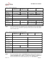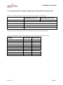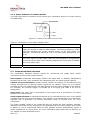
1
MV-D640 User’s Manual
All information provided in this manual is believed to be accurate and reliable. No
responsibility is assumed by Photonfocus AG for its use. Photonfocus AG reserves the right
to make changes to this information without notice.
Reproduction of this manual in whole or in part, by any means, is prohibited without prior
permission having been obtained from Photonfocus AG.
REV: 2.0
Page 2
MV-D640 User’s Manual
Contents
1 Preface ..............................................................................................................5
1.1
About Photonfocus .......................................................................................5
1.2
Contact ......................................................................................................5
1.3
Sales Offices ...............................................................................................5
1.4
Further information......................................................................................5
2 How to Get Started..............................................................................................6
2.1
First Steps with a MV-D640 CameraLink Model.................................................6
2.2
First Steps with a MV-D640 USB2.0 Model.......................................................7
3 Product Specification............................................................................................9
3.1
Introduction................................................................................................9
3.2
Technical Specification .................................................................................9
3.3
Frame grabber relevant Configuration (CameraLink models only) ..................... 12
4 Functionality..................................................................................................... 13
4.1
Image Acquisition ...................................................................................... 13
4.2
4.1.1
Free-running and Trigger Mode ........................................................ 13
4.1.2
Exposure Control ........................................................................... 13
4.1.3
Maximum Frame Rate..................................................................... 13
4.1.4
Sensor Read-out Mode.................................................................... 13
Pixel Response .......................................................................................... 14
4.3
4.2.1
Linear Response ............................................................................ 14
4.2.2
Analog Gain .................................................................................. 14
4.2.3
Digital Gain ................................................................................... 14
Bayer Color Pattern.................................................................................... 15
4.4
Test Image ............................................................................................... 15
4.5
Reduction of Image Size ............................................................................. 16
4.6
4.5.1
Region of Interest .......................................................................... 16
4.5.2
ROI Example Configurations ............................................................ 16
4.5.3
Frame Rate Calculation Formula ....................................................... 17
External Trigger and Strobe ........................................................................ 18
4.7
4.6.1
Trigger Source............................................................................... 18
4.6.2
Trigger Mode ................................................................................. 18
4.6.3
Strobe Output ............................................................................... 20
Black Level Adjustment .............................................................................. 20
4.8
Configuration Interface............................................................................... 20
4.8.1
4.8.2
CameraLink Interface ..................................................................... 20
USB 2.0 Interface .......................................................................... 21
5 Hardware Interface............................................................................................ 23
5.1
Connectors ............................................................................................... 23
5.2
5.1.1
CameraLink Connector.................................................................... 23
5.1.2
USB2.0 Connector.......................................................................... 23
5.1.3
Power Supply ................................................................................ 23
5.1.4
Trigger and Strobe Signals for USB2.0 models ................................... 23
5.1.5
Status Indicator for CameraLink Models ............................................ 24
5.1.6
Status Indicator for USB2.0 Models .................................................. 25
CameraLink Data Interface ......................................................................... 25
5.3
Read-out Timing........................................................................................ 26
REV: 2.0
Page 3
MV-D640 User’s Manual
5.3.1
5.3.2
5.3.3
Free Running Mode ........................................................................ 26
External Trigger Mode..................................................................... 28
Trigger Delay ................................................................................ 29
6 Mechanical and Optical Considerations.................................................................. 30
6.1
Mechanical Interface .................................................................................. 30
6.2
Optical Interface........................................................................................ 32
6.2.1
6.2.2
Mounting the Lens.......................................................................... 32
Cleaning the Sensor ....................................................................... 32
7 Warranty.......................................................................................................... 34
7.1
Warranty Terms ........................................................................................ 34
7.2
Warranty Claim ......................................................................................... 34
8 Pinouts ............................................................................................................ 35
8.1
Power Supply ............................................................................................ 35
8.2
8.1.1
Power Supply Connector for CameraLink Model .................................. 35
8.1.2
Power Supply Connector for USB2.0 Model ........................................ 36
CameraLink Connector ............................................................................... 36
8.3
USB2.0 Connector ..................................................................................... 37
9 Troubleshooting ................................................................................................ 38
9.1
Common pitfalls with microDisplay USB and PFRemote ................................... 38
10 References ....................................................................................................... 39
11 Appendix A – Pseudo random number generator .................................................... 40
12 Appendix B – Adjusting the Black Level Offset with PFRemote 0.65........................... 43
13 Appendix C – CE Compliance Statement ............................................................... 44
14 Appendix D - Revision History ............................................................................. 45
REV: 2.0
Page 4
MV-D640 User’s Manual
1
Preface
1.1 About Photonfocus
The Swiss company Photonfocus is one of the leading specialists in the development of
CMOS image sensors and corresponding industrial cameras for machine vision, security &
surveillance and automotive markets.
Photonfocus is dedicated to making the latest generation of CMOS technology commercially
available. Active Pixel Sensor (APS) and global shutter technologies enable high speed and
high dynamic range (120 dB) applications, while avoiding disadvantages, like image lag,
blooming and smear.
Photonfocus has proven that the image quality of modern CMOS sensors is now
appropriate for demanding applications. Photonfocus' product range is complemented by
custom design solutions in the area of camera electronics and CMOS image sensors.
Photonfocus is ISO 9001 certified. All products are produced with the latest techniques in
order to ensure the highest degree of quality.
1.2 Contact
Photonfocus AG, Bahnhofplatz 10, CH-8853 Lachen SZ, Switzerland
Sales
Support
Phone: +41 55 451 01 31
Phone: +41 55 451 01 37
Email: [email protected]
Email: [email protected]
1.3 Sales Offices
Photonfocus products are available through an extensive international distribution network;
details of the distributor nearest to you can be found at www.photonfocus.com.
1.4 Further information
For further information on the products, documentation and software updates please see
our website www.photonfocus.com or contact our distributors.
Photonfocus reserves the right to make changes to its products and documentation without
notice. Photonfocus products are neither intended nor certified for use in life support
systems or in other critical systems. The use of Photonfocus products in such applications
is prohibited.
Photonfocus and LinLog™ are trademarks of Photonfocus AG. CameraLink is a registered
mark of the Automated Imaging Association. Product and company names mentioned
herein are trademarks or trade names of their respective companies.
Reproduction of this manual in whole or in part, by any means, is prohibited without prior
permission having been obtained from Photonfocus AG.
Photonfocus cannot be held responsible for any technical or typographical errors.
REV: 2.0
Page 5
MV-D640 User’s Manual
2
How to Get Started
2.1 First Steps with a MV-D640 CameraLink Model
1.
Remove the camera from its package.
Please make sure the following items are included with your camera:
•
3-pole power supply plug
•
Camera body cap
If any items are missing or damaged, please contact your dealership.
2.
Install the frame grabber software.
Note:
3.
4.
Without installed frame grabber software the camera configuration tool
PFRemote will not be able to communicate with the camera. Please follow
the instructions of the frame grabber supplier.
Remove the protective cap from the camera and mount a suitable lens.
Caution:
Protect the image sensor from particles and dust! Remove the
protective cap from the C-mount thread of the sensor module and screw
in the lens. When removing the protective cap or changing the lens, the
camera should always be held with the opening facing downwards to
prevent dust falling onto the CMOS sensor.
Note:
For US and Canada: Ensure a UL listed power supply is used.
Download the PFInstaller from the Photonfocus website and install the software.
Run PFInstaller.exe. Follow the instructions of the installer and choose "Any CameraLink compliant grabber". Then follow the instructions described in the readme file.
5.
Connect the delivered power supply to the camera.
Caution:
Check the correct power supply voltage and polarity! Do not exceed the
maximum operating voltage of +5V DC (+10%, -5%) for the CameraLink
model.
6.
Connect the camera to your frame grabber with a CameraLink cable.
7.
Start the camera software PFRemote.
Double click on the communication port where you attached the camera.
8.
Check the status LEDs on the rear side of the camera.
See Section 5.1.6 for more information.
9.
You may now display images using the software provided by your frame grabber
manufacturer.
REV: 2.0
Page 6
MV-D640 User’s Manual
2.2 First Steps with a MV-D640 USB2.0 Model
10. Remove the camera from its package.
Please make sure the following items are included with your camera:
•
7-pole power supply plug
•
Camera body cap
If any items are missing or damaged, please contact your dealership.
11. Check if your computer fulfils the hardware requirements.
See Section 4.8.2 for more information.
12. Remove the protective cap from the camera and mount a suitable lens.
Caution:
Protect the image sensor from particles and dust! Remove the
protective cap from the C-mount thread of the sensor module and screw
in the lens. When removing the protective cap or changing the lens, the
camera should always be held with the opening facing downwards to
prevent dust falling onto the CMOS sensor.
Note:
For US and Canada: Ensure a UL listed power supply is used.
13. Download the PFInstaller from the Photonfocus website and install the software.
Run PFInstaller.exe. Follow the instructions of the installer and choose "Any
Photonfocus USB camera".
Important: During the installation, the camera must not be connected to the USB
port.
14. Connect the delivered power supply to the camera.
Caution:
Check the correct power supply voltage and polarity! Do not exceed the
maximum operating voltage of +12V DC (± 10%) for the USB2.0 model.
15. Connect the camera to your computer with a USB2.0 cable.
16. Let Windows install the driver.
Windows should display the "New Hardware found" wizard automatically. If this wizard
is not displayed, please continue as described under "Manual Driver Installation"
below.
Let the Hardware assistant install the drivers. It is not necessary to allow the search
for current and updated software on the Internet. Proceed by choosing the option
"Install the software automatically (Recommended)". Another Hardware Installation
message will appear which can be ignored ("Continue Anyway").
Note:
The procedure described here applies to Windows XP SP2.
17. Start the software microDisplay USB.
If you are not familiar with the microDisplay USB software please read the manual
[MAN025] before acquiring images.
Important: Always start the software microDisplay USB in the first step and proceed
to start the camera software PFRemote in the second step. This is
mandatory for proper operation of the camera, because microDisplay USB
downloads the USB firmware into the camera.
REV: 2.0
Page 7
MV-D640 User’s Manual
Each time the power supply or the USB cable have been disconnected, you
have to restart microDisplay USB in order to download the firmware again.
18. Start the camera software PFRemote.
Double click on the communication port "USB0".
19. Check the status LEDs.
See Section 5.1.6 for more information.
20. You may now display images using microDisplay USB.
Note:
The maximum frame rate depends on the USB chipset of the PC and on the
camera parameters.
Manual driver installation
If Windows did not automatically install the driver for your USB camera, please proceed
as follows:
•
Open the Device Manager in the Windows Control Panel.
•
There will be an unknown device called "Silicon Software microUSB2".
•
Right click on the unknown device and choose "Update Driver".
•
The Hardware update wizard will appear. It is not necessary to allow the search for
current and updated software on the Internet. Click on "No, not this time" and
"Next".
•
Then choose "Install the software automatically (Recommended)" and proceed with
"Next".
•
When you get asked for the driver location, specify
\Photonfocus\microDisplayUSB\driver.
Note:
REV: 2.0
This procedure applies to Windows XP SP2.
Page 8
MV-D640 User’s Manual
3
Product Specification
3.1 Introduction
The MV-D640 camera series from Photonfocus is aimed at demanding applications in
industrial image processing. The cameras offer a high dynamic range of up to 60 dB with a
resolution of 640x480 pixels and a full frame rate of up to 200 frames per second. The
principal advantages are:
•
Superior color rendition
•
Exceptional linear response curve
•
Superior SNR (signal to noise ratio)
•
Low power consumption at high speeds
•
Resistance to blooming
•
Ideal for high speed applications: Global shutter, in combination with a selectable
region of interest to increase speed
•
USB2.0 or CameraLink interface
•
Compact size
3.2 Technical Specification
Table 1: Sensor parameters
MV-D640 Series
Technology
Scanning system
Shutter type
CMOS active pixel
progressive scan
global shutter
Resolution
640 x 480 pixels
Optical format / diagonal
1/2" / 7.92 mm
Pixel size
9.9 μm x 9.9 μm
Active optical area
Random Noise
Fixed Pattern Noise
Full well capacity
Spectral range
Responsivity
6.34 mm x 4.75 mm
< 0.59 DN RMS @ 630 nm / 8 bit / gain = 1
< 1.5 DN RMS @ 630 nm / 8 bit / gain = 1
90 ke400 nm … 1000 nm
480 x 103 DN / (J/m2)
@ 630 nm / 8 bit / gain = 1
Optical fill factor
50 %
Dynamic range
60 dB
Color format
monochrome / color (Bayer pattern)
Characteristic curve
linear
Shutter mode
global
Read-out mode
REV: 2.0
sequential or interleaved (automatically determined)
Page 9
MV-D640 User’s Manual
Table 2: Camera parameters
MV-D640-66-CL-10
MV-D640-33-CL-10
MV-D640C-66-CL-10 MV-D640C-33-CL-10
Frame rate
MV-D640C-48-U2-8
50 μs – 1.3 s
Exposure time
Exposure time
step size
MV-D640-48-U2-8
20 μs
20 μs
16 μs
48 μs
up to 200 fps
up to 100 fps
up to 129 fps
up to 42 fps
Min. region of
interest (ROI)
4x1 pixels
Width x height ≥ 1024 pixels
Grayscale
resolution
8 / 10 bit
8 bit
Digital gain
x1, x2, x4
Analog gain
x1 … x8 (up to x18 possible, but not recommended)
Pixel clock
frequency
Pixel clock period
66 MHz
33 MHz
48 MHz (fast USB)
24 MHz (slow USB)
16 MHz (fast USB)
8 MHz (slow USB)
15.15 ns
30.30 ns
20.83 ns (fast (USB)
62.5 ns (fast USB)
41.67 ns (slow USB)
125 ns (slow USB)
Camera taps
Note:
1
The maximum frame rate depends on the configuration and the USB chipset
on the PC. For more information regarding the fast and slow USB mode please
refer to Section 4.8.2.
Table 3: Physical characteristics and operating ranges
MV-D640-66-CL-10
MV-D640-33-CL-10
MV-D640C-66-CL-10 MV-D640C-33-CL-10
Operating
temperature
MV-D640-48-U2-8 MV-D640C-48-U2-8
0 °C … 60 ºC
Camera power
supply
+5V DC (+10%, -5%)
+12V DC (± 10%)
Trigger signal
input range
–
+5 … +15V DC
Strobe signal
power supply
–
+5 … +15V DC
Strobe signal sink
current (average)
–
max. 8mA
Power
consumption
1.7 W
1.5 W
Lens mount
Dimensions
Mass
Conformity
Note:
REV: 2.0
3.3 W
C-mount
55 x 55 x 37 mm3
55 x 55 x 48 mm3
200 g
200 g
CE / UL
For US and Canada: Ensure an UL listed power supply marked "Class 2" is
used and rated 5V DC/min. 400mA or 12V DC/min. 400mA, respectively. A
suitable UL listed power supply is available from Photonfocus. Ensure the
device downstream of the camera data path (eg: PC) is UL listed also.
Page 10
MV-D640 User’s Manual
Monochrome
Color
Figure 1: Quantum efficiency as function of wavelength
REV: 2.0
Page 11
MV-D640 User’s Manual
3.3 Frame grabber relevant Configuration (CameraLink models only)
Table 4: Summary of parameters needed for frame grabber configuration
MV-D640(C)-66-CL-10
Pixel clock per tap
MV-D640(C)-33-CL-10
66 MHz
33 MHz
CC1
EXSYNC
CC2
–
CC3
–
CC4
–
Camera port and bit assignments are compliant to the CameraLink standard.
Table 5: CameraLink port and bit assignment for MV-D640 CameraLink series
Data Bit
Tap 0, 8 bit
Tap 0, 10 bit
0 (LSB)
A0
A0
1
A1
A1
2
A2
A2
3
A3
A3
4
A4
A4
5
A5
A5
6
A6
A6
7 (MSB for 8 bit mode)
A7
A7
8
B0
9 (MSB for 10 bit mode)
B1
REV: 2.0
Page 12
MV-D640 User’s Manual
4
Functionality
This chapter serves as an overview of the camera configuration modes and explains
camera features.
4.1 Image Acquisition
4.1.1 Free-running and Trigger Mode
By default the camera continuously delivers images as fast as possible ("Free-running
mode").
When the acquisition of an image needs to be synchronised to an external event, an
external trigger can be used (refer to Sections 4.6 and 5.1.4). In this mode, the camera is
idle until it receives a signal to capture an image.
4.1.2 Exposure Control
The exposure time defines the period during which the image sensor integrates the
incoming light. Refer to Table 2 for the allowed exposure time range and see Section 5.2.
4.1.3 Maximum Frame Rate
The maximum frame rate depends on the exposure time and the size of the image (Region
of Interest ROI, see Section 4.5). Depending on the exposure time and ROI size, the
sensor is configured automatically in interleaved or non-interleaved mode (see Sections
4.1.4 and 4.5).
4.1.4 Sensor Read-out Mode
For an exposure time smaller than the read-out time, the sensor is operated in noninterleaved mode. To further increase the frame rate, the sensor is operated in interleaved
mode when the exposure time is longer than the read-out time.
Note:
The camera chooses the most advantageous mode (interleaved / noninterleaved) automatically without user-intervention.
Interleaved mode integrates an image while reading out the last image (see Figure 2) and
does therefore increase the maximum frame rate.
Important: In external trigger mode, the camera will always be configured automatically
in non-interleaved mode.
REV: 2.0
Page 13
MV-D640 User’s Manual
Figure 2: Difference between interleaved and non-interleaved mode
Following table gives the exposure time at which the read-out mode is switched for the full
resolution of 640x480 pixels. See Section 4.5.3 for the calculation of the frame rate.
Table 6: Switching of the read-out mode for a full frame of 640x480
Exposure time
Interleaved mode
Non-interleaved mode
MV-D640(C)-66-CL-10
< 4.9 ms
≥ 4.91 ms
MV-D640(C)-33-CL-10
< 9.8 ms
≥ 9.8 ms
MV-D640-48-U2-8
< 7.8 ms (fast USB mode)
≥ 7.8 ms (fast USB mode)
< 15.6 ms (slow USB mode)
≥ 15.6 ms (slow USB mode)
< 23.1 ms (fast USB mode)
≥ 23.1 ms (fast USB mode)
< 46.2 ms (slow USB mode)
≥ 46.2 ms (slow USB mode)
MV-D640C-48-U2-8
4.2 Pixel Response
4.2.1 Linear Response
Normally, the camera offers a linear response between input light signal and output gray
level. In addition, a linear analog or digital gain may be applied.
4.2.2 Analog Gain
The MV-D640 camera series offer an analog on-chip gain between x1 and x18 in steps of 1.
For the color model, the four color channels red, green1, blue, green2 can be adjusted
independently.
Important! Using a high analog gain will degrade the image quality. Although it is
possible to configure analog gain up to x18, we strongly recommend using a
lower gain than gain x8.
REV: 2.0
Page 14
MV-D640 User’s Manual
4.2.3 Digital Gain
Gain x2 and x4 is a digital amplification, which means that the digital image data are
multiplied by a factor 2 or 4 respectively, in the camera.
4.3 Bayer Color Pattern
The MV-D640 color model is equipped with a Bayer color pattern. A full RGB signal can be
calculated using a Bayer algorithm. For the CameraLink models, this is performed by the
frame grabber. For the USB2.0 model, the Bayer algorithm is performed in the camera.
(0,0) = Bottom left corner of sensor arrray
Figure 3: Bayer pattern example
Note:
When using a region of interest, the start point for the Bayer decoder depends
on the start point of the ROI.
Note:
For the MV-D640C-66-CL model, the start point of the Bayer decoder must be
reconfigured when switching between the fast (66 MHz) and slow (33 MHz)
mode:
33 MHz mode: Pixel (0,0) = green
66 MHz mode: Pixel (0,0) = red
Important!
All Photonfocus
equipment. It is
replaced by one
image in difficult
color cameras are fitted with an IR/UV blocking filter as standard
possible that, depending on the illumination source, this filter must be
corresponding to the illumination source, in order to achieve an optimal
illumination environments (e.g. halogen lamp with high red component).
4.4 Test Image
An LFSR (Linear Feedback Shift Register) test image outputs a constant pattern with a
pseudo-random gray level sequence containing every possible gray level that is repeated
for every row (Figure 23). Please refer to Chapter 11 for a detailed description of the LFSR
pattern.
REV: 2.0
Page 15
MV-D640 User’s Manual
4.5 Reduction of Image Size
4.5.1 Region of Interest
Some applications do not need full image resolution. By reducing the image size to a
certain region of interest (ROI), the frame rate can be drastically increased. A region of
interest can be almost any rectangular window and is specified by its position within the
full frame and its width and height. Figure 4 gives some possible configurations for a region
of interest, and Table 7 shows some numerical examples of how the frame rate can be
increased by reducing the ROI.
Figure 4: ROI configuration examples
Note:
Only the reduction in y-direction (image height) results in a higher frame rate.
4.5.2 ROI Example Configurations
The following tables show how the frame rate is increased by reducing the number of rows.
The tables give round numbers, the actual maximum values could be slightly higher.
Table 7: Maximum image rates for the CameraLink models
ROI
texp = 50 µs
MV-D640-66-CL-10
MV-D640C-66-CL-10
MV-D640-33-CL-10
MV-D640C-33-CL-10
640 x 480
200 fps
100 fps
640 x 240
390 fps
200 fps
640 x 120
770 fps
390 fps
640 x 60
1490 fps
760 fps
640 x 30
2660 fps
1420 fps
REV: 2.0
Page 16
MV-D640 User’s Manual
Table 8: Maximum image rates for the USB2.0 camera models
ROI
MV-D640-48-U2-8
MV-D640C-48-U2-8
texp = 50 µs
Intel supported
chipset
(fast mode)
No Intel
supported chipset
(slow mode)
Intel supported
chipset
(fast mode)
No Intel
supported chipset
(slow mode)
640 x 480
129 fps
64 fps
43 fps
20 fps
640 x 240
255 fps
128 fps
85 fps
40 fps
640 x 120
500 fps
250 fps
165 fps
85 fps
640 x 60
960 fps
490 fps
330 fps
165 fps
640 x 30
1780 fps
930 fps
630 fps
320 fps
4.5.3 Frame Rate Calculation Formula
The frame rate depends on the exposure time and the ROI. For the USB models, the
maximum frame rate also depends on the USB chipset of the PC. Please refer to Section
4.8.2 for more information.
The frame rate can be calculated using the following formula:
treadout = tu * [CPRE + (Py + 2) * (Rx + HB) + RESET] * MODE
if texp < treadout,
tframe = texp + treadout
else
tframe = texp + tu * (CPRE + RESET) * MODE
end
Frame rate = 1/ tframe
Table 9: Symbols used in the frame rate calculation formula
CameraLink
USB2.0
MV-D640-66-CL
MV-D640-33-CL
MV-D640C-66-CL MV-D640C-33-CL
Horizontal
Blanking HB
3
127 + HB
RESET
Pixel clock
period tu
MODE
MV-D640C-48-U2
(color)
96
CPRE
Pixel clock fu
MV-D640-48-U2
(monochrome)
550
66 MHz
33 MHz
48 MHz
16 MHz
15.15 ns
30.30 ns
20.83 ns
62.5 ns
Constant MODE = 1
Intel supported chipset: MODE = 1
No Intel supported chipset: MODE = 2
Rx
Constant Rx = 671, independent of ROI
Py
Height of the ROI
texp
Exposure time in [s]
treadout
REV: 2.0
Read-out time [s]
Page 17
MV-D640 User’s Manual
Example 1: MV-D640-66-CL, ROI 100x100 pixel, exposure time texp = 6 ms
•
treadout = tu * [CPRE + (Py + 2) * (Rx + HB) + RESET] * MODE = 1.05 ms
•
treadout < texp Ö tframe = texp + tu * (CPRE + RESET) * MODE = 6.01 ms
•
Frame rate = 1 / tframe = 166 fps
Example 2: MV-D640C-33-CL, ROI 640x300 pixel, exposure time texp = 1 ms
•
treadout = tu * [CPRE + (Py + 2) * (Rx + HB) + RESET] * MODE = 6.19 ms
•
treadout > texp Ö tframe = texp + treadout = 7.19 ms
•
Frame rate = 1 / tframe = 139 fps
Example 3: MV-D640C-48-U2, ROI 200x100 pixel, exposure time texp = 5 ms, Intel
supported chipset (fast mode)
•
treadout = tu * [CPRE + (Py + 2) * (Rx + HB) + RESET] * MODE = 4.94 ms
treadout < texp Ö tframe = texp + tu * (CPRE + RESET) * MODE = 5.05 ms
•
Frame rate = 1 / tframe = 198 fps
•
Example 4: MV-D640C-48-U2, ROI 200x100 pixel, exposure time texp = 5 ms,
no Intel supported chipset (slow mode)
•
treadout = tu * [CPRE + (Py + 2) * (Rx + HB) + RESET] * MODE = 9.88 ms
treadout > texp Ö tframe = texp + treadout = 14.88 ms
•
Frame rate = 1 / tframe = 67 fps
•
Note:
For a small ROI and small exposure time, the actual frame rate may differ
from this calculated value due to the minimum exposure step size as defined
in Table 2.
4.6 External Trigger and Strobe
An external trigger is an event that starts an exposure. If a trigger signal is applied to the
camera during the exposure or read-out time, the trigger will be ignored.
4.6.1 Trigger Source
The MV-D640 camera models with CameraLink interface are triggered over the CC1 signal
via frame grabber.
The MV-D640 camera models with USB2.0 interface are triggered over a signal available on
the power supply connector (see Section 5.1.4).
Note:
For the USB models, both trigger and strobe must be configured in
microDisplay. See [MAN025] for more information.
4.6.2 Trigger Mode
In external trigger mode, the sensor is always operated in non-interleaved mode (compare
to Section 4.5). Figure 5 and Figure 6 compare the maximum frame rate in free running
and external trigger mode with increasing exposure time. In the free running mode, the
step in the curve indicates the switching between non-interleaved and interleaved mode.
REV: 2.0
Page 18
MV-D640 User’s Manual
CameraLink Models: MV-D640(C)-33-CL
200
free running, -66 model
180
external trigger, -66 model
Max. Frame Rate [fps]
160
free running, -33 model
140
external trigger, -33 model
120
100
80
60
40
20
0
0.0
10.0
20.0
30.0
40.0
50.0
60.0
Exposure tim e [m s]
Figure 5: Frame rate of MV-D640-66 camera in free running and external trigger mode
USB Models: MV-D640C-48-U2, MV-D640-48-U2
140
free running, mono model
Max. Frame Rate [fps]
120
external trigger, mono model
free running, color model
100
external trigger, color model
80
60
40
20
0
0.0
10.0
20.0
30.0
40.0
50.0
60.0
Exposure time [ms]
Figure 6: Frame rate of the USB2.0 models in free running and external trigger mode
REV: 2.0
Page 19
MV-D640 User’s Manual
4.6.3 Strobe Output
When using a CameraLink model, the strobe output must be provided by the frame
grabber.
For the USB models, there is an opto isolated strobe output on the power supply connector
available.
Note:
The strobe output needs a separate power supply due to the opto-coupled
output. Please see Section 5.1.4 for more information. For the configuration,
see [MAN025].
4.7 Black Level Adjustment
The black level offset (the mean value of the image when the lens aperture is completely
closed) is calibrated by factory for Gain=2 (default setting). Changing the gain may need
to adjust the black level offset with the following procedure:
1. Close the aperture of the lens, or close the lens opening of the camera with the
camera body cap.
2. In your frame grabber software, display a histogram of the captured black image. If
there is no histogram available, store the image and use a standard image
manipulation tool.
3. Open the camera in PFRemote 1.0.
4. In the 'Special' tab of PFRemote, change the value of 'Black Level Offset', until the
histogram of the black image looks as in Figure 7.
5. To save the current settings including the new black level offset in the camera, use
the "Store as defaults" button.
Figure 7: Histogram for a correct black level
Note:
For PFRemote version 0.65, refer to Chapter 12.
4.8 Configuration Interface
4.8.1 CameraLink Interface
A CameraLink camera can be controlled by the user via an RS232 compatible asynchronous
serial interface. This interface is contained within the CameraLink interface as shown in
Figure 8 and is physically not directly accessible. Instead, the serial communication is
usually routed through the frame grabber. For some frame grabbers it might be necessary
to connect a serial cable from the frame grabber to the serial interface of the PC.
REV: 2.0
Page 20
MV-D640 User’s Manual
Figure 8: CameraLink serial interface for camera communication
To interface different cameras to different frame grabbers, the CameraLink standard
defines a software API. It defines how the functions to initialise, read from, write to and
close the serial interface should look. The code behind these functions is frame grabber
specific and is written by the frame grabber manufacturer. The functions are then compiled
into a DLL called clserXXX.dll, where XXX is a unique identifier for the frame grabber
manufacturer.
The PFRemote camera configuration tool as well as the PFLib API use the serial interface to
communicate with the camera and to control its functions. The serial interface is accessed
via the clserXXX.dll. Therefore, the appropriate clserXXX.dll for the frame grabber
manufacturer needs to be in the same directory as the PFRemote executable (e.g.
C:\Program Files\Photonfocus\PFRemote). This DLL is usually located in the windows\system32
directory after installing the frame grabber driver.
The serial configuration parameters are defined in the CameraLink standard and are as
follows: 9600 baud, 1 start bit, 1 stop bit, no parity, no handshaking.
4.8.2 USB 2.0 Interface
The abbreviation USB stands for “Universal Serial Bus” and is a bus system developed in
1995 by a consortium of leading companies in the computer industry, in cooperation with
Intel. The USB 1.1 specification defined a port speed to be 12 MBit/s, the USB 2.0
specification a remarkable 480 MBit/s. However, not every PC with an USB 2.0 interface
can be used in the fast mode to reach a maximum speed of data transfer (24 MByte/s or
48 MByte/s). Depending on the available USB chipset on the PC, it is possible that only a
data rate of 24 MByte/s can be achieved.
Note:
The maximum speed of the USB interface (24 MByte/s or 48 MByte/s) is
determined by the USB driver automatically and cannot be configured.
Software requirements
To reach the full performance of 48 MByte/s, Windows XP with Service Pack 2 is required.
For Windows 2000 and Windows XP with Service Pack 1, the camera will run with 24
Mbyte/s only.
Note:
REV: 2.0
The camera can only be operated with the software MicroDisplay USB to grab
images, together with PFRemote to control the camera. Alternatively, the
frame grabber module USB SDK and the PFLib SDK can be used. Other
software is not supported.
Page 21
MV-D640 User’s Manual
Attention: The camera firmware, which is essential for the operation of the camera, is
automatically transmitted to the camera via USB during the start-up of the
MicroDisplay USB software. Therefore, the camera must always be connected
to the USB port during start up, otherwise the camera will not be functional.
Hardware requirements
To reach the full performance of 48 Mbyte/s (isochronous mode), a PC Mainboard with
Intel chipsets is required and the Southbridge must support ICH4, ICH5 or higher. The
camera must be connected to a USB port that is provided by the Southbridge of the PC and
not by an additional USB2.0 host adapter. More information about the Southbridge is
available in the motherboard manual of your PC. A list of Intel chip sets is available at
www.intel.com/products/chipsets/index.htm.
Note:
Intel provides the tool chiputil.exe to determine the chip set being used on a PC.
It can be downloaded from:
ftp://aiedownload.intel.com/df-support/7355/eng/chiputil.exe
Alternative link: http://downloadfinder.intel.com/scripts-df/support_intel.asp (search
for ’chiputil’)
Note:
The camera is optimised for high data transfer, and other USB devices may
stop functioning or perform poorly.
Note:
Additional USB 2.0 host adapters may only transfer up to 24 Mbyte/s because
they are not directly connected to the Southbridge and therefore do not
support the isochronous mode.
The data transfer mode of the camera (48 MByte/s or 24 MByte/s) is indicated by the
upper LED on the back of the camera (see Section 5.1.5) or in the Info tab of PFRemote.
REV: 2.0
Page 22
MV-D640 User’s Manual
5
Hardware Interface
5.1 Connectors
5.1.1 CameraLink Connector
The CameraLink cameras are interfaced to external components via a CameraLink
connector, which is defined by the CameraLink standard as a 26 pin, 0.5" Mini D-Ribbon
(MDR) connector to transmit configuration, image data and trigger.
The CameraLink interface and connector are specified in [CL]. For further details including
the pinout please refer to Chapter 8. This connector is used to transmit configuration,
image data and trigger signals.
5.1.2 USB2.0 Connector
The USB 2.0 camera model is interfaced to external components via USB 2.0 (B-Type)
connector (see Figure 9).
Figure 9: USB 2.0 Type B connector
5.1.3 Power Supply
The camera requires a single voltage input (see Table 3). The camera meets all
performance specifications using standard switching power supplies, although wellregulated linear power supplies provide optimum performance.
Warning:
It is extremely important that you apply the appropriate voltage to your
camera. Incorrect voltage will damage the camera.
Important: For US and Canada: Ensure a UL listed power supply is used. A suitable UL
listed power supply is available from Photonfocus.
For further details including the pinout please refer to Section 8.
5.1.4 Trigger and Strobe Signals for USB2.0 models
The power connector contains an external trigger input and a strobe output.
Warning:
REV: 2.0
The input voltage to the TRIGGER pin must not exceed +15V DC, to avoid
damage of the optocoupler!
Page 23
MV-D640 User’s Manual
In order to use the strobe, the optocoupler must be powered with 5 .. 15 V DC. The
STROBE signal is an open-collector output, therefore, the user must connect a pull-up
resistor (see Table 10) to STROBE_VDD (5 .. 15 V DC) as shown in Figure 10. This resistor
should be located directly at the signal receiver.
Figure 10: Circuit for the Trigger/Shutter signals (USB)
Caution:
The maximum sink current of the STROBE pin is 8 mA. Do not connect
inductive or capacitive loads, such loads may result in damage of the
optocoupler!
Table 10: Pull-up resistor for the strobe output
STROBE_VDD
Pull-up Resistor
15 V
> 3.9 kOhm
10 V
> 2.7 kOhm
8V
> 2.2 kOhm
7V
> 1.8 kOhm
5V
> 1.0 kOhm
5.1.5 Status Indicator for CameraLink Models
A dual-color LED on the back of the camera gives information about the current status.
LED Green
Green when an image is output. At slow frame rates, the LED blinks with
the FVAL signal. At high frame rates the LED changes to an apparently
continuous green light, with intensity proportional to the ratio of readout
time over frame time.
LED Red
Red indicates an active serial communication with the camera.
REV: 2.0
Page 24
MV-D640 User’s Manual
5.1.6 Status Indicator for USB2.0 Models
Two dual-color LEDs on the back of the camera give information about the current camera
and USB status.
Figure 11: Position of the status indicator LEDs
Table 11: Description of the status indicator LEDs
LED 1 Green
Green when a physical USB connection is established.
LED 1 Red
After the USB-firmware was uploaded to the camera by microDisplay
USB, the camera is ready for data transfer. The blinking frequency of the
red LED indicates the current transfer mode. In the slow mode (24
MByte/s), the blinking interval is 1 Hz, in the fast mode (48 Mbyte/s) it is
4 Hz.
LED 2 Green
Green when an image is output. At slow frame rates, the LED blinks with
the FVAL signal. At high frame rates the LED changes to an apparently
continuous green light, with intensity proportional to the ratio of readout
time over frame time.
LED 2 Red
Red indicates active serial communication with the camera.
5.2 CameraLink Data Interface
The CameraLink standard contains signals for transferring the image data, control
information and the serial communication.
Data signals: CameraLink data signals contain the image data. In addition, handshaking
signals such as FVAL, LVAL and DVAL are transmitted over the same physical channel.
Camera control information: Camera control signals (CC-signals) can be defined by the
camera manufacturer to provide certain signals to the camera. There are 4 CC-signals
available and all are unidirectional with data flowing from the frame grabber to the camera.
For example, the external trigger is provided by a CC-signal (see Table 4 for the CC
assignment).
Pixel clock: The pixel clock is generated on the camera and is provided to the frame
grabber for synchronisation.
Serial communication: A CameraLink camera can be controlled by the user via an RS232
compatible asynchronous serial interface. This interface is contained within the CameraLink
interface and is physically not directly accessible. Refer to Section 4.8.1 for more
information.
The frame grabber needs to be configured with the proper tap and resolution settings,
otherwise the image will be distorted or not displayed with the correct aspect ratio. Refer
to Section 3.3 for a summarised table of frame grabber relevant specifications. Figure 8
shows symbolically a 1-tap system. For more information about taps refer to [AN021] on
our website on www.photonfocus.com.
REV: 2.0
Page 25
MV-D640 User’s Manual
5.3 Read-out Timing
5.3.1 Free Running Mode
By default, the camera is in free running mode and delivers images without any external
control signals. Depending on the exposure and read-out time, the sensor is operated
either in interleaved or non-interleaved mode.
Non-Interleaved Mode
If the read-out time exceeds the exposure time, the sensor is automatically operated in
non-interleaved mode, which means that the sensor is read out after the preset exposure
time. Then the sensor is reset, a new exposure starts and the readout of the image
information begins again. The data is output on the rising edge of the pixel clock. The
signals FRAME_VALID (FVAL) and LINE_VALID (LVAL) mask valid image information. The
signal SHUTTER indicates the active integration phase of the sensor and is shown for clarity
only.
Figure 12 visualises the timing behaviour of the control and data signals in the noninterleaved mode.
Figure 12: Timing Diagram frame read-out in free-running, non-interleaved mode
REV: 2.0
Page 26
MV-D640 User’s Manual
Table 12: Explanation of control and data signals used in the timing diagram
Frame time
Maximum frame time is defined as exposure time plus data read
out time.
Exposure time
Period during which the pixels are integrating the incoming light.
PCLK
Pixel clock on CameraLink interface.
SHUTTER
Internal signal, shown only for clarity. Is ’high’ during the
exposure time, during which the pixels integrate the incoming
light and the image is acquired.
FVAL (Frame Valid)
Is ’high’ while the data of one whole frame are transferred.
LVAL (Line Valid)
Is ’high’ while the data of one line are transferred. Example: To
transfer an image with 640x480 pixels, there are 480 LVAL
within one FVAL active high period. One LVAL lasts 640 pixel
clock cycles.
DVAL (Data Valid)
Is ’high’ while data are valid.
DATA
Transferred pixel values. Example: For a 100x100 pixel image,
there are 100 values transferred within one LVAL active high
period, or 100*100 values within one FVAL period.
Line pause LP
Delay after the first line and after every following line except the
last when reading out the image data.
LP = Rx – Px + HB (Px = image width)*
LP_F
First line pause in an FVAL period.
LP_F = 2 * (Rx + HB) + 16*
LP_L
Last line pause in an FVAL period.
LP_L = 13 + HB*
CPRE
Constant delay between end of exposure time and beginning of
read-out.
RESET
Constant delay between end of read-out and earliest begin of a
new exposure.
*
Compare with Section 4.5.3.
Interleaved Mode
If the read-out time is smaller than the exposure time, the sensor is automatically
operated in interleaved mode, which means that during the exposure of the next image,
the last image is read out. Then the sensor is reset and a new exposure starts and the
readout of the image information begins again. The data is output on the rising edge of the
pixel clock. The signals FRAME_VALID (FVAL) and LINE_VALID (LVAL) mask valid image
information. The signal SHUTTER indicates the active integration phase of the sensor and is
shown for clarity only.
Figure 13 visualises the timing behaviour of the control and data signals in the interleaved
mode.
REV: 2.0
Page 27
MV-D640 User’s Manual
Figure 13: Timing Diagram frame read-out in free-running, interleaved mode
5.3.2 External Trigger Mode
In the external trigger mode, the exposure is defined by the camera and is configurable by
software. For an active high trigger signal, the image acquisition begins with the rising
edge of the trigger signal. The image is read out after the pre-configured exposure time.
After the readout, the sensor returns to the reset state and the camera waits for a new
trigger pulse (see Figure 14).
Note:
In external trigger mode, the camera is always operated in non-interleaved
mode.
The data is output on the rising edge of the pixel clock, the handshaking signals
FRAME_VALID (FVAL) and LINE_VALID (LVAL) mask valid image information. The signal
SHUTTER in Figure 14 indicates the active integration phase of the sensor and is shown for
clarity only.
REV: 2.0
Page 28
MV-D640 User’s Manual
Figure 14: Timing diagram for external trigger
5.3.3 Trigger Delay
MV-D640 CameraLink Models
The total delay between the trigger edge and the camera exposure consists of the delay in
the frame grabber and the camera.
For the delay in the frame grabber, please ask your frame grabber manufacturer. The
camera delay consists of a constant trigger delay and a variable delay (jitter).
Table 13: Maximum camera trigger delay (CameraLink models)
Camera Model
Trigger Delay td (constant)
Max. Trigger Jitter ti
MV-D640(C)-66-CL
15 ns
15 ns
MV-D640(C)-33-CL
30 ns
30 ns
MV-D640 USB2.0 Models
The delay between a trigger edge applied via the trigger pin on the power supply connector
consists of a constant and a variable delay as shown in Table 15.
Table 14: Maximum camera trigger delay (USB2.0 models)
Camera Model
Trigger Delay td (constant)
Max. Trigger Jitter tj
MV-D640-48-U2
500 ns
250 ns
MV-D640C-48-U2
500 ns
250 ns
REV: 2.0
Page 29
MV-D640 User’s Manual
6
Mechanical and Optical Considerations
6.1 Transport
During storage and transport, the camera should be protected against vibration, shock,
moisture and dust. The original packaging protects the camera adequately from vibration
and shock during storage and transport. Please either retain this packaging for possible
later use or dispose of it to local regulations.
6.2 Mechanical Interface
The general mechanical data of the cameras are listed in Table 1 and Table 2.
REV: 2.0
Page 30
MV-D640 User’s Manual
Figure 15: CameraLinkTM back plate
Figure 16: USB 2.0 back plate
Figure 17: CameraLinkTM and USB front plate
REV: 2.0
Page 31
MV-D640 User’s Manual
6.3 Optical Interface
6.3.1 Mounting the Lens
Remove the protective cap from the C-/CS-mount thread of the camera and install the
lens. When removing the protective cap or changing the lens, the camera should always be
held with the opening facing downwards to prevent durst from falling into the CMOS
sensor. If the lens is removed, the protective cap should be refitted. If the camera is
opened in a dusty environment, we recommend the use of a constant stream of clean air in
front of the objective.
6.3.2 Cleaning the Sensor
The sensor is part of the optical path and should be handled like other optical components:
with extreme care.
Dust can obscure pixels, producing dark patches in the images captured. Dust is most
visible when the illumination is collimated. Dark patches in the images caused by dust or
dirt shift position as the angle of illumination changes. Dust is normally not visible when
the sensor is positioned at the exit port of an integrating sphere, where the illumination is
diffuse.
1. The camera should only be cleaned in ESD-safe areas by ESD-trained personnel
using wrist straps. Ideally, the sensor should be cleaned in a clean environment.
Otherwise, in dusty environments, the sensor will immediately become dirty again
after cleaning.
2. Use a high quality, low pressure air duster (e.g. Electrolube EAD400D compressed
air spray) to blow off loose particles. This step alone is usually sufficient to clean the
sensor of the most common contaminants.
Warning!
Workshop air supply is not appropriate and may cause permanent damage to the
sensor.
3. If further cleaning is requried, use a suitable lens wiper or Q-Tip moistened with an
appropriate cleaning fluid to wipe the sensor surface as described below. Cleaning
materials must be ESD-safe, lint-free and free from particles that may scratch the
sensor surface. For cleaning the sensor, Photonfocus recommends the products
available from the suppliers as listed in Table 15.
Warning!
Do not use ordinary cotton buds. These do not fulfil the above requirements and
permanent damage to the sensor may result.
4. Wipe the sensor carefully and slowly. First remove coarse particles and dirt from the
sensor using Q-Tips soaked in 2-propanol, applying as little pressure as possible.
Using a method similar to that used for cleaning optical surfaces, clean the sensor
by starting at any corner of the sensor and working towards the opposite corner.
Finally, repeat the procedure with methanol to remove streaks. It is imperative that
no pressure be applied to the surface of the sensor or to the black globe-top
material (if present) surrounding the optically active surface during the cleaning
process.
REV: 2.0
Page 32
MV-D640 User’s Manual
Table 15: Recommended materials for sensor cleaning
Product
Anticon Gold 9“ x 9“
Wiper
TX4025
Transplex
Small Q-Tips SWABS
BB-003
Large Q-Tips SWABS
CA-003
Point Slim HUBY-340
Methanol
Wiper
Swab
Q-Tips
2-Propanol (Iso-Propanol)
Fluid
REV: 2.0
Q-Tips
Q-Tips
Fluid
Supplier
Milliken
Texwipe
Texwipe
Hans J. Michael GmbH,
Germany
Hans J. Michael GmbH,
Germany
Sharp
Johnson Matthey GmbH,
Germany
Johnson Matthey GmbH,
Germany
Remark
ESD safe and suitable
for class 100
environments.
Semiconductor Grade
99.9 % min (Assay),
Merck 12,6024,
UN1230, slightly
flammable and
poisonous
Semiconductor Grade
99.5 % min (Assay),
Merck 12,5227,
UN1219, slightly
flammable
Page 33
MV-D640 User’s Manual
7
Warranty
The manufacturer alone reserves the right to recognize warranty claims.
7.1 Warranty Terms
The manufacturer warrants to distributor and end customer that for a period of two years
from the date of the shipment from manufacturer or distributor to end customer (the
“Warranty Period”) that:
•
•
the product will substantially conform to the specifications set forth in the applicable
documentation published by the manufacturer and accompanying said product, and
the product shall be free from defects in materials and workmanship under normal
use.
The distributor shall not make or pass on to any party any warranty or representation on
behalf of the manufacturer other than or inconsistent with the above limited warranty set.
7.2 Warranty Claim
The above warranty does not apply to any product that has been opened, modified or
altered by any party other than manufacturer, or for any defects caused by any use of the
product in a manner for which it was not designed, or by the negligence of any party other
than manufacturer.
REV: 2.0
Page 34
MV-D640 User’s Manual
8
Pinouts
8.1 Power Supply
The power supply plugs are available from Binder connectors at www.binder-connector.de.
Warning:
It is extremely important that you apply the appropriate voltages to your
camera. Incorrect voltages will damage or destroy the camera.
Important: For US and Canada: Ensure a UL listed power supply is used. A suitable UL
listed power supply is available from Photonfocus.
Figure 18: Power connector assembly
8.1.1 Power Supply Connector for CameraLink Model
Figure 19: Power supply plug for CameraLink model (rear view of plug, solder side)
Table 16: Pinout of the power supply connector (CameraLink model)
PIN
1
2
3
I/O
PW
PW
PW
REV: 2.0
Name
VDD
GND
VDD2
Description
+ 5 V voltage supply
Ground
Reserved
Page 35
MV-D640 User’s Manual
Table 17: Power supply connectors (Binder subminiatur series 712)
Connector Type
Order Nr.
3-pole, plastic
99-0405-00-03
3-pole, metal
99-0405-10-03
8.1.2 Power Supply Connector for USB2.0 Model
Figure 20: Power supply plug for USB2.0 model (rear view of plug, solder side)
Table 18: Pinout of the power supply connector (USB2.0 model)
PIN
1
2
3
4
5
6
7
I/O
PW
PW
PW
PW
O
I
PW
Name
VDD
GND
NC
Shutter-VDD
Shutter
Trigger
Ground
Description
+ 12 V DC (+/-10%) power supply
Ground
NC
+ 5 V DC (-/+ 10%)
Exposure Control (optically insulated)
External Trigger (optically insulated)
Signal Ground
Table 19: Power supply connectors (Binder subminiatur series 712)
Connector Type
Order Nr.
7-pole, plastic
99-0421-00-07
7-pole, metal
99-0421-10-07
8.2 CameraLink Connector
The pinout for the CameraLink 26 pin, 0.5" Mini D-Ribbon (MDR) connector is compliant to
the CameraLink standard ([CL]) and is listed here for reference only.
Figure 21: CameraLink connector 3M MDR-26 plug
REV: 2.0
Page 36
MV-D640 User’s Manual
Table 20: Pin assignments for the CameraLink MDR26 socket
PIN
1
2
3
4
5
6
7
8
9
10
11
12
13
14
15
16
17
18
19
20
21
22
23
24
25
26
S
I/O
PW
O
O
O
O
O
I
O
I
I
I
I
PW
PW
O
O
O
O
O
I
O
I
I
I
I
PW
PW
Name
SHIELD
N_XD0
N_XD1
N_XD2
N_XCLK
N_XD3
P_SERTOCAM
N_SERTOFG
N_CC1
P_CC2
N_CC3
P_CC4
SHIELD
SHIELD
P_XD0
P_XD1
P_XD2
P_XCLK
P_XD3
N_SERTOCAM
P_SERTOFG
P_CC1
N_CC2
P_CC3
N_CC4
SHIELD
SHIELD
Description
Shield
Negative LVDS Output, CameraLink DataD0
Negative LVDS Output, CameraLink DataD1
Negative LVDS Output, CameraLink DataD2
Negative LVDS Output, CameraLink Clock
Negative LVDS Output, CameraLink DataD3
Positive LVDS Input, Serial Communication to the camera
Negative LVDS Output, Serial Communication from the camera
Negative LVDS Input
Positive LVDS Input
Negative LVDS Input
Positive LVDS Input
Shield
Shield
Positive LVDS Output, CameraLink DataD0
Positive LVDS Output, CameraLink DataD1
Positive LVDS Output, CameraLink DataD2
Positive LVDS Output, CameraLink clock
Positive LVDS Output, CameraLink DataD3
Negative LVDS Input, Serial Communication to the camera
Positive LVDS Output, Serial Communication from the camera
Positive LVDS Input
Negative LVDS Input
Positive LVDS Input
Negative LVDS Input
Shield
Shield
8.3 USB2.0 Connector
The USB 2.0 interface and connector were developed by a group of companies (Intel,
Agere Systems, NEC, Hewlett-Packard, Philips, etc.) which are now organized in the USB
Implementers Forum (www.usb.org).
The USB connector is used to transmit configuration signals and image data. The pinout
complies with the standard USB pinout and is listed here for the sake of completeness.
Figure 22: USB Type B connector (front view)
Table 21: Pinout USB connector
Pin
1
2
3
4
IO
PWR
I/O
I/O
PWR
REV: 2.0
Name
VBUS
DATADATA+
GND
Description
+5V power supply
Negative Data
Positivie Data
Ground
Page 37
MV-D640 User’s Manual
9
Troubleshooting
9.1 Common pitfalls with microDisplay USB and PFRemote
Message "mEnable not found" appears after microDisplay USB was started
•
The USB driver is not installed correctly. Try reinstalling PFInstaller.
•
When the camera is connected to the USB bus and powered on, check if there is a
"Multifunction adapter" with the entry "Silicon Software GmbH microUSB2" in the
Windows device manager.
•
Reinstall the driver manually. It is located in \Photonfocus\microDisplayUSB\driver.
PFRemote cannot communicate
•
microDisplay USB must always be started before PFRemote, because it downloads
the USB firmware to the camera.
No image is output
•
Check if the camera is outputting images (check if the lower LED is green, see
Section 5.1.5 and 5.1.6). Maybe the camera is in external trigger mode and does
not receive a trigger signal.
•
The camera USB interface or power supply has been disconnected since the last
start of microDisplay USB. Restart microDisplay USB.
•
Due to the minimum data frame size that can be transferred by USB, the minimum
ROI must be at least 1024 bytes. Choose an ROI of Width x Height > 1024 pixels.
•
If there is already an earlier USB driver installed on your PC and you have problems
installing the new PFInstaller, please contact the Photonfocus support at
[email protected].
Camera clock on port A is inactive
•
A wrong hardware applet was downloaded to the camera when starting
microDisplay USB. Always choose the correct camera model at the start of
microDisplay USB.
•
The camera USB interface or power supply has been disconnected since the last
start of microDisplay USB. Restart microDisplay USB.
REV: 2.0
Page 38
MV-D640 User’s Manual
10 References
All referenced documents can be downloaded from our website at www.photonfocus.com.
CL
CameraLink Specification, January 2004
SW002
PFLib SDK Documentation, Photonfocus, August 2005
MAN025
microDisplay USB2.0 User Manual, Photonfocus, November 2005
AN007
Application Note “Camera Acquisition Modes”, Photonfocus, March 2004
AN010
Application Note “Camera Clock Concepts”, Photonfocus, July 2004
AN021
Application Note, “CameraLink”, Photonfocus, July 2004
AN026
Application Note, “LFSR Test Images”, Photonfocus, September 2005
REV: 2.0
Page 39
MV-D640 User’s Manual
11 Appendix A – Pseudo random number generator
In order to test the interface between camera and frame grabber, a 10-bit LFSR with
many-to-one feedback structure was implemented. An XOR feedback of taps 2 and 9 was
implemented for the maximum sequence length of 1023 states. The state 0 does not exist
in this implementation. The sequence starts with the value 1 at the beginning of each line.
The first 256 values are presented in Table 22. A resulting pattern of vertical stripes can be
seen in the acquired image (see Figure 23).
Table 22: States 0 – 127 of the pseudo random number generator
Nr. HEX BIN
Nr. HEX BIN
Nr. HEX BIN
Nr.
HEX BIN
0
32 331
64 0E0
96
0EC
001
1000000000
1000110011
0000011100
0011011100
1
002
0100000000
33 263
1100011001
65 1C0
0000001110
97
1D9
1001101110
2
004
0010000000
34 0C7
1110001100
66 380
0000000111
98
3B2
0100110111
3
009
1001000000
35 18F
1111000110
67 301
1000000011
99
365
1010011011
4
012
0100100000
36 31F
1111100011
68 203
1100000001
100 2CA
0101001101
5
024
0010010000
37 23E
0111110001
69 007
1110000000
101 195
1010100110
6
049
1001001000
38 07C
0011111000
70 00F
1111000000
102 32B
1101010011
7
092
0100100100
39 0F9
1001111100
71 01F
1111100000
103 257
1110101001
8
124
0010010010
40 1F2
0100111110
72 03F
1111110000
104 0AE
0111010100
9
249
1001001001
41 3E4
0010011111
73 07F
1111111000
105 15D
1011101010
10 093
1100100100
42 3C8
0001001111
74 0FF
1111111100
106 2BB
1101110101
11 126
0110010010
43 391
1000100111
75 1FF
1111111110
107 177
1110111010
12 24D
1011001001
44 323
1100010011
76 3FF
1111111111
108 2EF
1111011101
13 09A
0101100100
45 247
1110001001
77 3FE
0111111111
109 1DE
0111101110
14 134
0010110010
46 08E
0111000100
78 3FC
0011111111
110 3BD
1011110111
15 269
1001011001
47 11D
1011100010
79 3F8
0001111111
111 37A
0101111011
16 0D3
1100101100
48 23B
1101110001
80 3F1
1000111111
112 2F5
1010111101
17 1A6
0110010110
49 077
1110111000
81 3E3
1100011111
113 1EA
0101011110
18 34D
1011001011
50 0EF
1111011100
82 3C7
1110001111
114 3D4
0010101111
19 29A
0101100101
51 1DF
1111101110
83 38E
0111000111
115 3A8
0001010111
20 135
1010110010
52 3BF
1111110111
84 31C
0011100011
116 351
1000101011
21 26B
1101011001
53 37E
0111111011
85 238
0001110001
117 2A3
1100010101
22 0D7
1110101100
54 2FC
0011111101
86 071
1000111000
118 147
1110001010
23 1AF
1111010110
55 1F8
0001111110
87 0E2
0100011100
119 28F
1111000101
24 35F
1111101011
56 3F0
0000111111
88 1C4
0010001110
120 11E
0111100010
25 2BE
0111110101
57 3E1
1000011111
89 389
1001000111
121 23D
1011110001
26 17C
0011111010
58 3C3
1100001111
90 313
1100100011
122 07A
0101111000
27 2F9
1001111101
59 387
1110000111
91 227
1110010001
123 0F4
0010111100
28 1F3
1100111110
60 30E
0111000011
92 04E
0111001000
124 1E9
1001011110
29 3E6
0110011111
61 21C
0011100001
93 09D
1011100100
125 3D2
0100101111
30 3CC
0011001111
62 038
0001110000
94 13B
1101110010
126 3A5
1010010111
31 398
0001100111
63 070
0000111000
95 276
0110111001
127 34A
0101001011
HEX:
BIN:
Hexadecimal value
Binary value, Bit sequence bits 0 - 7
REV: 2.0
Page 40
MV-D640 User’s Manual
Table 22 (cont.): States 128 – 255 of the pseudo random number generator
Nr. HEX BIN
Nr. HEX BIN
Nr. HEX BIN
Nr. HEX BIN
128 295 1010100101 160 2F4 0010111101 192 2CF 1111001101 224 2A6 0110010101
129 12A 0101010010 161 1E8 0001011110 193 19E 0111100110 225 14C 0011001010
130 254 0010101001 162 3D0 0000101111 194 33D 1011110011 226 299 1001100101
131 0A8 0001010100 163 3A1 1000010111 195 27A 0101111001 227 133 1100110010
132 150 0000101010 164 343 1100001011 196 0F5 1010111100 228 266 0110011001
133 2A0 0000010101 165 287 1110000101 197 1EB 1101011110 229 0CC 0011001100
134 141 1000001010 166 10E 0111000010 198 3D6 0110101111 230 199 1001100110
135 282 0100000101 167 21D 1011100001 199 3AC 0011010111 231 332 0100110011
136 105 1010000010 168 03A 0101110000 200 358 0001101011 232 265 1010011001
137 20B 1101000001 169 074 0010111000 201 2B1 1000110101 233 0CA 0101001100
138 017 1110100000 170 0E9 1001011100 202 163 1100011010 234 194 0010100110
139 02F 1111010000 171 1D2 0100101110 203 2C6 0110001101 235 329 1001010011
140 05F 1111101000 172 3A4 0010010111 204 18C 0011000110 236 253 1100101001
141 0BF 1111110100 173 348 0001001011 205 319 1001100011 237 0A7 1110010100
142 17F 1111111010 174 291 1000100101 206 233 1100110001 238 14F 1111001010
143 2FF 1111111101 175 123 1100010010 207 067 1110011000 239 29F 1111100101
144 1FE 0111111110 176 246 0110001001 208 0CF 1111001100 240 13E 0111110010
145 3FD 1011111111 177 08C 0011000100 209 19F 1111100110 241 27D 1011111001
146 3FA 0101111111 178 119 1001100010 210 33F 1111110011 242 0FA 0101111100
147 3F5 1010111111 179 232 0100110001 211 27E 0111111001 243 1F4 0010111110
148 3EA 0101011111 180 065 1010011000 212 0FC 0011111100 244 3E9 1001011111
149 3D5 1010101111 181 0CB 1101001100 213 1F9 1001111110 245 3D3 1100101111
150 3AA 0101010111 182 196 0110100110 214 3F2 0100111111 246 3A7 1110010111
151 355 1010101011 183 32D 1011010011 215 3E5 1010011111 247 34E 0111001011
152 2AA 0101010101 184 25A 0101101001 216 3CA 0101001111 248 29C 0011100101
153 155 1010101010 185 0B5 1010110100 217 395 1010100111 249 138 0001110010
154 2AB 1101010101 186 16B 1101011010 218 32A 0101010011 250 270 0000111001
155 157 1110101010 187 2D6 0110101101 219 255 1010101001 251 0E1 1000011100
156 2AF 1111010101 188 1AC 0011010110 220 0AA 0101010100 252 1C2 0100001110
157 15E 0111101010 189 359 1001101011 221 154 0010101010 253 384 0010000111
158 2BD 1011110101 190 2B3 1100110101 222 2A9 1001010101 254 308 0001000011
159 17A 0101111010 191 167 1110011010 223 153 1100101010 255 211 1000100001
HEX:
BIN:
Hexadecimal value
Binary value, Bit sequence bits 0 - 7
REV: 2.0
Page 41
MV-D640 User’s Manual
Figure 23: Acquired image with activated 10-bit LFSR
VHDL Code Example (10 bit LFSR):
signal REG: STD_LOGIC_VECTOR (9 downto 0);
signal DATAIN: STD_LOGIC;
SR10R: process (ICLK)
-- 10 bit LFSR
begin
if (ICLK'event and ICLK='1') then
if (RESET = '1') then
-- at reset, init.shift register to 1
REG <= "0000000001";
else
REG <= REG(8 downto 0) & DATAIN;
end if;
end if;
end process SR10R;
DATAIN
<= REG(2) xor REG(9);
LFSR_OUT <= REG;
REV: 2.0
Page 42
MV-D640 User’s Manual
12 Appendix B – Adjusting the Black Level Offset with
PFRemote 0.65
The black level offset (the mean value of the image when the lens aperture is completely
closed) is calibrated by factory for Gain=2 (default setting). Changing the gain may need
to adjust the black level offset with the following procedure:
1. Close the aperture of the lens, or close the lens opening of the camera with the
camera body cap.
2. In your frame grabber software, display a histogram of the captured black image. If
there is no histogram available, store the image and use a standard image
manipulation tool.
3. Open the camera in PFRemote.
4. In the PFRemote main window, go to the menu 'Camera' and choose 'Registers'. In
the appearing dialog box the camera registers can be written and read directly and
without checking for errors. All values that are entered here are hex values.
5. Required registers for the black level offset:
Register 0x0d: "Dark current compensation"
Register 0x17: "Voff working point"
6. Read registers 0x0d and 0x17 by pressing the "Reread all" button and write down
the value for later reference.
7. Set register 0x0d to the value 0x02.
8. Change register 0x17 in such a way, that the low grey levels are not saturated black
(see Figure 24).
The value range of register 0x17 is 0x00 to 0x0f. The larger the value in the
register, the brighter the image.
9. To save the current settings including the new black level offset in the camera, use
the "Store in EEPROM" button.
Warning: The factory calibration settings will be overwritten!
Figure 24: Screenshot to adjusting the black level offset
REV: 2.0
Page 43
MV-D640 User’s Manual
13 Appendix C – CE Compliance Statement
REV: 2.0
Page 44
MV-D640 User’s Manual
14 Appendix D - Revision History
REV
1.0
2.0
Description of changes
First edition
Completely revised version
REV: 2.0
Date
06/03/2003
16/12/2005
Page 45