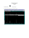
1
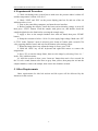
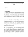
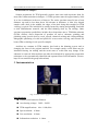
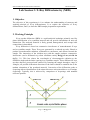
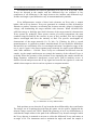
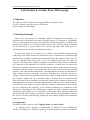
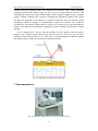
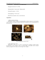
Lab Sessions Guide Advanced Methods for Materials Characterization School of Materials Science and Engineering University of Shanghai for Science and Technology (2011-2013) This page is intentionally left blank Advanced Methods for Materials Characterization Lab Sessions Guide TableofContents Preface ...........................................................ii Lab Session 1 Scanning Electron Microscopy .........................1 Lab Session 2 Transmission Electron Microscopy .....................5 Lab Session 3 X-ray Diffraction ....................................9 Lab Session 4 Atomic Force Microscopy .............................13 Lab Session 5 Ultraviolet-visible Spectroscopy ....................18 Lab Session 6 Raman spectroscopy ..................................22 Lab Session 7 Differential Scanning Calorimetry ...................24 Lab Session 8 Electrical Properties ...............................27 i Advanced Methods for Materials Characterization Lab Sessions Guide Preface This brochure is prepared as a ‘Lab Sessions Guide’ for the course of ‘Advanced Methods for Materials Characterization’, which is one of the core courses for undergraduate students in the School of Materials Science and Engineering, University of Shanghai for Science and Technology (USST). In this course, students are expected to explore the beauty and scientific significance of a number of experimental approaches frequently used in the fields of materials science and engineering as well as physics, chemistry, biology and related disciplines. The principal goal of this guide is to offer the students step-by-step instruments during the lab sessions, nonetheless, it may also be helpful to our colleagues and graduate students for their research purpose as an abridged manual of the apparati included. We are greatly indebted to our colleagues, Drs. Xiao-Hong Chen, Hui-Juan Zhang, Sheng-Juan Li, for their wonderful help during preparation of this guide. We also wish to thank Profs. Junhe Yang, Fang Liu, Xia Wang and Fengcang Ma for their encouragement and constructive suggestions to make this course possible. Thanks are also due to the authors of the original materials we referenced herein. Deng Pan Dunliang Jian Xianying Wang ii Advanced Methods for Materials Characterization Lab Sessions Guide Lab Session 1: Scanning Electron Microscopy (SEM) 1. Objective The objective of this experiment is 1) to enhance the understanding of structure and working principle of SEM; 2) to observe the morphology and Z contrast of specimen; and 3) to explore the spatial resolution of an SEM. 2. Working Principle In some ways, SEMs work in the same way key copying machines work. When you get a key copied at your local hardware store, a machine traces over the indentations of the original key while cutting an exact replica into a blank key. The copy isn't made all at once, but rather traced out from one end to the other. You might think of the specimen under examination as the original key. The SEM's job is to use an electron beam to trace over the object, creating an exact replica of the original object on a monitor. So rather than just tracing out a flat one-dimensional outline of the key, the SEM gives the viewer more of a living, breathing 3-D image, complete with grooves and engraving. As the electron beam traces over the object, it interacts with the surface of the object, dislodging secondary electrons from the surface of the specimen in unique patterns. A secondary electron detector attracts those scattered electrons and, depending on the number of electrons that reach the detector, registers different levels of brightness on a monitor. Additional sensors detect backscattered electrons (electrons that reflect off the specimen's surface) and X-rays (emitted from beneath the specimen's surface). Dot by dot, row by row, an image of the original object is scanned onto a monitor for viewing (hence the "scanning" part of the machine's name). Of course, this entire process wouldn't be possible if the microscope couldn't control the movement of an electron beam. SEMs use scanning coils, which create a magnetic field using fluctuating voltage, to manipulate the electron beam. The scanning coils are able to move the beam precisely back and forth over a defined section of an object. If a researcher wants to increase the magnification of an image, he or she simply sets the electron beam to scan a smaller area of the sample. While it's nice to know how an SEM works in theory, operating one is even better. Key Components of an SEM Electron gun: Electron guns aren't some futuristic weapon used in the newest Vin Diesel movie. Instead, they produce the steady stream of electrons necessary for SEMs to operate. Electron guns are typically one of two types. Thermionic guns, which are the most common type, apply thermal energy to a filament (usually made of tungsten, which has a high melting point) to coax electrons away from the gun and toward the specimen under examination. Field emission guns, on the other hand, create a strong electrical field to pull electrons away from the atoms they're associated with. Electron 1 Advanced Methods for Materials Characterization Lab Sessions Guide guns are located either at the very top or at the very bottom of an SEM and fire a beam of electrons at the object under examination. These electrons don't naturally go where they need to, however, which gets us to the next component of SEMs. Fig. 1-1 Schematic of SEM key components Lenses: Just like optical microscopes, SEMs use lenses to produce clear and detailed images. The lenses in these devices, however, work differently. For one thing, they aren't made of glass. Instead, the lenses are made of magnets capable of bending the path of electrons. By doing so, the lenses focus and control the electron beam, ensuring that the electrons end up precisely where they need to go. Sample chamber: The sample chamber of an SEM is where researchers place the specimen that they are examining. Because the specimen must be kept extremely still for the microscope to produce clear images, the sample chamber must be very sturdy and insulated from vibration. In fact, SEMs are so sensitive to vibrations that they're often installed on the ground floor of a building. The sample chambers of an SEM do more than keep a specimen still. They also manipulate the specimen, placing it at different angles and moving it so that researchers don't have to constantly remount the object to take different images. Detectors: You might think of an SEM's various types of detectors as the eyes of the microscope. These devices detect the various ways that the electron beam interacts with the sample object. For instance, Everhart-Thornley detectors register secondary electrons, which are electrons dislodged from the outer surface of a specimen. These detectors are capable of producing the most detailed images of an object's surface. Other detectors, such as backscattered electron detectors and X-ray detectors, can tell researchers about the composition of a substance. Vacuum chamber: SEMs require a vacuum to operate. Without a vacuum, the 2 Advanced Methods for Materials Characterization Lab Sessions Guide electron beam generated by the electron gun would encounter constant interference from air particles in the atmosphere. Not only would these particles block the path of the electron beam, they would also be knocked out of the air and onto the specimen, which would distort the surface of the specimen. (Source: www.howstuffworks.com) 3. Instrumentation Fig. 1-2 QUANTA FEG450 SEM equipped with field emission gun Specifications: 1. Secondary Electron resolution: High vacuum mode: 1.2nm (30kV) Low vacuum mode: 1.4nm (30kV) Back scattering electron resolution: 2.5nm (30kV) Accelerating voltage: 0.2kV-30kV Magnification range: 12x – 1,000,000x Current: 200nA max. 2. Sample Chamber Sample stage: 5-axis servo auto-centering stage X≥100mm Y≥100mm Z≥100mm T≥-5~+70° R=360°continuous rotation Sample Size: horizontal length >280mm 3 Advanced Methods for Materials Characterization Lab Sessions Guide 4. Experimental Procedure 1. Check circulating water system first to make sure the pressure index is about 4.5 and the temperature is about 18 to 20 oC. 2. Check ‘LINE’ and ‘INV’ on the power display panel are lit, and one of the six indicators above is on. 3. Turn on the controlling computer, and start the user interface. 4. Before loading the sample, check the beam on/accelerating voltage is turn off, then press ‘VENT’ button. Load the sample with gloves on, and double check the sample height below the limit before securing the sample stage. 5. Apply a force to the sample chamber door with one hand, then press ‘PUMP’ button. 6. Pump the vacuum to below <5x10⁻³ Pa, then apply high voltage. Make sure ‘SE’ or ‘TLD’ in the ‘Detector’ menu is selected, press ‘beam on’ button, then a sound of V6 valve opening shall be heard, and wait for the button color turning yellow. 7. When the image shows up, adjust the image in focus, press ‘OK’. 8. Hold left ‘Shift’ key on the keyboard and right-click mouse to remove the astigmatism. 9. Press ‘F6’ to scan the image frame, then save the image by selecting ‘Save As…’ in the ‘File’ pulldown menu. 10. After the session is done, press ‘beam on’ button then wait a few seconds for the V6 valve sound, button color turns to gray from yellow, then pump the air into the sample chamber, remove the sample, then restore the chamber vacuum. 5. Other Requirements Other requirements for this lab session and lab report will be delivered by the instructor at the session. 4 Advanced Methods for Materials Characterization Lab Sessions Guide Lab Session 2: Transmission Electron Microscopy (TEM) 1. Objective The objective of this experiment is 1) to enhance the understanding of structure and working principle of TEM; and 2) to explore the spatial resolution of a TEM. 2. Working Principle The transmission electron microscope uses a high energy electron beam transmitted through a very thin sample to image and analyze the microstructure of materials with atomic scale resolution. The electrons are focused with electromagnetic lenses and the image is observed on a fluorescent screen, or recorded on film or digital camera. The electrons are accelerated at several hundred kV, giving wavelengths much smaller than that of light: 200kV electrons have a wavelength of 0.025Å. However, whereas the resolution of the optical microscope is limited by the wavelength of light, that of the electron microscope is limited by aberrations inherent in electromagnetic lenses, to about 1-2 Å. Because even for very thin samples one is looking through many atoms, one does not usually see individual atoms. Rather the high resolution imaging mode of the microscope images the crystal lattice of a material as an interference pattern between the transmitted and diffracted beams. This allows one to observe planar and line defects, grain boundaries, interfaces, etc. with atomic scale resolution. The brightfield/darkfield imaging modes of the microscope, which operate at intermediate magnification, combined with electron diffraction, are also invaluable for giving information about the morphology, crystal phases, and defects in a material. Finally the microscope is equipped with a special imaging lens allowing for the observation of micromagnetic domain structures in a field-free environment. The TEM is also capable of forming a focused electron probe, as small as 20 Å, which can be positioned on very fine features in the sample for microdiffraction information or analysis of x-rays for compositional information. The latter is the same signal as that used for EMPA and SEM composition analysis (see EMPA facility), where the resolution is on the order of one micron due to beam spreading in the bulk sample. The spatial resolution for this compositional analysis in TEM is much higher, on the order of the probe size, because the sample is so thin. Conversely the signal is much smaller and therefore less quantitative. The high brightness field-emission gun improves the sensitivity and resolution of x-ray compositional analysis over that available with more traditional thermionic sources. 5 Advanced Methods for Materials Characterization Lab Sessions Guide Restrictions on Samples: Sample preparation for TEM generally requires more time and experience than for most other characterization techniques. A TEM specimen must be approximately 1000 Å or less in thickness in the area of interest. The entire specimen must fit into a 3mm diameter cup and be less than about 100 microns in thickness. A thin, disc shaped sample with a hole in the middle, the edges of the hole being thin enough for TEM viewing, is typical. The initial disk is usually formed by cutting and grinding from bulk or thin film/substrate material, and the final thinning done by ion milling. Other specimen preparation possibilities include direct deposition onto a TEM-thin substrate (Si3N4, carbon); direct dispersion of powders on such a substrate; grinding and polishing using special devices (t-tool, tripod); chemical etching and electropolishing; lithographic patterning of walls and pillars for cross-section viewing; and focused ion beam (FIB) sectioning for site specific samples. Artifacts are common in TEM samples, due both to the thinning process and to changing the form of the original material. For example surface oxide films may be introduced during ion milling and the strain state of a thin film may change if the substrate is removed. Most artifacts can either be minimized by appropriate preparation techniques or be systematically identified and separated from real information. (Source: http://www.stanford.edu/group/snl/tem.htm) 3. Instrumentation Fig. 2-1 TF30 TEM equipped with field emission gun Specifications: Schottky field emission filament Accelerating voltage:50kV-300kV TEM magnifications:60x-1000,000x Spot resolution:0.20nm Line resolution:0.10nm Information resolution:0.14nm 6 Advanced Methods for Materials Characterization Lab Sessions Guide Minimum beam spot:0.3nm Maximum angle of convergence: 12o STEM magnifications:50x-3000,000x(+8x zoom) STEM image resolution:0.17nm Max. tilting angle of sample stage: 40o Elements scope of EDX:5B-92U Working modes: Bright/dark field imaging High resolution TEM Energy dispersive spectroscopy (EDX) Selected-area electron diffraction (SAED) Scanning transmission electron microscopy (STEM) STEM-EDX 4. Experimental Procedure (1) System routine inspection a. Indicators on the control panel: ‘On’ off, ‘Off’, ‘Vac’ and ‘HT’ On; b. Sample stage indicator: off; c. Air conditioner, cooling water system, air pump, UPS and other accessories; d. Logbook. e. In ‘Tecnai User Interface’, check ‘Column Valves Closed’ to be closed(yellow), check vacuum status and sample stage position. (2) Specimen loading Refer to the user manual (this task should be done by the instructor). (3) Sample holder loading a. Set x, y, z, A, and B of the specimen to be nearly zero and the red indicator of sample stage to be off by clicking ‘Holder’; b. Push the sample holder into position without any holder rotation; c. Select ‘single tilt sample holder’; d. Click ‘Turbo On’ to shut down the turbine pump. (4) Software loading a. Load ‘Tecnai User Interface’; b. Load ‘DigitalMicrograph’; c. Load ‘ESVision.exe’ and ‘RTEM’ when EDX is required. (5) Set the eucentric height (6) Adjust condenser astigmatism (7) Morphology observation and Imaging Acquisition 7 Advanced Methods for Materials Characterization Lab Sessions Guide a. Select interested area with trace ball; b. Select proper magnification with ‘Magnification’ knob; c. Select proper step size with ‘Focus’ button; d. Adjust the contrast to minimum; e. Press ‘L1’; f. Click ‘search’ to scan; g. Adjust the focus to its best; h. Click ‘Acquire’ to obtain the image; i. Save the image. 5. Other Requirements Other requirements for this lab session and lab report will be delivered by the instructor at the session. 8 Advanced Methods for Materials Characterization Lab Sessions Guide Lab Session 3: X-Ray Diffractometry (XRD) 1. Objective The objective of this experiment is 1) to enhance the understanding of structure and working principle of X-ray diffractometer; 2) to explore the capacities of X-ray diffractometer; and 3) to learn the XRD sample preparation requirements. 2. Working Principle X-ray powder diffraction (XRD) is a rapid analytical technique primarily used for phase identification of a crystalline material and can provide information on unit cell dimensions. The analyzed material is finely ground, homogenized, and average bulk composition is determined. X-ray diffraction is based on constructive interference of monochromatic X-rays and a crystalline sample. These X-rays are generated by a cathode ray tube, filtered to produce monochromatic radiation, collimated to concentrate, and directed toward the sample. The interaction of the incident rays with the sample produces constructive interference (and a diffracted ray) when conditions satisfy Bragg's Law (nλ=2d sin θ)(Fig. 3.1). This law relates the wavelength of electromagnetic radiation to the diffraction angle and the lattice spacing in a crystalline sample. These diffracted X-rays are then detected, processed and counted. By scanning the sample through a range of 2θangles, all possible diffraction directions of the lattice should be attained due to the random orientation of the powdered material. Conversion of the diffraction peaks to d-spacings allows identification of the mineral because each mineral has a set of unique d-spacings. Typically, this is achieved by comparison of d-spacings with standard reference patterns. Fig. 3-1 Bragg Law 9 Advanced Methods for Materials Characterization Lab Sessions Guide All diffraction methods are based on generation of X-rays in an X-ray tube. These X-rays are directed at the sample, and the diffracted rays are collected. A key component of all diffraction is the angle between the incident and diffracted rays. Powder and single crystal diffraction vary in instrumentation beyond this. X-ray diffractometers consist of three basic elements: an X-ray tube, a sample holder, and an X-ray detector. X-rays are generated in a cathode ray tube by heating a filament to produce electrons, accelerating the electrons toward a target by applying a voltage, and bombarding the target material with electrons. When electrons have sufficient energy to dislodge inner shell electrons of the target material, characteristic X-ray spectra are produced. These spectra consist of several components, the most common being Kα and Kβ. Kα consists, in part, of Kα1 and Kα2. Kα1 has a slightly shorter wavelength and twice the intensity as Kα2. The specific wavelengths are characteristic of the target material (Cu, Fe, Mo, Cr). Filtering, by foils or crystal monochrometers, is required to produce monochromatic X-rays needed for diffraction. Kα1and Kα2 are sufficiently close in wavelength such that a weighted average of the two is used. Copper is the most common target material for single-crystal diffraction, with CuKα radiation = 1.5418Å. These X-rays are collimated and directed onto the sample. As the sample and detector are rotated, the intensity of the reflected X-rays is recorded. When the geometry of the incident X-rays impinging the sample satisfies the Bragg Equation, constructive interference occurs and a peak in intensity occurs. A detector records and processes this X-ray signal and converts the signal to a count rate which is then output to a device such as a printer or computer monitor. Fig. 3-2 Schematic of X-ray diffractometer Peak positions occur where the X-ray beam has been diffracted by the crystal lattice. The unique set of d-spacings derived from this patter can be used to 'fingerprint' the mineral. Image courtesy the USGS. DetailsThe geometry of an X-ray diffractometer is such that the sample rotates in the path of the collimated X-ray beam at an angle θ while the X-ray detector is mounted on an arm to collect the diffracted X-rays and rotates at an angle of 2θ. The instrument used to maintain the angle and rotate the sample is 10 Advanced Methods for Materials Characterization Lab Sessions Guide termed a goniometer. For typical powder patterns, data is collected at 2θ from ~5° to 70°, angles that are preset in the X-ray scan. 3. Experimental Procedure 1. Turn on the power of the units in the following sequence: master power supplycooling water systemX-ray diffractometercomputer; 2. Load software ‘Pmgr’ and open three windows: ‘system parameters’, ‘testing conditions’ and ‘testing’; 3. Load the specimen to the sample stage, and close the front shields; 4. Click ‘start’ to turn on X-ray tube high voltage (‘X-rays on’ indicator at the lower left corner on) and the scan; 5. X-ray tube will be automatically turn off when scan is finished. Repeat 3-5 if multiple specimens are to be scanned. 6. When session is finished, close the windows following ‘first open, last close’ rule, then turn off the power of diffractometer and cooling water system at least 15minutes after ‘X-rays on’ indicator is off. 4. Lab Report The spectrum as shown below is obtained in an XRD experiment. Please specify the testing conditions. 11 Advanced Methods for Materials Characterization Lab Sessions Guide In your report, describe the capacities of x-ray diffractometry and its sample requirements as well as the information in the peak positions, peak width, peak area as well as peak shape. 12 Advanced Methods for Materials Characterization Lab Sessions Guide Lab Session 4: Atomic Force Microscopy 1. Objective The objective of this experiment is to gain hands-on experience with (1) Use of atomic force microscope (AFM), and (2) Processing of AFM images. 2. Working Principle Atomic force microscopy is a technique capable of imaging the morphology of a specimen with a horizontal and vertical resolution down to a fraction of a nanometer (10-9 m). The instrument works by measuring the deflection produced by a sharp tip on micron-sized cantilever as it scans across the surface of the specimen. Sample sizes that can be handled by a typical atomic force microscopy range from small pieces of sub-millimeter scale to wafers of centimeter diameter. An atomically sharp tip is scanned over a surface with feedback mechanisms that enable the piezo-electric scanners to maintain the tip at a constant force (to obtain height information), or height (to obtain force information) above the sample surface (Fig. 4-1). Tips are typically made from Si3N4 or Si, and extended down from the end of a cantilever. The nanoscope AFM head employs an optical detection system in which the tip is attached to the underside of a reflective cantilever. A diode laser is focused onto the back of a reflective cantilever. As the tip scans the surface of the sample, moving up and down with the contour of the surface, the laser beam is deflected off the attached cantilever into a dual element photodiode. The photodetector measures the difference in light intensities between the upper and lower photodetectors, and then converts to voltage. Feedback from the photodiode difference signal, through software control from the computer, enables the tip to maintain either a constant force or constant height above the sample. In the constant force mode the piezo-electric transducer monitors real time height deviation. In the constant height mode the deflection force on the sample is recorded. The latter mode of operation requires calibration parameters of the scanning tip to be inserted in the sensitivity of the AFM head during force calibration of the microscope. Depending on the AFM design, scanners are used to translate either the sample under the cantilever or the cantilever over the sample. By scanning in either way, the local height of the sample is measured. Three dimensional topographical maps of the surface are then constructed by plotting the local sample height versus horizontal probe tip position. Scanning Modes The AFM typically scans on either Tapping Mode or Contact Mode: i) ‘Tapping mode’ imaging is implemented in ambient air by oscillating the cantilever assembly at or near the cantilever's resonant frequency using a piezoelectric 13 Advanced Methods for Materials Characterization Lab Sessions Guide crystal. The piezo motion causes the cantilever to oscillate with a high amplitude (typically greater than 20nm) when the tip is not in contact with the surface. The oscillating tip is then moved toward the surface until it begins to lightly touch, or tap the surface. During scanning, the vertically oscillating tip alternately contacts the surface and lifts off, generally at a frequency of 50,000 to 500,000 cycles per second. As the oscillating cantilever begins to intermittently contact the surface, the cantilever oscillation is necessarily reduced due to energy loss caused by the tip contacting the surface. The reduction in oscillation amplitude is used to identify and measure surface features. ii) In ‘contact mode’, the tip scans the sample in close contact with the surface, which is the common mode used in the force microscope. The force on the tip is repulsive with a mean value of 10-9 N. This force is set by pushing the cantilever against the sample surface with a piezoelectric positioning element. Fig. 4-1 Schematic of AFM working principle 3. Instrumentation Fig. 4-2 Shimadzu SPM-9500-J3 Atomic Force Microscope 14 Advanced Methods for Materials Characterization AFM model: Lab Sessions Guide SHIMADZU(岛津) SPM-9500J3 Imaging Environment: Air, Fluid Scanning Mode: Contact mode; Tapping mode Scanning Frequency: 1-10 Hz Scanning Range: 125*125 m2 Resolution: horizontal 0.1nm; vertical 0.01nm Capabilities: 1. High-resolution Imaging: SPM-9500J3 AFM is capable of capturing high-resolution images in a environment of air or fluid to investigate structure-properties correlation in situ and dynamically at molecular level. Fig. 4-3 AFM high-resolution images 2. Tip-sample force curves SPM-9500J3 AFM may be used for measuring the bonding strength among bio-molecules in the solution, such as covalent bonds, electrostatic force, friction, elasticity, magnetic force and so on. See Fig.4-4 for example. 15 Advanced Methods for Materials Characterization Lab Sessions Guide Fig. 4-4 AFM tip-sample force curves (Ref: http://www.antpedia.com/labs/641/101/) 4. Experimental Procedure 1. Turn on the power of the units in the following sequence: computerSPM control unitmonitorprinter. 2. Double click the shortcut ‘SPM Manager’ on the desktop to start the software; click ‘online’ button when the ‘ready’ indicator on the SPM control unit is lit, then make sure ‘standby’ is shown at the bottom of the window. 3. Mount the specimen at the center of the sample stage with double-side tape or glue. The specimen size shall not be greater than 24mm in diameter and 8mm in height. 4. Check whether there is sufficient space for the specimen between the cantilever and the sample stage. If more space is needed, click ‘Menu-level-up’ till enough space is obtained, then click ‘Menu-level-stop’. 5. Loose the claps of the AFM head then slide backward for location of sample stage. Locate the sample stage in position then slide the AFM slide forward, lock the AFM head. 6. In the pulldown menu ‘settings’, select ‘mode and scanner’ ‘dynamic mode’, click ‘OK’. 7. In the pulldown menu ‘settings’, select ‘panel display’. Adjust laser control knobs in the x-y plane to focus the laser point at the cantilever tip (2-4 lights in the digital signal panel). Set ‘operating point’ in ‘scan condition’ to 0, then adjust detector settings to set LED display to 0. Select ‘vertical RMS’ for ‘panel display’. 8. In the pulldown menu ‘settings’, select ‘level tune’. ‘auto’ adjust frequency to close the gap between blue frequency indicator and red piezo-ceramic frequency indicator, then click ‘OK’. 9. Click ‘fast approach’ in the toolbar, then check the signal panel to make sure LED display to be in the range of -0.01 to -0.06. If out of range, adjust ‘operating point’ on the ‘scan condition’ panel to adjust the value in LED display. 10. Click ‘file save this/save next’ in the toolbar, fill in the specimen information, 16 Advanced Methods for Materials Characterization Lab Sessions Guide then click ‘OK’. 11. Click ‘offline’ button in the ‘SPM manager’ to eliminate the background and noise signal in the data. Save the reduced image in a file or a MS-word document. 5. Lab Report You are required to submit a lab report in which the following sections should be included: Title Page: This should include title of lab session, date of the lab session, your name and student ID, and date of report submission. Introduction: This section should be brief and should explain the scope of the project (general purpose) as well as some of the methodology used in this lab session. This should be no more than 200 words. Experimental Section: This should give a more detailed description of the actual procedural steps taken during the session. This should be in enough detail (but in your own words) that your report reader may follow your description to successfully reproduce your results. Results and Discussion: This section should contain the actual raw data obtained in the analysis. Numbers should be compiled in to tables (labeled with “Table 1”, “Table 2”, etc), and tables should be neatly organized for someone who might read your paper (namely the one grading it). All the results presented in your figures and tables shall be interpreted in full details. Calculations, if any, required to complete the analysis should be described in detail in this section. The lab report should be typed / printed. 17 Advanced Methods for Materials Characterization Lab Sessions Guide Lab Session 5: Ultraviolet-visible Spectroscopy 1. Objective The objective of this experiment is to gain hands-on experience with (1) Use of multi-channel absorption spectrophotometers, and (2) Derivative spectroscopy in chemical analysis. 2. Working Principle I. The absorption law—the Beer-Lambert Law -lg(I/Io)=εlc where Io = the intensities of the incident light I = the intensities of the transmitted light l= the path length of the absorbing in centimeters c= the concentration in moles per liter εis known as the molar extinction coefficient II. Calibration of a UV-vis Spectrometer A. Wavelength Calibration Solutions of rare earth ions exhibit very narrow absorption bands, the wavelengths of which are well known. Holmium has many peaks well spaced in wavelength which provide convenient calibration points. You will calibrate the wavelength with a sample of Holmium oxide immobilized in a polymer block. Measure the spectrum of the solution using the PE UV/Vis Photodiode Array Spectrometer. Check the apparent wavelength of the absorption peaks which should be at 287.0, 361.1, 450.8, 537.0, and 640.4 nm. Use the Peak/Spectrum function to annotate each peak, then print the entire spectrum and the wavelength report to determine the exact wavelength maxima. B. Photometric Calibration Basic potassium chromate is recommended as a photometric standard by the National Bureau of Standards. You have been given a solution containing 0.1 g/l of K2CrO4 and a solution 0.5 N in KOH, from which you prepared solutions containing 0.04, 0.03, 0.02 and 0.01 g/l K2CrO4 in 0.05 N KOH. Measure the spectra of these solutions and read the absorbance at 370 nm. Use FIXED WAVELENGTH under METHOD then specify the wavelength. To save time and paper, all the spectra can be overlaid then printed. Be sure to correct the wavelength as needed according to the results in part I.A. Check for linearity of response and also for proper slope in the response curve. The absorbance of your most concentrated solution should be 0.9914. Any relative deviation of over 1% from linearity or from the proper slope is cause for concern. 3. Instrumentation 18 Advanced Methods for Materials Characterization Lab Sessions Guide Currently, research grade UV-vis absorption instruments come in two configurations. The first is called a scanning spectrophotometer because it measures the intensity of transmitted light of a narrow band pass, and scans the wavelength in time in order to collect a spectrum. Because absorption is a radiometric measurement, these instruments generally require the user to measure two spectra, one sample and one blank. The blank should be identical to the sample in every way except that the absorbing species of interest is not present. This can be done either consecutively with a single beam instrument followed by the ratio calculation, or simultaneously with a dual beam instrument. The dual beam method is faster, and has the added advantage that lamp drift and other slow intensity fluctuations are properly accounted for in the ratio calculation. Collecting spectra with scanning spectrophotometers is slow, but the instruments often have very high resolving power owing to the use of photomultiplier tube detectors, which can be used with very narrow slit widths. A photodiode array is a 1 or 2 dimensional stack of individual photodiode detectors, each of which makes an independent measurement of the incident light intensity at its particular location. Typically, 2-dimensional arrays are used for electronic imaging applications, for instance the photo detector of a camcorder. One -dimensional arrays are often used in spectroscopic instrumentation. If the array is placed at the focal plane of a monochromatic, then the position of each photodiode will be associated with a specific bandwidth of light. In the case of the diode array spectrograph that we will use for the UV-vis experiment each of 1024 diodes in the linear array is associated with a 1 nm band of light spanning from 190 nm to 2500 nm. The individual diodes are separated by about 25 microns, and the physical slit width matches this spacing. Thus the maximum resolution of the instrument is 1 nm. This is not as good as the typical resolution of a scanning instrument (resolutions of about 0.2nm are not uncommon with scanning instruments), but for many applications (especially molecular solution spectroscopy where absorption bands are typically very broad) 1 nm is adequate. The real advantage of the instrument is its speed. A single spectrum can be taken in about 0.1 seconds. 4. Experimental Procedure Preliminary Preparations Before turn the instrument so that the light sources have a chance to warm up and stabilize. Next prepare or gather all of the samples which you will need to perform the experiment. Solutions which students need to prepare are marked with *. *1. a) Solutions containing 100 ppm of indicator (Phenolphthalein,methyl orange etc) in water as a stock solution b) Water blank Derivative Spectroscopy and Quantitative Analysis 19 Advanced Methods for Materials Characterization Lab Sessions Guide This Lambd750 performs derivative spectroscopy by measuring the actual spectrum and performing the derivative operations in the computer. It is capable of 1st through 4th derivatives, though only 1st and 2nd derivatives are used regularly. The advantages of derivative spectroscopy include: (1) Precise determination of the wavelength of peak maxima can be obtained from the zero crossing of the first derivative. (2) Improved spectral resolution is obtained, especially with the second derivative. Spectral features which appear as barely noticeable shoulders in the original spectrum become much more prominent. (3) Quantitative analysis can be performed in the presence of turbidity. Turbid solution generally shows steadily increasing absorbance toward shorter wavelength, which can hinder the accurate measurement of absorbance due to the changing background level. One solution to this problem is to calculate the expected background and subtract it off. Another approach is to calculate the spectrum's second derivative. A. indicator standard solutions (with water blanks) Measure the spectrum of 1.0, 5.0, and 10 ppm MO in water solutions. Measure, mark, and print the absorbance and the 1st and the 2nd derivative spectra of these. During the lab exercise, ALL OBSERVATIONS SHOULD BE RECORDED IN YOUR LAB NOTEBOOK! 5. Lab Report You are required to submit a lab report in which the following sections should be included: Title Page: This should include the name of the lab, the student’s name, date the lab was performed, the phenol unknown number and determined concentration of the unknown with an uncertainty assignment, and the date the paper is submitted for grading. Introduction: This section should be brief and should explain the scope of the project (general purpose) as well as some of the methodology used in the lab. This should be no more than 200 words, but should be thorough enough to give some idea as to what the rest of the paper will cover. This lab covers a phenol unknown determination and some calibration experiments. Experimental Section: This should give a more detailed description of the actual procedural steps taken during the lab. This should be in enough detail (but in the student’s own words) that someone reading the paper would be able to exactly reproduce the experiment that YOU performed. Results/Raw Data: This section should contain the actual raw data obtained in the analysis. Numbers should be compiled in to tables (labeled with “Table 1”, “Table 2”, etc), and tables should be neatly organized for someone who might read your paper (namely the one grading it). This section should not contain explanations or 20 Advanced Methods for Materials Characterization Lab Sessions Guide interpretations of the data. Data Analysis: This is the main text of the report. This should contain any figures, graphs, calibration plots and explanations that might help the reader in interpreting the data presented in the Results/Raw Data section. This is where you will present your calibration plots and your error analysis. Any calculations required to complete the analysis should be described in detail in this section. The lab report should be typed/printed. Questions: Answer the following questions in this section: 1. What effect would drift caused by a gradual increase in source intensity have on a measurement of absorbance versus time in a single beam spectrometer? How is this accounted for in the instruments used in this experiment? 2. What effect would an error in cell dimensions (say 10.50 mm instead of 10.00 mm) have on the value of ε (assuming A and c are constant)? 3. Why use a rare earth ion for wavelength calibration? 4. What are the advantages and disadvantages of using derivative spectroscopy? 21 Advanced Methods for Materials Characterization Lab Sessions Guide Lab Session 6: Raman Spectroscopy 1. Objective The objective of this experiment is 1) to enhance the understanding of structure and working principle of Raman spectroscopy; and 2) to get familiar with investigation of powder materials by Raman spectroscopy. 2. Working Principle The principle of the Raman spectroscopy is relatively simple. It consists in sending a monochromatic light (only one color and not a mixture) on the sample to study and analyze the scattered light. The scattering process is the following: the incidental photons are destroyed and their energy is used for creating scattered photons and creating (Stokes process) or destroying (anti-Stokes process) vibrations in the studied sample. This can be modelized in the following way (Stokes process): Two types of rules govern this process: the conservation of energy which is represented on the preceding drawing and also rules of symmetry which depend on studied material. From a practical point of view, to carry out an experiment of Raman scattering, it is necessary to focus light (in general a laser) on the sample to be studied using a lens. Then the scattered light is collected using another lens and is sent in a monochromator, then its intensity is measured using a photomultiplier. The scattered light is generally detected in a different direction than that of the light reflected by the sample, except when carrying experiments under a microscope. (Source: http://pcml.univ-lyon1.fr/raman/raman_eng.html) 3. Instrumentation Fig. 6-1 RamanStation™ 400F spectrometer (with optic fiber) 22 Advanced Methods for Materials Characterization Lab Sessions Guide 4. Experimental Procedure 1. Turn on the power of the units in the following sequence: computerRaman spectroscope. 2. Load software ‘Pyris’, and set up testing parameters such as wavelength range and scan times. 3. Mount the sample onto a glass slide, load the slide into the spectroscope, then close the cover. 4. Click ‘auto focus’ to tune the optical path, then click ‘scan’ after the image is in focus. 5. After all the scans are done, save the data. 6. Unload the sample slide, close the cover. 7. Shut down the spectroscope and the computer. 5. Other Requirements Other requirements for this lab session and lab report will be delivered by the instructor at the session. 23 Advanced Methods for Materials Characterization Lab Sessions Guide Lab Session 7: Differential Scanning Calorimetry (DSC) 1. Objective The objective of this experiment is 1) to enhance the understanding of structure and working principle of differential scanning calorimetry (DSC); and 2) to get familiar with routine testing procedure of DSC. 2. Working Principle Differential scanning calorimetry (DSC) monitors heat effects associated with phase transitions and chemical reactions as a function of temperature. In a DSC the difference in heat flow to the sample and a reference at the same temperature, is recorded as a function of temperature. The reference is an inert material such as alumina, or just an empty aluminum pan. The temperature of both the sample and reference are increased at a constant rate. Since the DSC is at constant pressure, heat flow is equivalent to enthalpy changes. In an endothermic process, such as most phase transitions, heat is absorbed and, therefore, heat flow to the sample is higher than that to the reference. Hence ΔdH/dt is positive. Other endothermic processes include helix-coil transitions in DNA, protein denaturation, dehydrations, reduction reactions, and some decomposition reactions. In an exothermic process, such as crystallization, some cross-linking processes, oxidation reactions, and some decomposition reactions, the opposite is true and ΔdH/dt is negative. The calorimeter consists of a sample holder and a reference holder. Both are constructed of platinum to allow high temperature operation. Under each holder is a resistance heater and a temperature sensor. Currents are applied to the two heaters to increase the temperature at the selected rate. The difference in the power to the two holders, necessary to maintain the holders at the same temperature, is used to calculate ΔdH/dt . 24 Advanced Methods for Materials Characterization Lab Sessions Guide 3. Instrumentation Fig. 7-1 Perkin-Elmer Pyris Differential Scanning Calorimeter 4. Experimental Procedure 1. 2. 3. 4. Open the gas flows and adjust to required flow rates. Turn on the power of the units in the following sequence: computerDSC. Load software ‘Pyris’, then select DSC and wait for green ‘Ready’ indicator on. Weigh proper amount of sample (melting point testing: 3-5mg; glass transition: 5-10mg) then load the sample into the aluminum pan, seal the sample in good contact with the pan. 5. Make sure that the sample and reference holders are empty. Place the vented platinum covers into the sample and reference holders. Close and secure the sample holder enclosure cover. 6. From the ‘File’ menu, select ‘Method Editor’. In the ‘Sample Info’ tab, fill in sample information and testing parameters. 7. In the Method Editor, fill in the sample weight, then wait for the temperature reach initial testing temperature, press button to start the measurement. 8. After all the scans are done, save the data. 9. Unload the sample and reference pans, turn off the heater. 10. Shut down the DSC and the computer, and keep the protective gas on for another 5 hours. 5. Other Requirements Sample preparation: a. Keep the sample as thin as possible; b. Cover as much of the pan bottom as possible; 25 Advanced Methods for Materials Characterization Lab Sessions Guide c. Cut, rather than crush, the sample. Heating rate: Keep the heating rate in the range of 10-20 oC/min. Protective gas: Use high-purity nitrogen or oxygen. Other requirements for this lab session and lab report will be delivered by the instructor at the session. 26 Advanced Methods for Materials Characterization Lab Sessions Guide Lab Session 8: Electrical Properties 1. Objective The objective of this experiment is 1) to enhance the understanding of structure and working principle of probe station and parameter analyzer; and 2) to acquire I-V curve of a specimen for calculation its electrical conductance. 2. Working Principle In this session, a Cascade M150 probe station and Keithley 4200 parameter analyzer are employed for micro-scale electrical properties measurements, with a current resolution of 0.1fA and voltage resolution of 1 V. They are connected to each other by 3-axis cables. 3. Instrumentation Fig. 8-1 Probe station Fig. 8-2 Parameter analyzer 4. Experimental Procedure 1. Turn on the power of the units in the following sequence: microscopevacuum pumpparameter analyzerCCD controlling computer. 2. Make sure all the cable connections and probe tip are properly installed. 3. Mount the sample at the center of specimen stage by applying vacuum, adjust microscope to observe the sample. 4. Adjust probe tip position in connection with one electrode of the sample and under microscope observation. 5. Lower the probe tip till in focus under the microscope and CCD camera. 6. Repeat 4 and 5 for the other probe tip. 7. Load Keithley 4200 parameter analyzer software as shown in Fig 8-3. 27 Advanced Methods for Materials Characterization Lab Sessions Guide Fig. 8-3 Keithley 4200 software 8. The data acquisition process is as follows: In KITE, select File -> New Project. A “Define New Project” window will open Name the project (up to 260 characters including directory path, no spaces) Specify location (or accept default location C:\S4200\kiuser\Projects\) Specify number of sites (up to 999) Turn ON or OFF the Project Plan Initialization and Termination Steps, click OK to accept Insert new Subsite Plan(s) Insert new Device Plan(s) – from a toolbar menu, or using Device Library To use Device Library, double-click on the Subsite Plan, then use Copy and Submit buttons To use Test Library, double-click on the Device Plan, then use Copy and Submit buttons Under User Libraries, select KI42xxulib Under User Modules, select Rdson42xx Enter / modify user parameters Save module Execute the UTM by clicking the Run button View the results in the Data tab Create another UTM using the Matrixulib library and the ConnectPins module When done building project, select File -> Save All To create a copy of the project under a different name, select File -> Save Project As… 9. Lift up the probe tip 10. Shut down the power of all the components. 28 Advanced Methods for Materials Characterization Lab Sessions Guide 5. Other Requirements Other requirements for this lab session and lab report will be delivered by the instructor at the session. 29