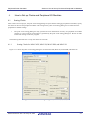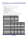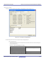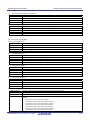
1
To our customers,
Old Company Name in Catalogs and Other Documents
On April 1st, 2010, NEC Electronics Corporation merged with Renesas Technology
Corporation, and Renesas Electronics Corporation took over all the business of both
companies. Therefore, although the old company name remains in this document, it is a valid
Renesas Electronics document. We appreciate your understanding.
Renesas Electronics website: http://www.renesas.com
April 1st, 2010
Renesas Electronics Corporation
Issued by: Renesas Electronics Corporation (http://www.renesas.com)
Send any inquiries to http://www.renesas.com/inquiry.
Notice
1.
2.
3.
4.
5.
6.
7.
All information included in this document is current as of the date this document is issued. Such information, however, is
subject to change without any prior notice. Before purchasing or using any Renesas Electronics products listed herein, please
confirm the latest product information with a Renesas Electronics sales office. Also, please pay regular and careful attention to
additional and different information to be disclosed by Renesas Electronics such as that disclosed through our website.
Renesas Electronics does not assume any liability for infringement of patents, copyrights, or other intellectual property rights
of third parties by or arising from the use of Renesas Electronics products or technical information described in this document.
No license, express, implied or otherwise, is granted hereby under any patents, copyrights or other intellectual property rights
of Renesas Electronics or others.
You should not alter, modify, copy, or otherwise misappropriate any Renesas Electronics product, whether in whole or in part.
Descriptions of circuits, software and other related information in this document are provided only to illustrate the operation of
semiconductor products and application examples. You are fully responsible for the incorporation of these circuits, software,
and information in the design of your equipment. Renesas Electronics assumes no responsibility for any losses incurred by
you or third parties arising from the use of these circuits, software, or information.
When exporting the products or technology described in this document, you should comply with the applicable export control
laws and regulations and follow the procedures required by such laws and regulations. You should not use Renesas
Electronics products or the technology described in this document for any purpose relating to military applications or use by
the military, including but not limited to the development of weapons of mass destruction. Renesas Electronics products and
technology may not be used for or incorporated into any products or systems whose manufacture, use, or sale is prohibited
under any applicable domestic or foreign laws or regulations.
Renesas Electronics has used reasonable care in preparing the information included in this document, but Renesas Electronics
does not warrant that such information is error free. Renesas Electronics assumes no liability whatsoever for any damages
incurred by you resulting from errors in or omissions from the information included herein.
Renesas Electronics products are classified according to the following three quality grades: “Standard”, “High Quality”, and
“Specific”. The recommended applications for each Renesas Electronics product depends on the product’s quality grade, as
indicated below. You must check the quality grade of each Renesas Electronics product before using it in a particular
application. You may not use any Renesas Electronics product for any application categorized as “Specific” without the prior
written consent of Renesas Electronics. Further, you may not use any Renesas Electronics product for any application for
which it is not intended without the prior written consent of Renesas Electronics. Renesas Electronics shall not be in any way
liable for any damages or losses incurred by you or third parties arising from the use of any Renesas Electronics product for an
application categorized as “Specific” or for which the product is not intended where you have failed to obtain the prior written
consent of Renesas Electronics. The quality grade of each Renesas Electronics product is “Standard” unless otherwise
expressly specified in a Renesas Electronics data sheets or data books, etc.
“Standard”:
8.
9.
10.
11.
12.
Computers; office equipment; communications equipment; test and measurement equipment; audio and visual
equipment; home electronic appliances; machine tools; personal electronic equipment; and industrial robots.
“High Quality”: Transportation equipment (automobiles, trains, ships, etc.); traffic control systems; anti-disaster systems; anticrime systems; safety equipment; and medical equipment not specifically designed for life support.
“Specific”:
Aircraft; aerospace equipment; submersible repeaters; nuclear reactor control systems; medical equipment or
systems for life support (e.g. artificial life support devices or systems), surgical implantations, or healthcare
intervention (e.g. excision, etc.), and any other applications or purposes that pose a direct threat to human life.
You should use the Renesas Electronics products described in this document within the range specified by Renesas Electronics,
especially with respect to the maximum rating, operating supply voltage range, movement power voltage range, heat radiation
characteristics, installation and other product characteristics. Renesas Electronics shall have no liability for malfunctions or
damages arising out of the use of Renesas Electronics products beyond such specified ranges.
Although Renesas Electronics endeavors to improve the quality and reliability of its products, semiconductor products have
specific characteristics such as the occurrence of failure at a certain rate and malfunctions under certain use conditions. Further,
Renesas Electronics products are not subject to radiation resistance design. Please be sure to implement safety measures to
guard them against the possibility of physical injury, and injury or damage caused by fire in the event of the failure of a
Renesas Electronics product, such as safety design for hardware and software including but not limited to redundancy, fire
control and malfunction prevention, appropriate treatment for aging degradation or any other appropriate measures. Because
the evaluation of microcomputer software alone is very difficult, please evaluate the safety of the final products or system
manufactured by you.
Please contact a Renesas Electronics sales office for details as to environmental matters such as the environmental
compatibility of each Renesas Electronics product. Please use Renesas Electronics products in compliance with all applicable
laws and regulations that regulate the inclusion or use of controlled substances, including without limitation, the EU RoHS
Directive. Renesas Electronics assumes no liability for damages or losses occurring as a result of your noncompliance with
applicable laws and regulations.
This document may not be reproduced or duplicated, in any form, in whole or in part, without prior written consent of Renesas
Electronics.
Please contact a Renesas Electronics sales office if you have any questions regarding the information contained in this
document or Renesas Electronics products, or if you have any other inquiries.
(Note 1) “Renesas Electronics” as used in this document means Renesas Electronics Corporation and also includes its majorityowned subsidiaries.
(Note 2) “Renesas Electronics product(s)” means any product developed or manufactured by or for Renesas Electronics.
User’s Manual
Peripheral Driver Generator V.1.04
User’s Manual
Rev.1.00 2009.05
Notes regarding these materials
1. This document is provided for reference purposes only so that Renesas customers may select the appropriate
Renesas products for their use. Renesas neither makes warranties or representations with respect to the
accuracy or completeness of the information contained in this document nor grants any license to any
intellectual property rights or any other rights of Renesas or any third party with respect to the information in
this document.
2. Renesas shall have no liability for damages or infringement of any intellectual property or other rights arising
out of the use of any information in this document, including, but not limited to, product data, diagrams, charts,
programs, algorithms, and application circuit examples.
3. You should not use the products or the technology described in this document for the purpose of military
applications such as the development of weapons of mass destruction or for the purpose of any other military
use. When exporting the products or technology described herein, you should follow the applicable export
control laws and regulations, and procedures required by such laws and regulations.
4. All information included in this document such as product data, diagrams, charts, programs, algorithms, and
application circuit examples, is current as of the date this document is issued. Such information, however, is
subject to change without any prior notice. Before purchasing or using any Renesas products listed in this
document, please confirm the latest product information with a Renesas sales office. Also, please pay regular
and careful attention to additional and different information to be disclosed by Renesas such as that disclosed
through our website. (http://www.renesas.com )
5. Renesas has used reasonable care in compiling the information included in this document, but Renesas
assumes no liability whatsoever for any damages incurred as a result of errors or omissions in the information
included in this document.
6. When using or otherwise relying on the information in this document, you should evaluate the information in
light of the total system before deciding about the applicability of such information to the intended application.
Renesas makes no representations, warranties or guaranties regarding the suitability of its products for any
particular application and specifically disclaims any liability arising out of the application and use of the
information in this document or Renesas products.
7. With the exception of products specified by Renesas as suitable for automobile applications, Renesas
products are not designed, manufactured or tested for applications or otherwise in systems the failure or
malfunction of which may cause a direct threat to human life or create a risk of human injury or which require
especially high quality and reliability such as safety systems, or equipment or systems for transportation and
traffic, healthcare, combustion control, aerospace and aeronautics, nuclear power, or undersea communication
transmission. If you are considering the use of our products for such purposes, please contact a Renesas
sales office beforehand. Renesas shall have no liability for damages arising out of the uses set forth above.
8. Notwithstanding the preceding paragraph, you should not use Renesas products for the purposes listed below:
(1) artificial life support devices or systems
(2) surgical implantations
(3) healthcare intervention (e.g., excision, administration of medication, etc.)
(4) any other purposes that pose a direct threat to human life
Renesas shall have no liability for damages arising out of the uses set forth in the above and purchasers who
elect to use Renesas products in any of the foregoing applications shall indemnify and hold harmless Renesas
Technology Corp., its affiliated companies and their officers, directors, and employees against any and all
damages arising out of such applications.
9. You should use the products described herein within the range specified by Renesas, especially with respect
to the maximum rating, operating supply voltage range, movement power voltage range, heat radiation
characteristics, installation and other product characteristics. Renesas shall have no liability for malfunctions or
damages arising out of the use of Renesas products beyond such specified ranges.
10. Although Renesas endeavors to improve the quality and reliability of its products, IC products have specific
characteristics such as the occurrence of failure at a certain rate and malfunctions under certain use
conditions. Please be sure to implement safety measures to guard against the possibility of physical injury, and
injury or damage caused by fire in the event of the failure of a Renesas product, such as safety design for
hardware and software including but not limited to redundancy, fire control and malfunction prevention,
appropriate treatment for aging degradation or any other applicable measures. Among others, since the
evaluation of microcomputer software alone is very difficult, please evaluate the safety of the final products or
system manufactured by you.
11. In case Renesas products listed in this document are detached from the products to which the Renesas
products are attached or affixed, the risk of accident such as swallowing by infants and small children is very
high. You should implement safety measures so that Renesas products may not be easily detached from your
products. Renesas shall have no liability for damages arising out of such detachment.
12. This document may not be reproduced or duplicated, in any form, in whole or in part, without prior written
approval from Renesas.
13. Please contact a Renesas sales office if you have any questions regarding the information contained in this
document, Renesas semiconductor products, or if you have any other inquiries.
Peripheral Driver Generator
Preface
The Peripheral Driver Generator (hereafter referred to as PDG) is a tool that supports the development of
a driver for a peripheral I/O module in a microcomputer.
The PDG, which contains peripheral I/O module API libraries, allows users to design and automatically
generate functions for calling the libraries via its user interface.
It runs on a Microsoft® Windows® operating system with an IBM PC compatible machine.
The supported microcomputers are the H8S/Tiny, SH/Tiny, H8/300H Tiny, R8C/Tiny, and M16C/Tiny
series, and main groups of the M16C/60 series. For details, refer to “Overview” in this manual.
Usage Precautions
Even though we carefully evaluate the API libraries and functions generated by the PDG, fully examine
your application on your own responsibility when using this software to develop your application.
IBM is a registered trademark of International Business Machines Corporation.
Microsoft and Windows are registered trademarks of Microsoft Corporation in the United States and other
countries.
All brand or product names used in this manual are trademarks or registered trademarks of their
respective companies or organizations.
For inquiries about the contents of this document or product,
email to your local distributor.
Renesas Tools Homepage
http://www.renesas.com/en/tools
REJ10J2018-0100 Rev.1.00 May. 29, 2009
iii
Peripheral Driver Generator
Contents
1.
2.
3.
Overview...................................................................................................................................................................1-1
1.1
PDG Features.....................................................................................................................................................1-1
1.2
PDG Project .......................................................................................................................................................1-1
1.3
Roles of the PDG ...............................................................................................................................................1-2
1.4
Operating Environment......................................................................................................................................1-2
1.5
Compiler Combinations .....................................................................................................................................1-3
1.6
API Libraries......................................................................................................................................................1-3
1.7
Main Window ....................................................................................................................................................1-4
1.7.1
Setting Details Display Window................................................................................................................1-4
1.7.2
New Setup Pattern Creation Window ........................................................................................................1-5
1.7.3
Generated File Information Window .........................................................................................................1-5
1.8
Menu ..................................................................................................................................................................1-7
1.9
Toolbar............................................................................................................................................................. 1-10
Preparation for Using the PDG ..............................................................................................................................2-1
2.1
Installing the PDG .............................................................................................................................................2-1
2.2
Setting an Editor ................................................................................................................................................2-1
2.3
Registering the PDG in the HEW ......................................................................................................................2-2
2.4
Setting HewTargetServer...................................................................................................................................2-4
How to Operate the PDG ........................................................................................................................................3-1
3.1
Developing an Application with the PDG .........................................................................................................3-1
3.2
PDG Operation Flow .........................................................................................................................................3-2
3.3
Creating/Opening a Project................................................................................................................................3-3
3.3.1
Creating a New Project ..............................................................................................................................3-3
3.3.2
Opening an Existing Project ......................................................................................................................3-6
3.3.3
Setting CPU Clocks ...................................................................................................................................3-7
3.4
Selecting/Setting Peripheral I/O Modules..........................................................................................................3-8
3.4.1
Creating a New Setup Pattern of Peripheral I/O Modules .........................................................................3-8
3.4.2
Modifying a Setup Pattern of Peripheral I/O Modules............................................................................. 3-10
3.4.3
Duplicating a Setup Pattern of Peripheral I/O Modules........................................................................... 3-10
3.4.4
Deleting a Setup Pattern of Peripheral I/O Modules................................................................................ 3-11
3.5
Allocating and Deleting a Resource................................................................................................................. 3-11
3.5.1
Allocating a Resource .............................................................................................................................. 3-11
3.5.2
Deleting a Resource ................................................................................................................................. 3-11
3.6
Generating Sources Collectively...................................................................................................................... 3-12
3.7
Viewing Generated Function Information in CSV Format .............................................................................. 3-12
3.8
Updating a Generated Function Information ................................................................................................... 3-12
3.9
Registering Generated Files in a HEW Project................................................................................................ 3-12
3.9.1
Registration Function............................................................................................................................... 3-12
3.9.2
How to Register Generated Files ............................................................................................................. 3-13
3.9.3
Canceling Registration of Files................................................................................................................ 3-14
REJ10J2018-0100 Rev.1.00 May. 29, 2009
iv
Peripheral Driver Generator
4.
How to Set up Clocks and Peripheral I/O Modules ..............................................................................................4-1
4.1
4.1.1
Setting Clocks for M16C/62P, M16C/28, M16C/28B, and M16C/29 .......................................................4-1
4.1.2
Setting Clocks for R8C/13 .........................................................................................................................4-4
4.1.3
Setting Clocks for R8C/22-23....................................................................................................................4-6
4.1.4
Setting Clocks for R8C/24-25....................................................................................................................4-8
4.1.5
Setting Clocks for R8C/26-29, R8C/2A-2D ............................................................................................ 4-11
4.1.6
Setting Clocks for H8/3687, H8/36049.................................................................................................... 4-14
4.1.7
Setting Clocks for H8/36077, H8/36109.................................................................................................. 4-16
4.1.8
Setting Clocks for SH7125 ...................................................................................................................... 4-18
4.1.9
Setting Clocks for H8S/20103, H8S/20203, H8S/20223 ......................................................................... 4-20
4.2
5.
6.
Setting Clocks ....................................................................................................................................................4-1
Setting Serial Interface..................................................................................................................................... 4-24
4.2.1
Synchronous Serial Communication Interface......................................................................................... 4-25
4.2.2
Asynchronous Serial Communication Interface ...................................................................................... 4-30
4.3
Setting I/O Ports............................................................................................................................................... 4-33
4.4
Setting Timer ................................................................................................................................................... 4-36
4.4.1
Timer Mode ............................................................................................................................................. 4-37
4.4.2
Event Counter Mode ................................................................................................................................ 4-43
4.4.3
Pulse Width Modulation Mode ................................................................................................................ 4-50
4.4.4
Pulse Period Measurement Mode............................................................................................................. 4-59
4.4.5
Pulse Width Measurement Mode ............................................................................................................. 4-64
4.4.6
Input Capture Mode ................................................................................................................................. 4-66
4.4.7
Output Compare Mode............................................................................................................................. 4-73
4.5
Setting Interrupt ............................................................................................................................................... 4-83
4.6
Setting A/D converter ...................................................................................................................................... 4-86
4.7
Setting DTC ..................................................................................................................................................... 4-94
4.8
Setting ELC...................................................................................................................................................... 4-98
Generated Functions Reference..............................................................................................................................5-1
5.1
Generated function of for M16C/60, M16C/Tiny, R8C/Tiny, and H8/300H Tiny ............................................5-1
5.2
Generated function of for SH/Tiny .................................................................................................................. 5-14
Converting a Project................................................................................................................................................6-1
6.1
Project Conversion Function..............................................................................................................................6-1
6.2
Modifying and Displaying the Settings through Project Conversion.................................................................6-1
6.3
How to Convert a Project...................................................................................................................................6-2
REJ10J2018-0100 Rev.1.00 May. 29, 2009
v
Peripheral Driver Generator
1.
Overview
1.1
PDG Features
Section 1 Overview
The PDG allows users to specify settings of microcomputer peripheral I/O modules such as serial, timer, and IO via its GUI
and to generate functions, which reflect the settings, for calling API libraries for those modules.
[1] Assists in setting up each peripheral IO via GUI.
[2] Outputs the set contents as functions.
[3] Registers automatically-generated sources collectively into a project of the High-performance Embedded
Workshop (hereafter referred to as HEW).
Figure 1.1-1 Example of PDG Display
[4] Supports conversion of the contents set by GUI for diverted use between microcomputers.
Note: The conversion may not be supported depending on the microcomputer.
1.2
PDG Project
The PDG manages the generated software based on the concept of “project.” Following are managed as project:
[1] Setup information on each peripheral IO
[2] Function management information on set content
REJ10J2018-0100 Rev.1.00 May. 29, 2009
1-1
Peripheral Driver Generator
1.3
Section 1 Overview
Roles of the PDG
The user incorporates functions for calling API libraries, which are generated by the PDG, into a user program to create an
application.
The following schematically shows the relationship between the PDG and the API libraries and applications.
PDG
User system
Project
Application
Setting information
Application
Code generator
Generated
Functions
Peripheral I/O
Driver
API
library
Hardware
DLLs for each
microcomputer
Generates functions
Compile/Link
Figure 1.3-1 Roles of the PDG
1.4
Operating Environment
The PDG has been confirmed to be capable of operating properly on the host machines under the OS versions listed below.
Table 1.4-1 Host Machine
Host machine
OS version
IBM PC/AT and its
compatibles
Microsoft® Windows® 2000
Microsoft® Windows® XP
If the PDG is to be run on any other host machine or under other OS that you are using, please consult the manufacturer of
your host machine or OS to confirm whether the PDG will operate properly on it.
The recommended hardware specifications are listed below.
Table 1.4-2 Recommended Hardware Specifications
Main memory
Sufficient memory capacity for the OS to operate
normally is recommended (256 Mbytes or more)
Free disk space
70 Mbytes or more
Resolution of display
1024 × 768 or greater is recommended
REJ10J2018-0100 Rev.1.00 May. 29, 2009
1-2
Peripheral Driver Generator
1.5
Section 1 Overview
Compiler Combinations
The PDG operates normally in combination with the compilers listed below.
Table 1.5-1 Compiler Package
1.6
Microcomputer Series
Compiler products
M16C/Tiny, M16C/60, R8C/Tiny
H8/300H Tiny
C Compiler Package M3T-NC30WA V.5.40 Release 00 for M16C series
C/C++ Compiler Package for H8SX, H8S, H8 family V.6.01 Release 02
SH/Tiny
C/C++ Compiler Package for SuperH Family V.9.02 Release00
H8S Tiny
C/C++ Compiler Package for H8SX, H8S, H8 family V.6.02 Release 01
API Libraries
The API libraries packaged in the PDG are listed below.
Table 1.6-1 List of API Libraries
Series
Directory
Library file name
H8/300H Tiny
lib\H8_Tiny
rapi_h8_3687.lib
rapi_h8_36049.lib
rapi_h8_36077.lib
rapi_h8_36109.lib
R8C/Tiny
lib\R8C_Tiny
rapi_r8c_13.lib
rapi_r8c_22_23.lib
rapi_r8c_24_25.lib
rapi_r8c_26_27.lib
rapi_r8c_28_29.lib
rapi_r8c_2A_2B.lib
rapi_r8c_2C_2D.lib
M16C/Tiny
lib\M16C_Tiny
rapi_m16c_28.lib
rapi_m16c_29.lib
M16C/60
lib\m16c
rapi_m16c_62p.lib
SH/Tiny
lib\SH_Tiny
rapi_sh7125.lib
H8S/Tiny
lib\H8S_Tiny
rapi_h8s_20103.lib
rapi_h8s_20203.lib
rapi_h8s_20223.lib
These libraries are built with the compilers shown in Table 1.5-1. When using these libraries, use the same version of the
compilers shown in Table 1.5-1. For reference, the source files of the API libraries are stored in the “source” directory.
REJ10J2018-0100 Rev.1.00 May. 29, 2009
1-3
Peripheral Driver Generator
1.7
1.7.1
Section 1 Overview
Main Window
Setting Details Display Window
This window displays the setting details of the currently opened project file.
The tabs at the bottom, the trees in the left, and the list in the right show functions, created setup pattern, and the details of
the currently selected setting in the trees, respectively. Double-clicking on [Setting] in the trees or any one of the setting
items in the list shows a dialog box for specifying the corresponding setting.
Figure 1.7-1 Setting Details Display Window
REJ10J2018-0100 Rev.1.00 May. 29, 2009
1-4
Peripheral Driver Generator
1.7.2
Section 1 Overview
New Setup Pattern Creation Window
When a project file is opened, buttons in this window are enabled.
Selecting a function and then clicking on a mode button opens a function setup dialog box that enables user to create a new
setup pattern.
Figure 1.7-2 New Setup Pattern Creation Window
1.7.3
Generated File Information Window
(1) Displayed contents
The generated file information on each function and each mode in the currently opened project file is displayed.
The following are listed as the generated source information:
• Generated file name
• Generated function name
• Functional description of function
• Related item name
Double-clicking on a generated file name opens the corresponding file by using a specified editor.
REJ10J2018-0100 Rev.1.00 May. 29, 2009
1-5
Peripheral Driver Generator
Section 1 Overview
Figure 1.7-3 Generated File Information Window
(2) Changing Character Size
[1] Right-click on the generated file information window or select [Display] -> [Character size of the generated file
information window].
[2] Select a size from [Large], [Medium], and [Small].
[3] The character size will be changed in the list.
REJ10J2018-0100 Rev.1.00 May. 29, 2009
1-6
Peripheral Driver Generator
1.8
Section 1 Overview
Menu
The menu items are listed in Table 1.8-1.
Table 1.8-1 Menu List
Main menu
Sub-menu
Description
File (F)
Create New Project (N)
Creates a new project.
Always available.
Open Project (O)
Opens an existing project.
Always available.
Save Project (S)
Saves the currently opened project.
Always available.
Save Project As (A)
Saves the currently opened project under a new name.
Always available.
Project Convert (C)
Converts an existing project into a new project with a different CPU.
Only available when a project is opened. *2
Generate Sources Collectively (S)
Generates source files.
Available when peripheral I/O settings are completed.
Delete Sources Collectively (D)
Deletes all the generated files.
Available after source generation is performed.
History
Lists projects that were opened.
Always available.
Exit (X)
Exits the PDG.
Always available.
Function
CPU(C)
Modify setting (M)
(U)
Modifies settings for a CPU.
Only available when a project is opened.
Serial
Newly
(S)
create
setting
Synchronous (S)
Creates a new setup pattern of serial synchronous. *1
Only available when a project is opened.
Asynchronous (A)
Creates a new setup pattern of serial asynchronous. *1
(N)
Only available when a project is opened.
Duplicate setting (C)
Duplicates a setup pattern of serial. *1
Only available when serial setting is selected.
Delete setting (D)
Deletes a setup pattern of serial. *1
Only available when serial setting is selected.
Modify setting (M)
Modifies serial settings.
Only available when serial setting is selected.
Set UART number (S)
Sets a UART for a setup pattern of serial. *1
Only available when serial setting is selected.
Delete UART number (L)
Deletes a UART from a setup pattern of serial. *1
Only available when UART is selected.
A/D (A)
Newly
Single-shot Mode (S)
create
REJ10J2018-0100 Rev.1.00 May. 29, 2009
Creates a new setup pattern of A/D single mode. *1
Only available when a project is opened.
1-7
Peripheral Driver Generator
Main menu
Section 1 Overview
Sub-menu
Description
setting
Repeat Mode (R)
(N)
Creates a new setup pattern of A/D repeat mode. *1
Only available when a project is opened. *2
Single Sweep Mode (G)
Creates a new setup pattern of A/D single sweep mode. *1
Only available when a project is opened. *2
Repeat Sweep Mode 0 (W)
Creates a new setup pattern of A/D repeat sweep mode 0. *1
Only available when a project is opened. *2
Repeat Sweep Mode 1 (E)
Creates a new setup pattern of A/D repeat sweep mode 1. *1
Only available when a project is opened. *2
Simultaneous Sampling Sweep
Creates a new setup pattern of A/D simultaneous sampling sweep
Mode (P)
mode. *1
Only available when a project is opened. *2
Delay Trigger Mode 0 (D)
Creates a new setup pattern of A/D delay trigger mode 0. *1
Only available when a project is opened. *2
Delay Trigger Mode 1 (L)
Creates a new setup pattern of A/D delay trigger mode 1. *1
Only available when a project is opened. *2
2-channel scan mode
Creates a new setup pattern of 2-channel scan mode. *1
settings(H)
Only available when a project is opened. *2
2-channel continuous scan
Creates a new setup pattern of 2-channel continuous scan mode. *1
mode settings(T)
Only available when a project is opened. *2
4-channel scan mode
Creates a new setup pattern of 4-channel scan mode settings. *1
settings(F)
Only available when a project is opened. *2
4-channel continuous scan
Creates a new setup pattern of 4-channel continuous scan mode. *1
mode settings(O)
Only available when a project is opened. *2
Duplicate setting (C)
Duplicates a setup pattern of A/D. *1
Only available when A/D setting is selected.
Delete setting (D)
Deletes a setup pattern of A/D. *1
Only available when A/D setting is selected.
Modify setting (M)
Modifies A/D settings.
Only available when A/D setting is selected.
Set input group and pin (I)
Sets an input group and pin for a setup pattern of A/D. *1
Only available when A/D setting is selected.
Delete input group and pin (L)
Deletes an input group and pin from a setup pattern of A/D. *1
Only available when an input group and pin are selected.
I/O (I)
Newly create setting (N)
Creates a new setup pattern of I/O. *1
Only available when a project is opened.
Duplicate setting (C)
Duplicates a setup pattern of I/O. *1
Only available when I/O setting is selected.
Delete setting (D)
Deletes a setup pattern of I/O. *1
Only available when I/O setting is selected.
Modify setting (M)
Modifies I/O settings.
Only available when I/O setting is selected.
REJ10J2018-0100 Rev.1.00 May. 29, 2009
1-8
Peripheral Driver Generator
Main menu
Section 1 Overview
Sub-menu
Description
Set port (P)
Sets a port for a setup pattern of I/O. *1
Only available when I/O setting is selected.
Delete port (L)
Deletes a port from a setup pattern of I/O. *1
Only available when a port is selected.
Timer
Newly
(T)
create
setting
Timer Mode (T)
Creates a new setup pattern of timer mode. *1
Only available when a project is opened.
Event Counter Mode (E)
(N)
Creates a new setup pattern of event counter mode. *1
Only available when a project is opened.
Pulse Width Modulation Mode
Creates a new setup pattern of pulse width modulation mode. *1
(M)
Only available when a project is opened.
Pulse Period Measurement
Creates a new setup pattern of pulse period measurement mode. *1
Mode (P)
Only available when a project is opened.
Pulse Width Measurement
Creates a new setup pattern of pulse width measurement mode. *1
Mode (W)
Only available when a project is opened.
Input Capture Mode (I)
Creates a new setup pattern of input capture mode. *1
Only available when a project is opened. *2
Output Compare Mode (O)
Creates a new setup pattern of output compare mode. *1
Only available when a project is opened. *2
Duplicate setting (C)
Duplicates a setup pattern of a timer. *1
Only available when timer setting is selected.
Delete setting (D)
Deletes a setup pattern of a timer. *1
Only available when timer setting is selected.
Modify setting (M)
Modifies timer settings.
Only available when timer setting is selected.
Set timer (T)
Sets a timer type for a setup pattern of a timer. *1
Only available when timer setting is selected.
Delete timer (L)
Deletes a timer type from a setup pattern of a timer. *1
Only available when a timer is selected.
INT (N)
Newly create setting (N)
Creates a new setup pattern of external interrupt. *1
Only available when a project is opened.
Duplicate setting (C)
Duplicates a setup pattern of external interrupt. *1
Only available when external interrupt setting is selected.
Delete setting (D)
Deletes a setup pattern of external interrupt. *1
Only available when external interrupt setting is selected.
Modify setting (M)
Modifies settings for external interrupt setting.
Only available when external interrupt setting is selected.
Set interrupt (I)
Sets an interrupt type for a setup pattern of external interrupt. *1
Only available when external interrupt setting is selected.
Delete interrupt (L)
Deletes an interrupt type from a setup pattern of external interrupt.
*1
Only available when external interrupt type is selected.
REJ10J2018-0100 Rev.1.00 May. 29, 2009
1-9
Peripheral Driver Generator
Main menu
Section 1 Overview
Sub-menu
ELC(E)
Description
Modify setting (M)
Modifies settings for ELC setting. *1
Only available when a project is opened.
DTC(D)
Newly create setting (N)
Creates a new setup pattern of DTC. *1
Only available when a project is opened.
Delete setting (D)
Deletes a setup pattern of DTC. *1
Only available when DTC setting is selected.
Modify setting (M)
Modifies settings for DTC setting.
Only available when DTC setting is selected.
Display (V)
Toolbar (T)
Displays/undisplays the toolbar.
Newly Create toolbar (B)
Displays/undisplays the Create New toolbar.
Status bar (S)
Displays/undisplays the status bar.
New setting window (N)
Displays/undisplays the new setting window.
Generated file information window (F)
Displays/undisplays the generated file information window.
Character size of the generated file information
Changes the character size of the generated file information
window (C)
window.
Selectable from large, medium, or small.
Only available when a project is opened.
Tool (T)
Window
Setting (S)…
Sets an editor to open generated files.
Option (O)
Unsupported.
Register file in HEW project (R)
Registers generated files in a HEW project.
Display output function list (D)
Lists output functions in CSV file format.
Place output function in the latest status (P)
Updates the output function list.
-
Unsupported.
About Peripheral Driver Generator (A)…
Shows the version information of the PDG.
(W)
Help (H)
*1 “Setup pattern” refers to the details of peripheral I/O settings.
*2 This item may be unselectable depending on the microcomputer type.
1.9
Toolbar
The toolbar icons are listed in Table 1.9-1.
Table 1.9-1 List of Toolbar Icons
Button Name
Icon
Operation
Situation in which button is available
New project
Creates a new project.
Always
Open
Opens an existing project.
Always
Save
Saves the open project.
When a project is opened.
Project Convert
Converts the open project for use in other
When a project is opened. *
microcomputers.
Batch source generate
Generates the sources for each setup-completed
REJ10J2018-0100 Rev.1.00 May. 29, 2009
When peripheral I/O settings are
1-10
Peripheral Driver Generator
Button Name
Output function list display
Section 1 Overview
Icon
Operation
Situation in which button is available
peripheral IO collectively.
completed.
Displays output function list.
After batch source generation is
performed.
Output function list update
Updates output function list.
After batch source generation is
performed.
Help
Shows the version of the PDG.
Always
CPU setting
Modifies settings for a CPU.
When a project is opened.
New serial synchronous
Creates a new setup pattern of serial synchronous
When a project is opened.
mode setup creation
mode.
New serial asynchronous
Creates a new setup pattern of serial asynchronous
mode setup creation
mode.
New A/D single-shot mode
Creates a new setup pattern of A/D single-shot
setup creation
mode.
New A/D repeat mode setup
Creates a new setup pattern of A/D repeat mode.
When a project is opened. *
New A/D single sweep mode
Creates a new setup pattern of A/D single sweep
When a project is opened. *
setup creation
mode.
New A/D repeat sweep mode
Creates a new setup pattern of A/D repeat sweep
0 setup creation
mode 0.
New A/D repeat sweep mode
Creates a new setup pattern of A/D repeat sweep
1 setup creation
mode 1.
New A/D simultaneous
Creates a new setup pattern of A/D simultaneous
sampling sweep mode setup
sampling sweep mode.
When a project is opened.
When a project is opened.
creation
When a project is opened. *
When a project is opened. *
When a project is opened. *
creation
New A/D delay trigger mode
Creates a new setup pattern of A/D delay trigger
When a project is opened. *
0 setup creation
mode 0.
New A/D delay trigger mode
Creates a new setup pattern of A/D delay trigger
1 setup creation
mode 1.
2-channel scan mode setup
Creates a new setup pattern of 2-channel scan
creation
mode.
2-channel continuous scan
Creates a new setup pattern of 2-channel
mode setup creation
continuous scan mode.
4-channel scan mode setup
Creates a new setup pattern of 4-channel scan
creation
mode.
4-channel continuous scan
Creates a new setup pattern of 4-channel
mode setup creation
continuous scan mode.
New I/O setup creation
Creates a new setup pattern of I/O.
When a project is opened.
New timer mode setup
Creates a new setup pattern of timer mode.
When a project is opened.
New timer event count mode
Creates a new setup pattern of timer event counter
When a project is opened.
setup creation
mode.
When a project is opened. *
When a project is opened. *
When a project is opened. *
When a project is opened. *
When a project is opened. *
creation
REJ10J2018-0100 Rev.1.00 May. 29, 2009
1-11
Peripheral Driver Generator
Button Name
Section 1 Overview
Icon
Operation
Situation in which button is available
New timer pulse width
Creates a new setup pattern of timer pulse width
When a project is opened.
modulation mode setup
modulation mode.
creation
New timer pulse period
Creates a new setup pattern of timer pulse period
measurement mode setup
measurement mode.
When a project is opened.
creation
New timer pulse width
Creates a new setup pattern of timer pulse width
measurement mode setup
measurement mode.
When a project is opened.
creation
New timer input capture
Creates a new setup pattern of timer input capture
When a project is opened. *
mode setup creation
mode.
New timer output compare
Creates a new setup pattern of timer output
mode setup creation
compare mode.
New external interrupt setup
Creates a new setup pattern of external interrupt.
When a project is opened.
ELC setting
Modifies settings for a ELC.
When a project is opened. *
New DTC setup creation
Creates a new setup pattern of DTC.
When a project is opened. *
When a project is opened. *
creation
* This item may be unselectable depending on the microcomputer type.
REJ10J2018-0100 Rev.1.00 May. 29, 2009
1-12
Peripheral Driver Generator
2.
Section 2 Preparation for Using the PDG
Preparation for Using the PDG
You will install the PDG, and specify an editor to be used via the PDG and other settings necessary for the PDG to
collaborate with the HEW. Note that screen images of the HEW may differ depending on the version you are using.
2.1
Installing the PDG
After the installer launches, follow the instructions to install the PDG with administrator right.
Figure 2.1-1 Installer after Launched
2.2
Setting an Editor
Any editor can be used to open generated source files in a project on the generated file information window.
[1] Select [Tool] -> [Setting] from the menu to open the [Setting] dialog box.
[2] Specify the name of the editor program that you wish to use when opening source files.
[3] Specify the parameters of the program according to its specifications. Replace file names and line numbers in the
parameters with “%F” and %L, respectively, if necessary.
Click [OK] to close the dialog box and complete the settings.
When the parameter is <file name> +
<line number>, enter “%F+%L”.
When the parameter is –line = <line
number> <file name>, enter
“-line=%L %F”.
Figure 2.2-1 [Setting] Dialog Box
REJ10J2018-0100 Rev.1.00 May. 29, 2009
2-1
Peripheral Driver Generator
2.3
Section 2 Preparation for Using the PDG
Registering the PDG in the HEW
You will register the PDG in the HEW menu so that the PDG can launch from it.
[1] Launch the HEW. If it has already launched, close all the workspaces.
[2] Click [Administration…] in the [Welcome!] dialog box.
Figure 2.3-1 [Welcome!] Dialog Box in the HEW
[3] If the HEW has already launched, select [Administration…] from the tool menu.
Figure 2.3-2 HEW Tool Menu
REJ10J2018-0100 Rev.1.00 May. 29, 2009
2-2
Peripheral Driver Generator
Section 2 Preparation for Using the PDG
[4] Click on the [Register] button.
Figure 2.3-3 [Tools Administration] Dialog Box
[5] Select the “PDG.hrf” file in the directory where the PDG is installed. By default, the directory
is ”C:/Renesas/PDG”.
Figure 2.3-4 [Select HEW Registration File] Dialog Box
REJ10J2018-0100 Rev.1.00 May. 29, 2009
2-3
Peripheral Driver Generator
Section 2 Preparation for Using the PDG
[6] Make sure that the PDG is registered in [System Tools] in the [Tools Administration] dialog box.
Figure 2.3-5 [Tools Administration] Dialog Box
[7] Click [OK] to close the [Tools Administration] dialog box.
2.4
Setting HewTargetServer
In order to register sources generated by the PDG in the HEW, HewTargetServer in the HEW requires to be set properly.
Set HewTargetServer as follows.
[1] Select [Administration…] from the tool menu.
[2] Make sure that the HewTargetServer version is 1.05.00 in [Extension Components].
When earlier version than 1.05.00 is shown, select HewTargetServer and click [Unregister] to unregister it.
Figure 2.4-1 [Tools Administration] Dialog Box
REJ10J2018-0100 Rev.1.00 May. 29, 2009
2-4
Peripheral Driver Generator
Section 2 Preparation for Using the PDG
[3] Click on the [Search disk…] button in the [Tools Administration] dialog box.
Figure 2.4-2 [Tools Administration] Dialog Box
[4] Enter the directory where the HEW is installed in the [Search Disk for Components] dialog box and click on
the [Start] button to search for HewTargetServer.
Figure 2.4-3 [Search Disk for Components] Dialog Box
REJ10J2018-0100 Rev.1.00 May. 29, 2009
2-5
Peripheral Driver Generator
Section 2 Preparation for Using the PDG
[5] From [Located components], select HewTargetServer 1.05.00 and click on the [Register] button.
Figure 2.4-4 [Search Disk for Components] Dialog Box
[6] Click on the [close] button to close the [Search Disk for Components] dialog box.
[7] Click [OK] to close the [Tools Administration] dialog box.
[8] Execute REGISTERSERVER.bat in the directory where the HEW is installed.
By default, the directory is as follows:
c:\Program Files\Renesas\Hew\REGISTERSERVER.bat
Figure 2.4-5 Example of the Directory where the HEW is Installed
REJ10J2018-0100 Rev.1.00 May. 29, 2009
2-6
Peripheral Driver Generator
3.
3.1
Section 3 How to Operate the PDG
How to Operate the PDG
Developing an Application with the PDG
The PDG generates C source files that contain functions reflecting settings for peripheral I/O modules.
An application that operates peripheral I/O modules can be developed by calling functions generated by the PDG.
The following gives an overview of the application development with the PDG.
[1] Creating a workspace for the application development in the HEW.
You will create a workspace for the application to be developed by selecting a menu item such as [Create a
new project workspace] in the HEW.
[2] Creating a PDG project for driver development
You will select a microcomputer and create a project in the PDG.
[3] Setting peripheral I/O modules
You will set peripheral I/O modules in the created project in the PDG, beginning with CPU settings.
[4] Generating and registering sources in the workspace
After setting the peripheral I/O modules, you will generate source files collectively in the PDG and then
register them in the created HEW workspace from the PDG.
[5] Creating the application
You will call the functions, which are written in the source files generated by the PDG and which operate the
peripheral I/O modules, in the right places of the application. Note that when the operation functions are
called, the header files generated by the PDG must be included in advance.
[6] Build
You will build the application in the HEW. Note that before performing a build, the following settings are
required, and that the HEW V.4.02 or later automatically specifies library files.
•
Specifying the directory path to the header files generated by the PDG (-I option)
•
Specifying library files to link API libraries (-L option)
If build errors occur in the operation functions generated by the PDG, make sure that the functions are called.
[7] Debug
You will debug the application built with the HEW.
[8] Evaluation
You will evaluate the application to make sure that it functions as expected.
REJ10J2018-0100 Rev.1.00 May. 29, 2009
3-1
Peripheral Driver Generator
3.2
Section 3 How to Operate the PDG
PDG Operation Flow
This section explains how to operate the PDG.
You will begin with settings for determining how to use peripheral I/O module functions, and then generate and use source
files to develop drivers, as follows.
Creating/opening a project
Setting CPU clocks
Selecting peripheral I/O modules (functions)
Setting the selected peripheral I/O modules (functions)
Generating source files collectively
Outputting source files according to the peripheral I/O
modules (functions)
(Creating a HEW project)
Registering the generated source files in the HEW project
Figure 3.2-1 PDG Operation Flow
REJ10J2018-0100 Rev.1.00 May. 29, 2009
3-2
Peripheral Driver Generator
3.3
Section 3 How to Operate the PDG
Creating/Opening a Project
3.3.1
Creating a New Project
Create a new project through the following steps.
[1] Select [File] -> [Create New Project] to open the [Create New] dialog box (see Figure 3.3-1).
Figure 3.3-1 [Project new] Dialog Box
[2] Enter the name of the project to be created and specify the directory where the project is stored.
[3] Select the CPU series, group, and type No. (see Table 3.3-1)
Table 3.3-1 List of Supported Microcomputers
Series
Group
Type No.
M16C/Tiny
M16C/28
M30280F6, M30280F8, M30280FA, M30280FC, M30281F6, M30281F8
M30281FA, M30281FC
H8/300H Tiny
R8C/Tiny
M16C/28B
M30280FCB, M30281FCB
M16C/29
M30290FA, M30290FC, M30291FA, M30291FC
H8/3687
HD64F3687, HD64F3684
H8/36077
HD64F36077, HD64F36074
H8/36049
HD64F36049
H8/36109
HD64F36109
R8C/13
R5F21132, R5F21133, R5F21134
R8C/22
R5F21226, R5F21227, R5F21228, R5F2122A, R5F2122C
R8C/23
R5F21236, R5F21237, R5F21238, R5F2123A, R5F2123C
R8C/24
R5F21244, R5F21245, R5F21246, R5F21247, R5F21248
R8C/25
R5F21254, R5F21255, R5F21256, R5F21257, R5F21258
REJ10J2018-0100 Rev.1.00 May. 29, 2009
3-3
Peripheral Driver Generator
Series
M16C/60
Section 3 How to Operate the PDG
Group
Type No.
R8C/26
R5F21262, R5F21264, R5F21265, R5F21266
R8C/27
R5F21272, R5F21274, R5F21275, R5F21276,
R8C/28
R5F21282, R5F21284
R8C/29
R5F21292, R5F21294
R8C/2A
R5F212A7, R5F212A8, R5F212AA, R5F212AC
R8C/2B
R5F212B7, R5F212B8, R5F212BA, R5F212BC
R8C/2C
R5F212C7, R5F212C8, R5F212CA, R5F212CC
R8C/2D
R5F212D7, R5F212D8, R5F212DA, R5F212DC
M16C/62P
M30622F8PFP, M30622F8PGP, M30623F8PGP, M30620FCPFP
M30620FCPGP, M30621FCPGP, M3062LFGPFP, M3062LFGPGP
M30625FGPGP, M30626FHPFP, M30626FHPGP, M30627FHPGP
M30626FJPFP, M30626FHPGP, M30627FJPGP
SH/Tiny
SH7125
R5F71253N50FP, R5F71253D50FP, R5F71253N50FA, R5F71253D50FA,
R5F71252N50FP, R5F71252D50FP, R5F71252N50FA, R5F71252D50FA
H8S/Tiny
H8S/20103
R4F20103NFA, R4F20102NFA, R4F20103NFB, R4F20102NFB, R4F20103DFA,
R4F20102DFA, R4F20103DFB, R4F20102DFB
H8S/20203
R4F20203NFC, R4F20202NFC, R4F20203NFD, R4F20202NFD, R4F20203DFC,
R4F20202DFC, R4F20203DFD, R4F20202DFD
H8S/20223
R4F20223NFC, R4F20222NFC, R4F20223NFD, R4F20222NFD, R4F20223DFC,
R4F20222DFC, R4F20223DFD, R4F20222DFD
[4] Click [OK] to create a new project.
REJ10J2018-0100 Rev.1.00 May. 29, 2009
3-4
Peripheral Driver Generator
Section 3 How to Operate the PDG
[5] Immediately after the creation of a new project, the [CPU clock setting] dialog box opens automatically.
Proceed to setting CPU clocks.
Figure 3.3-2 [CPU clock setting] Dialog Box
REJ10J2018-0100 Rev.1.00 May. 29, 2009
3-5
Peripheral Driver Generator
3.3.2
Section 3 How to Operate the PDG
Opening an Existing Project
Open an existing project through the following steps.
[1] Select [File] -> [Open] from the menu to open the [Open File] dialog box.
[2] Select a project that you wish to open, and click on the [Open] button or double-click on the file name.
[3] The selected project opens.
Figure 3.3-3 Existing Project
REJ10J2018-0100 Rev.1.00 May. 29, 2009
3-6
Peripheral Driver Generator
3.3.3
Section 3 How to Operate the PDG
Setting CPU Clocks
After a new project is created, the [CPU clock setting] dialog box opens automatically. Perform setting for CPU clocks.
Figure 3.3-4 [CPU clock setting] Dialog Box
REJ10J2018-0100 Rev.1.00 May. 29, 2009
3-7
Peripheral Driver Generator
3.4
3.4.1
Section 3 How to Operate the PDG
Selecting/Setting Peripheral I/O Modules
Creating a New Setup Pattern of Peripheral I/O Modules
Create a new setup pattern of peripheral I/O modules through the following steps.
[1] Click on the button (see Figure 3.4-1) corresponding to the peripheral I/O module to be controlled, or select
[Function] -> [Serial, A/D, I/O, Timer, INT, or DTC] -> [Create New Setting] to select a mode.
Figure 3.4-1 New Setup Pattern Creation Window
[2] After setting functions of each peripheral I/O modules (see Figure 3.4-2), clicking on the [Setting] button
lists the setting details (setup pattern) in the right of the main window (see Figure 3.4-3).
REJ10J2018-0100 Rev.1.00 May. 29, 2009
3-8
Peripheral Driver Generator
Section 3 How to Operate the PDG
Figure 3.4-2 [Clock asynchronous SIO mode setting] Dialog Box
Setting details
Figure 3.4-3 Setup Pattern Display Window
REJ10J2018-0100 Rev.1.00 May. 29, 2009
3-9
Peripheral Driver Generator
3.4.2
Section 3 How to Operate the PDG
Modifying a Setup Pattern of Peripheral I/O Modules
Modify an existing setup pattern through the following steps.
[1] Double-click on [Setting] on the trees in the left of the main window, or double-click on the name of the
setting item on the list in the right. Or, select [Function] -> [CPU, Serial, A/D, I/O, Timer, or INT] ->
[Modify setting].
[2] The dialog box corresponding to the selected peripheral I/O module opens. Modify the settings.
[3] Click on the [Setting] button to close the dialog box. The list in the right of the main window reflects the
modification to the settings.
Figure 3.4-4 [Clock asynchronous SIO mode setting] Dialog Box
3.4.3
Duplicating a Setup Pattern of Peripheral I/O Modules
You can duplicate an existing setup pattern. When a resource is allocated to a setting to be duplicated, the resource setting
is also duplicated.
A setup pattern can be duplicated only when [Setting] is selected on the trees in the left of the main window.
[1] Select [Setting] on the trees in the left of the main window and then select [Function] -> [Serial, A/D, I/O,
Timer, or INT] -> [Duplicate setting] from the menu, or right-click on [Setting] and then select [Duplicate
setting] from the pop-up menu.
[2] A duplicated setup pattern is shown at the bottom of the mode that the original setup pattern belongs to.
REJ10J2018-0100 Rev.1.00 May. 29, 2009
3-10
Peripheral Driver Generator
3.4.4
Section 3 How to Operate the PDG
Deleting a Setup Pattern of Peripheral I/O Modules
You can delete an existing setup pattern. When a resource is allocated to a setting to be deleted, the resource setting is also
deleted.
A setup pattern can be deleted only when [Setting] is selected on the trees in the left of the main window.
[1] Select [Setting] on the trees in the left of the main window and then select [Function] -> [Serial, A/D, I/O,
Timer, or INT] -> [Delete setting] from the menu, or right-click on [Setting] and then select [Delete setting]
from the pop-up menu.
[2] The selected setup pattern is deleted.
3.5
3.5.1
Allocating and Deleting a Resource
Allocating a Resource
You can allocate a resource (peripheral I/O module) to a setup pattern to which no resource is allocated, according to each
peripheral function.
Only one resource can be allocated to each setup pattern. A resource can be allocated only when [Setting] is selected on the
trees in the left of the main window.
[1] Select [Setting] (except for CPU clock) on the trees in the left of the main window and then select [Function]
-> [Serial, A/D, I/O, Timer, or INT] -> [UART number setting, Input group/pin setting, Port setting, Timer
setting, or Interrupt setting] from the menu, or right-click on [Setting] on the trees in the left of the main
window and then select [(Resource) setting] from the pop-up menu.
[2] Select a resource that you wish to allocate to the selected setup pattern in the [(Resource) setting] dialog box.
[3] After clicking on [OK] closes the dialog box, the resource is allocated to the selected setup pattern. At the
same time, a message appears if allocating the resource disables some items. Also, note that after the
icons in the setting list.
resource is allocated, settings that require to be modified are marked with
3.5.2
Deleting a Resource
You can delete a resource allocated in [(Resource) setting].
An allocated resource can be deleted only when it is selected on the trees in the left of the main window.
[1] Select [<resource name>] on the trees in the left of the main window and then select [Function] -> [Serial,
A/D, I/O, Timer, or INT] -> [Delete UART number, Delete input group/input pin, Delete port, Delete timer,
or Delete interrupt] from the menu, or right-click on [<resource name>] on the trees in the left of the main
window and then select [Delete (resource)] from the pop-up menu.
[2] The selected resource is deleted.
REJ10J2018-0100 Rev.1.00 May. 29, 2009
3-11
Peripheral Driver Generator
3.6
Section 3 How to Operate the PDG
Generating Sources Collectively
You can generate source codes according to the function settings of the currently opened project.
Source codes can be generated when a resource is allocated to at least one of the created setup patterns.
[1] Select [File] -> [Generate Sources Collectively] from the menu.
[2] Source files are generated and stored in the same directory as the currently opened project. At the same time,
information on those files is shown in the [Generated File Information] window.
*
*
3.7
If you create a setup pattern and check the [Generate batch source] check box in the peripheral I/O function
setting dialog box, source files are generated automatically after the dialog box is closed.
To delete generated source files collectively, select [File] -> [Delete Sources Collectively] from the menu.
Viewing Generated Function Information in CSV Format
Function information generated collectively by the PDG can be listed in CSV file format after source files are generated
collectively.
[1] Select [Tool] -> [Display output function list] from the menu.
[2] A generated function list is displayed by the program associated with the *.csv file.
3.8
Updating a Generated Function Information
You can update function information generated collectively by the PDG after source files are generated collectively.*
[1] Select [Tool] -> [Place output function list in the latest status].
[2] The CSV file of the generated function list is updated.
*
3.9
The CSV file is updated when sources are generated collectively. Note that when sources are generated while the
CSV file is opened, it may not be updated. In this case, close the CSV file and follow the steps above.
Registering Generated Files in a HEW Project
3.9.1
Registration Function
You can register all source files generated by the PDG collectively in an existing HEW project automatically. At the same
time, API libraries used in the source files are registered in library options, and the intprg.c file is excluded from the build
target when it is already registered in the HEW project so that no collision between interrupt functions occurs.
*
When the already registered intprg.c file contained user codes, it is required that the user codes be manually
copied into the newly registered intprg.c.
REJ10J2018-0100 Rev.1.00 May. 29, 2009
3-12
Peripheral Driver Generator
3.9.2
Section 3 How to Operate the PDG
How to Register Generated Files
Generated files can be registered by the steps below when the sources has already been generated.
[1] Select [Tool] -> [Register file in HEW project] from the menu.
[2] When the HEW is not launched, the message dialog box appears asking whether to launch it or not. Click
[Yes].
Figure 3.9-1 Message Asking whether to Launch the HEW (PDG)
[3] The message dialog box appears asking whether to register the files or not.
Figure 3.9-2 Message Asking whether to Register the Files (PDG)
• When a HEW workspace in which the files are to be registered has already been opened,
[4] Click [Yes].
• When a HEW workspace in which the files are to be registered is an existing workspace,
[4] Click [Yes] to open the [Open File] dialog box. Specify a HEW workspace in which the files are to be
registered. Click [Open] to open the workspace.
• When a HEW workspace in which the files are to be registered is not created,
[4] Do not close the dialog box. In the HEW, create a new HEW workspace and leave the workspace open. In
the message dialog box of the PDG, click [Yes].
REJ10J2018-0100 Rev.1.00 May. 29, 2009
3-13
Peripheral Driver Generator
Section 3 How to Operate the PDG
[5] The [Library link priority setup] dialog box appears. Move the libraries up and down according to their
priorities. When [OK] is clicked, the files begin to be registered in the HEW project.*
Figure 3.9-3 [Library link priority setup] Dialog Box
*
When several HEW workspaces are opened, files are registered in all active projects, as stated in the dialog box
that asks whether to register the files. Close workspaces in which you do not register the files before performing
registration.
[6] The message dialog box appears telling you that the registration is completed.
Figure 3.9-4 Message Telling Completion of the Registration (PDG)
Note: When using SH7125 with HEW V.4.04 or earlier version, it is necessary to register the include file path of
vect.h that is startup program of HEW manually for intprg_sh7125.c and intprg_sh7125_pdg.c generated by
PDG. When using HEW V.4.05 or later, the include path is registered automatically.
3.9.3
Canceling Registration of Files
Once source files are registered in the HEW, you cannot cancel their registration via the PDG.
When you cancel them, in the project tab of the HEW workspace window, select a source file that you wish to cancel and
right-click on the file to open a pop-up menu. Then, select [Remove File] or [Exclude Build].
REJ10J2018-0100 Rev.1.00 May. 29, 2009
3-14
Peripheral Driver Generator
4.
Section 4 How to Set up Clocks and Peripheral I/O Modules
How to Set up Clocks and Peripheral I/O Modules
4.1
Setting Clocks
After creation of a new project, the [CPU clock setting] dialog box opens. Before setting up peripheral I/O modules, specify
the clocks for the CPU and peripheral modules. The settings in the [CPU clock setting] dialog box are reflected in the
peripheral I/O module settings.
*
The [CPU clock setting] dialog box only specifies the clock information necessary for peripheral I/O module
settings; no source code for clock settings is generated by the [CPU clock setting] dialog box. Be sure to make
initial clock settings in the user program.
The following describes how to set up the clocks for each CPU.
4.1.1
Setting Clocks for M16C/62P, M16C/28, M16C/28B, and M16C/29
Figure 4.1-1 shows the [CPU clock setting] dialog box for the M16C/62P, M16C/28, M16C/28B, and M16C/29.
Figure 4.1-1 CPU Clock Setting Dialog Box (M16C/62P,28,28B,29)
REJ10J2018-0100 Rev.1.00 May. 29, 2009
4-1
Peripheral Driver Generator
Section 4 How to Set up Clocks and Peripheral I/O Modules
(1) System clock selection
Select a clock to be used as the CPU clock. The main clock, on-chip oscillator clock, PLL clock, or sub clock can be
selected. The clocks selectable in [System clock selection] correspond to the clock sources shown in Table 4.1-1.
Table 4.1-1 Clock Sources of M16C/62P, M16C/28, M16C/28B, M16C/29
Item
Clock sources
Main clock
Main Clock Oscillation Circuit
On chip oscillator clock
On-chip Oscillator
PLL clock
PLL Frequency Synthesizer
Sub clock
Sub Clock Oscillation Circuit
(2) Each clock setting
Make the necessary settings for [Main clock], [On chip oscillator clock], [PLL clock], or [Sub clock] selected in [System
clock selection]. The CPU clock selected in [System clock selection] is also used as the peripheral clock. Note that only the
sub clock is allowed as fC32, which can be selected as the count source for timers A and B. When using fC32 while a clock
other than the sub clock is selected as the CPU clock, make settings also for the sub clock. If the sub clock is not set up,
fC32 cannot be selected as the count source in timer settings.
Table 4.1-2 shows the available combinations of clock sources for the CPU and peripheral functions.
Table 4.1-2 Combinations of Clock Sources for CPU and Peripheral Functions (M16C/62P, M16C/28,
M16C/28B, M16C/29)
CPU clock
Peripheral clock
f1 to f32
fC32
Main clock
Main clock
Sub clock
On chip oscillator clock
On chip oscillator clock
Sub clock
PLL clock
PLL clock
Sub clock
Sub clock
Main clock, On chip oscillator
Sub clock
clock, or PLL clock
[Main clock]
Make settings for this item when the main clock is selected as the CPU clock or when the sub clock is selected as the
CPU clock and the main clock is used as the peripheral function clock except for fC32.
• [Use as peripheral function clock source]: This check box is always selected automatically when the main clock is
used as the CPU clock. Select this box manually when using the sub clock as the CPU clock and using the main
clock as the peripheral function clock except for fC32.
• [Input frequency to main clock circle]: Specify the frequency of the main clock.
[On-chip oscillator clock]
Make settings for this item when the on-chip oscillator clock is selected as the CPU clock or when the sub clock is
selected as the CPU clock and the on-chip oscillator clock is used as the peripheral function clock except for fC32.
• [Use as peripheral function clock source]: This check box is always selected automatically when the on-chip
oscillator clock is used as the CPU clock. Select this box manually when using the sub clock as the CPU clock and
using the on-chip oscillator clock as the peripheral function clock except for fC32.
• [Frequency selection]: Specify the oscillation frequency of the on-chip oscillator clock.
• [Periodic value]: Leave this item unspecified.
• [Divider selection]: Specify the divider of on-chip oscillator.
• [On-chip oscillator frequency]: This box shows the on-chip oscillator frequency calculated from the oscillation
frequency and clock division ratio.
REJ10J2018-0100 Rev.1.00 May. 29, 2009
4-2
Peripheral Driver Generator
Section 4 How to Set up Clocks and Peripheral I/O Modules
[PLL clock]
Make settings for this item when the PLL clock is selected as the CPU clock or when the sub clock is selected as the
CPU clock and the PLL clock is used as the peripheral function clock except for fC32.
• [Use as peripheral function clock source]: This check box is always selected automatically when the PLL clock is
used as the CPU clock. Select this box manually when using the sub clock as the CPU clock and using the PLL
clock as the peripheral function clock except for fC32.
•
[Input frequency to PLL circle]: Specify the frequency of the XIN input to the PLL frequency synthesizer.
•
[Selection of multiplication]: Select the multiplication ratio of the PLL frequency synthesizer.
•
[PLL frequency]: This box shows the frequency of the PLL clock, which is calculated from the frequency of the
input clock and the multiplication ratio.
[Sub clock]
Make settings for this item when the sub clock is selected as the CPU clock or when a clock other than the sub clock is
selected as the CPU clock and fC32 is used as the peripheral function clock.
• [Use as peripheral function clock source]: This check box is always selected automatically when the sub clock is
used as the system clock. Select this box manually to use fC32 as the count source for timers A and B when using
a clock other than the sub clock as the system clock.
• [Input frequency to sub clock circle]: The sub clock frequency is fixed at 0.03276 MHz.
• [Sub clock divider]: Only "Divided by 1" can be specified.
• [Sub clock]: This box shows the sub clock frequency calculated from the sub clock input frequency and clock
division ratio. It is fixed at 0.03276 MHz.
(3) System clock setting
Specify the frequency division ratio used to supply the clock selected in (1) [System clock selection] to the CPU.
• [CPU and peripheral clock frequency]: This box shows the frequency of the clock specified in (1) [System clock
selection].
• [System clock divider selection]: Leave this item unspecified.
• [CPU] and [Peripheral] tabs: Make the necessary settings for the CPU and peripheral function clocks. Table 4.1-3
shows the details of each item.
Table 4.1-3 System Clock Settings (M16C/62P, M16C/28, M16C/28B, M16C/29)
Item
CPU
Clock divider
selection
Input Clock
Period
Peripheral
Clock divider
selection
Input Clock
Period
REJ10J2018-0100 Rev.1.00 May. 29, 2009
Settings
Select the frequency division ratio for the clock to be supplied to the
CPU.
Shows the frequency of the clock to be supplied to the CPU, which is
calculated from the [CPU and peripheral clock frequency] and [Clock
divider selection] values.
Shows the period of a clock cycle to be supplied to the CPU, which is
calculated from the [CPU and peripheral clock frequency] and [Clock
divider selection] values.
Leave this item unspecified.
The clock selected in [System clock selection] after being divided by
the various division ratios are supplied to the peripheral I/O modules.
The clock to be used in each peripheral I/O module should be
separately specified in each peripheral I/O module setting dialog box.
The frequency of fC32 is determined according to the settings in [Sub
clock].
Shows the frequency of the clock selected in [System clock selection].
Shows the period of a clock cycle selected in [System clock selection].
4-3
Peripheral Driver Generator
4.1.2
Section 4 How to Set up Clocks and Peripheral I/O Modules
Setting Clocks for R8C/13
Figure 4.1-2 shows the [CPU clock setting] dialog box for the R8/13.
Figure 4.1-2 CPU Clock Setting Dialog Box (R8C/13)
(1) System clock selection
Select a clock to be used as the CPU clock. The main clock or on-chip oscillator clock can be selected. The clocks
selectable in [System clock selection] correspond to the clock sources shown in Table 4.1-4.
Table 4.1-4 Clock Sources of R8C/13
Item
Clock sources
Main clock
Main Clock Oscillation Circuit
On chip oscillator clock
On-chip Oscillator
High-speed On-Chip Oscillator
Low-speed On-Chip Oscillator
(2) Each clock setting
Make the necessary settings for [Main clock] or [On chip oscillator clock] selected in [System clock selection]. The CPU
clock selected in [System clock selection] is also used as the peripheral clock. Note that only the on-chip oscillator clock is
allowed as fRING, which can be selected as the count source for timer. When using fRING while the main clock is selected
as the CPU clock, make settings also for the on-chip oscillator clock. If the on-chip oscillator clock is not set up, fRING
cannot be selected as the count source in timer settings.
Table 4.1-5 shows the available combinations of clock sources for the CPU and peripheral functions.
REJ10J2018-0100 Rev.1.00 May. 29, 2009
4-4
Peripheral Driver Generator
Section 4 How to Set up Clocks and Peripheral I/O Modules
Table 4.1-5 Combinations of Clock Sources for CPU and Peripheral Functions (R8C/13)
CPU clock
Main clock
On chip oscillator clock
Peripheral clock
f1 to f32, fAD
Main clock
On chip oscillator clock
fRING
On chip oscillator clock
On chip oscillator clock
[Main clock]
Make settings for this item when the main clock is selected as the CPU clock.
• [Use as peripheral function clock source]: This check box is always selected automatically when the main clock is
used as the CPU clock.
• [Input frequency to main clock circle]: Specify the frequency of the main clock.
[On-chip oscillator clock]
Make settings for this item when the on-chip oscillator clock is selected as the CPU clock or when the main clock is
selected as the CPU clock and the fRING is used as the count source for timer.
• [Use as peripheral function clock source]: This check box is always selected automatically when the on-chip
oscillator clock is used as the CPU clock. Select this box manually when using the main clock as the CPU clock
and using the fRING.
• [Frequency selection]: Select the high speed or low speed, which respectively corresponds to the high-speed
on-chip oscillator or low-speed on-chip oscillator.
• [Periodic value]: Specify this value when using the high-speed on-chip oscillator. Specify the value to be set in the
high-speed on-chip oscillator control register 1 (HR1) to determine the period of a high-speed on-chip oscillator
cycle.
• [Divider selection]: Specify the divider of on-chip oscillator. Only "Divided by 1" can be specified when using the
low-speed on-chip oscillator.
• [On-chip oscillator frequency]: This box shows the on-chip oscillator frequency calculated from the oscillation
frequency, periodic value, and clock division ratio.
(3) System clock setting
Specify the frequency division ratio used to supply the clock selected in (1)[System clock selection] to the CPU.
• [CPU and peripheral clock frequency]: This box shows the frequency of the clock specified in (1) [System clock
selection].
• [System clock divider selection]: Leave this item unspecified.
• [CPU] and [Peripheral] tabs: Make the necessary settings for the CPU and peripheral function clocks. Table 4.1-6
shows the details of each item.
Table 4.1-6 System Clock Settings (R8C/13)
Item
CPU
Clock divider
selection
Input Clock
Period
Peripheral
Clock divider
selection
Input Clock
Period
REJ10J2018-0100 Rev.1.00 May. 29, 2009
Settings
Select the frequency division ratio for the clock to be supplied to the
CPU.
Shows the frequency of the clock to be supplied to the CPU, which is
calculated from the [CPU and peripheral clock frequency] and [Clock
divider selection] values.
Shows the period of a clock cycle to be supplied to the CPU, which is
calculated from the [CPU and peripheral clock frequency] and [Clock
divider selection] values.
Leave this item unspecified.
The clock selected in [System clock selection] after being divided by
the various division ratios are supplied to the peripheral I/O modules.
The clock to be used in each peripheral I/O module should be
separately specified in each peripheral I/O module setting dialog
box.
The frequency of fRING is determined according to the settings in
[On-chip oscillator clock].
Shows the frequency of the clock selected in [System clock
selection].
Shows the period of a clock cycle selected in [System clock
selection].
4-5
Peripheral Driver Generator
4.1.3
Section 4 How to Set up Clocks and Peripheral I/O Modules
Setting Clocks for R8C/22-23
Figure 4.1-3 shows the [CPU clock setting] dialog box for the R8C/22-23.
Figure 4.1-3 CPU Clock Setting Dialog Box (R8C/22-23)
(1) System clock selection
Select a clock to be used as the CPU clock. The main clock or on-chip oscillator clock can be selected. The clocks
selectable in [System clock selection] correspond to the clock sources shown in Table 4.1-7.
Table 4.1-7 Clock Sources of R8C/22-23
Item
Clock sources
Main clock
XIN Clock Oscillation Circuit
On chip oscillator clock
On-chip Oscillator
High-speed On-Chip Oscillator
Low-speed On-Chip Oscillator
(2) Each clock setting
Make the necessary settings for [Main clock] or [On chip oscillator clock] selected in [System clock selection]. The CPU
clock selected in [System clock selection] is also used as the peripheral clock. Note that only the on-chip oscillator clock is
allowed as fOCO40M, fOCO, and fOCO-F, which can be selected as the count source for timer or operating clock for A/D
converter. When using fOCO40M, fOCO, or fOCO-F while the main clock is selected as the CPU clock, make settings also
for the on-chip oscillator clock. If the on-chip oscillator clock is not set up, fOCO40M, fOCO, and fOCO-F cannot be
selected as the count source in timer settings or operating clock in A/D converter settings.
Table 4.1-8 shows the available combinations of clock sources for the CPU and peripheral functions.
REJ10J2018-0100 Rev.1.00 May. 29, 2009
4-6
Peripheral Driver Generator
Section 4 How to Set up Clocks and Peripheral I/O Modules
Table 4.1-8 Combinations of Clock Sources for CPU and Peripheral Functions (R8C/22-23)
CPU clock
Main clock
On chip oscillator clock
Peripheral clock
f1 to f32, fAD
Main clock
On chip oscillator clock
fOCO40M, fOCO, fOCO-F
On chip oscillator clock
On chip oscillator clock
[Main clock]
Make settings for this item when the main clock is selected as the CPU clock.
• [Use as peripheral function clock source]: This check box is always selected automatically when the main clock is
used as the CPU clock.
• [Input frequency to main clock circle]: Specify the frequency of the main clock. The frequency from 0 MHz to
20MHz can be set.
[On-chip oscillator clock]
Make settings for this item when the on-chip oscillator clock is selected as the CPU clock or when the main clock is
selected as the CPU clock and the on-chip oscillator clock is used as fOCO40M, fOCO, or fOCO-F.
• [Use as peripheral function clock source]: This check box is always selected automatically when the on-chip
oscillator clock is used as the CPU clock. Select this box manually when using the main clock as the CPU clock
and using the on-chip oscillator clock as fOCO40M, fOCO, or fOCO-F.
• [Frequency selection]: Select the high speed or low speed, which respectively corresponds to the high-speed
on-chip oscillator or low-speed on-chip oscillator.
• [Periodic value]: Leave this item unspecified.
• [Divider selection]: Specify the divider of on-chip oscillator. Only "Divided by 1" can be specified when using the
low-speed on-chip oscillator.
• [On-chip oscillator frequency]: This box shows the on-chip oscillator frequency calculated from the oscillation
frequency and clock division ratio.
(3) System clock setting
Specify the frequency division ratio used to supply the clock selected in (1)[System clock selection] to the CPU.
• [CPU and peripheral clock frequency]: This box shows the frequency of the clock specified in (1)[System clock
selection].
• [System clock divider selection]: Leave this item unspecified.
• [CPU] and [Peripheral] tabs: Make the necessary settings for the CPU and peripheral function clocks. Table 4.1-9
shows the details of each item.
Table 4.1-9 System Clock Settings (R8C/22-23)
Item
CPU
Clock divider
selection
Input Clock
Period
Peripheral
Clock divider
selection
Input Clock
Period
REJ10J2018-0100 Rev.1.00 May. 29, 2009
Settings
Select the frequency division ratio for the clock to be supplied to the
CPU.
Shows the frequency of the clock to be supplied to the CPU, which is
calculated from the [CPU and peripheral clock frequency] and [Clock
divider selection] values.
Shows the period of a clock cycle to be supplied to the CPU, which is
calculated from the [CPU and peripheral clock frequency] and [Clock
divider selection] values.
Leave this item unspecified.
The clock selected in [System clock selection] after being divided by
the various division ratios are supplied to the peripheral I/O modules.
The clock to be used in each peripheral I/O module should be
separately specified in each peripheral I/O module setting dialog
box.
The frequency of fOCO40M, fOCO, and fOCO-F are determined
according to the settings in [On-chip oscillator clock].
Shows the frequency of the clock selected in [System clock
selection].
Shows the period of a clock cycle selected in [System clock
selection].
4-7
Peripheral Driver Generator
4.1.4
Section 4 How to Set up Clocks and Peripheral I/O Modules
Setting Clocks for R8C/24-25
Figure 4.1-4 shows the [CPU clock setting] dialog box for the R8C/24-25.
Figure 4.1-4 CPU Clock Setting Dialog Box (R8C/24-25)
(1) System clock selection
Select a clock to be used as the CPU clock. The main clock, on-chip oscillator clock, or sub clock can be selected. The
clocks selectable in [System clock selection] correspond to the clock sources shown in Table 4.1-10.
Table 4.1-10 Clock Sources of R8C/24-25
Item
Clock sources
Main clock
XIN Clock Oscillation Circuit
Sub clock
XCIN Clock Oscillation Circuit
On chip oscillator clock
On-chip Oscillator
High-speed On-Chip Oscillator
Low-speed On-Chip Oscillator
(2) Each clock setting
Make the necessary settings for [Main clock], [Sub clock], or [On chip oscillator clock] selected in [System clock
selection]. The CPU clock selected in [System clock selection] is also used as the peripheral clock. Table 4.1-11 shows the
clocks that each clock source can supply.
REJ10J2018-0100 Rev.1.00 May. 29, 2009
4-8
Peripheral Driver Generator
Section 4 How to Set up Clocks and Peripheral I/O Modules
Table 4.1-11 Clocks each clock source can supply (R8C/24-25)
Clock source
Clocks
Main clock
CPU clock, Peripheral clock (f1-f32)
Sub clock
CPU clock, Peripheral clock (fC4, fC32)
On-chip oscillator
High-speed
CPU clock, Peripheral clock (f1 to f32, fOCO, fOCO-F, fOCO40M)
clock
Low-speed
CPU clock, Peripheral clock (f1 to f32, fOCO, fOCO-S)
When it is necessary to use another clock in addition to those supplied by the clock source selected in [System clock
selection], select the [Use as peripheral function clock source] check box for that additional clock and make the necessary
settings.
Table 4.1-12 shows the available combinations of clock sources for the CPU and peripheral functions.
Table 4.1-12 Combinations of Clock Sources for CPU and Peripheral Functions (R8C/24-25)
CPU clock
Peripheral clock
f1 to f32
fC4, fC32
fOCO40M, fOCO, fOCO-F
Main clock
Main clock
Sub clock
On chip oscillator clock
On chip oscillator clock
On chip oscillator clock
Sub clock
On chip oscillator clock
Sub clock
Main clock
Sub clock
On chip oscillator clock
On chip oscillator clock
Sub clock
On chip oscillator clock
[Main clock]
Make settings for this item when the main clock is selected as the CPU clock or when the sub clock is selected as the
CPU clock and the main clock is used as the peripheral function clock f1-f32.
• [Use as peripheral function clock source]: This check box is always selected automatically when the main clock is
used as the CPU clock. Select this box manually when using the sub clock as the CPU clock and using the main
clock as the peripheral function clock f1-f32.
• [Input frequency to main clock circle]: Specify the frequency of the main clock.
[On-chip oscillator clock]
Make settings for this item when the on-chip oscillator clock is selected as the CPU clock or when the on-chip
oscillator clock is used as the peripheral function clock.
• [Use as peripheral function clock source]: This check box is always selected automatically when the on-chip
oscillator clock is used as the CPU clock. Select this box manually when using the clock other than the on-chip
oscillator clock as the CPU clock and using the on-chip oscillator clock as the peripheral function clock.
• [Frequency selection]: Select the high speed or low speed, which respectively corresponds to the high-speed
on-chip oscillator or low-speed on-chip oscillator.
• [Periodic value]: Leave this item unspecified.
• [Divider selection]: Specify the divider of on-chip oscillator. Only "Divided by 1" can be specified when using the
low-speed on-chip oscillator.
• [On-chip oscillator frequency]: This box shows the on-chip oscillator frequency calculated from the oscillation
frequency and clock division ratio.
[Sub clock]
Make settings for this item when the sub clock is selected as the CPU clock or when the sub clock is used as the
peripheral function clock.
• [Use as peripheral function clock source]: This check box is always selected automatically when the sub clock is
used as the system clock. Select this box manually to use fC4 or fC32 as the count source for timers RA and RE
when using a clock other than the sub clock as the system clock.
• [Input frequency to sub clock circle]: The sub clock frequency is fixed at 0.03276 MHz.
• [Sub clock divider]: Only "Divided by 1" can be specified.
• [Sub clock]: This box shows the sub clock frequency calculated from the sub clock input frequency and clock
division ratio. It is fixed at 0.03276 MHz.
REJ10J2018-0100 Rev.1.00 May. 29, 2009
4-9
Peripheral Driver Generator
Section 4 How to Set up Clocks and Peripheral I/O Modules
(3) System clock setting
Specify the frequency division ratio used to supply the clock selected in (1)[System clock selection] to the CPU.
• [CPU and peripheral clock frequency]: This box shows the frequency of the clock specified in (1) [System clock
selection].
• [System clock divider selection]: Leave this item unspecified.
• [CPU] and [Peripheral] tabs: Make the necessary settings for the CPU and peripheral function clocks. Table 4.1-13
shows the details of each item.
Table 4.1-13 System Clock Settings (R8C/24-25)
Item
CPU
Clock divider
selection
Input Clock
Period
Peripheral
Clock divider
selection
Input Clock
Period
REJ10J2018-0100 Rev.1.00 May. 29, 2009
Settings
Select the frequency division ratio for the clock to be supplied to the
CPU.
The division ratio cannot be specified when the sub clock is selected
as CPU clock because sub clock is not divided by the divider.
Shows the frequency of the clock to be supplied to the CPU, which is
calculated from the [CPU and peripheral clock frequency] and [Clock
divider selection] values.
Shows the period of a clock cycle to be supplied to the CPU, which is
calculated from the [CPU and peripheral clock frequency] and [Clock
divider selection] values.
Leave this item unspecified.
The clock selected in [System clock selection] after being divided by
the various division ratios are supplied to the peripheral I/O modules.
The clock to be used in each peripheral I/O module should be
separately specified in each peripheral I/O module setting dialog
box.
Shows the frequency of the clock selected in [System clock
selection].
Shows the period of a clock cycle selected in [System clock
selection].
4-10
Peripheral Driver Generator
4.1.5
Section 4 How to Set up Clocks and Peripheral I/O Modules
Setting Clocks for R8C/26-29, R8C/2A-2D
Figure 4.1-5 shows the [CPU clock setting] dialog box for the R8C/26-29,R8C/2A-2D.
Figure 4.1-5 CPU Clock Setting Dialog Box (R8C/26-29,R8C/2A-2D)
(1) System clock selection
Select a clock to be used as the CPU clock. The main clock, on-chip oscillator clock, or sub clock can be selected. The
clocks selectable in [System clock selection] correspond to the clock sources shown in Table 4.1-14.
Table 4.1-14 Clock Sources of R8C/26-29, R8C/2A-2D
Item
Clock sources
Main clock
XIN Clock Oscillation Circuit
Sub clock
XCIN Clock Oscillation Circuit
On chip oscillator clock
On-chip Oscillator
High-speed On-Chip Oscillator
Low-speed On-Chip Oscillator
(2) Each clock setting
Make the necessary settings for [Main clock], [Sub clock], or [On chip oscillator clock] selected in [System clock
selection]. The CPU clock selected in [System clock selection] is also used as the peripheral clock. Table 4.1-15 shows the
clocks that each clock source can supply.
REJ10J2018-0100 Rev.1.00 May. 29, 2009
4-11
Peripheral Driver Generator
Section 4 How to Set up Clocks and Peripheral I/O Modules
Table 4.1-15 Clocks each clock source can supply (R8C/26-29,R8C/2A-2D)
Clock source
Clocks
Main clock
CPU clock, Peripheral clock (f1-f32)
Sub clock
CPU clock, Peripheral clock (f1-f32, fC4, fC32)
On-chip oscillator
High-speed
CPU clock, Peripheral clock (f1-f32, fOCO, fOCO-F, fOCO40M)
clock
Low-speed
CPU clock, Peripheral clock (f1-f32, fOCO, fOCO-S)
When it is necessary to use another clock in addition to those supplied by the clock source selected in [System clock
selection], select the [Use as peripheral function clock source] check box for that additional clock and make the necessary
settings. Note that the main clock and sub clock cannot be used at the same time.
Table 4.1-16 shows the available combinations of clock sources for the CPU and peripheral functions.
Table 4.1-16 Combinations of Clock Sources for CPU and Peripheral Functions (R8C/26-29,R8C/2A-2D)
CPU clock
Peripheral clock
f1 to f32
fC4, fC32
fOCO40M, fOCO, fOCO-F
Main clock
Main clock
-
On chip oscillator clock
On chip oscillator clock
On chip oscillator clock
Sub clock
On chip oscillator clock
Sub clock
Main clock
Sub clock
On chip oscillator clock
On chip oscillator clock
Sub clock
On chip oscillator clock
[Main clock]
Make settings for this item when the main clock is selected as the CPU clock.
• [Use as peripheral function clock source]: This check box is always selected automatically when the main clock is
used as the CPU clock.
• [Input frequency to main clock circle]: Specify the frequency of the main clock.
[On-chip oscillator clock]
Make settings for this item when the on-chip oscillator clock is selected as the CPU clock or when the on-chip oscillator
clock is used as the peripheral function clock.
• [Use as peripheral function clock source]: This check box is always selected automatically when the on-chip
oscillator clock is used as the CPU clock. Select this box manually when using the clock other than the on-chip
oscillator clock as the CPU clock and using the on-chip oscillator clock as the peripheral function clock.
• [Frequency selection]: Select the high speed or low speed, which respectively corresponds to the high-speed
on-chip oscillator or low-speed on-chip oscillator.
• [Periodic value]: Leave this item unspecified.
• [Divider selection]: Specify the divider of on-chip oscillator. Only "Divided by 1" can be specified when using the
low-speed on-chip oscillator.
• [On-chip oscillator frequency]: This box shows the on-chip oscillator frequency calculated from the oscillation
frequency and clock division ratio.
[Sub clock]
Make settings for this item when the sub clock is selected as the CPU clock or when the sub clock is used as the
peripheral function clock.
• [Use as peripheral function clock source]: This check box is always selected automatically when the sub clock is
used as the system clock. Select this box manually to use fC4 or fC32 as the count source for timers RA and RE
when using the on-chip oscillator clock as the system clock.
• [Input frequency to sub clock circle]: The sub clock frequency is fixed at 0.03276 MHz.
• [Sub clock divider]: Only "Divided by 1" can be specified.
• [Sub clock]: This box shows the sub clock frequency calculated from the sub clock input frequency and clock
division ratio. It is fixed at 0.03276 MHz.
REJ10J2018-0100 Rev.1.00 May. 29, 2009
4-12
Peripheral Driver Generator
Section 4 How to Set up Clocks and Peripheral I/O Modules
(3) System clock setting
Specify the frequency division ratio used to supply the clock selected in (1) [System clock selection] to the CPU.
• [CPU and peripheral clock frequency]: This box shows the frequency of the clock specified in (1) [System clock
selection].
• [System clock divider selection]: Leave this item unspecified.
• [CPU] and [Peripheral] tabs: Make the necessary settings for the CPU and peripheral function clocks. Table 4.1-17
shows the details of each item.
Table 4.1-17 System Clock Settings (R8C/26-29, R8C/2A-2D)
Item
CPU
Clock divider
selection
Input Clock
Period
Peripheral
Clock divider
selection
Input Clock
Period
REJ10J2018-0100 Rev.1.00 May. 29, 2009
Settings
Select the frequency division ratio for the clock to be supplied to the
CPU.
Shows the frequency of the clock to be supplied to the CPU, which is
calculated from the [CPU and peripheral clock frequency] and [Clock
divider selection] values.
Shows the period of a clock cycle to be supplied to the CPU, which is
calculated from the [CPU and peripheral clock frequency] and [Clock
divider selection] values.
Leave this item unspecified.
The clock selected in [System clock selection] after being divided by
the various division ratios are supplied to the peripheral I/O modules.
The clock to be used in each peripheral I/O module should be
separately specified in each peripheral I/O module setting dialog
box.
Shows the frequency of the clock selected in [System clock
selection].
Shows the period of a clock cycle selected in [System clock
selection].
4-13
Peripheral Driver Generator
4.1.6
Section 4 How to Set up Clocks and Peripheral I/O Modules
Setting Clocks for H8/3687, H8/36049
Figure 4.1-6 shows the [CPU clock setting] dialog box for the H8/3687, H8/36049.
Figure 4.1-6 CPU Clock Setting Dialog Box (H8/3687, H8/36049)
(1) System clock selection
Select a clock to be used as the CPU clock. Only main clock can be selected.
(2) Each clock setting
Make the clock settings for [Main clock] and [Sub clock]. These clocks correspond to the clock sources shown in Table
4.1-18.
Table 4.1-18 Clock Sources of H8/3687, H8/36049
Item
Clock sources
Main clock
System clock oscillator
Sub clock
Sub clock oscillator
[Main clock]
Specify the frequency of main clock (φOSC).
• [Use as peripheral function clock source]: Main clock works as the basic clock necessary for the CPU and
peripheral functions to operate. This check box is always selected automatically.
• [Input frequency to main clock circle]: Specify the frequency of the main clock (φOSC). The division ratio for the
system clock frequency, which determines the frequency of the system clock (φ), should be selected in the system
clock setting, which is described later.
REJ10J2018-0100 Rev.1.00 May. 29, 2009
4-14
Peripheral Driver Generator
Section 4 How to Set up Clocks and Peripheral I/O Modules
[Sub clock]
Specify the frequency of sub clock (φSUB).
• [Use as peripheral function clock source]: Sub clock works as the basic clock necessary for the peripheral
functions to operate. This check box is always selected automatically.
• [Input frequency to sub clock circle]: The sub clock frequency is fixed at 0.03276 MHz.
• [Sub clock divider]: Specify the division ratio for the sub clock divider.
• [Sub clock]: This box shows the sub clock frequency (φSUB) calculated from the sub clock input frequency and
clock division ratio. The clocks generated by dividing the sub clock (φSUB) in prescaler W are supplied to each
peripheral function.
(3) System clock setting
Make the necessary settings for the basic clock (φ) to be supplied to the CPU and peripheral modules.
• [CPU and peripheral clock frequency]: This box shows the frequency of the main clock.
• [System clock divider selection]: Specify the divider of system clock divider.
• [CPU] and [Peripheral] tabs: Make the necessary settings for the CPU and peripheral function clocks. Table 4.1-19
shows the details of each item.
Table 4.1-19 System Clock Settings (H8/3687, H8/36049)
Item
CPU
Clock divider selection
Input Clock
Period
Peripheral
Clock divider selection
Input Clock
Period
REJ10J2018-0100 Rev.1.00 May. 29, 2009
Settings
Leave this item unspecified.
Shows the frequency of system clock (φ), which is calculated
from the [CPU and peripheral clock frequency] and [System
clock divider selection] values.
Shows the period of system clock (φ), which is calculated from
the [CPU and peripheral clock frequency] and [System clock
divider selection] values.
Leave this item unspecified.
The clocks generated by dividing the system clock (φ) in
prescaler S are supplied to each peripheral function.
Shows the frequency of the system clock (φ).
Shows the period of the system clock (φ).
4-15
Peripheral Driver Generator
4.1.7
Section 4 How to Set up Clocks and Peripheral I/O Modules
Setting Clocks for H8/36077, H8/36109
Figure 4.1-7 shows the [CPU clock setting] dialog box for the H8/36077, H8/36109.
Figure 4.1-7 CPU Clock Setting Dialog Box (H8/36077,H8/36109)
(1) System clock selection
Select a clock to be used as the system clock (φ). The main clock or on-chip oscillator clock can be selected. The clocks
selectable in [System clock selection] correspond to the clock sources shown in Table 4.1-20.
Table 4.1-20 Clock Sources of H8/36077, H8/36109
Item
Main clock
On chip oscillator clock
Clock sources
External clock oscillator
On-chip Oscillator
(2) Each clock setting
Make the necessary settings for the clock selected in [System clock selection] and the sub clock.
[Main clock]
Specify the frequency of φOSC when the main clock is selected in [System clock selection].
• [Use as peripheral function clock source]: System clock φ works as the basic clock necessary for the CPU and
peripheral functions to operate. This check box is always selected automatically when the main clock is selected as
the source of system clock φ in [System clock selection].
• [Input frequency to main clock circle]: Specify the frequency of the main clock (φOSC). The division ratio for the
system clock frequency, which determines the frequency of the system clock (φ), should be selected in the system
clock setting, which is described later.
REJ10J2018-0100 Rev.1.00 May. 29, 2009
4-16
Peripheral Driver Generator
Section 4 How to Set up Clocks and Peripheral I/O Modules
[On-chip oscillator clock]
Make settings for the frequency of φRC when the on chip oscillator clock is selected in [System clock selection].
• [Use as peripheral function clock source]: System clock φ works as the basic clock necessary for the CPU and
peripheral functions to operate. This check box is always selected automatically when the on-chip oscillator clock
is selected as the source of system clock φ in [System clock selection].
• [Frequency selection]: Specify the frequency of the on-chip oscillator clock (ROSC).
• [Periodic value]: Leave this item unspecified.
• [Divider selection]: Specify the division ratio for the RC clock divider.
• [On-chip oscillator frequency]: This box shows the on-chip oscillator frequency calculated from the oscillation
frequency and clock division ratio. The division ratio for the system clock frequency, which determines the
frequency of the system clock (φ), should be selected in the system clock setting, which is described later.
[Sub clock]
Specify the frequency of sub clock (φSUB).
• [Use as peripheral function clock source]: Sub clock works as the basic clock necessary for the peripheral
functions to operate. This check box is always selected automatically.
• [Input frequency to sub clock circle]: The sub clock frequency is fixed at 0.03276 MHz.
• [Sub clock divider]: Specify the division ratio for the sub clock divider.
• [Sub clock]: This box shows the sub clock frequency (φSUB) calculated from the sub clock input frequency and
clock division ratio. The clocks generated by dividing the sub clock (φSUB) in prescaler W are supplied to each
peripheral function.
(3) System clock setting
Make the necessary settings for the basic clock (φ) to be supplied to the CPU and peripheral modules.
• [CPU and peripheral clock frequency]: This box shows the frequency of the system clock (φ) specified in (1)
[System clock selection].
• [System clock divider selection]: Specify the divider of system clock divider.
• [CPU] and [Peripheral] tabs: Make the necessary settings for the CPU and peripheral function clocks. Table 4.1-21
shows the details of each item.
Table 4.1-21 System Clock Settings (H8/36077, H8/36109)
Item
CPU
Clock divider selection
Input Clock
Period
Peripheral
Clock divider selection
Input Clock
Period
REJ10J2018-0100 Rev.1.00 May. 29, 2009
Settings
Leave this item unspecified.
Shows the frequency of system clock (φ), which is calculated
from the [CPU and peripheral clock frequency] and [System
clock divider selection] values.
Shows the period of system clock (φ), which is calculated from
the [CPU and peripheral clock frequency] and [System clock
divider selection] values.
Leave this item unspecified.
The clocks generated by dividing the system clock (φ) in
prescaler S are supplied to each peripheral function.
Shows the frequency of the system clock (φ).
Shows the period of the system clock (φ).
4-17
Peripheral Driver Generator
4.1.8
Section 4 How to Set up Clocks and Peripheral I/O Modules
Setting Clocks for SH7125
Figure 4.1-8 shows the [CPU clock setting] dialog box for the SH7125.
Figure 4.1-8 CPU Clock Setting Dialog Box (SH7125)
(1) System clock selection
This box specifies the source of the CPU clock and peripheral function clock. As only the PLL circuit can be used as the
clock source for the SH7125, the PLL clock is always selected automatically.
(2) PLL clock setting
Specify the frequency of the input to the PLL circuit in [PLL clock].
[PLL clock]
Specify the frequency of the output from the PLL circuit. The frequencies of the internal clock (Iφ), peripheral clock
(Pφ), and MTU2 clock (MPφ) should be specified in the system clock setting, which is described later.
•
[Use as peripheral function clock source]: The PLL clock is supplied to the CPU and peripheral functions. This
check box is always selected automatically.
•
[Input frequency to PLL circle]: Specify the frequency of the input to the PLL circuit.
•
[Selection of multiplication]: The PLL circuit multiplies the input clock by eight and outputs the resultant clock.
Only multiplication by 8 can be selected here.
•
[PLL frequency]: This box shows the frequency of the output from the PLL circuit, which is calculated from the
frequency of the input to the PLL circuit and the multiplication ratio.
REJ10J2018-0100 Rev.1.00 May. 29, 2009
4-18
Peripheral Driver Generator
Section 4 How to Set up Clocks and Peripheral I/O Modules
(3) System clock setting
Specify the division ratio for each clock frequency to determine the frequencies of the internal clock (Iφ), peripheral clock
(Pφ), and MTU2 clock (MPφ).
• [CPU and peripheral clock frequency]: This box shows the frequency of the output from the PLL circuit.
• [System clock division selection]: Leave this item unspecified.
• [CPU], [Peripheral], and [Timer] tabs: Make the necessary settings for the internal clock (Iφ), peripheral clock
(Pφ), and MTU2 clock (MPφ). Table 4.1-22 shows the details of each item.
Table 4.1-22 System Clock Settings (SH7125)
Item
CPU
Peripheral
Timer
Clock divider
selection
Input Clock
Peripheral
Clock divider
selection
Input Clock
Peripheral
Clock divider
selection
Input Clock
Peripheral
REJ10J2018-0100 Rev.1.00 May. 29, 2009
Settings
Select the division ratio for the internal clock (Iφ) frequency.
Shows the frequency of the internal clock (Iφ) calculated from the
frequency of the output from the PLL circuit and the division ratio
selected in [Clock divider selection].
Shows the period of an internal clock (Iφ) cycle.
Select the division ratio for the peripheral clock (Pφ) frequency.
Shows the frequency of the peripheral clock (Pφ) calculated from the
frequency of the output from the PLL circuit and the division ratio
selected in [Clock divider selection].
Shows the period of a peripheral clock (Pφ) cycle.
Select the division ratio for the MTU2 clock (MPφ) frequency.
Shows the frequency of the MTU2 clock (MPφ) calculated from the
frequency of the output from the PLL circuit and the division ratio
selected in [Clock divider selection].
Shows the period of an MTU2 clock (MPφ) cycle.
4-19
Peripheral Driver Generator
4.1.9
Section 4 How to Set up Clocks and Peripheral I/O Modules
Setting Clocks for H8S/20103, H8S/20203, H8S/20223
Figure 4.1-9 shows the [CPU clock setting] dialog box for the H8S/20103, H8S/20203, H8S /20223.
Figure 4.1-9 CPU Clock Setting Dialog Box (H8S/20103, H8S/20203, H8S/20223)
(1) System clock selection
Select a clock to be used as the system operation clock (φ). The main clock, on-chip oscillator clock, or sub clock can be
selected. The clocks selectable in [System clock selection] correspond to the clock sources shown in Table 4.1-23.
Table 4.1-23 Clock Sources of H8S/20103, H8S/20203, H8S/20223
Item
Clock sources
Main clock
Main clock oscillator
Sub clock
Sub-clock oscillator
On chip oscillator clock
On-chip Oscillator
High-speed On-Chip Oscillator
Low-speed On-Chip Oscillator
(2) Each clock setting
Make the necessary settings for [Main clock], [Sub clock], or [On chip oscillator clock] selected in [System clock
selection]. The CPU/DTC clock selected in [System clock selection] is also used as the peripheral clock. Table 4.1-24
shows the clocks that each clock source can supply.
REJ10J2018-0100 Rev.1.00 May. 29, 2009
4-20
Peripheral Driver Generator
Section 4 How to Set up Clocks and Peripheral I/O Modules
Table 4.1-24 Clocks each clock source can supply (H8S/20103, H8S/20203, H8S/20223)
Clock source
Clocks
Main clock
CPU/DTC clock (φs), Peripheral clock (φ-φ/8192)
Sub clock
CPU/DTC clock (φs), Peripheral clock (φ-φ/8192, φsub)
On-chip oscillator
High-speed
CPU/DTC clock (φs), Peripheral clock (φ-φ/8192, φ40)
clock
Low-speed
CPU/DTC clock (φs), Peripheral clock (φ-φ/8192)
When it is necessary to use another clock in addition to those supplied by the clock source selected in [System clock
selection], select the [Use as peripheral function clock source] check box for that additional clock and make the necessary
settings.
Table 4.1-25 shows the available combinations of clock sources for the CPU/DTC and peripheral functions.
Table 4.1-25 Combinations of Clock Sources for CPU/DTC and Peripheral Functions (H8S/20103, H8S/20203,
H8S/20223)
CPU/DTC clock (φs)
Peripheral clock
φ-φ/8192
φsub
φ40
Main clock
Main clock
Sub clock
On chip oscillator clock
On chip oscillator clock
On chip oscillator clock
Sub clock
On chip oscillator clock
Sub clock
Sub clock
Sub clock
On chip oscillator clock
[Main clock]
Make settings for this item when the main clock is selected in [System clock selection].
• [Use as peripheral function clock source]: This check box is always selected automatically when the main clock is
used as source of system operation clock φ in [System clock selection].
• [Input frequency to main clock circle]: Specify the frequency of the main clock. The division ratio for the system
clock frequency, which determines the frequency of the system operation clock (φ), should be selected in the
system clock setting, which is described later.
[On-chip oscillator clock]
Make settings for this item when the on-chip oscillator clock is selected in [System clock selection] or when φ40 is used
as the timer clock source.
• [Use as peripheral function clock source]: This check box is selected automatically when the on-chip oscillator
clock is selected as the source of system operation clock φ in [System clock selection]. Select this box manually
when selecting a clock source other than the on-chip oscillator clock in [System clock selection] and using timer
clock source φ40 as the on-chip oscillator clock.
• [Frequency selection]: Select the frequency of the on-chip oscillator. Selectable values depend on the selection
made for [System clock selection]. For details on the values, see table 4.1-26.
• [Periodic value]: Leave this item unspecified.
• [Divider selection]: Specify the divider of on-chip oscillator. Selectable values depend on the selections made for
[System clock selection] and [Frequency selection]. For details on the values, see table 4.1-26.
• [On-chip oscillator frequency]: This box shows the on-chip oscillator frequency calculated from the oscillation
frequency and clock division ratio.
REJ10J2018-0100 Rev.1.00 May. 29, 2009
4-21
Peripheral Driver Generator
Section 4 How to Set up Clocks and Peripheral I/O Modules
Table 4.1-26 Values Selectable for [Frequency selection] and [Divider selection] (H8S/20103, H8S/20203,
H8S/20223)
System clock
selection
Main clock or
Sub clock
Frequency
selection
Divider
selection
High speed
(40 MHz)*
Divided by
1
Description
The high-speed (40-MHz) on-chip oscillator provides
the timer clock source φ40. The clock source is not
divided. No low-speed on-chip oscillator is available.
High speed
The high-speed (32-MHz) on-chip oscillator provides
Divided by
(32 MHz) *
the timer clock source φ40. The clock source is not
1
divided. No low-speed on-chip oscillator is available.
On chip oscillator
Low speed
Divided by
The low-speed on-chip oscillator provides the
clock
(f-40 = 40
1
system clock φ. The clock source is not divided and
MHz)
is fixed to 0.125 MHz. The high-speed (40-MHz)
on-chip oscillator provides the timer clock source
φ40.
Low speed
Divided by
The low-speed on-chip oscillator provides the
(f-40 = 32
1
system clock φ. The clock source is not divided and
MHz)
is fixed to 0.125 MHz. The high-speed (32-MHz)
on-chip oscillator provides the timer clock source
φ40.
High speed
The high-speed (40-MHz) on-chip oscillator provides
Divided by
(40 MHz)
the system clock φ and timer clock source φ40. The
2
frequency of φ is 20 MHz, i.e. the high-speed
oscillator clock divided by 2. φ40 is not divided.
No low-speed on-chip oscillator is available.
High speed
Divided by
The high-speed (32-MHz) on-chip oscillator provides
(32 MHz)
2
the system clock φ and timer clock source φ40. The
frequency of φ is 16 MHz, i.e. the high-speed
oscillator clock divided by 2. φ40 is not divided.
No low-speed on-chip oscillator is available.
* Only available when the [Use as peripheral function clock source] checkbox has been selected for [On chip oscillator
clock].
[Sub clock]
Specify the frequency of sub clock (φsub).
• [Use as peripheral function clock source]: This check box is always selected automatically when the Sub clock is
used as source of system operation clock φ in [System clock selection]. Even if another clock source has been
selected for [System clock selection], this checkbox is automatically selected because the sub clock is used as a
peripheral clock (φsub).
• [Input frequency to sub clock circle]: The sub clock frequency is fixed at 0.03276 MHz.
• [Sub clock divider]: Only "Divided by 1" can be specified.
• [Sub clock]: This box shows the sub clock frequency calculated from the sub clock input frequency and clock
division ratio. It is fixed at 0.03276 MHz.
REJ10J2018-0100 Rev.1.00 May. 29, 2009
4-22
Peripheral Driver Generator
Section 4 How to Set up Clocks and Peripheral I/O Modules
(3) System clock setting
Specify the frequency division ratio used to supply the clock selected in (1) [System clock selection] to the CPU and
peripheral function clocks.
• [CPU and peripheral clock frequency]: This box shows the frequency of the clock specified in (1) [System clock
selection] (φbase).
• [System clock divider selection]: Specify the divider of system clock divider. The output clock of system clock
divider is φ.
• [CPU/DTC] and [Peripheral] tabs: Make the necessary settings for the CPU and peripheral function clocks. Table
4.1-27 shows the details of each item.
Table 4.1-27 System Clock Settings (H8S/20103, H8S/20203, H8S/20223)
Item
CPU/DTC
Clock divider
selection
Input Clock
Period
Peripheral
Clock divider
selection
Input Clock
Period
REJ10J2018-0100 Rev.1.00 May. 29, 2009
Settings
Select the frequency division ratio for the clock to be supplied to the
CPU and the DTC. The divided clock is φs.
Shows the frequency of φs to be supplied to the CPU, which is
calculated from the [CPU and peripheral clock frequency] and [Clock
divider selection] values.
Shows the period of φs to be supplied to the CPU, which is calculated
from the [CPU and peripheral clock frequency] and [Clock divider
selection] values.
Leave this item unspecified.
The clock selected in [System clock selection] after being divided by
the various division ratios are supplied to the peripheral I/O modules.
The clock to be used in each peripheral I/O module should be
separately specified in each peripheral I/O module setting dialog
box.
Shows the frequency of the clock selected in [System clock
selection].
Shows the period of a clock cycle selected in [System clock
selection].
4-23
Peripheral Driver Generator
4.2
Section 4 How to Set up Clocks and Peripheral I/O Modules
Setting Serial Interface
For the serial interface, two communication types, synchronous and asynchronous types, are available. Table 4.2-1 shows
the communication modes available in the serial communication resources in each microcomputer.
Table 4.2-1 Serial Communication Resources in Each CPU
Microcomputer Group
M16C/62p
M16C/28,28B,29
R8C/13,22,23,28,29
R8C/24-27
R8C/2A-2D
H8/3687,36077
H8/36049,36109
SH7125
H8S/20103, 20203,
20223
Serial Communication Resources
UARTi (i=0 to 2)
SI/O3,SI/O4
UARTi (i=0 to 2)
SI/O3,SI/O4
UART0
UART1
UART0
UART1
UART I (i=0 to 2)
SCI3 Channel 1
SCI3 Channel 2
SCI3 Channel 1
SCI3 Channel 2
SCI3 Channel 3
Channel 0-2
SCI3 Channel 1
SCI3 Channel 2
SCI3 Channel 3
Communication Type
Synchronous, Asynchronous
Synchronous
Synchronous, Asynchronous
Synchronous
Synchronous, Asynchronous
Asynchronous
Synchronous, Asynchronous
Synchronous, Asynchronous
Synchronous, Asynchronous
Synchronous, Asynchronous
Synchronous, Asynchronous
Synchronous, Asynchronous
Synchronous, Asynchronous
Synchronous, Asynchronous
Synchronous, Asynchronous
Synchronous, Asynchronous
Synchronous, Asynchronous
Synchronous, Asynchronous
The following explains how to set each communication mode.
REJ10J2018-0100 Rev.1.00 May. 29, 2009
4-24
Peripheral Driver Generator
4.2.1
Section 4 How to Set up Clocks and Peripheral I/O Modules
Synchronous Serial Communication Interface
Figure 4.2-1 shows the [Clock synchronous SIO mode setting] dialog box.
Figure 4.2-1 [Clock synchronous SIO mode setting] dialog box
The following explains how to set each items.
[Serial port]
Select the serial communication interface resource to be set up. Selecting [No setting] allows the interface setting to be
made with no resource being selected here and any resource can be assigned to the setting. Note that [No setting] is not
available for the SH7125 or H8S/Tiny.
[Clock selection]
Select the internal clock or external clock for the transfer clock.
[Stop bit]
Leave this item unspecified.
[Parity bit]
Leave this item unspecified.
[Clock polarity selection]
Select the polarity of the transfer clock. This item may be unselectable depending on the microcomputer type. Table
4.2-2 shows the settings available for [Clock polarity selection].
Table 4.2-2 [Clock polarity selection] settings
Microcomputer
Group
M16C/62p
M16C/28,28B,29
R8C/13,22-29,2A-2D
Item
Description
[No clock polarity reversed]
Transmit data is output at falling edge of transfer
clock and receive data is input at rising edge.
[Clock polarity reversed]
Transmit data is output at rising edge of transfer
clock and receive data is input at falling edge.
REJ10J2018-0100 Rev.1.00 May. 29, 2009
4-25
Peripheral Driver Generator
Section 4 How to Set up Clocks and Peripheral I/O Modules
[Bit number]
Leave this item unspecified.
[LSB fist, MSB fist selection]
Select the transfer format. This item may be unselectable depending on the microcomputer type. Table 4.2-3 shows
the settings available for [LSB fist, MSB fist selection].
Table 4.2-3 [LSB fist, MSB fist selection] settings
Microcomputer Group
M16C/62p
M16C/28,28B,29
R8C/13,22-29,2A-2D
Item
Description
LSB first
Selects LSB first as transfer format
MSB first
Selects MSB first as transfer format
[Reverse data logic]
Select the data logic. This item may be unselectable depending on the microcomputer type. Table 4.2-4 shows the
settings available for [Reverse data logic].
Table 4.2-4 [Reverse data logic] settings
Microcomputer
M16C/62p *1
M16C/28,28B,29 *2
Item
Description
Reverse
Reverses the logic value of the transmit/receive data.
Do not reverse
Does not reverse the logic value of the transmit/receive data.
*1 Valid only when any of UART0 to UART2 is selected.
*2 Valid only when UART2 is selected.
[CTS/RTS function]
Specify whether to use the CTS/RTS function. This item may be unselectable depending on the microcomputer type
or selected serial resource. Table 4.2-5 shows the settings available for [CTS/RTS function].
Table 4.2-5 [CTS/RTS function] settings
Microcomputer
M16C/62p *1
M16C/28,28B,29 *1
Item
Description
Do not use CTS/RTS function
Does not use CTS/RTS function
Select CTS function
Uses CTS function
Select RTS function *2
Uses RTS function
*1 Valid only when any of UART0 to UART2 is selected.
*2 Cannot be selected when the internal clock is selected in the clock synchronous serial communication mode.
[Noise canceller]
Leave this item unspecified.
[Clock pin select]
Select the pins to be used for transfer clock input/output. This item may be unselectable depending on the
microcomputer type and the selected serial communication resource. Table 4.2-6 shows the settings available for
[Clock pin select].
Table 4.2-6 [Clock pin select] settings
Microcomputer
R8C/2A,2B,2C,2D *
Item
Description
P0_5
Uses P0_5 pin for transfer clock input/output
P6_5
Uses P6_5 pin for transfer clock input/output
* Valid only when any of UART1 is selected.
REJ10J2018-0100 Rev.1.00 May. 29, 2009
4-26
Peripheral Driver Generator
Section 4 How to Set up Clocks and Peripheral I/O Modules
[Transmit-Receive pins select]
Select the pins to be used for transmission and reception. This item may be unselectable depending on the
microcomputer type and the selected serial communication resource. Table 4.2-7 shows the settings available for
[Transmit-Receive pins select].
Table 4.2-7 [Transmit-Receive pins select] settings
Microcomputer
M16C/26,27 *
Item
Description
Tx1_P0_0,
RX1_P3_7
Uses P3_7(TXD1/RXD1) pin for transmission and reception
Tx1_P3_7,
RX1_P4_5
Uses P3_7(TXD1), P4_5(RXD1) pin for transmission and reception
Tx1_P0_0,
Rx1_P3_6
Uses P3_6(TXD1/RXD1) pin for transmission and reception
* Valid only when any of UART1 is selected.
[Break data]
Leave this item unspecified.
[Clock port output data]
Leave this item unspecified.
[Bit rate register]
Specify the following items to determine the transfer rate.
[Bit rate register settings]
This box shows the value of the bit rate register. This value is automatically calculated from the baud rate
determined according to the [Count source] and [Set details] settings described below.
[Clock source selection]
Select the count source for the bit rate register when the internal clock is selected. Although this box indicates
[f1] when the external clock is selected, the count source actually used is the external clock.
[Bit Rate]
This box shows the baud rate value calculated from the bit rate register value and the frequency of the selected
count source or the external clock frequency.
[Set details]
Use this button to calculate the bit rate register value and error ratio, to modify the baud rate value, or to select
the count source. Clicking on this button opens the [Bit rate register setting value calculation] dialog box shown
in Figure 4.2-2.
REJ10J2018-0100 Rev.1.00 May. 29, 2009
4-27
Peripheral Driver Generator
Section 4 How to Set up Clocks and Peripheral I/O Modules
Figure 4.2-2 Bit rate register setting value calculate dialog box
The following describes the items in the [Bit rate register setting value calculation] dialog box.
[Trial]
This check box works only when the internal clock is used. Selecting this box allows the main clock
frequency to be modified. When the error ratio is high at the specified baud rate, select this box to
estimate the error ratio with a different temporary frequency of the input clock. When this box is
selected, the [Set] button becomes unselectable and the values specified in this dialog box cannot be
applied to the actual settings. When this box is deselected, the main clock frequency is restored to the
initial value. To modify the actual input clock frequency when the internal clock is selected, modify the
CPU clock settings.
[Clock frequency]
When the internal clock is used, this box shows the frequency of the clock input to the serial
communication module, which is specified in the CPU clock settings. This value can be modified by
selecting the [Trial] box.
When the external clock is used, specify the external clock frequency here.
[Bit Rate]
Specify the baud rate for the serial communication. According to the specified baud rate, the optimum
count source and bit rate register value are selected and the error ratio is calculated.
[Bit rate register settings]
This box shows the optimum value for the bit rate register, which is calculated from the input clock
frequency and specified baud rate.
[Error ratio]
This box shows the error ratio calculated from the input clock frequency and specified baud rate.
[Clock source]
When the internal clock is used, this box shows the optimum division ratio for the count source, which
is determined according to the input clock frequency and specified baud rate.
When the external clock is used, this box always indicates 1.
[Interrupt enable]
This item enables detection of transmit, receive, and SI/O interrupt occurrence. Select the interrupts to be detected and
specify the interrupt priority levels; the user-created interrupt function will be called when an interrupt occurs. The
following explains how to set each item.
REJ10J2018-0100 Rev.1.00 May. 29, 2009
4-28
Peripheral Driver Generator
Section 4 How to Set up Clocks and Peripheral I/O Modules
[Permit <interrupt type> interruption]
Select the check box for each interrupt type to detect occurrence of the corresponding interrupt. Table 4.2-8
shows the interrupt types that can be selected for each microcomputer.
[<interrupt type> interruption level]
Specify the priority level for the enabled interrupt type. The priority may not be specified depending on the
microcomputer or interrupt type.
Table 4.2-8 shows the interrupt types that can be enabled and the condition for calling the interrupt notification
function in each microcomputer.
Table 4.2-8 Available Interrupt Types and Condition for Calling Interrupt Notification Function in Each
Microcomputer
Microcomputer
Communication
Resource
UART0 to UART2
Interrupt Enable
Setting
Transmit interrupt
Receive interrupt
SI/O3, SI/O4
SI/O interrupt
R8C/13, 22 to 29
R8C/2A to 2D
UARTi *1
Transmit interrupt
Receive interrupt
H8/3687, 36077
H8/36049,
36109
SH7125
SCI3 channel i
*2
Transmit interrupt
Receive interrupt
Channel i (i = 0 to 2)
Transmit-receive
interrupt
H8S/20103,
20203, 20223
SCI3 channel i
(i = 1 to 3)
Transmit interrupt
Receive interrupt
M16C/62p
M16C/28, 28B,
29
Condition for Calling Interrupt
Notification Function
End of transmission
End of reception
Receive error occurrence
End of transmission
End of reception
End of transmission
End of reception
Receive error occurrence
End of transmission
End of reception
Receive error occurrence
Receive error (ERI)
Receive data full (RXI)
Transmit data empty (TXI)
End of transmission (TEI)
End of transmission
End of reception
Receive error occurrence
*1 R8C/13, 22, 23, 28, 29: i = 0; R8C/24, 25: i = 0 or 1; R8C/2A to 2D: i = 0 to 2
*2 H8/3687, 36077: i = 1 or 2; H8/36049, 36109: i = 1 to 3
[Interrupt function name]
Specify the interrupt notification function to be called when the enabled interrupt occurs. When using an
interrupt notification function, add to the user program the function with the name specified here. One
notification function can be specified for each serial communication resource. When multiple interrupt types are
enabled, the same function is called for all interrupts in the resource; to change the processing depending on the
interrupt or error type, the interrupt or error type should be detected in the notification function.
REJ10J2018-0100 Rev.1.00 May. 29, 2009
4-29
Peripheral Driver Generator
Section 4 How to Set up Clocks and Peripheral I/O Modules
Table 4.2-9 shows the declaration of the interrupt function.
Table 4.2-9 Interrupt Function Declaration
Microcomputer
Function Declaration
M16C/62p
M16C/28, 28B, 29
R8C/13, 22 to 29, 2A to 2D
H8/3687, 36077, 36049, 36109
H8S/20103, 20203, 20223
void [specified notification function name]( unsigned char notify);
SH7125
void [specified notification function name](void);
[Generate batch source]
Select this check box to create the driver source code for all peripheral I/O modules when clicking on the [Setting]
button.
[Setting]
Clicking on this button stores the settings and closes the dialog box. When [Generate batch source] is selected, the
driver source code is created.
[Cancel]
Clicking on this button closes the dialog box without storing the settings.
4.2.2 Asynchronous Serial Communication Interface
Figure 4.2-3 shows the [Clock asynchronous SIO mode setting] dialog box.
Figure 4.2-3 [Clock asynchronous SIO mode setting] dialog box
The asynchronous serial interface setting differs from the synchronous interface setting in the following items. For the
items not described here, refer to section 4.2.1, Synchronous Serial Interface.
REJ10J2018-0100 Rev.1.00 May. 29, 2009
4-30
Peripheral Driver Generator
Section 4 How to Set up Clocks and Peripheral I/O Modules
[Bit number]
Select the transfer data length. This item may be unselectable depending on the microcomputer type. Table 4.2-10
shows the settings available for [Bit number].
Table 4.2-10 [Bit number] settings
Microcomputer
Item
Description
M16C/62p
M16C/28,28B,29
R8C/13,22-29,2A-2D
7 bits
Transfer data is 7 bits long
8 bits
Transfer data is 9 bits long
9 bits
Transfer data is 9 bits long
7 bits
Transfer data is 7 bits long
8 bits
Transfer data is 8 bits long
H8/3687,36077,36049,36109
SH7125
H8S/20103, 20203, 20223
[Stop bit]
Select the number of stop bits. One stop bit or two stop bits can be selected.
[Parity bit]
Select whether parity is included and whether odd or even.
[Clock polarity selection]
Leave this item unspecified.
[LSB fist, MSB fist selection]
Select the transfer format. This item may be unselectable depending on the microcomputer type. Table 4.2-11 shows
the settings available for [LSB fist, MSB fist selection].
Table 4.2-11 [LSB fist, MSB fist selection] settings
Microcomputer
M16C/62p *
M16C/28,28B,29 *
R8C/13,22-29,2A-2D *
Item
Description
LSB first
Selects LSB first as transfer format
MSB first
Selects MSB first as transfer format
* Selectable when the transfer bit number is set to eight bits.
[Noise canceller]
Specify whether to use the noise canceller. This item may be unselectable depending on the microcomputer type.
Table 4.2-12 shows the settings available for [Noise canceller].
Table 4.2-12 [Noise canceller] settings
Microcomputer
H8/36049,36109 *
Item
Description
Noise canceling function available
Takes noise from the RXD_3 input signal
Noise canceling function not available
Does not use noise canceller
* Selectable when the SCI channel 3 is selected.
[Break data]
Select the break output level at the end of serial transmission. This item may be unselectable depending on the
microcomputer type. Table 4.2-13 shows the settings available for [Break data].
Table 4.2-13 [Break data] settings
Microcomputer
SH7125
Item
Description
Low output
Sets the TXD pin as low-level output
High output
Sets the TXD pin as high-level output
REJ10J2018-0100 Rev.1.00 May. 29, 2009
4-31
Peripheral Driver Generator
Section 4 How to Set up Clocks and Peripheral I/O Modules
[Clock port output data]
Specifies the data output through the SCK pin in the serial port. This item may be unselectable depending on the
microcomputer type. Table 4.2-14 shows the settings available for [Clock port output data].
Table 4.2-14 [Clock port output data] settings
Microcomputer
SH7125
*
Item
Description
Low output *
Outputs low-level through the SCK pin
High output *
Outputs high-level through the SCK pin
Clock output *
Outputs the clock with a frequency 16 times the bit rate.
When the external clock is used, the SCK pin always works as the external clock input pin (clock with
a frequency of bit rate x 16) regardless of this setting.
REJ10J2018-0100 Rev.1.00 May. 29, 2009
4-32
Peripheral Driver Generator
4.3
Section 4 How to Set up Clocks and Peripheral I/O Modules
Setting I/O Ports
Figure 4.3-1 shows the [I/O port setting] dialog box.
Figure 4.3-1 [I/O port setting] dialog box
The following explains how to set each items.
[Port]
Specify the port group to be set up.
In the SH7125 or H8S/Tiny, a number is assigned for each port group; when a number is selected, the corresponding
port group is shown in the dialog box.
[Terminal used]
The pins in the group selected in [Port] are shown here. Select the pins to be set up. Selecting a check box opens the
setting tab for the corresponding pin.
Pin setting tab
- [Pin function]
This item can be specified only in the SH7125 or H8S/Tiny. Select the desired one of the multiple functions
assigned to the pin.
- [Used as an input/Used as an output]
Select whether to use the pin as an input or output port. This item may be unselectable depending on the port.
[Function]
Specify the following functions for the port.
[Don't care the initial output]
Specify the initial output from the pin that is set to an output port in the input/output selection. This item may be
unselectable depending on the microcomputer type. Table 4.3-1 shows the available settings.
REJ10J2018-0100 Rev.1.00 May. 29, 2009
4-33
Peripheral Driver Generator
Section 4 How to Set up Clocks and Peripheral I/O Modules
Table 4.3-1 Initial Output Settings
Microcomputer
Description
SH7125
H8S/20103,
20203, 20223
Not selected:
The initial output from the corresponding output port is set to high.
Selected:
The initial output from the corresponding output port is not controlled.
[Upgrade driver capacity]
Specify the output transistor drive capacity. This item may be unselectable depending on the microcomputer
type and port. Table 4.3-2 shows the available settings.
Table 4.3-2 Output transistor drive capacity settings
Microcomputer
Port
Description
R8C/13,26-29
1
R8C/24-25,2A-2D
2
H8S/20103, 20203,
20223
Not selected:
Output drive capacity low
Selected:
Output drive capacity high
*
* Valid only when [General I/O port] is selected for [Pin function] and the [Used as an output] radio button is selected
regardless of the port selection (however, P56 and P57 are always invalid).
[Pull-up available]
Select this check box when pull-up the port. This item may be unselectable depending on the microcomputer
type and port. Table 4.3-3 shows the available settings.
Table 4.3-3 Pull-up available settings
Microcomputer
Pin
Description
M16C/62P
Except P70, P71, and P85
M16C/Tiny
All pins
Not selected:
Disables pull-up
R8C/13
Except P46 and P47
R8C/22-29
Except P42, P46, and P47
R8C/2A-2D
Except P42, P46, and P47
H8/3687,H8/36049,
H8/36077,H8/36109
H8S/20103,
H8S/20203,
H8S/20223
Port1 and P50 to P55
Selected:
Enables pull-up for the pin set as
the input port
Except P56 and P57
Pins set as the input ports
[Read port latch regardless of I/O ports]
Specify the operation performed when the P1 register is read. This item may be unselectable depending on the
microcomputer type and port. Table 4.3-4 shows the available settings.
Table 4.3-4 Port register read settings
Microcomputer
Port
Description
REJ10J2018-0100 Rev.1.00 May. 29, 2009
4-34
Peripheral Driver Generator
M16C/62P
M16C/28,28B,29
Section 4 How to Set up Clocks and Peripheral I/O Modules
1
Not selected:
When the port is set for input, the input levels of P1 0 to P17 pins
are read. When set for output, the port latch is read.
Selected:
The port latch is read regardless of whether the port is set for
input or output.
[Show pin function list]
This button works only in the SH7125 or H8S/Tiny. Clicking on this button shows the list of functions selected for
each port.
REJ10J2018-0100 Rev.1.00 May. 29, 2009
4-35
Peripheral Driver Generator
4.4
Section 4 How to Set up Clocks and Peripheral I/O Modules
Setting Timer
The following modes are available in the timers.
• Timer mode
Time is counted with the internally generated count source to generate interrupts.
• Event counter mode
External signals, or overflows or underflows in other timers are counted.
• Pulse width modulation mode
Pulses with a given width are output in succession.
• Pulse period measurement mode
The period of an external signal pulse is measured.
• Pulse width measurement mode
The width of an external signal pulse is measured.
• Input capture mode
Time is measured by detecting edges of the external or internal signal.
• Output compare mode
The signal level output from a pin is modified or an interrupt is generated with a given timing.
Table 4.4-1 to Table 4.4-5 show the available timer resources and modes in each microcomputer.
Table 4.4-1 Available timer modes (N16C/60 series, M16C/Tiny series)
Timer mode
Event counter mode
Pulse width modulation mode
Pulse period measurement
mode
Pulse width measurement mode
Input capture mode
Output compare mode
M16C/62p
A0-4, B0-5
A0-4, B0-5
A0-4
B0-5
M16C/28,28B,29
A0-4, B0-2
A0-4, B0-2
A0-4
B0-2
B0-5
―
―
B0-2
S
S
Table 4.4-2 Available timer modes (R8C/Tiny series)
Timer mode
Event counter mode
Pulse width modulation mode
Pulse period measurement
mode
Pulse width measurement mode
Input capture mode
Output compare mode
R8C/13
X,Y,Z
X,Y
Y,Z
X
R8C/22-25
RA,RB
RA
RB
RA
R8C/26-29
RA,RB
RA
RB
RA
R8C/2A-2D
RA,RB
RA
RB
RA
X
C
C
RA
RD0-1
RD0-1,RE
RA
RC
RC,RE
RA
RC,RD0-1,RF
RC,RD0-1,RE
Table 4.4-3 Available timer modes (H8/300H Tiny series)
Timer mode
Event counter mode
Pulse width modulation mode
Pulse period measurement
mode
Pulse width measurement mode
Input capture mode
Output compare mode
H8/3687
B1,V
B1,V
V
Z0,Z1
H8/36077
B1,V
B1,V
V
Z0,Z1
H8/36049
B1,V
B1,V
V
W,Z0,Z1
H8/36109
B1,V
B1,V
V
RC,RD0-3
Z0,Z1
Z0,Z1
Z0,Z1
Z0,Z1
Z0,Z1
Z0,Z1
W,Z0,Z1
W,Z0,Z1
W,Z0,Z1
RC,RD0-3
RC,RD0-3
RC,RD0-3
REJ10J2018-0100 Rev.1.00 May. 29, 2009
4-36
Peripheral Driver Generator
Section 4 How to Set up Clocks and Peripheral I/O Modules
Table 4.4-4 Available timer modes (SH/Tiny series)
Timer mode
Event counter mode
Pulse width modulation mode
Pulse period measurement
mode
Pulse width measurement mode
Input capture mode
Output compare mode
SH7125
Channel 0-5
Channel 0-4
Channel 0-4
Channel 0-5
Channel 0-5
Channel 0-5
Channel 0-4
Table 4.4-5 Available timer modes (H8S/Tiny series)
Timer mode
Event counter mode
Pulse width modulation mode
Pulse period measurement mode
Pulse width measurement mode
Input capture mode
Output compare mode
H8S/20103
RA,RB
RA
RB
RA
RA
RC,RD0-1,RG
RC,RD0-1,RE, RG
H8S/20203, 20223
RA,RB
RA
RB
RA
RA
RD0-3,RG
RD0-3RE, RG
The following explains how to set up each mode.
4.4.1 Timer Mode
Table 4.4-6 shows the timer resources that can be set to the timer mode in each microcomputer.
Table 4.4-6 Timer Resources Supporting Timer Mode in Each Microcomputer
Series
N16C/60
M16C/Tiny
R8C/Tiny
H8/300H Tiny
SH/Tiny
H8S/Tiny
Group
M16C/62p
M16C/28,28B,29
R8C/13
R8C/22-29, 2A-2D
H8/3687, 36077, 36049, 36109
SH7125
H8S/20103, 20203, 20223
Timer resources
A0-4,B0-5
A0-4,B0-2
X,Y,Z
RA,RB
B1,V
Channel 0-5
RA, RB
The following gives an overview of the timer mode settings for each microcomputer.
- M16C/62P, M16C/28, 28B, 29, R8C/13, 22 to 29, 2A to 2D, H8S/20103, 20203, 20223
The counter counts down until it underflows, then it reloads the reload register value and restarts counting-down.
The reload register value is calculated from the specified period and the frequency of the count source. When the
counter underflows, an underflow interrupt can be detected.
- H8/3687, 36049, 36077, 36109
The counter in timer B1 or timer V counts up with the internal clock.
For timer B1, the interval timer or auto-reload timer operation can be selected. In interval timer operation, the
counter starts counting up from 0; it overflows when the count source clock is input after the count reaches H’FF.
The overflow interval is determined by the frequency of the count source. In auto-reload timer operation, the timer
load register value is loaded to the counter, and the counter starts counting up from that value. The timer load
register value is calculated from the specified overflow interval and the frequency of the count source. In either
operation, overflow interrupts can be detected.
REJ10J2018-0100 Rev.1.00 May. 29, 2009
4-37
Peripheral Driver Generator
Section 4 How to Set up Clocks and Peripheral I/O Modules
In timer V, the counter starts counting up from 0 and continues counting until it overflows. The overflow interval is
determined by the frequency of the count source. Overflow interrupts can be detected.
- SH7125
The counter counts up with the internal clock; the free-running or periodic counter operation is done as the basic
timer operation in the SH7125.
In free-running operation, the counter continues counting up until it overflows. The overflow interval is determined
by the frequency of the count source. Overflow interrupts can be detected.
In periodic counter operation, the counter is cleared by a compare match between the counter and the specified
general register and then the counter restarts counting up. At a compare match, a compare match interrupt can be
detected and a desired signal can be output from a pin. The general register value is calculated from the specified
period and the frequency of the count source.
Figure 4.4-1 shows the [Timer mode setting] dialog box.
Figure 4.4-1 [Timer mode setting] dialog box
The following explains how to set each items.
[Timer type]
Select the timer resource to be set up. Selecting [Timer type none] allows the timer setting to be made with no resource
being selected here and any resource can be assigned to the setting. Note that [Timer type none] is not available for the
SH7125 or H8S/Tiny.
[Operation]
Specify the count operation. This item may be unselectable depending on the microcomputer type. Table 4.4-7 shows
the settings available for [Operation].
Table 4.4-7 [Operation] settings
Microcomputer
Item
Description
REJ10J2018-0100 Rev.1.00 May. 29, 2009
4-38
Peripheral Driver Generator
SH7125
Section 4 How to Set up Clocks and Peripheral I/O Modules
Free-running
*
The counter continues counting up until it overflows. The overflow
interval cannot be specified; it is determined by the frequency of the
count source.
Periodic
The counter is cleared by a compare match with the general register. A
compare match can be generated at specified intervals.
* Valid only when any of channel 0 to 4 is selected.
[Count source]
Select the count source for the counter.
[Frequency of count source]
This box shows the frequency of the selected count source.
[Clock edge]
Select the clock edge to be used for count. This item may be unselectable depending on the microcomputer type.
[Period]
Specify the period of overflow, underflow, or compare match.
[Result of calculation]
This box shows the optimum register value, actual period, and error ratio as a result of calculation from the selected
count source and input frequency.
- [Period]
This box shows the actual time to be obtained by applying the optimum register value calculated from the
specified period.
- [Error]
This box shows the error ratio of the actual time to the specified period.
- [Setting value]
This box shows the optimum register value calculated from the specified period.
[Operation during initialization]
Select [Operation start] or [Operation stop] for the timer operation immediately after the initial setting. The available
settings depend on the microcomputer or timer resource.
[Counter clear function]
Select the counter clearing source. This item may be unselectable depending on the microcomputer type.
[Timer output]
Set up the timer pins. The available settings depend on the microcomputer. Table 4.4-9 shows the settings available
for [Timer output].
Table 4.4-8 [Timer output] settings
Microcomputer
M16C/62p *1
M16C/28 *1
M16C/28B *1
M16C/29 *1
SH7125 *2
Item
Description
Pulse is output
Uses TAiOUT pin for input/output port
Pulse is not output
Uses TAiOUT pin for pulse output
Output retained
TIOCij(*4) output level is retained
Initial output is 0, 0 output at compare
TIOCij(*4) initial output value is 0, 0 output at compare
match *3
match
Initial output is 0, 1 output at compare
TIOCij(*4) initial output value is 0, 1 output at compare
match *3
match
Initial output is 0, Toggle output at compare
TIOCij(*4) initial output value is 0, Toggle output at
match *3
compare match
REJ10J2018-0100 Rev.1.00 May. 29, 2009
4-39
Peripheral Driver Generator
Section 4 How to Set up Clocks and Peripheral I/O Modules
Initial output is 1, 0 output at compare
TIOCij(*4) initial output value is 1, 0 output at compare
match *3
match
Initial output is 1, 1 output at compare
TIOCij(*4) initial output value is 1, 1 output at compare
match *3
match
Initial output is 1, Toggle output at compare
TIOCij(*4) initial output value is 1, Toggle output at
match *3
compare match
*1 Valid only when timer A is selected
*2 Valid only when any of channel 0 to 4 is selected
*3 Selectable when periodic is selected as operation.
*4 i = 0 to 4, j = A to D
[Clock output function]
Leave this item unspecified.
[Auto reload function]
Specify whether to use the auto reload function. This item may be unselectable depending on the microcomputer type.
Table 4.4-9 shows the settings available for [Auto reload function].
Table 4.4-9 [Auto reload function] settings
Microcomputer
Item
Description
H8/3687
H8/36077
H8/36049
H8/36109
Do not use
The timer works as an interval timer. The counter starts counting up from
0. The overflow interval is determined by the frequency of the count
source. The actual overflow interval differs from the value specified in
[Period].
Use
The timer works as an auto-reload timer. The load register is set to a value
optimum for the specified period, and the counter overflows at the
intervals shown in [Result of calculation]-[Period].
[Control to write to timer]
Set up the timer write control. This item may be unselectable depending on the microcomputer type. Table 4.4-10
shows the settings available for [Control to write to timer].
Table 4.4-10 [Control to write to timer] settings
Microcomputer
Item
Description
R8C/13 *1
R8C/22-29 *2
R8C/2A-2D *2
Write only reload register
When writing to the prescaler or timer, value is written to
the reload register only.
Write to both reload
register and counter
When writing to the prescaler or timer, values are written
to both the reload register and counter.
Write to both reload
register and counter
When writing to the prescaler or timer, values are written
to both the reload register and counter.
H8S/20103,
20203, 20223
*1 Timer Y, Z
*2 Timer RA,RB
REJ10J2018-0100 Rev.1.00 May. 29, 2009
4-40
Peripheral Driver Generator
Section 4 How to Set up Clocks and Peripheral I/O Modules
[Gate function]
Set up the gate function. This item may be unselectable depending on the microcomputer type or timer resource. Table
4.4-11 shows the settings available for [Gate function].
Table 4.4-11 [Gate function] settings
Microcomputer
Item
Description
M16C/62P *
M16C/28-29 *
Do not use gate function
Counts regardless of TaiIN pin input.
Count while input on the TaiIN pin is low
Counts while input on the TaiIN pin is low.
Count while input on the TaiIN pin is
high
Counts while input on the TAiIN pin is high.
* Valid only when timer A is selected.
[A/D Converter Start]
Set up the A/D converter start request. This item may be unselectable depending on the microcomputer type. Table
4.4-12 shows the settings available for [A/D Converter Start ].
Table 4.4-12 [A/D Converter Start] settings
Microcomputer
Item
Description
SH7125
Disabled A/D
converter start
request
Disables generation of A/D converter start request by TGRA
compare match.
Enable A/D converter
start request *
Enables generation of A/D converter start request by TGRA
compare match. To start A/D conversion by a TGRA compare
match, specify TGRA as a trigger in the A/D settings.
* Selectable when periodic is selected as operation.
[Interruption]
This item enables detection of overflow, underflow, and compare match interrupt occurrence. Select the interrupts to
be detected and specify the interrupt priority levels; the user-created interrupt function will be called when an interrupt
occurs. The following explains how to set each item.
- [Permit <interrupt type> interruption]
Select the check box for each interrupt type to detect occurrence of the corresponding interrupt. The detectable
interrupts depend on the timer type.
- [<interrupt type> interruption level]
Specify the priority level for the enabled interrupt type. The priority may not be specified depending on the
microcomputer or interrupt type.
- [Interrupt function name]
Specify the interrupt notification function to be called when the enabled interrupt occurs. When using an
interrupt notification function, add to the user program the function with the name specified here. The
declaration of the interrupt function is as follows.
Function Declaration
void [specified notification function name](void);
[Generate batch source]
Select this check box to create the driver source code for all peripheral I/O modules when clicking on the [Setting]
button.
REJ10J2018-0100 Rev.1.00 May. 29, 2009
4-41
Peripheral Driver Generator
Section 4 How to Set up Clocks and Peripheral I/O Modules
[Setting]
Clicking on this button stores the settings and closes the dialog box. When [Generate batch source] is selected, the
driver source code is created.
[Cancel]
Clicking on this button closes the dialog box without storing the settings.
REJ10J2018-0100 Rev.1.00 May. 29, 2009
4-42
Peripheral Driver Generator
Section 4 How to Set up Clocks and Peripheral I/O Modules
4.4.2 Event Counter Mode
Table 4.4-13 shows the timer resources that can be set to the event counter mode in each microcomputer.
Table 4.4-13 Timer Resources Supporting Event Counter Mode in Each Microcomputer
Series
N16C/60
M16C/Tiny
R8C/Tiny
H8/300H Tiny
SH/Tiny
H8S/Tiny
Group
M16C/62p
M16C/28,28B,29
R8C/13
R8C/22-29, 2A-2D
H8/3687, 36077, 36049, 36109
SH7125
H8S/20103, 20203, 20223
Timer resources
A0-4, B0-5
A0-4, B0-2
X,Y
RA
B1,V
Channel 0-4
RA
The following gives an overview of the event counter mode settings for each microcomputer.
- M16C/62P, M16C/28, 28B, 29
The counter in timer A or B counts the overflows or underflows in other timers or specified edges of the external
signal.
Timer A can be set to an up-counter or a down-counter. An interrupt occurs when the counter underflows or
overflows. It can be selected whether the reload register value is loaded to the counter at an overflow or an
underflow. A desired value can be specified as the reload register value.
For timer B, underflow interrupts during counting-down can be detected. The reload register value is loaded to the
counter at an underflow. A desired value can be specified as the reload register value.
- R8C/13
The counter counts down at specified edges of the external signal input to the CNTR0 pin. Underflow interrupts can
be detected. The counter reloads the reload register value at an underflow interrupt and then it continues counting. A
desired value can be specified as the reload register value.
- R8C/22 to 29, 2A to 2D, H8S/20103, 20203, 20223
The counter counts down at specified edges of the external signal input to the TRAIO pin. Underflow interrupts can
be detected. The counter reloads the reload register value at an underflow interrupt and then it continues counting. A
desired value can be specified as the reload register value.
- H8/3687, 36049, 36077, 36109
The counter in timer B1 or timer V counts up at specified edges of the external signal.
For timer B1, the interval timer or auto-reload timer operation can be selected. In interval timer operation, the
counter starts counting up from 0; it overflows when the count source clock is input after the count reaches H’FF. In
auto-reload timer operation, the timer load register value is loaded to the counter, and the counter starts counting up
from that value. A desired value can be specified as the timer load register value. Each operation is available for
detecting overflow interrupts.
In timer V, the counter starts counting up from 0 and continues counting until it overflows. Overflow interrupts can
be detected.
- SH7125
The counter counts up with the external clock; the free-running or periodic counter operation is done as the basic
timer operation in the SH7125.
In free-running operation, the counter continues counting up until it overflows. The overflow interval is determined
by the frequency of the count source. Overflow interrupts can be detected.
REJ10J2018-0100 Rev.1.00 May. 29, 2009
4-43
Peripheral Driver Generator
Section 4 How to Set up Clocks and Peripheral I/O Modules
In periodic counter operation, the counter is cleared by a compare match between the counter and the specified
general register and then the counter restarts counting up. At a compare match, a compare match interrupt can be
detected and a desired signal can be output from a pin. The general register value is calculated from the specified
period and the frequency of the count source.
In channels 1 and 2, the timer can be set to an up-counter or a down-counter of phase differences between two pins
(TCLKA and TCLKB in channel 1 or TCLKC and TCLKD in channel 2) in phase counting mode. In this case,
counter overflow or underflow interrupts can be detected.
Figure 4.4-2 shows the [Event counter mode setting] dialog box.
Figure 4.4-2 [Event counter mode setting] dialog box
The following explains how to set each items.
[Timer type]
Select the timer resource to be set up. Selecting [No setting] allows the timer setting to be made with no resource being
selected here and any resource can be assigned to the setting. Note that [No setting] is not available for the SH7125 or
H8S/Tiny.
[Operation]
Specify the count operation. This item may be unselectable depending on the microcomputer type. Table 4.4-14
shows the settings available for [Operation].
Table 4.4-14 [Operation] settings
Microcomputer
Item
Description
SH7125
Free-running
The counter continues counting up until it overflows. The overflow
interval cannot be specified; it is determined by the frequency of the
count source.
Periodic
The counter is cleared by a compare match with the general
register. A compare match can be generated at specified intervals.
Phase Counting
Mode *
The counter counts up or down upon detecting phase differences
between TCLKA and TCLKB in channel 1 or TCLKC and TCLKD in
channel 2.
* Selectable when channel 1 or 2 is selected.
REJ10J2018-0100 Rev.1.00 May. 29, 2009
4-44
Peripheral Driver Generator
Section 4 How to Set up Clocks and Peripheral I/O Modules
[Phase Counting Mode]
This item can be specified only when the phase counting mode is specified for [Operation] in channel 1 or 2 in the
SH7125. Table 4.4-15 shows the each phase counting mode setting.
Table 4.4-15 [Phase Counting Mode] settings
Microcomputer
Item
Description
SH7125 *
Phase Counting Mode 1
Select a mode. Table 4.4.15 shows the counting
conditions in each mode.
Phase Counting Mode 2
Phase Counting Mode 3
Phase Counting Mode 4
* Valid only when phase counting mode is selected as operation.
Table 4.4-16 Up/Down-Count Conditions in Phase Counting Mode (SH7125)
Mode
Phase Counting Mode 1
Phase Counting Mode 2
Phase Counting Mode 3
Phase Counting Mode 4
TCLKA(Channel 1)
TCLKC(Channel 2)
High level
Low level
Rising edge
Falling edge
High level
Low level
Rising edge
Falling edge
High level
Low level
Rising edge
Falling edge
High level
Low level
Rising edge
Falling edge
High level
Low level
Rising edge
Falling edge
High level
Low level
Rising edge
Falling edge
High level
Low level
Rising edge
Falling edge
High level
Low level
Rising edge
Falling edge
REJ10J2018-0100 Rev.1.00 May. 29, 2009
TCLKB(Channel 1)
TCLKD(Channel 2)
Rising edge
Falling edge
Low level
High level
Falling edge
Rising edge
High level
Low level
Rising edge
Falling edge
Low level
High level
Falling edge
Rising edge
High level
Low level
Rising edge
Falling edge
Low level
High level
Falling edge
Rising edge
High level
Low level
Rising edge
Falling edge
Low level
High level
Falling edge
Rising edge
High level
Low level
Operation
Up-count
Down-count
Don't care
Don't care
Don't care
Up-count
Don't care
Don't care
Don't care
Up-count
Don't care
Don't care
Don't care
Up-count
Down-count
Don't care
Don't care
Don't care
Up-count
Don't care
Down-count
Don't care
4-45
Peripheral Driver Generator
Section 4 How to Set up Clocks and Peripheral I/O Modules
[Count source]
Select the target event to be counted.
[Frequency of count source]
Leave this item unspecified.
[Clock edge]
Select the edge of the clock to be counted when the external signal is selected as the target event.
[Setting value]
Specify the value to be set to each register. The necessary settings depend on the microcomputer type. Table 4.4-17
shows the necessary settings for each microcomputer.
Table 4.4-17 [Setting value] settings
Microcomputer
M16C/62p
M16C/28,28B,29
R8C/13
R8C/22-29, 2A-2D
H8/3687, 36077, 36049, 36109 *1
SH7125 *2
H8S/20103, 20203, 20223
Set value
Timer setting value
Timer setting value
Prescaler setting
value
Timer setting value
Prescaler setting
value
Timer setting value
Reload value
Comparative value
Prescaler setting
value
Timer setting value
Description
Counter reload value
Counter reload value
Prescaler (X or Y) register reload value
Timer (X or Y) register reload value
Timer RA prescaler register reload value
Timer RA timer register reload value
Counter reload value
General register value
Timer RA prescaler register reload value
Timer RA timer register reload value
*1 Valid only when timer B1is selected.
*2 Valid only when periodic is selected as operation.
[Interruption]
This item enables detection of overflow, underflow, and compare match interrupt occurrence. Select the interrupts to
be detected and specify the interrupt priority levels; the user-created interrupt function will be called when an interrupt
occurs. The following explains how to set each item.
- [Permit <interrupt type> interruption]
Select the check box for each interrupt type to detect occurrence of the corresponding interrupt. The detectable
interrupts depend on the timer type.
- [<interrupt type> interruption level]
Specify the priority level for the enabled interrupt type. The priority may not be specified depending on the
microcomputer or interrupt type.
- [Interrupt function name]
Specify the interrupt notification function to be called when the enabled interrupt occurs. When using an
interrupt notification function, add to the user program the function with the name specified here. The
declaration of the interrupt function is as follows.
Function Declaration
void [specified notification function name](void);
[Operation during initialization]
Select [Operation start] or [Operation stop] for the timer operation immediately after the initial setting. The available
settings depend on the microcomputer or timer resource.
REJ10J2018-0100 Rev.1.00 May. 29, 2009
4-46
Peripheral Driver Generator
Section 4 How to Set up Clocks and Peripheral I/O Modules
[Counter clear function]
Select the source for clearing the counter. This item may be unselectable or the available settings may differ
depending on the microcomputer or selected timer operation.
[Output function]
Set up the timer pins. The available settings depend on the microcomputer. Table 4.4-19 shows the settings available
for [Timer output].
Table 4.4-18 [Timer output] settings
Microcomputer
M16C/62p *1
M16C/28 *1
M16C/28B *1
M16C/29 *1
R8C/22-29,
R8C/2A-2D
SH7125 *2
Item
Description
Pulse is output
Uses TAiOUT pin for input/output port
Pulse is not output
Uses TAiOUT pin for pulse output
Pulse is output
Uses TRAO pin for input/output port
Pulse is not output
Uses TRAO pin for pulse output
Output retained
TIOCij(*4) output level is retained
Initial output is 0, 0 output at compare
TIOCij(*4) initial output value is 0, 0 output at compare
match *3
match
Initial output is 0, 1 output at compare
TIOCij(*4) initial output value is 0, 1 output at compare
match *3
match
Initial output is 0, Toggle output at compare
TIOCij(*4) initial output value is 0, Toggle output at
match *3
compare match
Initial output is 1, 0 output at compare
TIOCij(*4) initial output value is 1, 0 output at compare
match *3
match
Initial output is 1, 1 output at compare
TIOCij(*4) initial output value is 1, 1 output at compare
match *3
match
Initial output is 1, Toggle output at compare
TIOCij(*4) initial output value is 1, Toggle output at
match *3
compare match
H8S/20103,
Pulse is output
Uses TRAO pin for input/output port
H8S/20203,
Pulse is not output
Uses TRAO pin for pulse output
H8S/20223
*1 Valid only when timer A is selected
*2 Valid only when any of channel 0 to 4 is selected
*3 Selectable when periodic is selected as operation.
*4 i= 0 to 4, j= A to D
[Auto reload function]
Specify whether to use the auto reload function. This item may be unselectable depending on the microcomputer type.
Table 4.4-19 shows the settings available for [Auto reload function].
Table 4.4-19 [Auto reload function] settings
Microcomputer
M16C/62p *1
M16C/28,28B,29 *1
H8/3687,36077,36049,36109
*2
Item
Do not use
Description
The counter does not reload the reload register value
when it overflows or underflows.
Use
The counter reloads the reload register value when it
overflows or underflows, and then it continues counting.
*1 Valid only when timer A is selected
*2 Valid only when timer B1 is selected
REJ10J2018-0100 Rev.1.00 May. 29, 2009
4-47
Peripheral Driver Generator
Section 4 How to Set up Clocks and Peripheral I/O Modules
[Up/down switching cause]
Select how to specify the count direction. This item may be unselectable depending on the microcomputer type or
timer resource. Table 4.4-20 shows the settings available for [Auto reload function].
Table 4.4-20 [Up/down switching cause] settings
Microcomputer
M16C/62pl *
M16C/28,28B,29 *
Item
UDF register
Input signal to
TAiOUT pin
Description
The count direction is determined by the UDF register value.
When the UDF register is selected, the count direction can be
switched by a program; counting-up or counting-down can be
selected in [Count direction], which is described later.
The count direction is determined by external signal TAiOUT.
When a low level is input to the TAiOUT pin, the counter counts
down; when a high level is input, the counter counts up.
*1 Valid only when timer A is selected
[External event count polarity]
Select the rising edge, falling edge, or both edges as the clock edge used for counting when the external signal is
selected as the target event. This item may be unselectable or the available settings may differ depending on the
microcomputer or selected timer resource.
[Control to write to timer]
This item controls write access to the registers. This item may be unselectable depending on the microcomputer type.
Table 4.4-21 shows the settings available for [Control to write to timer].
Table 4.4-21 [Control to write to timer] settings
Microcomputer
Item
Description
R8C/13 *
Write only reload register
When writing to the prescaler or timer, value is
written to the reload register only.
Write to both reload register
and counter
When writing to the prescaler or timer, values are
written to both the reload register and counter.
R8C/22-29 *
R8C/2A-2D *
Write to both reload register
and counter
When writing to the prescaler or timer, values are
written to both the reload register and counter.
H8S/20103,
H8S/20203,
H83/20223
Write to both reload register
and counter
When writing to the prescaler or timer, values are
written to both the reload register and counter.
* Valid only when timer Y is selected
[Filter function]
Select the sampling frequency for the filter when the filter function is used. This item may be unselectable depending
on the microcomputer type.
[Input pin]
Select the input pin for external signals This item may be unselectable depending on the microcomputer type.
[Gate function]
Set up the gate function. This item may be unselectable depending on the microcomputer type or timer resource. Table
4.4-22 shows the settings available for [Gate function].
Table 4.4-22 [Gate function] settings
Microcomputer
H8S/20103,
H8S/20203,
H83/20223
Item
Do not use gate function
The gate function will not be used.
Count while input on the
IRQ2 pin is high
An external event input is enabled when the IRQ2
pin is at a high level.
REJ10J2018-0100 Rev.1.00 May. 29, 2009
Description
4-48
Peripheral Driver Generator
Section 4 How to Set up Clocks and Peripheral I/O Modules
[Generate batch source]
Select this check box to create the driver source code for all peripheral I/O modules when clicking on the [Setting]
button.
[Setting]
Clicking on this button stores the settings and closes the dialog box. When [Generate batch source] is selected, the
driver source code is created.
[Cancel]
Clicking on this button closes the dialog box without storing the settings.
REJ10J2018-0100 Rev.1.00 May. 29, 2009
4-49
Peripheral Driver Generator
Section 4 How to Set up Clocks and Peripheral I/O Modules
4.4.3 Pulse Width Modulation Mode
Table 4.4-23 shows the timer resources that can be set to the pulse width modulation mode in each microcomputer.
Table 4.4-23 Timer Resources Supporting Event Counter Mode in Each Microcomputer
Series
N16C/60
M16C/Tiny
R8C/Tiny
H8/300H Tiny
SH/Tiny
H8S/Tiny
Group
M16C/62p
M16C/28,28B,29
R8C/13
R8C/22-29, 2A-2D
H8/3687, 36077, 36049, 36109
SH7125
H8S/20103, 20203, 20223
Timer resources
A0-4
A0-4
Y,Z
RB
V
Channel 0-4
RB
The following gives an overview of the pulse width modulation mode settings for each microcomputer.
- M16C/62P, M16C/28, 28B, 29
Timer A outputs PWM waveforms from the TAiOUT pin in succession in pulse width modulation mode (PWM
mode). The counter functions as a 16-bit pulse width modulator or an 8-bit pulse width modulator. The timer
generates a waveform with the specified period and high-level width. Interrupts at the falling edges of the PWM
pulse (at the end of the high-level duration) can be detected.
- R8C/13
Timer Y or Z outputs PWM waveforms in succession in programmable waveform generation mode. In this mode,
the signal output from the CNTR1 or TZOUT pin is inverted every time the counter underflows, while the values in
the timer primary register and timer secondary register are counted alternately. The timer primary register and timer
secondary register values are automatically calculated from the specified period and duty. Timer Y or Z interrupts
generated at the end of the secondary period can be detected.
- R8C/22 to 29, 2A to 2D, H8S/20103, 20203, 20223
Timer RB outputs PWM waveforms in succession in programmable waveform generation mode. In this mode, the
signal output from the TRBO pin is inverted every time the counter underflows, while the values in the timer
primary register and timer secondary register are counted alternately. The timer primary register and timer
secondary register values are automatically calculated from the specified period and duty. Timer RB interrupts
generated at the end of the secondary period can be detected.
- H8/3687, 36049, 36077, 36109
Timer V generates pulses with a desired duty cycle by controlling the output through a compare match between time
constant registers A and B and the counter. The values of timer constant registers A and B are automatically
calculated from the specified period and duty. Time constant register B is always used as the period setting register
in this mode. Compare match interrupts (CMFB and CMFA) generated by time constant registers A and B can be
detected.
- SH7125
The timer outputs PWM waveforms from output pins in the PWM mode in the SH7125. A maximum of 8-phase
PWM waveforms in the range of 0% to 100% duty can be generated by selecting the output level as 0, 1, or toggle
output in response to a compare match of each TGR.
The settings in the pulse width modulation mode dialog box differ between the SH7125 and other microcomputers; the
following describes each dialog box separately.
REJ10J2018-0100 Rev.1.00 May. 29, 2009
4-50
Peripheral Driver Generator
Section 4 How to Set up Clocks and Peripheral I/O Modules
(1) SH7125
Table 4.4-3 shows the [Pulse width modulation mode setting] dialog box for SH7125.
Figure 4.4-3 Pulse width modulation mode setting dialog box (SH7125)
Note: General register names GRA, GRB, GRC, and GRD used in the dialog box and the following description
correspond to TGRA, TGRB, TGRC, and TGRD in the SH7125.
[Timer type]
Select the timer resource to be set up.
[PWM mode selection]
Select the PWM mode. Table 4.4-24 shows the settings available for [PWM mode selection].
Table 4.4-24 [PWM mode selection] settings
Item
Description
Mode 1
PWM waveforms are output from the TIOCA and TIOCC pins by pairing TGRA
with TGRB and TGRC with TGRD. The values specified in GRA and GRC are
output as the initial values from the TIOCA and TIOCC pins. Specified values are
output from the TIOCA pin at compare matches specified in TGRA and TGRB and
output from the TIOCC pin at compare matches specified in TGRC and TGRD.
The TGR specified as the counter clearing source works as the period setting
register. Independent operation or synchronous operation can be specified
between channels.
PWM waveforms are output using one TGR as the period setting register and the
others as duty registers. At a compare match specified in each TGR, a specified
value is output from the pin assigned to that TGR. Upon counter clearing by a
compare match with the TGR specified as the period setting register, the value
output from each pin changes to the initial value set in the corresponding TGR.
Independent operation or synchronous operation can be specified between
channels.
Mode 2
REJ10J2018-0100 Rev.1.00 May. 29, 2009
4-51
Peripheral Driver Generator
Section 4 How to Set up Clocks and Peripheral I/O Modules
[Count source]
Select the count source for the counter.
[Frequency of count source]
This box shows the frequency of the selected count source.
[Clock edge]
Select the clock edge to be used for count. This item may be unselectable depending on the microcomputer type.
[Operation during initialization]
Select [Operation start] or [Operation stop] for the timer operation immediately after the initial setting. The available
settings depend on the microcomputer or timer resource.
[Timer synchronization]
Specify synchronous operation between channels. Table 4.4-25 shows the settings for [Timer synchronization].
Table 4.4-25 [Timer synchronization] settings
Item
Description
Operate
The channel operates independently of the others. Specify a TGR in the channel as the
independently
counter clearing source in [Counter].
Master of timer
The channel operates in synchronization with other channels. The counter clearing source
synchronous
specified in [Counter] also clears the counters in the other synchronized channels.
operation
Performs
This setting can be selected only when [Master of timer synchronous operation] is selected
synchronous
in another channel. The counter is cleared by the counter clearing source specified in the
operation
channel set as [Master of timer synchronous operation]. Only [Clear synchronization] can be
selected as the counter clearing source in [Counter clear function].
[Output pin select]
Leave this item unspecified.
[External trigger polarity]
Leave this item unspecified.
[External trigger (Count start conditions)]
Leave this item unspecified.
[Output function]
Leave this item unspecified.
[Counter clear function]
Specify the counter clearing source. Table 4.4-26 shows the settings for [Timer synchronization].
Table 4.4-26 [Timer synchronization] settings
Item
Description
Clears by GRA compare match
The selected TGR in the channel works as the counter clearing source.
Clears by GRB compare match
When [Master of timer synchronous operation] is selected in [Timer
Clears by GRC compare match *1
synchronization], the specified TGR also works as the counter clearing
Clears by GRD compare match *2
source for the other synchronized channels.
Clear synchronization *2
This setting is always selected automatically when [Performs synchronous
operation] is selected in [Timer synchronization]. The counter is cleared by
the counter clearing source in the channel set as [Master of timer
synchronous operation] in [Timer synchronization].
*1 These settings are not available in channels 1 and 2.
*2 This setting is available only when [Performs synchronous operation] is selected in [Timer synchronization].
REJ10J2018-0100 Rev.1.00 May. 29, 2009
4-52
Peripheral Driver Generator
Section 4 How to Set up Clocks and Peripheral I/O Modules
[Channel used]
Select the TGRs to be used for PWM waveform generation. The TGR selected in [Counter] is automatically selected.
In PWM mode 1, TGRA operates in pair with TGRB, and TGRC operates in pair with TGRD. Selecting a TGR opens
the tab for setting up that TGR; make necessary detailed settings in the tab.
TGR setting tab
The tabs for setting up the TGRs selected in [Channel used] are shown. Specify the following TGR-related items.
- [Time till compare match]
Specify the time between the start of counting and a compare match. From the time specified here and the
frequency of the count source, an optimum TGR value is calculated.
- [Practical time]
This box shows the actual time between the start of counting and a compare match, which is calculated from the
TGR value and the frequency of the count source.
- [GRi setting] (i: A, B, C, or D)
This box shows the TGR value calculated from the time specified in [Time till compare match] and the
frequency of the count source. If this value falls outside the allowed setting range, the settings in this dialog box
are not applied when the [Setting] button is clicked. This value is written to the corresponding register when the
driver source code created according to this dialog box setting is used.
- [Initial output]
Specify the initial value to be output from the pin assigned to the TGR.
- [Output waveform]
Specify the value to be output at a compare match from the pin assigned to the TGR.
- [Interruption]
This item enables detection of compare match interrupt occurrence. Select this item and specify the interrupt
priority levels; the user-created interrupt function will be called when an interrupt occurs.
[Enable Compare matching interruption]
Select the check box to detect occurrence of the compare match interrupt.
[Interruption function name]
Specify the interrupt notification function to be called when the enabled interrupt occurs. When using
an interrupt notification function, add to the user program the function with the name specified here.
The declaration of the interrupt function is as follows.
Function Declaration
void [specified notification function name](void);
[Interruption priority level]
Specify the compare match interrupt priority level when enabling the compare match interrupt in the TGR setting
tab. The priority level setting is shared by all TGR setting tabs.
[Output waveform width / period]
The information of PWM pulse generated by the above settings are shown here.
- [Period]
This box shows the period of PWM pulse.
- [Frequency]
This box shows the frequency of PWM pulse.
- [Duty]
Leave this item unspecified.
REJ10J2018-0100 Rev.1.00 May. 29, 2009
4-53
Peripheral Driver Generator
Section 4 How to Set up Clocks and Peripheral I/O Modules
- Waveform display area
The PWM waveform to be generated is displayed. Figure 4.4-4 and Figure 4.4-5 are examples of display.
Settings
PWM mode
Mode 1
Counter clearing source
TGRD compare
match
TGR set value
TGRA
5
TGRB
10
TGRC
15
TGRD
20
TGRA
0 / Toggle output
TGRB
0 / Toggle output
TGRC
0 / Toggle output
TGRD
0 / Toggle output
Initial output
/Output on
compare match
Figure 4.4-4 Example of PWM pulse display (PWM Mode 1)
Settings
Note: In mode 2, PWM output is not possible for
the pin assigned to the TGR that is
specified as the counter clearing source.
PWM mode
Mode 2
Counter clearing source
TGRD compare
match
TGR set value
TGRA
5
TGRB
10
TGRC
15
TGRD
20
TGRA
0 / Toggle output
TGRB
1 / Toggle output
TGRC
0 / Toggle output
TGRD
0 / Toggle output
Initial output
/Output on
compare match
Figure 4.4-5 Example of PWM pulse display (PWM Mode 2)
[Generate batch source]
Select this check box to create the driver source code for all peripheral I/O modules when clicking on the [Setting]
button.
[Setting]
Clicking on this button stores the settings and closes the dialog box. When [Generate batch source] is selected, the
driver source code is created.
[Cancel]
Clicking on this button closes the dialog box without storing the settings.
REJ10J2018-0100 Rev.1.00 May. 29, 2009
4-54
Peripheral Driver Generator
Section 4 How to Set up Clocks and Peripheral I/O Modules
(2) M16C/60, M16C/Tiny, R8C/Tiny, H8/300H Tiny, and H8S/Tiny
Figure 4.4-6 shows the [Pulse width modulation mode setting] dialog box for M16C/60, M16C/Tiny, R8C/Tiny,
H8/300H Tiny, and H8S/Tiny.
Figure 4.4-6 Pulse width modulation mode setting dialog box
(M16C/60, M16C/Tiny, R8C/Tiny, H8/300H Tiny and H8S/Tiny)
[Timer type]
Select the timer resource to be set up. Selecting [Timer type none] allows the timer setting to be made with no resource
being selected here and any resource can be assigned to the setting. Note that [Timer type none] is not available for the
H8S/Tiny.
[Count source]
Select the count source for the counter.
[Frequency of count source]
This box shows the frequency of the selected count source.
[Clock edge]
Leave this item unspecified.
[PWM mode selection]
Specify the operation of the pulse width modulator. The available output pulses depend on the operation of the pulse
width modulator. The available settings depend on the microcomputer. Table 4.4-27 shows the settings available for
[PWM mode selection].
REJ10J2018-0100 Rev.1.00 May. 29, 2009
4-55
Peripheral Driver Generator
Section 4 How to Set up Clocks and Peripheral I/O Modules
Table 4.4-27M mode selection] settings
Microcomputer
M16C/62P
M16C/28,28B,29
Item
Function as a 16-bit
pulse width modulator
Function as an 8-bit
pulse width modulator
Description
The following gives "H" width and the period of the period.
High level width : n / fj
n : set value of TAi register (i=o to 4) *
Cycle time : (216-1) / fj fixed
fj: count source frequency (f1, f2, f8, f32, fC32)
The following gives "H" width and the period of the period.
High level width : n x (m+1) / fj
n : set value of TAi register high-order address *
Cycle time (28-1) x (m+1) / fj
m : set value of TAi register low-order address *
* Each register value will be automatically calculated in [Result of calculation], which is described later.
[Interruption]
This item enables detection of interrupt occurrence. Select the interrupts to be detected and specify the interrupt
priority levels; the user-created interrupt function will be called when an interrupt occurs. The following explains how
to set each item.
- [Enable <interrupt type> interruption]
Select the check box for each interrupt type to detect occurrence of the corresponding interrupt. The detectable
interrupts depend on the timer type. Table 4.4-30 shows the interrupt types that can be enabled in each
microcomputer.
Table 4.4-28 Available Interrupt Types in Each Microcomputer
Microcomputer
M16C/62P
M16C/28,28B,29
R8C/13
R8C/22-29,
R8C/2A-2D
Interrupt Type
Interrupt at PWM
pulse falling edge
Underflow interrupt
H8/3687,36077
H8/36049,36109
Compare match A
interrupt
Compare match B
interrupt
H8S/20103,
H8S/20203,
H8S/20223
Underflow interrupt
Description
This interrupt is issued at the falling edge of the PWM
pulse after the high-level period.
This interrupt is issued at an underflow in the
secondary period; that is, at the same time as the
change in the signal output from the pin at the end of
the secondary period.
This interrupt is issued at a compare match between
time constant register A and timer counter.
This interrupt is issued at a compare match between
time constant register B and timer counter.
This interrupt is issued at an underflow in the
secondary period; that is, at the same time as the
change in the signal output from the pin at the end of
the secondary period.
- [<interrupt type> interruption level]
Specify the priority level for the enabled interrupt type. The priority may not be specified depending on the
microcomputer or interrupt type.
- [Interrupt function name]
Specify the interrupt notification function to be called when the enabled interrupt occurs. When using an
interrupt notification function, add to the user program the function with the name specified here. The
declaration of the interrupt function is as follows.
Function Declaration
void [specified notification function name](void);
REJ10J2018-0100 Rev.1.00 May. 29, 2009
4-56
Peripheral Driver Generator
Section 4 How to Set up Clocks and Peripheral I/O Modules
[Operation during initialization]
Select [Operation start] or [Operation stop] for the timer operation immediately after the initial setting. The available
settings depend on the microcomputer or timer resource.
[Timer synchronization]
Leave this item unspecified.
[Output pin select]
Select the pins to be used for pulse output. This item may be unselectable depending on the microcomputer type and
the selected serial communication resource. Table 4.4-29 shows the settings available for [Output pin select].
Table 4.4-29 [Output pin select] settings
Microcomputer
R8C/26,27
Item
Description
P3_0
Uses P3_0 pin for pulse output
P1_3
Uses P1_3 pin for pulse output
[External trigger polarity]
Select the effective edge when external trigger is selected in [External trigger (Count start conditions)]. The available
settings depend on the microcomputer.
[External trigger (Count start conditions)]
Specify the count start conditions. The available settings depend on the microcomputer.
[Output function]
This item specifies the output waveform. The available settings depend on the microcomputer. Table 4.4-30 shows the
settings available for [Output pin select].
Table 4.4-30 [Output function] settings
Microcomputer
M16C/62p
M16C/28,28B,29
Item
Pulse is output
Pulse is not output
R8C/13,22-29
R8C/2A-2D
H8/3687,36077
H8/36049,36109
H8S/20103,
H8S/20203,
H8S/20223
Outputs “H” for primary period
Outputs “L” for secondary period
Outputs “L” w hen the timer is stopped
Outputs “L” for primary period
Outputs “H” for secondary period
Outputs “H” w hen the timer is stopped
Outputs “H” for primary period
Outputs “L” for secondary period
Outputs “L” for primary period
Outputs “H” for secondary period
Outputs “H” for primary period
Outputs “L” for secondary period
Outputs “L” w hen the timer is stopped
Outputs “L” for primary period
Outputs “H” for secondary period
Outputs “H” w hen the timer is stopped
REJ10J2018-0100 Rev.1.00 May. 29, 2009
Description
Pulse is output
Outputs “H” for primary period
(TAiOUT pin functions as a pulse output
pin)
Pulse is not output
(TAiOUT pin functions as I/O port)
Specify the output level during primary and
secondary periods.
Specify the output level during primary and
secondary periods.
Specify the output level during primary and
secondary periods.
4-57
Peripheral Driver Generator
Section 4 How to Set up Clocks and Peripheral I/O Modules
[Output waveform width/period]
Specify the PWM waveform to be generated.
- [Period]
Specify the period of the output waveform.
- [Frequency]
This box shows the frequency of the output waveform.
- [Duty]
Specify the duty of the output waveform; that is, the ratio of the primary period to the waveform period.
- [Result of calculation]
The optimum register values calculated from the [Period] and [Duty] values and the frequency of the count
source are shown here.
[Period]
This box shows the actual period when the calculated register values are applied.
[Setting value]
Each register value is calculated from the [Period] and [Duty] values and shown here. If a register value
falls outside the allowed setting range, the settings in this dialog box are not applied when the [Setting]
button described later is clicked. Each value is written to the corresponding register when the driver
source code created according to this dialog box setting is used. The necessary register settings depend
on the microcomputer type.
[Generate batch source]
Select this check box to create the driver source code for all peripheral I/O modules when clicking on the [Setting]
button.
[Setting]
Clicking on this button stores the settings and closes the dialog box. When [Generate batch source] is selected, the
driver source code is created.
[Cancel]
Clicking on this button closes the dialog box without storing the settings.
REJ10J2018-0100 Rev.1.00 May. 29, 2009
4-58
Peripheral Driver Generator
4.4.4
Section 4 How to Set up Clocks and Peripheral I/O Modules
Pulse Period Measurement Mode
Table 4.4-31 shows the timer resources that can be set to the pulse period measurement mode in each microcomputer.
Table 4.4-31 Timer Resources Supporting Pulse Period Measurement Mode in Each Microcomputer
Microcomputer Series
N16C/60
M16C/Tiny
R8C/Tiny
H8/300H Tiny
SH/Tiny
H8S/Tiny
Microcomputer Group
M16C/62p
M16C/28,28B,29
R8C/13
R8C/22-29, 2A-2D
H8/3687, 36077
36049
36109
SH7125
H8S/20103, 20203, 20223
Timer Resource
B0-5
B0-2
X
RA
Z0,Z1
W,Z0,Z1
RC,RD0-3
Channel 0-5
RA
The following gives an overview of the pulse period measurement mode settings for each microcomputer.
- M16C/62P, M16C/28, 28B, 29
Timer B measures the period of the external signal pulse in pulse period measurement mode. The counter starts
counting up from 0 and transfers the count value to the reload register at an effective edge of the measurement pulse.
At this time, the counter is cleared to 0 and then continues counting up. The period of the input pulse can be
calculated from the transferred reload register value and the period of the count source. When an effective edge of
the measurement pulse is input or the counter overflows, an interrupt can be detected.
- R8C/13, 22 to 29, 2A to 2D, H8S/20103, 20203, 20223
Timer RA (timer X in the R8C/13) measures the period of the external signal pulse in pulse period measurement
mode. The counter reloads the reload register value and starts counting-down. It stores the counter value in the
read-out buffer when an effective edge is input. The period of the input pulse can be calculated from the buffer value,
reload value, and the period of the count source. When the counter underflows or reloads a value, a timer RA
interrupt (a timer X interrupt in R8C/13) can be detected.
- H8/3687, 36049, 36077, 36109
The basic functions are the same for timers Z, W, RC, and RD. Each timer measures the period of the external signal
pulse by using the input capture function. Upon detecting an effective edge, the timer transfers the counter value to
the general register assigned to the target pin. The counter clearing source cannot be specified in this mode; the
counter is not cleared and continues counting up. At the next effective edge, the timer transfers the counter value
again to the general register. The period of the input pulse can be calculated from the difference between the counter
values obtained at two detection edges and the period of the count source. Counter overflow interrupts can be
detected.
- SH7125
The timer transfers the counter value to the general register assigned to the external signal input pin when an
effective edge is detected. Setting the counter clearing source to the input capture in the general register assigned to
the pulse input pin causes the counter to be cleared when an effective edge is detected. The period of the input pulse
can be calculated from the obtained general register value and the period of the count source. Counter overflow
interrupts and input capture interrupts for the measurement pin can be detected.
REJ10J2018-0100 Rev.1.00 May. 29, 2009
4-59
Peripheral Driver Generator
Section 4 How to Set up Clocks and Peripheral I/O Modules
Figure 4.4-7 shows the [Pulse Period Measurement Mode] dialog box.
Figure 4.4-7 [Pulse Period Measurement Mode] dialog box
[Timer type]
Select the timer resource to be set up. Selecting [Timer type none] allows the timer setting to be made with no resource
being selected here and any resource can be assigned to the setting. Note that [Timer type none] is not available for the
SH7125 or H8S/Tiny.
[Count source]
Select the count source for the counter.
[Frequency of count source]
This box shows the frequency of the selected count source.
[Clock edge]
Select the clock edge to be used for count. This item may be unselectable depending on the microcomputer type.
[Period]
Specify the period of underflow. The available settings depend on the microcomputer. Table 4.4-32 shows the settings
available for [Period].
Table 4.4-32 [Period] setting
Microcomputer
Description
R8C/13,22-29,2A-2D
H8S/20103, 20203,
20223
Specify the period until the counter underflows. The optimum register values for the
prescaler and timer are calculated from the specified value and the frequency of the count
source and shown in [Result of calculation] described below. When the counter
underflows or an effective edge is detected, the counter reloads the calculated value and
continues counting-down.
[Result of calculation]
The optimum register values are calculated from the specified [Period] value and shown here. This item is not
displayed depending on the CPU type.
REJ10J2018-0100 Rev.1.00 May. 29, 2009
4-60
Peripheral Driver Generator
Section 4 How to Set up Clocks and Peripheral I/O Modules
[Period]
This box shows the actual time to be obtained by applying the optimum register values calculated from the
specified period.
[Error]
This box shows the error ratio of the actual time to the specified period.
[Setting value]
This box shows the optimum register values calculated from the specified period. The registers shown here
depend on the microcomputer type. Table 4.4-33 shows the register settings.
Table 4.4-33 [Setting value] settings
Microcomputer
Item
Description
R8C/13,22-29,2A-2D
H8S/20103, 20203,
20223
Prescaler
Prescaler value used for counting-up. The
measurement pulse should be longer than twice the
prescaler period.
Timer
Value to be reloaded when the counter underflows or
an effective edge is detected.
[Operation during initialization]
Select [Operation start] or [Operation stop] for the timer operation immediately after the initial setting.
[Counter clear function]
Select the source for clearing the counter. The available settings depend on the microcomputer. Table 4.4-34 shows
the settings available for [Counter clear function].
Table 4.4-34 [Counter clear function] settings
Microcomputer
SH7125
Item
GRx input capture
(x: A to D,U,V,W)
Description
The input capture in the selected general register is used as
the counter clearing source. Specifying the target pin in
[Input pin], which is described later, causes the counter
value to be saved in the general register and then cleared to
0 when an effective edge of the measurement pulse is input
to the pin.
[Effective edge of measurement pulse]
Select [Measurement between a rising edge and the next rising edge of measured pulse] or [Measurement between a
falling edge and the next falling edge of measured pulse] as the range of pulse period measurement.
[Filter function]
Select the sampling frequency for the filter when the filter function is used. This item may be unselectable depending
on the microcomputer type. Table 4.4-35 shows the settings available for [Filter function].
Table 4.4-35 [Filter function] settings
Microcomputer
R8C/22-29
R8C/2A-2D
H8S/20103,
20203, 20223
H8/36109
Item
No digital filter
f1
f8
f32
f1
f8
f32
Same as count source
REJ10J2018-0100 Rev.1.00 May. 29, 2009
Description
The filter function is not used.
The external signal is sampled with the frequency of
the selected signal. When the same value is sampled
three consecutive times, it is detected as the correct
input signal.
4-61
Peripheral Driver Generator
Section 4 How to Set up Clocks and Peripheral I/O Modules
[Input pin]
Select the input pin for pulse. This item may be unselectable depending on the microcomputer type. Table 4.4-36
shows the settings available for [Input pin].
Table 4.4-36 [Input pin] settings
Microcomputer
Item
Description
R8C/22-29
R8C/2A-2D
Set P1_7 for TRAIO pin
The period of the pulse input through the selected pin is
measured.
H8/3687
H8/36077
H8/36049
H8/36109
Measurement input from
FTIOA(i) pin
The period of the pulse input through the FTIOA(i) (i:
channel) pin is measured. When an effective edge is
detected, the counter value is transferred to GRA.
Measurement input from
FTIOB(i) pin
The period of the pulse input through the FTIOB(i) (i:
channel) pin is measured. When an effective edge is
detected, the counter value is transferred to GRB.
TIOCixA input pulse
(GRx)
(x:A to D,U,V,W)
The period of the pulse input through the selected pin is
measured. When an effective edge is detected, the counter
value is transferred to the corresponding general register
(GRx).
SH7125
Set P1_5 for TRAIO pin
[Gate function]
Set up the gate function. This item may be unselectable depending on the microcomputer type or timer resource. Table
4.4-37 shows the settings available for [Gate function].
Table 4.4-37 [Gate function] settings
Microcomputer
H8S/20103,
H8S/20203,
H83/20223
Item
Do not use gate function
Count while input on the
IRQ2 pin is high
Description
The gate function will not be used.
An external event input is enabled when the IRQ2
pin is at a high level.
[Interruption]
This item enables detection of interrupt occurrence. Select the interrupts to be detected and specify the interrupt
priority levels; the user-created interrupt function will be called when an interrupt occurs. The following explains how
to set each item.
- [Enable <interrupt type> interrupt]
Select the check box for each interrupt type to detect occurrence of the corresponding interrupt. The detectable
interrupts depend on the timer type. Table 4.4-38 shows the interrupt types that can be enabled in each
microcomputer.
Table 4.4-38 Available Interrupt Types in Each Microcomputer
Microcomputer
M16C/62P
M16C/28,28B,29
Interrupt Type
Interrupt at overflow /
effective edge input
R8C/13,22-29, 2A-2D
H8S/20103, 20203, 20223
H8/3687,36077
H8/36049,36109
Underflow interrupt
REJ10J2018-0100 Rev.1.00 May. 29, 2009
Overflow interrupt
Description
This interrupt is issued when an effective
edge of the measurement pulse is input or
the counter overflows.
This interrupt is issued when the counter
underflows or an effective edge is input.
This interrupt is issued when the counter
overflows.
4-62
Peripheral Driver Generator
SH7125
Section 4 How to Set up Clocks and Peripheral I/O Modules
Overflow interrupt
Input capture interrupt
This interrupt is issued when the counter
overflows.
This interrupt is issued when an input
capture occurs (an effective edge is input)
on the measurement pin.
- [<interrupt type> interruption level]
Specify the priority level for the enabled interrupt type. The priority may not be specified depending on the
microcomputer or interrupt type.
- [Interrupt function name]
Specify the interrupt notification function to be called when the enabled interrupt occurs. When using an
interrupt notification function, add to the user program the function with the name specified here. The
declaration of the interrupt function is as follows.
Function Declaration
void [specified notification function name](void);
[Generate batch source]
Select this check box to create the driver source code for all peripheral I/O modules when clicking on the [Setting]
button.
[Setting]
Clicking on this button stores the settings and closes the dialog box. When [Generate batch source] is selected, the
driver source code is created.
[Cancel]
Clicking on this button closes the dialog box without storing the settings.
REJ10J2018-0100 Rev.1.00 May. 29, 2009
4-63
Peripheral Driver Generator
4.4.5
Section 4 How to Set up Clocks and Peripheral I/O Modules
Pulse Width Measurement Mode
Table 4.4-39 shows the timer resources that can be set to the pulse width measurement mode in each microcomputer.
Table 4.4-39 Timer Resources Supporting Pulse Width Measurement Mode in Each Microcomputer
Microcomputer Series
N16C/60
M16C/Tiny
R8C/Tiny
H8/300H Tiny
SH/Tiny
H8S/Tiny
Microcomputer Group
M16C/62p
M16C/28,28B,29
R8C/13
R8C/22-29, 2A-2D
H8/3687, 36077
36049
36109
SH7125
H8S/20103, 20203, 20223
Timer Resource
B0-5
B0-2
X
RA
Z0,Z1
W,Z0,Z1
RC,RD0-3
Channel 0-5
RA
The following gives an overview of the pulse width measurement mode settings for each microcomputer.
- M16C/62P, M16C/28, 28B, 29
Timer B measures the width of the external signal pulse in pulse width measurement mode. The counter transfers the
counter value to the reload register at an effective edge of the measurement pulse. At this time, the counter is cleared
to 0 and then continues counting up. The width of the input pulse can be calculated from the transferred reload
register value and the period of the count source. Both the rising and falling edges are effective edges. It is not
possible to measure the high-level width and low-level width separately. To measure them separately, check the
input level on the pin. When an effective edge of the measurement pulse is input or the counter overflows, an
interrupt can be detected.
- R8C/13, 22 to 29, 2A to 2D, H8S/20103, 20203, 20223
Timer RA (timer X in the R8C/13) measures the width of the external signal pulse in pulse width measurement
mode. The high-level width and low-level width can be separately measured. The counter reloads the reload register
value and continues counting down while the input pulse is at a specified level. When measurement ends at the
rising or falling edge of the input pulse, an interrupt is generated and the counter stops counting down. The width of
the input pulse can be calculated from the obtained buffer value, reload value, and the period of the count source.
When the counter underflows or the measurement period ends, a timer RA interrupt (timer X interrupt in R8C/13)
can be detected.
- H8/3687,36049,36077,36109
The basic functions are the same for timers Z, W, RC, and RD. Each timer measures the width of the external signal
pulse by using the input capture function. Upon detecting an effective edge, the timer transfers the counter value to
the general register assigned to the target pin. The counter clearing source cannot be specified in this mode; the
counter is not cleared and continues counting up. At the next effective edge, the timer transfers the counter value
again to the general register. The width of the input pulse can be calculated from the difference between the counter
values obtained at two detection edges and the period of the count source. It is not possible to measure the high-level
width and low-level width separately. To measure them separately, check the input level on the pin. Counter
overflow interrupts can be detected.
REJ10J2018-0100 Rev.1.00 May. 29, 2009
4-64
Peripheral Driver Generator
Section 4 How to Set up Clocks and Peripheral I/O Modules
- SH7125
The timer transfers the counter value to the general register assigned to the external signal input pin when an
effective edge is detected. Setting the counter clearing source to the input capture in the general register assigned to
the pulse input pin causes the counter to be cleared when an effective edge is detected. The width of the input pulse
can be calculated from the obtained general register value and the period of the count source. Both the rising and
falling edges are effective edges. It is not possible to measure the high-level width and low-level width separately.
To measure them separately, check the input level on the pin. Counter overflow interrupts and input capture
interrupts for the measurement pin can be detected.
Figure 4.4-8 shows the [Pulse Width Measurement Mode] dialog box.
Figure 4.4-8 Pulse width measurement mode setting dialog box
The pulse width measurement mode setting differs from the pulse period measurement mode setting in the following items.
For the items not described here, refer to section 4.4.4, Pluse period measurement mode.
[Effective edge of measurement pulse]
Select [Measurement between a rising edge and the next falling edge of measured pulse] or [Measurement between a
falling edge and the next rising edge of measured pulse] as the range of pulse width measurement. This item may be
unselectable depending on the microcomputer type. Table 4.4-40 shows the settings available for [Effective edge of
measurement pulse].
Table 4.4-40 [Effective edge of measurement pulse] settings
Microcomputer
R8C/13,22-29
R8C/2A-2D
H8S/20103,
20203, 20223
Item
Measurement between a rising edge
and the next falling edge of
measured pulse
Description
The high-level period is measured. The counter
counts down only while the input signal is at a
high level.
Measurement between a falling edge
and the next rising edge of measured
pulse
The low-level period is measured. The counter
counts down only while the input signal is at a low
level.
REJ10J2018-0100 Rev.1.00 May. 29, 2009
4-65
Peripheral Driver Generator
4.4.6
Section 4 How to Set up Clocks and Peripheral I/O Modules
Input Capture Mode
Table 4.4-41 shows the timer resources that can be set to the input capture mode in each microcomputer.
Table 4.4-41 Timer Resources Supporting Input Capture Mode in Each Microcomputer
Microcomputer Series
N16C/60
M16C/Tiny
R8C/Tiny
H8/300H Tiny
SH/Tiny
H8S/Tiny
Microcomputer Group
M16C/62p
M16C/28,28B,29
R8C/13
R8C/22-25
R8C/26-29
R8C/2A-2D
H8/3687, 36077
H8/36049
H8/36109
SH7125
H8S/20103
H8S/20203, 20223
Timer Resource
S
C
RD0-1
RC
RC,RD0-1,RF
Z0,Z1
W,Z0,Z1
RC,RD0-3
Channel 0-5
RC,RD0-1,RG
RD0-3,RG
The following gives an overview of the input capture mode settings for each microcomputer.
- M16C/28, 28B, 29
Timer S measures the interval of changes in the external signal by using the time measurement function. At an
effective edge of the external signal, the timer transfers the base timer value to the G1TMj (j = 0 to 7) register. The
effective edge (rising, falling, or both), interrupt, and filter function can be specified separately for each of eight
channels. The interval time can be calculated from the base timer values at the time measurement start and end
points, which are obtained through the G1TMj (j = 0 to 7) register, and the period of the count source. The counter is
always used as an up-counter and the counter-clearing source cannot be specified in this mode. Base timer overflow
interrupts and compare match interrupts 0 and 1 can be detected.
- R8C/13
Timer C measures the interval of changes in the external signal in input capture mode. At an effective edge of the
external signal, the timer stores the counter value in the TM0 register. The counter starts counting from 0 and
continues until it overflows. The counter cannot be cleared. The interval time can be calculated from the base timer
values at the time measurement start and end points, which are obtained through the TM0 register, and the period of
the count source. Overflow interrupts can be detected.
- R8C/22 to 29, 2A to 2D, H8S/20103, 20203, 20223
Each timer measures the interval of changes in the external signal in input capture mode. When an effective edge is
detected, the timer transfers the counter value to the register assigned to the target pin. The interval time can be
calculated from the base timer values at the time measurement start and end points, which are obtained through the
register, and the period of the count source. The counter starts counting from 0 and continues until it overflows, but
only in timer RD in the R8C/22 to 25 and 2A to 2D, H8S/20103, 20203, 20223, the counter clearing source can be
specified. Counter overflow interrupts and input capture interrupts for each pin can be detected.
- H8/3687, 36049, 36077, 36109
The basic functions are the same for timers Z, W, RC, and RD. Each timer measures the interval of changes in the
external signal in input capture mode. When an effective edge is detected, the timer transfers the counter value to the
general register assigned to the target pin. The counter starts counting from 0 and continues until it overflows, but in
timer Z in the H8/3687, 36077, and 36049 and in timer RD in the H8/36109, it can be specified to clear the counter
by an input capture. Counter overflow interrupts and input capture interrupts for each pin can be detected.
REJ10J2018-0100 Rev.1.00 May. 29, 2009
4-66
Peripheral Driver Generator
Section 4 How to Set up Clocks and Peripheral I/O Modules
- SH7125
The timer transfers the counter value to the general register assigned to the external signal input pin when an
effective edge is detected. Setting the counter clearing source to the input capture in the general register assigned to
the pulse input pin causes the counter to be cleared when an effective edge is detected. The interval between the
changes in the external signal can be calculated from the obtained general register value and the period of the count
source. Counter overflow interrupts and input capture interrupts for the measurement pin can be detected.
Figure 4.4-9 shows the [Input capture mode setting] dialog box.
Figure 4.4-9 [Input capture mode setting] dialog box
[Timer type]
Select the timer resource to be set up. Selecting [Timer type none] allows the timer setting to be made with no resource
being selected here and any resource can be assigned to the setting. Note that [Timer type none] is not available for the
SH7125 or H8S/Tiny.
[Count source]
Select the count source for the counter.
[Count source divider (n)]
Specify the divider register value. This item may be unselectable depending on the microcomputer type. Table 4.4-42
shows the settings available for [Count source].
Table 4.4-42 Divider register value settings
Microcomputer
M16C/28,28B,29
Description
When value n is specified here, counting is done with the frequency obtained by
dividing the count source by (n + 1). A value from 0 to 255 can be specified. When 0 is
specified, the count source frequency is not divided.
REJ10J2018-0100 Rev.1.00 May. 29, 2009
4-67
Peripheral Driver Generator
Section 4 How to Set up Clocks and Peripheral I/O Modules
[Frequency of count source]
This box shows the frequency of the selected count source. This item may not be enabled depending on the
microcomputer type. This item is not available for the 16C/Tiny series.
[Clock edge]
Select the edge of the clock to be counted. This item may be unselectable depending on the microcomputer type. Table
4.4-43 shows the settings available for [Clock edge].
Table 4.4-43 [Clock edge] setting
Microcomputer
Item
Description
SH7125
Rising edge
Counted at rising edges of the count source.
Falling edge *
Counted at falling edges of the count source.
Both edges *
Counted at both rising and falling edges of the count source.
* These settings cannot be selected when MPφ/1 is specified as the count source.
[Interruption]
This item enables detection of interrupt occurrence. Select the interrupts to be detected and specify the interrupt
priority levels; the user-created interrupt function specified in [<Interrupt type> Interrupt function name] will be
called when an interrupt occurs. The interrupt function can be specified by selecting [Enable <interrupt type>
interruption]. The detectable interrupts depend on the microcomputer type. The following explains how to set each
item.
[Enable overflow interruption]
Select the check box to detect occurrence of overflow interrupt. The input capture interrupt can be setup for each
channel or general register in the channel or general register tab described later.
[<Interrupt type> interruption level]
Specify the priority level for the enabled interrupt type. The priority may not be specified depending on the
microcomputer or interrupt type.
[<Interrupt type> interrupt function name]
Specify the interrupt notification function to be called when the enabled interrupt occurs. When using an
interrupt notification function, add to the user program the function with the name specified here. If
<Interrupt type> is not shown, the function is called when any of all enabled interrupts occurs. The
declaration of the interrupt function is as follows.
Function Declaration
void [specified notification function name](void);
[Operation during initialization]
Select [Operation start] or [Operation stop] for the timer operation immediately after the initial setting. The available
settings depend on the microcomputer or timer resource.
[Timer synchronization]
Specify synchronous operation between channels. This item may be unselectable depending on the microcomputer
type. Table 4.4-44 shows the settings for [Timer synchronization].
REJ10J2018-0100 Rev.1.00 May. 29, 2009
4-68
Peripheral Driver Generator
Section 4 How to Set up Clocks and Peripheral I/O Modules
Table 4.4-44 [Timer synchronization] settings
Microcomputer
R8C/22-25
R8C/2A-2D
H8/3687
H8/36077
H8/36049
H8/36109
SH7125
Item
No synchronize timers
on channel 0 and 1
Description
The counters in channels 0 and 1 operate independently.
Synchronize timers on
channel 0 and 1
The counters in channels 0 and 1 are synchronously preset.
When the counter in one channel (RD0 or RD1) is written to,
the same value is also written to the counter in the other
channel. To operate the two channels synchronously,
specify [Synchronize timers on channel 0 and 1] in both
channels 0 and 1.
To clear the counters synchronously, select [Synchronize
timers on channel 0 and 1] and then specify [Clear
synchronization] in [Counter clear function].
The channel operates independently of the others. Specify
a TGR in the channel as the counter clearing source in
[Counter clear function].
The channel operates in synchronization with other
channels. The counter clearing source specified in [Counter
clear function] also clears the counters in the other
synchronized channels.
This setting can be selected only when [Master of timer
synchronous operation] is selected in another channel. The
counter is cleared by the counter clearing source specified
in the channel set as [Master of timer synchronous
operation]. Only [Clear synchronization] can be selected as
the counter clearing source in [Counter clear function].
Operate independently
Master of timer
synchronous operation
Performs synchronous
operation
H8S/20103,
20203, 20223
Operate independently
The timer counter operates independently of the others.
Master of timer
The timer counter operates in synchronization with the
others. (RD0 with RD1, or RD2 with RD3)The counter
clearing source specified in [Counter clear function] also
clears the counters in the other synchronized timer.
synchronous operation
Performs synchronous
operation
This setting can be selected only when [Master of timer
synchronous operation] is selected in another timer. The
counter is cleared by the counter clearing source specified
in the timer set as [Master of timer synchronous operation].
Only [Clear synchronization] can be selected as the counter
clearing source in [Counter clear function].
[Counter clear function]
Select the counter clearing source. This item may be unselectable depending on the microcomputer type. Table 4.4-45
shows the settings available for [Counter clear function].
REJ10J2018-0100 Rev.1.00 May. 29, 2009
4-69
Peripheral Driver Generator
Section 4 How to Set up Clocks and Peripheral I/O Modules
Table 4.4-45 [Counter clear function] settings
Microcomputer
R8C/22-25
R8C/2A-2D
H8/3687
H8/36077
H8/36049
H8/36109
SH7125
H8S/20103
H8S/20203
H8S/20223
Item
Disable clearing
Clears by <general register
name> input capture
Clear synchronization
Clears by <general register
name> input capture
Disable clearing
Clears by <general register
name> input capture
Clear synchronization
Description
The counter is not cleared.
The counter is cleared by input capture of selected
general register.
The counter is cleared in synchronization with the
counter in the other channel. Specify the counter
clearing source in the other channel.
The counter is cleared by input capture of selected
general register.
The counter is not cleared.
The counter is cleared by input capture of selected
general register.
The counter is cleared in synchronization with the
counter in the other timer. Specify the counter clearing
source in the other timer.
[Base timer]
Specify the timing for the base timer overflow interrupt. This item may be unselectable depending on the
microcomputer type. Table 4.4-46 shows the settings available for [Base timer].
Table 4.4-46 [Base timer] settings
Microcomputer
M16C/28,28B,29
Item
Bit 14 overflow
Bit 15 overflow
Description
Bit 14 in the base timer overflows
Bit 15 in the base timer overflows
[Digital filter function based clock]
Specify the clock to be used for the digital filter function. This item may be unselectable depending on the
microcomputer type. To use the digital filter function, select [Digital filter] in [Digital filter function] (described later)
in each channel or the general register setting tab. This item is invalid for a microcomputer in which the digital filter
function clock can be specified separately for each input pin; select the clock in [Digital filter function] in each
channel or general register setting tab.
[Channel used]
The available channels or general registers are shown. Select the desired channels or general registers. Multiple
channels or registers can be selected. Selecting a channel or register opens the tab for setting up that channel or
register; make necessary detailed settings in the tab.
Channel or general register setting tab
Make the necessary settings for the channel or general register selected in [Channel used].
[Enable input capture interrupt]
This item enables detection of input capture interrupt occurrence in the channel or general register. Select
this item; the user-created interrupt function will be called when an input capture interrupt occurs.
In some microcomputers, the notification function and interrupt level settings are shared with the overflow
interrupt; specify [<interrupt type> interruption priority level] and [<interrupt type> interruption function
name] described before.
[Digital filter function]
Specify this item when using the filter function. This item may be unselectable depending on the
microcomputer type. When using the filter function with the clock selected in [Digital filter function based
clock], select [Digital filter enable]. For the microcomputer in which a different clock can be specified for
each channel, select desired clocks separately.
REJ10J2018-0100 Rev.1.00 May. 29, 2009
4-70
Peripheral Driver Generator
Section 4 How to Set up Clocks and Peripheral I/O Modules
[Gate function]
Specify this item when using the gate function. This item may be unselectable depending on the
microcomputer type. Table 4.4-47 shows the settings available for [Gate function].
Table 4.4-47 [Gate function] settings
Microcomputer
Item
M16C/28,28B,29 * Do not use
gate function
Used at
channel i
Description
The gate function is not used.
The gate function is used. After time measurement by the first
trigger input, accepting trigger inputs is prohibited. To clear
the gate function, specify [Gate function clear].
* Valid only when Timer S / channel 6 or 7 is selected.
[Gate function clear]
Specify this item when using the gate function. This item may be unselectable depending on the
microcomputer type. Table 4.4-48 shows the settings available for [Gate function clear].
Table 4.4-48 [Gate function clear] settings
Microcomputer
Item
Description
M16C/28,28B,29 * Not used
Select this setting when [Do not use gate function] is selected
in [Gate function].
Clear at
When the gate function is used, select this setting to again
channel i
accept triggers. After this setting is selected, a trigger input is
accepted again when the G1Pop register value (p = 4 in
channel 6, or p = 5 in channel 7) matches the base timer
value. When using the gate function clear setting, select
[Used at channel i] in [Gate function].
* Valid only when Timer S / channel 6 or 7 is selected.
[Prescaler]
Specify this item when using the prescaler. This item may be unselectable depending on the microcomputer
type. Table 4.4-49 shows the settings available for [Prescaler].
Table 4.4-49 [Prescaler] settings
Microcomputer
Item
Description
M16C/28,28B,29 *
Not used
The prescaler function is not used. Time measurement is
executed every time a trigger signal is applied.
Clear at
channel i
The prescaler function is used. Time measurement is
executed every prescaler register value +1 times a trigger
signal is applied. Specify the prescaler register value in
[Prescaler period].
* Valid only when Timer S / channel 6 or 7 is selected.
[Prescaler period]
Specify the prescaler period when using the prescaler. This item may be unselectable depending on the
microcomputer type. Table 4.4-50 shows the settings available for [Prescaler period].
Table 4.4-50 [Prescaler period] settings
Microcomputer
Description
M16C/28,28B,29
Specify the prescaler register value. When using the prescaler
function, time measurement is executed every prescaler register
value +1 times a trigger signal is applied.
REJ10J2018-0100 Rev.1.00 May. 29, 2009
4-71
Peripheral Driver Generator
Section 4 How to Set up Clocks and Peripheral I/O Modules
[External event polarity]
Select the rising edge, falling edge, or both edges as the clock edge used for time measurement.
[External trigger]
This item is selectable when the input pin is selectable. Select the pin used for pulse measurement. This item
may be unselectable depending on the microcomputer type, channel, or general register.
[Generate batch source]
Select this check box to create the driver source code for all peripheral I/O modules when clicking on the [Setting]
button.
[Setting]
Clicking on this button stores the settings and closes the dialog box. When [Generate batch source] is selected, the
driver source code is created.
[Cancel]
Clicking on this button closes the dialog box without storing the settings.
REJ10J2018-0100 Rev.1.00 May. 29, 2009
4-72
Peripheral Driver Generator
4.4.7
Section 4 How to Set up Clocks and Peripheral I/O Modules
Output Compare Mode
Table 4.4-51 shows the timer resources that can be set to the output compare mode in each microcomputer.
Table 4.4-51 Timer Resources Supporting Output Compare Mode in Each Microcomputer
Microcomputer Series
N16C/60
M16C/Tiny
R8C/Tiny
H8/300H Tiny
SH/Tiny
H8S/Tiny
Microcomputer Group
M16C/62p
M16C/28,28B,29
R8C/13
R8C/22-25
R8C/26-29
R8C/2A-2D
H8/3687, 36077
H8/36049
H8/36109
SH7125
H8S/20103
H8S/20203, 20223
Timer Resource
S
C
RD0-1,RE
RC,RE
RC,RD0-1,RE
Z0,Z1
W,Z0,Z1
RC,RD0-3
Channel 0-4
RC,RD0-1, RE, RG
RD0-3, RE, RG
The following gives an overview of the output compare mode settings for each microcomputer.
- M16C/28, 28B, 29,
Timer S generates a maximum of 8-channel waveforms by using the waveform generating function. Single-phase
waveform output mode, phase-delayed waveform output mode, or set/reset waveform output (SR waveform output)
mode can be selected. When the waveform generation register value in one of channels 0 to 7 matches the value of
the base timer acting as an up-counter, the timer controls the output level in that channel. Overflow interrupts and
compare match interrupts 0 and 1 can be detected.
- R8C/13
Timer C generates waveforms in output compare mode. When the compare 0 or 1 register value matches the value
of the counter acting as an up-counter, the timer controls the output level. Overflow interrupts and compare match
interrupts for each register can be detected.
- R8C/22 to 29, 2A to 2D, H8S/20103, 20203, 20223
Each timer generates waveforms in output compare mode. When the general register or compare register value
matches the value of the counter acting as an up-counter, the timer controls the output level on the pin assigned to
the register. In timers RC and RD, the compare match can be specified as the counter clearing source. In timer RE,
the counter is always cleared to 0 by a compare match between the compare register and the counter. Overflow
interrupts and compare match interrupts for each register can be detected.
- H8/3687, 36049, 36077, 36109
When the general register value matches the value of the counter acting as an up-counter in each timer, the timer
controls the output level on the pin assigned to the general register. The compare match can be specified as the
counter clearing source. Overflow interrupts and compare match interrupts for each general register can be detected.
- SH7125
When the general register value matches the value of the counter acting as an up-counter in each channel, the timer
controls the output level on the pin assigned to the general register. The compare match can be specified as the
counter clearing source. Overflow interrupts and compare match interrupts for each general register can be detected.
REJ10J2018-0100 Rev.1.00 May. 29, 2009
4-73
Peripheral Driver Generator
Section 4 How to Set up Clocks and Peripheral I/O Modules
Figure 4.4-10 shows the [Output compare mode setting] dialog box.
Figure 4.4-10 Output compare mode setting dialog box
[Timer type]
Select the timer resource to be set up. Selecting [Timer type none] allows the timer setting to be made with no resource
being selected here and any resource can be assigned to the setting. Note that [Timer type none] is not available for the
SH7125 or H8S/Tiny.
[Count source]
Select the count source for the counter.
[Count source divider (n)]
Specify the divider register value. This item may be unselectable depending on the microcomputer type.
Table 4.4-52 shows the settings available for [Count source divider (n)].
Table 4.4-52 Divider register value settings
Microcomputer
Description
M16C/28,28B,29
When value n is specified here, counting is done with the frequency
obtained by dividing the count source by (n + 1). A value from 0 to 255 can
be specified. When 0 is specified, the count source frequency is not
divided.
REJ10J2018-0100 Rev.1.00 May. 29, 2009
4-74
Peripheral Driver Generator
Section 4 How to Set up Clocks and Peripheral I/O Modules
[Frequency of count source]
This box shows the frequency of the selected count source. This item may not be enabled depending on the
microcomputer type. This item is not available for the 16C/Tiny series.
[Operation during initialization]
Select [Operation start] or [Operation stop] for the timer operation immediately after the initial setting. The available
settings depend on the microcomputer or timer resource.
[Clock edge]
Select the clock edge to be used for count. This item may be unselectable depending on the microcomputer type.
[Timer synchronization]
Specify synchronous operation between channels. This item may be unselectable depending on the microcomputer
type. Table 4.4-53 shows the settings for [Timer synchronization].
Table 4.4-53 [Timer synchronization] settings
Microcomputer
R8C/22-25
R8C/2A-2D
H8/3687
H8/36077
H8/36049
H8/36109
SH7125
Item
No synchronize timers
on channel 0 and 1
Description
The counters in channels 0 and 1 operate independently.
Synchronize timers on
channel 0 and 1
The counters in channels 0 and 1 are simultaneously
preset. When the counter in one channel (RD0 or RD1) is
written to, the same value is also written to the counter in
the other channel. To operate the two channels
synchronously, specify [Synchronize timers on channel 0
and 1] in both channels 0 and 1.
To clear the counters simultaneously, select [Synchronize
timers on channel 0 and 1] and then specify [Clear
synchronization] in [Counter clear function].
The channel operates independently of the others. Specify
a TGR in the channel as the counter clearing source in
[Counter clear function].
The channel operates in synchronization with other
channels. The counter clearing source specified in [Counter
clear function] also clears the counters in the other
synchronized channels.
This setting can be selected only when [Master of timer
synchronous operation] is selected in another channel. The
counter is cleared by the counter clearing source specified
in the channel set as [Master of timer synchronous
operation]. Only [Clear synchronization] can be selected as
the counter clearing source in [Counter clear function].
The timer counter operates independently of the others.
The timer counter operates in synchronization with the
others. (RD0 with RD1, or RD2 with RD3)The counter
clearing source specified in [Counter clear function] also
clears the counters in the other synchronized timer.
This setting can be selected only when [Master of timer
synchronous operation] is selected in another timer. The
counter is cleared by the counter clearing source specified
in the timer set as [Master of timer synchronous operation].
Only [Clear synchronization] can be selected as the counter
clearing source in [Counter clear function].
Operate independently
Master of timer
synchronous operation
Performs synchronous
operation
H8S/20103
H8S/20203
H8S/20223
Operate independently
Master of timer
synchronous operation
Performs synchronous
operation
REJ10J2018-0100 Rev.1.00 May. 29, 2009
4-75
Peripheral Driver Generator
Section 4 How to Set up Clocks and Peripheral I/O Modules
[Counter clear function]
Select the counter clearing source. This item may be unselectable depending on the microcomputer type. Table 4.4-54
shows the settings available for [Counter clear function].
Table 4.4-54 [Counter clear function] settings
Microcomputer
Item
Description
R8C/22-25
R8C/2A-2D
H8/3687
H8/36077
H8/36049
H8/36109
Disable clearing
The counter is not cleared.
Clears by <general register
name> compare match
The counter is cleared by compare match of
selected general register.
Clear synchronization
The counter is cleared in synchronization with
the counter in the other channel. Specify the
counter clearing source in the other channel.
SH7125
Clears by <general register
name> compare match
The counter is cleared by compare match of
selected general register.
H8S/20103
H8S/20203
H8S/20223
Disable clearing
The counter is not cleared.
Clears by <general register
name> compare match
The counter is cleared by compare match of
selected general register.
Clear synchronization
The counter is cleared in synchronization with
the counter in the other timer. Specify the
counter clearing source in the other timer.
[Base timer]
Specify the timing for the base timer overflow interrupt. This item may be unselectable depending on the
microcomputer type. Table 4.4-55 shows the settings available for [Base timer].
Table 4.4-55 [Base timer] settings
Microcomputer
Item
Description
M16C/28,28B,29
Bit 14 overflow
Bit 14 in the base timer overflows
Bit 15 overflow
Bit 15 in the base timer overflows
[4-bit counter]
Specify whether to use the 4-bit counter. This item may be unselectable depending on the microcomputer type. Table
4.4-56 shows the settings available for [4-bit counter].
Table 4.4-56 [4-bit counter] settings
Microcomputer
R8C/22-29 *
R8C/2A-2D *
Item
Used
Not used
Description
Counts the internal count source divided-by-2 using the 4-bit and 8-bit
counter.
The count period is as follows.
1/fi x 32 x (n + 1)
fi: Frequency of count source
n: Setting value of TREMIN register
Counts the internal count source divided-by-2 using the 8-bit counter.
The count period is as follows.
1/fi x 2 x (n + 1)
fi: Frequency of count source
n: Setting value of TREMIN register
* Valid only when timer RE is selected
REJ10J2018-0100 Rev.1.00 May. 29, 2009
4-76
Peripheral Driver Generator
Section 4 How to Set up Clocks and Peripheral I/O Modules
[Action stop condition]
Select the count stop conditions. This item may be unselectable depending on the microcomputer type. Table 4.4-57
shows the settings available for [4-bit counter].
Table 4.4-57 [Action stop condition] settings
Microcomputer
Item
Description
R8C/22-25 *
R8C/2A-2D *
Stopped in software
(TSTART bit)
The count stops by writing 0 to the TSTARTi bit in the
TRDSTR register. The output compare output pin holds
output level before the count stops.
Stopped by GRA
compare match
The count stops at the compare match in the TRDGRAi
(i=0,1) register. The output compare output pin holds level
after output change by the compare match.
* Valid only when timer RD is selected
[Output level select]
Select the output level when count stops. This item may be unselectable depending on the microcomputer type. Table
4.4-58 shows the settings available for [Output level select].
Table 4.4-58 [Output level select] settings
Microcomputer
Item
Description
R8C/2A-2D *
Low
“L” output w hen count stops
High
“H” output w hen count stops
Unchanged
Holds output level before count stops
* Valid only when timer RF is selected.
[Output port]
This item can be specified when the target output pin can be selected from multiple pins. This item may be
unselectable depending on the microcomputer type. Table 4.4-59 shows the settings available for [Output port].
Table 4.4-59 [Output port] settings
Microcomputer
Item
Description
R8C/13 *1
CMP0 Channel 0
Select this to enable the CMP00 output.
CMP0 Channel 1
Select this to enable the CMP01 output.
CMP0 Channel 2
Select this to enable the CMP02 output.
CMP1 Channel 0
Select this to enable the CMP10 output.
CMP1 Channel 1
Select this to enable the CMP11 output.
CMP1 Channel 2
Select this to enable the CMP12 output.
CMP0 Channel 0
Select this to enable the TRFO00 output.
CMP0 Channel 1
Select this to enable the TRFO01 output.
CMP0 Channel 2
Select this to enable the TRFO02 output.
CMP1 Channel 0
Select this to enable the TRFO10 output.
CMP1 Channel 1
Select this to enable the TRFO11 output.
CMP1 Channel 2
Select this to enable the TRFO12 output.
R8C/2A-2D *2
*1. Valid only when timer C is selected.
*2. Valid only when timer RF is selected.
REJ10J2018-0100 Rev.1.00 May. 29, 2009
4-77
Peripheral Driver Generator
Section 4 How to Set up Clocks and Peripheral I/O Modules
[Comparative value]
Specify the value to be compared with the counter value to generate a compare match. Table 4.4-60 shows the settings
available for [Comparative value].
Table 4.4-60 [Comparative value] settings
Microcomputer
M16C/28,28B,29
(Timer S)
Comparative value
Comparative value
0-7
R8C/13
(Timer C)
Comparative value
0-1
R8C/26-29 (Timer RC)
R8C/2A-2D (Timer RC)
R8C/22-25 (Timer RD)
R8C/2A-2D (Timer RD)
Comparative value
A-D
R8C/22-25 (Timer RE)
R8C/2A-2D (Timer RE)
Comparative value
R8C/2A-2D (Timer RF)
Comparative value
0-1
H8/3687, 36077
H8/36049, 36109
SH7125
Comparative value
A-D
REJ10J2018-0100 Rev.1.00 May. 29, 2009
Description
These values are used as waveform general register
values (G1POj: j = 0 to 7) in channels 0 to 7. When
one of these values matches the base timer value, a
waveform can be output from the pin assigned to the
corresponding channel and compare match interrupts
0 and 1 can be generated. The details of the output
waveform and interrupts should be specified in each
channel setting.
These values are used as compare 0 and 1 register
values. When either value matches the counter value,
the corresponding compare i interrupt (i = 0 or 1) can
be generated and a waveform can be output from
CMPi (i = 0 or 1). The details of the output waveform
and interrupt should be specified in each channel
setting.
These values are used as general register A to D
values. When one of the values matches the counter
value, a waveform can be output from the pin
assigned to the general register and a compare match
interrupt can be generated. The details of the output
waveform and interrupt should be specified in each
channel setting.
This value is used as the TREMIN register value.
When it matches the 8-bit counter value, the output
polarity on TREO can be inverted and a compare
match interrupt can be generated. The details of the
TREO output and interrupt should be specified in
each channel setting
These values are used as compare 0 and 1 register
values. When either value matches the counter value,
the corresponding compare i interrupt (i = 0 or 1) can
be generated and waveforms can be output from
TRFO00 to TRFO02 and TRFO10 to TRFO12. The
details of the output waveforms and interrupt should
be specified in each channel setting.
These values are used as general register A to D
values. When one of the values matches the counter
value, a waveform can be output from the pin
assigned to the general register and a compare match
interrupt can be generated. The details of the output
waveform and interrupt should be specified in each
channel setting.
4-78
Peripheral Driver Generator
H8S/20103
H8S/20203
H8S/20223
Section 4 How to Set up Clocks and Peripheral I/O Modules
Timer RC
Timer RD
Comparative value
A-D
Timer RE
Comparative value
Timer RG
Comparative value
A,B
These values are used as general register A to D
values. When one of the values matches the counter
value, a waveform can be output from the pin
assigned to the general register and a compare match
interrupt can be generated. The details of the output
waveform and interrupt should be specified in each
channel setting.
This value is used as the TREMIN register value.
When it matches the 8-bit counter value, the output
polarity on TREO can be inverted and a compare
match interrupt can be generated. The details of the
TREO output and interrupt should be specified in
each channel setting
These values are used as general register A or B
values. When one of the values matches the counter
value, a waveform can be output from the pin
assigned to the general register and a compare match
interrupt can be generated. The details of the output
waveform and interrupt should be specified in each
channel setting.
[Interruption]
This item enables detection of interrupt occurrence. Select the interrupts to be detected and specify the interrupt
priority levels; the user-created interrupt function specified in [<Interrupt type> Interrupt function name] will be
called when an interrupt occurs. The interrupt function can be specified by selecting [Enable <interrupt type>
interruption]. The detectable interrupts depend on the microcomputer type. The following explains how to set each
item.
[Enable overflow interruption]
Select the check box to detect occurrence of overflow interrupt. The compare match interrupt can be setup for each
channel or general register in the channel or general register tab described later.
[<Interrupt type> interruption level]
Specify the priority level for the enabled interrupt type. The priority may not be specified depending on the
microcomputer or interrupt type.
[<Interrupt type> interrupt function name]
Specify the interrupt notification function to be called when the enabled interrupt occurs. When using an
interrupt notification function, add to the user program the function with the name specified here. If
<Interrupt type> is not shown, the function is called when any of all enabled interrupts occurs. The
declaration of the interrupt function is as follows.
Function Declaration
void [specified notification function name](void);
Used channel
The available channels or general registers are shown. Select the desired channels or general registers. Multiple
channels or registers can be selected. Selecting a channel or register opens the tab for setting up that channel or
register; make necessary detailed settings in the tab.
REJ10J2018-0100 Rev.1.00 May. 29, 2009
4-79
Peripheral Driver Generator
Section 4 How to Set up Clocks and Peripheral I/O Modules
Channel or general register setting tab
Make the necessary settings for the channel or general register selected in [Channel used].
[Enable compare match interrupt]
This item enables detection of input capture interrupt occurrence in the channel or general register. Select
this item; the user-created interrupt function will be called when an input capture interrupt occurs.
In some microcomputers, the notification function and interrupt level settings are shared with the overflow
interrupt; specify [<interrupt type> interruption priority level] and [<interrupt type> interruption function
name] described before.
[Initial output]
Specify the initial output level; select 0 output or 1 output. This item may be unselectable depending on the
microcomputer or timer resource.
[Output waveform]
Set up the output wave from. This item may be unselectable depending on the microcomputer type. Table
4.4-61 shows the settings available for [Output waveform].
Table 4.4-61 [Output waveform] settings
Microcomputer
M16C/28,28B,29
(Timer S)
Item
Single waveform
R8C/26-29 (Timer RC)
R8C/2A-2D (Timer RC)
R8C/22-25 (Timer RD)
R8C/2A-2D (Timer RD)
H8/3687, 36077
H8/36049, 36109
R8C/22-25 (Timer RE)
R8C/2A-2D (Timer RE)
0 output
Description
Output signal level "H" when the base timer
value matches the G1POj (j=0 to 7) register
value. The signal switches to "L" when the
base timer reaches "000016".
Output signal level is inversed every time the
base timer value matches the G1POj register
value ( j=0 to 7).
Output signal level "H" when the base timer
value matches the G1POj register value (j=0,
2, 4, 6). The signal switches to "L" when the
base timer value matches the G1POk(k=j+1)
register value.
0 output at compare match
1 output
1 output at compare match
Toggle output
Toggle output at compare match
Disable output
f2 output
f4 output
f8 output
Compare output
R8C/Tiny
R8C/13 (Timer RC)
R8C/2A-2D (Timer RF)
SH7125
H8S/20103, 20203
H8S/20223
Can not be
specified
Disables clock output from the TREO pin.
Outputs f2 from the TREO pin.
Outputs f4 from the TREO pin.
Outputs f8 from the TREO pin.
Sets the TREO pin as the compare output pin.
At every compare match, the output polarity is
inverted.
Specify the output waveform in [Compare 0
output mode] and [Compare 1 output mode]
described below.
0 output at compare match
1 output at compare match
Toggle output at compare match
Phase-delayed
waveform
SR waveform
REJ10J2018-0100 Rev.1.00 May. 29, 2009
0 output
1 output
Toggle output
4-80
Peripheral Driver Generator
Section 4 How to Set up Clocks and Peripheral I/O Modules
[Compare 0 output mode], [Compare 1 output mode]
Set up the output at compare match. This item may be unselectable depending on the microcomputer type.
Table 4.4-62 shows the settings available for [Compare 0 output mode] and [Compare 1 output mode].
Table 4.4-62 [Compare 0 output mode], [Compare 1 output mode] settings
Microcomputer
R8C/13 (Timer C)
R8C/2A-2D (Timer RF)
Item
Unchanged
Description
Holds output level at compare i match. (i=0,1)
Reversed
Set to low
Set to high
Invert the output level at compare i match. (i=0,1)
Outputs “L” at compare i match. (i=0,1)
Outputs “H” at compare i match. (i=0,1)
[(CMP0) Inverse output function]
Setup the inverse output function. This item may be unselectable depending on the microcomputer type.
Table 4.4-63 shows the settings available for [(CMP0) Inverse output function].
Table 4.4-63 [(CMP0) Inverse output function] settings
Microcomputer
M16C/28,28B,29
Timer S
R8C/13
Timer C
R8C/2A-2D
Timer RF
Item
Output is inversed
Output is not inversed
Output is inversed
Description
Output level is inversed
Output is not inversed
CMP00 to CMP02 output inverted
Output is not inversed
Output is inversed
Output is not inversed
CMP00 to CMP02 output not inverted
TRFO00 to TRFO02 output inverted
TRFO00 to TRFO02 output not inverted
[CMP1 Inverse output function]
Setup the CMP1 inverse output function. This item may be unselectable depending on the microcomputer
type. Table 4.4-64 shows the settings available for [CMP1 Inverse output function].
Table 4.4-64 [CMP1 Inverse output function] settings
Microcomputer
R8C/13
Timer C
R8C/2A-2D
Timer RF
Item
Output is inversed
Description
CMP10 to CMP12 output inverted
Output is not inversed
Output is inversed
Output is not inversed
CMP10 to CMP12 output not inverted
TRFO10 to TRFO12 output inverted
TRFO10 to TRFO12 output not inverted
[Counter reload]
Set up the counter reload. This item may be unselectable depending on the microcomputer type. Table 4.4-65
shows the settings available for [Counter reload].
Table 4.4-65 [Counter reload] setting
Microcomputer
M16C/28,28B,29
Timer S
Item
Reload at writing
Relaod at base
timer reset
R8C/13
No reload
Reload
REJ10J2018-0100 Rev.1.00 May. 29, 2009
Description
The written value is immediately reloaded to the
waveform generation register (G1POj: j = 0 to 7) in
each channel and is reflected in the output waveform.
The written value is reloaded to the waveform
generation register (G1POj: j = 0 to 7) in each channel
when the base timer is reset.
The counter value is not reset at a compare 1 match.
The counter value is cleared to 0 at a compare 1
match.
4-81
Peripheral Driver Generator
Section 4 How to Set up Clocks and Peripheral I/O Modules
[A/D Converter Start]
Set up the A/D converter start request. This item may be unselectable depending on the microcomputer type.
Table 4.4-66 shows the settings available for [A/D Converter Start ].
Table 4.4-66 [A/D Converter Start] setting
Microcomputer
Item
Description
H8S/20103
H8S/20203
H8S/20223
A/D conversion start
trigger is not
generated by
compare match
A request to start A/D conversion is not generated by
a compare match on each of the channels.
A/D conversion start
trigger is generated
by compare match
A request to start A/D conversion is generated by a
compare match on each of the channels.
• If A/D conversion should be started by a compare
match on a channel for timer RC, select
[Conversion start trigger from timer RC] as the
trigger of A/D conversion.
• If A/D conversion should be started by a compare
match on a channel for timer RD0 or RD1, select
[Conversion start trigger from timer RD_0] as the
trigger of A/D conversion.
• If A/D conversion should be started by a compare
match on a channel for timer RD2 or RD3, select
[Conversion start trigger from timer RD_1] as the
trigger of A/D conversion.
* Only for timers RC and RD0-3
[Generate batch source]
Select this check box to create the driver source code for all peripheral I/O modules when clicking on the [Setting]
button.
[Setting]
Clicking on this button stores the settings and closes the dialog box. When [Generate batch source] is selected, the
driver source code is created.
[Cancel]
Clicking on this button closes the dialog box without storing the settings.
REJ10J2018-0100 Rev.1.00 May. 29, 2009
4-82
Peripheral Driver Generator
4.5
Section 4 How to Set up Clocks and Peripheral I/O Modules
Setting Interrupt
Table 4.5-1 shows the interrupt types that can be set in each microcomputer.
Table 4.5-1 Interrupt types in each CPU
Microcomputer Series
N16C/60
M16C/Tiny
R8C/Tiny
SH/Tiny
Microcomputer Group
M16C/62p
M16C/28,28B,29
R8C/13
R8C/22-25, 2A-2D
R8C/26-29
R8C/2A-2D
H8/3687, 36077
H8/36049, 36109
SH7125
H8S/Tiny
H8S/20103, 20203, 20223
H8/300H Tiny
Interrupt type
INT0 to INT5 interrupts
Key interrupt (KI0 to KI)
INT0 to INT3 interrupts
Key interrupt (KI0 to KI3)
INT0, INT1, and INT3 interrupts
Key interrupt (KI0 to KI3)
IRQ0 to IRQ3 interrupts
WKP interrupt (WKP0 to WKP5)
IRQ0 to IRQ3 interrupts
NMI interrupt
IRQ0 to IRQ7 interrupts
Figure 4.5-1 shows the interrupt setting dialog box.
Figure 4.5-1 Interrupt setting dialog box
Make the necessary settings for interrupt detection through the interrupt setting dialog box. By setting up an interrupt in this
dialog box, the function with the name specified in [Interruption function name] is called when that interrupt occurs.
[Interrupt]
Select the interrupt type to be set up. Selecting [Timer type none] allows the timer setting to be made with no resource
being selected here and any resource can be assigned to the setting. Note that [Timer type none] is not available for the
SH7125 or H8S/Tiny.
[Interruption requested]
This item enables interrupt selected in [Interrupt]. This item may be unselectable depending on the microcomputer
type. Table 4.5-2 shows the settings available for [Interruption requested].
Table 4.5-2 [Interruption requested] settings
Microcomputer
REJ10J2018-0100 Rev.1.00 May. 29, 2009
Description
4-83
Peripheral Driver Generator
Section 4 How to Set up Clocks and Peripheral I/O Modules
H8/3687, 36077
H8/36049, 36109
H8S/20103, 20203, 20223
Not selected:
The interrupt request selected in [Interrupt] is disabled.
Selected:
The interrupt request selected in [Interrupt] is enabled.
[Interrupt priority level]
Specify the priority level for the enabled interrupt type. After 1 and above are specified as priority level, interrupt
function name can be specified. The priority may not be specified depending on the microcomputer or interrupt type.
[Interruption function name]
Specify the interrupt notification function to be called when the enabled interrupt occurs. When using an interrupt
notification function, add to the user program the function with the name specified here. The declaration of the
interrupt function is as follows.
Function Declaration
void [specified notification function name](void);
[Filter function]
Set up the filter function. This item may be unselectable depending on the microcomputer type. Table 4.5-3 shows the
settings available for [Filter function].
Table 4.5-3 [Filter function] settings
Microcomputer
Item
Description
R8C/13 (INT0,3 Interrupt)
No filter provided
The filter function will not be used.
R8C/22-25 (INT0-3 Interrupt)
Sampling by f1
R8C/2A-2D (INT0-3 Interrupt)
Sampling by f8
R8C/26-29 (INT0,1,3 Interrupt)
Sampling by f32
The signal level is sampled with the
frequency of the selected sampling clock.
When the same level is sampled three
times, an interrupt request is detected.
H8S/20103, 20203, 20223
Sampling by f1
Sampling by f2
Noise canceler will be used in the specified
cancel performance setting.
Sampling by f4
Sampling by f8
[Polarity switching]
Select the interrupt polarity. This item may be unselectable depending on the microcomputer type.
[_INT1 pin select]
Select the INT1 interrupt input pin when _INT1 is selected in [Interrupt]. This item may be unselectable depending on
the microcomputer type. Table 4.5-4 shows the settings available for [_INT1 pin select].
Table 4.5-4 [_INT1 pin select] settings
Microcomputer
Item
Description
R8C/Tiny
(R8C/26-27)
(R8C/2A-2D)
P1_5 pin
Select the INT1 interrupt input pin.
R8C/Tiny
(R8C/28-29)
P1_7 pin
P3_6 pin
P1_5 pin
P1_7 pin
[_INT2 pin select]
Select the INT2 interrupt input pin when _INT2 is selected in [Interrupt]. This item may be unselectable depending on
the microcomputer type. Table 4.5-5 shows the settings available for [_INT2 pin select].
REJ10J2018-0100 Rev.1.00 May. 29, 2009
4-84
Peripheral Driver Generator
Section 4 How to Set up Clocks and Peripheral I/O Modules
Table 4.5-5 [_INT2 pin select] settings
Microcomputer
Item
Description
R8C/2A-2D
P3_2 pin
Select the INT2 interrupt input pin.
P6_6 pin
[IRQOUT pin]
Select the IRQOUT interrupt input pin when IRQ interrupt is selected in [Interrupt]. This item may be unselectable
depending on the microcomputer type. Table 4.5-6 shows the settings available for [IRQOUT pin].
Table 4.5-6 [IRQOUT pin] settings
Microcomputer
Item
Description
SH7125
Interrupt request accept
signal output
Outputs a notification signal to IRQOUT pin when an
interrupt has occurred.
Always high-level output
Always outputs high-level to IRQOUT pin.
[KI0] - [KI5]
Select and set up the pins to be used when the key input or WKP interrupt is used. Table 4.5-7 shows the CPU
corresponding to this setting.
Table 4.5-7 [KI0]-[KI5] settings
Microcomputer
Item
Description
R8C/ 13,22-29, 2A-2D
M16C/28,28B,29
M16C/62P
H8/3687, 36077,36049, 36109
KI0 to KI3
These settings correspond to the KI0 to KI3 pins.
Select [Enable input] for the pins to be used.
KI0 to KI5
These settings correspond do the WKP0 to WKP5
pins. Select [Enable input] for the pins to be used.
[Polarity switching]
Specify the input polarity for the key input or WKP interrupt.
[Generate batch source]
Select this check box to create the driver source code for all peripheral I/O modules when clicking on the [Setting]
button.
[Setting]
Clicking on this button stores the settings and closes the dialog box. When [Generate batch source] is selected, the
driver source code is created.
[Cancel]
Clicking on this button closes the dialog box without storing the settings.
REJ10J2018-0100 Rev.1.00 May. 29, 2009
4-85
Peripheral Driver Generator
4.6
Section 4 How to Set up Clocks and Peripheral I/O Modules
Setting A/D converter
The following modes are available in the A/D converter.
• Single mode
A/D conversion is done once for the input voltage on a selected single pin.
• Repeat mode
A/D conversion is done repeatedly for the input voltage on a selected single pin.
• Single sweep mode
A/D conversion is done once for the input voltages on selected multiple pins.
• Repeat sweep mode 0
A/D conversion is done repeatedly for the input voltages on selected multiple pins.
• Repeat sweep mode 1
A/D conversion is done repeatedly for the input voltages on all pins, with priority given to selected pins.
• Simultaneous sample sweep mode
A/D conversion is done once for the input voltages on selected pins. The input voltages of AN0 and AN1 are
sampled simultaneously using two sample-and-hold circuits.
• Delayed trigger mode 0
This mode is available only in the M16C/28, 28B, and 29. Single-sweep A/D conversion begins when timer B0
underflows. After conversion on the AN0 pin is completed, the input to the AN1 pin is not sampled or converted
until timer B1 underflows. Single-sweep conversion is restarted with the AN1 pin when timer B1 underflows.
• Delayed trigger mode 1
This mode is available only in the M16C/28, 28B, and 29. Single-sweep A/D conversion begins when the input to
the ADTRG pin changes from a high level to a low level (at the falling edge). After conversion on the AN0 pin is
completed, the input to the AN1 pin is not sampled or converted until the second falling edge on the ADTRG pin.
Single-sweep conversion is restarted with the AN1 pin at the second falling edge on the ADTRG pin.
• 2-channel scan mode
In the SH7125, four channels of analog input in each A/D module (A/D module 0 or 1) are divided into groups 0 and
1, and triggers for activation of groups 0 and 1 are independently specifiable. An ADI interrupt request can be
generated either on completion of group 0 or group 1 or on completion of both groups. Upon completion of
conversion for the input pins in the selected group, the A/D converter enters the idle state.
• 2-channel continuous scan mode
A/D conversion continues even after conversion is completed in groups 0 and 1 in 2-channel scan mode.
• 4-channel scan mode
In the SH7125, A/D conversion is done selectively for one to four analog input channels in A/D module 0 (the AN0
to AN3 pins) or A/D module 1 (the AN4 to AN7 pins) in the ascending order of pin number. The results of A/D
conversion are sequentially transferred to the A/D data register corresponding to the channel. When conversion of
all the selected channels is completed, the A/D converter generates an ADI interrupt request and enters the idle state.
• 4-channel continuous scan mode
As in 4-channel scan mode, A/D conversion is done selectively for a maximum of four analog input channels in the
ascending order of pin number. When conversion of all the selected channels is completed, the A/D converter
generates an ADI interrupt request and restarts A/D conversion from channel 1.
REJ10J2018-0100 Rev.1.00 May. 29, 2009
4-86
Peripheral Driver Generator
Section 4 How to Set up Clocks and Peripheral I/O Modules
Table 4.6-1 show the available operating modes in each microcomputer.
Table 4.6-1 Available operating modes in each microcomputer
Single mode
Repetitive mode
Single sweeping
mode
Repetitive sweeping
mode 0
Repetitive sweeping
mode 1
Simultaneous sample
sweeping mode
Delay trigger mode 0
Delay trigger mode 1
2-channel scan mode
2-channel continuous
scan mode
4-channel scan mode
4-channel continuous
scan mode
M16C/60
M16C/Tiny
R8C/Tiny
M16C/62p
M16C/28
M16C/28B
M16C/29
R8C/13
R8C/22-29
H8/300H
Tiny
SH/Tiny
H8S/Tiny
H8/3687
H8/36077
H8/36049
H8/36109
●
●
SH7125
H8S/20103
H8S/20203
H8S/20223
●
-
●
●
●
●
●
●
●
●
R8C/2A
R8C/2B
R8C/2C
R8C/2D
●
●
●
●
-
●
●
-
●
●
●
-
●
●
-
●
●
●
-
-
-
-
-
-
●
-
-
-
-
-
-
●
●
-
-
-
-
●
-
-
-
-
-
-
●
-
-
-
-
-
-
●
-
-
-
-
-
-
●
-
REJ10J2018-0100 Rev.1.00 May. 29, 2009
4-87
Peripheral Driver Generator
Section 4 How to Set up Clocks and Peripheral I/O Modules
The setting dialog box is shared by all operating modes. Figure 4.6-1 shows the A/D converter setting dialog box.
Figure 4.6-1 A/D converter setting dialog box
[Module]
Specify the module that includes analog input pins to be set up. Table 4.6-3 shows how to set for each microcomputer.
Table 4.6-2 [Module] settings
Microcomputer
SH7125
Settings
H8S/20103,20223
AD_1 is always selected.
H8S/20223
Select AD_1 or AD_2 as the module.
Select AD_0 or AD_1 as the module.
[Input group]
Specify the port group that includes analog input pins to be set up. Table 4.6-3 shows how to set for each
microcomputer.
Table 4.6-3 [Input group] settings
Microcomputer
M16C/62P
Settings
Select group Pi (i = 0, 2, or 10) as the ANEX group or port group that is also used
as analog input pins.
REJ10J2018-0100 Rev.1.00 May. 29, 2009
4-88
Peripheral Driver Generator
M16C/28,28B
M16C/29
R8C/13,22-27, 2A-2B
R8C/28-29
R8C/2C-2D
H8/3687,
36077,36049
H8/36109
Section 4 How to Set up Clocks and Peripheral I/O Modules
Select group P0, P10, or P1/P9 as the port group that is also used as analog input
pins.
Select group P0, P10, P1/P9, or P9 as the port group that is also used as analog
input pins.
Select group P0 or P1 as the port group that is also used as analog input pins.
There is no analog input pin group. "-" (no group specified) is always selected.
Select group Pi (i = 0, 1, 7, 12, or 16) as the port group that is also used as analog
input pin.
Select group AN0 or AN4 as the analog input pin group.
Select group any (i = 0, 4, 8, or 12) as the analog input pin group.
SH7125
There is no port group. “-” (no group) is always selected.
H8S/20103
Select group AN0 or AN4 as the analog input pin group.
H8S/20203
Select group AN0, AN4 or AN8 as the analog input pin group.
H8S/20223
Select group AN0 or AN4 or AN8 as the analog input pin group when “AD_1” is
selected on [Module]. AN0_2 is always selected when “AD_2” is selected on
[Module].
[Input pin]
Select the analog input pins to be used. The selectable pins depend on the mode. Multiple pins can be selected in the
mode that uses multiple pins.
Table 4.6-4 shows the details of [Input pin] settings for 2-channel scan mode and 2-channel continuous scan mode in
SH7125.
Table 4.6-4 [Input pin] settings
Microcomputer
SH7125
Module
A/D_0
A/D_0
A/D_0
A/D_0
A/D_1
A/D_1
A/D_1
A/D_1
A/D_0
A/D_0
A/D_1
A/D_1
Item
AN0
AN0-AN1
AN2
AN2-AN3
AN4
AN4-AN5
AN6
AN6-AN7
AN0/AN2
AN0_1/AN2_3
AN4/AN6
AN4_5/AN6_7
Setting
Selects AN0
Selects AN0 and AN1
Selects AN2
Selects AN2 and AN3
Selects AN4
Selects AN4 and AN5
Selects AN6
Selects AN6 and AN7
Selects AN0 for group 0, selects AN2 for group 1
Selects AN0 and AN1 for group 0, selects AN2 and AN3 for group 1
Selects AN4 for group 0, selects AN6 for group 1
Selects AN4 and AN5 for group 0, selects AN6 and AN7 for group 1
[Sample and hold]
This item specifies the sample-and-hold function. To use the function, select [Sample and hold].
[Conversion speed]
This item specifies the A/D conversion speed. Specify the operating clock or A/D conversion time.
[Conversion operation]
REJ10J2018-0100 Rev.1.00 May. 29, 2009
4-89
Peripheral Driver Generator
Section 4 How to Set up Clocks and Peripheral I/O Modules
Select [Conversion start] or [Conversion stop] for the operation immediately after the A/D converter is initialized to
the settings made in this dialog box. When [Conversion start] is selected while [Software trigger] is specified in
[Trigger], conversion starts as soon as the initial setting. When [Conversion start] is selected while a trigger other than
[Software trigger] is specified in [Trigger], conversion starts at the first trigger after the initial setting. When
[Conversion stop] is selected, conversion does not begin regardless of the setting in [Trigger].
[Resolution]
Specify the resolution in bits. This item may be unselectable depending on the microcomputer type.
[External Op-Amp]
This item specifies use of an external operational amplifier to amplify the analog input. This item may be unselectable
depending on the microcomputer type. Table 4.6-5 shows the settings available for [External Op-Amp].
Table 4.6-5 [External Op-Amp] settings
Microcomputer
M16C/62P
Item
ANEX0 and
ANEX1are not used
External Op-Amp
connection mode
ANEX0 input is A/D
converted
Description
Select this setting to convert the analog input to the specified pins without
amplification when the P10, P0, or P2 group is selected in [Input group].
Select this setting to amplify the analog input to the specified pins through
an external operational amplifier when the P10, P0, or P2 group is
selected in [Input group].
This setting is always selected when ANEX0 is specified as the analog
input pin.
ANEX1 input is A/D
converted
This setting is always selected when ANEX1 is specified as the analog
input pin.
[(Group 0) Trigger]
Specify the condition for starting A/D conversion. In the SH7125, this item specifies the trigger for group 0 when
2-channel scan mode or 2-channel continuous scan mode is selected. Table 4.6-6 shows the settings available for
[(Group 0) Trigger].
Table 4.6-6 [(Group 0) Trigger] settings
Microcomputer
All
microcomputers
Item
Software trigger
REJ10J2018-0100 Rev.1.00 May. 29, 2009
Description
Conversion begins when the A/D conversion start bit in the
register is set. If [Conversion start] is selected in [Conversion
operation] described above, conversion begins as soon as the
initial setting in the A/D conversion.
4-90
Peripheral Driver Generator
M16C/62P
Hardware trigger
M16C/28
M16C/28B
M16C/29
Hardware trigger
R8C/22-25
R8C/2A-2D
H8/3687,36077
H8/36049,36109
SH7125
Timer B0 underflow
Timer B2 interrupt
Timer B2 interrupt
generation frequency
setting counter underflow
Timer RD (Complementary
PWM mode)
Hardware trigger
External trigger input
TRGAN
TRG0N
TRG4AN
TRG4BN
H8S/20103
Conversion start trigger
from timer RC
Conversion start trigger
from timer RD_0
H8S/20203
External trigger (ADTRG1
pin)
Conversion start trigger
from timer RD_0
Conversion start trigger
from timer RD_1
H8S/20223
External trigger (ADTRG1
pin)
Conversion start trigger
from timer RD_0
Conversion start trigger
from timer RD_1
External trigger (ADTRG1
pin)*
Section 4 How to Set up Clocks and Peripheral I/O Modules
Conversion begins at the falling edge of the input to the ADTRG
pin.
Conversion begins at the falling edge of the input to the ADTRG
pin.
These settings can be selected only in simultaneous sample
sweep mode. Set up the corresponding timer to use one of these
settings.
Conversion is started by a timer RD interrupt.
Conversion is started by the input to the ADTRG pin. The rising
or falling edge can be selected in [Trigger polarity], which is
described later.
Conversion is started by the input to the external trigger pin
(ADTRG).
Conversion is started by a TRGA input capture or compare
match in an MTU2 channel, or a TCNT_4 underflow in
complementary PWM mode in the MTU2.
Conversion is started by a compare match (TRG0N) in channel 0
of the MTU2.
Conversion is started by the A/D conversion start delayed signal
(TRG4AN) from the MTU2.
Conversion is started by the A/D conversion start delayed signal
(TRG4BN) from the MTU2.
A compare-match interrupt generated by timer RC is the trigger
to start A/D conversion. A/D conversion started by timer RC must
be enabled in advance.
A compare-match interrupt generated by timer RD0 or RD1 is the
trigger to start A/D conversion. A/D conversion started by timer
RD0 or RD1 must be enabled in advance.
An input to the ADTRG1 pin is the trigger to start A/D conversion.
A compare-match interrupt generated by timer RD0 or RD1 is the
trigger to start A/D conversion. A/D conversion started by timer
RD0 or RD1 must be enabled in advance.
A compare-match interrupt generated by timer RD2 or RD3 is the
trigger to start A/D conversion. A/D conversion started by timer
RD2 or RD3 must be enabled in advance.
An input to the ADTRG1 pin is the trigger to start A/D conversion.
*Note: If [AD_2] has been selected as the module, the ADTRG2
pin is also available.
[Group 1 trigger]
This item specifies the trigger for group 1 in the SH7125 when 2-channel scan mode or 2-channel continuous scan
mode is selected. Table 4.6-7 shows the settings available for [Group 1 Trigger].
Table 4.6-7 [Group 1 trigger] settings
REJ10J2018-0100 Rev.1.00 May. 29, 2009
4-91
Peripheral Driver Generator
Section 4 How to Set up Clocks and Peripheral I/O Modules
Microcomputer
Item
Description
SH7125
Software trigger
See Table 4.6-6 for details of the settings. Select a different
trigger than that selected in [(Group 0) Trigger].
TRGAN
TRG0N
TRG4AN
TRG4BN
[Trigger polarity]
Select the trigger edge when external trigger is selected as A/D conversion start trigger. This item may be unselectable
depending on the microcomputer type. Table 4.6-8 shows the settings available for [Trigger polarity].
Table 4.6-8 [Trigger polarity] settings
Microcomputer
H8/3687 *
H8/36077 *
H8/36049 *
H8/36109 *
Item
Rising edge
Falling edge
Description
The rising edge on the ADTRG pin is specified as the
conversion start trigger.
The falling edge on the ADTRG pin is specified as the
conversion start trigger.
SH7125
Rising edge
The rising edge is always shown in this box, but this setting
is not applied to the actual trigger polarity.
H8S/20103,
20203, 20223
Falling edge
The falling edge is always shown in this box, but this setting
is not applied to the actual trigger polarity.
* Valid only when [Hardware trigger] is selected as A/D conversion start trigger.
[ADF Control]
When conversion pins are selected for groups 0 and 1 in 2-channel scan mode or 2-channel continuous scan mode in
the SH7125, specify the timing for setting the A/D end flag (ADF) to generate an ADI interrupt. Table 4.6-9 shows the
settings available for [ADF Control].
Table 4.6-9 [ADF Control] settings
Microcomputer
SH7125
Item
ADF is set when group
0 or group 1 has
finished
ADF is set when group
0 and group 1 have
both finished
Description
The ADF bit is set and ADI interrupt occurs when A/D
conversion started by the group 0 trigger or group 1 trigger
has finished.
The ADF bit is set and ADI interrupt occurs when A/D
conversion started by the group 0 trigger and A/D
conversion started by the group 1 trigger have both
finished. Note that the triggering order has no affect.
[Interrupt]
This item enables detection of A/D conversion completed interrupt occurrence. Select [Enable interrupt] and specify
the interrupt priority levels; the user-created interrupt function will be called when an interrupt occurs. The following
explains how to set each item.
[Enable interrupt]
Select the check box to detect occurrence of the A/D conversion completed interrupt.
[Interrupt priority level]
Specify the priority level for the A/D conversion completed interrupt. The priority may not be specified
depending on the microcomputer or interrupt type.
[Interrupt function name
REJ10J2018-0100 Rev.1.00 May. 29, 2009
4-92
Peripheral Driver Generator
Section 4 How to Set up Clocks and Peripheral I/O Modules
Specify the interrupt notification function to be called when the A/D conversion completed interrupt occurs.
When using an interrupt notification function, add to the user program the function with the name specified
here. The declaration of the interrupt function is as follows.
Function Declaration
void [specified notification function name](void);
[Generate batch source]
Select this check box to create the driver source code for all peripheral I/O modules when clicking on the [Setting]
button.
[Setting]
Clicking on this button stores the settings and closes the dialog box. When [Generate batch source] is selected, the
driver source code is created.
[Cancel]
Clicking on this button closes the dialog box without storing the settings.
REJ10J2018-0100 Rev.1.00 May. 29, 2009
4-93
Peripheral Driver Generator
4.7
Section 4 How to Set up Clocks and Peripheral I/O Modules
Setting DTC
Table 4.7-1 shows the available microcomputers.
Table 4.7-1 Available microcomputers
M16C/60
M16C/62P
DTC
-
M16C/Tiny
M16C/28
M16C/28B
M16C/29
R8C/Tiny
H8/300H Tiny
SH/Tiny
H8S/Tiny
R8C/13
R8C/22-29
R8C/2A-2D
H8/3687,
H8/36077,
H8/36049,
H8/36109
-
SH7125
H8S/20103,
H83/20203,
H83/20223
-
-
-
●
Table 4.7-2 shows the activation sources that can be set in each microcomputer.
Table 4.7-2 Activation sources in each microcomputer
H8S/Tiny series
IRQ0
IADEND_2 *1 IIC2/SSU_RXI
IRQ1
IADCMP_2 *1 IIC2/SSU_TXI
IRQ2
ELC1FP
ITCMA *2
IRQ3
ELC2FP
ITCMB *2
IRQ4
SCI3_1 RXI
ITCMC *2
IRQ5
SCI3_1 TXI
ITCMD *2
IRQ6
SCI3_2 RXI
ITDMA0_0
IRQ7
SCI3_2 TXI
ITDMB0_0
IADEND_1
SCI3_3 RXI
ITDMC0_0
IADCMP_1
SCI3_3TXI
ITCMD0_0
*1. Valid only when H8S/20223 is selected.
*2. Valid only when H8S/20103 is selected.
*3. Invalid only when H8S/20103 is selected.
ITDMA0_1
ITDMB0_1
ITDMC0_1
ITDMD0_1
ITDMA1_2 *3
ITDMB1_2 *3
ITDMC1_2 *3
ITDMD1_2 *3
ITDMA1_3 *3
ITDMB1_3 *3
ITDMC1_3 *3
ITDMD1_3 *3
ITESC
ITEMI
ITEHR
ITEDY
ITEMK
ITGMA
ITGMB
SOFTWEAR
Figure 4.7-1 shows the [DTC setting] dialog box.
REJ10J2018-0100 Rev.1.00 May. 29, 2009
4-94
Peripheral Driver Generator
Section 4 How to Set up Clocks and Peripheral I/O Modules
Figure 4.7-1 DTC setting dialog box
[Start address of register information]
Specify the address located the register information in the on-chip RAM. Register information should be located at the
address that is multiple of four.
[Source address (DTC)]
Specify the source address of data to be transferred by the DTC. For word-size transfer, specify an even source
address.
[Source address operation]
Select the source address operation after data transfer. Fixed, Incremented or Decremented can be selected.
[Destination address (DTC)]
Specify the destination address of data to be transferred by the DTC. For word-size transfer, specify an even
destination address.
[Destination address operation]
Select the destination address operation after data transfer. Fixed, Incremented or Decremented can be selected.
[Transfer mode]
Select the DTC transfer mode. Table 4.7-3 shows the settings available for [Transfer mode].
Table 4.7-3 [Transfer mode] settings
Item
Normal mode
Repeat mode
Block transfer mode
Description
One operation transfers one byte or one word of data.
One operation transfers one byte or one word of data.
Once the specified number of transfers has ended, the initial state is restored,
and transfer is repeated.
One operation transfers specified one block of data.
REJ10J2018-0100 Rev.1.00 May. 29, 2009
4-95
Peripheral Driver Generator
Section 4 How to Set up Clocks and Peripheral I/O Modules
[Repeat area/Block area select]
Select whether the source side or the destination side is set to be a repeat area or block area, in repeat mode or block
transfer mode. Source side or Destination side can be selected.
[Transfer size]
Select the size of data to be transferred. Byte-size or Word-size can be selected.
[Block-size counter]
Specify the size of blocks in block transfer mode. The size of blocks from 0 to 255 can be set.
[Transfer counter]
Specify the number of times that data is to be transferred by the DTC. Table 4.7-3 shows the settings available for
[Transfer counter].
Table 4.7-4 [Transfer counter] settings
Transfer mode
The range of setting
Normal mode
0 to 65535
Repeat mode
0 to 255
Block transfer mode
0 to 65535
[Interrupt select]
Select CPU interrupts be requested. [When transfer counter is 0]or [After every transfer completion] can be selected.
In repeat mode, the transfer counter value does not reach H'00, When transfer counter is 0 cannot be selected.
[Interrupt function name]
When you use software to activate the DTC, specify a function to be called on generation of a data-transfer end
request interrupt (on the [Transfer pattern 1] page). When using an interrupt notification function, add to the user
program the function with the name specified here. The declaration of the interrupt function is as follows.
Function Declaration
void [specified notification function name](void);
[Chain transfer enable]
When the checkbox is selected, the next set of register information will be saved at the address which follows the
address specified for [Start address of register information].
To edit register information, select it from [Transfer pattern list].
The tick in the checkbox cannot be removed.
To delete register information, click on the [Delete last register information] button.
If the address specified for [Start address of register information] or its subsequent addresses have already been used
as [Start address of register information] for other activation sources, the chain transfer is not possible.
[Chain transfer select]
Select [Consecutively] or [When transfer counter is 0] as the type of chain transfer. This option is only selectable
when the [Chain transfer enable] checkbox has been selected.
[Transfer pattern list]
When a single activation source is used for continuous transfer of several data units, [Transfer pattern list] lists the
corresponding sets of register information in the order that they are to be transferred.
To edit a set of register information, click on [Transfer pattern i] (i indicates the order) or select it by using the [Enter]
key. The selected set of register information is displayed in the dialog box. When [Chain transfer enable] is not
selected, only [Transfer pattern 1] is shown in [Transfer pattern list].
REJ10J2018-0100 Rev.1.00 May. 29, 2009
4-96
Peripheral Driver Generator
Section 4 How to Set up Clocks and Peripheral I/O Modules
[Delete last register information]
Clicking on this button deletes the last element shown in [Transfer pattern list].
[Generate batch source]
Select this check box to create the driver source code for all peripheral I/O modules when clicking on the [Setting]
button.
[Setting]
Clicking on this button stores the settings and closes the dialog box. When [Generate batch source] is selected, the
driver source code is created.
* If the address specified for [Start address of register information] has already been used as [Start address of register
information] for other activation sources, the settings cannot be saved (i.e. you cannot close the dialog box).
[Cancel]
Clicking on this button closes the dialog box without storing the settings.
REJ10J2018-0100 Rev.1.00 May. 29, 2009
4-97
Peripheral Driver Generator
4.8
Section 4 How to Set up Clocks and Peripheral I/O Modules
Setting ELC
Table 4.8-1 shows the available microcomputers.
Table 4.8-1 Available microcomputers
ELC
M16C/60
M16C/Tiny
R8C/Tiny
M16C/62P
M16C/28
M16C/28B
M16C/29
R8C/13
R8C/22-29
R8C/2A-2D
-
-
-
H8/300H
Tiny
H8/3687,
H8/36077,
H8/36049,
H8/36109
-
SH/Tiny
H8S/Tiny
SH7125
H8S/20103,
H83/20203,
H83/20223
-
●
Figure 4.8-1 shows the [ELC setting] dialog box. This dialog box lists the settings of all events being linked.
Figure 4.8-1 ELC setting dialog box
REJ10J2018-0100 Rev.1.00 May. 29, 2009
4-98
Peripheral Driver Generator
Section 4 How to Set up Clocks and Peripheral I/O Modules
[Event link setting]
Clicking on this button opens the [Event link setting] dialog box shown in Figure 4.8-2.
Figure 4.8-2 Event link setting dialog box
The following describes the items in the [Event link setting] dialog box.
[Event receive module]
Select the module to which an event is to be linked. The available settings depend on the
microcomputer.
When the [Event link setting] dialog box is opened, the setting of the receive module selected in the
[ELC setting] dialog box is automatically displayed here.
[Event signal]
Select the event signal. The available settings depend on the Event receive module.
[Operations when event is input]
Select the operation of the module when an event is input. The available settings depend on the Event
receive module.
[Interrupt source]
If you have selected [Interrupt 1] or [Interrupt 2] for [Event receive module], the name of the interrupt
source for the selected module is displayed here.
Table 4.8-2 [Interrupt source]
Event receive module
Interrupts 1
Interrupts 2
Interrupt source
ELC1FP
ELC2FP
[Interruption function name]
If you have selected [Interrupt 1] or [Interrupt 2] for [Event receive module], enter the name of an
interrupt function to be called.
[Setting]
Clicking on this button stores the settings and closes the dialog box.
[Cancel]
Clicking on this button closes the dialog box without storing the settings.
REJ10J2018-0100 Rev.1.00 May. 29, 2009
4-99
Peripheral Driver Generator
Section 4 How to Set up Clocks and Peripheral I/O Modules
[Event link port setting]
Clicking on this button opens the [Event link port setting] dialog box shown in Figure 4.8-3.
Figure 4.8-3 Event link port setting dialog box
The following describes the items in the [Event link port setting] dialog box.
[Port-group/Single-port]
Select the port operation upon Event Input and Event Generation. Table 4.8-3 shows the settings for
[Port-group/Single-port].
Table 4.8-3 [Port-group/Single-port] settings
Item
Single-port 1
Single-port 2
Single-port 3
Single-port 4
Input port-group 1 or Output port-group 1
Input port-group 2 or Output port-group 2
REJ10J2018-0100 Rev.1.00 May. 29, 2009
Description
Port and bit of each single port
Port group for port 3
Port group for port 6
4-100
Peripheral Driver Generator
Section 4 How to Set up Clocks and Peripheral I/O Modules
[Port select]
Specify the port group. Table 4.8-4 shows the settings for [Port select].
Table 4.8-4 [Port select] settings
[Port-group/Single-port]Item
Single-port 1
Single-port 2
Single-port 3
Single-port 4
Input port-group 1 or Output port-group 1
Input port-group 2 or Output port-group 2
Item
No setting
Port 3
Port 6
Port 3
Port 6
[Pin function]
Shows the function of each of the port pins (input or output) selected for [Port select]. These settings
cannot be modified.
[I/O selection]
Shows whether each of the port pins selected for [Port select] are used for input or output. These
settings cannot be modified.
[Include in group](In port group), [Bit number specification](In Single Port)
Select the pins to be used as a port group selected in [Port-group/Single-port]. When a single port has
been selected, you can only select one pin.
[Status]
Shows whether the pins will be used as the port group selected in [Port-group/Single-port]. These
settings cannot be modified. The information displayed here depends on [Pin function], [I/O selection],
and bit selection. Table 4.8-5 shows all items of [Status].
Table 4.8-5 [Status]
[Port-group/Single-port]
Single-port
Port-group
State
The radio button is not selected.
The radio button is selected and [Pin
function] is [General I/O port].
The radio button is selected and [Pin
function] is not [General I/O port].
The checkbox is not selected.
The checkbox is selected and [Pin function]
is not [General I/O port].
The checkbox is selected, [Pin function] is
[General I/O port], and [I/O selection] is
[Used as an input].
The checkbox is selected, [Pin function] is
[General I/O port], and [I/O selection] is
[Used as an output].
REJ10J2018-0100 Rev.1.00 May. 29, 2009
String in [State]
No setting
Single-port 1 to 4
Excluded from event link port
setting
No setting
Excluded from event link port
setting
In port 3: Input port-group 1
In port 6: Input port-group 2
In port 3: Output port-group 1
In port 6: Output port-group 2
4-101
Peripheral Driver Generator
Section 4 How to Set up Clocks and Peripheral I/O Modules
[Event output edge]
Select the type of output (i.e. the edge on which the event signal is to be output) for the port group
designated as an output port group.
[Port settings]
Shows the current states of all single ports and port groups.
[Setting]
Clicking on this button stores the settings and closes the dialog box.
[Cancel]
Clicking on this button closes the dialog box without storing the settings.
[Event-Generation timer setting]
The event-generation timer can generate an event at specified interval. The generated event can be connected to another
module. Four-channel event output is available. Table 4.8-6 shows event signals assigned to channels of the
event-generation timer.
Table 4.8-6 Event signals assigned to channels of the event-generation timer
Channel
0
1
2
3
Event signal
Timer ELC event 0
Timer ELC event 1
Timer ELC event 2
Timer ELC event 3
[Count source]
Select the count source for the counter.
[Period]
This box shows the frequency of the selected count source.
[Activation in initialization]
Select [Operation start] or [Operation stop] for the timer operation immediately after the initial setting.
[Event-Generation Timer Interval Setting]
Select the event-generation interval and sets the division ratio for the clock source.
[Event-Generation Timer Delay Selection:]
Select the necessary delay time, which is the time from the specified eventgeneration timing (= interval) to the
actual generation timing of the event in terms of the cycles of the selected clock source. No delay, 1 clock cycle, 2
clock cycle, or 3 clock cycle can be selected.
[Event-Generation interval]
This section shows the event-generation interval figured out by [Count source] and [Event-Generation Timer Interval
Setting].
[Generate batch source]
Select this check box to create the driver source code for all peripheral I/O modules when clicking on the [Setting]
button.
[Setting]
Clicking on this button stores the settings and closes the dialog box. When [Generate batch source] is selected, the
driver source code is created.
[Cancel]
Clicking on this button closes the dialog box without storing the settings.
REJ10J2018-0100 Rev.1.00 May. 29, 2009
4-102
Peripheral Driver Generator
5.
5.1
Section 5 Generated Functions Reference
Generated Functions Reference
Generated function of for M16C/60, M16C/Tiny, R8C/Tiny, and H8/300H Tiny
Table 5.1.1 shows generated functions for M16C/60 series (M16C/62P), R8C/Tiny series (R8C/13, 22-29, 2A-2D), and
H8/300H Tiny series (H8/3687, 36077, 36049, 36109).
Table 5.1-1 Generated function of for M16C/60, M16C/Tiny, R8C/Tiny, and H8/300H Tiny
No
Peripheral Module
Generated function name
Description
1-1
Serial Communication
__OpenSerialDriver
Open(Initialize) the appointed serial I/F setting
1-2
Interface
__CloseSerialDriver
Close the appointed serial I/F
1-3
__ConfigSerialDriverNotify
Register the appointed type of notify function
1-4
__SetSerialFormat
Change serial setting
1-5
__SetSerialInterrupt
Set up serial interrupt
1-6
__StartSerialReceiving
Start receiving
1-7
__StartSerialSending
Start transmitting
1-8
__StopSerialReceiving
Stop receiving
1-9
__StopSerialSending
Stop transmitting
1-10
__PollingSerialReceiving
Polling reception
with driver
1-11
__PollingSerialSending
Polling transmission
__SetInterrupt
Set up external interrupt
2-2
__EnableInterrupt
Control external interrupt (enable)
2-3
__DisableInterrupt
Control external interrupt (disable)
2-4
__GetInterruptFlag
Get the external interrupt flag status
2-5
__ClearInterruptFlag
Clear the external interrupt flag
2-1
3-1
Interrupt
A/D Converter
__CreateADC
Create A/D converter setting
__EnableADC
Control A/D converter operation (enable)
3-3
__DisableADC
Control A/D converter operation (disable)
3-4
__DestroyADC
Destroy A/D converter setting
3-5
__GetADC
Get the A/D conversion value (Register 0)
3-6
__GetADCAll
Get the A/D conversion value (All registers)
3-7
__GetADCStatus
Get the A/D converter status
3-8
__ClearADCStatus
Clear the A/D converter status
3-2
4-1
__SetIOPort
Create I/O ports setting
4-2
__ReadIOPort
Read data from I/O ports
4-3
__WriteIOPort
Write data to I/O ports
4-4
__ReadIOPortRegister
Read data from I/O port register
4-5
__WriteIOPortRegister
Write data to I/O port registers
5-1
I/O Port
Timer/Timer Mode
__CreateTimer
Create timer mode setting
__EnableTimer
Timer mode operation control (Operation start)
5-3
__DisableTimer
Timer mode operation control (Operation stop)
5-4
__DestroyTimer
Destroy timer mode
5-2
6-1
Timer/
__CreateEventCounter
Create event counter mode setting
6-2
Event Counter Mode
__EnableEventCounter
Event counter mode operation control
(Operation start)
6-3
__DisableEventCounter
6-4
__DestroyEventCounter
Event counter mode operation control
(Operation stop)
6-5
Destroy event counter mode
__GetEventCounter
Get event counter mode counter value
7-1
Timer/ Pulse Width
___CreatePulseWidthModulationMode
Create pulse width modulation mode setting
7-2
Modulation Mode
___EnablePulseWidthModulationMode
Pulse width modulation mode operation control
(Operation start)
7-3
___DisablePulseWidthModulationMode
Pulse width modulation mode operation control
(Operation stop)
REJ10J2018-0100 Rev.1.00 May. 29, 2009
5-1
Peripheral Driver Generator
7-4
No
8-1
Section 5 Generated Functions Reference
___DestroyPulseWidthModulationMode
Destroy pulse width modulation mode
Peripheral Module
Generated function name
Description
Timer/ Pulse period
__CreatePulsePeriodMeasurementMode
Create pulse period measurement mode
measurement mode
setting
8-2
__EnablePulsePeriodMeasurementMode
Pulse period measurement mode operation
8-3
__DisablePulsePeriodMeasurementMode
8-4
__DestroyPulsePeriodMeasurementMode
Destroy pulse period measurement mode
8-5
__GetPulsePeriodMeasurementMode
Get pulse period measurement mode
control (Operation start)
Pulse period measurement mode operation
control (Operation stop)
measured value
9-1
Timer/ Pulse width
__CreatePulseWidthMeasurementMode
Create pulse width measurement mode setting
9-2
measurement mode
__EnablePulseWidthMeasurementMode
Pulse width measurement mode operation
control (Operation start)
9-3
__DisablePulseWidthMeasurementMode
Pulse width measurement mode operation
control (Operation stop)
9-4
__DestroyPulseWidthMeasurementMode
Destroy pulse width measurement mode
9-5
__GetPulseWidthMeasurementMode
Get pulse width measurement mode measured
value
10-1
Timer/
10-2
Input capture mode
10-3
__CreateInputCapture
__EnableInputCapture
__DisableInputCapture
Assigns event signals
Input capture mode operation control
(Operation start)
Input capture mode operation control
(Operation stop)
10-4
__DestroyInputCapture
Destroy input capture mode
10-5
__GetInputCapture
Get input capture mode counter value
11-1
Timer/
__CreateOutputCompare
Create output compare mode setting
11-2
Output compare mode
__EnableOutputCompare
Output compare mode operation control
(Operation start)
11-3
__DisableOutputCompare
Output compare mode operation control
11-4
__DestroyOutputCompare
Destroy output compare mode
(Operation stop)
12-1
Event Link Controller
__SetEventLink
Create ELC settings
12-2
(Only in H8S/Tiny)
__DisableEventLink
Disable ELC settings
12-3
__CreateEventGenerateTimer
Set event-generation timer
12-4
__EnableEventGenerateTimer
Enable event-generation timer
12-5
__DisableEventGenerateTimer
Disable event-generation timer
12-6
__DestroyEventGenerateTimer
Destroy event-generation timer
12-7
__ReadPortBufferRegister
Read from port buffer register
__WritePortBufferRegister
Write to port buffer register
12-8
13-1
Data Transfer Controller
__CreateDTC
Set DTC register information
13-2
(Only in H8S/Tiny)
__EnableDTC
Enable DTC activation source
__DisableDTC
Disable DTC activation source
13-3
REJ10J2018-0100 Rev.1.00 May. 29, 2009
5-2
Peripheral Driver Generator
Section 5 Generated Functions Reference
The following shows the details of each function.
(1) Serial
1-1 __OpenSerialDriver
Generated function
Boolean __OpenSerialDriver_[Mode]_U[Resource]_p[Setting No.] (void)
Peripheral Module
Serial Communication Interface
Description
Open (Initialize) the appointed serial I/F setting
Parameters
―
Return value
RAPI_TRUE is returned
1-2 __CloseSerialDriver
Generated function
Boolean __CloseSerialDriver_[Mode]_U[Resource]_p[Setting No.] (void)
Peripheral Module
Serial Communication Interface
Description
Close the appointed serial I/F
Parameters
―
Return value
RAPI_TRUE is returned
1-3 __ConfigSerialDriverNotify
Generated function
Boolean __ConfigSerialDriverNotify_[Mode]_U[Resource]_p[Setting No.] (void)
Peripheral Module
Serial Communication Interface
Description
Register the appointed type of notify function with driver
Parameters
―
Return value
RAPI_TRUE is returned
1-4 __SetSerialFormat
Generated function
Boolean __SetSerialFormat_[Mode]_U[Resource]_p[Setting No.] (void)
Peripheral Module
Serial Communication Interface
Description
Change serial setting
Parameters
―
Return value
If serial communication was successfully set, RAPI_TRUE is returned; if settings failed, RAPI_FALSE is
returned.
1-5 __SetSerialInterrupt
Generated function
Boolean __SetSerialInterrupt_[Mode]_U[Resource]_p[Setting No.] (void)
Peripheral Module
Serial Communication Interface
Description
Set up serial interrupt
Parameters
―
Return value
RAPI_TRUE is returned
1-6 __StartSerialReceiving
Generated function
Boolean __StartSerialReceiving_[Mode]_U[Resource]_p[Setting No.] (unsigned char wordNum, unsigned int
*dataBuf)
Peripheral Module
Serial Communication Interface
Description
Start receiving
Parameters
wordNum : Number of words received
dataBuf : Pointer to the buffer in which received data is stored
Return value
If data reception in serial communication was successfully started, RAPI_TRUE is returned; if failed,
RAPI_FALSE is returned.
1-7 __StartSerialSending
Generated function
Boolean __StartSerialSending_[Mode]_U[Resource]_p[Setting No.] (unsigned char wordNum, unsigned int
*dataBuf)
Peripheral Module
Serial Communication Interface
Description
Start transmitting
Parameters
wordNum : Number of words transmitted
dataBuf : Pointer to the transmit data
Return value
If data transmission in serial communication was successfully started, RAPI_TRUE is returned; if failed,
RAPI_FALSE is returned.
REJ10J2018-0100 Rev.1.00 May. 29, 2009
5-3
Peripheral Driver Generator
Section 5 Generated Functions Reference
1-8 __StopSerialReceiving
Generated function
Boolean __StopSerialReceiving_[Mode]_U[Resource]_p[Setting No.] (void)
Peripheral Module
Serial Communication Interface
Description
Stop receiving
Parameters
―
Return value
If reception of serial communication was successfully stopped, RAPI_TRUE is returned; if failed, RAPI_FALSE
is returned.
Remarks
This function is not generated for M16C/62P,M16C/28,28B,29.
1-9 __StopSerialSending
Generated function
Boolean __StopSerialSending_[Mode]_U[Resource]_p[Setting No.] (void)
Peripheral Module
Serial Communication Interface
Description
Stop transmitting
Parameters
―
Return value
If transmission of serial communication was successfully stopped, RAPI_TRUE is returned; if failed,
RAPI_FALSE is returned.
Remarks
This function is not generated for M16C/62P,M16C/28,28B,29, SI/O3,4.
1-10 __PollingSerialReceiving
Generated function
Boolean __PollingSerialReceiving_[Mode]_U[Resource]_p[Setting No.] (void)
Peripheral Module
Serial Communication Interface
Description
Polling reception
Parameters
―
Return value
Out of the receive data counts requested, the number of unreceived data is returned.
1-11 __PollingSerialSending
Generated function
Boolean __PollingSerialSending_[Mode]_U[Resource]_p[Setting No.] (void)
Peripheral Module
Serial Communication Interface
Description
Polling transmission
Parameters
―
Return value
Out of the transmit data counts requested, the number of untransmitted data is returned.
(2) Interrupt
2-1 __SetInterrupt
Generated function
Boolean __SetInterrupt_I[Resource]_p[Setting No.] (void)
Peripheral Module
Interrupt
Description
Set up external interrupt
Parameters
―
Return value
RAPI_TRUE is returned
2-2 __EnableInterrupt
Generated function
Boolean __EnableInterrupt_I[Resource]_p[Setting No.] (void)
Peripheral Module
Interrupt
Description
Control external interrupt (enable)
Parameters
―
Return value
RAPI_TRUE is returned
2-3 __DisableInterrupt
Generated function
Boolean __DisableInterrupt_I[Resource]_p[Setting No.] (void)
Peripheral Module
Interrupt
Description
Control external interrupt (disable)
Parameters
―
Return value
RAPI_TRUE is returned
REJ10J2018-0100 Rev.1.00 May. 29, 2009
5-4
Peripheral Driver Generator
Section 5 Generated Functions Reference
2-4 __GetInterruptFlag
Generated function
Boolean __GetInterruptFlag_I[Resource]_p[Setting No.] (unsigned int *data)
Peripheral Module
Interrupt
Description
Get the external interrupt flag status
Parameters
Data : Pointer to the buffer in which the acquired flag data is stored
Return value
RAPI_TRUE is returned
2-5 __ClearInterruptFlag
Generated function
Boolean __ClearInterruptFlag_I[Resource]_p[Setting No.] (void)
Peripheral Module
Interrupt
Description
Clear the external interrupt flag
Parameters
―
Return value
RAPI_TRUE is returned
(3) A/D Converter
3-1 __CreateADC
Generated function
Boolean __CreateADC_[Mode]_[Pin No.]_[Number of Pins]_p[Setting No.] (void)
Peripheral Module
A/D Converter
Description
Create A/D converter setting
Parameters
―
Return value
If A/D converter was successfully set, RAPI_TRUE is returned; if failed, RAPI_FALSE is returned.
3-2 __EnableADC
Generated function
Boolean __EnableADC_[Mode]_[Pin No.]_[Number of Pins]_p[Setting No.] (void)
Peripheral Module
A/D Converter
Description
Control A/D converter operation (enable)
Parameters
―
Return value
If A/D converter was successfully controlled, RAPI_TRUE is returned; if failed, RAPI_FALSE is returned.
Remarks
This function is not generated for delayed trigger mode 0,1 in M16C/28,28B,29.
3-3 __DisableADC
Generated function
Boolean __DisableADC_[Mode]_[Pin No.]_[Number of Pins]_p[Setting No.] (void)
Peripheral Module
A/D Converter
Description
Control A/D converter operation (disable)
Parameters
―
Return value
If A/D converter was successfully controlled, RAPI_TRUE is returned; if failed, RAPI_FALSE is returned.
Remarks
This function is not generated for delayed trigger mode 0,1 in M16C/28,28B,29.
3-4 __DestroyADC
Generated function
Boolean __DestroyADC_[Mode]_[Pin No.]_[Number of Pins]_p[Setting No.] (void)
Peripheral Module
A/D Converter
Description
Destroy A/D converter setting
Parameters
―
Return value
If converter setting was successfully discarded, RAPI_TRUE is returned; if failed, RAPI_FALSE is returned.
3-5 __GetADC
Generated function
Boolean __GetADC_[Mode]_[Pin No.]_[Number of Pins]_p[Setting No.]_ad[Register] (unsigned int *data)
Peripheral Module
A/D Converter
Description
Get the A/D conversion value (Register 0)
Parameters
data : Pointer to the buffer in which A/D converted value is stored.
Return value
If A/D converted value was successfully acquired, RAPI_TRUE is returned; if failed, RAPI_FALSE is returned.
REJ10J2018-0100 Rev.1.00 May. 29, 2009
5-5
Peripheral Driver Generator
Section 5 Generated Functions Reference
3-6 __GetADCAll
Generated function
Boolean __GetADCAll_[Mode]_[Pin No.]_[Number of Pins]_p[Setting No.] (unsigned int *data)
Peripheral Module
A/D Converter
Description
Get the A/D conversion value (All registers)
Parameters
data : Pointer to the buffer in which A/D converted value is stored.
For details, refer to the Renesas Embedded Application Programming Interface Reference Manual, __GetADCAll
section.
Return value
If A/D converted values were successfully acquired, RAPI_TRUE is returned; if failed, RAPI_FALSE is
returned.
3-7 __GetADCStatus
Generated function
Boolean __GetADCStatus_[Mode]_[Pin No.]_[Number of Pins]_p[Setting No.] (unsigned int *data)
Peripheral Module
A/D Converter
Description
Get the A/D converter status
Parameters
data : Pointer to the buffer in which the register content indicating A/D converter status is stored. The status of
interrupt bit (when using the M16C or R8C) or the value of A/D end flag (when using the H8S or H8/300H) is
stored in the first low-order bit of *status. Furthermore, the status of A/D conversion start flag is stored in the
second low-order bit of *status. When used in the M16C, the value of A/D conversion status register 0 is stored
in the 8 high-order bits of *status.
Return value
If A/D converter status was successfully acquired, RAPI_TRUE is returned; if failed, RAPI_FALSE is returned.
3-8 __ClearADCStatus
Generated function
Boolean __ClearADCStatus_[Mode]_[Pin No.]_[Number of Pins]_p[Setting No.] (unsigned int data)
Peripheral Module
A/D Converter
Description
Clear the A/D converter status
Parameters
data : Status of A/D converter. Clears the status flag of a specified A/D converter. Specify the status of interrupt
bit (when using the M16C or R8C) or the value of A/D end flag (when using the H8S or H8/300H) in the first
low-order bit of status. When used in the M16C, specify the value of A/D conversion status register 0 in the 8
high-order bits of status. Write 0 to the bits to be cleared and 1 to the bits that do not need to be cleared.
Return value
If A/D converter status flag was successfully cleared, RAPI_TRUE is returned; if failed, RAPI_FALSE is
returned.
(4) I/O Port
4-1 __SetIOPort
Generated function
Boolean __SetIOPort_[Port]_[Pin No.]_p[Setting No.] (void)
Peripheral Module
I/O Port
Description
Create I/O ports setting
Parameters
―
Return value
RAPI_TRUE is returned
Remarks
This function is not generated for RB pin in H8/3687,36049,36077, RF pin in H8/36109, P85 pin in M16C/62P,
P46,47 pin in R8C/13,2A-2D, and P42,46,47 pin in R8C/22-29.
4-2 __ReadIOPort
Generated function
Boolean __ReadIOPort_[Port]_[Pin No.]_p[Setting No.] (unsigned int *data)
Peripheral Module
I/O Port
Description
Read data from I/O ports
Parameters
data : Pointer to the variable in which the value read from I/O port is stored.
Return value
RAPI_TRUE is returned
4-3 __WriteIOPort
Generated function
Boolean __WriteIOPort_[Port]_[Pin No.]_p[Setting No.] (unsigned int data)
Peripheral Module
I/O Port
Description
Write data to I/O ports
Parameters
data : Data to be written to I/O port
Return value
RAPI_TRUE is returned
Remarks
This function is not generated for RB pin in H8/3687,36049,36077, RF pin in H8/36109, P85 pin in M16C/62P,
P46,47 pin in R8C/13,2A-2D, and P42,46,47 pin in R8C/22-29.
REJ10J2018-0100 Rev.1.00 May. 29, 2009
5-6
Peripheral Driver Generator
Section 5 Generated Functions Reference
4-4 __ReadIOPortRegister
Generated function
Boolean __ReadIOPortRegister_[Port]_p[Setting No.] (unsigned int *data)
Peripheral Module
I/O Port
Description
Read data from I/O port register
Parameters
data : Pointer to the variable in which the value read from I/O port register is stored.
Return value
RAPI_TRUE is returned
4-5 __WriteIOPortRegister
Generated function
Boolean __WriteIOPortRegister_[Port]_p[Setting No.] (unsigned int data)
Peripheral Module
I/O Port
Description
Write data to I/O port registers
Parameters
data : Data to be written to I/O port register
Return value
RAPI_TRUE is returned
Remarks
This function is not generated for RB pin in H8/3687,36049,36077, RF pin in H8/36109, P85 pin in M16C/62P,
P46,47 pin in R8C/13,2A-2D, and P42,46,47 pin in R8C/22-29.
(5) Timer/Timer Mode
5-1 __CreateTimer
Generated function
Boolean __CreateTimer_T[Resource]_p[Setting No.] (void)
Peripheral Module
Timer/Timer Mode
Description
Create timer mode setting
Parameters
―
Return value
RAPI_TRUE is returned
5-2 __EnableTimer
Generated function
Boolean __EnableTimer_T[Resource]_p[Setting No.] (void)
Peripheral Module
Timer/Timer Mode
Description
Timer mode operation control (Operation start)
Parameters
―
Return value
RAPI_TRUE is returned
Remarks
This function is not generated for the timer B1 in H8/3687, 36049, 36077, 36109.
5-3 __DisableTimer
Generated function
Boolean __DisableTimer_T[Resource]_p[Setting No.] (void)
Peripheral Module
Timer/Timer Mode
Description
Timer mode operation control (Operation stop)
Parameters
―
Return value
RAPI_TRUE is returned
Remarks
This function is not generated for the timer B1 in H8/3687, 36049, 36077, 36109.
5-4 __DestroyTimer
Generated function
Boolean __DestroyTimer_T[Resource]_p[Setting No.] (void)
Peripheral Module
Timer/Timer Mode
Description
Destroy timer mode
Parameters
―
Return value
RAPI_TRUE is returned
(6) Timer/Event Counter Mode
6-1 __CreateEventCounter
Generated function
Boolean __CreateEventCounter_T[Resource]_p[Setting No.] (void)
Peripheral Module
Timer/Event Counter Mode
Description
Create event counter mode setting
Parameters
―
Return value
RAPI_TRUE is returned
REJ10J2018-0100 Rev.1.00 May. 29, 2009
5-7
Peripheral Driver Generator
Section 5 Generated Functions Reference
6-2 __EnableEventCounter
Generated function
Boolean __EnableEventCounter_T[Resource]_p[Setting No.] (void)
Peripheral Module
Timer/Event Counter Mode
Description
Event counter mode operation control (Operation start)
Parameters
―
Return value
RAPI_TRUE is returned
Remarks
This function is not generated for the timer B1 in H8/3687, 36049, 36077, 36109.
6-3 __DisableEventCounter
Generated function
Boolean __DisableEventCounter_T[Resource]_p[Setting No.] (void)
Peripheral Module
Timer/Event Counter Mode
Description
Event counter mode operation control (Operation stop)
Parameters
―
Return value
RAPI_TRUE is returned
Remarks
This function is not generated for the timer B1 in H8/3687, 36049, 36077, 36109.
6-4 __DestroyEventCounter
Generated function
Boolean __DestroyEventCounter_T[Resource]_p[Setting No.] (void)
Peripheral Module
Timer/Event Counter Mode
Description
Destroy event counter mode
Parameters
―
Return value
RAPI_TRUE is returned
6-5 __GetEventCounter
Generated function
Boolean __GetEventCounter_T[Resource]_p[Setting No.] (unsigned int *data)
Peripheral Module
Timer/Event Counter Mode
Description
Get event counter mode counter value
Parameters
data : Pointer to the buffer in which counter value is stored
Return value
RAPI_TRUE is returned
(7) Timer/Pulse Width Modulation Mode
7-1 __CreatePulseWidthModulationMode
Generated function
Boolean ___CreatePulseWidthModulationMode_T[Resource]_p[Setting No.] (void)
Peripheral Module
Timer/Pulse Width Modulation Mode
Description
Create pulse width modulation mode setting
Parameters
―
Return value
RAPI_TRUE is returned
7-2 ___EnablePulseWidthModulationMode
Generated function
Boolean ___EnablePulseWidthModulationMode_T[Resource]_p[Setting No.] (void)
Peripheral Module
Timer/Pulse Width Modulation Mode
Description
Pulse width modulation mode operation control (Operation start)
Parameters
―
Return value
RAPI_TRUE is returned
7-3 __DisablePulseWidthModulationMode
Generated function
Boolean ___DisablePulseWidthModulationMode_T[Resource]_p[Setting No.] (void)
Peripheral Module
Timer/Pulse Width Modulation Mode
Description
Pulse width modulation mode operation control (Operation stop)
Parameters
―
Return value
RAPI_TRUE is returned
7-4 __DestroyPulseWidthModulationMode
Generated function
Boolean __DestroyPulseWidthModulationMode_T[Resource]_p[Setting No.] (void)
Peripheral Module
Timer/Pulse Width Modulation Mode
Description
Destroy pulse width modulation mode
Parameters
―
Return value
RAPI_TRUE is returned
REJ10J2018-0100 Rev.1.00 May. 29, 2009
5-8
Peripheral Driver Generator
Section 5 Generated Functions Reference
(8) Timer/Pulse Period Measurement Mode
8-1 __CreatePulsePeriodMeasurementMode
Generated function
Boolean __CreatePulsePeriodMeasurementMode_T[Resource]_p[Setting No.] (void)
Peripheral Module
Timer/Pulse Period Measurement Mode
Description
Create pulse period measurement mode setting
Parameters
―
Return value
RAPI_TRUE is returned
8-2 __EnablePulsePeriodMeasurementMode
Generated function
Boolean __EnablePulsePeriodMeasurementMode_T[Resource]_p[Setting No.] (void)
Peripheral Module
Timer/Pulse Period Measurement Mode
Description
Pulse period measurement mode operation control (Operation start)
Parameters
―
Return value
RAPI_TRUE is returned
8-3 __DisablePulsePeriodMeasurementMode
Generated function
Boolean __DisablePulsePeriodMeasurementMode_T[Resource]_p[Setting No.] (void)
Peripheral Module
Timer/Pulse Period Measurement Mode
Description
Pulse period measurement mode operation control (Operation stop)
Parameters
―
Return value
RAPI_TRUE is returned
8-4 __DestroyPulsePeriodMeasurementMode
Generated function
Boolean __DestroyPulsePeriodMeasurementMode_T[Resource]_p[Setting No.] (void)
Peripheral Module
Timer/Pulse Period Measurement Mode
Description
Destroy pulse period measurement mode
Parameters
―
Return value
RAPI_TRUE is returned
8-5 __GetPulsePeriodMeasurementMode
Generated function
Boolean __GetPulsePeriodMeasurementMode_T[Resource]_p[Setting No.] (unsigned int *data)
Peripheral Module
Timer/Pulse Period Measurement Mode
Description
Get pulse period measurement mode measured value
Parameters
data : Pointer to the buffer in which counter value is stored
Return value
RAPI_TRUE is returned
(9) Timer/Pulse Width Measurement Mode
9-1 __CreatePulseWidthMeasurementMode
Generated function
Boolean __CreatePulseWidthMeasurementMode_T[Resource]_p[Setting No.] (void)
Peripheral Module
Timer/Pulse Width Measurement Mode
Description
Create pulse width measurement mode setting
Parameters
―
Return value
RAPI_TRUE is returned
9-2 __EnablePulseWidthMeasurementMode
Generated function
Boolean __EnablePulseWidthMeasurementMode_T[Resource]_p[Setting No.] (void)
Peripheral Module
Timer/Pulse Width Measurement Mode
Description
Pulse width measurement mode operation control (Operation start)
Parameters
―
Return value
RAPI_TRUE is returned
9-3 __DisablePulseWidthMeasurementMode
Generated function
Boolean __DisablePulseWidthMeasurementMode_T[Resource]_p[Setting No.] (void)
Peripheral Module
Timer/Pulse Width Measurement Mode
Description
Pulse width measurement mode operation control (Operation stop)
Parameters
―
Return value
RAPI_TRUE is returned
REJ10J2018-0100 Rev.1.00 May. 29, 2009
5-9
Peripheral Driver Generator
Section 5 Generated Functions Reference
9-4 __DestroyPulseWidthMeasurementMode
Generated function
Boolean __DestroyPulseWidthMeasurementMode_T[Resource]_p[Setting No.] (void)
Peripheral Module
Timer/Pulse Width Measurement Mode
Description
Destroy pulse width measurement mode
Parameters
―
Return value
RAPI_TRUE is returned
9-5 __GetPulseWidthMeasurementMode
Generated function
Boolean __GetPulseWidthMeasurementMode_T[Resource]_p[Setting No.] (void)
Peripheral Module
Timer/Pulse Width Measurement Mode
Description
Get pulse width measurement mode measured value
Parameters
―
Return value
RAPI_TRUE is returned
(10) Timer/Input Capture Mode
10-1 __CreateInputCapture
Generated function
Boolean __CreateInputCapture_T[Resource]_p[Setting No.] (void)
Peripheral Module
Timer/Input Capture Mode
Description
Create input capture mode setting
Parameters
―
Return value
RAPI_TRUE is returned
10-2 __EnableInputCapture
Generated function
Boolean __EnableInputCapture_T[Resource]_p[Setting No.] (void)
Peripheral Module
Timer/Input Capture Mode
Description
Input capture mode operation control (Operation start)
Parameters
―
Return value
RAPI_TRUE is returned
10-3 __DisableInputCapture
Generated function
Boolean __DisableInputCapture_T[Resource]_p[Setting No.] (void)
Peripheral Module
Timer/Input Capture Mode
Description
Input capture mode operation control (Operation stop)
Parameters
―
Return value
RAPI_TRUE is returned
10-4 __DestroyInputCapture
Generated function
Boolean __DestroyInputCapture_T[Resource]_p[Setting No.] (void)
Peripheral Module
Timer/Input Capture Mode
Description
Destroy input capture mode
Parameters
―
Return value
RAPI_TRUE is returned
10-5 __GetInputCapture
Generated function
Boolean __GetInputCapture_T[Resource]_p[Setting No.] (unsigned int *data)
Peripheral Module
Timer/Input Capture Mode
Description
Get input capture mode counter value
Parameters
data : Specify a pointer to the array in which the acquired counter value is stored.
(M16C)
[0]: Stores the value of base timer register 0.
[1]: Stores the value of time measurement register 0.
[2]: Stores the value of time measurement register 1.
[3]: Stores the value of time measurement register 2.
[4]: Stores the value of time measurement register 3.
[5]: Stores the value of time measurement register 4.
[6]: Stores the value of time measurement register 5.
REJ10J2018-0100 Rev.1.00 May. 29, 2009
5-10
Peripheral Driver Generator
Section 5 Generated Functions Reference
[7]: Stores the value of time measurement register 6.
[8]: Stores the value of time measurement register 7.
(R8C)
- When timer C is used (RAPI_TIMER_C specified)
[0]: Stores the value of timer C counter.
[1]: Stores the value of capture & compare 0 register.
- When timer RD is used (RAPI_TIMER_RD0- RAPI_TIMER_RD1 specified)
[0]: Stores the value of timer counter.
[1]: Stores the value of general register A.
[2]: Stores the value of general register B.
[3]: Stores the value of general register C.
[4]: Stores the value of general register D.
(H8/300H)
[0]: Stores the value of the timer counter.
[1]: Stores the value of general register A.
[2]: Stores the value of general register B.
[3]: Stores the value of general register C.
[4]: Stores the value of general register D.
Return value
RAPI_TRUE is returned
(11) Timer/Output Compare Mode
11-1 __CreateOutputCompare
Generated function
Boolean __CreateOutputCompare_T[Resource]_p[Setting No.] (void)
Peripheral Module
Timer/Output Compare Mode
Description
Creates output compare mode setting
Parameters
―
Return value
RAPI_TRUE is returned
11-2 __EnableOutputCompare
Generated function
Boolean __EnableOutputCompare_T[Resource]_p[Setting No.] (void)
Peripheral Module
Timer/Output Compare Mode
Description
Outputs compare mode operation control (Operation start)
Parameters
―
Return value
RAPI_TRUE is returned
11-3 __DisableOutputCompare
Generated function
Boolean __DisableOutputCompare_T[Resource]_p[Setting No.] (void)
Peripheral Module
Timer/Output Compare Mode
Description
Output compare mode operation control (Operation stop)
Parameters
―
Return value
RAPI_TRUE is returned
11-4 __DestroyOutputCompare
Generated function
Boolean __DestroyOutputCompare_T[Resource]_p[Setting No.] (void)
Peripheral Module
Timer/Output Compare Mode
Description
Destroys output compare mode
Parameters
―
Return value
RAPI_TRUE is returned
REJ10J2018-0100 Rev.1.00 May. 29, 2009
5-11
Peripheral Driver Generator
Section 5 Generated Functions Reference
(12) Event Link Controller
12-1 __SetEventLink
Generated function
Boolean __SetEventLink_ALL(void)
Peripheral Module
Event Link Controller
Description
Set all event link, port group, and single port
Parameters
―
Return value
Returns RAPI_TRUE on success, a RAPI_FALSE on failure.
12-2 __DisableEventLink
Generated function
Boolean __DisableEventLink_ALL(void)
Peripheral Module
Event Link Controller
Description
Disable event link settings
Parameters
―
Return value
Returns RAPI_TRUE on success, a RAPI_FALSE on failure.
12-3 __CreateEventGenerateTimer
Generated function
Boolean __CreateEventGenerateTimer_ALL (void)
Peripheral Module
Event Link Controller
Description
Set all event generate timer
Parameters
―
Return value
Returns RAPI_TRUE on success, a RAPI_FALSE on failure.
12-4 __EnableEventGenerateTimer
Generated function
Boolean __EnableEventGenerateTimer_ALL (void)
Peripheral Module
Event Link Controller
Description
Enables all event generate timer
Parameters
―
Return value
Returns RAPI_TRUE on success, a RAPI_FALSE on failure.
12-5 __DisableEventGenerateTimer
Generated function
Boolean __DisableEventGenerateTimer_ALL (void)
Peripheral Module
Event Link Controller
Description
Disables all event generate timer
Parameters
―
Return value
Returns RAPI_TRUE on success, a RAPI_FALSE on failure.
12-6 __DestroyEventGenerateTimer
Generated function
Boolean __DestroyEventGenerateTimer_ALL (void)
Peripheral Module
Event Link Controller
Description
Destroys event generate timer
Parameters
―
Return value
Returns RAPI_TRUE on success, a RAPI_FALSE on failure.
12-7 __ReadPortBufferRegister
Generated function
Boolean __ReadPortBufferRegister_P[Port No.] (unsigned int * data)
Peripheral Module
Event Link Controller
Description
Reads data from a port-buffer register
Parameters
data : Pointer to a variable in which the read value will be stored
Return value
Returns RAPI_TRUE on success, a RAPI_FALSE on failure.
12-8 __WritePortBufferRegister
Generated function
Boolean __WritePortBufferRegister_P[Port No.] (unsigned int data)
Peripheral Module
Event Link Controller
Description
Writes data to a port-buffer register
Parameters
data : Data to be written to the port buffer register
Return value
Returns RAPI_TRUE on success, a RAPI_FALSE on failure.
REJ10J2018-0100 Rev.1.00 May. 29, 2009
5-12
Peripheral Driver Generator
Section 5 Generated Functions Reference
(13) Data Transfer Controller
13-1 __CreateDTC
Generated function
Boolean __CreateDTC_[ Activation Source ](void)
Peripheral Module
Data transfer controller
Description
Set DTC's register information
Parameters
―
Return value
Returns RAPI_TRUE on success, a RAPI_FALSE on failure.
13-2 __EnableDTC
Generated function
Boolean __EnableDTC_[ Activation Source ](void)
Peripheral Module
Data transfer controller
Description
Enable DTC transfer
Parameters
―
Return value
Returns RAPI_TRUE on success, a RAPI_FALSE on failure.
13-3 __DisableDTC
Generated function
Boolean __DisableDTC_[ Activation Source ](void)
Peripheral Module
Data transfer controller
Description
Disable DTC transfer
Parameters
―
Return value
Returns RAPI_TRUE on success, a RAPI_FALSE on failure.
REJ10J2018-0100 Rev.1.00 May. 29, 2009
5-13
Peripheral Driver Generator
5.2
Section 5 Generated Functions Reference
Generated function of for SH/Tiny
Table 5.2 shows generated functions for SH/Tiny series (SH7125).
Table 5.2-1 Generated function of for SH/Tiny
No
Peripheral Module
Generated function name
Description
1-1
Serial
__CreateSCI
Initialize serial communication
1-2
Communication
__DestroySCI
Close the serial port
1-3
Interface
__StartSCIReceiving
Start reception of serial communication and get
received data
1-4
__StartSCISending
Start transmission of serial communication and write
1-5
__StopSCIReceiving
Stop reception of serial communication
1-6
__StopSCISending
Stop transmission of serial communication
1-7
__PollingSCIReceiving
Perform reception of serial communication by polling
1-8
__PollingSCISending
Perform transmission of serial communication by
1-9
__GetSCIStatus
transmit data to transmit buffer
polling
Get transmit/receive information of serial
communication
1-10
__ClearSCIStatus
Clear transmit/receive information of serial
1-11
__OutputSCISck
1-12
__OutputSCITxd
Control the output of TXD
__CreateInterrupt
Initialize external interrupt
2-2
__EnableInterrupt
Change the operating condition
2-3
__GetInterruptAndPinInfo_ALL
Get the value of input pin status and external interrupt
2-4
__ClearInterruptFlag_ALL
Clear the external interrupt flag
__CreateADC
Initialize A/D converter
3-2
__EnableADC_RAPI
Control operation of A/D converter
3-3
__DestroyADC_RAPI
Destroy the settings of the A/D converter
3-4
__GetADC
Get the A/D converted value from a A/D register
3-5
__GetADCFlag_RAPI
Get status of the A/D converter
3-6
__ClearADCFlag_RAPI
Clear status flag of the A/D converter
communication
2-1
Interrupt
Control the output of SCK
request flag
3-1
4-1
A/D Converter
__SetIOPort
Initialize I/O port
4-2
__ReadIOPort_ALL
Read the value of I/O port
4-3
__WriteIOPort_ALL
Write data to I/O port
5-1
I/O Port
__CreateTimer
Initialize timer mode
5-2
Timer/Timer Mode
__EnableTimer
Timer mode operation control (start or stop operation)
5-3
__DestroyTimer
Destroy timer mode
5-4
__DestroyTimer_ALL
Destroy timer mode
5-5
__GetTimerCounter
Get the counter value of the timer
6-1
Timer/
__CreateEventCounter
Initialize event counter mode
6-2
Event Counter Mode
__EnableEventCounter
Event counter mode operation control (start or stop
operation)
6-3
__DestroyEventCounter
Destroy event counter mode
6-4
__DestroyEventCounter_ALL
Destroy event counter mode
6-5
__GetTimerCounter
Get the counter value of the timer
No
Peripheral Module
Generated function name
Description
7-1
Timer/
__CreatePWM
Initialize pulse width modulation mode
7-2
Pulse Width
__EnablePWM
Pulse width modulation mode operation control (start or
Modulation Mpode
stop operation)
7-3
__DestroyPWM
Destroy pulse width modulation mode
7-4
__DestroyPWM_ALL
Destroy pulse width modulation mode
REJ10J2018-0100 Rev.1.00 May. 29, 2009
5-14
Peripheral Driver Generator
Section 5 Generated Functions Reference
8-1
Timer/
__CreatePulsePeriodMeasurementMode
Initialize pulse period measurement mode
8-2
Pulse period
__EnablePulsePeriodMeasurementMode
Pulse period measurement mode operation control
measurement mode
(start or stop operation)
8-3
__DestroyPulsePeriodMeasurementMode
Destroy pulse period measurement mode
8-4
__DestroyPulsePeriodMeasurementMode_A
Destroy pulse period measurement mode
LL
8-5
__GetPulsePeriodMeasurementMode
Get the counter value of the timer
9-1
__CreatePulseWidthMeasurementMode
Initialize pulse width measurement mode
__EnablePulseWidthMeasurementMode
Pulse width measurement mode operation control
__DestroyPulseWidthMeasurementMode
Destroy pulse width measurement mode
__DestroyPulseWidthMeasurementMode_A
Destroy pulse width measurement mode
9-2
9-3
9-4
Timer/
Pulse width
measurement mode
LL
9-5
__GetPulseWidthMeasurementMode
Get the counter value of the timer
10-1
Timer/
__CreateInputCapture
Initialize input capture mode
10-2
Input capture mode
__EnableInputCapture
Input capture mode operation control (start or stop
10-3
__DestroyInputCapture
Destroy input capture mode
10-4
__DestroyInputCapture_ALL
Destroy input capture mode
10-5
__GetCaptureValue
Get the counter value of the timer
operation)
11-1
Timer/
__CreateOutputCompare
Initialize output compare mode
11-2
Output compare
__EnableOutputCompare
Output compare mode operation control (start or stop
mode
operation)
11-3
__DestroyOutputCompare
Destroy output compare mode
11-4
__DestroyOutputCompare_ALL
Destroy output compare mode
11-5
__GetTimerFlag
Get the flag of timer
11-6
__ClearTimerFlag
Clear the flag of timer
The following shows the details of each function.
(1) Serial Communication Interface
1-1 __CreateSCI
Generated function
Boolean __CreateSCI_[Mode]_U[Resource]_p[Setting No.] (void)
Peripheral Module
Serial Communication Interface
Description
Initialize serial communication
Parameters
―
Return value
If SCI communication was successfully initialized, RAPI_TRUE is returned; otherwise, RAPI_FALSE is
returned.
1-2 __DestroySCI
Generated function
Boolean __DestroySCI_[Mode]_U[Resource]_p[Setting No.] (void)
Peripheral Module
Serial Communication Interface
Description
Close the serial port
Parameters
―
Return value
RAPI_TRUE is returned
1-3 __StartSCIReceiving
Generated function
Boolean __StartSCIReceiving_[Mode]_U[Resource]_p[Setting No.]
(unsigned char *data1, unsigned short data2, unsigned short *data3)
Peripheral Module
Serial Communication Interface
Description
Start reception of serial communication and get received data
Parameters
data1 : Pointer to buffer storing the received data
data2 : Number of bytes received
data3 : Pointer to address storing the number of actual received data
Return value
If start-up for SCI reception is successful, RAPI_TRUE is returned; otherwise, RAPI_FALSE is returned.
REJ10J2018-0100 Rev.1.00 May. 29, 2009
5-15
Peripheral Driver Generator
Section 5 Generated Functions Reference
1-4 __StartSCISending
Generated function
Boolean __StartSCISending_[Mode]_U[Resource]_p[Setting No.]
(unsigned char *data1, unsigned short data2, unsigned short *data3)
Peripheral Module
Serial Communication Interface
Description
Start transmission of serial communication and write transmit data to transmit buffer
Parameters
data1 : Pointer to transmit data
data2 : Number of bytes transmitted
data3 : Pointer to address storing the number of the actual transmitted data
Return value
If start-up for SCI transmission is successful, RAPI_TRUE is returned; otherwise, RAPI_FALSE is returned.
1-5 __StopSCIReceiving
Generated function
Boolean __StopSCIReceiving_[Mode]_U[Resource]_p[Setting No.] (unsigned short data)
Peripheral Module
Serial Communication Interface
Description
Stop reception of serial communication
Parameters
data : Wait time until stopping SCI reception
Return value
If stop of SCI reception is successful and there are no receive errors, RAPI_TRUE is returned; otherwise,
RAPI_FALSE is returned.
1-6 __StopSCISending
Generated function
Boolean __StopSCISending_[Mode]_U[Resource]_p[Setting No.] (unsigned short data)
Peripheral Module
Serial Communication Interface
Description
Stop transmission of serial communication
Parameters
data : Wait time until SCI transmission is stopped
Return value
If stop of SCI transmission is successful, RAPI_TRUE is returned; otherwise, RAPI_FALSE is returned.
1-7 __PollingSCIReceiving
Generated function
Boolean __PollingSCIReceiving_[Mode]_U[Resource]_p[Setting No.] (void)
Peripheral Module
Serial Communication Interface
Description
Perform reception of serial communication by polling
Parameters
―
Return value
If the specification of serial port or the received data is invalid, RAPI_FALSE is returned; otherwise,
RAPI_TRUE is returned.
1-8 __PollingSCISending
Generated function
Boolean __PollingSCISending_[Mode]_U[Resource]_p[Setting No.] (void)
Peripheral Module
Serial Communication Interface
Description
Perform transmission of serial communication by polling
Parameters
―
Return value
RAPI_TRUE is returned
1-9 __GetSCIStatus
Generated function
Boolean __GetSCIStatus_[Mode]_U[Resource]_p[Setting No.] (unsigned long data, unsigned char *status)
Peripheral Module
Serial Communication Interface
Description
Get transmit/receive information of serial communication
Parameters
data : Flags to be acquired
(Set the following parameters. To set multiple parameters at the same time, use the symbol “|” to separate each
specified parameter.)
RAPI_TDRE : Transmit-data-register empty flag
RAPI_RDRF : Receive-data-register full flag
RAPI_ORER : Overrun error flag
RAPI_FER : Framing error flag
RAPI_PER : Parity error flag
RAPI_TEND : Transmit end flag
RAPI_MPB : Multiprocessor bit flag for reception
RAPI_MPBT : Multiprocessor bit flag for transmission
RAPI_RECV_ERROR All : receive error flags
(Overrun, framing, and parity errors)
RAPI_ALL_FLAG : All status flags of SCI
status : Byte address to store the receive error flag
Return value
RAPI_TRUE is returned
REJ10J2018-0100 Rev.1.00 May. 29, 2009
5-16
Peripheral Driver Generator
Section 5 Generated Functions Reference
1-10 __ClearSCIStatus
Generated function
Boolean __ClearSCIStatus_[Mode]_U[Resource]_p[Setting No.] (unsigned long data)
Peripheral Module
Serial Communication Interface
Description
Clear transmit/receive information of serial communication
data : Flags to be cleared
(Set the following parameters. To set multiple parameters at the same time, use the symbol “|” to separate each
specified parameter.)
RAPI_TDRE : Transmit-data-register empty flag
RAPI_RDRF : Receive-data-register full flag
RAPI_ORER : Overrun error flag
RAPI_FER : Framing error flag
RAPI_PER : Parity error flag
RAPI_TEND : Transmit end flag
RAPI_MPB : Multiprocessor bit flag for reception
RAPI_MPBT : Multiprocessor bit flag for transmission
RAPI_RECV_ERROR : All receive error flags of SCI
(Overrun, framing, and parity errors)
RAPI_ALL_FLAG : All status flags of SCI
Parameters
Return value
RAPI_TRUE is returned
1-11 __OutputSCISck
Generated function
Boolean __OutputSCISck_[Mode]_U[Resource]_p[Setting No.] (void)
Peripheral Module
Serial Communication Interface
Description
Control the output of SCK
Parameters
―
Return value
RAPI_TRUE is returned
Remarks
This function is generated in the asynchronous mode.
1-12 __OutputSCITxd
Generated function
Boolean __OutputSCITxd_[Mode]_U[Resource]_p[Setting No.] (void)
Peripheral Module
Serial Communication Interface
Description
Control the output of TXD
Parameters
―
Return value
RAPI_TRUE is returned
Remarks
This function is generated in the asynchronous mode.
(2) Interrupt
2-1 __CreateInterrupt
Generated function
Boolean __CreateInterrupt_I[Resource]_p[Setting No.] (void)
Peripheral Module
Interrupt
Description
Initialize external interrupt
Parameters
―
Return value
RAPI_TRUE is returned
2-2 __EnableInterrupt
Generated function
Boolean __EnableInterrupt_I[Resource]_p[Setting No.] (unsigned long data)
Peripheral Module
Interrupt
Description
Parameters
Change the operating condition
data : Operating condition
(Set the following parameters. To set multiple parameters at the same time, use the symbol “|” to separate each
specified parameter.)
Setting of status flag
RAPI_INT_REQUEST_CLEAR : Clears the status flag of IRQi interrupt request (i = 0 to 3)
(it is invalid if the low-level detection is set)
RAPI_INT_REQUEST_REMAIN : Retains the status flag of IRQi interrupt request (i = 0 to 3)
(it is invalid if the low-level detection is set)
Enable or disable
RAPI_IRQ_DIS : Disables interrupt
RAPI_IRQ_ENA : Enables interrupt
Return value
RAPI_TRUE is returned
REJ10J2018-0100 Rev.1.00 May. 29, 2009
5-17
Peripheral Driver Generator
Section 5 Generated Functions Reference
2-3 __GetInterruptAndPinInfo_ALL
Generated function
Boolean __GetInterruptAndPinInfo_ALL (unsigned long data1, unsigned char *data2)
Peripheral Module
Interrupt
Description
Get the value of input pin status and external interrupt request flag
Parameters
data1 : Input-pin level and status flag of interrupt request to be acquired.
(Set the following parameters. To set multiple parameters at the same time, use the symbol “|” to separate each
specified parameter.)
RAPI_NMI_PIN : Input-pin level for NMI
RAPI_IRQ0_PIN : Input-pin level for IRQ0
RAPI_IRQ1_PIN : Input-pin level for IRQ1
RAPI_IRQ2_PIN : Input-pin level for IRQ2
RAPI_IRQ3_PIN : Input-pin level for IRQ3
RAPI_IRQ0_FLAG : Status flag for IRQ0 interrupt request
RAPI_IRQ1_FLAG : Status flag for IRQ1 interrupt request
RAPI_IRQ2_FLAG : Status flag for IRQ2 interrupt request
RAPI_IRQ3_FLAG : Status flag for IRQ3 interrupt request
data2 : Pointer to the buffer in which input pin level and status flag are stored
Return value
RAPI_TRUE is returned
2-4 __ClearInterruptFlag
Generated function
Boolean __ClearInterruptFlag_ALL (unsigned long data)
Peripheral Module
Interrupt
Description
Clear the external interrupt flag
Parameters
data1 : Status flags to be cleared
(Set the following parameters. To set multiple parameters at the same time, use the symbol “|” to separate each
specified parameter.)
RAPI_IRQ0_FLAG Status flag for IRQ0 interrupt request
RAPI_IRQ1_FLAG Status flag for IRQ1 interrupt request
RAPI_IRQ2_FLAG Status flag for IRQ2 interrupt request
RAPI_IRQ3_FLAG Status flag for IRQ3 interrupt request
Return value
RAPI_TRUE is returned
(3) A/D Converter
3-1 __CreateADC
Generated function
Boolean __CreateADC_[Mode]_RAPI_[Resource]_p[Setting No.] (void)
Peripheral Module
A/D Converter
Description
Initialize A/D converter
Parameters
―
Return value
If A/D converter is successfully set, RAPI_TRUE is returned; if failed, RAPI_FALSE is returned.
3-2 __EnableADC
Generated function
Boolean __EnableADC_RAPI_[Module]_ALL (unsinged long data)
Peripheral Module
A/D Converter
Description
Control operation of A/D converter
Parameters
data : Start/stop operation
(Set the following parameters.)
RAPI_AD_ON : Sets the A/D converter to start operation
RAPI_AD_OFF : Sets the A/D converter to stop operation
Return value
If A/D converter is successfully controlled, RAPI_TRUE is returned; if failed, RAPI_FALSE is returned.
3-3 __DestroyADC
Generated function
Boolean __DestroyADC_RAPI_[Module]_ALL (void)
Peripheral Module
A/D Converter
Description
Destroy the settings of the A/D converter
Parameters
―
Return value
If A/D converter setting is successfully cleared, RAPI_TRUE is returned; if failed, RAPI_FALSE is returned.
REJ10J2018-0100 Rev.1.00 May. 29, 2009
5-18
Peripheral Driver Generator
Section 5 Generated Functions Reference
3-4 __GetADC
Generated function
Boolean __GetADC_[Mode]_RAPI_[Resource]_p[Setting No.] (unsigned long data1, unsigned short* data2)
Peripheral Module
A/D Converter
Description
Get the A/D converted value from a A/D register
Parameters
data1 : A/D register to get the value
(Set the following parameters. To set multiple parameters at the same time, use the symbol “|” to separate each
specified parameter.)
RAPI_ADDR0 A/D data register 0
RAPI_ADDR1 A/D data register 1
RAPI_ADDR2 A/D data register 2
RAPI_ADDR3 A/D data register 3
RAPI_ADDR4 A/D data register 4
RAPI_ADDR5 A/D data register 5
RAPI_ADDR6 A/D data register 6
RAPI_ADDR7 A/D data register 7
RAPI_ADDR_ALL All values in the A/D data registers 0 to 7
data2 : Pointer to the buffer in which A/D converted value is stored
(After A/D conversion, the converted value is right-aligned, while that is left-aligned in the A/D data register.)
Return value
If A/D converted value is successfully acquired, RAPI_TRUE is returned; if failed, RAPI_FALSE is returned.
3-5 __GetADCFlag
Generated function
Boolean __GetADCFlag_RAPI_[Module]_ALL (unsigned char* status)
Peripheral Module
A/D Converter
Description
Get status of the A/D converter
Parameters
Status : Pointer to the buffer in which the register content indicating A/D converter status is stored
Return value
If A/D converter status flag is successfully acquired, RAPI_TRUE is returned; if failed, RAPI_FALSE is
returned.
3-6 __ClearADCFlag
Generated function
Boolean __ClearADCFlag_RAPI_[Module]_ALL (void)
Peripheral Module
A/D Converter
Description
Clear status flag of the A/D converter
Parameters
―
Return value
If A/D converter status flag is successfully cleared, RAPI_TRUE is returned; if failed, RAPI_FALSE is returned.
(4) I/O Port
4-1 __SetIOPort
Generated function
Boolean __SetIOPort__p[Setting No.]_[Port] (void)
Peripheral Module
I/O Port
Description
Initialize I/O port
Parameters
―
Return value
RAPI_TRUE is returned
4-2 __SetIOPort_ALL
Generated function
Boolean __ReadIOPort_ALL (unsigned long data1, void *data2)
Peripheral Module
I/O Port
Description
Read the value of I/O port
Parameters
Refer to the Renesas Embedded Application Programming Interface User’s Manual for SH/Tiny,
__ReadIOPort section.
Return value
If the specification of I/O port is invalid, RAPI_FALSE is returned; otherwise, RAPI_TRUE is returned.
4-3 __WriteIOPort_ALL
Generated function
Boolean __WriteIOPort_ALL (unsigned long data1, unsigned short data2)
Peripheral Module
I/O Port
Description
Write data to I/O port
Parameters
Refer to the Renesas Embedded Application Programming Interface User’s Manual for SH/Tiny,
__WriteIOPort section.
Return value
If the specification of I/O port is invalid, RAPI_FALSE is returned; otherwise, RAPI_TRUE is returned.
REJ10J2018-0100 Rev.1.00 May. 29, 2009
5-19
Peripheral Driver Generator
Section 5 Generated Functions Reference
(5) Timer/Timer Mode
5-1 __CreateTimer
Generated function
Boolean __CreateTimer_Tch[Resource]_p[Setting No.] (void)
Peripheral Module
Timer/Timer Mode
Description
Initialize timer mode
Parameters
―
Return value
If timer was successfully initialized, RAPI_TRUE is returned; otherwise, RAPI_FALSE is returned.
5-2 __EnableTimer
Generated function
Boolean __EnableTimer_Tch[Resource]_p[Setting No.] (unsigned long data)
Peripheral Module
Timer/Timer Mode
Description
Timer mode operation control (start or stop operation)
Parameters
data : Operation of the timer
(Set the following parameters.)
RAPI_TIMER_ON : Starts the timer in timer mode
RAPI_TIMER_OFF : Stops the timer in timer mode
Return value
If timer is successfully controlled, RAPI_TRUE is returned; if failed, RAPI_FALSE is returned.
5-3 __DestroyTimer
Generated function
Boolean __DestroyTimer_Tch[Resource]_p[Setting No.] (void)
Peripheral Module
Timer/Timer Mode
Description
Destroy timer mode
Parameters
―
Return value
If timer is successfully cleared, RAPI_TRUE is returned; if failed, RAPI_FALSE is returned.
5-4 __DestroyTimer_ALL
Generated function
Boolean __DestroyTimer_ALL (void)
Peripheral Module
Timer/Timer Mode
Description
Destroy timer mode
Parameters
―
Return value
If timer is successfully cleared, RAPI_TRUE is returned; if failed, RAPI_FALSE is returned.
5-5 __GetTimerCounter
Generated function
Boolean __GetTimerCounter_Tch[Resource]_p[Setting No.] (unsigned short *data)
Peripheral Module
Timer/Timer Mode
Description
Get the counter value of the timer
Parameters
data : Pointer to a buffer storing the timer counter value
Return value
If timer counter value is successfully acquired, RAPI_TRUE is returned; if failed, RAPI_FALSE is returned.
(6) Timer/Event Counter Mode
6-1 __CreateEventCounter
Generated function
Boolean __CreateEventCounter_Tch[Resource]_p[Setting No.] (void)
Peripheral Module
Timer/Event Counter Mode
Description
Initialize event counter mode
Parameters
―
Return value
If timer was successfully initialized, RAPI_TRUE is returned; otherwise, RAPI_FALSE is returned.
6-2 __EnableEventCounter
Generated function
Boolean __EnableEventCounter_Tch[Resource]_p[Setting No.] (unsigned long data)
Peripheral Module
Timer/Event Counter Mode
Description
Event counter mode operation control (start or stop operation)
Parameters
data : Operation of the timer
(Set the following parameters.)
RAPI_TIMER_ON : Starts the timer in event counter mode
RAPI_TIMER_OFF : Stops the timer in event counter mode
Return value
If timer is successfully controlled, RAPI_TRUE is returned; if failed, RAPI_FALSE is returned.
REJ10J2018-0100 Rev.1.00 May. 29, 2009
5-20
Peripheral Driver Generator
Section 5 Generated Functions Reference
6-3 __DestroyEventCounter
Generated function
Boolean __DestroyEventCounter_Tch[Resource]_p[Setting No.] (void)
Peripheral Module
Timer/Event Counter Mode
Description
Destroy event counter mode
Parameters
―
Return value
If timer is successfully cleared, RAPI_TRUE is returned; if failed, RAPI_FALSE is returned.
6-4 __DestroyEventCounter_ALL
Generated function
Boolean __DestroyEventCounter_ALL (void)
Peripheral Module
Timer/Event Counter Mode
Description
Destroy event counter mode
Parameters
―
Return value
If timer is successfully cleared, RAPI_TRUE is returned; if failed, RAPI_FALSE is returned.
6-5 __GetTimerCounter
Generated function
Boolean __GetTimerCounter_Tch[Resource]_p[Setting No.] (unsigned short *data)
Peripheral Module
Timer/Event Counter Mode
Description
Get the counter value of the timer
Parameters
data : Pointer to a buffer storing the timer counter value.
Return value
If timer counter value is successfully acquired, RAPI_TRUE is returned; if failed, RAPI_FALSE is returned.
(7) Timer/Pulse Width Modulation Mode
7-1 __CreatePWM
Generated function
Boolean __CreatePWM_Tch[Resource]_p[Setting No.] (void)
Peripheral Module
Timer/Pulse Width Modulation Mode
Description
Initialize pulse width modulation mode
Parameters
―
Return value
If timer was successfully initialized, RAPI_TRUE is returned; otherwise, RAPI_FALSE is returned.
7-2 __EnablePWM
Generated function
Boolean __EnablePWM_Tch[Resource]_p[Setting No.] (unsigned long data)
Peripheral Module
Timer/Pulse Width Modulation Mode
Description
Pulse width modulation mode operation control (start or stop operation)
Parameters
data : Operation of the timer
(Set the following parameters.)
RAPI_TIMER_ON : Starts the timer
RAPI_TIMER_OFF : Stops the timer
Return value
If timer is successfully controlled, RAPI_TRUE is returned; if failed, RAPI_FALSE is returned.
7-3 __DestroyPWM
Generated function
Boolean __DestroyPWM_Tch[Resource]_p[Setting No.] (void)
Peripheral Module
Timer/Pulse Width Modulation Mode
Description
Destroy pulse width modulation mode
Parameters
―
Return value
If timer is successfully cleared, RAPI_TRUE is returned; if failed, RAPI_FALSE is returned.
7-4 __DestroyPWM_ALL
Generated function
Boolean __DestroyPWM_ALL (void)
Peripheral Module
Timer/Pulse Width Modulation Mode
Description
Destroy pulse width modulation mode
Parameters
―
Return value
If timer is successfully cleared, RAPI_TRUE is returned; if failed, RAPI_FALSE is returned.
REJ10J2018-0100 Rev.1.00 May. 29, 2009
5-21
Peripheral Driver Generator
Section 5 Generated Functions Reference
(8) Timer/Pulse Period Measurement Mode
8-1 __CreatePulsePeriodMeasurementMode
Generated function
Boolean __CreatePulsePeriodMeasurementMode_Tch[Resource]_p[Setting No.] (void)
Peripheral Module
Timer/Pulse Period Measurement Mode
Description
Initialize pulse period measurement mode
Parameters
―
Return value
If timer was successfully initialized, RAPI_TRUE is returned; otherwise, RAPI_FALSE is returned.
8-2 __EnablePulsePeriodMeasurementMode
Generated function
Boolean __EnablePulsePeriodMeasurementMode_Tch[Resource]_p[Setting No.] (unsigned long data)
Peripheral Module
Timer/Pulse Period Measurement Mode
Description
Pulse period measurement mode operation control (start or stop operation)
Parameters
data : Operation of the timer
(Set the following parameters.)
RAPI_TIMER_ON : Starts the timer
RAPI_TIMER_OFF : Stops the timer
Return value
If timer is successfully controlled, RAPI_TRUE is returned; if failed, RAPI_FALSE is returned.
8-3 __DestroyPulsePeriodMeasurementMode
Generated function
Boolean __DestroyPulsePeriodMeasurementMode_Tch[Resource]_p[Setting No.] (void)
Peripheral Module
Timer/Pulse Period Measurement Mode
Description
Destroy pulse period measurement mode
Parameters
―
Return value
If timer is successfully cleared, RAPI_TRUE is returned; if failed, RAPI_FALSE is returned.
8-4 __DestroyPulsePeriodMeasurementMode_ALL
Generated function
Boolean __DestroyPulsePeriodMeasurementMode_ALL (void)
Peripheral Module
Timer/Pulse Period Measurement Mode
Description
Destroy pulse period measurement mode
Parameters
―
Return value
If timer is successfully cleared, RAPI_TRUE is returned; if failed, RAPI_FALSE is returned.
8-5 __GetPulsePeriodMeasurementMode
Generated function
Boolean __GetPulsePeriodMeasurementMode_Tch[Resource]_p[Setting No.] (unsigned short *data)
Peripheral Module
Timer/Pulse Period Measurement Mode
Description
Get the counter value of the timer
Parameters
data : Pointer to a buffer storing the timer counter value.
Return value
If timer counter value is successfully acquired, RAPI_TRUE is returned; if failed, RAPI_FALSE is returned.
(9) Timer/Pulse Wodth Measurement Mode
9-1 __CreatePulseWidthMeasurementMode
Generated function
Boolean __CreatePulseWidthMeasurementMode_Tch[Resource]_p[Setting No.] (void)
Peripheral Module
Timer/Pulse Wodth Measurement Mode
Description
Initialize pulse width measurement mode
Parameters
―
Return value
If timer was successfully initialized, RAPI_TRUE is returned; otherwise, RAPI_FALSE is returned.
9-2 __EnablePulseWidthMeasurementMode
Generated function
Boolean __EnablePulseWidthMeasurementMode_Tch[Resource]_p[Setting No.] (unsigned long data)
Peripheral Module
Timer/Pulse Width Measurement Mode
Description
Pulse width measurement mode operation control
Parameters
data : Operation of the timer
(Set the following parameters.)
RAPI_TIMER_ON : Starts the timer
RAPI_TIMER_OFF : Stops the timer
Return value
If timer is successfully controlled, RAPI_TRUE is returned; if failed, RAPI_FALSE is returned.
REJ10J2018-0100 Rev.1.00 May. 29, 2009
5-22
Peripheral Driver Generator
Section 5 Generated Functions Reference
9-3 __DestroyPulseWidthMeasurementMode
Generated function
Boolean __DestroyPulseWidthMeasurementMode_Tch[Resource]_p[Setting No.] (void)
Peripheral Module
Timer/Pulse Width Measurement Mode
Description
Destroy pulse width measurement mode
Parameters
―
Return value
If timer is successfully cleared, RAPI_TRUE is returned; if failed, RAPI_FALSE is returned.
9-4 __DestroyPulseWidthMeasurementMode_ALL
Generated function
Boolean __DestroyPulseWidthMeasurementMode_ALL (void)
Peripheral Module
Timer/Pulse Width Measurement Mode
Description
Destroy pulse width measurement mode
Parameters
―
Return value
If timer is successfully cleared, RAPI_TRUE is returned; if failed, RAPI_FALSE is returned.
9-5 __GetPulseWidthMeasurementMode
Generated function
Boolean __GetPulseWidthMeasurementMode_Tch[Resource]_p[Setting No.] (unsigned short *data)
Peripheral Module
Timer/Pulse Width Measurement Mode
Description
Get the counter value of the timer
Parameters
data : Pointer to a buffer storing the timer counter value.
Return value
If timer counter value is successfully acquired, RAPI_TRUE is returned; if failed, RAPI_FALSE is returned
(10) Timer/Input Capture Mode
10-1 __CreateInputCapture
Generated function
Boolean __CreateInputCapture_Tch[Resource]_p[Setting No.] (void)
Peripheral Module
Timer/Input Capture Mode
Description
Initialize input capture mode
Parameters
―
Return value
If timer was successfully initialized, RAPI_TRUE is returned; otherwise, RAPI_FALSE is returned.
10-2 __EnableInputCapture
Generated function
Boolean __EnableInputCapture_Tch[Resource]_p[Setting No.] (unsigned long data)
Peripheral Module
Timer/Input Capture Mode
Description
Input capture mode operation control (start or stop operation)
Parameters
data : Operation of the timer
(Set the following parameters.)
RAPI_TIMER_ON: Starts the timer
RAPI_TIMER_OFF: Stops the timer
Return value
If timer is successfully controlled, RAPI_TRUE is returned; if failed, RAPI_FALSE is returned.
10-3 __DestroyInputCapture
Generated function
Boolean __DestroyInputCapture_Tch[Resource]_p[Setting No.] (void)
Peripheral Module
Timer/Input Capture Mode
Description
Destroy input capture mode
Parameters
―
Return value
If timer is successfully cleared, RAPI_TRUE is returned; if failed, RAPI_FALSE is returned.
10-4 __DestroyInputCapture_ALL
Generated function
Boolean __DestroyInputCapture_ALL (void)
Peripheral Module
Timer/Input Capture Mode
Description
Destroy input capture mode
Parameters
―
Return value
If timer is successfully cleared, RAPI_TRUE is returned; if failed, RAPI_FALSE is returned.
10-5 __GetCaptureValue
Generated function
Boolean __GetCaptureValue_Tch[Resource]_p[Setting No.] (unsigned short *data)
Peripheral Module
Timer/Input Capture Mode
Description
Get the counter value of the timer
Parameters
data : Pointer to a buffer storing the timer counter value.
Return value
If timer counter value is successfully acquired, RAPI_TRUE is returned; if failed, RAPI_FALSE is returned.
REJ10J2018-0100 Rev.1.00 May. 29, 2009
5-23
Peripheral Driver Generator
Section 5 Generated Functions Reference
(11) Timer/Output Compare Mode
11-1 __CreateOutputCompare
Generated function
Boolean __CreateOutputCompare_Tch[Resource]_p[Setting No.] (void)
Peripheral Module
Timer/Output Compare Mode
Description
Initialize output compare mode
Parameters
―
Return value
If timer was successfully initialized, RAPI_TRUE is returned; otherwise, RAPI_FALSE is returned.
11-2 __EnableOutputCompare
Generated function
Boolean __EnableOutputCompare_Tch[Resource]_p[Setting No.] (unsigned long data)
Peripheral Module
Timer/Output Compare Mode
Description
Output compare mode operation control (start or stop operation)
Parameters
data : Operation of the timer
(Set the following parameters.)
RAPI_TIMER_ON : Starts the timer
RAPI_TIMER_OFF : Stops the timer
Return value
If timer is successfully controlled, RAPI_TRUE is returned; if failed, RAPI_FALSE is returned.
11-3 __DestroyOutputCompare
Generated function
Boolean __DestroyOutputCompare_Tch[Resource]_p[Setting No.] (void)
Peripheral Module
Timer/Output Compare Mode
Description
Destroy output compare mode
Parameters
―
Return value
If timer is successfully cleared, RAPI_TRUE is returned; if failed, RAPI_FALSE is returned.
11-4 __DestroyOutputCompare_ALL
Generated function
Boolean __DestroyOutputCompare_ALL (void)
Peripheral Module
Timer/Output Compare Mode
Description
Destroy output compare mode
Parameters
―
Return value
If timer is successfully cleared, RAPI_TRUE is returned; if failed, RAPI_FALSE is returned.
11-5 __GetTimerFlag
Generated function
Boolean __GetTimerFlag_Tch[Resource]_p[Setting No.] (nsigned long data1, unsigned char *data2)
Peripheral Module
Timer/Output Compare Mode
Description
Get the flag of timer
Parameters
data1 : Status flags to be acquired
(Set the following parameters. To set multiple parameters at the same time, use the symbol “|” to separate each
specified parameter.)
RAPI_TGFA Input capture/Output compare flag A
RAPI_TGFB Input capture/Output compare flag B
RAPI_TGFC : Input capture/Output compare flag C
RAPI_TGFD : Input capture/Output compare flag D
RAPI_TCFD : Count direction flag
RAPI_TCFV : Overflow flag
RAPI_TCFU : Underflow flag
RAPI_TGFE : Compare match flag E
RAPI_TGFF : Compare match flag F
RAPI_CMF : Compare match/Input capture flag
data2 : Pointer to the buffer in which counter flag value is stored
Return value
If the status is successfully acquired, RAPI_TRUE is returned; if failed, RAPI_FALSE is returned.
REJ10J2018-0100 Rev.1.00 May. 29, 2009
5-24
Peripheral Driver Generator
Section 5 Generated Functions Reference
11-6 __ClearTimerFlag
Generated function
Boolean __ClearTimerFlag_Tch[Resource]_p[Setting No.] (unsigned long data )
Peripheral Module
Timer/Output Compare Mode
Description
Clear the flag of timer
Parameters
data1 : Status flags to be cleared
(Set the following parameters. To set multiple parameters at the same time, use the symbol “|” to separate each
specified parameter)
RAPI_TGFA : Input capture/Output compare flag A
RAPI_TGFB : Input capture/Output compare flag B
RAPI_TGFC: Input capture/Output compare flag C
RAPI_TGFD : Input capture/Output compare flag D
RAPI_TCFV : Overflow flag
RAPI_TCFU : Underflow flag
RAPI_TGFE : Compare match flag E
RAPI_TGFF : Compare match flag F
RAPI_CMF : Compare match/Input capture flag
Return value
If the status is successfully cleared, RAPI_TRUE is returned; if failed, RAPI_FALSE is returned.
REJ10J2018-0100 Rev.1.00 May. 29, 2009
5-25
Peripheral Driver Generator
6.
6.1
Section 6 Converting a Project
Converting a Project
Project Conversion Function
You can convert a project (setting) with a certain CPU model in order to use the project with another CPU model.
When settings in the original are not appropriate in the converted project, they are modified according to the CPU model
of the converted project. For information on the modification of the settings, refer to the next section.
Note: SH/Tiny and H8S/Tiny are not supported.
User application
User application
User application
Created by user
Created by PDG
Common I/F (Tiny API)
Serial driver A
Serial driver B
Serial driver C
SCI A
SCI B
SCI C
H8/300H Tiny
R8C/Tiny
M16C/Tiny
Figure 6.1-1 Project Conversion Overview
6.2
Modifying and Displaying the Settings through Project Conversion
[1] Settings are modified in the following two methods.
i. Setting values are modified or new setting values are set
• When the original setting values cannot be used in the converted project
• When items are invalid in the original while new setting values are required in the converted project
ii. Setting items themselves are disabled
• When the converted project CPU model does not support the setting items
[2] Resource settings
All resource settings are deleted.
[3] Displaying Project Conversion Results
Conversion results are displayed using the icons listed in table 4-1.
Table 6.2-1 Displaying Conversion Results
Icon
Description
Item No.
The original setting values are used.
-
The program modified the setting values.
i. for [1]
The item itself was disabled through the conversion.
ii. for [1]
The original setting values are used.
-
(The item itself is invalid both in the original and converted project)
REJ10J2018-0100 Rev.1.00 May. 29, 2009
6-1
Peripheral Driver Generator
6.3
Section 6 Converting a Project
How to Convert a Project
[1] Select [File] -> [Project Convert] from the menu to open the [Convert] dialog box.
[2] Enter the names of the projects to be converted and newly created, and also enter the directory in which the new
project is to be stored.
[3] Select a series, group, and type No. of the CPU into which the original is to be converted from the pull-down
menu. Then, click [OK].
Figure 6.3-1 [Convert] Dialog Box
[4] A new project file is created in the specified directory. A message dialog box appears telling you that the
conversion of the project is completed.
Figure 6.3-2 Message Telling Completion of Project Conversion (PDG)
REJ10J2018-0100 Rev.1.00 May. 29, 2009
6-2
Peripheral Driver Generator
Section 6 Converting a Project
[5] Clicking on [Yes] opens the created project file.
[6] Some of the settings may be disabled or may require to be modified depending on the CPU and other settings for
the original project. Open setup pattern display window of each peripheral I/O module to check the setting details.
Figure 6.3-3 Example of Displaying Project after Conversion
[7]
indicates that the corresponding item requires to be modified or checked because of the difference of the CPU
specification or other reasons. Modify the setup pattern if necessary.
REJ10J2018-0100 Rev.1.00 May. 29, 2009
6-3
Peripheral Driver Generator
[8] After necessary modification is made,
Section 6 Converting a Project
becomes
.
Figure 6.3-4 Example of Displaying Project after Conversion
REJ10J2018-0100 Rev.1.00 May. 29, 2009
6-4
Peripheral Driver Generator V.1.04 User’s Manual
Publication Date:
May. 29, 2009
Rev.1.00
Published by:
Sales Strategic Planning Div.
Renesas Technology Corp.
Edited by:
Microcomputer Tool Development Department
Tool Business Division
Renesas Solutions Corp.
© 2009. Renesas Technology Corp. and Renesas Solutions Corp., All rights reserved. Printed in Japan.
Peripheral Driver Generator V.1.04
User’s Manual
1753, Shimonumabe, Nakahara-ku, Kawasaki-shi, Kanagawa 211-8668 Japan
REJ10J2018-0100