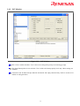
1
 8/16
IO Wizard V.1.31
Code Generator for R8C/ M16C/ H8
Microcomputer Development Environment System
Renesas Technology Singapore Pte. Ltd. 2009.05
www.renesas.com
IO Wizard User’s Manual – Code Generator for R8C/ M16C/ H8 Published by : Renesas Technology Singapore Pte. Ltd. Date : May 26th, 2009, V.1.31 Release 00 Copyright(C) Renesas Technology Singapore Pte. Ltd. All rights reserved. Trademarks a) General All brand or product names used in this manual are trademarks or registered trademarks of their respective companies or organizations. b) Specific Microsoft Windows is registered trademarks of Microsoft Corporation. IBM PC is a registered trademark of International Business Machines Corporation. Pentium is a registered trademark of Intel. InstallShield is a registered trademark and service mark of Macrovision Corporation and/or Macrovision Europe Ltd. 2
I C bus is a trademark of Koninklijke Philips Electronics N. V. IEBus is a trademark of NEC Electronics Corporation. i
IMPORTANT INFORMATION READ this user’s guide before using this software. KEEP the user’s guide handy for future reference. MCU: Throughout this document, the term “MCU” shall be defined as the Renesas R8C Tiny series microcomputers or Renesas M16C Tiny series. Improvement Policy: Renesas Technology Singapore Pte. Ltd. (hereafter collectively referred to as Renesas) pursues a policy of continuing improvement in design and performance of this software. Renesas reserves the right to change, wholly or partially, the specifications, design, user’s guide, and other documentation at any time without notice. Target User of the Product: This product should only be used by those who have carefully read and thoroughly understood the information as well as restrictions contained in the user’s guide. Do not attempt to use the product until you fully understand its mechanism. Support: This is a free of charge and ʺAS ISʺ basis software. We will not provide any support for this software. ii
LIMITED WARRANTY
Renesas warrants its products to be manufactured in accordance with published specifications and
free from defects in material and/or workmanship. The foregoing warranty does not cover damage
caused by fair wear and tear, abnormal store condition, incorrect use, accidental misuse, abuse,
neglect, corruption, misapplication, addition or modification or by the use with other hardware or
software, as the case may be, with which the product is incompatible. No warranty of fitness for a
particular purpose is offered. The user assumes the entire risk of using the product. Any liability of
Renesas is limited exclusively to the replacement of defective materials or workmanship.
DISCLAIMER
RENESAS MAKES NO WARRANTIES, EITHER EXPRESS OR IMPLIED, ORAL OR
WRITTEN, EXCEPT AS PROVIDED HEREIN, INCLUDING WITHOUT LIMITATION
THEREOF, WARRANTIES AS TO MARKETABILITY, MECRCHANTABILITY, FITNESS FOR
ANY PARTICULAR PURPOSE OR USE, OR AGAINST INFRINGEMENT OF ANY PATENT.
IN NO EVENT SHALL RENESAS BE LIABLE FOR ANY DIRECT, INCIDENTAL OR
CONSEQUENTIAL DAMAGES OF ANY NATURE, OR LOSSES OR EXPENSES RESULTING
FROM ANY DEFECTIVE PRODUCT, THE USE OF ANY PRODUCT OR ITS
DOCUMENTATION, EVEN IF ADVISED OF THE POSSIBILITY OF SUCH DAMAGES.
EXCEPT AS EXPRESSLY STATED OTHERWISE IN THIS WARRANTY, THIS PRODUCT IS
SOLD “AS IS”. AND YOU MUST ASSUME ALL RISK FOR THE USE AND RESULTS
OBTAINED FROM THE PRODUCT.
iii
All Right Reserved:
This user’s guide and product are copyrighted and all rights are reserved by Renesas. No part of this
user’s guide, all or part, any be reproduced or duplicated in any form, in hardcopy or machinereadable form, by any means available without Renesas‘s prior written consent.
Other Important Things to Keep in Mind:
1. Circuitry and other examples described herein are meant merely to indicate the characteristics
and performance of Renesas Technology‘s semiconductor products. Renesas assumes no
responsibility for any intellectual property claims or other problems that may result from
applications based on the examples described herein.
2. No license is granted by implication or otherwise under any patents or other rights of any third
party or Renesas.
3. MEDICAL APPLICATIONS: Renesas Technology’s products are not authorized for use in
MEDICAL APPLICATIONS without the written consent of the appropriate officer of Renesas
Technology (Asia Sales company). Such use includes, but is not limited to, use in life support
systems. Buyers of Renesas Technology’s products are requested to notify the relevant Renesas
Technology (Asia Sales offices) when planning to use the products in MEDICAL
APPLICATIONS.
Limited Anticipation of Danger:
Renesas cannot anticipate every possible circumstance that might involve a potential hazard. The
warnings in this user’s guide and on the product are therefore not all inclusive. Therefore, you must
use the product safely at your own risk.
iv
PREFACE About this manual
This user’s guide is written for Renesas IO Wizard software. It describes the operation and usage. Use
this guide to get started with using the IO Wizard.
The manual is organized as follows:
Section 1
About IO Wizard
Provides an overview to why the software is created
Section 2
Getting Started
Provides step-by-step guide to IO Wizard installation.
Section 3
Operation Guide
Presents IO Wizard GUI environment. Describes the different features and provides a
description on each specific window.
Section 4
Code Generation
Gives an overview on the generated files.
Section 5
Error Messages
Provides a description on the error report window and also offers advice to assist user to
input the correct setting.
An appendix containing links of relevant application notes and manuals are appended at the end of this
manual.
5
Article I.
Table of Contents
Article I. Table of Contents .....................................................................................................................6
Section 1. About IO Wizard......................................................................................................................8
Section 2. Getting Started .........................................................................................................................9
2.1
System Requirements...............................................................................................................9
2.2
Installation................................................................................................................................9
2.2.1
Installation Procedures .........................................................................................................9
2.2.2
Multiple Installation ...........................................................................................................13
2.2.3
Uninstall .............................................................................................................................13
2.2.4
IO Wizard folder ................................................................................................................13
Section 3. Operation Guide .....................................................................................................................14
3.1
Running IO Wizard ................................................................................................................14
3.2
Features of IO Wizard Window .............................................................................................15
3.2.1
GUI Environment...............................................................................................................15
3.2.2
Keyboard selection.............................................................................................................19
3.2.3
Link to HEW ......................................................................................................................20
3.2.4
Save and Load ....................................................................................................................23
3.3
Outline of R8C Tiny Series Window .....................................................................................25
3.3.1
System Setting Window .....................................................................................................25
3.3.2
Port Window ......................................................................................................................26
3.3.3
INT Window ......................................................................................................................27
3.3.4
Timer Window ...................................................................................................................28
3.3.5
Serial I/O Window .............................................................................................................30
3.3.6
CAN Window.....................................................................................................................32
3.3.7
ADC Window.....................................................................................................................33
3.3.8
DAC Window.....................................................................................................................34
3.3.9
Comparator Window ..........................................................................................................35
3.3.10 DTC Window .....................................................................................................................39
3.4
Outline of M16C Tiny Series Window ..................................................................................40
3.4.1
System Setting Window .....................................................................................................40
3.4.2
Port Window ......................................................................................................................41
3.4.3
INT Window ......................................................................................................................42
3.4.4
Timer Window ...................................................................................................................43
3.4.5
DMA Window....................................................................................................................45
3.4.6
UART Window ..................................................................................................................46
3.4.7
SI/O3 and SI/O4 Window ..................................................................................................48
3.4.8
Multi-master I2C Bus Window..........................................................................................49
3.4.9
CAN Window.....................................................................................................................50
3.4.10 ADC Window.....................................................................................................................51
3.5
Outline of H8 SLP Series Window ........................................................................................52
3.5.1
System Setting Window .....................................................................................................52
3.5.2
Port Window ......................................................................................................................53
3.5.3
IRQ Window ......................................................................................................................54
3.5.4
WKP Window ....................................................................................................................55
3.5.5
Timer Window ...................................................................................................................56
3.5.6
AEC Window .....................................................................................................................58
3.5.7
PWM Window ...................................................................................................................59
3.5.8
SCI1 Window.....................................................................................................................60
3.5.9
SCI31 and SCI32 Window.................................................................................................61
3.5.10 ADC Window.....................................................................................................................62
6
3.5.11 LCD Window .....................................................................................................................63
3.6
End Session ............................................................................................................................64
Section 4. Code Generation.....................................................................................................................65
4.1
Generated folder.....................................................................................................................65
4.2
Config.c, Config.h and Iodefine.h..........................................................................................66
Section 5. Error Messages.......................................................................................................................70
5.1
Error Report ...........................................................................................................................70
5.2
Error Message Table for R8C Tiny Series .............................................................................71
5.3
Error Message Table for M16C Tiny Series ..........................................................................85
5.4
Example of Computation Values for M16C Tiny Series .......................................................99
5.5
Error Message Table for H8 SLP Series ..............................................................................106
5.6
Example of Computation Values for H8 SLP Series ...........................................................111
Appendix A: Related Documents for R8C...............................................................................................119
Appendix B: Related Documents for M16C ............................................................................................122
Appendix C: Related Documents for H8/SLP for 38347 Group .............................................................123
Appendix D: Other Related Documents...................................................................................................124
7
Section 1. About IO Wizard
Renesas is aware that it is necessary for most first time users of our MCU to read the user’s manual,
application notes and technical news in order to proceed with software coding. One way to be familiar with any
MCU is to study the datasheet and the user manual intensively. This actually requires a period of time before the
user can embark on the software coding.
In the light of this learning process, IO Wizard, an easy-to-use GUI based standalone software, is
created specially to expedite the learning curve. User can generate start-up routines even with limited
knowledge of the Renesas MCU.
IO Wizard serves as a jumpstart for software engineer or student starting Renesas MCU based projects
helping them speeds up their software development process. Those interested to explore Renesas MCU will also
pick up knowledge of the MCU with much ease. Best of all, IO Wizard is available free for download from the
Renesas Web site.
We encourage user to read through this manual to understand the overall operation of IO Wizard before using
the software.
8
Section 2. Getting Started
2.1
System Requirements
IO Wizard requires the following system specification:
IBM PC/AT compatibles
Windows 2000
Windows XP
Windows Vista
Pentium II 233MHz or higher CPU is recommended.
128MB or more system memory is recommended.
Host Machine
OS
CPU
Memory
2.2
Installation
2.2.1 Installation Procedures
For installation, you will need to run the program IO WizardSetup.EXE. Double-click the IO
Wizard icon as shown in Figure 2-1.
Figure 2-1
IO Wizard Setup Icon
This will invoke IO Wizard Installer Welcome Screen as shown in Figure 2-2.
9
This runs the InstallShield Wizard and the following screen will be displayed.
Figure 2-2
IO Wizard Installer Welcome Screen
Click next to proceed with the installation.
Figure 2-3
License Agreement Screen
Choose “I accept the terms of the license agreement” and click next to proceed with the installation.
10
The following dialog box then allows you to select a directory in which to install IO Wizard:
Figure 2-4
Select Destination Directory Screen
Click OK to install into the default directory C:\Program Files\Renesas\IO Wizard , or specify an
alternative directory and click next.
Figure 2‐5 Ready to Install Screen Click install to begin the installation.
11
Figure 2‐6 Installing IO Wizard Screen The installer then copies the IO Wizard files to the specified directory.
Figure 2‐7 Installation Complete Screen Click on “Finish” to exit install program.
12
2.2.2 Multiple Installation
Figure 2‐8 Multiple Installation Screen IO WizardSetup allows installation of multiple copies of IO Wizard application. If a copy of IO
Wizard is already installed on user’s computer, a dialog will prompt user whether to continue
the new installation.
2.2.3 Uninstall
To uninstall, go to Start Menu -> Control Panel -> Add or Remove Programs.
2.2.4 IO Wizard folder
After installation, the following files/folders are present in IO Wizard folder.
1. IO Files Folder
2. Generated Folder
3. IO Wizard.exe
4. IO Wizard.ini
5. IO Wizard Read Me.txt
6. IO Wizard User’s Manual
7. IO Wizard FAQ
8. IO Wizard Quick Start Guide
13
Figure 2‐9 IO Wizard Folder Structure
Section 3. Operation Guide
3.1
Running IO Wizard
Double-click the IO Wizard icon as shown in Figure 3-1 found at:
C:\Program Files\Renesas\IO Wizard or go to Start Menu -> [Programs] -> [IO Wizard].
This will invoke IO Wizard Main window as shown in Figure 3-2.
IO Wizard.exe
Figure 3-1
IO Wizard Icon
14
3.2
Features of IO Wizard Window
3.2.1
GUI Environment
IO Wizard offers an easy-to-use dialog based software environment.
Select target mcu
Figure 3-2
Features of IO Wizard Main Window
Supported devices for R8C Tiny Series are R8C/10,R8C/11,R8C/12, R8C/13, R8C/1A, R8C/1B, R8C/22,
R8C/23, R8C/24, R8C/25, R8C/26, R8C/27, R8C/28, R8C/29, R8C/2A, R8C/2B, R8C/2C, R8C/2D,
R8C/2E, R8C/2F, R8C/2G, R8C/2H, R8C/2J, R8C/2K, R8C/2L, R8C/32A, R8C/33A and R8C/35A.
Supported devices for M16C Tiny Series are M16C/26A(48-pin device), M16C/28(80-pin device) and
M16C/29(80-pin device).
Supported device for H8 SLP Series is H8/38347(100-pin device).
When user selects a part no. from the combobox, the RAM and ROM size capacity of that part will be
reflected on display which is beside the pin configuration picture. Data flash size capacity will be
displayed when user selects a part no. from R8C/12, R8C/13, R8C/1B, R8C/23, R8C/25, R8C/27, R8C/29,
R8C/2B, R8C/2D, R8C/2F, R8C/2D, R8C/2F, R8C/2L, R8C/32A, R8C/33A, R8C/35A, M16C/26A,
M16C/28 or M16C/29.
User inputs the device selection, system setting and peripheral operation setting through IO setting area.
15
Figure 3-3
Next button (shown in Figure 3-2)
Click the <Next> button to proceed to the next window. Settings made in the window will be saved.
Peripheral Selection List
Combo Editbox
Combobox
Radiobutton
Tooltip
IO
Setting
Area
Peripheral
Tab Bar
Status List
Scrollbar
Clock Source Display
Figure 3-4
Features of IO Wizard Window
To select the specific peripheral dialog window to view, you can make the selection from the peripheral
selection list available on the left hand corner of the window (as shown in Figure 3-4) or click on the peripheral
tab to make a peripheral dialog window active.
The key features of IO Wizard window are described as follows:
Peripheral Selection List
: Gives you access to the individual peripheral window.
Peripheral tab bar
: Gives you access to the individual peripheral window conveniently by clicking on
the respective peripheral tab. Use the tab scrolling buttons to scroll through the
peripheral tabs.
: This sub-window displays the source code in real time according to selection
made through the IO setting area.
Status List
When user made an item selection at the IO setting area, that particular item will
be instantly highlighted in yellow in this window. The displayed code shown is
simultaneously updated according to current selection made by user.
16
Comments are display beside each line of code to aid user. Use the horizontal
scrollbar to browse through the source code displayed. If comment line is long,
user can use the horizontal scrollbar to view the complete comment.
: User inputs the device selection, system setting and peripheral operation setting
through this area
: When user places cursor at any of the setting area, short guide comments will be
displayed to help user in addition to the comment in the status list.
IO Setting area
Tooltip
Radiobutton
: Only one button can be selected at a time for a setting.
Checkbox
: Multiple buttons can be selected at a time.
Combobox
: Displays a dropdown list of selectable items.
Combo Editbox
: Displays a dropdown list of selectable items. It is also a single-line edit field that
allows user to enter a value for a setting.
Clock Source Display
: Displays the clock source selected in the main window.
When user selects a peripheral, which has interrupt setting, an interrupt setting window (as shown in Figure 3-5)
will slide out. User can make the interrupt selection in this window.
Interrupt Setting Window
Figure 3-5
Interrupt Setting Window for Interrupt Peripherals
17
Figure 3-6
Code highlighted in red
When user inputs an incorrect setting at combo editbox, source code shown on the status window will be
instantly highlighted in red. This error indicator draws user’s immediate attention to input the correct
setting.
[Note: The source code will also be highlighted in red, when user made a particular setting whereby the
calculated peripheral counter register value is out of range.]
Figure 3-7
Back button
User can click <Back> button to return to IO Wizard system setting main window to change CPU clock source.
But please take note of the below precaution before clicking the back button to amend the CPU clock source
setting.
Precaution:
All peripheral functions setting will be re-initialized to default whenever the CPU clock source is changed. This
is to ensure correct calculation is being carried out and right counter register values are set for peripheral
operations.
A warning dialog as shown in Figure 3-8 will appear when user clicks the <Back> button.
18
Figure 3-8
Warning Dialog
Figure 3-9
Generate button
After all settings are done, user can click <Generate> button to run code generation. User is still allow to amend
peripheral settings before clicking the button.
3.2.2
Keyboard selection
User can now use the keyboard to make the selection.
Press Ctrl key to move cursor into or out of IO Setting Area and interrupt setting window.
Press Tab key to move cursor to next control element.
Press Up and Down keys to change selection.
Press Space key to check a Checkbox.
When the <Generate> button is highlighted, user can press Space key to generate code.
19
3.2.3
Link to HEW
Figure 3-10
Generate dialog
After <Generate> botton is clicked, a “Generate” dialog as shown above, will pop out to prompt user to save the
generated files to their desired folder directory.
The generate dialog box now support 2 options for user to generate source files. They are “Output the source
files to specified folder” option and the “Link to HEW” option.
The Link to HEW option allows user to export the generated source codes into HEW. The prerequisite for this
option to work is that HEW 4.02 (or above) and HEW Target Server (COM) has already been installed.
Below are the steps required to install HEW Target Server and get it running:
1. You will need HEW 4.02(or above) installed on your machine.
If HEW is NOT installed on your machine:
Please contact a Renesas Sales Representative or Distributor and purchase an RSK (Renesas Starter Kit).
These kits come with all the development tools, and an AutoUpdate utility that will update the software
shipped with the tool to at least version 4.02
If HEW is already installed on your machine, please verify it is version 4.2 or above.
2. Preparing to use the HEW Target Server (COM)
Add HEWTargetServer.exe to your computers registry
Using Windows Explorer, surf to the directory where HEW was installed (in most cases, this is
C:\Program Files\Renesas\HEW\).
Double click on REGISTERSERVER.bat file
• HewTargetServer.exe will be registered in your computers registry.
• To remove HewTargetServer.exe from the registry, double-click on the
UNREGISTERSERVER.bat file located in the same folder.
Register the EcxHewTargetServer.dll within HEW
Launch High-performance Embedded Workshp
• From the Start Menu, click on All Programs -> Renesas -> High-Performance Embedded
Workshop -> High-performance Embedded Workshop
When the “Welcome” dialog box appears:
• Click the <Administration> button.
When the Tool Administration dialog box appears:
20
• Click on the <Register…> button
When the “Select HEW Registration File” Window appears, surf to: : the folder in which the Highperformance Embedded Workshop, or Renesas’s integrated development environment, is installed i.e.
C:\Program\Files\Renesas\HEW\System\SEC\HewTargetServer
• Double click on “EcxHewTargetServer.hrf”
Registration of EcxHewTargetServer.dll has completed.
NOTE: If EcxHewTargetServer.dll becomes unnecessary after you have registered it, use the Administration
Window to unregister it.
Linking to HEW
The Link to HEW option allows user to export the generated source codes into HEW only when HEW
workspace is opened. If HEW is not opened, IO Wizard will help user to invoke HEW.
When Link to HEW option is selected and OK is being clicked on the Generate dialog, a “HEW Project
Detected!” dialog as shown below, will pop out to inform user that the generated files will be inserted into HEW
workspace. If there are existing files in the workspace, the files will be overwritten.
Figure 3-11
HEW Project Detected! dialog
21
Figure below shows that the newly generated files are being inserted to an existing workspace.
Link to HEW feature
Generated Files inserted here
Figure 3-12
Inserting the generated files into HEW workspace
22
3.2.4 Save and Load
This feature allows user to save and load settings. User can perform save and load for settings made in the main
window, peripheral windows and interrupt setting windows.
Save Setting
Figure 3-13
Save button in Peripheral Setting Window
User can click <Save> button to save all current settings made. This includes those settings made in the Main
Window.
A “Save As” dialog as shown below, will pop out to prompt user to save their settings made into a file
(filename.iow) for loading in future sessions. The .iow file can be saved into user desired folder directory.
Figure 3-14
Save As dialog
23
Load Setting
Figure 3-15
Load button in Main Window
A “Load” button is added beside the “Next” button in the main window, it allows user to load any settings made
in settings made in prior sessions.
When user click the <Load> button, a “Open” dialog as shown below, will pop out to prompt user to open the
saved file. Once the selected “filename.iow” file is opened, all previous settings saved will be updated onto the
screen.
Figure 3-16
Open dialog
24
3.3
Outline of R8C Tiny Series Window
IO Wizard supports R8C Tiny Series system setting and a selection of peripherals available in
R8C/10,11,12,13,1A,1B,22,23,24,25,26,27,28,29,2A,2B,2C,2D,2E,2F,2G,2H,2J,2K,2L,32A,33A and 35A
which are Port 0 to Port 9, INT 0 to INT3, Key input interrupt, Timer X, Y, Z, C, RA, RB, RC, RD, RE, RF,
UART 0 to UART2, SSU, I2C, LIN, CAN ADC, DAC and Comparator. User is allowed to activate more than
one peripheral setting. Let’s look at each window in turn.
3.3.1 System Setting Window
Figure 3-18
System Setting in Main Window
IO Wizard supports CPU clock selection of on-chip oscillator, main clock, high-speed on chip oscillator
and sub-clock. Default CPU clock source is on-chip oscillator in Divide-by-8 mode.
For setting of main clock frequency, user is allowed to make their clock frequency selection from the
comobox dropdown list. For R8C/10 and R8C/12, the following clock frequencies are supported: 8MHz,
10MHz, 12MHz and 16MHz. For R8C/11, R8C/13, R8C/1A, R8C/1B, R8C/22, R8C/23, R8C/24,
R8C/25, R8C/26 R8C/27, R8C/28, R8C/29, R8C/2A, R8C/2B, R8C/2C, R8C/2D, R8C/2E, R8C/2F,
R8C/2K, R8C/2L, R8C/32A, R8C/33A and R8C/35A, the following clock frequencies are supported:
8MHz, 10MHz, 12MHz, 16MHz and 20MHz.
Clock frequency for on-chip oscillator is 125kHz. For R8C/11, 13, 1A, 1B, 2G, 2H and 2J, clock
frequency for high-speed on-chip oscillator is 8MHz. For R8C/22, 23, 24, 25, 26, 27, 28, 29, 2A, 2B, 2C,
2D, 2E, 2F, 2K and 2L, clock frequency for high-speed on-chip oscillator is 40MHz with frequency
division from 2 to 9.
25
For R8C/24, 25, 26, 27, 28, 29, 2A, 2B, 2C, 2D, 2G, 2H, 32A, 33A and 35A, sub-clock frequency is
32.768kHz.
Click the <Next> button to proceed to windows for peripheral function setting.
3.3.2 Port Window
Figure 3-19
Port Window
User is able to do settings for port directions and pull-ups.
Drive capacity setting is also available for Port 1(R8C/10,11,12,13,1A,1B,26,27,28,29,2E and 2F) or
Port 2(R8C/22,23,24,25,2A,2B,2C,2D,2K, 2L, 33A and 35A).
For Port 0, prc2 bit is set to 1 to enable write to PD0 register.
Port Input level select is supported in R8C/32A, 33A and 35A.
26
3.3.3 INT Window
Figure 3-20
INT Window
There are two different windows for INT0-INT3 setting and Key Input Interrupt setting.
User is able to do settings like priority level and input polarity.
For R8C/10,11,12,13,1A and 1B, tcc07 bit is set to 0 in INT3 interrupt.
Generated code includes interrupt function declaration and empty function body. Refer to section 4 for
details on code generation.
27
3.3.4 Timer Window
Figure 3-21
Timer Window
Each timer has its individual window for various setting like operation mode and count source.
User is allowed to de-activate or activate timer settings. All settings are disabled when [De-activate]
radiobutton is selected. To enable the settings, click on [Activate] radio button.
Following timers and operation modes are supported:
1) Timer X(R8C/10,11,12,13,1A and 1B):
- Timer mode
- Pulse output mode
- Event counter mode
- Pulse width measurement mode
- Pulse period measurement mode
2) Timer Y(R8C/10,11,12 and 13):
- Timer mode
- Programmable waveform generation mode
3) Timer Z(R8C/10,11,12,13,1A and 1B):
- Timer mode
- Programmable waveform generation mode
28
- Programmable one-shot generation mode
- Programmable wait one-shot generation mode
4) Timer C(R8C/10,11,12,13,1A and 1B):
- Input capture mode
- Output Compare mode
5) Timer RA(R8C/22,23,24,25,26,27,28,29,2A,2B,2C,2D,2E,2F,2G,2H,2J,2K,2L, 32A, 33A and 35A):
- Timer mode
- Pulse output mode
- Event counter mode
- Pulse width measurement mode
- Pulse period measurement mode
6) Timer RB(R8C/22,23,24,25,26,27,28,29,2A,2B,2C,2D,2E,2F,2G,2H,2J,2K,2L, 32A, 33A and 35A):
- Timer mode
- Programmable waveform generation mode
- Programmable one-shot generation mode
- Programmable wait one-shot generation mode
7) Timer RC(R8C/26,27,28,29,2A,2B,2C,2D,2E,2F,2K,2L, 32A, 33A and 35A):
- Input capture function (timer mode)
- Output compare function (timer mode)
- PWM mode
- PWM2 mode
8) Timer RD(R8C/22,23,24,25,2A,2B,2C,2D,2K,2L and 35A):
- Input capture function (timer mode)
- Output compare function (timer mode)
- PWM mode
- Reset synchronous PWM mode
- Complementary PWM mode
- PWM3 mode
9) Timer RE(R8C/22,23,24,25,26,27,28,29,2A,2B,2C,2D,2E,2F,2G, 2H, 32A, 33A and 35A):
- Real-time clock mode
- Output compare mode
10) Timer RF(R8C/2A,2B,2C,2D,2G,2H and 2J):
- Input capture mode
- Output compare mode
For each operation mode, the related function settings are supported while the unrelated setting are disabled.
User is allowed to enter timings and compare data in edit field or select them from combobox dropdown
list. Calculated value for register setting is being round to the nearest whole number.
29
3.3.5 Serial I/O Window
Figure 3-22
Serial I/O Window
Each serial I/O peripheral function has its individual setting window.
All settings are disabled by default when [Disabled] is selected from the first combobox.
Following serial I/O peripheral funcions and opertion modes are supported:
1) UART 0 and UART1:
- Clock Synchronous
a. Transmitter mode
b. Receiver mode
- UART (7 bits)
c. Transmitter mode
d. Receiver mode
- UART (8 bits)
e. Transmitter mode
f. Receiver mode
- UART (9 bits)
g. Transmitter mode
h. Receiver mode
30
UART 2 is supported for R8C/2A, 2B, 2C, 2D, 2G, 2H, 2K and 2L. It has the similar functions as UART 0
and UART 1.
UART 2 is also supported for R8C/32A, R8C/33A and R8C/35A. The UART 2 for these 3 devices has
similar functions as UART 2 in M16C/Tiny Series. It supports the following operating mode.
1) Clock synchronous
a. Transmitter mode
b. Receiver mode
2) UART (7 bits)
a. Transmitter mode
b. Receiver mode
3) UART (8 bits)
a. Transmitter mode
b. Receiver mode
4) UART (9 bits)
a. Transmitter mode
b. Receiver mode
5) I2C bus mode
a. Transmitter mode
b. Receiver mode
6) Special Mode 2
a. Transmitter mode
b. Receiver mode
7) IEBus mode
a. Transmitter mode
b. Receiver mode
8) SIM mode
a. Transmitter mode
b. Receiver mode
2) LIN(R8C/22,23,24,25,26,27,28,29,2A,2B,2C,2D,2E,2F,2G,2H,2J,2K, 2L, 32A, 33A and 35A):
- Slave mode
- Master mode
3) SSU(R8C/1A,1B,22,23,24,25,26,27,28,29,2A,2B,2C, 2D, 32A, 33A and 35A):
- Clock synchronous communication mode (SSU function)
a. Transmitter mode
b. Receiver mode
- Four-wire bus communication mode (SSU function)
c. Transmitter mode
d. Receiver mode
- I2C bus interface mode (I2C function)
b. Transmitter mode
c. Receiver mode
- Clock synchronous serial mode (I2C function)
a. Transmitter mode
b. Receiver mode
31
For each operation mode, the related function settings are supported while the unrelated setting are disabled.
User is allowed to enter transfer clock period and baud rate in edit field or select them from combobox
dropdown list. Calculated value for register setting is being round to the nearest whole number.
Precaution: Value set previously for Timer RA and UART0 will be overwritten when LIN is activated.
Count source for Timer RA is fixed to f1.
3.3.6 CAN Window
Figure 3-23
CAN Window
User is allowed to de-activate or activate CAN settings. All settings are disabled when [De-activate] radio
button is selected. To enable the settings, click on [Activate] radio button.
User is able to do settings like fCAN clock, sampling control and message order.
32
3.3.7 ADC Window
Figure 3-24
ADC Window
User is allowed to de-activate or activate ADC settings. All settings are disabled when [De-activate] radio
button is selected. To enable the settings, click on [Activate] radio button.
User is able to do settings like selecting analog input pin, operating mode and resolution.
33
3.3.8 DAC Window
Figure 3-25
DAC Window
User is allowed to de-activate or activate DAC settings. All settings are disabled when [De-activate] radio
button is selected. To enable the settings, click on [Activate] radio button.
User is able to do settings like entering DAC output value.
34
3.3.9 Comparator Window
Figure 3-26
Comparator Window for R8C/2E and 2F
User is allowed to de-activate or activate Comparator settings. All settings are disabled when
[De-activate] radio button is selected. To enable the settings, click on [Activate] radio button.
Settings are available for Comparator 0 and Comparator 1.
35
Figure 3-27
Comparator Window for R8C/2G, 2H and 2J
User is allowed to de-activate or activate Comparator settings. All settings are disabled when
[De-activate] radio button is selected. To enable the settings, click on [Activate] radio button.
Settings are available for Comparator 1 and Comparator 2.
36
Figure 3-28
Comparator A Window for R8C/32A, 33A and 35A
User is allowed to de-activate or activate Comparator A settings. All settings are disabled when
[De-activate] radio button is selected. To enable the settings, click on [Activate] radio button.
Settings are available for Comparator A1 and Comparator A2.
37
Figure 3-29
Comparator B Window for R8C/32A, 33A and 35A
User is allowed to de-activate or activate Comparator B settings. All settings are disabled when
[De-activate] radio button is selected. To enable the settings, click on [Activate] radio button.
User can make the related interrupt settings through INT 0 – INT 3 windows.
38
3.3.10 DTC Window
Figure 3-30
DTC Window for R8C/32A, 33A and 35A
User is allowed to de-activate or activate DTC settings. All settings are disabled when
[De-activate] radio button is selected. To enable the settings, click on [Activate] radio button.
User is able to select [Ctrl Data Allocation] (dtcd0~dtcd23, 24 blocks) and then tick on the
[Enable] checkbox to configure the settings. All the code settings will be prefixed with “dtcdi_”
(i = 0~23).
User is able to select [DTC Activation Enable] (dtcen0~dtcen6, 7 registers) and then tick on the
[Enable] checkbox to show different register bits for subsequent configuration of settings.
39
3.4
Outline of M16C Tiny Series Window IO Wizard supports M16C/Tiny Series system settings and a selection of peripherals available in M16C/26A, 28
and 29 which are Port 0 to Port 3, Port 6 to Port 10, INT 0 to INT 5, Key Input Interrupt, Timer A0 to Timer A4,
Timer B0 to Timer B2, Three-phase Motor Control Timer, Timer S, DMA0, DMA1, UART0 to UART2, SI/O3,
SI/O4, Multi-master I2C Bus, CAN and ADC. User is allowed to activate more than one peripheral setting.
Let’s look at each window in turn.
3.4.1
System Setting Window
Figure 3-31
M16C/Tiny Series System Setting in Main Window
IO Wizard M16C/Tiny Series supports CPU clock selection of on-chip oscillator, main clock, sub-clock
and PLL clock. Default CPU clock source is on-chip oscillator in Divide-by-8 mode.
The on-chip oscillator source by default is using frequency source f2(ROC)-2MHz in Divide-by-2
mode. On-chip oscillator frequency source supported are: f1(ROC) – 1MHz, f2(ROC) – 2MHz and
f3(ROC) – 16MHz. CPU clock source in on-chip oscillator is on-chip oscillator frequency source
selected divided by on-chip oscillator division selected. For example: frequency source 2MHz selected
and on-chip oscillator divide-by-2 mode selected. CPU clock freqeuncy will be 2MHz divide by 2,
which is 1MHz.
For setting of main clock frequency, user is allowed to make their clock frequency selection from the
40
combobox dropdown list. Clock frequencies supported are: 5MHz, 8MHz, 10MHz, 12MHz, 16MHz
and 20MHz.
For setting of PLL clock frequency, user is allowed to multiply the main clock frequency selection from
the combobox dropdown list with PLL multiplying factor combobox dropdown list. For example, main
clock frequency 5MHz selected and PLL multiplying factor selected is multiply by 4. The result of CPU
clock frequency will be 5MHz multiply by 4, which is 20MHz. Note: user is only allowed to set the
clock frequency between 10MHz and 20MHz.
Clock frequency for sub-clock is 32768Hz.
Click the <Next> button to proceed to Port 0 window.
3.4.2
Port Window
Figure 3-32
Port Window
Ports have similar windows.
User is able to do settings for port directions and pull-up.
Drive capacity setting is disabled here as it is not applicable.
For Port 9, prc2 bit is set to 1 to enable write to PD9 register.
41
3.4.3
INT Window
Figure 3-33
INT Window
INT 0-5 have similar windows. User is able to do settings like priority level and trigger edge.
Key Input Interrupt has its own window. User is able to do interupt piority level only. Other settings are
disabled.
Generated code include interrupt function declaration and empty function body. Refer to section 4 for
details on code generation.
42
3.4.4
Timer Window
Figure 3-34
Timer Window
Each timer has its individual window. In these timers, Timer A0 – Timer A4 have similar windows and
Timer B0 – Timer B2 have similar windows.
User is allowed to de-activate or activate Timer settings. All settings are disabled when [De-activate]
radiobutton is selected. To enable the settings, click on [Activate] radio button.
The following timers and operation modes are supported:
1) Timer A0 – Timer A4:
- Timer mode
- Event counter mode
- One-shot timer mode
- PWM mode
2) Timer B0 – Timer B2
- Timer mode
- Pulse period measure mode
- Pulse width measure mode
- Event counter mode
- A/D trigger mode (available for Timer B0 and Timer B1 only)
43
3) Three Phase Motor Control Timer
4) Timer S(M16C/28 and M16C/29):
- Waveform generation mode
- Timer measurement mode
For each operation mode, the related function settings are supported while the unrelated setting are disabled.
For Timer A0 – A4 and Timer B0 – B2, user is allowed to enter count value in edit field or select
selected timings available from the combobox dropdown list. Calculated value for register setting is
being round to the nearest whole number.
For Three-phase Motor Control Timer, fixed timings are supported in Carrier Wave Cycle, Dead Time
and PWM 50% Duty Cycle with fixed clock source f1. User is allowed to select selected timings
available from the combobox dropdown list. Calculated value is being round to the nearest whole
number.
Precaution: Settings in three-phase motor control timer will overwrite the settings made in Timer A1,
A2, A4 and B4 in the generated output file.
For Timer S, fixed timings are supported in Default Output Level and SR Waveform Level (Set Width
and Reset Width). User is allowed to select selected timings available from the combobox dropdown
list. Calculated value is being round to the nearest whole number and is based on free-running operation
mode.
44
3.4.5
DMA Window
Figure 3-35
DMA Window
DMA0 and DMA1 have similar window. The discussion below referring to DMA0 is also applicable to
DMA1.
User is allowed to de-activate or activate DMA0 settings. All settings are disabled when [De-activate]
radiobutton is selected. To enable the settings, click on [Activate] radio button.
User is able to do settings like Transfer Bit, Transfer Mode, DMA Request Cause and Source to
Destination Direction.
User is allowed to input address pointer for source address and destination address and transfer count.
45
3.4.6
UART Window
Figure 3-36
UART Window
UART 0 and UART 1 have similar window. The discussion below referring UART 0 is also applicable
to UART 1. UART 2 has its own window, and the operation modes are different from UART 0 and
UART 1.
All settings are disabled by default when [Disabled] is selected from Serial Interface Mode combobox.
UART 0 and UART 1 support the following serial interface operating modes.
1) Clock Synchronous
a. Transmitter mode
b. Receiver mode
2) UART (7 bits)
a. Transmitter mode
b. Receiver mode
3) UART (8 bits)
a. Transmitter mode
b. Receiver mode
4) UART (9 bits)
a. Transmitter mode
b. Receiver mode
UART 2 supports the following operating mode.
7) Clock synchronous
c. Transmitter mode
46
d. Receiver mode
8) UART (7 bits)
a. Transmitter mode
b. Receiver mode
9) UART (8 bits)
a. Transmitter mode
b. Receiver mode
10) UART (9 bits)
a. Transmitter mode
b. Receiver mode
11) I2C bus mode
c. Transmitter mode
d. Receiver mode
12) Special Mode 2
c. Transmitter mode
d. Receiver mode
9) IEBus mode
c. Transmitter mode
d. Receiver mode
10) SIM mode
c. Transmitter mode
d. Receiver mode
For each operation mode, the related function settings are supported while the unrelated setting are disabled.
Calculated value for register setting is being round to the nearest whole number. For example if u0brg is
calculated to be 11.5, u0brg value is being round up to 12. If u0brg is calculated to be 11.4, u0brg value
is being round down to 11.
47
3.4.7
SI/O3 and SI/O4 Window
Figure 3-37
SI/O3 Window
SI/O3 and SI/O4 window is available in M16C/28 and M16C/29 only.
SI/O3 and SI/O4 have similar window. The discussion below referring to SI/O3 is also applicable to
SI/O4.
User is allowed to de-activate or activate SI/O3 settings. All settings are disabled when [De-activate]
radiobutton is selected. To enable the settings, click on [Activate] radio button.
User is able to do settings like Clock Select, Internal Clock Source, Sout Output Enable, Transfer
Direction and Clock Polarity.
User is allowed to input value for transfer clock period and transmit data.
Calculated value for transfer clock period is being round to the nearest whole number. For example if
s3brg is calculated to be 11.5, s3brg value is being round up to 12. If s3brg is calculated to be 11.4,
s3brg value is being round down to 11.
48
3.4.8
Multi-master I2C Bus Window
Figure 3-38
Multi-master I2C Bus Window
Multi-master I2C bus window is available in M16C/28 and M16C/29 only.
User is allowed to de-activate or activate Multi-master I2C bus settings. All settings are disabled when
[De-activate] radiobutton is selected. To enable the settings, click on [Activate] radio button.
User is able to do settings like Clock Select, I2C System Clock, SCL Mode and ACK Clock.
User is allowed to input value for SCL Frequency Control and SCL Release Time.
Calculated value for SCL Frequency Control and SCL Release Timer will be shown in the comment
under the status list.
49
3.4.9
CAN Window
Figure 3-39
CAN Window
CAN window is available in M16C/29 only.
User is allowed to de-activate or activate CAN settings. All settings are disabled when [De-activate]
radiobutton is selected. To enable the settings, click on [Activate] radio button.
User is able to do settings like enabling Listen-only Mode, Basic CAN, Loop Back Mode Enable etc.
50
3.4.10 ADC Window
Figure 3-40
ADC Window
User is allowed to de-activate or activate ADC settings. All settings are disabled when [De-activate]
radio button is selected. To enable the settings, click on [Activate] radio button.
User is able to do settings like selecting A/D input group, analog input pin, operating mode and
resolution.
ADC supports 8 different types of operating mode:
1)
2)
3)
4)
5)
6)
7)
8)
One-shot mode
Repeat mode
Single sweep mode
Repeat sweep mode 0
Repeat sweep mode 1
Simultaneous sample sweep mode
Delayed trigger mode 0
Delayed trigger mode 1
For each operation mode, the related function settings are supported while the unrelated setting are disabled.
51
3.5
Outline of H8 SLP Series Window
IO Wizard supports H8/SLP Series system settings and a selection of peripherals available in H8/38347 which
are Port 1 to Port 9, Port A, IRQ0 to IRQ4, WKP0 to WKP7, Timer A, Timer C, Timer F, Timer G, AEC, PWM,
SCI1, SCI31, SCI32, ADC and LCD. User is allowed to use more than one peripheral setting. But, input-ports
only which are Port C and Port D are not available. Let’s look at each window in turn.
3.5.1 System Setting Window
Figure 3-41
H8/SLP Series System Setting in Main Window
IO Wizard H8/SLP Series supports Operation Mode with Active High Speed Mode only. Default of
Sub-clock Oscillator Pin is From X1.
For setting of System clock frequency as CPU operating clock, user is allowed to make their clock
frequency selection from the combobox dropdown list. Clock frequencies supported are: 2MHz, 5MHz,
8MHz..
For setting of Frequency Value for Sub-clock, user is allowed to to make their clock frequency selection
from the combobox dropdown list. Clock frequencies supported are: 32.768KHz and 38.4KHz.
Click the <Next> button to proceed to the Port 1 window.
52
3.5.2 Port Window
Figure 3-42
Port Window
Ports have similar windows.
User is able to do settings for Pin Status.
For Port 1, 3, 5 and 6, user is also able to do settings for MOS Input Pull Up.
For Port 2, user is also able to do settings for Data Output.
53
3.5.3 IRQ Window
Figure 3-43
IRQ Window
User is able to do settings for Interrupt Enable and Active edge.
54
3.5.4 WKP Window
Figure 3-44
WKP Window
User is able to do settings like Interrupt Enable and trigger edge.
Generate interrupt function declaration and empty function body. Refer to section 4 for details on code
generation.
55
3.5.5 Timer Window
Figure 3-45
Timer Window
Each timer has its individual window for various setting like operation mode and count source.
User is allowed to choose to use Timer settings. All settings are disabled when [No] radiobutton is
selected. To enable the settings, click on [Yes] radio button.
The following timers and operation modes are supported:
1) Timer A supports 4 different operating modes.
- Interval Timer mode
- Real Time Clock mode
- System Clock output mode
- Subclock output mode
For each operation mode, the related function settings are supported while the unrelated setting are disabled.
Additional information is provided for Interval Timer mode. Overflow times is calculated and displayed on
the comment. Calculated value is being round to the nearest number with accuracy ±0.01ms.
Additional information is provided for System Clock output. Clock cycle is calculated and displayed on the comment. Calculated value is being round to the nearest number with accuracy ±0.1us.
56
Additional information is provided for Subclock output. Clock cycle is calculated and displayed on the comment. Calculated value is being round to the nearest number with accuracy ±1us.
2) Timer C supports 3 different operating modes.
- Interval Timer mode
- Timer (auto-reload) mode
- Event Counter
For each operation mode, the related function settings are supported while the unrelated setting are disabled.
Fixed timings are supported for Interval timer mode and Timer (auto-reload) mode. User is allowed to select
selected timings available from the combobox dropdown list. Calculated value is being round to the nearest
whole number.
3) Timer F supports 5 operating modes.
- Timer (8 bits) mode
- Timer (16 bits) mode
- Output Compare Match (8 bits) mode
- Output Compare Match (16 bits) mode
- Event Counter mode
For each operation mode, the related function settings are supported while the unrelated setting are disabled.
Fixed timings are supported for Timer (8 bits) mode, Timer (16 bits) mode, Output Compare Match (8 bits)
mode and Output Compare Match (16 bits) mode. User is allowed to select selected timings available from
the combobox dropdown list. Calculated value is being round to the nearest whole number.
4) Timer G supports 2 operating modes.
- Interval Timer mode
- Input Capture mode
For each operation mode, the related function settings are supported while the unrelated setting are disabled.
57
3.5.6 AEC Window
Figure 3-46
AEC Window
User is allowed to choose to use AEC settings. All settings are disabled when [No] radiobutton is
selected. To enable the settings, click on [Yes] radio button.
AEC supports 2 types of Channel Select.
1) 16 bit event counter
2) 8 bit event counter
For each operation mode, the related function settings are supported while the unrelated setting are disabled.
User is able to do settings like Count Up Enable H and Count Up Enable L in 8-bit event counter of
Channel Select.
58
3.5.7 PWM Window
Figure 3-47
PWM Window
User is allowed to choose to use PWM settings. All settings are disabled when [No] radiobutton is
selected. To enable the settings, click on [Yes] radio button.
Fixed Duty Cycle is supported for 14-bit PWM mode. User is allowed to select Duty Cycle available
from the combobox dropdown list. Calculated value is being round to the nearest whole number.
59
3.5.8 SCI1 Window
Figure 3-48
SCI1 Window
User is allowed to choose to use SCI1 settings. All settings are disabled when [No] radiobutton is
selected. To enable the settings, click on [Yes] radio button.
1)
2)
3)
4)
5)
SCI1 supports 5 operating modes.
Synchronous (8 bit) mode
Synchronous (16 bit) mode
Synchronized Serial Bus (8 bit) mode
Synchronized Serial Bus (16 bit) mode
Continuous clock output
For each operation mode, the related function settings are supported while the unrelated setting are disabled.
Additional information is provided for 5 operating modes. Serial Clock Cycle is calculated and displayed
on the comment. Calculated value is being round to the nearest number with accuracy ±0.1us.
60
3.5.9 SCI31 and SCI32 Window
Figure 3-49
SCI31 Window
SCI31 and SCI32 have similar window. The discussion below referring to SCI31 is also applicable to
SCI32.
All settings are disabled by default when [Disabled] is selected from Communication Mode combobox.
SCI31 supports the following serial interface operating modes.
1) Synchronous
a. Transmitter mode
b. Receiver mode
2) Asynchronous (5 bits)
a. Transmitter mode
b. Receiver mode
3) Asynchronous (7 bits)
a. Transmitter mode
b. Receiver mode
4) Asynchronous (8 bits)
a. Transmitter mode
b. Receiver mode
For each operation mode, the related function settings are supported while the unrelated setting are disabled.
61
Calculated value for SCI31.BRR is being round to the nearest whole number. For example if
SCI31.BRR is calculated to be 11.5, SCI31.BRR value is being round up to 12. If SCI31.BRR is
calculated to be 11.4, SCI31.BRR value is being round down to 11.
3.5.10 ADC Window
Figure 3-50
ADC Window
User is allowed to choose to use ADC settings. All settings are disabled when [No] radiobutton is
selected. To enable the settings, click on [Yes] radio button.
User is able to do settings like selecting A/D Conversion Speed, Analog Input Pin and External Trigger.
Additional information is provided for A/D Conversion Speed. Conversion times is calculated and
displayed on comment. Calculated value is being round to the nearest number with accuracy ±0.1us. If
the Conversion times faster than the minimum conversion times, warning message is displayed. Do not
ignore the warning message. User should use the conversion times that in the supported range in order
to get accurate ADC value.
62
3.5.11 LCD Window
Figure 3-51
LCD Window
User is allowed to choose to use LCD settings. All settings are disabled when [No] radiobutton is
selected. To enable the settings, click on [Yes] radio button.
User is able to do settings like selecting LCD Drive Power, Display Function, Display Data Control,
Drive Waveform, Duty Selection/Common Function, Segment Driver, Frame Frequency Select and
Charge/discharge Pulse Cycle Duty.
63
3.6
End Session
To end the IO Wizard Window:
Close the window by clicking
in the upper-right corner of the window.
Close IO Wizard taskbar button as shown in Figure 3-52. Right-click the taskbar button and then click
Close.
Figure 3-52
Close IO Wizard by clicking taskbar button
64
Section 4. Code Generation
4.1
Generated folder
After all settings are done, user can click generate button to run code generation. With that if all settings made
are valid, 3 files (one .c file and two .h files) will be generated and are stored to the Generated folder. Otherwise,
error report window appears and display error messages if incorrect setting is made. No files will be generated
when there is error. Refer to section 5 error messages for details.
The following files are present in the Generated folder:
a. Config.c
Source file.
Includes system initialization (e.g. system clock setting), peripheral setting routines and empty
function body.
b. Config.h
Header file. Includes global function declaration and interrupt function declaration.
c. sfr_R8C10config.h/sfr_R8C11config.h/sfr_R8C12config.h/sfr_R8C13config.h/sfr_R8C
1Aconfig.h/sfr_R8C1Bconfig.h/sfr_R8C22config.h/sfr_R8C23config.h/sfr_R8C24confi
g.h/sfr_R8C25config.h/sfr_R8C26config.h/srf_R8C27config.h/sfr_R8C28config.h/sfr_
R8C29config.h/sfr_R8C2Aconfig.h/sfr_R8C2Bconfig.h/sfr_R8C2Cconfig.h/sfr_R8C2
Dconfig.h/ sfr_R8C2Econfig.h/ sfr_R8C2Fconfig.h/ sfr_R8C2Gconfig.h/
sfr_R8C2Hconfig.h/ sfr_R8C2Jconfig.h/ sfr_R8C2Kconfig.h/
sfr_R8C2Lconfig.h/sfr_R8C32Aconfig.h/sfr_R8C33Aconfig.h/sfr_R8C35Aconfig.h/sfr
_M16C26Aconfig.h/sfr_M16C28config.h/sfr_M16C29config.h
(Note: File to be generated will depend on the MCU selected.)
Header file for SFRs declaration. Declares the system settings and specific
SFRs definitions like defining individual bit of any specific SFR register.
For H8/SLP Series, the following files are also generated and present in the Generated folder:
d. Intprg.c
Source file for interrupt functions.
e. Io.define.h
Header file for definition of I/O Register for H8/38347 Group.
65
Figure 4-1
Folder Structure of Generated Folder
The output files have to go through code compilation process before user can obtain the object file. The files
does not include any startup program hence it is a free project. User may use Renesas M3T-NC8C C compiler
for R8C Tiny Series or Renesas M3T-NC30WA to compile the program code. Contact your nearest Renesas
sales offices to request for this free version software.
4.2
Config.c, Config.h and Iodefine.h
Figure 4-2 to figure 4-5 are screenshots of Config.c. Under each peripheral heading, there are useful additional
guidelines to inform user to perform correct settings. For example, refer to Figure 4.5, AN3 is selected in ADC
analog input pin setting and there is a comment “Set AN3 pin to input direction” to remind user. Figure 4-6 is a
screenshot of Config.h. Figure 4-7 is a screenshot of Iodefine.h.
66
Figure 4‐2 Sample output of Config.c (1)
Figure 4-3
Sample output of Config.c (2) 67
Figure 4-4
Sample output of Config.c (3)
Figure 4-5
Sample output of Config.c (4) 68
Figure 4-6
Figure 4-7
Sample output of Config.h Sample output of iodefine.h
69
Section 5. Error Messages
5.1
Error Report
The Error Report window provides a form of look up table for user to identify the error occurred. It reflects
exactly which setting box is incorrectly set.
An error number is being assigned to each error message and brief help is provided to assist user to input the
correct setting.
Figure 5‐1 Error Report Window
70
5.2
Error Message Table for R8C Tiny Series
When an error occurs, user should look up the error code number and error description listed in the error
report window from the Error Message table below. When in doubt, refer to the table below for additional
notes and advice to input the correct setting.
No.
Error Message
01 Invalid value entered at Timer X – Timer
Value
Notes and Action
Enter only 0.5ms, 1ms, 2ms or 4ms only.
CPU Clock:
On-chip oscillator
125kHz
Main clock
16MHz
Internal Count Source:
No division
Divide by 2
Divide by 8
Divide by 32
Formula:
Timer Value entered = [(PREX+1) x (TX+1)] x (Internal Count Source /System
Clock)
Example to calculate value of PREX and value of TX:
Desired timer value entered = 1ms
Based on the formula above, if main clock is chosen and Internal clock source is
divide by 2:
Timer Value entered = [(PREX+1) x (TX+1)] x (Internal Count Source /System
Clock)
1ms = [(PREX+1) x (TX+1)] x (2/16MHz)
1ms = [(PREX+1) x (TX+1)] x 125ns
[(PREX+1) x (TX+1)] = 1ms/125ns
[(PREX+1) x (TX+1)] = 8000
Through calculation: 250 x 32 = 8000
Note: PREX valid range: 0~255 and TX valid range: 0~255
PREX+1 =250 and TX+1 = 32
Hence, PREX =250 -1 which is 249 and TX = 32 -1 which is 31
02 Invalid value entered at Timer X – PREX Enter value for PREX. PREX valid range: 0~255.
03 Invalid value entered at Timer X – TX
Enter value for TX. TX valid range: 0~255.
04 Value entered exceeded maximum value Maximum acceptable value is 255. PREX valid range: 0~255.
at Timer X - PREX
05 Value entered exceeded maximum value Maximum acceptable value is 255. TX valid range: 0~255.
at Timer X – TX
06 Invalid value entered at Timer Y – Timer
Value
Enter only 0.5ms, 1ms, 2ms or 4ms only.
Formula:
Timer value entered =[(PREY+1) x (TYPR+1)] x (Internal Count Source /System
Clock)
Refer to no. 1 example calculation. Similar as Timer X – Timer Value.
71
07 Invalid value entered at Timer Y – Primary CPU Clock:
Period
On-chip oscillator
125kHz
Main clock
16MHz
Internal Count Source:
No division
Divide by 8
fRING
Formula:
Timer Value entered = [(PREY+1) x (TYPR+1)] x (Internal Count Source /System
Clock)
In this case, PREY is fixed at 249 (actual count is 250).
Example to calculate value of TYPR:
Desired timer value entered = 10ms
Based on the formula above, if main clock is chosen and Internal clock source is
divide by 8:
Note: TYPR valid range is 0~255.
Timer Value entered = [(PREY+1) x (TYPR+1)] x (Internal Count Source /System
Clock)
10ms = [(249 +1) x (TYPR+1)] x (8/16MHz)
10ms = [ 250 x (TYPR+1)]/0.5us
250 x (TYPR+1) = 10ms/0.5us
250 x (TYPR+1) = 20000
TYPR+1 = 20000/250
TYPR = 80 -1
Therefore, TYPR = 79
08 Invalid value entered at Timer Y –
Secondary Period
Formula:
Timer Value entered = [(PREY+1) x (TYSC+1)] x (Internal Count Source / System
Clock)
In this case, PREY is fixed at 249 (250 - 1).
Refer to no. 7 example calculation. Similar as Timer Y – Primary Period.
09 Value entered is below minimum value at Formula:
Timer Y - Primary Period
Timer Value entered = [(PREY+1) x (TYPR+1)] x (Internal Count Source /System
Clock)
PREY is fixed at 249 (actual count is 250).
10 Value entered is below minimum value at Formula:
Timer Y - Secondary Period
Timer Value entered = [(PREY+1) x (TYSC+1)] x (Internal Count Source /System
Clock)
PREY is fixed at 249 (actual count is 250).
11 Value entered exceeded maximum value Formula:
at Timer Y – Primary Period
Timer Value entered = [(PREY+1) x (TYPR+1)] x (Internal Count Source /System
Clock)
PREY is fixed at 249 (actual count is 250).
12 Value entered exceeded maximum value Formula:
at Timer Y – Secondary Period
Timer Value entered = [(PREY+1) x (TYSC+1)] x (Internal Count Source /System
Clock)
PREY is fixed at 249 (actual count is 250).
72
13 Invalid value entered at Timer Z – Timer
Value
Enter only 0.5ms, 1ms, 2ms or 4ms only.
Formula:
Timer value entered =[(PREZ+1) x (TZPR+1)] x (Internal Count Source /System
Clock)
Refer to no. 1 for example calculation. Similar as Timer X – Timer Value.
14 Invalid value entered at Timer Z – Primary Formula:
Period
Timer Value entered = [(PREZ+1) x (TZPR+1)] x (Internal Count Source /System
Clock)
In this case, PREZ is fixed at 249 (actual count is 250).
Refer to no. 7 for example calculation. Similar as Timer Y – Primary Period.
15 Invalid value entered at Timer Z –
Secondary Period
Formula:
Timer Value entered = [(PREZ+1) x (TZSC+1)] x (Internal Count Source / System
Clock)
In this case, PREZ is fixed at 249 (250 - 1).
Refer to no. 7 for example calculation. Similar as Timer Y – Primary Period.
16 Invalid value entered at Timer Z – Wait
time
Formula:
Timer Value entered = [(PREZ+1) x (TZPR+1)] x (Internal Count Source /System
Clock)
In this case, PREZ is fixed at 249 (actual count is 250).
Refer to no. 7 example calculation. Similar as Timer Y – Primary Period.
17 Invalid value entered at Timer Z – OneShot Pulse Output time
Formula:
Timer Value entered = [(PREZ+1) x (TZSC+1)] x (Internal Count Source / System
Clock)
In this case, PREZ is fixed at 249 (250 - 1).
Refer to no. 7 example calculation. Similar as Timer Y – Primary Period.
18 Value entered is below minimum value at Formula:
Timer Z - Primary Period
Timer Value entered = [(PREZ+1) x (TZPR+1)] x (Internal Count Source /System
Clock)
PREZ is fixed at 249 (actual count is 250).
19 Value entered is below minimum value at Formula:
Timer Z - Secondary Period
Timer Value entered = [(PREZ+1) x (TZSC+1)] x (Internal Count Source /System
Clock)
PREZ is fixed at 249 (actual count is 250).
20 Value entered is below minimum value at Formula:
Timer Z - Wait Time
Timer Value entered = [(PREZ+1) x (TZPR+1)] x (Internal Count Source /System
Clock)
PREZ is fixed at 249 (actual count is 250).
21 Value entered is below minimum value at Formula:
Timer Z - One-Shot Pulse Output Time
Timer Value entered = [(PREZ+1) x (TZSC+1)] x (Internal Count Source /System
Clock)
PREZ is fixed at 249 (actual count is 250).
73
22 Value entered exceeded maximum value Formula:
at Timer Z – Primary Period
Timer Value entered = [(PREZ+1) x (TZPR+1)] x (Internal Count Source /System
Clock)
PREZ is fixed at 249 (actual count is 250).
23 Value entered exceeded maximum value Formula:
at Timer Z – Secondary Period
Timer Value entered = [(PREZ+1) x (TZSC+1)] x (Internal Count Source /System
Clock)
PREZ is fixed at 249 (actual count is 250).
24 Value entered exceeded maximum value Formula:
at Timer Z – Wait Time
Timer Value entered = [(PREZ+1) x (TZPR+1)] x (Internal Count Source /System
Clock)
PREZ is fixed at 249 (actual count is 250).
25 Value entered exceeded maximum value Formula:
at Timer Z – One-Shot Pulse Output Time Timer Value entered = [(PREZ+1) x (TZSC+1)] x (Internal Count Source /System
Clock)
PREZ is fixed at 249 (actual count is 250).
26 Invalid value entered at UART 0 - Transfer CPU Clock:
Clock Period
On-chip oscillator
125kHz
Main clock
16MHz
BRG Clock Select:
No division
Divide by 8
Divide by 32
Formula:
u0brg+1 = [(System Clock/BRG Clock Select ) x Transfer Clock period entered ] / 2
Example to calculate value of u0brg:
Desired baud rate entered = 200us
Based on the formula above, if on-chip oscillator is chosen and BRG clock select is
no division:
Note: u0brg valid range is 0~255.
u0brg+1 = [(System Clock/BRG Clock Select ) x Transfer Clock period entered ] / 2
u0brg+1 = [(125KHz/1 )x 200] / 2
u0brg+1 = 25 / 2
u0brg+1 = 12.5
u0brg = 12.5 - 1
u0brg = 11.5
u0brg = 12 (Round down to nearest whole number)
74
27 Invalid value entered at UART 0 - Baud
Rate
CPU Clock:
On-chip oscillator
125kHz
Main clock
16MHz
BRG Clock Select:
No division
Divide by 8
Divide by 32
Formula:
u0brg+1 = (System Clock/BRG Clock Select ) / (Baud Rate entered x 16)
Example to calculate value of u0brg:
Desired baud rate entered = 9600 bps
Based on the formula above, if main clock is chosen and BRG clock select is no
division:
Note: u0brg valid range is 0~255.
u0brg+1 = (System Clock/BRG Clock Select ) / (Baud Rate entered x 16)
u0brg+1 = (16MHz/1 ) / (9600 x 16)
u0brg+1 = 16MHz / 153600
u0brg+1 = 104.166
u0brg = 104.166 - 1
u0brg = 103.166
u0brg = 103 (Round down to nearest whole number)
28 Invalid value entered at UART 0 Transmit Data
Enter 7-9 bits transmission data.
Example: 1111000 is 7 bits, 01001111 is 8 bits and 100001111 is 9 bits.
29 Value entered is below minimum value at Formula:
UART 0 - Transfer Clock Period
u0brg+1 = [(System Clock/BRG Clock Select ) x Transfer Clock period entered ] / 2
Refer to no. 26 example calculation.
30 Value entered is below minimum value at Formula:
UART 0 - Baud Rate
u0brg+1 = (System Clock/BRG Clock Select ) / (Baud Rate entered x 16)
31 Value entered exceeded maximum value Formula:
at UART 0 - Transfer Clock Period
u0brg+1 = [(System Clock/BRG Clock Select ) x Transfer Clock period entered ] / 2
32 Value entered exceeded maximum value Formula:
at UART 0 - Baud Rate
u0brg+1 = (System Clock/BRG Clock Select ) / (Baud Rate entered x 16)
33 Invalid value entered at UART 1 – Baud
Rate
Formula:
u0brg+1 = (System Clock/BRG Clock Select ) / (Baud Rate entered x 16)
34 Invalid value entered at UART 1 Transmit Data
Enter 7-9 bits transmission data.
Example: 1111000 is 7 bits, 01001111 is 8 bits and 100001111 is 9 bits.
35 Value entered is below minimum value at Formula:
UART 1 - Baud Rate
u1brg+1 = (System Clock/BRG Clock Select ) / (Baud Rate entered x 16)
Refer to no. 27 example calculation. Similar as UART 0 – Baud Rate.
36 Value entered exceeded maximum value Formula:
at UART 1 - Baud Rate
u1brg+1 = (System Clock/BRG Clock Select ) / (Baud Rate entered x 16)
37 Invalid value entered at Timer C Compare Match Count
Enter value in the range of 0000h – FFFFh.
38 Invalid value entered at Timer C Compare Match Count
Enter value in the range of 0000h – FFFFh.
39 Value entered is below minimum value at TM0 valid range: 0000h~FFFFh.
Timer C - Compare Match Count
75
40 Value entered is below minimum value at TM0 valid range: 0000h~FFFFh.
Timer C - Compare Match Count
41 Value entered exceeded maximum value TM1 valid range: 0000h~FFFFh.
at Timer C - Compare Match Count
42 Value entered exceeded maximum value TM1 valid range: 0000h~FFFFh.
at Timer C - Compare Match Count
43 Invalid value entered at SSU – SSU
Transmit Data
Enter 8 bits transmission data. Example: 10000111.
44 Invalid value entered at SSU – I2C
Transmit Data
Enter 8 bits transmission data. Example: 10000111.
45 Invalid value entered at Timer RA –
TRAPRE Value
TRAPRE valid range: 0~255.
46 Invalid value entered at Timer RA – TRA TRA valid range: 0~255.
Value
47 Value entered is below minimum value at TRAPRE valid range: 0~255.
Timer RA - TRAPRE
48 Value entered is below minimum value at TRA valid range: 0~255.
Timer RA - TRA
49 Value entered exceeded maximum value TRAPRE valid range: 0~255.
at Timer RA – TRAPRE
50 Value entered exceeded maximum value TRA valid range: 0~255.
at Timer RA - TRA
51 Invalid value entered at Timer RB – Timer Formula:
Value
timer value entered = ((trbpre+1) x (trbpr+1)) x (Internal Count Source/System
Clock)
Refer to no. 1 example calculation. Similar as Timer X – Timer Value.
52 Invalid value entered at Timer RB –
Primary Period
Formula:
timer value entered = ((trbpre+1) x (trbpr+1)) x (Internal Count Source/System
Clock)
Refer to no. 7 example calculation. Similar as Timer Y – Primary Period.
53 Invalid value entered at Timer RB –
Secondary Period
Formula:
timer value entered = ((trbpre+1) x (trbsc+1)) x (Internal Count Source/System
Clock)
Refer to no. 7 example calculation. Similar as Timer Y – Primary Period.
54 Invalid value entered at Timer RB – Wait Formula:
Time
timer value entered = ((trbpre+1) x (trbpr+1)) x (Internal Count Source/System
Clock)
Refer to no. 7 example calculation. Similar as Timer Y – Primary Period.
55 Invalid value entered at Timer RB – One- Formula:
shot Pulse Output Time
timer value entered = ((trbpre+1) x (trbsc+1)) x (Internal Count Source/System
Clock)
Refer to no. 7 example calculation. Similar as Timer Y – Primary Period.
56 Value entered is below minimum value at Formula:
Timer RB – Primary Period
timer value entered = ((trbpre+1) x (trbpr+1)) x (Internal Count Source/System
Clock)
76
57 Value entered is below minimum value at Formula:
Timer RB – Secondary Period
timer value entered = ((trbpre+1) x (trbsc+1)) x (Internal Count Source/System
Clock)
58 Value entered is below minimum value at Formula:
Timer RB – Wait Time
timer value entered = ((trbpre+1) x (trbpr+1)) x (Internal Count Source/System
Clock)
59 Value entered is below minimum value at Formula:
Timer RB – One-shot Pulse Output Time timer value entered = ((trbpre+1) x (trbsc+1)) x (Internal Count Source/System
Clock)
60 Value entered exceeded maximum value Formula:
at Timer RB – Primary Period
timer value entered = ((trbpre+1) x (trbpr+1)) x (Internal Count Source/System
Clock)
61 Value entered exceeded maximum value Formula:
at Timer RB – Secondary Period
timer value entered = ((trbpre+1) x (trbsc+1)) x (Internal Count Source/System
Clock)
62 Value entered exceeded maximum value Formula:
at Timer RB – Wait Time
timer value entered = ((trbpre+1) x (trbpr+1)) x (Internal Count Source/System
Clock)
63 Value entered exceeded maximum value Formula:
at Timer RB – One-shot Pulse Output
timer value entered = ((trbpre+1) x (trbsc+1)) x (Internal Count Source/System
Time
Clock)
64 Invalid value entered at UART1 – Transfer Formula:
Clock Period
u1brg+1=((System Clock/BRG Clock Select )x Transfer Clock period entered)/2
Refer to no. 26 example calculation. Similar as UART 0 – Transfer Clock Period.
65 Value entered is below minimum value at Formula:
UART1 – Transfer Clock Period
u1brg+1=((System Clock/BRG Clock Select )x Transfer Clock period entered)/2
66 Value entered exceeded maximum value Formula:
at UART1 – Transfer Clock Period
u1brg+1=((System Clock/BRG Clock Select )x Transfer Clock period entered)/2
67 Invalid value entered at Timer RE – Initial Initial Seconds valid range: 00~59.
Seconds
68 Invalid value entered at Timer RE – Initial Initial Minutes valid range: 00~59.
Minutes
69 Invalid value entered at Timer RE – Initial Initial Hour valid range: 0~11 for 12 hour mode, 0~23 for 24 hour mode.
Hour
70 Invalid value entered at Timer RE –
Compare Data
Compare Data valid range: 00h~FFh.
71 Value entered exceeded maximum value Initial Seconds valid range: 00~59.
at Timer RE – Initial Seconds
72 Value entered exceeded maximum value Initial Minutes valid range: 00~59.
at Timer RE – Initial Minutes
73 Value entered exceeded maximum value Initial Hour valid range: 0~11 for 12 hour mode, 0~23 for 24 hour mode.
at Timer RE – Initial Hour
74 Value entered exceeded maximum value Compare Data valid range: 00~FFh.
at Timer RE – Compare Data
75 Invalid value entered at LIN – Baud Rate Baud Rate valid range: 7200bps~20000bps.
Formula:
u0brg+1 =(System Clock /BRG Clock Select )/(Baud Rate entered x 16)
Refer to no. 27 example calculation. Similar as UART 0 – Baud Rate.
77
76 Value entered is below minimum value at Baud Rate valid range: 7200bps~20000bps.
LIN – Baud Rate
Formula:
u0brg+1 =(System Clock /BRG Clock Select )/(Baud Rate entered x 16)
77 Value entered exceeded maximum value Baud Rate valid range: 7200bps~20000bps.
at LIN – Baud Rate
Formula:
u0brg+1 =(System Clock /BRG Clock Select )/(Baud Rate entered x 16)
78 Invalid value entered at Timer RD – CH0 Match Count valid range: 0000h~FFFFh.
Match Count-TRDIOA0
79 Value entered is below minimum value at Match Count valid range: 0000h~FFFFh.
Timer RD – CH0 Match Count-TRDIOA0
80 Value entered exceeded maximum value Match Count valid range: 0000h~FFFFh.
at Timer RD – CH0 Match CountTRDIOA0
81 Invalid value entered at Timer RD – CH0 Match Count valid range: 0000h~FFFFh.
Match Count-TRDIOB0
82 Value entered is below minimum value at Match Count valid range: 0000h~FFFFh.
Timer RD – CH0 Match Count-TRDIOB0
83 Value entered exceeded maximum value Match Count valid range: 0000h~FFFFh.
at Timer RD – CH0 Match CountTRDIOB0
84 Invalid value entered at Timer RD – CH0 Match Count valid range: 0000h~FFFFh.
Match Count-TRDIOC0
85 Value entered is below minimum value at Match Count valid range: 0000h~FFFFh.
Timer RD – CH0 Match Count-TRDIOC0
86 Value entered exceeded maximum value Match Count valid range: 0000h~FFFFh.
at Timer RD – CH0 Match CountTRDIOC0
87 Invalid value entered at Timer RD – CH0 Match Count valid range: 0000h~FFFFh.
Match Count-TRDIOD0
88 Value entered is below minimum value at Match Count valid range: 0000h~FFFFh.
Timer RD – CH0 Match Count-TRDIOD0
89 Value entered exceeded maximum value Match Count valid range: 0000h~FFFFh.
at Timer RD – CH0 Match CountTRDIOD0
90 Invalid value entered at Timer RD – CH1 Match Count valid range: 0000h~FFFFh.
Match Count-TRDIOA1
91 Value entered is below minimum value at Match Count valid range: 0000h~FFFFh.
Timer RD – CH1 Match Count-TRDIOA1
92 Value entered exceeded maximum value Match Count valid range: 0000h~FFFFh.
at Timer RD – CH1 Match CountTRDIOA1
93 Invalid value entered at Timer RD – CH1 Match Count valid range: 0000h~FFFFh.
Match Count-TRDIOB1
94 Value entered is below minimum value at Match Count valid range: 0000h~FFFFh.
Timer RD – CH1 Match Count-TRDIOB1
95 Value entered exceeded maximum value Match Count valid range: 0000h~FFFFh.
at Timer RD – CH1 Match CountTRDIOB1
78
96 Invalid value entered at Timer RD – CH1 Match Count valid range: 0000h~FFFFh.
Match Count-TRDIOC1
97 Value entered is below minimum value at Match Count valid range: 0000h~FFFFh.
Timer RD – CH1 Match Count-TRDIOC1
98 Value entered exceeded maximum value Match Count valid range: 0000h~FFFFh.
at Timer RD – CH1 Match CountTRDIOC1
99 Invalid value entered at Timer RD – CH1 Match Count valid range: 0000h~FFFFh.
Match Count-TRDIOD1
100 Value entered is below minimum value at Match Count valid range: 0000h~FFFFh.
Timer RD – CH1 Match Count-TRDIOD1
101 Value entered exceeded maximum value Match Count valid range: 0000h~FFFFh.
at Timer RD – CH1 Match CountTRDIOD1
102 Value entered is below minimum value at Formula:
Timer RD - CH0 PWM Period
For PWM and Reset Syn PWM mode,
trdgra0+1 = CH0 PWM Period x Frequency of Count Source.
For Complementary PWM mode,
trdgra0+2 = (CH0 PWM Period x Frequency of Count Source)/2+Dead Time
Example to calculate value of trdgra0 for PWM and Reset Syn PWM
mode:
Desired PWM period entered = 1ms
Based on the formula above, if Main Clock 20MHz is chosen and Internal clock
source is divide by 8:
trdgra0+1 = PWM period entered x (Frequency of Count Source)
trdgra0+1 = 1ms x (20MHz/8)
trdgra0+1 = 1ms x 2500000
trdgra0+1 = 2500
trdgra0 = 2500 -1
Therefore, trdgra0 = 2499
Example to calculate value of trdgra0 for Complementary PWM mode:
Desired PWM period entered = 1ms and Dead Time is 0x10
Based on the formula above, if Main Clock 20MHz is chosen and Internal clock
source is divide by 8:
trdgra0+2 = (PWM period entered x Frequency of Count Source)/2+Dead Time
trdgra0+2 = [1ms x (20MHz/8)]/2 + 16
trdgra0+2 = (1ms x 2500000)/2 +16
trdgra0+2 = 2500/2 + 16
trdgra0+2 = 1250 + 16
trdgra0 = 1266 -2
Therefore, trdgra0 = 1264
103 Value entered is below minimum value at Formula:
Timer RD - CH1 PWM Period
trdgra1+1 = CH1 PWM Period x Frequency of Count Source
Refer to no. 102 example calculation. Similar as Timer RD – CH0 PWM Period.
79
104 Value entered is below minimum value at Formula:
Timer RD - CH0 Inactive Width-TRDIOB0 trdgrb0+1 = CH0 Inactive Width x Frequency of Count Source
Example to calculate value of trdgra0:
Desired Inactive Width entered = 0.1ms
Based on the formula above, if Main Clock 20MHz is chosen and Internal clock
source is divide by 8:
trdgra0+1 = Inactive Width entered x (Frequency of Count Source)
trdgra0+1 = 0.1ms x (20MHz/8)
trdgra0+1 = 0.1ms x 2500000
trdgra0+1 = 250
trdgra0 = 250 -1
Therefore, trdgra0 = 249
105 Value entered is below minimum value at Formula:
Timer RD - CH0 Inactive Width-TRDIOC0 trdgrc0+1 = CH0 Inactive Width x Frequency of Count Source
Refer to no. 104 example calculation. Similar as Timer RD – CH0 Inactive WidthTRDIOB0.
106 Value entered is below minimum value at Formula:
Timer RD - CH0 Inactive Width-TRDIOD0 trdgrd0+1 = CH0 Inactive Width x Frequency of Count Source
Refer to no. 104 example calculation. Similar as Timer RD – CH0 Inactive WidthTRDIOB0.
107 Value entered is below minimum value at Formula:
Timer RD - CH1 Inactive Width-TRDIOB1 trdgrb1+1 = CH1 Inactive Width x Frequency of Count Source
Refer to no. 104 example calculation. Similar as Timer RD – CH0 Inactive WidthTRDIOB0.
108 Value entered is below minimum value at Formula:
Timer RD - CH1 Inactive Width-TRDIOC1 trdgrc1+1 = CH1 Inactive Width x Frequency of Count Source
Refer to no. 104 example calculation. Similar as Timer RD – CH0 Inactive WidthTRDIOB0.
109 Value entered is below minimum value at Formula:
Timer RD - CH1 Inactive Width-TRDIOD1 trdgrd1+1 = CH1 Inactive Width x Frequency of Count Source
Refer to no. 104 example calculation. Similar as Timer RD – CH0 Inactive WidthTRDIOB0.
80
110 Value entered is below minimum value at Formula:
Timer RD - PWM1 Changing Point
For Reset Syn PWM mode,
trdgrb0+1 = PWM1 Changing Point x Frequency of Count Source.
For Complementary PWM mode,
trdgrb0+1 = (PWM1 Changing Point x Frequency of Count Source)/2
Example to calculate value of trdgrb0 for Reset Syn PWM mode:
Desired Changing Point entered = 0.1ms
Based on the formula above, if Main Clock 20MHz is chosen and Internal clock
source is divide by 8:
trdgrb0+1 = Changing Point entered x (Frequency of Count Source)
trdgrb0+1 = 0.1ms x (20MHz/8)
trdgrb0+1 = 0.1ms x 2500000
trdgrb0+1 = 250
trdgrb0 = 250 -1
Therefore, trdgrb0 = 249
Example to calculate value of trdgrb0 for Complementary PWM mode:
Desired Changing Point entered = 0.1ms
Based on the formula above, if Main Clock 20MHz is chosen and Internal clock
source is divide by 8:
trdgrb0+1 = (Changing Point entered x Frequency of Count Source)/2
trdgrb0+1 = [0.1ms x (20MHz/8)]/2
trdgrb0+1 = [0.1ms x 2500000]/2
trdgrb0+1 = 250/2
trdgrb0 = 125 -1
Therefore, trdgrb0 = 124
111 Value entered is below minimum value at Formula:
Timer RD – PWM2 Changing Point
For Reset Syn PWM mode,
trdgra1+1 = PWM2 Changing Point x Frequency of Count Source.
For Complementary PWM mode,
trdgra1+1 = (PWM2 Changing Point x Frequency of Count Source)/2
Refer to no. 110 example calculation. Similar as Timer RD – PWM1 Changing
Point.
112 Value entered is below minimum value at Formula:
Timer RD – PWM3 Changing Point
For Reset Syn PWM mode,
trdgrb1+1 = PWM3 Changing Point x Frequency of Count Source.
For Complementary PWM mode,
trdgrb1+1 = (PWM3 Changing Point x Frequency of Count Source)/2
Refer to no. 110 example calculation. Similar as Timer RD – PWM1 Changing
Point.
113 Value entered is below minimum value at Enter 10h, 20h, 50h only.
Timer RD - Dead Time Setting
114 Value entered is below minimum value at Formula:
Timer RD - Set PWM Period
trdgra0+1 = PWM Period x Frequency of Count Source
Refer to no. 102 example calculation. Similar as Timer RD – CH0 PWM Period.
81
115 Value entered is below minimum value at Formula:
Timer RD - TRDIOA0 Pin Changing Point trdgra0+1 = TRDIOA0 Pin Changing Point x Frequency of Count Source
Refer to no. 110 example calculation. Similar as Timer RD – PWM1 Changing
Point.
116 Value entered is below minimum value at Formula:
Timer RD - TRDIOB0 Pin First Changing trdgrb1+1 = TRDIOB1 Pin First Changing Point x Frequency of Count Source
Point
Refer to no. 110 example calculation. Similar as Timer RD – PWM1 Changing
Point.
117 Value entered is below minimum value at Formula:
Timer RD - TRDIOB0 Pin Second
trdgrb0+1 = TRDIOB1 Pin Second Changing Point x Frequency of Count Source
Changing Point
Refer to no. 110 example calculation. Similar as Timer RD – PWM1 Changing
Point.
118 Invalid value entered at UART 2 - Transfer Formula:
Clock Period
u2brg+1 = ((System Clock/BRG Clock Select) x Transfer Clock Period entered)/2
Refer to no. 26 example calculation. Similar as UART 0 – Transfer Clock Period..
119 Invalid value entered at UART 2 - Baud
Rate
Formula:
u2brg+1 = (System Clock/BRG Clock Select)/(Baud Rate entered x 16)
Refer to no. 27 example calculation. Similar as UART 0 – Baud Rate.
120 Invalid value entered at UART 2 Transmit Data
Enter 7-9 bits transmission data
Example: 1111000 is 7 bits, 01001111 is 8 bits, 100001111 is 9 bits
121 Value entered is below minimum value at Formula:
UART 2 - Transfer Clock Period
u2brg+1 = ((System Clock/BRG Clock Select) x Transfer Clock Period entered)/2
122 Value entered is below minimum value at Formula:
UART 2 - Baud Rate
u2brg+1 = (System Clock/BRG Clock Select)/(Baud Rate entered x 16)
123 Value entered exceeded maximum value Formula:
at UART 2 - Transfer Clock Period
u2brg+1 = ((System Clock/BRG Clock Select) x Transfer Clock Period entered)/2
124 Value entered exceeded maximum value Formula:
at UART 2 - Baud Rate
u2brg+1 = (System Clock/BRG Clock Select)/(Baud Rate entered x 16)
125 Invalid value entered at DAC - DA0
Output Value
Enter 0-255 only
126 Value entered is below minimum value at Enter 0-255 only
DAC - DA0 Output Value
127 Value entered exceeded maximum value Enter 0-255 only
at DAC - DA0 Output Value
128 Invalid value entered at DAC - DA1
Output Value
Enter 0-255 only
129 Value entered is below minimum value at Enter 0-255 only
DAC - DA1 Output Value
130 Value entered exceeded maximum value Enter 0-255 only
at DAC - DA1 Output Value
131 Invalid value entered at Timer RF Compare 0 Value
Valid Range: 0 <= Value < 65535
132 Value entered is below minimum value at Valid Range: 0 <= Value < 65535
Timer RF - Compare 0 Value
133 Value entered exceeded maximum value Valid Range: 0 <= Value < 65535
at Timer RF - Compare 0 Value
82
134 Invalid value entered at Timer RF Compare 1 Value
Valid Range: Compare 0 Value < Value <= 65535
135 Value entered is below minimum value at Valid Range: Compare 0 Value < Value <= 65535
Timer RF - Compare 1 Value
136 Value entered exceeded maximum value Valid Range: Compare 0 Value < Value <= 65535
at Timer RF - Compare 1 Value
137 Invalid value entered at Timer RC TRCIOA Compare Value
Enter 0-65535 only
138 Value entered is below minimum value at Enter 0-65535 only
Timer RC - TRCIOA Compare Value
139 Value entered exceeded maximum value Enter 0-65535 only
at Timer RC - TRCIOA Compare Value
140 Invalid value entered at Timer RC TRCIOB Compare Value
Enter 0-65535 only
141 Value entered is below minimum value at Enter 0-65535 only
Timer RC - TRCIOB Compare Value
142 Value entered exceeded maximum value Enter 0-65535 only
at Timer RC - TRCIOB Compare Value
143 Invalid value entered at Timer RC TRCIOC Compare Value
Enter 0-65535 only
144 Value entered is below minimum value at Enter 0-65535 only
Timer RC - TRCIOC Compare Value
145 Value entered exceeded maximum value Enter 0-65535 only
at Timer RC - TRCIOC Compare Value
146 Invalid value entered at Timer RC TRCIOD Compare Value
Enter 0-65535 only
147 Value entered is below minimum value at Enter 0-65535 only
Timer RC - TRCIOD Compare Value
148 Value entered exceeded maximum value Enter 0-65535 only
at Timer RC - TRCIOD Compare Value
149 Invalid value entered at Timer RC - PWM Formula:
Period
trcgra+1 = PWM Period x Frequency of Count Source
Refer to no. 102 example calculation. Similar as Timer RD – CH0 PWM Period.
150 Value entered is below minimum value at Formula:
Timer RC - PWM Period
trcgra+1 = PWM Period x Frequency of Count Source
151 Value entered is exceed maximum value Formula:
at Timer RC - PWM Period
trcgra+1 = PWM Period x Frequency of Count Source
152 Invalid value entered at Timer RC TRCIOB Inactive Width
Formula:
trcgrb+1 = Inactive Level Width x Frequency of Count Source
Refer to no. 104 example calculation. Similar as Timer RD – CH0 Inactive WidthTRDIOB0.
153 Value entered is below minimum value at Formula:
Timer RC - TRCIOB Inactive Width
trcgrb+1 = Inactive Level Width x Frequency of Count Source
154 Value entered exceeded maximum value Formula:
at Timer RC - TRCIOB Inactive Width
trcgrb+1 = Inactive Level Width x Frequency of Count Source
83
155 Invalid value entered at Timer RC TRCIOC Inactive Width
Formula:
trcgrc+1 = Inactive Level Width x Frequency of Count Source
Refer to no. 104 example calculation. Similar as Timer RD – CH0 Inactive WidthTRDIOB0.
156 Value entered is below minimum value at Formula:
Timer RC - TRCIOC Inactive Width
trcgrc+1 = Inactive Level Width x Frequency of Count Source
157 Value entered exceeded maximum value Formula:
at Timer RC - TRCIOC Inactive Width
trcgrc+1 = Inactive Level Width x Frequency of Count Source
158 Invalid value entered at Timer RC TRCIOD Inactive Width
Formula:
trcgrd+1 = Inactive Width x Frequency of Count Source
Refer to no. 104 example calculation. Similar as Timer RD – CH0 Inactive WidthTRDIOB0.
159 Value entered is below minimum value at Formula:
Timer RC - TRCIOD Inactive Width
trcgrd+1 = Inactive Width x Frequency of Count Source
160 Value entered exceeded maximum value Formula:
at Timer RC - TRCIOD Inactive Width
trcgrd+1 = Inactive Width x Frequency of Count Source
161 Invalid value entered at Timer RC - Wait
Time
Formula:
trcgrc+1 = Wait Time x Frequency of Count Source
Example to calculate value of trcgrc:
Desired Wait Time entered = 0.1ms
Based on the formula above, if Main Clock 20MHz is chosen and Internal clock
source is divide by 8:
trdgrc+1 = Wait Time entered x (Frequency of Count Source)
trdgrc+1 = 0.1ms x (20MHz/8)
trdgrc+1 = 0.1ms x 2500000
trdgrc+1 = 250
trdgrc = 250 -1
Therefore, trdgra0 = 249
162 Value entered is below minimum value at Formula:
Timer RC - Wait Time
trcgrc+1 = Wait Time x Frequency of Count Source
163 Value entered exceeded maximum value Formula:
at Timer RC - Wait Time
trcgrc+1 = Wait Time x Frequency of Count Source
164 Invalid value entered at Timer RC - Active Formula:
Level Width
trcgrb = (Active Level Width x Frequency of Count Source) + Wait Time
Example to calculate value of trcgrb:
Desired Active Level Width entered = 0.1ms and Wait Time is 0.1ms
Based on the formula above, if Main Clock 20MHz is chosen and Internal clock
source is divide by 8:
trdgrb = (Active Level Width entered x Frequency of Count Source) + Wait Time
trdgrb = 0.1ms x (20MHz/8) + [0.1ms x (20MHz/8) –1]
trdgrb = 0.1ms x 2500000 + [0.1ms x 2500000 –1]
trdgrb = 250 + 249
trdgrb = 499
Therefore, trdgra0 = 499
84
165 Value entered is below minimum value at Formula:
Timer RC - Active Level Width
trcgrb = (Active Level Width x Frequency of Count Source) + Wait Time
166 Value entered exceeded maximum value Formula:
at Timer RC - Active Level Width
trcgrb = (Active Level Width x Frequency of Count Source) + Wait Time
167 Invalid value entered at DTC Block Size
Enter 0-0xFF only
168 Invalid value entered at DTC Transfer
Count
Enter 0-0xFF only
169 Invalid value entered at DTC Transfer
Count Reload
Enter 0-0xFF only
170 Invalid value entered at DTC Source
Address
Enter 0-0xFFFF only
171 Invalid value entered at DTC Destination Enter 0-0xFFFF only
Address
5.3
Error Message Table for M16C Tiny Series
When an error occurs in M16C/Tiny Series settings, user should look up the error code number and error
description listed in the error report window from the Error Message table below. When in doubt, refer to
the table below for additional notes and advice to input the correct setting.
No.
Error Message
01 Invalid value entered at Timer A0 –
Timer Value
Notes and Action
Enter value for Timer A0.
Formula:
Timer Value entered = (TA0+1) x (Internal Count Source /System Clock)
Refer to Section 5.3 Table list no. 1 for example of timer value calculation.
02 Invalid value entered at Timer A0 –
One-shot Timer Value
Enter one-shot timer value for Timer A0.
Formula:
One-shot Timer Value entered = TA0 x (Internal Count Source /System Clock)
Refer to Section 5.3 Table list no. 2 for example of One-shot Timer value calculation.
03 Invalid value entered at Timer A0 Count Value
Enter count value for Timer A0.TA0 valid range:0 ~ 65535.
04 Invalid value entered at Timer A0 - 16 Enter value for Timer A0.
bit "H" width
Formula:
16 bit “H” width value entered = TA0 x (Internal Count Source /System Clock)
Refer to Section 5.3 Table list no. 3 for example of 16 bit “H” width calculation.
05 Invalid value entered at Timer A0 - 8 bit Enter value for Timer A0.
"H" width
Formula:
8 bit “H” width value entered = n x (m+1) x (Internal Count Source /System Clock)
n: value of TA0 register high order address
m: value of TA0 register low-order address
Refer to Section 5.3 Table list no. 4 for example of 8 bit “H” width calculation.
85
06 Value entered is below minimum value Formula:
at Timer A0 - Timer value
Timer Value entered = (TA0+1) x (Internal Count Source /System Clock)
Refer to Section 5.3 Table list no. 1 for example of timer value calculation.
07 Value entered is below minimum value Formula:
at Timer A0 - One-shot Timer Value
One-shot Timer Value entered = TA0 x (Internal Count Source /System Clock)
Refer to Section 5.3 Table list no. 2 for example of One-shot Timer value calculation.
08 Value entered is below minimum value Minimum acceptable value is 0. TA0 valid range:0 ~ 65535.
at Timer A0 – Count Value
09 Value entered is below minimum value Formula:
at Timer A0 – 16 bit “H” width
16 bit “H” width value entered = TA0 x (Internal Count Source /System Clock)
Refer to Section 5.3 Table list no. 3 for example of 16 bit “H” width calculation.
10 Value entered is below minimum value Formula:
at Timer A0 – 8 bit “H” width
8 bit “H” width value entered = n x (m+1) x (Internal Count Source /System Clock)
n: value of TA0 register high order address
m: value of TA0 register low-order address
Refer to Section 5.3 Table list no. 4 for example of 8 bit “H” width calculation.
11 Value entered exceeded maximum
value at Timer A0 – Timer Value
Formula:
Timer Value entered = (TA0+1) x (Internal Count Source /System Clock)
Refer to Section 5.3 Table list no. 1 for example of timer value calculation.
12 Value entered exceeded maximum
value at Timer A0 – One-shot Timer
Value
Formula:
One-shot Timer Value entered = TA0 x (Internal Count Source /System Clock)
Refer to Section 5.3 Table list no. 2 for example of One-shot Timer value calculation.
13 Value entered exceeded maximum
value at Timer A0 – Count Value
Maximum acceptable value is 65535. TA0 valid range:0 ~ 65535
14 Value entered exceeded maximum
value at Timer A0 – 16 bit “H” width
Formula:
16 bit “H” width value entered = TA0 x (Internal Count Source /System Clock)
Refer to Section 5.3 Table list no. 3 for example of 16 bit “H” width calculation.
15 Value entered exceeded maximum
value at Timer A0 – 8 bit “H” width
Formula:
8 bit “H” width value entered = n x (m+1) x (Internal Count Source /System Clock)
n: value of TA0 register high order address
m: value of TA0 register low-order address
Refer to Section 5.3 Table list no. 4 for example of 8 bit “H” width calculation.
16 Invalid value entered at Timer A1 Timer Value
Enter value for Timer A1
Formula:
Timer Value entered = (TA1+1) x (Internal Count Source /System Clock)
Refer to Section 5.3 Table list no. 1 for example of timer value calculation.
17 Invalid value entered at Timer A1 –
One-shot Timer Value
Enter one-shot timer value for Timer A1
Formula:
One-shot Timer Value entered = TA1 x (Internal Count Source /System Clock)
Refer to Section 5.3 Table list no. 2 for example of One-shot Timer value calculation.
86
18 Invalid value entered at Timer A1 –
Count Value
Enter count value for Timer A1.TA1 valid range:0 ~ 65535.
19 Invalid value entered at Timer A1 – 16 Enter value for Timer A1.
bit “H” Width
Formula:
16 bit “H” width value entered = TA1 x (Internal Count Source /System Clock)
Refer to Section 5.3 Table list no. 3 for example of 16 bit “H” width calculation.
20 Invalid value entered at Timer A1 – 8
bit “H” Width
Enter value for Timer A1.
Formula:
8 bit “H” width value entered = n x (m+1) x (Internal Count Source /System Clock)
n: value of TA1 register high order address
m: value of TA1 register low-order address
Refer to Section 5.3 Table list no. 4 for example of 8 bit “H” width calculation.
21 Value entered is below minimum value Formula:
at Timer A1 - Timer value
Timer Value entered = (TA1+1) x (Internal Count Source /System Clock)
Refer to Section 5.3 Table list no. 1 for example of timer value calculation.
22 Value entered is below minimum value Formula:
at Timer A1 - One-shot Timer Value
One-shot Timer Value entered = TA1 x (Internal Count Source /System Clock)
Refer to Section 5.3 Table list no. 2 for example of One-shot Timer value calculation.
23 Value entered is below minimum value Minimum acceptable value is 0. TA1 valid range:0 ~ 65535.
at Timer A1 – Count Value
24 Value entered is below minimum value Formula:
at Timer A1 – 16 bit “H” width
16 bit “H” width value entered = TA1 x (Internal Count Source /System Clock)
Refer to Section 5.3 Table list no. 3 for example of 16 bit “H” width calculation.
25 Value entered is below minimum value Formula:
at Timer A1 – 8 bit “H” width
8 bit “H” width value entered = n x (m+1) x (Internal Count Source /System Clock)
n: value of TA1 register high order address
m: value of TA1 register low-order address
Refer to Section 5.3 Table list no. 4 for example of 8 bit “H” width calculation.
26 Value entered exceeded maximum
value at Timer A1 – Timer Value
Formula:
Timer Value entered = (TA1+1) x (Internal Count Source /System Clock)
Refer to Section 5.3 Table list no. 1 for example of timer value calculation.
27 Value entered exceeded maximum
value at Timer A1 – One-shot Timer
Value
Formula:
One-shot Timer Value entered = TA1 x (Internal Count Source /System Clock)
Refer to Section 5.3 Table list no. 2 for example of One-shot Timer value calculation.
28 Value entered exceeded maximum
value at Timer A1 – Count Value
Maximum acceptable value is 65535. TA1 valid range:0 ~ 65535
29 Value entered exceeded maximum
value at Timer A1 – 16 bit “H” width
Formula:
16 bit “H” width value entered = TA1 x (Internal Count Source /System Clock)
Refer to Section 5.3 Table list no. 3 for example of 16 bit “H” width calculation.
87
30 Value entered exceeded maximum
value at Timer A1 – 8 bit “H” width
Formula:
8 bit “H” width value entered = n x (m+1) x (Internal Count Source /System Clock)
n: value of TA1 register high order address
m: value of TA1 register low-order address
Refer to Section 5.3 Table list no. 4 for example of 8 bit “H” width calculation.
31 Invalid value entered at Timer A2 Timer Value
Enter value for Timer A2
Formula:
Timer Value entered = (TA2+1) x (Internal Count Source /System Clock)
Refer to Section 5.3 Table list no. 1 for example of timer value calculation.
32 Invalid value entered at Timer A2 –
One-shot Timer Value
Enter one-shot timer value for Timer A2
Formula:
One-shot Timer Value entered = TA2 x (Internal Count Source /System Clock)
Refer to Section 5.3 Table list no. 2 for example of One-shot Timer value calculation.
33 Invalid value entered at Timer A2 –
Count Value
Enter count value for Timer A2.TA2 valid range:0 ~ 65535.
34 Invalid value entered at Timer A2 – 16 Enter value for Timer A2.
bit “H” Width
Formula:
16 bit “H” width value entered = TA2 x (Internal Count Source /System Clock)
Refer to Section 5.3 Table list no. 3 for example of 16 bit “H” width calculation.
35 Invalid value entered at Timer A2 – 8
bit “H” Width
Enter value for Timer A2.
Formula:
8 bit “H” width value entered = n x (m+1) x (Internal Count Source /System Clock)
n: value of TA2 register high order address
m: value of TA2 register low-order address
Refer to Section 5.3 Table list no. 4 for example of 8 bit “H” width calculation.
36 Value entered is below minimum value Formula:
at Timer A2 - Timer value
Timer Value entered = (TA2+1) x (Internal Count Source /System Clock)
Refer to Section 5.3 Table list no. 1 for example of timer value calculation.
37 Value entered is below minimum value Formula:
at Timer A2 - One-shot Timer Value
One-shot Timer Value entered = TA2 x (Internal Count Source /System Clock)
Refer to Section 5.3 Table list no. 2 for example of One-shot Timer value calculation.
38 Value entered is below minimum value Minimum acceptable value is 0. TA2 valid range:0 ~ 65535.
at Timer A2 – Count Value
39 Value entered is below minimum value Formula:
at Timer A2 – 16 bit “H” width
16 bit “H” width value entered = TA2 x (Internal Count Source /System Clock)
Refer to Section 5.3 Table list no. 3 for example of 16 bit “H” width calculation.
88
40 Value entered is below minimum value Formula:
at Timer A2 – 8 bit “H” width
8 bit “H” width value entered = n x (m+1) x (Internal Count Source /System Clock)
n: value of TA2 register high order address
m: value of TA2 register low-order address
Refer to Section 5.3 Table list no. 4 for example of 8 bit “H” width calculation.
41 Value entered exceeded maximum
value at Timer A2 – Timer Value
Formula:
Timer Value entered = (TA2+1) x (Internal Count Source /System Clock)
Refer to Section 5.3 Table list no. 1 for example of timer value calculation.
42 Value entered exceeded maximum
value at Timer A2 – One-shot Timer
Value
Formula:
One-shot Timer Value entered = TA2 x (Internal Count Source /System Clock)
Refer to Section 5.3 Table list no. 2 for example of One-shot Timer value calculation.
43 Value entered exceeded maximum
value at Timer A2 – Count Value
Maximum acceptable value is 65535. TA2 valid range:0 ~ 65535
44 Value entered exceeded maximum
value at Timer A2 – 16 bit “H” width
Formula:
16 bit “H” width value entered = TA2 x (Internal Count Source /System Clock)
Refer to Section 5.3 Table list no. 3 for example of 16 bit “H” width calculation.
45 Value entered exceeded maximum
value at Timer A2 – 8 bit “H” width
Formula:
8 bit “H” width value entered = n x (m+1) x (Internal Count Source /System Clock)
n: value of TA2 register high order address
m: value of TA2 register low-order address
Refer to Section 5.3 Table list no. 4 for example of 8 bit “H” width calculation.
46 Invalid value entered at Timer A3 Timer Value
Enter value for Timer A3
Formula:
Timer Value entered = (TA3+1) x (Internal Count Source /System Clock)
Refer to Section 5.3 Table list no. 1 for example of timer value calculation.
47 Invalid value entered at Timer A3 –
One-shot Timer Value
Enter one-shot timer value for Timer A3
Formula:
One-shot Timer Value entered = TA3 x (Internal Count Source /System Clock)
Refer to Section 5.3 Table list no. 2 for example of One-shot Timer value calculation.
48 Invalid value entered at Timer A3 –
Count Value
Enter count value for Timer A3.TA3 valid range:0 ~ 65535.
49 Invalid value entered at Timer A3 – 16 Enter value for Timer A3.
bit “H” Width
Formula:
16 bit “H” width value entered = TA3 x (Internal Count Source /System Clock)
Refer to Section 5.3 Table list no. 3 for example of 16 bit “H” width calculation.
50 Invalid value entered at Timer A3 – 8
bit “H” Width
Enter value for Timer A3.
Formula:
8 bit “H” width value entered = n x (m+1) x (Internal Count Source /System Clock)
n: value of TA3 register high order address
m: value of TA3 register low-order address
Refer to Section 5.3 Table list no. 4 for example of 8 bit “H” width calculation.
89
51 Value entered is below minimum value Formula:
at Timer A3 - Timer value
Timer Value entered = (TA3+1) x (Internal Count Source /System Clock)
Refer to Section 5.3 Table list no. 1 for example of timer value calculation.
52 Value entered is below minimum value Formula:
at Timer A3 - One-shot Timer Value
One-shot Timer Value entered = TA3 x (Internal Count Source /System Clock)
Refer to Section 5.3 Table list no. 2 for example of One-shot Timer value calculation.
53 Value entered is below minimum value Minimum acceptable value is 0. TA3 valid range:0 ~ 65535.
at Timer A3 – Count Value
54 Value entered is below minimum value Formula:
at Timer A3 – 16 bit “H” width
16 bit “H” width value entered = TA3 x (Internal Count Source /System Clock)
Refer to Section 5.3 Table list no. 3 for example of 16 bit “H” width calculation.
55 Value entered is below minimum value Formula:
at Timer A3 – 8 bit “H” width
8 bit “H” width value entered = n x (m+1) x (Internal Count Source /System Clock)
n: value of TA3 register high order address
m: value of TA3 register low-order address
Refer to Section 5.3 Table list no. 4 for example of 8 bit “H” width calculation.
56 Value entered exceeded maximum
value at Timer A3 – Timer Value
Formula:
Timer Value entered = (TA3+1) x (Internal Count Source /System Clock)
Refer to Section 5.3 Table list no. 1 for example of timer value calculation.
57 Value entered exceeded maximum
value at Timer A3 – One-shot Timer
Value
Formula:
One-shot Timer Value entered = TA3 x (Internal Count Source /System Clock)
Refer to Section 5.3 Table list no. 2 for example of One-shot Timer value calculation.
58 Value entered exceeded maximum
value at Timer A3 – Count Value
Maximum acceptable value is 65535. TA3 valid range:0 ~ 65535
59 Value entered exceeded maximum
value at Timer A3 – 16 bit “H” width
Formula:
16 bit “H” width value entered = TA3 x (Internal Count Source /System Clock)
Refer to Section 5.3 Table list no. 3 for example of 16 bit “H” width calculation.
60 Value entered exceeded maximum
value at Timer A3 – 8 bit “H” width
Formula:
8 bit “H” width value entered = n x (m+1) x (Internal Count Source /System Clock)
n: value of TA3 register high order address
m: value of TA3 register low-order address
Refer to Section 5.3 Table list no. 4 for example of 8 bit “H” width calculation.
61 Invalid value entered at Timer A4 Timer Value
Enter value for Timer A4
Formula:
Timer Value entered = (TA4+1) x (Internal Count Source /System Clock)
Refer to Section 5.3 Table list no. 1 for example of timer value calculation.
62 Invalid value entered at Timer A4 –
One-shot Timer Value
Enter one-shot timer value for Timer A4
Formula:
One-shot Timer Value entered = TA4 x (Internal Count Source /System Clock)
Refer to Section 5.3 Table list no. 2 for example of One-shot Timer value calculation.
90
63 Invalid value entered at Timer A4 –
Count Value
Enter count value for Timer A4.TA4 valid range:0 ~ 65535.
64 Invalid value entered at Timer A4 – 16 Enter value for Timer A4.
bit “H” Width
Formula:
16 bit “H” width value entered = TA4 x (Internal Count Source /System Clock)
Refer to Section 5.3 Table list no. 3 for example of 16 bit “H” width calculation.
65 Invalid value entered at Timer A4 – 8
bit “H” Width
Enter value for Timer A4.
Formula:
8 bit “H” width value entered = n x (m+1) x (Internal Count Source /System Clock)
n: value of TA4 register high order address
m: value of TA4 register low-order address
Refer to Section 5.3 Table list no. 4 for example of 8 bit “H” width calculation.
66 Value entered is below minimum value Formula:
at Timer A4 - Timer value
Timer Value entered = (TA4+1) x (Internal Count Source /System Clock)
Refer to Section 5.3 Table list no. 1 for example of timer value calculation.
67 Value entered is below minimum value Formula:
at Timer A4 - One-shot Timer Value
One-shot Timer Value entered = TA4 x (Internal Count Source /System Clock)
Refer to Section 5.3 Table list no. 2 for example of One-shot Timer value calculation.
68 Value entered is below minimum value Minimum acceptable value is 0. TA4 valid range:0 ~ 65535.
at Timer A4 – Count Value
69 Value entered is below minimum value Formula:
at Timer A4 – 16 bit “H” width
16 bit “H” width value entered = TA4 x (Internal Count Source /System Clock)
Refer to Section 5.3 Table list no. 3 for example of 16 bit “H” width calculation.
70 Value entered is below minimum value Formula:
at Timer A4 – 8 bit “H” width
8 bit “H” width value entered = n x (m+1) x (Internal Count Source /System Clock)
n: value of TA4 register high order address
m: value of TA4 register low-order address
Refer to Section 5.3 Table list no. 4 for example of 8 bit “H” width calculation.
71 Value entered exceeded maximum
value at Timer A4 – Timer Value
Formula:
Timer Value entered = (TA4+1) x (Internal Count Source /System Clock)
Refer to Section 5.3 Table list no. 1 for example of timer value calculation.
72 Value entered exceeded maximum
value at Timer A4 – One-shot Timer
Value
Formula:
One-shot Timer Value entered = TA4 x (Internal Count Source /System Clock)
Refer to Section 5.3 Table list no. 2 for example of One-shot Timer value calculation.
73 Value entered exceeded maximum
value at Timer A4 – Count Value
Maximum acceptable value is 65535. TA4 valid range:0 ~ 65535
74 Value entered exceeded maximum
value at Timer A4 – 16 bit “H” width
Formula:
16 bit “H” width value entered = TA4 x (Internal Count Source /System Clock)
Refer to Section 5.3 Table list no. 3 for example of 16 bit “H” width calculation.
91
75 Value entered exceeded maximum
value at Timer A4 – 8 bit “H” width
Formula:
8 bit “H” width value entered = n x (m+1) x (Internal Count Source /System Clock)
n: value of TA4 register high order address
m: value of TA4 register low-order address
Refer to Section 5.3 Table list no. 4 for example of 8 bit “H” width calculation.
76 Invalid value entered at Timer B0 –
Timer value
Enter value for Timer B0
Formula:
Timer value entered = (TB0+1) x (Internal Count Source / System Clock)
Refer to Section 5.3 Table list no. 5 for example of timer value calculation.
77 Invalid value entered at Timer B0 –
Count Value
Enter value for Timer B0. TB0 valid range: 0 ~ 65535.
78 Value entered is below minimum value Formula:
at Timer B0 – Timer value
Timer value entered = (TB0+1) x (Internal Count Source / System Clock)
Refer to Section 5.3 Table list no. 5 for example of timer value calculation.
79 Value entered is below minimum value TB0 valid range: 0 ~ 65535.
at Timer B0 – Count value
80 Value entered exceeded maximum
value at Timer B0 – Timer value
Formula:
Timer value entered = (TB0+1) x (Internal Count Source / System Clock)
Refer to Section 5.3 Table list no. 5 for example of timer value calculation.
81 Value entered exceeded maximum
value at Timer B0 – Count value
TB0 valid range: 0 ~ 65535.
82 Invalid value entered at Timer B1 –
Timer value
Enter value for Timer B1
Formula:
Timer value entered = (TB1+1) x (Internal Count Source / System Clock)
Refer to Section 5.3 Table list no. 5 for example of timer value calculation.
83 Invalid value entered at Timer B1 –
Count Value
Enter value for Timer B1. TB1 valid range: 0 ~ 65535.
84 Value entered is below minimum value Formula:
at Timer B1 – Timer value
Timer value entered = (TB1+1) x (Internal Count Source / System Clock)
Refer to Section 5.3 Table list no. 5 for example of timer value calculation.
85 Value entered is below minimum value TB1 valid range: 0 ~ 65535.
at Timer B1 – Count value
86 Value entered exceeded maximum
value at Timer B1 – Timer value
Formula:
Timer value entered = (TB1+1) x (Internal Count Source / System Clock)
Refer to Section 5.3 Table list no. 5 for example of timer value calculation.
87 Value entered exceeded maximum
value at Timer B1 – Count value
TB1 valid range: 0 ~ 65535.
88 Invalid value entered at Timer B2 –
Timer value
Enter value for Timer B2
Formula:
Timer value entered = (TB2+1) x (Internal Count Source / System Clock)
Refer to Section 5.3 Table list no. 5 for example of timer value calculation.
92
89 Invalid value entered at Timer B1 –
Count Value
Enter value for Timer B2. TB2 valid range: 0 ~ 65535.
90 Value entered is below minimum value Formula:
at Timer B1 – Timer value
Timer value entered = (TB2+1) x (Internal Count Source / System Clock)
Refer to Section 5.3 Table list no. 5 for example of timer value calculation.
91 Value entered is below minimum value TB2 valid range: 0 ~ 65535.
at Timer B1 – Count value
92 Value entered exceeded maximum
value at Timer B1 – Timer value
Formula:
Timer value entered = (TB2+1) x (Internal Count Source / System Clock)
Refer to Section 5.3 Table list no. 5 for example of timer value calculation.
93 Value entered exceeded maximum
value at Timer B1 – Count value
TB2 valid range: 0 ~ 65535.
94 Invalid value entered at 3 phase Motor Enter value for Interrupt occurrences. Valid range: 1 ~ 15.
Control Timer – Interrupt occurrences
95 Invalid value entered at 3 phase Motor Enter value for Dead Time.
Control Timer – Dead Time
Formula:
DTT = Dead Time value entered x System Clock
Refer to Section 5.3 Table list no. 6 for example of dead time value calculation.
96 Invalid value entered at 3 phase Motor Enter value for V-phase PWM Duty Cycle.
Control Timer – V-phase PWM Duty
Cycle
Formula:
Triangular Modulation Mode:
TA1 = System Clock x V-phase PWM Duty Cycle value entered / 2
Sawtooth Modulation Mode:
TA1 = System Clock x V-phase PWM Duty Cycle value entered
Refer to Section 5.3 Table list no. 7 for example of V-phase PWM Duty Cycle value
calculation.
97 Invalid value entered at 3 phase Motor Enter value for W-phase PWM Duty Cycle.
Control Timer – W-phase PWM Duty
Cycle
Formula:
Triangular Modulation Mode:
TA2 = System Clock x W-phase PWM Duty Cycle value entered / 2
Sawtooth Modulation Mode:
TA2 = System Clock x W-phase PWM Duty Cycle value entered
Refer to Section 5.3 Table list no. 8 for example of W-phase PWM Duty Cycle value
calculation.
98 Invalid value entered at 3 phase Motor Enter value for U-phase PWM Duty Cycle.
Control Timer – U-phase PWM Duty
Cycle
Formula:
Triangular Modulation Mode:
TA4 = System Clock x U-phase PWM Duty Cycle value entered / 2
Sawtooth Modulation Mode:
TA4 = System Clock x U-phase PWM Duty Cycle value entered
Refer to Section 5.3 Table list no. 9 for example of U-phase PWM Duty Cycle value
calculation.
93
99 Invalid value entered at 3 phase Motor Enter value for Carrier Wave Cycle.
Control Timer – Carrier Wave Cycle
Formula:
Triangular Modulation Mode:
(TB2+1) = System Clock x Carrier Wave Cycle value entered / 2
Sawtooth Modulation Mode:
(TB2+1) = System Clock x Carrier Wave Cycle value entered
Refer to Section 5.3 Table list no. 10 for example of Carrier Wave Cycle value
calculation.
100 Value entered is below minimum value Valid range: 1 ~ 15
at 3-phase Motor Control Timer –
Interrupt Occurrences
101 Value entered is below minimum value Formula:
at 3-phase Motor Control Timer – Dead DTT = Dead Time value entered x System Clock
Time
Refer to Section 5.3 Table list no. 6 for example of dead time value calculation
102 Value entered is below minimum value Formula:
at 3-phase Motor Control Timer – VTriangular Modulation Mode:
phase PWM Duty Cycle
TA1 = System Clock x V-phase PWM Duty Cycle value entered / 2
Sawtooth Modulation Mode:
TA1 = System Clock x V-phase PWM Duty Cycle value entered
Refer to Section 5.3 Table list no. 7 for example of V-phase PWM Duty Cycle value
calculation.
103 Value entered is below minimum value Formula:
at 3-phase Motor Control Timer – W- Triangular Modulation Mode:
TA2 = System Clock x W-phase PWM Duty Cycle value entered / 2
phase PWM Duty Cycle
Sawtooth Modulation Mode:
TA2 = System Clock x W-phase PWM Duty Cycle value entered
Refer to Section 5.3 Table list no. 8 for example of W-phase PWM Duty Cycle value
calculation.
104 Value entered is below minimum value Formula:
at 3-phase Motor Control Timer – UTriangular Modulation Mode:
phase PWM Duty Cycle
TA4 = System Clock x U-phase PWM Duty Cycle value entered / 2
Sawtooth Modulation Mode:
TA4 = System Clock x U-phase PWM Duty Cycle value entered
Refer to Section 5.3 Table list no. 9 for example of U-phase PWM Duty Cycle value
calculation.
105 Value entered is below minimum value Formula:
Triangular Modulation Mode:
at 3-phase Motor Control Timer –
(TB2+1) = System Clock x Carrier Wave Cycle value entered / 2
Carrier Wave Cycle
Sawtooth Modulation Mode:
(TB2+1) = System Clock x Carrier Wave Cycle value entered
Refer to Section 5.3 Table list no. 10 for example of Carrier Wave Cycle value
calculation.
106 Value entered exceeded maximum
Valid range: 1 ~ 15
value at 3-phase Motor Control Timer –
Interrupt Occurrences
94
Formula:
107 Value entered exceeded maximum
value at 3-phase Motor Control Timer – DTT = Dead Time value entered x System Clock
Dead Time
Refer to Section 5.3 Table list no. 6 for example of dead time value calculation
Formula:
108 Value entered exceeded maximum
value at 3-phase Motor Control Timer – Triangular Modulation Mode:
TA1 = System Clock x V-phase PWM Duty Cycle value entered / 2
V-phase PWM Duty Cycle
Sawtooth Modulation Mode:
TA1 = System Clock x V-phase PWM Duty Cycle value entered
Refer to Section 5.3 Table list no. 7 for example of V-phase PWM Duty Cycle value
calculation.
Formula:
109 Value entered exceeded maximum
value at 3-phase Motor Control Timer – Triangular Modulation Mode:
W-phase PWM Duty Cycle
TA2 = System Clock x W-phase PWM Duty Cycle value entered / 2
Sawtooth Modulation Mode:
TA2 = System Clock x W-phase PWM Duty Cycle value entered
Refer to Section 5.3 Table list no. 8 for example of W-phase PWM Duty Cycle value
calculation.
Formula:
110 Value entered exceeded maximum
value at 3-phase Motor Control Timer – Triangular Modulation Mode:
U-phase PWM Duty Cycle
TA4 = System Clock x U-phase PWM Duty Cycle value entered / 2
Sawtooth Modulation Mode:
TA4 = System Clock x U-phase PWM Duty Cycle value entered
Refer to Section 5.3 Table list no. 9 for example of U-phase PWM Duty Cycle value
calculation.
Formula:
111 Value entered exceeded maximum
value at 3-phase Motor Control Timer – Triangular Modulation Mode:
(TB2+1) = System Clock x Carrier Wave Cycle value entered / 2
Carrier Wave Cycle
Sawtooth Modulation Mode:
(TB2+1) = System Clock x Carrier Wave Cycle value entered
Refer to Section 5.3 Table list no. 10 for example of Carrier Wave Cycle value
calculation.
112 Invalid value entered at Timer S –
Divider
Enter value for Divider. Valid range: 0 ~ 255
113 Invalid value entered at Timer S – Set Set width value < Reset width value
114 width value and Reset width value
115
116
117 Value entered is below minimum value Valid range: 0 ~ 255
at Timer S - Divider
118 Value entered exceeded maximum
value at Timer S – Divider
Valid range: 0 ~ 255
119 Invalid value entered at DMA0 –
Transfer Count
Enter value for Transfer Count. Valid range: 1 ~ 65536
Formula:
TCR0 = Transfer Count value entered – 1
120 Invalid value entered at DMA0 –
Source Address Pointer
Enter value for Source Address Pointer. Valid range: 00000h ~ FFFFFh
95
121 Invalid value entered at DMA0 –
Destination Address Pointer
Enter value for Destination Address Pointer. Valid range: 00000h ~ FFFFFh
122 Value entered is below minimum value Valid range: 1 ~ 65536
at DMA0 – Transfer Count
Formula:
TCR0 = Transfer Count value entered – 1
123 Value entered is below minimum value Valid range: 00000h ~ FFFFFh
at DMA0 – Source Address Pointer
124 Value entered is below minimum value Valid range: 00000h ~ FFFFFh
at DMA0 – Destination Address Pointer
125 Value entered exceeded maximum
value at DMA0 – Transfer Count
Valid range: 1 ~ 65536
Formula:
TCR0 = Transfer Count value entered – 1
126 Value entered exceeded maximum
value at DMA0 – Source Address
Pointer
Valid range: 00000h ~ FFFFFh
127 Value entered exceeded maximum
Valid range: 00000h ~ FFFFFh
value at DMA0 – Destination Address
Pointer
128 Invalid value entered at DMA1 –
Transfer Count
Enter value for Transfer Count. Valid range: 1 ~ 65536
Formula:
TCR1 = Transfer Count value entered – 1
129 Invalid value entered at DMA1 –
Source Address Pointer
Enter value for Source Address Pointer. Valid range: 00000h ~ FFFFFh
130 Invalid value entered at DMA1 –
Destination Address Pointer
Enter value for Destination Address Pointer. Valid range: 00000h ~ FFFFFh
131 Value entered is below minimum value Valid range: 1 ~ 65536
at DMA1 – Transfer Count
Formula:
TCR1 = Transfer Count value entered – 1
132 Value entered is below minimum value Valid range: 00000h ~ FFFFFh
at DMA1 – Source Address Pointer
133 Value entered is below minimum value Valid range: 00000h ~ FFFFFh
at DMA1 – Destination Address Pointer
134 Value entered exceeded maximum
value at DMA1 – Transfer Count
Valid range: 1 ~ 65536
Formula:
TCR1 = Transfer Count value entered – 1
135 Value entered exceeded maximum
value at DMA1 – Source Address
Pointer
Valid range: 00000h ~ FFFFFh
136 Value entered exceeded maximum
Valid range: 00000h ~ FFFFFh
value at DMA1 – Destination Address
Pointer
137 Invalid value entered at UART0 –
Transfer Clock Period
Formula:
u0brg+1 = (System Clock /BRG Clock Select / 2) x Transfer Clock Period entered
Refer to Section 5.3 Table list no. 11 for example of transfer clock period calculation
96
138 Invalid value entered at UART0 – Baud Formula:
Rate
u0brg+1 = (System Clock /BRG Clock Select) / (Baud Rate entered x 16)
Refer to Section 5.3 Table list no. 12 for example of Baud Rate calculation.
139 Invalid value entered at UART0 –
Transmit Data
Enter 7-9 bits transmission data.
Example: 1111000 is 7 bits, 01001111 is 8 bits, 100001111 is 9 bits
140 Value entered is below minimum value Formula:
at UART0 – Transfer Clock Period
u0brg+1 = (System Clock /BRG Clock Select / 2) x Transfer Clock Period entered
Refer to Section 5.3 Table list no. 11 for example of transfer clock period calculation.
141 Value entered is below minimum value Formula:
at UART0 – Baud Rate
u0brg+1 = (System Clock /BRG Clock Select) / (Baud Rate entered x 16)
Refer to Section 5.3 Table list no. 12 for example of Baud Rate calculation.
142 Value entered exceeded maximum
value at UART0 – Transfer Clock
Period
Formula:
u0brg+1 = (System Clock /BRG Clock Select / 2) x Transfer Clock Period entered
Refer to Section 5.3 Table list no. 11 for example of transfer clock period calculation.
143 Value entered exceeded maximum
value at UART0 – Baud Rate
Formula:
u0brg+1 = (System Clock /BRG Clock Select) / (Baud Rate entered x 16)
Refer to Section 5.3 Table list no. 12 for example of Baud Rate calculation.
144 Invalid value entered at UART1 –
Transfer Clock Period
Formula:
u1brg+1 = (System Clock /BRG Clock Select / 2) x Transfer Clock Period entered
Refer to Section 5.3 Table list no. 11 for example of transfer clock period calculation.
145 Invalid value entered at UART1 – Baud Formula:
Rate
u1brg+1 = (System Clock /BRG Clock Select) / (Baud Rate entered x 16)
Refer to Section 5.3 Table list no. 12 for example of Baud Rate calculation.
146 Invalid value entered at UART1 –
Transmit Data
Enter 7-9 bits transmission data.
Example: 1111000 is 7 bits, 01001111 is 8 bits, 100001111 is 9 bits
147 Value entered is below minimum value Formula:
at UART1 – Transfer Clock Period
u1brg+1 = (System Clock /BRG Clock Select / 2) x Transfer Clock Period entered
Refer to Section 5.3 Table list no. 11 for example of transfer clock period calculation.
148 Value entered is below minimum value Formula:
at UART1 – Baud Rate
u1brg+1 = (System Clock /BRG Clock Select) / (Baud Rate entered x 16)
Refer to Section 5.3 Table list no. 12 for example of Baud Rate calculation.
149 Value entered exceeded maximum
value at UART1 – Transfer Clock
Period
Formula:
u1brg+1 = (System Clock /BRG Clock Select / 2) x Transfer Clock Period entered
Refer to Section 5.3 Table list no. 11 for example of transfer clock period calculation.
150 Value entered exceeded maximum
value at UART1 – Baud Rate
Formula:
u1brg+1 = (System Clock /BRG Clock Select) / (Baud Rate entered x 16)
Refer to Section 5.3 Table list no. 12 for example of Baud Rate calculation.
151 Invalid value entered at UART2 –
Transfer Clock Period
Formula:
u2brg+1 = (System Clock /BRG Clock Select / 2) x Transfer Clock Period entered
Refer to Section 5.3 Table list no. 11 for example of transfer clock period calculation.
97
152 Invalid value entered at UART2 – Baud Formula:
Rate
u2brg+1 = (System Clock /BRG Clock Select) / (Baud Rate entered x 16)
Refer to Section 5.3 Table list no. 12 for example of Baud Rate calculation.
153 Invalid value entered at UART2 –
Transmit Data
Enter 7-9 bits transmission data.
Example: 1111000 is 7 bits, 01001111 is 8 bits, 100001111 is 9 bits
154 Value entered is below minimum value Formula:
at UART2 – Transfer Clock Period
u2brg+1 = (System Clock /BRG Clock Select / 2) x Transfer Clock Period entered
Refer to Section 5.3 Table list no. 11 for example of transfer clock period calculation.
155 Value entered is below minimum value Formula:
at UART2 – Baud Rate
u2brg+1 = (System Clock /BRG Clock Select) / (Baud Rate entered x 16)
Refer to Section 5.3 Table list no. 12 for example of Baud Rate calculation.
156 Value entered exceeded maximum
value at UART2 – Transfer Clock
Period
Formula:
u2brg+1 = (System Clock /BRG Clock Select / 2) x Transfer Clock Period entered
Refer to Section 5.3 Table list no. 11 for example of transfer clock period calculation.
157 Value entered exceeded maximum
value at UART2 – Baud Rate
Formula:
u2brg+1 = (System Clock /BRG Clock Select) / (Baud Rate entered x 16)
Refer to Section 5.3 Table list no. 12 for example of Baud Rate calculation.
158 Invalid value entered at SI/O3 –
Transfer Clock Period
Enter value for Transfer Clock Period.
Formula:
s3brg+1 = (System Clock / Internal Clock Source /2) x Transfer Clock Period entered
Refer to Section 5.3 Table list no. 13 for example of Transfer Clock Period calculation.
159 Invalid value entered at SI/O3 –
Transmit Data
Enter 8 bits transmission data.
Example: 11110000 is 8 bits.
160 Value entered is below minimum value Formula:
at SI/O3 – Transfer Clock Period
s3brg+1 = (System Clock / Internal Count Source /2) x Transfer Clock Period entered
Refer to Section 5.3 Table list no. 13 for example of Transfer Clock Period calculation.
Formula:
161 Value entered exceeded maximum
value at SI/O3 – Transfer Clock Period s3brg+1 = (System Clock / Internal Count Source /2) x Transfer Clock Period entered
Refer to Section 5.3 Table list no. 13 for example of Transfer Clock Period calculation.
162 Invalid value entered at SI/O4 –
Transfer Clock Period
Enter value for Transfer Clock Period.
Formula:
s4brg+1 = (System Clock / Internal Count Source /2) x Transfer Clock Period entered
Refer to Section 5.3 Table list no. 14 for example of Transfer Clock Period calculation.
163 Invalid value entered at SI/O4 –
Transmit Data
Enter 8 bits transmission data.
Example: 11110000 is 8 bits.
164 Value entered is below minimum value Formula:
at SI/O4 – Transfer Clock Period
s4brg+1 = (System Clock / Internal Count Source /2) x Transfer Clock Period entered
Refer to Section 5.3 Table list no. 14 for example of Transfer Clock Period calculation.
98
Formula:
165 Value entered exceeded maximum
value at SI/O4 – Transfer Clock Period s4brg+1 = (System Clock / Internal Count Source /2) x Transfer Clock Period entered
Refer to Section 5.3 Table list no. 14 for example of Transfer Clock Period calculation.
166 Invalid value entered at Multi-master
I2C bus – SCL Frequency
Enter value for SCL Frequency. Valid range: 3~31
167 Invalid value entered at Multi-master
I2C bus – SCL Release Time
Enter even values range from 2~30
168 Value entered is below minimum value Valid range: 3~31
at Multi-master I2C bus – SCL
Frequency
169 Value entered is below minimum value Enter even values range from 2~30
at Multi-master I2C bus – SCL Release
Time
170 Value entered exceeded maximum
value at Multi-master I2C bus – SCL
Frequency
Valid range: 3~31
171 Value entered exceeded maximum
value at Multi-master I2C bus – SCL
Release Time
Enter even values range from 2~30
5.4
Example of Computation Values for M16C Tiny Series
The table below is a reference list of examples and additional help to assist users to input correct setting.
No.
01
Function
Timer Ai – Timer Value
Notes and Action
CPU Clock:
On-chip oscillator
1MHz
Main clock
20MHz
Sub clock
32768Hz
PLL clock
20MHz
Internal Count Source:
No division
Divide by 2
Divide by 8
Divide by 32
Sub clock-divide 32
Formula:
Timer Value entered = (TAi+1) x (Internal Count Source /System Clock)
Example to calculate value of TAi:
Desired timer value entered = 1ms
Based on the formula above, if main clock is chosen and Internal clock source is divide
by 2:
Timer Value entered = (TAi+1) x (Internal Count Source /System Clock)
1ms = (TAi+1) x (2/20MHz)
1ms = (TAi+1) x 100ns
(TAi+1) = 1ms/100ns
(TAi+1) = 10000
99
Hence, TAi =10000 -1 which is 9999
02
Timer Ai – One-shot Timer Value
CPU Clock:
On-chip oscillator
1MHz
Main clock
20MHz
Sub clock
32768Hz
PLL clock
20MHz
Internal Count Source:
No division
Divide by 2
Divide by 8
Divide by 32
Sub clock-divide 32
Formula:
One-shot Timer Value entered = TAi x (Internal Count Source /System Clock)
Example to calculate value of TAi:
Desired one-shot timer value entered = 1ms
Based on the formula above, if main clock is chosen and Internal clock source is divide
by 2:
One-shot Timer Value entered = TAi x (Internal Count Source /System Clock)
1ms = TAi x (2/20MHz)
1ms = TAi x 100ns
TAi = 1ms/100ns
TAi = 10000
03
Timer Ai - 16 bit "H" width
CPU Clock:
On-chip oscillator
1MHz
Main clock
20MHz
Sub clock
32768Hz
PLL clock
20MHz
Internal Count Source:
No division
Divide by 2
Divide by 8
Divide by 32
Sub clock-divide 32
Formula:
16 bit “H” width value entered = TAi x (Internal Count Source /System Clock)
Example to calculate value of TAi:
Desired “H” width value entered = 1ms
Based on the formula above, if main clock is chosen and Internal clock source is divide
by 2:
16 bit “H” width value entered = TAi x (Internal Count Source /System Clock)
1ms = TAi x (2/20MHz)
1ms = TAi x 100ns
TAi = 1ms/100ns
TAi = 10000
100
04
Timer Ai - 8 bit "H" width
CPU Clock:
On-chip oscillator
1MHz
Main clock
20MHz
Sub clock
32768Hz
PLL clock
20MHz
Internal Count Source:
No division
Divide by 2
Divide by 8
Divide by 32
Sub clock-divide 32
Formula:
8 bit “H” width value entered = n x (m+1) x (Internal Count Source /System Clock)
n: value of TAi register high order address
m: value of TAi register low-order address
Example to calculate value of TAi:
Desired “H” width value entered = 1ms
Based on the formula above, if main clock is chosen and Internal clock source is divide
by 2:
8 bit “H” width value entered = n x (m+1) x (Internal Count Source /System Clock)
1ms = n x (m+1) x (2/20MHz)
1ms = n x (m+1) x 100ns
n x (m+1) = 1ms/100ns
n x (m+1) = 10000
Let m+1 = n
n = 100 = 64h
m = 100 – 1 = 99 = 63h
Hence, TAi = 6463h
05
Timer Bi – Timer Value
CPU Clock:
On-chip oscillator
1MHz
Main clock
20MHz
Sub clock
32768Hz
PLL clock
20MHz
Internal Count Source:
No division
Divide by 2
Divide by 8
Divide by 32
Sub clock-divide 32
Formula:
Timer Value entered = (TBi+1) x (Internal Count Source /System Clock)
Example to calculate value of TBi:
Desired timer value entered = 1ms
Based on the formula above, if main clock is chosen and Internal clock source is divide
by 2:
Timer Value entered = (TBi+1) x (Internal Count Source /System Clock)
1ms = (TBi+1) x (2/20MHz)
1ms = (TBi+1) x 100ns
(TBi+1) = 1ms/100ns
(TBi+1) = 10000Hence, TBi =10000 -1 which is 9999
101
06
3 phase Motor Control Timer –
Dead Time
CPU Clock:
On-chip oscillator
1MHz
Main clock
20MHz
Sub clock
32768Hz
PLL clock
20MHz
Formula:
DTT = Dead Time value entered x System Clock
Example to calculate value of DTT:
Desired dead time value entered = 0.01ms
Based on the formula above, if main clock is chosen and Internal clock source is divide
by 2:
DTT = Dead Time value entered x System Clock
DTT = 0.01ms x 20MHz
DTT = 200
07
3 phase Motor Control Timer –
V-phase PWM Duty Cycle
CPU Clock:
On-chip oscillator
1MHz
Main clock
20MHz
Sub clock
32768Hz
PLL clock
20MHz
Formula:
Triangular Modulation Mode:
TA1 = System Clock x V-phase PWM Duty Cycle value entered / 2
Sawtooth Modulation Mode:
TA1 = System Clock x V-phase PWM Duty Cycle value entered
Example to calculate value of TA1 in Triangular Modulation Mode:
Desired V-phase PWM Duty Cycle value entered = 2ms
Based on the formula above, if main clock is chosen:
TA1 = System Clock x V-phase PWM Duty Cycle value entered / 2
TA1 = 20MHz x 2ms / 2
TA1 = 20000
Example to calculate value of TA1 in Sawtooth Modulation Mode:
Desired V-phase PWM Duty Cycle value entered = 2ms
Based on the formula above, if main clock is chosen:
TA1 = System Clock x V-phase PWM Duty Cycle value entered
TA1 = 20MHz x 2ms
TA1 = 40000
102
08
3 phase Motor Control Timer –
W-phase PWM Duty Cycle
CPU Clock:
On-chip oscillator
1MHz
Main clock
20MHz
Sub clock
32768Hz
PLL clock
20MHz
Formula:
Triangular Modulation Mode:
TA2 = System Clock x W-phase PWM Duty Cycle value entered / 2
Sawtooth Modulation Mode:
TA2 = System Clock x W-phase PWM Duty Cycle value entered
Example to calculate value of TA2 in Triangular Modulation Mode:
Desired W-phase PWM Duty Cycle value entered = 2ms
Based on the formula above, if main clock is chosen:
TA2 = System Clock x W-phase PWM Duty Cycle value entered / 2
TA2 = 20MHz x 2ms / 2
TA2 = 20000
Example to calculate value of TA2 in Sawtooth Modulation Mode:
Desired W-phase PWM Duty Cycle value entered = 2ms
Based on the formula above, if main clock is chosen:
TA2 = System Clock x V-phase PWM Duty Cycle value entered
TA2 = 20MHz x 2ms
TA2 = 40000
09
3 phase Motor Control Timer –
U-phase PWM Duty Cycle
CPU Clock:
On-chip oscillator
1MHz
Main clock
20MHz
Sub clock
32768Hz
PLL clock
20MHz
Formula:
Triangular Modulation Mode:
TA4 = System Clock x U-phase PWM Duty Cycle value entered / 2
Sawtooth Modulation Mode:
TA4 = System Clock x U-phase PWM Duty Cycle value entered
Example to calculate value of TA4 in Triangular Modulation Mode:
Desired U-phase PWM Duty Cycle value entered = 2ms
Based on the formula above, if main clock is chosen:
TA4 = System Clock x U-phase PWM Duty Cycle value entered / 2
TA4 = 20MHz x 2ms / 2
TA4 = 20000
Example to calculate value of TA4 in Sawtooth Modulation Mode:
Desired U-phase PWM Duty Cycle value entered = 2ms
Based on the formula above, if main clock is chosen:
TA4 = System Clock x U-phase PWM Duty Cycle value entered
TA4 = 20MHz x 2ms
TA4 = 40000
103
10
3 phase Motor Control Timer –
Carrier Wave Cycle
CPU Clock:
On-chip oscillator
1MHz
Main clock
20MHz
Sub clock
32768Hz
PLL clock
20MHz
Formula:
Triangular Modulation Mode:
TB2 = System Clock x Carrier Wave Cycle value entered / 2
Sawtooth Modulation Mode:
TB2 = System Clock x Carrier Wave Cycle value entered
Example to calculate value of TB2 in Triangular Modulation Mode:
Desired Carrier Wave Cycle value entered = 0.1ms
Based on the formula above, if main clock is chosen:
(TB2+1) = System Clock x Carrier Wave Cycle value entered / 2
(TB2+1) = 20MHz x 0.1ms / 2
(TB2+1) = 1000
TB2 = 1000 – 1 = 999
Example to calculate value of TB2 in Sawtooth Modulation Mode:
Desired Carrier Wave Cycle value entered = 0.1ms
Based on the formula above, if main clock is chosen:
(TB2+1) = System Clock x Carrier Wave Cycle value entered
(TB2+1) = 20MHz x 0.1ms
(TB2+1) = 2000
TB2 = 2000 – 1 = 1999
11
UARTi – Transfer Clock Period
CPU Clock:
On-chip oscillator
1MHz
Main clock
20MHz
Sub clock
32768Hz
PLL clock
20MHz
BRG Clock Select:
No division
Divide by 2
Divide by 8
Divide by 32
Formula:
UiBRG+1 = (System Clock /BRG Clock Select /2) x Transfer Clock Period entered
Example to calculate value of UiBRG:
Desired transfer clock period value entered = 50us
Based on the formula above, if main clock is chosen and BRG clock select is divide by
8:
UiBRG+1 = (System Clock / BRG Clock Select /2) x Transfer Clock Period entered
UiBRG+1 = (20MHz / 8 / 2) x 50us
UiBRG+1 = 62.5
UiBRG = 62.5 – 1 = 61.5 ≈ 62
104
12
UARTi – Baud Rate
CPU Clock:
On-chip oscillator
1MHz
Main clock
20MHz
Sub clock
32768Hz
PLL clock
20MHz
BRG Clock Select:
No division
Divide by 2
Divide by 8
Divide by 32
Formula:
UiBRG+1 = (System Clock /BRG Clock Select) / (Baud Rate entered x 16)
Example to calculate value of UiBRG:
Desired baud rate value entered = 9600bps
Based on the formula above, if main clock is chosen and BRG clock select is divide by
8:
UiBRG+1 = (System Clock / BRG Clock Select) / (Baud Rate entered x 16)
UiBRG+1 = (20MHz / 8) / (9600bps x 16)
UiBRG+1 = 16.3
UiBRG = 16.3 – 1 = 15.3 ≈ 15
13
SI/O3 – Transfer Clock Period
CPU Clock:
On-chip oscillator
1MHz
Main clock
20MHz
Sub clock
32768Hz
PLL clock
20MHz
Internal Clock Source:
No division
Divide by 2
Divide by 8
Divide by 32
Formula:
s3brg+1 = (System Clock /Internal Clock Source /2) x Transfer Clock Period entered
Example to calculate value of s3brg:
Desired transfer clock period value entered = 25us
Based on the formula above, if main clock is chosen and BRG clock select is divide by
8:
s3brg+1 = (System Clock / Internal Clock Source /2) x Transfer Clock Period entered
s3brg+1 = (20MHz / 8 / 2) x 25us
s3brg+1 = 31.25
s3brg = 31.25 – 1 = 30.25 ≈ 30
105
14
SI/O4 – Transfer Clock Period
CPU Clock:
On-chip oscillator
1MHz
Main clock
20MHz
Sub clock
32768Hz
PLL clock
20MHz
Internal Clock Source:
No division
Divide by 2
Divide by 8
Divide by 32
Formula:
s4brg+1 = (System Clock /Internal Clock Source /2) x Transfer Clock Period entered
Example to calculate value of s4brg:
Desired transfer clock period value entered = 25us
Based on the formula above, if main clock is chosen and BRG clock select is divide by
8:
s4brg+1 = (System Clock / Internal Clock Source /2) x Transfer Clock Period entered
s4brg+1 = (20MHz / 8 / 2) x 25us
s4brg+1 = 31.25
s4brg = 31.25 – 1 = 30.25 ≈ 30
5.5
Error Message Table for H8 SLP Series
When an error occurs in H8/SLP Series settings, user should look up the error code number and error
description listed in the error report window from the Error Message table below. When in doubt, refer to
the table below for additional notes and advice to input the correct setting.
No.
Error Message
01 Invalid value entered at Timer C Timer value
Notes and Action
Enter value for Timer C.
Formula for Down-counter:
Timer Value entered (ms) = ((TMRC.TCC+1) x Internal Count Source/ Clock)
Formula for Up-counter:
Timer Value entered (ms) = ((256-TMRC.TCC) x Internal Count Source/ Clock)
Refer to Section 5.6 Table list no. 4 and 5 for example of timer value calculation.
02 Value entered is below minimum value Enter value for Timer C. Valid range of TMRC.TCC is 0~255.
at Timer C - Timer value
Formula for Down-counter:
Timer Value entered (ms) = ((TMRC.TCC+1) x Internal Count Source/ Clock)
Formula for Up-counter:
Timer Value entered (ms) = ((256-TMRC.TCC) x Internal Count Source/ Clock)
Refer to Section 5.6 Table list no. 4 and 5 for example of timer value calculation.
106
03 Value entered exceeded maximum
value at Timer C - Timer value
Enter value for Timer C. Valid range of TMRC.TCC is 0~255.
Formula for Down-counter:
Timer Value entered (ms) = ((TMRC.TCC+1) x Internal Count Source/ Clock)
Formula for Up-counter:
Timer Value entered (ms) = ((256-TMRC.TCC) x Internal Count Source/ Clock)
Refer to Section 5.6 Table list no. 4 and 5 for example of timer value calculation.
04 Invalid value entered at Timer F - 8
bits Timer value H
Enter value 8 bits Timer H for Timer F.
Formula:
Timer Value entered (ms) = ((256-TMRF.TCFH) x Internal Count Source/Clock)
Refer to Section 5.6 Table list no. 6 for example of timer value calculation.
05 Value entered is below minimum value Enter value for 8 bits Timer H. Valid range of TMRF.TCFH is 0~255.
at Timer F - 8 bits Timer value H
Formula:
Timer Value entered (ms) = ((256-TMRF.TCFH) x Internal Count Source/Clock)
Refer to Section 5.6 Table list no. 6 for example of timer value calculation.
06 Value entered exceeded maximum
Enter value for 8 bits Timer H. Valid range of TMRF.TCFH is 0~255.
value at Timer F - 8 bits Timer value H
Formula:
Timer Value entered (ms) = ((256-TMRF.TCFH) x Internal Count Source/Clock)
Refer to Section 5.6 Table list no. 6 for example of timer value calculation.
07 Invalid value entered at Timer F - 8
bits Timer value L
Enter value for 8 bits Timer L for Timer F.
Formula:
Timer Value entered (ms) = ((256-TMRF.TCFL) x Internal Count Source/Clock)
Refer to Section 5.6 Table list no. 7 for example of timer value calculation.
08 Value entered is below minimum value Enter value for 8 bits Timer L for Timer F.
at Timer F - 8 bits Timer value L
Formula:
Timer Value entered (ms) = ((256-TMRF.TCFL) x Internal Count Source/Clock)
Refer to Section 5.6 Table list no. 7 for example of timer value calculation.
09 Value entered exceeded maximum
Enter value for 8 bits Timer L for Timer F.
value at Timer F - 8 bits Timer value L
Formula:
Timer Value entered (ms) = ((256-TMRF.TCFL) x Internal Count Source/Clock)
Refer to Section 5.6 Table list no. 7 for example of timer value calculation.
10 Invalid value entered at Timer F - O/p Enter value of O/p Compare H for Timer F.
Compare H
Formula:
Timer Value entered (ms) = ((TMRF.OCRFH+1) x Internal Count Source/Clock)
Refer to Section 5.6 Table list no. 9 for example of timer value for O/p Compare H
calculation.
107
11 Value entered is below minimum value Enter value of O/p Compare H. Valid range of TMRF.OCRFH is 0~255.
at Timer F - O/p Compare H
Formula:
Timer Value entered (ms) = ((TMRF.OCRFH+1) x Internal Count Source/Clock)
Refer to Section 5.6 Table list no. 9 for example of timer value for O/p Compare H
calculation.
12 Value entered exceeded maximum
value at Timer F - O/p Compare H
Enter value of O/p Compare H. Valid range of TMRF.OCRFH is 0~255.
Formula:
Timer Value entered (ms) = ((TMRF.OCRFH+1) x Internal Count Source/Clock)
Refer to Section 5.6 Table list no. 9 for example of timer value for O/p Compare H
calculation.
13 Invalid value entered at Timer F - O/p Enter value of O/p Compare L for Timer F.
Compare L
Formula:
Timer Value entered (ms) = ((TMRF.OCRFL+1) x Internal Count Source/Clock)
Refer to Section 5.6 Table list no. 10 for example of timer value for O/p Compare L
calculation.
14 Value entered is below minimum value Enter value of O/p Compare L. Valid range of TMRF.OCRFL is 0~255.
at Timer F - O/p Compare L
Formula:
Timer Value entered (ms) = ((TMRF.OCRFL+1) x Internal Count Source/Clock)
Refer to Section 5.6 Table list no. 10 for example of timer value for O/p Compare L
calculation.
15 Value entered exceeded maximum
value at Timer F - O/p Compare L
Enter value of O/p Compare L. Valid range of TMRF.OCRFL is 0~255.
Formula:
Timer Value entered (ms) = ((TMRF.OCRFL+1) x Internal Count Source/Clock)
Refer to Section 5.6 Table list no. 10 for example of timer value for O/p Compare L
calculation.
16 Invalid value entered at Timer F - 16
bits Timer Value
Enter value of 16 bits Timer Value for Timer F.
Formula:
Timer Value entered (ms) = ((65536 - TCF) x Internal Count Source/Clock)
Refer to Section 5.6 Table list no. 8 for example of timer value calculation.
17 Value entered is below minimum value Enter value of 16 bits Timer Value. Valid range of TMRF.TCF is 0~65535.
at Timer F - 16 bits Timer Value
Formula:
Timer Value entered (ms) = ((65536 - TCF) x Internal Count Source/Clock)
Refer to Section 5.6 Table list no. 8 for example of timer value calculation.
18 Value entered exceeded maximum
Enter value of 16 bits Timer Value. Valid range of TMRF.TCF is 0~65535.
value at Timer F -16 bits Timer Value
Formula:
Timer Value entered (ms) = ((65536 - TCF) x Internal Count Source/Clock)
Refer to Section 5.6 Table list no. 8 for example of timer value calculation.
108
19 Invalid value entered at Timer F - O/p Enter value of O/p Compare [H,L] for Timer F.
Compare [H,L]
Formula:
Timer Value entered (ms) = ((TMRF.OCRF+1) x Internal Count Source/ Clock)
Refer to Section 5.6 Table list no. 11 for example of timer value for O/p Compare [H, L]
calculation.
20 Value entered is below minimum value Enter value for O/p Compare [H,L]. Valid range of TMRF.OCRF is 0~65535.
at Timer F - O/p Compare [H,L]
Formula:
Timer Value entered (ms) = ((TMRF.OCRF+1) x Internal Count Source/ Clock)
Refer to Section 5.6 Table list no. 11 for example of timer value for O/p Compare [H, L]
calculation.
21 Value entered exceeded maximum
Enter value for O/p Compare [H,L]. Valid range of TMRF.OCRF is 0~65535.
value at Timer F - O/p Compare [H,L]
Formula:
Timer Value entered (ms) = ((TMRF.OCRF+1) x Internal Count Source/ Clock)
Refer to Section 5.6 Table list no. 11 for example of timer value for O/p Compare [H, L]
calculation.
22 Invalid value entered at PWM - Duty
Cycle
Enter value of Duty Cycle for PWM.
Refer to Section 5.6 Table list no. 12 for example of duty cycle value for PWM
calculation.
23 Value entered is below minimum value Enter value for O/p Duty Cycle. Valid range of PWM.PWDR is 0~16383.
at PWM - Duty Cycle
Refer to Section 5.6 Table list no. 12 for example of duty cycle value for PWM
calculation.
24 Value entered exceeded maximum
value at PWM - Duty Cycle
Enter value for O/p Duty Cycle. Valid range of PWM.PWDR is 0~16383.
Refer to Section 5.6 Table list no. 12 for example of duty cycle value for PWM
calculation.
25 Invalid value entered at SCI31 - Bit
Rate
Enter value of Bit Rate for SCI31.
Formula:
SCI31.BRR= Oscillator Clock/ (8 x M x Baud Rate) - 1
Refer to Section 5.6 Table list no. 14 for example of bit rate value for SCI31
calculation.
26 Value entered is below minimum value Enter value for Bit Rate. Valid range of SCI31.BRR is 0~255.
at SCI31 - Bit Rate
Formula:
SCI31.BRR= Oscillator Clock/ (8 x M x Baud Rate) - 1
Refer to Section 5.6 Table list no. 14 for example of bit rate value for SCI31
calculation.
27 Value entered exceeded maximum
value at SCI31 - Bit Rate
Enter value for Bit Rate. Valid range of SCI31.BRR is 0~255.
Formula:
SCI31.BRR= Oscillator Clock/ (8 x M x Baud Rate) - 1
Refer to Section 5.6 Table list no. 14 for example of bit rate value for SCI31
calculation.
109
28 Invalid value entered at SCI31 - Bit
Rate
Enter value of Bit Rate for SCI31.
Formula:
SCI31.BRR= Oscillator Clock/ (64 x M x Bit Rate) - 1
Refer to Section 5.6 Table list no. 15 for example of bit rate value for SCI31
calculation.
29 Value entered is below minimum value Enter value for Bit Rate. Valid range of SCI31.BRR is 0~255.
at SCI31 - Bit Rate
Formula:
SCI31.BRR= Oscillator Clock/ (64 x M x Bit Rate) - 1
Refer to Section 5.6 Table list no. 15 for example of bit rate value for SCI31
calculation.
30 Value entered exceeded maximum
value at SCI31 - Bit Rate
Enter value for Bit Rate. Valid range of SCI31.BRR is 0~255.
Formula:
SCI31.BRR= Oscillator Clock/ (64 x M x Bit Rate) - 1
Refer to Section 5.6 Table list no. 15 for example of bit rate value for SCI31
calculation.
31 Invalid value entered at SCI32 - Bit
Rate
Enter value of Bit Rate for SCI32.
Formula:
SCI32.BRR= Oscillator Clock/ (8 x M x Baud Rate) - 1
Refer to Section 5.6 Table list no. 14 for example of bit rate value for SCI31
calculation.
32 Value entered is below minimum value Enter value for Bit Rate. Valid range of SCI32.BRR is 0~255.
at SCI32 - Bit Rate
Formula:
SCI32.BRR= Oscillator Clock/ (8 x M x Baud Rate) - 1
Refer to Section 5.6 Table list no. 14 for example of bit rate value for SCI31
calculation.
33 Value entered exceeded maximum
value at SCI32 - Bit Rate
Enter value for Bit Rate. Valid range of SCI32.BRR is 0~255.
Formula:
SCI32.BRR= Oscillator Clock/ (8 x M x Baud Rate) - 1
Refer to Section 5.6 Table list no. 14 for example of bit rate value for SCI31
calculation.
34 Invalid value entered at SCI32 - Bit
Rate
Enter value of Baud Rate for SCI32.
Formula:
SCI32.BRR= Oscillator Clock/ (64 x M x Bit Rate) - 1
Refer to Section 5.6 Table list no. 15 for example of bit rate value for SCI31
calculation.
35 Value entered is below minimum value Enter value for Bit Rate. Valid range of SCI32.BRR is 0~255.
at SCI32 - Bit Rate
Formula:
SCI32.BRR= Oscillator Clock/ (64 x M x Bit Rate) - 1
Refer to Section 5.6 Table list no. 15 for example of bit rate value for SCI31
calculation.
110
36 Value entered exceeded maximum
value at SCI32 - Bit Rate
Enter value for Bit Rate. Valid range of SCI32.BRR is 0~255.
Formula:
SCI32.BRR= Oscillator Clock/ (64 x M x Bit Rate) - 1
Refer to Section 5.6 Table list no. 15 for example of bit rate value for SCI31
calculation.
5.6
Example of Computation Values for H8 SLP Series
The table below is a reference list of examples and additional help to assist users to input correct setting.
No.
01
Function
Timer A - Interval Timer
Notes and Action
CPU Clock:
System Clock
Subclock
5 MHz
32.768KHz
Prescaler S select:
Divide by 8192
Divide by 4096
Divide by 2048
Divide by 512
Divide by 256
Divide by 128
Divide by 32
Divide by 18
Formula:
Overflow times (ms) = (Prescaler S select/System Clock) x 256
Example to calculate Overflow times:
Based on the formula above, if Prescaler S select is Divide by 8192:
Overflow times (ms) = (Prescaler S select/System Clock) x 256
Overflow times (ms) = (8192/ 5MHz) x 256
Hence, overflow times is 419.43 ms.
02
Timer A – System Clock output
CPU Clock:
System Clock
Subclock
5 MHz
32.768KHz
System clock output select:
Divide by 32
Divide by 16
Divide by 8
Divide by 4
Formula:
Clock cycle (us) = (System clock output select/System Clock) x 1000000
Example to calculate clock cycle:
Based on the formula above, if system clock output select is Divide by 32:
Clock cycle (us) = (System clock output select/System Clock) x 1000000
Clock cycle (us) = 32/ 5MHz x 1000000
Hence, the clock cycle is 6.4 us.
111
03
Timer A - Subclock output
CPU Clock:
System Clock
Subclock
5 MHz
32.768KHz
Subclock output select:
Divide by 32
Divide by 16
Divide by 8
Divide by 4 Formula:
Clock cycle (us) = (Subclock output select/Subclock) x 1000000
Example to calculate clock cycle:
Based on the formula above, if Subclock output select is Divide by 32:
Clock cycle (us) = (Subclock output select/Subclock) x 1000000
Clock cycle (us) = 32/ 32.768KHz x 1000000
Hence, the clock cycle is 977 us.
04
Timer C - Interval timer/
Timer(auto-reload)
CPU Clock:
System Clock
Subclock
5 MHz
32.768KHz
Prescaler S select:
Divide by 8192
Divide by 2048
Divide by 512
Divide by 64
Divide by 4
Divide by 4 (Subclock) Formula for Down-Counter:
Timer Value entered (ms) = ((TMRC.TCC+1) x Internal Count Source/ Clock )
Example to calculate value of TMRC.TCC:
Desired timer value entered = 1 ms.
Based on the formula above, if Internal Count Source is Divide by 512:
Timer Value entered (ms) = ((TMRC.TCC+1) x Internal Count Source/Clock)
1 ms = (TMRC.TCC+1) x 512/ 5 MHz
(TMRC.TCC+1) = (1 ms X 5 MHz)/ 512
(TMRC.TCC+1) = 10
Hence, TMRC.TCC= 10 - 1 which is 9.
112
05
Timer C - Interval timer/
Timer(auto-reload)
CPU Clock:
System Clock
Subclock
5 MHz
32.768KHz
Prescaler S select:
Divide by 8192
Divide by 2048
Divide by 512
Divide by 64
Divide by 4
Divide by 4 (Subclock) Formula for Up-Counter:
Timer Value entered (ms) = ((256-TMRC.TCC) x Internal Count Source/Clock)
Example to calculate value of TMRC.TCC:
Desired timer value entered = 1 ms.
Based on the formula above, if Internal Count Source is Divide by 512:
Timer Value entered (ms) = ((256-TMRC.TCC) x Internal Count Source/Clock)
1 ms = (256-TMRC.TCC) x 512/ 5 MHz
(256-TMRC.TCC) = (1 ms X 5 MHz)/ 512
TMRC.TCC= 256 - ((1 ms x 5 MHz)/ 512)
06
Timer F - Timer (8 bits)
Hence, TMRC.TCC= 246.
CPU Clock:
System Clock
5 MHz
Subclock
32.768KHz
Int. Count Source H:
Divide by 32
Divide by 16
Divide by 4
Divide by 4 (Subclock) Formula for Up-Counter:
Timer Value entered (ms) = ((256-TMRF.TCFH) x Internal Count Source/Clock)
Example to calculate value of TMRF.TCFH:
Desired timer value entered = 0.1 ms.
Based on the formula above, if Internal Count Source is Divide by 32:
Timer Value entered (ms) = ( (256-TCFH) x Internal Count Source/ Clock )
0.1 ms = (256-TMRF.TCFH) x 32/ 5 MHz
(256-TMRF.TCFH) = (0.1 ms X 5 MHz)/32
TMRF.TCFH= 256 - ((0.1 ms x 5 MHz)/32)
Hence, TMRF.TCFH= 240.
113
07
Timer F - Timer (8 bits)
CPU Clock:
System Clock
Subclock
5 MHz
32.768KHz
Int. Count Source L:
Divide by 32
Divide by 16
Divide by 4
Divide by 4 (Subclock) Formula for Up-Counter:
Timer Value entered (ms) = ((256-TMRF.TCFL) x Internal Count Source/Clock)
Example to calculate value of TMRF.TCFL:
Desired timer value entered = 0.5 ms.
Based on the formula above, if Internal Count Source is Divide by 4(Subclock):
Timer Value entered (ms) = ( (256-TMRF.TCFL) x Internal Count Source/ Clock )
0.5 ms = (256-TMRF.TCFL) x 4/ 32.768 KHz
(256-TMRF.TCFL) = (0.5 ms X 32.768 KHz)/4
TMRF.TCFL= 256 - ((0.5 ms x 32.768 KHz)/4)
08
Timer F - Timer (16 bits)
Hence, TMRF.TCFL= 252.
CPU Clock:
System Clock
5 MHz
Subclock
32.768KHz
Int. Count Source L:
Divide by 32
Divide by 16
Divide by 4
Divide by 4 (Subclock) Formula for Up-Counter:
Timer Value entered (ms) = ((65536-TCF) x Internal Count Source/ Clock )
Example to calculate value of TMRF.TCFL and TMRF.TCFH:
Desired timer value entered = 0.5 ms.
Based on the formula above, if Internal Count Source is Divide by 32
Timer Value entered (ms) = ( ( 65536 - TCF) x Internal Count Source/ Clock )
0.5 ms = (65536-TCF) x 32/ 5 MHz
( 65536 - TCF ) = (0.5 ms X 5 MHz)/ 32
TCF= 65536 - ((0.5 ms x 5 MHz)/ 32)
TCF= 65458
TCF= FFB2 (In Hex. Decimal)
Hence, TMRF.TCFH= 0xFF and TMRF.TCFL=B2.
114
09
Timer F - Output Compare
Match (8 bits)
CPU Clock:
System Clock
Subclock
5 MHz
32.768KHz
Int. Count Source H:
Divide by 32
Divide by 16
Divide by 4
Divide by 4 (Subclock) Formula:
Timer Value entered (ms) = ((TMRF.OCRFH+1) x Internal Count Source/Clock)
Example to calculate value of TMRF.OCRFH:
Desired timer value entered = 0.1 ms.
Based on the formula above, if Internal Count Source is Divide by 32
Timer Value entered (ms) = ((TMRF.OCRFH+1) x Internal Count Source/Clock)
Timer Value entered (ms) = ((TMRF.OCRFH+1) x 32/ 5 MHz )
0.1 ms = ((TMRF.OCRFH+1) x 32/ 5 MHz )
(TMRF.OCRFH+1)= (0.1 ms x 5 MHz/ 32)
(TMRF.OCRFH+1)= 16
Hence, TMRF.OCRFH= 15.
10
Timer F - Output Compare
Match (8 bits)
CPU Clock:
System Clock
Subclock
5 MHz
32.768KHz
Int. Count Source L:
Divide by 32
Divide by 16
Divide by 4
Divide by 4 (Subclock) Formula:
Timer Value entered (ms) = ((TMRF.OCRFL+1) x Internal Count Source/Clock)
Example to calculate value of TMRF.OCRFL:
Desired timer value entered = 0.5 ms.
Based on the formula above, if Internal Count Source is Divide by 4(Subclock):
Timer Value entered (ms) = ((TMRF.OCRFL+1) x Internal Count Source/Clock)
Timer Value entered (ms) = ((TMRF.OCRFL+1) x 32/ 5 MHz )
0.5 ms = ( (TMRF.OCRFL+1) x 32/5 MHz )
(TMRF.OCRFL+1)= (0.5 ms x 32.768 KHz/4)
(TMRF.OCRFL+1)= 4
Hence, TMRF.OCRFL= 3.
115
11
Timer F - Output Compare
Match (16 bits)
CPU Clock:
System Clock
Subclock
5 MHz
32.768KHz
Int. Count Source L:
Divide by 32
Divide by 16
Divide by 4
Divide by 4 (Subclock) Formula:
Timer Value entered (ms) = ((TMRF.OCRF+1) x Internal Count Source/Clock )
Example to calculate value of TMRF.OCRFL and TMRF.OCRFH:
Desired timer value entered = 0.5 ms.
Based on the formula above, if Internal Count Source is Divide by 32:
Timer Value entered (ms) = ((OCRF+1) x Internal Count Source/Clock)
0.5ms= ( (TMRF.OCRF+1) x 32/ 5 MHz )
(TMRF.OCRF+1)= (0.5 ms x 5 MHz/ 32)
(TMRF.OCRF+1)= 78
TMRF.OCRF= 4D (In Hex. Decimal)
Hence, TMRF.OCRFH= 0x00 and TMRF.OCRFL=4D.
12
PWM
CPU Clock:
System Clock
Subclock
5 MHz
32.768KHz
Internal Count Source:
Divide by 32
Divide by 16
Divide by 4
Divide by 4 (Subclock) Formula:
Duty cycle entered (%) = (Total of high-level pulse widths/ Conversion period) x 100%
Total of high-level pulse widths= (PWDR + 64) x Internal Count Source/Clock x 2)
Example to calculate value of PWM.PWDRU and PWM.PWDRL:
Desired Duty cycle value entered = 10%.
Based on the formula above, if Internal Count Source is Divide by 2:
According to datasheet, Conversion period is 16384/ Clock if input clock is Divide by 2.
Duty cycle entered (%) = Pulse high width/Pulse Cycle x 100%
Pulse high width = Duty cycle entered (%)/100% x Pulse Cycle
For generating 1 Pulse Cycle, PWM.PWDR = 3FFF (In Hex. Decimal) for 14-bit PWM.
Note: 3FFF (In Hex. Decimal) = 16383 (In Decimal)
To get the 10% of Pulse high width
PWM.PWDR = 10%/100% x 16384
PWM.PWDR = 1638.4
PWM.PWDR = 666 (In Hexadecimal)
Hence, PWM.PWDRU= 0x06 and PWM.PWDRL=0x66. Conversion period is 3.2768 ms
116
13
SCI1 - Serial Clock Cycle
CPU Clock:
System Clock
Subclock
5 MHz
32.768KHz
Clock Division Ratio:
Divide by 1024
Divide by 256
Divide by 64
Divide by 32
Divide by 16
Divide by 8
Divide by 4
Divide by 4 (Subclock)
Formula:
Serial clock cycle (us) = (Clock Division Ratio/Clock) x 1000000
Example to calculate Serial Clock Cycle:
Based on the formula above, if Clock Division Ratio is Divide by 1024:
Serial clock cycle (us) = (Clock Division Ratio/Clock) x 1000000
Serial clock cycle (us) = 1024/ 5MHz x 1000000s3brg+1 = 31.25
Hence, the serial clock cycle is 204.8 us.
14
SCI3 - Bit Rate for Synchronous
mode (Same for SCI31 and
SCI32)
CPU Clock:
Oscillator Clock
System Clock
Subclock
10 MHz
5 MHz
32.768KHz
BRG Clock:
No division
Divide by 2
Divide by 16
Divide by 64
Formula for Synchronous mode:
SCI3X.BRR= Oscillator Clock/(8 x M x Bit Rate) - 1 where M = 2 power of (2 x n)
Example to calculate Bit Rate for Synchronous mode:
Desired Bit Rate value entered = 5000 bps
Based on the formula above, if BRG Clock is No Division:
M= 2 power of (2 x 0)
M= 1
SCI3X.BRR= Oscillator Clock/ (8 x M x Bit Rate) - 1 where M = 2 power of (2 x n)
SCI3X.BRR= 10 MHz/ (8 x 1 x 5000) – 1
Hence, the SCI3X.BRR is 249.
117
15
SCI3 - Bit Rate for
Asynchronous mode (Same for
SCI31 and SCI32)
CPU Clock:
Oscillator Clock
System Clock
Subclock
10 MHz
5 MHz
32.768KHz
BRG Clock:
No division
Divide by 2
Divide by 16
Divide by 64
Formula for Asynchronous mode:
SCI3X.BRR= Oscillator Clock/(64 x M x Bit Rate) - 1 where M = 2 power of (2 x n)
Example to calculate Bit Rate for Asynchronous mode:
Desired Bit Rate value entered = 1200 bps
Based on the formula above, if BRG Clock is No Division:
M= 2 power of (2 x 0)
M= 1
SCI3X.BRR= Oscillator Clock/ (64 x M x Bit Rate) - 1 where M = 2 power of (2 x n)
SCI3X.BRR= 10 MHz/ (64 x 1 x 1200) – 1
Hence, the SCI3X.BRR is 129.
16
ADC - A/D Conversion Speed
CPU Clock:
System Clock
Subclock
5 MHz
32.768KHz
A/D Conversion Speed:
Divide by 62
Divide by 31
Formula:
A/D Conversion Times (us) = (Clock Division Ratio/ Clock) x 1000000
Example to calculate A/D Conversion Speed:
Based on the formula above, if Clock Division Ratio is Divide by 62:
A/D Conversion Times (us) = (Clock Division Ratio/ Clock) x 1000000
A/D Conversion Times (us) = (62/ 5 MHz) x 1000000
Hence, the A/D Conversion Times is 12.4 us.
118
Appendix A: Related Documents for R8C
This section contains links to all the related documentation that should be required to familiarise yourself with
R8C microcontroller.
Documents
Description
R8C/10 Group Hardware Manual
Hardware specifications (pin assignments, memory maps,
peripheral specifications, electrical characteristics)
url: http://documentation.renesas.com/eng/products/mpumcu/rej09b0019_r8c10hm.pdf
R8C/10 Group Datasheet Covers hardware overview and electrical characteristics
url: http://documentation.renesas.com/eng/products/mpumcu/rej03b0035_r8c10ds.pdf
R8C/11 Group Hardware Manual
Hardware specifications (pin assignments, memory maps,
peripheral specifications, electrical characteristics)
url: http://documentation.renesas.com/eng/products/mpumcu/rej09b0062_r8c11hm.pdf
R8C/11 Group Datasheet Covers hardware overview and electrical characteristics
url: http://documentation.renesas.com/eng/products/mpumcu/rej03b0034_r8c11ds.pdf
R8C/12 Group Hardware Manual
Hardware specifications (pin assignments, memory maps,
peripheral specifications, electrical characteristics)
url: http://documentation.renesas.com/eng/products/mpumcu/rej09b0110_r8c12hm.pdf
R8C/12 Group Datasheet Covers hardware overview and electrical characteristics
url: http://documentation.renesas.com/eng/products/mpumcu/rej03b0068_r8c12ds.pdf
R8C/13 Group Hardware Manual
Hardware specifications (pin assignments, memory maps,
peripheral specifications, electrical characteristics)
url: http://documentation.renesas.com/eng/products/mpumcu/rej09b0111_r8c13hm.pdf
R8C/13 Group Datasheet Covers hardware overview and electrical characteristics
url: http://documentation.renesas.com/eng/products/mpumcu/rej03b0069_r8c13ds.pdf
R8C/1A, R8C/1B Group Hardware Manual
Hardware specifications (pin assignments, memory maps,
peripheral specifications, electrical characteristics)
url: http://documentation.renesas.com/eng/products/mpumcu/rej09b0252_r8c1a1bhm.pdf
R8C/1A, R8C/1B Group Datasheet Covers hardware overview and electrical characteristics
url: http://documentation.renesas.com/eng/products/mpumcu/rej03b0144_r8c1a1bds.pdf
R8C/22, R8C/23 Group Hardware Manual
Hardware specifications (pin assignments, memory maps,
peripheral specifications, electrical characteristics)
url: http://documentation.renesas.com/eng/products/mpumcu/rej09b0251_r8c2223hm.pdf
R8C/22, R8C/23 Group Datasheet Covers hardware overview and electrical characteristics
url: http://documentation.renesas.com/eng/products/mpumcu/rej03b0097_r8c2223ds.pdf
R8C/24, R8C/25 Group Hardware Manual
Hardware specifications (pin assignments, memory maps,
peripheral specifications, electrical characteristics)
url: http://documentation.renesas.com/eng/products/mpumcu/rej09b0244_r8c2425hm.pdf
119
R8C/24, R8C/25 Group Datasheet Covers hardware overview and electrical characteristics
url: http://documentation.renesas.com/eng/products/mpumcu/rej03b0117_r8c2425ds.pdf
R8C/26, R8C/27 Group Hardware Manual
Hardware specifications (pin assignments, memory maps,
peripheral specifications, electrical characteristics)
url: http://documentation.renesas.com/eng/products/mpumcu/rej09b0278_r8c2627hm.pdf
R8C/26, R8C/27 Group Datasheet Covers hardware overview and electrical characteristics
url: http://documentation.renesas.com/eng/products/mpumcu/rej03b0168_r8c2627ds.pdf
R8C/28, R8C/29 Group Hardware Manual
Hardware specifications (pin assignments, memory maps,
peripheral specifications, electrical characteristics)
url: http://documentation.renesas.com/eng/products/mpumcu/rej09b0279_r8c2829hm.pdf
R8C/28, R8C/29 Group Datasheet Covers hardware overview and electrical characteristics
url: http://documentation.renesas.com/eng/products/mpumcu/rej03b0169_r8c2829ds.pdf
R8C/2A, R8C/2B Group Hardware Manual
Hardware specifications (pin assignments, memory maps,
peripheral specifications, electrical characteristics)
url: http://documentation.renesas.com/eng/products/mpumcu/rej09b0324_r8c2a2bhm.pdf
R8C/2A, R8C/2B Group Datasheet Covers hardware overview and electrical characteristics
url: http://documentation.renesas.com/eng/products/mpumcu/rej03b0182_r8c2a2bds.pdf
R8C/2C, R8C/2D Group Hardware Manual
Hardware specifications (pin assignments, memory maps,
peripheral specifications, electrical characteristics)
url: http://documentation.renesas.com/eng/products/mpumcu/rej09b0339_r8c2c2dhm.pdf
R8C/2C, R8C/2D Group Datasheet Covers hardware overview and electrical characteristics
url: http://documentation.renesas.com/eng/products/mpumcu/rej03b0183_r8c2c2dds.pdf
R8C/2E, R8C/2F Group Hardware Manual
Hardware specifications (pin assignments, memory maps,
peripheral specifications, electrical characteristics)
url: http://documentation.renesas.com/eng/products/mpumcu/rej09b0349_r8c2e2fhm.pdf
R8C/2E, R8C/2F Group Datasheet Covers hardware overview and electrical characteristics
url: http://documentation.renesas.com/eng/products/mpumcu/rej03b0222_r8c2e2fds.pdf
R8C/2G Group Hardware Manual
Hardware specifications (pin assignments, memory maps,
peripheral specifications, electrical characteristics)
url: http://documentation.renesas.com/eng/products/mpumcu/rej09b0387_r8c2ghm.pdf
R8C/2G Group Datasheet Covers hardware overview and electrical characteristics
url: http://documentation.renesas.com/eng/products/mpumcu/rej03b0223_r8c2gds.pdf
R8C/2H, R8C/2J Group Hardware Manual
Hardware specifications (pin assignments, memory maps,
peripheral specifications, electrical characteristics)
url: http://documentation.renesas.com/eng/products/mpumcu/rej09b0388_r8c2h2jhm.pdf
R8C/2H, R8C/2J Group Datasheet Covers hardware overview and electrical characteristics
url: http://documentation.renesas.com/eng/products/mpumcu/rej03b0217_r8c2h2jds.pdf
R8C/2K, R8C/2L Group Hardware Manual
Hardware specifications (pin assignments, memory maps,
peripheral specifications, electrical characteristics)
120
url: http://documentation.renesas.com/eng/products/mpumcu/rej09b0406_r8c2k2lhm.pdf
R8C/2K, R8C/2L Group Datasheet Covers hardware overview and electrical characteristics
url: http://documentation.renesas.com/eng/products/mpumcu/rej03b0219_r8c2k2lds.pdf
R8C/32A Group Hardware Manual
Hardware specifications (pin assignments, memory maps,
peripheral specifications, electrical characteristics)
url: http://documentation.renesas.com/eng/products/mpumcu/rej09b0458_r8c32ahm.pdf
R8C/32A Group Datasheet Covers hardware overview and electrical characteristics
url: http://documentation.renesas.com/eng/products/mpumcu/rej03b0229_r8c32ads.pdf
R8C/33A Group Hardware Manual
Hardware specifications (pin assignments, memory maps,
peripheral specifications, electrical characteristics)
url: http://documentation.renesas.com/eng/products/mpumcu/rej09b0455_r8c33ahm.pdf
R8C/33A Group Datasheet Covers hardware overview and electrical characteristics
url: http://documentation.renesas.com/eng/products/mpumcu/rej03b0228_r8c33ads.pdf
R8C/35A Group Hardware Manual
Hardware specifications (pin assignments, memory maps,
peripheral specifications, electrical characteristics)
url: http://documentation.renesas.com/eng/products/mpumcu/rej09b0407_r8c35ahm.pdf
R8C/35A Group Datasheet Covers hardware overview and electrical characteristics
url: http://documentation.renesas.com/eng/products/mpumcu/rej03b0225_r8c35ads.pdf
121
Appendix B: Related Documents for M16C
This section contains links to all the related documentation that should be required to familiarise yourself with
M16C microcontroller.
Documents
Description
M16C/26A Group Hardware Manual
Hardware specifications (pin assignments, memory
maps, peripheral specifications, electrical characteristics)
url: http://documentation.renesas.com/eng/products/mpumcu/rej09b0202_16c26ahm.pdf
M16C/28 Group Hardware Manual
Hardware specifications (pin assignments, memory
maps, peripheral specifications, electrical characteristics)
url: http://documentation.renesas.com/eng/products/mpumcu/rej09b0047_16c28hm.pdf
M16C/28 Group Datasheet Covers hardware overview and electrical characteristics
url: http://documentation.renesas.com/eng/products/mpumcu/rej03b0151_m30280fxwgds.pdf
M16C/29 Group Hardware Manual
Hardware specifications (pin assignments, memory
maps, peripheral specifications, electrical characteristics)
url: http://documentation.renesas.com/eng/products/mpumcu/rej09b0101_16c29hm.pdf
122
Appendix C: Related Documents for H8/SLP for 38347 Group
This section contains links to all the related documentation that should be required to familiarise yourself with
H8/SLP microcontroller.
Documents
Description
H8/3847R Group H8/3847S Group H8/38347 Group
H8/38447 Group Hardware Manual
Hardware specifications (pin assignments, memory
maps, peripheral specifications, electrical characteristics)
url: http://documentation.renesas.com/eng/products/mpumcu/rej09b0145_h83847r.pdf
H8/300L Series Software Manual
Software Manual (detailed description of the H8/300L
instruction)
url: http://documentation.renesas.com/eng/products/mpumcu/rej09b0214_h8300l.pdf
123
Appendix D: Other Related Documents
Application Notes
• Application notes are application examples and sample programs of peripheral functions
• Renesas Website contains extensive library of application notes on R8C/ M16C/ H8/SLP. Listed below are
application notes of some peripherals that IO Wizard supports.
• In Renesas Global Website, access [Tiny] -> [R8C/Tiny Series] -> [Application Notes] for R8C application
notes or [Tiny] -> [M16C/Tiny Series] -> [Application Notes] for M16C application notes or [Super Low Power]
-> [H8/300L Super Low Power Series] -> [Application Notes] for H8/SLP application notes.
Renesas Interactive Website
Visit Renesas Interactive Website to learn more about the architecture of R8C/ M16C/ H8/SLP via interactive
courses. Access real hardware in an online lab to experiment with R8C chip or M16C at no cost.
url: http://www.renesasinteractive.com
124
IO Wizard