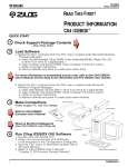
1
Z86C36
ICEBOX
User Manual
UM002202-1001
ZiLOG Worldwide Headquarters • 910 E. Hamilton Avenue • Campbell, CA 95008
Telephone: 408.558.8500 • Fax: 408.558.8300 • www.ZiLOG.com
Z86C36
ICEBOX
This publication is subject to replacement by a later edition. To determine whether a later
edition exists, or to request copies of publications, contact:
ZiLOG Worldwide Headquarters
910 E. Hamilton Avenue
Campbell, CA 95008
Telephone: 408.558.8500
Fax: 408.558.8300
www.ZiLOG.com
Document Disclaimer
ZiLOG is a registered trademark of ZiLOG Inc. in the United States and in other countries. All other products
and/or service names mentioned herein may be trademarks of the companies with which they are associated.
©2001 by ZiLOG, Inc. All rights reserved. Information in this publication concerning the devices,
applications, or technology described is intended to suggest possible uses and may be superseded. ZiLOG,
INC. DOES NOT ASSUME LIABILITY FOR OR PROVIDE A REPRESENTATION OF ACCURACY OF
THE INFORMATION, DEVICES, OR TECHNOLOGY DESCRIBED IN THIS DOCUMENT. ZiLOG
ALSO DOES NOT ASSUME LIABILITY FOR INTELLECTUAL PROPERTY INFRINGEMENT
RELATED IN ANY MANNER TO USE OF INFORMATION, DEVICES, OR TECHNOLOGY
DESCRIBED HEREIN OR OTHERWISE. Except with the express written approval of ZiLOG, use of
information, devices, or technology as critical components of life support systems is not authorized. No
licenses are conveyed, implicitly or otherwise, by this document under any intellectual property rights.
UM002202-1001
Z86C36
ICEBOX
iii
Table of Contents
Table of Contents . . . . . . . . . . . . . . . . . . . . . . . . . . . . . . . . . . . . . . . . . . . . iii
List of Figures . . . . . . . . . . . . . . . . . . . . . . . . . . . . . . . . . . . . . . . . . . . . . . . .v
List of Tables . . . . . . . . . . . . . . . . . . . . . . . . . . . . . . . . . . . . . . . . . . . . . . . vii
Preface . . . . . . . . . . . . . . . . . . . . . . . . . . . . . . . . . . . . . . . . . . . . . . . . . . . . . ix
Introduction . . . . . . . . . . . . . . . . . . . . . . . . . . . . . . . . . . . . . . . . . . . . . . . . . .1
Overview . . . . . . . . . . . . . . . . . . . . . . . . . . . . . . . . . . . . . . . . . . . . . . . . . .1
ICEBOX Features . . . . . . . . . . . . . . . . . . . . . . . . . . . . . . . . . . . . . . . . . . .1
Supported ZiLOG Devices . . . . . . . . . . . . . . . . . . . . . . . . . . . . . . . . .2
Hardware Specifications . . . . . . . . . . . . . . . . . . . . . . . . . . . . . . . . . . . . . .4
Operating Conditions . . . . . . . . . . . . . . . . . . . . . . . . . . . . . . . . . . . . .4
Power Requirements . . . . . . . . . . . . . . . . . . . . . . . . . . . . . . . . . . . . .4
Serial Interface . . . . . . . . . . . . . . . . . . . . . . . . . . . . . . . . . . . . . . . . . .4
GUI-Supported Compiler, Assembler Formats . . . . . . . . . . . . . . . . . . . .4
Kit Contents . . . . . . . . . . . . . . . . . . . . . . . . . . . . . . . . . . . . . . . . . . . . . . .5
Additional Items Not Supplied . . . . . . . . . . . . . . . . . . . . . . . . . . . . . .5
Optional Recommended Item . . . . . . . . . . . . . . . . . . . . . . . . . . . . . .6
Computer Requirements . . . . . . . . . . . . . . . . . . . . . . . . . . . . . . . . . . . . . .6
Minimum Requirements . . . . . . . . . . . . . . . . . . . . . . . . . . . . . . . . . . .6
Contacting ZiLOG Customer Support . . . . . . . . . . . . . . . . . . . . . . . . . . .7
Setup and Installation . . . . . . . . . . . . . . . . . . . . . . . . . . . . . . . . . . . . . . . . . .9
Hardware Installation . . . . . . . . . . . . . . . . . . . . . . . . . . . . . . . . . . . . . . . .9
Quick Installation Instructions . . . . . . . . . . . . . . . . . . . . . . . . . . . . . .9
Complete Installation Instructions . . . . . . . . . . . . . . . . . . . . . . . . . .12
Set Power Jumper . . . . . . . . . . . . . . . . . . . . . . . . . . . . . . . . . . . . . . .12
Installing a New ICE Chip . . . . . . . . . . . . . . . . . . . . . . . . . . . . . . . .16
Software Installation . . . . . . . . . . . . . . . . . . . . . . . . . . . . . . . . . . . . . . . .18
ICEBOX Operation . . . . . . . . . . . . . . . . . . . . . . . . . . . . . . . . . . . . . . . .18
Resetting . . . . . . . . . . . . . . . . . . . . . . . . . . . . . . . . . . . . . . . . . . . . . .19
Table of Contents
UM002202-1001
Z86C36
ICEBOX
iv
LED Operation . . . . . . . . . . . . . . . . . . . . . . . . . . . . . . . . . . . . . . . .
Jumper Settings . . . . . . . . . . . . . . . . . . . . . . . . . . . . . . . . . . . . . . . .
Overview . . . . . . . . . . . . . . . . . . . . . . . . . . . . . . . . . . . . . . . . . . . . . . . . . . .
Using ZDS . . . . . . . . . . . . . . . . . . . . . . . . . . . . . . . . . . . . . . . . . . . . . . .
Select the ICEBOX . . . . . . . . . . . . . . . . . . . . . . . . . . . . . . . . . . . . .
Open a Project and Add Files . . . . . . . . . . . . . . . . . . . . . . . . . . . . .
Available Debug Windows . . . . . . . . . . . . . . . . . . . . . . . . . . . . . . . . . .
Appendix A: Troubleshooting Guide . . . . . . . . . . . . . . . . . . . . . . . . . . . .
Introduction . . . . . . . . . . . . . . . . . . . . . . . . . . . . . . . . . . . . . . . . . . . . . .
Error Opening Serial Port . . . . . . . . . . . . . . . . . . . . . . . . . . . . . . . . . . .
Counter Jumps to Unexpected Address . . . . . . . . . . . . . . . . . . . . . . . .
ZDS Error Messages . . . . . . . . . . . . . . . . . . . . . . . . . . . . . . . . . . . . . . .
Can Not Open Windows . . . . . . . . . . . . . . . . . . . . . . . . . . . . . . . . .
Out of Synchronization with the Emulator . . . . . . . . . . . . . . . . . . .
Appendix B: ASCII Character Set . . . . . . . . . . . . . . . . . . . . . . . . . . . . . .
Appendix C: Problem/Suggestion Report Form . . . . . . . . . . . . . . . . . . .
Glossary . . . . . . . . . . . . . . . . . . . . . . . . . . . . . . . . . . . . . . . . . . . . . . . . . . . .
Index. . . . . . . . . . . . . . . . . . . . . . . . . . . . . . . . . . . . . . . . . . . . . . . . . . . . . . .
UM002202-1001
19
20
23
23
23
26
29
31
31
31
32
32
32
33
35
41
43
47
Table of Contents
Z86C36
ICEBOX
v
List of Figures
Figure 1.
Figure 2.
Figure 3.
Figure 4.
Figure 5.
Figure 6.
Figure 7.
Figure 8.
Figure 9.
Figure 10.
List of Figures
Hook-Up Diagram . . . . . . . . . . . . . . . . . . . . . . . . . . . . . . . .10
Z86C36 ICEBOX External Top View . . . . . . . . . . . . . . . . 11
J1 Jumper Schematic . . . . . . . . . . . . . . . . . . . . . . . . . . . . . 13
ICE Chip Installation . . . . . . . . . . . . . . . . . . . . . . . . . . . . .17
Closing the ICE Chip Locking Lever . . . . . . . . . . . . . . . . .18
New Project Dialog Box . . . . . . . . . . . . . . . . . . . . . . . . . . .24
Emulator Configuration Dialog Box . . . . . . . . . . . . . . . . . .25
Project Viewer Window . . . . . . . . . . . . . . . . . . . . . . . . . . . 27
Insert Files into Project Dialog Box . . . . . . . . . . . . . . . . . .27
Project Viewer Window with File . . . . . . . . . . . . . . . . . . . 28
UM002202-1001
Z86C36
ICEBOX
vi
This page intentionally left blank.
UM002202-1001
List of Figures
Z86C36
ICEBOX
vii
List of Tables
Table 1.
Table 2.
Table 3.
Table 4.
Table 5.
List of Tables
Z86C5020GSE ICE Chip Supported Products
(Z86C3500ZEM Target Emulator Selection) . . . . . . . . . . . .2
Z86C5120GSE ICE Chip Supported Products
(Z86C3600ZEM Target Emulator Selection) . . . . . . . . . . . 2
Front LED Assignments . . . . . . . . . . . . . . . . . . . . . . . . . . .19
Jumper Settings . . . . . . . . . . . . . . . . . . . . . . . . . . . . . . . . . .29
ASCII Character Set . . . . . . . . . . . . . . . . . . . . . . . . . . . . . .35
UM002202-1001
Z86C36
ICEBOX
viii
This page intentionally left blank.
UM002202-1001
List of Tables
Z86C36
ICEBOX
ix
Preface
We recommend that you read and understand everything in this manual
before setting up and using the product. However, we recognize that users
have different styles of learning. Therefore, we have designed this manual
to be used either as a how-to procedural manual or a reference guide to
important data.
The following conventions have been adopted to provide clarity and ease
of use:
•
Times 10-point all-caps is used to highlight the following items:
– commands, displayed messages
– menu selections, pop-up lists, button, fields, or dialog boxes
– modes
– pins and ports
– program or application name
– instructions, registers, signals and subroutines
– an action performed by the software
– icons
•
Courier Regular 10-point is used to highlight the following
items
– bit
– software code
– file names and paths
– hexadecimal value
UM002202-1001
Preface
Z86C36
ICEBOX
x
•
Grouping of Actions Within a Procedure Step
Actions in a procedure step are all performed on the same window or
dialog box. Actions performed on different windows or dialog boxes
appear in separate steps.
UM002202-1001
Preface
Z86C36
ICEBOX
xi
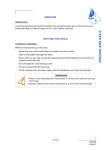
Electrical
Safeguards
Follow the precautions listed below to avoid permanent damage to the
emulator.
1. Always use a grounding strap to prevent damage resulting from
electrostatic discharge (ESD).
2. Power-Up Precautions.
a. Ensure that all power to the emulator and the target application (if
any) is turned OFF.
b. Connect the target pod to the target application (if any).
c. Power up the emulator, then press the RESET button.
d. Power up the target application (if any).
3. Power-Down Precautions.
When powering down, follow this procedure in the precise order
shown below:
a. Halt emulation.
b. In ZDS select Reset from the Build or Debug Menu.
c. Power down the target application board (if any).
d. Remove the target pod.
e. Power down the emulator.
Preface
UM002202-1001
Z86C36
ICEBOX
xii
Notes:
1. Refer to the “Precaution List” section of the Product Information
sheet for additional operating precautions specific to various devices.
2. Do not leave the emulator powered up with the RS-232C cable
connected to a powered-down PC.
3. Before inserting target pod into target application board, refer to
Chapter 2 to determine appropriate jumper selections and options.
UM002202-1001
Preface
Z86C36
ICEBOX
1
1 Introduction
OVERVIEW
Congratulations for selecting a fine development tool! The Z86C36
ICEBOX provides in-circuit emulation for the Z8 family of UART
controllers. The ICEBOX consists of an emulation daughter board that is
plugged into a 32-MHz motherboard using P1 and P2 headers. The
Z86C50 ICE chip is used as the emulation processor for devices with less
than or equal to 32K of code memory. The Z86C51 ICE chip is used as
the emulation processor for devices with 64K of code memory, that is,
Z86C36 and Z86C46.
The 32 MHz motherboard has been modified for 64 K operation and
provides host communication interface, control processor, I/O space
decoding, and LED indicator. The ICEBOXes are designed to be used
with ZiLOG Developers Studio, giving the user a total package to write,
edit, and debug their applications.
ICEBOX FEATURES
Key features of the Z86C36 ICEBOX include:
•
•
•
Supports up to 64 K of ROM
•
The user can choose to power the Ice chip from either the ICEBOX or
target board
•
Supports UART devices that operate up to 16.384 MHz
UM002202-1001
The capability to vary the operating voltage from 3.0–5.0 V
Supports in-circuit emulation on target systems that operate from
3.0–5.5 V
Introduction
Z86C36
ICEBOX
2
•
Emulates and supports all the features and functions for a specified
Z8 UART microcontroller
•
Multitasking allows the user to use other Windows applications while
ZiLOG Developer Studio (ZDS) is running
Supported ZiLOG Devices
Table 1 shows products supported by the Z86C5020GSE ICE chip.
Table 2 shows the products supported by the Z86C5120GSE ICE chip.
Table 1. Z86C5020GSE ICE Chip Supported Products (Z86C3500ZEM
Target Emulator Selection)
Packages
Emulation
OTP
Required Accessories
28 PDIP
Z86C34–C35
N/A
28 PDIP emulation pod
28 SOIC
Z86C34–C35
N/A
28 PDIP emulation pod and a DIP to SOIC
conversion adapter from Emulation Technology
(AS-DIP-6-028-S003-1 or AS-DIP-6-028-S003-2)
28 PLCC
Z86C34–C35
N/A
28 PLCC emulation pod
40 PDIP
Z86C44–C45
N/A
40 PDIP emulation pod
44 PLCC
Z86C44–C45
N/A
44 PLCC emulation pod
44 QFP
N/A
N/A
N/A
Table 2.
Z86C5120GSE ICE Chip Supported Products (Z86C3600ZEM
Target Emulator Selection)
Packages
Emulation
OTP
Required Accessories
28 PDIP
Z86C36
N/A
28 PDIP emulation pod
UM002202-1001
Introduction
Z86C36
ICEBOX
3
Table 2.
Z86C5120GSE ICE Chip Supported Products (Z86C3600ZEM
Target Emulator Selection) (Continued)
Packages
Emulation
OTP
Required Accessories
28 SOIC
Z86C36
N/A
28 PDIP emulation pod and a DIP to SOIC
conversion adapter from Emulation Technology (ASDIP-6-028-S003-1 or AS-DIP-6-028-S003-2)
28 PLCC
Z86C36
N/A
28 PLCC emulation pod
40 PDIP
Z86C46
N/A
40 PDIP emulation pod
44 PLCC
Z86C46
N/A
44 PLCC emulation pod
Notes: The Z86C3600ZEM becomes the Z86C3500ZEM when you use
a Z86C50 ICE chip.
Introduction
UM002202-1001
Z86C36
ICEBOX
4
HARDWARE SPECIFICATIONS
Operating Conditions
Operating Humidity:
10%-90% RH (Noncondensing)
Operating Temperature:
20 °C ±10 °C
Clocks:
The control processor operates at 7.3728
Mhz; the emulation processor operates at
16.384 Mhz
Serial Baud Rate:
57,600 bps
Power Requirements
This ICEBOX requires an external 5VDC power supply.
Operating Voltage (Input):
+4.75 VDC to +5.25 VDC Max
(+5.0 VDC typical)
Operating Voltage (Target):
+3.0 VDC to +5.5 VDC Max
Operating Current:
2.5 A typical (maximum 3.0 A)
Serial Interface
ZiLOG Developer Studio communicates with the Z86C36 ICEBOX using
a DB25, RS-232 and DCE cable (TxD, RxD only).
GUI-SUPPORTED COMPILER, ASSEMBLER FORMATS
The ICEBOX supports object (binary or Intel hex) code files produced by
ZiLOG Developer Studio (ZDS) and ZiLOG Macro Cross Assembler
(ZMASM).
UM002202-1001
Introduction
Z86C36
ICEBOX
5
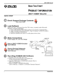
KIT CONTENTS
The ICEBOX kit contains one of each of the following items:
•
•
•
•
•
•
•
•
•
•
Z86C36 ICEBOX
40 PDIP emulation pod with cable ZiLOG: 93C0024-001
44 PLCC emulation pod ZiLOG PC: 99C0273-001
28 PDIP emulation pod ZiLOG PC: 99C0742-001
28 PLCC emulation pod ZiLOG PC: 99C0512-001
Power Cable with Banana Plugs
RS-232 Serial Cable, DB 25
ZiLOG Developer Studio Installation CD
Z86C36 ICEBOX User Manual
ZiLOG Developer Studio manual contained on the ZDS installation
CD-ROM.
Note: If the ZDS CD-ROM does not contain the manual, it can be
downloaded from the ZiLOG web page at www.zilog.com.
Additional Items Not Supplied
The following item is required but are not currently supplied in the
ICEBOX kit:
•
Introduction
A source of power (+5 VDC typical) for the ICEBOX. This can be a
laboratory power supply with current rating of at least 2.5 ampere.
UM002202-1001
Z86C36
ICEBOX
6
Optional Recommended Item
The following items are recommended:
•
Your target design. The target design is a wire-wrapped or printed
circuit prototype that includes a socket for the target device that the
ICEBOX cable/pod plugs into.
•
C-Compiler
Note: Contact a ZiLOG Sales Office or Distributor to order a copy of the
Z8 C-Compiler. Refer to our website for a representative near you:
http://www.zilog.com/sales/.
•
•
Oscilloscope
Logic Analyzer
COMPUTER REQUIREMENTS
Minimum Requirements
•
•
•
•
•
IBM PC (or 100-percent compatible) Pentium based machine
•
•
•
RS-232 COM Port
UM002202-1001
75 MHz or more with 16 MB RAM
VGA Video Adapter
Hard Disk Drive (12 MB free space)
CD-ROM Drive (a CD-ROM drive is not needed if you download
ZDS from the web at www.zilog.com)
Mouse or Pointing Device
Microsoft Windows 95/98/NT
Introduction
Z86C36
ICEBOX
7
The following enhancements to the minimum requirements are
recommended:
•
•
•
166-MHz IBM PC
SVGA video adapter
Printer
CONTACTING ZILOG CUSTOMER SUPPORT
ZILOG has a worldwide customer support center located in Austin,
Texas. The customer support center is open from 7 a.m. to 7 p.m. Central
Time.
The customer support toll-free number for the United States and Canada
is 1-877-ZiLOGCS (1-877-945-6427). For calls outside of the United
States and Canada dial 512-306-4067. The FAX number to the customer
support center is 512-306-4072. Customers can also contact the support
center through our website at http://www.zilog.com/support/.
For valuable information about hardware and software development tools,
go to ZiLOG home page at http://www.zilog.com. The latest released
version of the ZDS can be downloaded from this site.
Introduction
UM002202-1001
Z86C36
ICEBOX
8
This page intentionally left blank.
UM002202-1001
Introduction
Z86C36
ICEBOX
9
2 Setup and Installation
HARDWARE INSTALLATION
Before installing the hardware, refer to Figure 1 for a diagram on
connecting the ICEBOX to a PC and power supply. Figure 2 provides
option jumper locations.
Quick Installation Instructions
To install the hardware using a bench power supply, perform the
following.
1. Set the correct jumper setting for powering the ICE chip and target
board. See Set Power Jumper on page 12.
2. Connect the power supply to the emulator and ensure it is set to
provide + 5.0 V and 2.5 A.
3. Connect the serial cable to the PC.
4. Connect the ICEBOX to the target board (if performing in-circuit
emulation).
5. Set up the oscillator and option jumpers.
6. Select the ICE chip that you want to emulate.
7. Power up the ICEBOX.
UM002202-1001
Setup and Installation
Z86C36
ICEBOX
10
-+
Figure 1. Hook-Up Diagram
Note: Each ICEBOX is shipped with a 16.384 MHz oscillator. The user
can also use the target’s oscillator or a crystal/ ceramic resonator
to clock the ICE chip, for more information see Jumper Settings
on page 20.
UM002202-1001
Setup and Installation
Z86C36
ICEBOX
11
Power
RS-232C
Debug
pins
Reset
Logic analyzer connector*
Voltage
adjuster
J1
ICE chip ziff
socket
J3
J2
Oscillator
J5
J6
J7
U1
Reset
Target Pod
LEDS
*This is not supported.
Figure 2.
Setup and Installation
Z86C36 ICEBOX External Top View
UM002202-1001
Z86C36
ICEBOX
12
Complete Installation Instructions
The following procedures illustrate a complete step-by-step guide on
installing the ICEBOX.
Set Power Jumper
The Z86C36 ICEBOXes allow the user to power the ICEBOXes and
target from a variety of different sources. Before powering the ICEBOX
the user should select the power configuration.
Caution: The procedures below must be followed exactly as described.
Before beginning the procedures study Figure 3, which shows a
schematic of the J1 power jumper. Failure to follow the procedures will result in total damage to the ICEBOX or target.
Choose from one of the following options when selecting the power
source:
•
Jumper pin 1 to pin 2 to power the ICE chip with the ICEBOX’s
adjustable regulator
•
Jumper pin 3 to pin 4 to power target with the ICEBOX’s adjustable
regulator
•
Jumper pin 1 to pin 2 and pin 3 to pin 4 to power both the ICE chip
and target from the ICEBOX’s adjustable regulator
•
Jumper pin 2 to pin 4 to power the ICE chip from the target
Note: When powering the target from the ICEBOX ensure that the
target’s power supply is disconnected.
UM002202-1001
Setup and Installation
Z86C36
ICEBOX
13
1
2
ICE chip
ICEBOX Adjustable
Voltage Regulator
3
Figure 3.
4
Target
J1 Jumper Schematic
Connect the Power Supply
1. If the power supply allows voltage adjustment:
– Turn the power supply on and adjust it to +5 V
– Adjust the limiting adjustment, if present, to at least 2.5 A
2. Turn the supply off.
3. Locate the power cable (red wire, black wire, and banana plugs on the
other end). Plug in the black banana plug into the black jack on the
power supply (labeled COM, GND, or with the ground symbol). Plug
the red plug into the red jack on the power supply (labeled +, + V or
+5 V).
4. Plug the white connector on the other end of the cable into the
matching 4-pin connector on the back side of the ICEBOX. This
connection is keyed to ensure against an improper connection.
Note: The ZiLOG Power Supply Accessory Kit (ZPS05V00ZAC),
which is sold separately, provides a fixed-5 V Universal Output
Power Supply, accepts 110 V to 220 V AC input, and includes a
power cable and an in-line jack cable.
Caution: Always check the supply voltage before plugging in the power
cord.
Setup and Installation
UM002202-1001
Z86C36
ICEBOX
14
Connect the Serial Cable to the PC
Locate the serial cable. Connect the male end to the female connector on
the back of the ICEBOX, and the female end to either the COM1, COM2,
COM3, or COM4 connector of the host PC, see Figure 1.
Note: If connector availability is limited to a 9-pin COM1 through
COM4, then use either a different cable or a 25-pin to 9-pin
converter. This converter is available at any electronics store for a
nominal fee.
Connect to the Design
Perform the following steps to connect to the target design:
Caution: Wear a properly grounded wrist strap or similar ESD protection
before continuing.
1. Locate the emulation cable for the device.
2. Plug the cable into the target device. Ensure that the pin 1 marking (as
indicated by the red mark on the ribbon cable) matches pin 1 on the
target board.
3. Plug the other end of the cables into target pod on top of the
ICEBOX. See Figure 2 for the location of the target pod.
4. Select the power source for the ICE chip by configuring the J1
jumper. See Table 4 for more information on jumper settings and
Figure 2 for the location of the J1 jumper.
5. If the target and ICEBOX are using separate power supplies, ensure
that the ICE chip voltage matches the target’s device voltage. Adjust
the voltage by performing the following steps:
a. Measure the voltage of your target.
b. Locate the voltage adjuster on top of the ICEBOX. See Figure 2
for the location of the voltage adjuster
UM002202-1001
Setup and Installation
Z86C36
ICEBOX
15
c. Attach the voltmeter lead to either pin 1 or 3 on the J1 jumper and
ground.
d. Power the ICEBOX with the target device disconnected.
e. Turn the voltage adjuster’s screw until the voltmeter’s read-out
matches the target device’s voltage.
Caution: Failure to match the target devices voltage with the ICE chip’s
voltage could result in damage to the ICEBOX, target device, or
ICE chip.
Power the ICEBOX
If anything unusual (such as an unexpected sound and/or smell) occurs
when turning on the power supply, turn off the power supply and check
the setting for the J1 jumper. See Set Power Jumper on page 12. If the
power supply allows voltage adjustment, adjust it again to +5 V. The
power supply output may measure less than +5 V because of the load of
the ICEBOX. If your power supply has a current meter, ensure that the
ICEBOX is drawing within the rated current.
After power-up, press the RESET button to reset the ICE chip. (Pressing
the RESET button avoids bus contention on the I/O lines.) If the ICEBOX
is not powering your design through the VCC pin, turn on the power
supply of the design.
Caution: If your design already has a power supply, do not power your
design from the ICEBOX VCC pin.
When powering down, follow the procedure described below:
1. Halt emulation.
2. In ZDS select Reset from the Build or Debug Menu.
3. Power down the target application board (if using its own power
supply).
4. Power down the ICEBOX.
Setup and Installation
UM002202-1001
Z86C36
ICEBOX
16
Note: Refer to the complete Electrical Safeguards shown in the preface
of this manual.
Installing a New ICE Chip
The Z86C36 ICEBOX comes with the Z86C51 ICE chip. Under ordinary
circumstances, the user should never have to remove this ICE chip. If for
some reason the ICE chip needs to be replaced, follow the procedures
below. See Figure 4 and Figure 5 for more information.
Note: Replace the Z86C51 ICE chip with the Z86C50 ICE chip to
support devices with 32K code size or less.
Caution: Failure to follow the procedures below could result in damage
to the ICEBOX.
Perform the following steps to replace the ICE chip.
1. Disconnect all power to the ICEBOX
2. Move the ICEBOX ziff socket labeled U1 to the upright position and
remove the ICE chip. See Figure 2 for the location of the ziff socket.
3. Place the new ICE chip into the U1 ziff socket. Ensure that the ICE
chip’s pin 1 matches pin 1 on the U1 ziff socket.
4. Close the ziff socket locking lever.
Note: A dot in the corner of the processor indicates the chip’s pin 1
location.
UM002202-1001
Setup and Installation
Z86C36
ICEBOX
17
Figure 4.
Setup and Installation
ICE Chip Installation
UM002202-1001
Z86C36
ICEBOX
18
Figure 5.
Closing the ICE Chip Locking Lever
SOFTWARE INSTALLATION
For more information on installing ZDS, refer to the user manual that is
included on the installation CD-ROM or download ZDS literature from
the ZiLOG web page at www.zilog.com.
ICEBOX OPERATION
The following topics guide the user on how to operate the ICEBOX and
configure jumper settings.
UM002202-1001
Setup and Installation
Z86C36
ICEBOX
19
Resetting
Press the RESET button on the ICEBOX to reset the state of the target
device and the status that was established using ZDS.
For example, the ICEBOX sets the program counter to 000Ch.
After reset, wait until the Ready LED is ON and has finished blinking
before starting ZDS. Refer to the LED Operation section of this chapter
for more details.
Note: Always press the RESET button on the ICEBOX before starting
ZDS.
LED Operation
ZiLOG ICEBOXes use LEDs to communicate the different hardware
states. The following table gives a description of the LEDs. The
ICEBOX’s LED’s are located on the right front of the ICEBOX. See
Table 3.
Table 3. Front LED Assignments
LED
Indication
Description
READY
On
Off
Communicating in Bisync Mode and waiting for command
Communicating in ASCII Mode or executing Bisync command
RUN
On
Off
Running user code
Not running user code
OTP
On
Off
The ICEBOX is performing OTP programming
The ICEBOX completed OTP programming
PWR
On
Off
Blink
ICEBOX is powered up and Self Test is completed
Power is off
ICEBOX is self-testing
Setup and Installation
UM002202-1001
Z86C36
ICEBOX
20
Jumper Settings
Table 4 lists jumper setting that the are easily configured by the user. See
Figure 2 for the location of the jumpers.
Table 4.
Jumper Settings
Jumper
Pin
Position
Description
J1
1-2
In
Powers the ICE chip with ICEBOX’s adjustable voltage
regulator (default), for more information see Figure 3
J1
3-4
In
Powers the Target with ICEBOX’s adjustable voltage regulator
J1
2-4
In
Target powers the ICE chip
J2
1-2
In
Y2 Crystal to XTAL2
J2
2-3
In
User Crystal to XTAL2
J3
1-2
In
Y2 Crystal to XTAL1
J3
2-3
In
User Crystal to XTAL1
J3
2-4
In
Canned Oscillator to XTAL1 (Default)
J5
1-2
In
Not installed (factory settings)
J6
2-4
In
Enable if P3.4 used for external memory/DM (see note)
J6
2-3
In
P3.4 not used (default)
J6
1-2
In
Ground signal
J7
1-2
In
Default setting
J7
2-3
In
Output of PAL (Programable Array Logic)/not used
Note: Port 3 pin 4 can be used as an output pin or an external memory
indicator. If P3.4 is used for external memory and not data
memory, then jumper pin 2 to pin 4 on the J6 jumper.
UM002202-1001
Setup and Installation
Z86C36
ICEBOX
21
The user can adjust the voltage of the ICE chip to match the target’s
voltage using the ICEBOX’s R55 Voltage Adjuster. See Figure 2 for the
location of the voltage adjuster.
Setup and Installation
UM002202-1001
Z86C36
ICEBOX
22
This page intentionally left blank.
UM002202-1001
Setup and Installation
Z86C36
ICEBOX
23
3 Overview
USING ZDS
This ICEBOX is fully compatible with ZiLOG Developer Studio (ZDS)
software. The following steps briefly describe the procedures necessary to
setup and create projects with the Z86C36 ICEBOX. A summary of the
ICEBOX’s available debug windows is also included at the end of this
chapter.
For more detailed information on using ZDS, refer to the ZDS User
Manual (in PDF format) located on the installation CD-ROM, or
download the latest information from our web site at www.zilog.com.
Select the ICEBOX
Perform the following steps to select the ICEBOX and create a new
project:
1. Open ZDS by selecting Start>Programs>Zilog Developer Studio>
ZDS.
2. Choose New Project from the File menu. The New Project dialog box
appears as show in Figure 6.
Note: If the project has already been created, select Target from the
Project menu and perform the following steps that are applicable
for the ZiLOG MCU Database dialog box.
UM002201-0301
Overview
Z86C36
ICEBOX
24
Z86C3500ZEM
Figure 6.
New Project Dialog Box
3. Select Family in the Selection by field.
4. Select Z8 from the Master pop-up list.
5. Select a microcontroller from the Z8 family in the Project Target popup list.
6. Select Z86C3500ZEM or Z86C3600ZEM in the Emulator pop-up
list.
Note: The Z86C3600ZEM becomes the Z86C3500ZEM when you use a
Z86C50 ICE chip.
7. Click on the browse button (...) in the Project Name field. The New
Project Browser dialog box appears.
8. Enter the project file name and select a path in the New Project
Browse dialog box.
UM002201-0301
Overview
Z86C36
ICEBOX
25
Note: All build output files, such as linker and assembly files are saved
in the same directory as the project.
9. Click Save. The project name appears in the Project Name field in the
New Project dialog box.
10. Click on Chip Data to view the microcontroller specifications.
Note: Fields in the Chip Data page are read-only and can not be
modified.
11. Click OK. The new project is saved as the name specified in the New
Project Browse dialog box.
12. Select Emulator Configuration from the Project menu. The Emulator
Configuration dialog box appears, as shown in Figure 7.
Figure 7.
Overview
Emulator Configuration Dialog Box
UM002201-0301
Z86C36
ICEBOX
26
13. Ensure that Emulator is selected in the Module field.
14. Select the port the ICEBOX is connected to from the Port pop-up list.
15. Select 57600 from the Baud Rate pop-up list.
16. Click OK to close and apply the Emulator Configuration options.
17. Select Save Project from the File menu to save the emulator
configuration setting.
Open a Project and Add Files
A previously created project has the following attributes saved with it:
•
•
•
Target settings
Assembler and Linker settings for the specified target
Source files (including header files)
Note: Use the Project Viewer window to view and access the various
files in any given project.
Perform the following steps to open a previously created project:
1. Select Open Project from the File menu. The Open Project dialog box
appears.
2. In the Open Project dialog box, select the previously created project.
The project appears in the Project Viewer window, as shown in
Figure 8.
UM002201-0301
Overview
Z86C36
ICEBOX
27
Figure 8.
Project Viewer Window
Add an Existing File
Perform the following steps to add an existing file to a project:
1. Select Add to Project>Files from the Project menu. The Insert Files
into Project dialog box appears, as shown in Figure 9.
Figure 9.
Insert Files into Project Dialog Box
2. Select the file to add to the project.
Overview
UM002201-0301
Z86C36
ICEBOX
28
3. Click Open. The file appears in the Project Viewer window, as shown
in Figure 10.
Figure 10.
Project Viewer Window with File
4. Double-click on the file in the Project Viewer window. The file
appears in the ZDS main Edit window.
Note: In some cases, non-editable files, such as .obj files need to be
included in a project. These files are displayed in the source file
list, but cannot be opened. When the project is built, these files are
automatically linked.
5. Select Update All Dependencies from the Build menu. The
Dependencies folder list in the Project Viewer window is updated.
Add a New File
1. Select Add to Project>New from the Project menu. The Insert New
Files Into Project dialog box appears.
2. Type a file name in the File Name field.
3. Click Open. The new file name appears in the Project Viewer window
with a .asm suffix, and a blank Edit window also appears.
Note: Header and Included files do not have to be added. The program
detects those called by the source code.
UM002201-0301
Overview
Z86C36
ICEBOX
29
#8#+.#$.'&'$7)9+0&195
Table 5 lists the debug windows that are available using ZDS.
Table 5.
Debug Windows
Updated values display in red
Window
Function
Watch
•
Shows the symbols and the contents of the registers(see the
ZDS user manual for more information)
Z8 Standard Registers
•
•
Shows the contents of the Z8 standard registers
Code Memory
Disassembly
Overview
Allows the user to monitor, edit, and download a .ld file
or a .hex file into Code Memory from generated assembly
source code
•
Tracks a specific address entered in the Code Address edit
box
•
Shows code memory along with the corresponding
disassembled code
•
Allows the user to edit, and download a file.ld or file.hex
into the Code memory
•
•
Follows the program counter
•
Accesses the disassembly of code at the address specified in
the Code Address field
•
The Disassembly window is automatically displayed when
debugging hex code or whenever there is no corresponding
source file available at the address specified by the program
counter
Provides a complete scroll down with this window,
however the scroll up is limited
UM002201-0301
Z86C36
ICEBOX
30
Table 5.
Debug Windows (Continued)
Updated values display in red
Window
Function
Z8 Register File
•
Shows all Z8 internal and external registers, all RAM
pointer and data registers, status registers and status flags,
and stacks
Monitor and edit write-able registers in this window
Z8 Expanded Register
•
•
•
Monitor and edit write-able registers directly in this window
by selecting a specific bank tab
•
•
•
Modify and view working registers in this window
Working Registers
Timer Counter Registers
Ports Register
UM002201-0301
Displays the Z8 Expanded Register banks that are specified
in the configuration
Modify and view the timer/counter registers in this window
Monitor and edit port registers in this window
Overview
Z86C36
ICEBOX
31
Appendix A: Troubleshooting Guide
INTRODUCTION
Before contacting a ZiLOG representative or submitting a Problem
Report, please follow these simple steps. Also, check the Precautions and
Limitations sections in the Product Information document included with
the emulator to eliminate other possible known problems. If a hardware
failure is suspected, contact a local ZiLOG representative for assistance.
ERROR OPENING SERIAL PORT
If the initial ZiLOG screen is not appearing after selecting the COM port
and the screen message displays Time-out while reading:
1. Check the RS-232C cable connection and communication port
selection in ZDS. See Select the ICEBOX on page 23 for more
information on how to configure the host PC’s port.
2. Reset the emulator and ZDS.
3. Try connecting another cable.
4. Check if transmit/receive signals need to be swapped.
Note: On some DB9 connectors for the COM ports, the transmit/receive
signal may be swapped and a Null Modem adapter may be
required.
5. Ensure that the power supply is connected, is turned on, and power is
available.
6. Ensure that the power supply is set at the correct voltage.
UM002202-1001
Appendix A: Troubleshooting Guide
Z86C36
ICEBOX
32
7. Ensure that the J1 power jumper has been properly configured. See
Set Power Jumper on page 12 for more information on setting the J1
jumper.
8. Check if power supply is supplying the required current (2.5 A
typical) to the emulator.
9. Check selected the port using another application or select another
COM port.
10. After resetting the emulator, wait a minimum of 5 seconds before
running ZDS.
COUNTER JUMPS TO UNEXPECTED ADDRESS
Any instruction other than a DI instruction is used to disable interrupts.
Possible causes include:
•
•
•
The stack overflows into the general register locations.
•
Unintialized interrupt vector is activated. The interrupt vector is not
set to the interrupt handler.
Extra POP, PUSH, IRET, or RET is encountered (stack unbalanced).
Program resets repeatedly.
– Program counter rolls over from value FFFF to 0000 and
proceeds back to the beginning of program.
– Watch-Dog Timer (WDT) is not initialized or refreshed.
ZDS ERROR MESSAGES
Can Not Open Windows
If this message appears while attempting to open a window ZDS, there
may not be enough memory within the Microsoft Windows environment
UM002202-1001
Appendix A: Troubleshooting Guide
Z86C36
ICEBOX
33
to properly run ZDS. Try closing the other active applications or exit and
re-enter the Microsoft Windows environment.
Out of Synchronization with the Emulator
This message appears whenever communication between the emulator
and the PC is interrupted.
1. Ensure that the power cable is connected.
2. Ensure that the RS-232C cable is connected.
3. Change the baud rate setting (default is 19200). A lower setting
usually improves communications reliability.
4. Reestablish communication between ZDS and the emulator. See the
ZDS on-line help for more information on establishing
communication with an emulator.
Appendix A: Troubleshooting Guide
UM002202-1001
Z86C36
ICEBOX
34
This page intentionally left blank.
UM002202-1001
Appendix A: Troubleshooting Guide
Z86C36
ICEBOX
35
Appendix B: ASCII Character Set
Table 6. ASCII Character Set
Graphic
Decimal
Hexadecimal
0
0
Null
1
1
Start Of Heading
2
2
Start Of Text
3
3
End Of Text
4
4
End Or Transmission
5
5
Enquiry
6
6
Acknowledge
7
7
Bell
8
8
Backspace
9
9
Horizontal Tabulation
10
A
Line Feed
11
B
Vertical Tabulation
12
C
Form Feed
13
D
Carriage Return
14
E
Shift Out
15
F
Shift In
16
10
Data Link Escape
17
11
Device Control 1
18
12
Device Control 2
UM002202-1001
Comments
Appendix B: ASCII Character Set
Z86C36
ICEBOX
36
Table 6. ASCII Character Set (Continued)
Graphic
Decimal
Hexadecimal
Comments
19
13
Device Control 3
20
14
Device Control 4
21
15
Negative Acknowledge
22
16
Synchronous Idle
23
17
End Of Block
24
18
Cancel
25
19
End Of Medium
26
1A
Substitute
27
1B
Escape
28
1C
File Separator
29
1D
Group Separator
30
1E
Record Separator
31
1F
Unit Separator
32
20
Space
!
33
21
Exclamation Point
"
34
22
Quotation Mark
#
35
23
Number Sign
$
36
24
Dollar Sign
%
37
25
Percent Sign
&
38
26
Ampersand
’
39
27
Apostrophe
(
40
28
Opening (Left) Parenthesis
)
41
29
Closing (Right) Parenthesis
UM002202-1001
Appendix B: ASCII Character Set
Z86C36
ICEBOX
37
Table 6. ASCII Character Set (Continued)
Graphic
Decimal
Hexadecimal
Comments
*
42
2A
Asterisk
+
43
2B
Plus
,
44
2C
Comma
-
45
2D
Hyphen (Minus)
.
46
2E
Period
/
47
2F
Slant
0
48
30
Zero
1
49
31
One
2
50
32
Two
3
51
33
Three
4
52
34
Four
5
53
35
Five
6
54
36
Six
7
55
37
Seven
8
56
38
Eight
9
57
39
Nine
:
58
3A
Colon
;
59
3B
Semicolon
<
60
3C
Less Than
=
61
3D
Equals
>
62
3E
Greater Than
?
63
3F
Question Mark
@
64
40
Commercial At
Appendix B: ASCII Character Set
UM002202-1001
Z86C36
ICEBOX
38
Table 6. ASCII Character Set (Continued)
Graphic
Decimal
Hexadecimal
Comments
A
65
41
Uppercase A
B
66
42
Uppercase B
C
67
43
Uppercase C
D
68
44
Uppercase D
E
69
45
Uppercase E
F
70
46
Uppercase F
G
71
47
Uppercase G
H
72
48
Uppercase H
I
73
49
Uppercase I
J
74
4A
Uppercase J
K
75
4B
Uppercase K
L
76
4C
Uppercase L
M
77
4D
Uppercase M
N
78
4E
Uppercase N
0
79
4F
Uppercase 0
P
80
50
Uppercase P
Q
81
51
Uppercase Q
R
82
52
Uppercase R
S
83
53
Uppercase S
T
84
54
Uppercase T
U
85
55
Uppercase U
V
86
56
Uppercase V
W
87
57
Uppercase W
UM002202-1001
Appendix B: ASCII Character Set
Z86C36
ICEBOX
39
Table 6. ASCII Character Set (Continued)
Graphic
Decimal
Hexadecimal
Comments
X
88
58
Uppercase X
Y
89
59
Uppercase Y
Z
90
5A
Uppercase Z
[
91
5B
Opening (Left) Bracket
\
92
5C
Reverse Slant
]
93
5D
Closing (Right) Bracket
^
94
5E
Circumflex
_
95
SF
Underscore
‘
96
60
Grave Accent
a
97
61
Lowercase A
b
98
62
Lowercase B
c
99
63
Lowercase C
d
100
64
Lowercase D
e
101
65
Lowercase E
f
102
66
Lowercase F
g
103
67
Lowercase G
h
104
68
Lowercase H
i
105
69
Lowercase I
j
106
6A
Lowercase J
k
107
6B
Lowercase K
1
108
6C
Lowercase L
m
109
6D
Lowercase M
n
110
6E
Lowercase N
Appendix B: ASCII Character Set
UM002202-1001
Z86C36
ICEBOX
40
Table 6. ASCII Character Set (Continued)
Graphic
Decimal
Hexadecimal
Comments
o
111
6F
Lowercase O
p
112
70
Lowercase P
q
113
71
Lowercase Q
r
114
72
Lowercase R
s
115
73
Lowercase S
t
116
74
Lowercase T
u
117
75
Lowercase U
v
118
76
Lowercase V
w
119
77
Lowercase W
x
120
78
Lowercase X
y
121
79
Lowercase Y
z
122
7A
Lowercase Z
{
123
7B
Opening (Left) Brace
|
124
7C
Vertical Line
}
125
7D
Closing (Right) Brace
~
126
7E
Tilde
127
7F
Delete
UM002202-1001
Appendix B: ASCII Character Set
Z86C36
ICEBOX
41
Appendix C: Problem/Suggestion
Report Form
If you experience any problems while operating this product, or if you note any inaccuracies while reading the user manual, please copy this form, fill it out, then mail or
fax it to ZiLOG. We also welcome your suggestions!
Customer Information
Name
Country
Company
Telephone
Address
Fax Number
City/State/ZIP
E-Mail Address
Product InformationReturn Information
Serial # or Board Fab #/Rev. #
ZiLOG, Inc.
Software Version
System Test/Customer Support
Manual Number
910 E. Hamilton Ave., Suite 110, MS 4-3
Host Computer Description/Type
Campbell, CA 95008
Fax Number: (408) 558-8536
Email: [email protected]
Problem Description or Suggestion
Provide a complete description of the problem or your suggestion. If you are reporting a specific
problem, include all steps leading up to the occurrence of the problem. Attach additional pages as
necessary.
_______________________________________________________________________________
______________________________________________________________________________
_______________________________________________________________________________
UM002202-1001
Appendix C: Problem/Suggestion Report
Z86C36
ICEBOX
42
This page intentionally left blank.
UM002202-1001
Appendix C: Problem/Suggestion Report
Z86C36
ICEBOX
43
Glossary
ASCII
American Standard Code of Information
Interchange.
Baud
Unit of measure of transmission capacity.
Binary
Number system based on 2. A binary digit is a bit.
BISYNC
Bidirectional Synchronous Communication
Protocol.
Bit
A digit of a binary system. It has only two possible
values: 0 or 1.
BPS
Bits Per Second. Number of binary digits transmitted
every second during a data-transfer procedure.
Bus
In Electronics, a parallel interconnection of the
internal units of a system that enables data transfer
and control Information.
Byte
A collection of four sequential bits of memory. Two
sequential bytes (8 bits) comprise one word.
COM
Device name used to designate a communication
port.
DIP
Dual In-line Package. The plastic housing designed
to be attached directly to a circuit board or equipment
case.
UM002202-1001
Glossary
Z86C36
ICEBOX
44
Emulation
Process of duplicating the behavior of one product or
part using another medium.
Emulator
An emulation device. For example, an In-Circuit
Emulator (ICE) module duplicates the behavior of
the chip it emulates in the circuit being tested.
GUI
Graphical User Interface. The windows and text that
a user sees on their computer screen when they are
using a program.
ICE
In-Circuit Emulator. A ZiLOG product which
supports the application design process.
Icon
A small screen image representing a specific
element like a document, embedded and linked
objects, or a collection of programs gathered
together in a group.
Initialize
To establish start-up parameters, typically involving
clearing all of some part of the device’s memory
space.
Instruction
Command.
I/O
Input/Output. In computers, the part of the system
that deals with interfacing to external devices for
input or output, such as keyboards or printers.
MCU
Microcontroller or Microcomputer Unit.
OTP
One-Time Programmable.
PC
Personal computer, program counter.
UM002202-1001
Glossary
Z86C36
ICEBOX
45
POP
Retrieve a Value from the Stack.
Port
The point at which a communications circuit terminates at a Network, Serial, or Parallel Interface card.
PUSH
Store a Value In the Stack.
RA
Relative Address.
RAM
Random-Access Memory. A memory that can be
written to or read at random. The device is usually
volatile, which means the data is lost without power.
RS-232C
Electronic Industries Association Standard for
Asynchronous Transmissions Between a Computer
and a Peripheral Device.
SOIC
Small Outline IC.
SVGA
Super Video Graphics Adapter.
TMR
Timer Mode Register.
UART
Universal Asynchronous Receiver Transmitter.
Component or functional block that handles
asynchronous communications. Converts the data
from the parallel format in which it is stored, to the
serial format for transmission.
V
Volt, Overflow Flag.
V CC
Supply Voltage.
Glossary
UM002202-1001
Z86C36
ICEBOX
46
WDT
Watch-Dog Timer. A timer that, when enabled under
normal operating conditions, must be reset within the
time period set within the application (WDTMR
(1,0)). If the timer is not reset, a Power-on Reset
occurs. Some earlier manuals refer to this timer as the
WDTMR.
Word
Amount of data a processor can hold in its registers
and process at one time. A DSP word is often 16 bits.
Given the same clock rate, a 16-bit controller
processes four bytes in the same time it takes an 8-bit
controller to process two.
XTAL
Crystal.
Z8
ZiLOG Chip.
ZDS
ZiLOG Developer Studio. ZiLOG’s program
development environment for Windows 95/98/NT.
Z
locatable object modules for the ZiLOG family of
microcontrollers.
ZMASM
ZiLOG Macro Cross Assembler. ZiLOG’s program
development environment for Windows 3.1.
UM002202-1001
Glossary
Z86C36
ICEBOX
47
Index
A
J
Adjust the voltage 14
Appendix A 31, 35, 41
ASCII Character Set 35
Available Debug Windows 29
jumper settings 18
K
Kit Contents 5
C
Chip Data 25
Choosing the IceChip 15
Clocks 4
Connect to Your Design 14
L
E
O
Error Messages 32
Overview 1
H
P
Header and Included files 28
power supply 13
adjusting 13
problems 15
settings 9
powering down 15
I
Index 47
Insert Files 27
Installation 9, 23
installation instructions 12
LED Operation 19
List of Figures v
List of Tables vii
Q
Quick installation 9
Index
UM002202-1001
Z86C36
ICEBOX
48
R
Requirements 6
RESET 15
Resetting 19
S
Selecting the emulator 23
serial cable 14
Software Installation 18
Software Setup 23
T
Table of Contents iii
Target connectors 11
V
voltage adjuster 14
Z
ZDS
adding files 26
Create a New Project 23
Debug windows 29
New Project 25
obj files 28
Open a project 26
Project Viewer window 28
UM002202-1001
Index
UD[7..0]
<>1E4
<>1A4
10k R25
10k R24
10k R23
C50SZ[2..0]
10k R21
<1A3
10k R22
U1
UD0
UD1
UD2
UD3
UD4
UD5
UD6
UD7
U_P1[7..0]
U_D[7..0]
<3A1
B12
A12
C10
B11
A11
B10
C9
A10
C50SZ0
C50SZ1
C50SZ2
nIRQ3
B9
A9
C8
nIRQ3
M10
L9
J1
nIRQ4
nRESET
ICRAM
U_P0[7..0]
<3A3
SMR
>1A4
U_P2[7..0]
ICRAM
2
4
6
8
10
12
14
16
18
20
22
24
26
28
30
32
34
36
38
40
42
44
46
48
50
52
54
56
58
60
62
64
66
68
70
72
74
76
78
80
TARGET CONNECTION
>1A4
nU_RESET
<3A1
>3A2
>1E1
>3A2
<3A1
T_P37
T_P30
U_P3[7..0]
U_P37
U_P30
P3
1 U_RW
nU_DS
3
U_P25
5
U_P24
7
U_P26
9
11 U_P23
13 U_P27
15 U_P22
17 U_P04
19 U_P21
21 U_P05
23 U_P20
25 U_P06
27 U_P03
29 U_D4
31 U_D3
33 U_D5
35 U_D2
37 U_P07
39
41 VccTGT
U_P02
43
45 U_D6
47 U_D1
49 U_D7
51 U_D0
U_XTAL2
53
55 U_P01
U_XTAL1
57
59 U_P00
U_P31
61
63 T_P30
65 U_P32
67 U_P36
69 U_P33
71 T_P37
73 U_P34
75 U_P35
77 nU_AS
nU_RESET
79
Y2
B8
A8
B7
C7
A6
B6
C6
A5
P00
P01
P02
P03
P04
P05
P06
P07
U_P10
U_P11
U_P12
U_P13
U_P14
U_P15
U_P16
U_P17
E2
E1
F3
F2
G2
G3
G1
H1
P10
P11
P12
P13
P14
P15
P16
P17
U_P20
U_P21
U_P22
U_P23
U_P24
U_P25
U_P26
U_P27
B5
C5
B4
A3
A2
C4
B3
A1
P20
P21
P22
P23
P24
P25
P26
P27
U_P30
U_P31
U_P32
U_P33
U_P34
U_P35
U_P36
U_P37
C3
B2
B1
D3
C2
C1
D2
D1
XTAL2
M9
A7
F1
H3
J13
N7
U_P37
U_P30
1
3
J1
2
4
VccICE
L1
N1
K2
L3
J3
H2
L2
K3
M1
K10
D4
D10
F11
A13
nU_AS
nU_MAS
nU_DS
nU_MDS
U_RW
RBP0
RBP1
RBP2
RBP3
RA0
RA1
RA2
RA3
RA4
RA5
RA6
RA7
REGRD
REGWR
CE_ERF
N12
L10
M11
N13
H11
H12
H13
G12
G11
G13
F13
F12
J12
K13
C11
RBP0
RBP1
RBP2
RBP3
RA0
RA1
RA2
RA3
RA4
RA5
RA6
RA7
nREGRD
nREGWR
nCE_ERF
IWD0
IWD1
IWD2
IWD3
IWD4
IWD5
IWD6
IWD7
L11
M12
M13
K11
L12
L13
K12
J11
IWD0
IWD1
IWD2
IWD3
IWD4
IWD5
IWD6
IWD7
IRD0
IRD1
IRD2
IRD3
IRD4
IRD5
IRD6
IRD7
E13
E12
E11
D12
C13
B13
D11
C12
IRD0
IRD1
IRD2
IRD3
IRD4
IRD5
IRD6
IRD7
VCC_A4
VCC_D13
VCC_E3
VCC_N10
GND_N9
A4
D13
E3
N10
N9
P30
P31
P32
P33
P34
P35
P36
P37
XTAL1
20MHz
Crystal2
VccADJ
AS
MAS
DS
MDS
R/W
DM
IACK
SYNC
SCLK
SCLKN
HALT
STOP
CT0
TCLK
A0
A1
A2
A3
A4
A5
A6
A7
A8
A9
A10
A11
A12
A13
A14
A15
IRQ3
IRQ4
RESET
U_P00
U_P01
U_P02
U_P03
U_P04
U_P05
U_P06
U_P07
N11
MA0
MA1
MA2
MA3
MA4
MA5
MA6
MA7
MA8
MA9
MA10
MA11
MA12
MA13
MA14
MA15
SIZE0
SIZE1
SIZE2
DTIMERS
HOLD
WAIT
SMR
ADMUX
XTAL1
M8
N8
L7
M7
N6
M6
L6
N5
M5
N4
M4
N3
M3
L4
N2
M2
D0
D1
D2
D3
D4
D5
D6
D7
J2
K1
K4
L5
L8
SMR
ADMUX
22pF C81
<1E4
>1E1
nRESET
22pF C80
<1E4;>3A3
ZIF SOCKET
U_XTAL2
VccTGT
1
2
3
XTAL2
GND_A7
GND_F1
GND_H3
GND_J13
GND_N7
XTAL1
U_XTAL1
1
2
3
nU_AS
>4E4
nU_DS
nU_MDS
U_RW
nIACK
nIACK
nSYNC
SCLK
nSYNC
SCLK
nSTOP
>1A4
>1A4
>1A4
>1A4
>1A4;>3A3
nSTOP
TCLK
RBP[3..0]
>3A3
>4E4
>3A4,>4A1
RA[7..0]
>3A4,>4A3
nREGRD
nREGWR
nCE_ERF
TP2
TP3
TP4
1
2
3
4
5
1
2
3
4
5
1
2
3
4
5
CON5
CON5
CON5
>3A4
>3A4
>3A4
VccICE
TP5
1
2
CON2
IWD[7..0]
TP1
>4E4
>1A4
>3A4
test points
VccICE
IRD[7..0]
<3A4
Z86C50
J2
ZIF SOCKET
CLK_VCC
>1
Vcc
3
4
1 CLK_TgtVcc
1
OUT
NC
Y1
VCC
4
GND
2
OSC
ICE Chip & Target Connection
Title
Schematic, Z86C36 Daug hter Board
Size
B
Date:
UM002202-1001
>1A1
nU_MAS
J3
Crystal1
>3A3
MA[15..0]
1
2
3
4
5
6
7
8
VccICE
IRD0
IRD1
IRD2
IRD3
IRD4
IRD5
IRD6
IRD7
<>1E3
Schematic-1
Document Number
Rev
96C0620-00 1
Tuesday, July 27, 1999
Sheet
B
1
of
4
U_P0[7..0] <2A1
Vcc
U19
C40
0.1uF
Vcc
7
18
31
42
Vcc3_3
P4
laRA0
laRA2
laRA4
laRA6
laIWD0
laIWD2
laIWD4
laIWD6
laTCLK
28
34
39
45
IDT74FCT164245TPA
U18
<2A3
<2A3
<2A3
<2A3
ICRAM
nREGRD
nREGWR
nCE_ERF
<2A3
RBP[3..0]
<2A3
U_P3[7..0]
ICRAM
nREGRD
nREGWR
nCE_ERF
RBP0
RBP1
RBP2
RBP3
U_P30
U_P31
U_P32
U_P33
U_P34
U_P35
U_P36
U_P37
47
46
44
43
41
40
38
37
36
35
33
32
30
29
27
26
1A1
1A2
1A3
1A4
1A5
1A6
1A7
1A8
2A1
2A2
2A3
2A4
2A5
2A6
2A7
2A8
Vcc
48
1
25
24
1OE
1DIR
2OE
2DIR
VCCB1
VCCB2
VCCA1
VCCA2
4
10
15
21
GND4
GND10
GND15
GND21
GND28
GND34
GND39
GND45
1B1
1B2
1B3
1B4
1B5
1B6
1B7
1B8
2B1
2B2
2B3
2B4
2B5
2B6
2B7
2B8
2
3
5
6
8
9
11
12
13
14
16
17
19
20
22
23
laICRAM
lanREGRD
lanREGWR
lanCEERF
laRBP0
laRBP1
laRBP2
laRBP3
mU_P30
mU_P31
mU_P32
mU_P33
mU_P34
mU_P35
mU_P36
mU_P37
7
18
31
42
Vcc
laRBP0
laRBP2
lanREGWR
lanCEERF
mU_P30
mU_P32
mU_P34
mU_P36
lanU_MAS
laRA1
laRA3
laRA5
laRA7
laIWD1
laIWD3
laIWD5
laIWD7
laRBP1
laRBP3
lanREGRD
laICRAM
mU_P31
mU_P33
mU_P35
mU_P37
<1E3
<1A1
mSCLK
mnSYNC
mnU_AS
mnIACK
>1E2
>1E2
>1E3
>1E3
laU_RW
>1E3
mUD[7..0] <2A1
Vcc
C20
C21
C22
C30
C31
C32
Vcc
C23
C24
C25
C26
C27
C28
Vcc3_3
C29
C33
C34
C35
C36
C37
C38
C39
VccICE
C50
C51
mU_P3[7..0]>3A4
Vcc3_3
28
34
39
45
Title
Schematic, Z86C36 Daug hter Board
Size
B
Document Number
Date:
Schematic-2
Rev
96C0620-00 1
IDT74FCT164245TPA
UM002202-1001
hvnRESET
nU_M_DS
mMA[15..8] <1E1
0.1uF
GND28
GND34
GND39
GND45
<2A1
<2E3
<2A1
<2A1
<2A1
<2A1
<2A1
<2A1
mU_P0[7..0]>3A4
0.1uF
GND4
GND10
GND15
GND21
Vcc3_3
mU_P11
mU_P13
mU_P15
mU_P17
mU_P21
mU_P23
mU_P25
mU_P27
0.1uF
Vcc
nU_MAS
TCLK
SCLK
nU_AS
U_RW
nSTOP
nSYNC
nIACK
4
10
15
21
0.1uF
7
18
31
42
mU_P10
mU_P12
mU_P14
mU_P16
mU_P20
mU_P22
mU_P24
mU_P26
mSCLK
Vcc
0.1uF
VCCB1
VCCB2
VCCA1
VCCA2
mnU_AS
48
1
25
24
hvnRESET
nU_M_DS
mU_P01
mU_P03
mU_P05
mU_P07
laU_RW
mnU_AS
mnIACK
lanSTOP
100uF
4
10
15
21
1OE
1DIR
2OE
2DIR
mU_P00
mU_P02
mU_P04
mU_P06
mnSYNC
nU_M_DS
hvnRESET
U_P00
U_P01
U_P02
U_P03
U_P04
U_P05
U_P06
U_P07
nU_MAS
TCLK
SCLK
nU_AS
U_RW
nSTOP
nSYNC
nIACK
IDT74FCT164245TPA
0.1uF
48
1
25
24
1A1
1A2
1A3
1A4
1A5
1A6
1A7
1A8
2A1
2A2
2A3
2A4
2A5
2A6
2A7
2A8
GND4
GND10
GND15
GND21
0.1uF
Vcc
1B1
1B2
1B3
1B4
1B5
1B6
1B7
1B8
2B1
2B2
2B3
2B4
2B5
2B6
2B7
2B8
laIWD0
laIWD1
laIWD2
laIWD3
laIWD4
laIWD5
laIWD6
laIWD7
laRA0
laRA1
laRA2
laRA3
laRA4
laRA5
laRA6
laRA7
GND28
GND34
GND39
GND45
0.1uF
RA[7..0]
2
3
5
6
8
9
11
12
13
14
16
17
19
20
22
23
28
34
39
45
0.1uF
<2A3
47
46
44
43
41
40
38
37
36
35
33
32
30
29
27
26
mUD1
mUD3
mUD5
mUD7
mMA9
mMA11
mMA13
mMA15
0.1uF
U17
IWD0
IWD1
IWD2
IWD3
IWD4
IWD5
IWD6
IWD7
RA0
RA1
RA2
RA3
RA4
RA5
RA6
RA7
2
4
6
8
10
12
14
16
18
20
22
24
26
28
30
32
34
36
38
40
42
44
46
48
50
52
54
56
58
60
62
64
66
68
70
72
74
76
78
80
82
84
86
88
90
92
94
96
98
100
0.1uF
IWD[7..0]
1
3
5
7
9
11
13
15
17
19
21
23
25
27
29
31
33
35
37
39
41
43
45
47
49
51
53
55
57
59
61
63
65
67
69
71
73
75
77
79
81
83
85
87
89
91
93
95
97
99
1OE
1DIR
2OE
2DIR
100uF
<2A3
mUD0
mUD2
mUD4
mUD6
mMA8
mMA10
mMA12
mMA14
lanU_MAS
VCCB1
VCCB2
VCCA1
VCCA2
47
46
44
43
41
40
38
37
36
35
33
32
30
29
27
26
0.1uF
0.1uF
0.1uF
C7
1A1
1A2
1A3
1A4
1A5
1A6
1A7
1A8
2A1
2A2
2A3
2A4
2A5
2A6
2A7
2A8
0.1uF
mU_P2[7..0]
C19
1B1
1B2
1B3
1B4
1B5
1B6
1B7
1B8
2B1
2B2
2B3
2B4
2B5
2B6
2B7
2B8
0.1uF
mU_P1[7..0]
<1E3
C18
2
3
5
6
8
9
11
12
13
14
16
17
19
20
22
23
0.1uF
<1E4
C17
0.1uF
0.1uF
C16
0.1uF
0.1uF
C15
0.1uF
0.1uF
C14
0.1uF
0.1uF
C13
0.1uF
0.1uF
C12
0.1uF
C11
0.1uF
0.1uF
VccICE
mU_P00
mU_P01
mU_P02
mU_P03
mU_P04
mU_P05
mU_P06
mU_P07
lanU_MAS
laTCLK
mSCLK
mnU_AS
laU_RW
lanSTOP
mnSYNC
mnIACK
0.1uF
C10
0.1uF
C9
0.1uF
C8
0.1uF
C6
0.1uF
C5
Tuesday, July 27, 1999
Sheet
B
2
of
4
<>2A3
U_D[7..0]
mU_P1[7..0] >4A4
U12
2 CLK_TgtVcc
<>2A3;>3A3
nRESET
>2A3
ICRAM
>2A4 C50SZ[2..0]
nRESET
ICRAM
C50SZ0
C50SZ1
C50SZ2
R42
R41
Pup1_6
Pup1_7
10k
10k
Vcc
47
46
44
43
41
40
38
37
36
35
33
32
30
29
27
26
48
1
25
24
4
10
15
21
1A1
1A2
1A3
1A4
1A5
1A6
1A7
1A8
2A1
2A2
2A3
2A4
2A5
2A6
2A7
2A8
1B1
1B2
1B3
1B4
1B5
1B6
1B7
1B8
2B1
2B2
2B3
2B4
2B5
2B6
2B7
2B8
1OE
1DIR
2OE
2DIR
VCCB1
VCCB2
VCCA1
VCCA2
GND4
GND10
GND15
GND21
GND28
GND34
GND39
GND45
2
3
5
6
8
9
11
12
13
14
16
17
19
20
22
23
mU_P20
mU_P21
mU_P22
mU_P23
mU_P24
mU_P25
mU_P26
mU_P27
7
18
31
42
Vcc
BLKTGT
1
13
12
nLE
nHE
Vcc
GND VCC
24
Vcc
QS3384
mUD0
mUD1
mUD2
mUD3
mUD4
mUD5
mUD6
mUD7
Vcc3_3
hvnRESET
mICRAM
Pup1_2
Pup1_3
hvC50SZ0
hvC50SZ1
hvC50SZ2
1B1
1B2
1B3
1B4
1B5
1B6
1B7
1B8
2B1
2B2
2B3
2B4
2B5
2B6
2B7
2B8
7
18
31
42
VCCB1
VCCB2
VCCA1
VCCA2
1OE
1DIR
2OE
2DIR
48
1
25
24
28
34
39
45
GND28
GND34
GND39
GND45
GND4
GND10
GND15
GND21
4
10
15
21
1A1
1A2
1A3
1A4
1A5
1A6
1A7
1A8
2A1
2A2
2A3
2A4
2A5
2A6
2A7
2A8
U_P10
U_P11
U_P12
U_P13
U_P14
U_P15
U_P16
U_P17
UD0
UD1
UD2
UD3
UD4
UD5
UD6
UD7
47
46
44
43
41
40
38
37
36
35
33
32
30
29
27
26
VccICE
Vcc
Pup1_5
CS_245
mU_P2[7..0]
10k
Vcc
>4A4
Vcc
P2
CH_DIR
nM_P25
U14
nU_RESET 2
nU_DS
3
nU_MDS 4
nCS_245
5
nDM_BKOF
6
RESET2
7
nM_P25
8
SIZE1
9
SIZE2
10
SIZE3
11
SIZE4
13
CH_DIR
nCS_RD
nD_E
1
MA0
MA1
MA2
MA3
MA4
MA5
MA6
MA7
MA8
MA9
MA10
MA11
MA12
MA13
MA14
MA15
U15
I2
I3
I4
I5
I6
I7
I8
I9
I10
I11
I13
IO23
IO22
IO21
IO20
IO19
IO18
IO17
IO16
IO15
IO14
Gnd
I/CLK Vcc
23
22
21
20
19
18
17
16
15
14
hvnRESET
nU_M_DS
CS_245
hvC50SZ0
hvC50SZ1
hvC50SZ2
nCH_DIR
BLKTGT
PALnBKOF
Vcc
12
24
CH_DIR
22V10
C36MISC.JED
Vcc
Vcc
nDM_BKOF
47
46
44
43
41
40
38
37
36
35
33
32
30
29
27
26
48
1
25
24
4
10
15
21
Motherboard
1
2
3
1
2
3
Vcc
R52
nU_M_DS
>4E2
mUD[7..0]
mnU_AS <4E3
<4E3
mnIACK
>4E3
hvnRESET
P1
nU_M_DS
>2A4
nCH_DIR
Vcc
>4E3
Pup1_4
UD[7..0]
IDT74FCT164245TPA
Vcc
RESET2
<>2A4
Vcc3_3
28
34
39
45
2
4
6
8
10
12
14
16
18
20
22
24
26
28
30
32
34
36
38
40
42
44
46
48
50
52
54
56
58
60
62
64
Pup1_3
U_P1[7..0]
IDT74FCT164245TPA
1
3
5
7
9
11
13
15
17
19
21
23
25
27
29
31
33
35
37
39
41
43
45
47
49
51
53
55
57
59
61
63
R30
2
3
5
6
8
9
11
12
13
14
16
17
19
20
22
23
10k
mU_P10
mU_P11
mU_P12
mU_P13
mU_P14
mU_P15
mU_P16
mU_P17
R29
U_P10
U_P11
U_P12
U_P13
U_P14
U_P15
U_P16
U_P17
Pup1_4
Pup1_5
10k
2
5
6
9
10
15
16
19
20
23
R28
U11
B0
B1
B2
B3
B4
B5
B6
B7
B8
B9
R51
U_P20
U_P21
U_P22
U_P23
U_P24
U_P25
U_P26
U_P27
A0
A1
A2
A3
A4
A5
A6
A7
A8
A9
R27
CLK_VCC
nU_DS
nU_MDS
nU_RESET
U_P2[7..0]
3
4
7
8
11
14
17
18
21
22
10k
<2E3
<2E3
<2E3
<2A1
<2A3
U10
U_D0
U_D1
U_D2
U_D3
U_D4
U_D5
U_D6
U_D7
10k
R26
10K
Pup1_2
VccICE
1A1
1A2
1A3
1A4
1A5
1A6
1A7
1A8
2A1
2A2
2A3
2A4
2A5
2A6
2A7
2A8
1B1
1B2
1B3
1B4
1B5
1B6
1B7
1B8
2B1
2B2
2B3
2B4
2B5
2B6
2B7
2B8
1OE
1DIR
2OE
2DIR
VCCB1
VCCB2
VCCA1
VCCA2
GND4
GND10
GND15
GND21
GND28
GND34
GND39
GND45
2
3
5
6
8
9
11
12
13
14
16
17
19
20
22
23
mUD0
mUD1
mUD2
mUD3
mUD4
mUD5
mUD6
mUD7
mMA8
mMA9
mMA10
mMA11
mMA12
mMA13
mMA14
mMA15
Vcc
7
18
31
42
28
34
39
45
Vcc3_3
mnIACK
nCS_245
mnU_AS
mICRAM
mUD0
mUD1
mUD2
mUD3
mUD4
mUD5
mUD6
mUD7
mU_P20
mU_P21
mU_P22
mU_P23
mU_P24
mU_P25
mU_P26
mU_P27
mMA8
mMA9
mMA10
mMA11
mMA12
mMA13
mMA14
mMA15
1
3
5
7
9
11
13
15
17
19
21
23
25
27
29
31
33
35
37
39
41
43
45
47
49
51
53
55
57
59
61
63
<2A1
< 4E3
mSCLK
laU_RW
2
4
6
8
10
12
14
16
18
20
22
24
26
28
30
32
34
36
38
40
42
44
46
48
50
52
54
56
58
60
62
64
mnSYNC
mSCLK
mU_P10
mU_P11
mU_P12
mU_P13
mU_P14
mU_P15
mU_P16
mU_P17
mU_P30
mU_P31
mU_P32
mU_P33
mU_P34
mU_P35
mU_P36
mU_P37
mU_P00
mU_P01
mU_P02
mU_P03
mU_P04
mU_P05
mU_P06
mU_P07
mnSYNC
<2A1
mU_P3[7..0]<2A1
mU_P0[7..0]<2A1
Motherboard
IDT74FCT164245TPA
mMA[15..8] >4E2
J6
<1A2
<2E4
U_P34
MA[15..0]
nBRP_OFF
Title
Schematic, Z86C36 Daug hter Board
4
10k
Motherboard Connection & Level Shifting
J7
U_P34
Size
B
Date:
UM002202-1001
Schematic-3
Document Number
Rev
96C0620-00 1
Tuesday, July 27, 1999
Sheet
B
3
of
4
<2E2
IWD[7..0]
>2E2
IRD[7..0]
U7
Vcc
U20
LT1086CM
PT5042
U2
RA0
RA1
RA2
RA3
RA4
RA5
RA6
RA7
100
157
156
105
155
84
103
158
<2E2
nREGRD
<2E2
nREGWR
<2E2
nCE_ERF
>2A3
<2E3
SMR
nSTOP
<2A1
<2E3;>1A4
XTAL1
SCLK
<1E4;<>2A3
nRESET
nREGRD
nREGWR
nCE_ERF
160
98
154
SMR
nSTOP
27
2
XTAL1
SCLK
nRESET
S1
SW M_ON
<2A1
<2A1
<2A1
134
182
U_P2[7..0]
T_P30
U_P37
162
U_P20
U_P21
U_P22
U_P23
U_P24
U_P25
U_P26
U_P27
178
169
168
107
153
28
129
29
T_P30
U_P37
163
34
10
19
30
45
112
128
139
148
Vcc
VccICE
5
25
36
55
72
91
111
127
138
159
176
195
48
RBP0
RBP1
RBP2
RBP3
IRD0
IRD1
IRD2
IRD3
IRD4
IRD5
IRD6
IRD7
RA0
RA1
RA2
RA3
RA4
RA5
RA6
RA7
REGRD
REGWR
REGCE
SMR
STOP
AUXCLK
SCLK
IWD0
IWD1
IWD2
IWD3
IWD4
IWD5
IWD6
IWD7
TCLK
TDO
TMS
TDI
U_P30
97
126
99
125
32
130
131
137
IRD0
IRD1
IRD2
IRD3
IRD4
IRD5
IRD6
IRD7
123
33
96
104
165
86
88
161
IWD0
IWD1
IWD2
IWD3
IWD4
IWD5
IWD6
IWD7
78
108
49
79
TCK
TDO
TMS
TDI
+ C59
1uF
CD
TriState
IRQ3
T_P37/TX
GND14
GND20
GND24
T_P30/RX GND31
P37
GND35
GND41
VCC10
GND42
VCC19
GND43
VCC30
GND44
VCC45
GND46
VCC112
GND47
VCC128
GND66
GND136
VCC139
VCC148
GND102
GND110
VCC5
GND113
GND114
VCC25
GND115
VCC36
GND118
VCC55
VCC72
GND121
GND122
VCC91
VCC111
GND132
VCC127
GND133
VCC138
GND143
VCC159
GND152
VCC176
GND170
GND189
VCC195
GND206
VPP
R54
169
U_P30
200
P5
1
3
5
7
9
2
4
6
8
10
ISP Connection
R50
135
4
TS
21
124
nIRQ3
T_P37
10k
Vcc
UM002202-1001
U21
LT1117CST-3.3
3
VIN
+ C86
10uF
VOUT
2
Peripherals PLD, OTP Circuit
Schematic, Z86C36 Daug hter Board
Document Number
Rev
96C0620-00 1
Tuesday, July 27, 1999
Sheet
E
2 preU_P31
place at C50 pin C3
Schematic-4
C87
.1UF
Title
Size
B
Vcc3_3
+ C85
10uF
3.3V Power
for
translators
J5
1
3V - 5V
Adjustable
Power
Vcc
T_P37
nIRQ3
U_P30
+ C83
22uF
R55
R56 R57 R58 R59
1K 1K 1K 1K
C36_Peripherals
>2A1
R53
Vcc
119 preU_P30
14
20
24
31
35
41
42
43
44
46
47
66
136
102
110
113
114
115
118
121
122
132
133
143
152
170
189
206
VccADJ
2
VOUT
121
Date:
>2A1
>2A4
VIN
+ C82
10uF
15V OUTPUT ISR
RESET
P20
P21
P22
P23
P24
P25
P26
P27
3
ADJ
207
183
61
101
Vcc_15
1
RBP0
RBP1
RBP2
RBP3
RA[7..0]
3
VOUT
2
<2E3
VIN
ADJ
1
1
RBP[3..0]
GND
<2E2
B
4
of
4
C84
.1UF