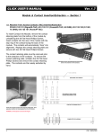
1
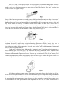
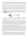
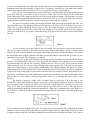
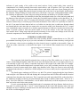
®
Free Guide to Electronics Soldering
By David Kolanowski
Table of Contents
Safety Glasses ________________________________ 2
Solder Tools _________________________________ 2
Solder and Fluxes _____________________________ 4
Typical Solder Joints on PCBs ___________________ 6
6 Hand Soldering Techniques 7 __________________ 7
Trimming Component Leads 10 _________________ 10
ApogeeKits Free Guide to Electronics Soldering
A FREE guide of hand soldering techniques for the beginner level hobbyist or student.
This guide applies to “through-hole” technology hand soldering practices and though most “surface mount”
soldering rules are similar, it does not address some specific intricacies of surface mount soldering practices.
Visit our web site for more FREE educational papers or to check on our latest kit specials.
http://www.ApogeeKits.com/
Many people have never taken the opportunity to pick up a soldering tool and use it to assemble an
electronic project. If you fall into this category, then this paper was written for you, so that the door to the
fascinating world of electronics might be opened a little wider for your education and enjoyment. Many of the
same soldering skills used to assemble electronic projects or kits are also applied to component removal or
making service repairs. Let’s examine the concept of basic soldering techniques used for plated-through-hole
(PTH) electronic component installation, beginning with the most fundamental tools needed to do the job
right.
SAFETY GLASSES
Safety glasses (or at a minimum, your vision correction lenses if you wear any) are your most valuable
yet often forgotten or overlooked tool when performing soldering tasks. After all, it’s hard to solder if you
can’t see. The “smallness” of the job at hand, soldering a component lead to a circuit pad, especially on a
printed circuit board (PCB) crowded with other components that are “in the way”, often requires the person
soldering to get in close to the action in order to see what they’re doing.
Standard solder wire used for electronics assembly and repair have a core of liquid flux, (usually rosin
core) that can rapidly boil under the heat of an applied solder iron, and cause small droplets of flux or hot
molten solder to be propelled off of the work surface and into your eyes! Take it from someone who has
experienced this first hand, this is something you want to avoid. It happens too fast to “dodge the bullet” and is
quite painful. It can ruin your day and enthusiasm for your project, not to mention the potential damage it
could cause to your eye. Find or obtain some protective eyewear and keep it handy in your toolbox for
soldering jobs.
SOLDER TOOLS
There are many types of soldering tools available for purchase on the market, and like most tools there
are some types that are more suitable for a particular job than others. For example, it wouldn’t make sense to
select and use a big bulky soldering iron or a “soldering gun” to perform assembly and repair of electronic
circuit boards containing small electronic components. See Figure 1.
Figure 1
Such irons have a very high thermal mass, usually a large wattage rating and are better suited for an
electrician working with heavy gauge wires or a plumber working on small copper tubing. The amount of heat
generated by such large irons and the inability to keep it focused on a small enough area would quickly make
ribbons out of PCB printed wiring, and burn the circuit pad landings right off of the circuit board. Most
electronic components also have specific ratings of temperature and duration that they can withstand from the
soldering process. This is usually not much of a concern as long as proper component mounting and good
soldering techniques are followed. That’s where a little knowledge, your own soldering skills, and good
practice come into play.
There’s no need for an expensive solder iron to assemble or repair most “through-hole” electronic
assemblies. A “workable” iron can be found for under $10 (US) and might be adequate for the person who
needs to use it only a few times per year for short periods of time. The portable “pencil type” of solder iron
shown in Figure 2 is a typical example.
Many of these have no replacement tips or other parts available and should be considered cheap “throw-away”
irons. They’re often poorly temperature regulated and if used for longer than a few minutes at a time, their
handles can become quite hot and uncomfortable in your hand. This can be an annoyance to say the least, and
may actually add to the difficulty for beginners to learn how to solder. For those who are more active in
electronics, or who don’t mind spending a little more money for better quality, the low end “hobby grade”
irons (also known as solder stations) are a better choice. These will usually do a nicer job just because they’re
easier and more convenient to use than the cheap “throw away” iron. See Figure 3.
Some of these hobby grade solder stations have adjustable temperature setting knobs and better temperature
regulation. Most have a small variety of tip sizes and tip replacements available. Usually, they have an
attached iron holder to hold the hot iron in between uses, and a wet sponge dock, which is used to clean the
iron tip between making solder connections. Prices for these “hobby grade” soldering stations begin around
$20 (US) and average about $40 (US).
For the more professional users, higher quality “commercial grade” brand name soldering stations are
more commonly used. These will have all the features of the hobby grade solder stations, but with better
performance specifications, “grounded” tips for anti-static considerations, more tip sizes and replacement part
options available, and other optional accessories. Expect to pay a minimum of $100 (US) for an entry level
commercial grade soldering station and potentially quite a lot more. Figure 4 shows one typical example of a
commercial grade soldering station intended for everyday use.
Figure 4
All soldering tools have wattage ratings. The wattage is not a major factor of how hot the iron will get,
but is more accurately described as how well the iron can maintain a specific temperature setting while under a
thermal load. Meaning, how much heat the iron can transfer to the area being soldered without falling below
the optimal solder process temperature range. Because they have greater heat capacity, higher wattage tools
can transfer heat to the work pieces without much temperature loss at the tip, so a solder connection can be
made within a shorter period of time. A lot of soldering jobs can be successfully performed using tools within
a wattage power range, keeping in mind that the amount of time and the technique used to create a “good”
solder connection will vary somewhat for tools at opposite ends of that power range. We’ll discuss more
details about technique later, but in the interest of knowing enough to select the best solder tool for a particular
job, it will be helpful to understand the following basic concepts. Ideally as a rule of thumb, a solder
connection or “solder joint” should usually be made within 2 to 3 seconds after the heat of the iron is applied
to the connection. This process forms an inter-metallic compound between the solder itself and the pieces
being joined, (the circuit board pads and the component leads). Applying heat for more than a few seconds
may overheat the solder, causing it to crystallize into a dull, frosty appearing, “cold” solder joint that might
fail sooner rather than later. There are exceptions to the 2 to 3 second rule, such as when soldering large heavy
gauge parts having a high thermal mass. If the heat of an iron is applied to a large connection point for several
seconds, but the solder wire still won’t melt and flow smoothly into the joint, then the iron wattage may be too
low or it may simply require a little more time to do the job. (Proper selection of the solder iron tip plays a role
here). On the other hand, prolonged application of heat, or overheating the solder can not only result in a poor
connection, but can cause damage to the components being soldered or to the conductive traces and pads on
the PCB itself. To select the right solder tool for a job, choose a tool that will allow you to use the lowest
effective temperature setting for making the solder connections within the prescribed time period, without
causing damage to the components and board materials to be soldered. Small, through-hole electronic
components of the type found in ApogeeKits products and other similar PCB assemblies are usually best
soldered with a tool that has a watt rating anywhere between 20 and 50 watts using the right tip selection.
Tip selection: Understanding how to select the proper iron tip for your solder job will aid greatly in
being able to create good solder joints. Generally speaking, the selected solder tool bit should be chisel shaped
at the tip, and the chiseled tip should be about as wide as the connection being made on the board. Thicker,
shorter bits store more heat and provide for more efficient transfer of heat from the tip to the solder joint than
long narrow pointed bits do. See figure 5.
"Tinned" tip area
Figure 5
Except in cases where only the very smallest solder joints need to be made, a long rounded bit pointed
at the tip like a sharp pencil is not recommended because there is less stored heat available at the tip to be
transferred to the joint. If you apply heat and solder to make a joint, but the solder won’t wet the joint within 2
to 3 seconds, then the bit may be too small to do the job optimally. Always select a tip that was designed for
the solder tool you’re using. Never attempt to alter the shape of the tip of a soldering bit by filing on it or by
any other means. Not only is the altered bit not likely to function, but by changing the thermal dynamics of the
bit, you might burn up the heater in your iron and create a working safety hazard.
SOLDER and FLUXES
The most common type of solder used for electronics soldering today is a composition of 63% tin and
37% lead. There is a good reason that this ratio of tin to lead is most commonly used solder formula in
electronics assembly. Consider that the melting temperature of pure tin is 450°F (or 232°C) and the melting
temperature of pure lead is 621°F (or 327°C). When tin and lead are combined in a ratio of about 63/37, this
solder alloy will have a melting temperature of 361°F (or 183°C). It’s interesting that the melting temperature
of the 63/37 tin-lead alloy is lower than the melting temperature of either tin or lead alone, but more
significantly this ratio has the lowest melting temperature of any ratio of tin-lead alloy. This means that by
using this alloy, the soldering process can take place at the lowest possible temperatures, causing the least
amount of stress on the parts to be soldered. But perhaps most significant of all, when tin and lead are
combined in the ratio of 63/37, the alloy exhibits what is known as eutectic properties. Eutectic alloys are
alloys that change instantly from solid to liquid and from liquid to solid at a precise temperature, as opposed to
non-eutectic alloys which will tend to gradually liquefy as their temperature is raised, and slowly thicken back
to a solid as they cool. Because the tin-lead eutectic alloy transitions instantly from a liquid to a solid, it also
produces smooth, bright, shiny, solder joints as there is less of a chance for the joints to be disturbed during
the cooling process. While smooth, bright, shiny joints don’t guarantee a good connection, any different
appearance might provide the assembler a visual signal of other possible problems occurring in the soldering
process.
Non-eutectic alloys are said to pass through a “pasty phase” when they exhibit a plastic state
in-between a liquid and a solid. For this reason, non-eutectic alloys are usually not preferred for electronics
soldering processes. As a non-eutectic alloy cools, its’ state will slowly transition from a liquid to a solid.
During this cooling period, it is subject to disturbances from vibration and uneven cooling. This may result in
a dull, bumpy, frosty or grainy appearing solder joint. While this doesn’t necessarily guarantee that the
resulting connection is bad, such an appearance is normally a visual indication that the integrity of the
inter-metallic bond in the final solder joint may have been compromised, which could result in a high
resistance connection.
Though there are some specific industry or military processes and exotic applications that may call for
using solder alloys of different tin-lead ratios or even “high temp” lead-free solder alloy formulas, currently
none of ApogeeKits’ products fall into these categories. Therefore, ApogeeKits recommends assembling our
kits using basic, tried and true, general-purpose electronics solder wire with a tin to lead ratio of 63% tin to
37% lead (60/40 is fine) as illustrated in Figure 6.
Figure 6 shows a roll of solder wire with a close-up view of the end of the wire. Notice that the solder
wire has a core of flux. The flux core runs continuously through the center of the wire. This is sometimes hard
to see in practice unless the end of the solder wire is melted onto a solder iron tip in such a way as to leave the
core exposed to view.
Like metal alloys, there are different types of fluxes used in electronics assembly soldering processes.
The oldest and most common type still encountered when hand soldering with wire is rosin core (R). Rosin
itself is a natural product collected from trees (Pine trees typically). The rosin is processed and purified to
remove particles, and usually blended with other rosins to produce flux formulas with stable and desirable
characteristics that aid in the soldering process. The primary purpose of any flux is to clean the metal surfaces
of the parts being soldered, so that the solder alloy can adhere and form a strong inter-metallic bond between
the materials. A good solder connection requires the surfaces being soldered to be very clean and free of
natural oxides, oils, or any other contamination. The flux melts and flows out of the solder wire core onto the
PCB pads as heat is applied from the solder iron while making a solder joint.
The flux interacts with all the metal surfaces and the molten solder. It dissolves oxides that would
prevent good solder wetting, and reduces the surface tension of the molten solder alloy, which helps the solder
to flow and feather smoothly and easily onto the metal surfaces it is intended to bond with. Rosin is naturally
and mildly acidic at soldering temperatures only. Once rosin flux cools back down below solder process
temperatures, it reverts back to a solid again. As a solid, rosin flux becomes chemically inert, completely noncorrosive and non-conductive. The sticky residue left behind from rosin flux will eventually dry and form a
protective barrier over the solder joint. Alcohol and other solvents will dissolve rosin it if it needs to be
removed for cosmetic reasons or for application of conformal coatings or the like, but otherwise, removing it
isn’t a requirement.
Another common flux option used in electronics assembly is water soluble organic acid (OA) flux.
Organic acid fluxes are formulated with natural acids like citric, lactic, stearic, and others that are mixed into
solvents like isopropyl alcohol, water, or others. Organic acid flux has some advantages and disadvantages
when compared to rosin flux. Organic acid flux is more corrosive (more active at dissolving oxides) than rosin
flux. Organic acid flux can be easier to solder with in cases were material solderability problems are an issue.
Organic acid flux is water soluble which makes removal of the flux after the soldering process a snap. (Sort
of). Care must be taken when using any flux to not allow it to enter non-sealed components like switches,
sockets, or stranded wire connections. Never use organic acid flux to solder stranded wire. The flux will
“wick” in between the strands of wire and will not be able to be removed. It won’t take long for the organic
acid flux to corrode the wire.
Organic acid flux residue is electrically conductive, and it remains corrosive if left on the assembly.
Therefore, organic acid flux must be removed from the assembly after the soldering process. Don’t worry
about rushing your work while soldering, just don’t let the assembly lay around overnight with organic acid
flux on the board. The OA flux will begin to attack the metal surfaces and if given enough time, will corrode
the assembly. Organic acid flux is easily rinsed off of the assembly with hot running water. Not boiling water,
just hot water. (warm will do).
It’s important to remember that just as care must be taken to avoid getting flux into any unsealed
components of your assembly, it is also true that WATER must be kept out of these same unsealed
components! This can be tricky because BOTH sides of the assembly (top and bottom) should have the
organic acid flux washed off. The assembly must be totally and thoroughly DRY before any electrical power
is applied to the finished circuit assembly. WATER AND ELECTRICITY DO NOT MIX. Water will collect
under components, inside switches, and in other tight places all over your assembly. In a production shop
environment, it’s common for freshly washed circuit assemblies to be blow dried first with compressed air,
(about 30 psi) and then dried in a “cure oven” for about 30 to 60 minutes at about 140°F to 195°F (60°C to
90°C). If you try this at home, be careful that you don’t melt your assembly or start a fire in your kitchen!
Really, it’s NOT a good idea to use your kitchen oven for this purpose. At high temperatures, electronic
assemblies could out-gas by-products that are not suitable for human consumption and you wouldn’t want to
breathe this or allow it a way to get into your food.
For most plated through hole electronics soldering jobs, the author uses and prefers Kester brand
organic acid core solder wire. Formula SN63 PB37 (63% tin and 37% lead) with a .031 diameter, core size 66,
flux type 331. The water soluble flux residue is biodegradable and will rinse off easily with plain warm water.
This eutectic solder wire is available from Mouser Electronics, Digi-Key, and almost any other distributor who
sells Kester solder. I’ve never seen it damage or corrode any assemblies even when they weren’t washed for a
couple of days after soldering. I’ve seen organic acid flux eat pits into stainless steel floors of wave-solder
machines and dissolve aluminum foil into a layer of goo over periods of time though, so I wouldn’t want to
leave it on my assemblies very long. When at home, I wash my assemblies under hot running water in a sink
while I rotate the assembly to carefully avoid getting water inside any open components. Of course, some
water usually ends up where you don’t want any, so I gently blot, blow and shake the clean assembly dry and
blast it with a hot hair dryer until I’m convinced that it’s completely dry inside and out. So far, I’ve had no
problems.
Don’t ignore your own safety and cleanliness! You should avoid breathing solder flux fumes created
from the heat of soldering. In large enough concentrations it can irritate your eyes and lungs. Work in a
ventilated area, or open a window and place a fan near your work area such that the fan can blow the fumes
out the window. Avoid blowing a fan directly on your work cooling your solder tool. Wear safety glasses to
keep boiling flux or flying solder drops out of your eyes. Listen to your mother and wash your hands. Solder
and even the leads of electronic components usually contain some amount of lead. Lead is a soft metal and
trace amounts of it can rub off on what it comes in contact with, and this includes your hands. Wash your
hands with soap and water when you’re finished handling solder wire and tools, especially before handling
food. Avoid having food in your work area or putting anything in your mouth until you clean yourself up.
TYPICAL SOLDER JOINTS ON PCBs
With electronic assemblies implemented on a single sided PCB, the leads of the components are
normally inserted through the component mounting holes from one side of the board (the top) while all the
conductive circuit traces and pads are located on the opposite side of the board, (the bottom). The bottom side
is also known as the “solder side” of the board because after component leads are inserted from the top
“component side”, the assembly is then turned over to perform the soldering work on the bottom side of the
board. Solder is applied to the PCB pads and component leads to form a solder “fillet” on the solder side of the
assembly. Figure 7a illustrates a typical cross-section view of a through-hole component soldered to a “single
sided” PCB.
Figure 7a
Figure 7b
When double sided or multi-layer PCBs are manufactured, the holes are plated through with metal
(plated copper). This is done to provide electrical connections from conductive traces on the bottom side of the
board to conductive traces located on the top of the board, in addition to any internal circuit traces contained
within the laminate of multi-layer boards. When mounting through-hole components to double sided or
multi-layer PCBs, the component leads are usually inserted through the mounting holes from the top side of
the board just as they are on single sided boards. The assembly is then turned over to perform soldering on the
bottom side of the board. Figure 7b illustrates a typical cross-section of a through-hole component soldered to
a double sided (or 2 layer) PCB. Notice that figure 7b also shows “top side fillets”. This solder is not added
from the top component side of the board, but rather, molten solder is flowed through the holes while solder is
applied from the bottom side of the board. It can be seen from figure 7b that when soldering 2 layer or
multi-layer PCBs, an additional amount of solder is required to form a solid fillet all the way through the hole
from the bottom side of the board to the top side of the board.
Improper fillets: Whether the solder process is performed by hand with a solder iron, or by a mass
production wavesolder machine, it occasionally happens that solder does not, or will not flow completely
through a 2 layer or multi-layer PCB hole, and wet the pads on both sides of the board. This is sometimes an
indication of metal plating problems on the inside of the hole because solder will not wet to the inside surface
of non-plated holes. More often than not though, this is caused by a problem with the soldering process itself
and this process, or manual technique, should be adjusted for better results. The assembler should strive to
improve the process or practice the manual soldering technique to obtain optimum results.
If it can be determined that the integrity of the hole plating is sound, and that the soldering process
itself is the cause of poor solder penetration in plated through holes, then sometimes it is best to leave an
improperly formed solder fillet as it is, rather than attempting to rework it. This depends on the reliability
standards that the final assembly must measure up to. For example, medical life support equipment and
military hardware must meet extremely high standards of reliability. Specific standards and criteria exist that
are used to measure what is, and what is not acceptable. For most if not all consumer grade electronics such as
ApogeeKits’ kit products, it is not recommended to re-melt a solder joint to rework or “repair” a solder joint
just for cosmetic reasons. Statistical analysis shows that the additional heat and stress placed on the
components, plus the effect of reheating the inter-metallic bond of the solder joint to a molten state, most often
results in reduced reliability of the solder joint.
HAND SOLDERING TECHNIQUES
In this section we’ll discuss the actual manual technique of creating a good solder joint. Depending on
the different types of solder joints required to build any particular project, it may be that you could find it
difficult or impossible to make all your solder connections with a single solder iron and a single bit. To
simplify things for beginners, a simple “starter kit” type of project should be attempted first, in order that you
should have a chance to practice one size and type of solder joint repetitively and gain some experience before
moving on to more advanced projects. Keep the previous sections in mind as you evaluate the tools you need
for a project. Often, with some simple attention to technique and the subjects already covered in this tutorial,
many projects may be assembled with a single iron and bit. With proper tool selection, all current ApogeeKits
products can easily be assembled with a single solder tool and bit. There’s no substitute for experience though.
Perhaps it’s time to jump in and “get your hands dirty”. If you don’t already have a soldering tool, it’s
suggested that you obtain one and follow along this section with live practice. Or, read on anyway and gain
knowledge. For the remainder of this guide, we’ll refer to your soldering tool as a solder iron. If you have a
solder station, consider the “iron” to be the handle and soldering bit of the tool you’re working with. If you’re
beginning now with a brand new soldering iron, let’s examine a few things before you turn it on and get it hot.
Refer to the user manual of your solder iron for the usual operating instructions and safety precautions. First,
with the iron off and cool to the touch, check that the bit of the iron is mounted securely in the handle. Heat
won’t transfer efficiently from the heater in the handle to the bit, unless the bit is snug and secure in the
handle. That might seem rather obvious, but you may be surprised how often loose solder iron bits cause the
frustration of electronic assemblers.
Next you’ll need a very wet sponge to clean your iron tip with while soldering. If you have an iron
holder and a wet sponge dock, soak the sponge thoroughly with water and place it in the dock for use. If you
don’t have a wet sponge dock, find a small clean sponge and a small dish to keep it soaked with water in. Keep
this handy while you work. (Don’t use any sort of plastic sponge material or synthetic sponge that may melt
when the hot iron touches it). The type of sponge that is compressed (flat) when it’s new and swells up to full
size when it’s wet is the right kind of sponge for this job.
Plug your iron into the power outlet and switch it on. If the temperature of your iron is adjustable, set
the temperature knob or buttons to about 700°F (371°C). Keeping the hot iron over your work table with the
hot tip pointed down, apply some solder wire to the tip of your iron as it begins to heat up. As the tip of the
iron reaches the melting temperature of the solder, melt some solder all over and around the pointed tip of the
bit. This is known as tinning the tip. Refer to the “tinned tip area” note in figure 5. Slowly rotate the hot iron
and try to completely cover the tinned tip area of the bit with solder near the chiseled tip of the bit. Don’t
worry about applying too much solder here. When you have enough solder on the tip, it will begin to drip off
of the tip.
Be careful of where you allow the hot molten solder to drip! This is how you should treat your iron tip
whenever you place it into the holder for storage after each use. Do this whenever you need to leave a hot iron
in the holder for more than a few minutes at a time, and always right before you shut the iron off after each
use. Never let the tip of a hot solder iron sit “dry” of solder for very long. Keeping a heavy coating of solder
on the tip of your iron will protect the tip from oxidation that otherwise could make soldering quite difficult,
and will help maintain good wetting to, and heat transfer from, the tip of your iron to your work. Keeping
plenty of solder on the tip of your solder iron will extend the life of both the tip and the heater element of your
solder iron.
Begin learning your skills with a beginner skill level kit or project following the assembly instructions
carefully. The soldering surfaces of your PCB and the components should be free of dirt, oily fingerprints or
any other contamination that will reduce solderability. Insert a component in the correct location so that all the
leads of the component will pass through the PCB and are accessible to soldering on the bottom side of the
board. Don’t do any trimming or clipping of the lead length yet. This is done after the solder joint is created.
Carefully flip the “assembly” over to expose the bottom “solder side” of the board. If the component on the
top of the board tends to fall out of the holes when the assembly is turned over, you can re-insert the
component and try “clinching” the leads on the bottom side of the board (bend them slightly) to hold the
component in place. Be careful not to bend the leads so much as to cause short circuits to any adjacent
component leads or connections. Slight bends of the leads very close to the pad of the PCB are usually
sufficient to create enough friction with the board to hold the components in place.
Sometimes, for various reasons, bending the leads isn’t desirable. You will undoubtedly discover other
ways to hold components in place. You can use tape, but this sometimes leaves glue behind after it’s removed.
You can place an object between the component and the table top to create a “high spot” under your work that
pushes up on the component when the bottom of the board is facing toward you, but sometimes the “uneven
work surface” this creates is just another problem. There are special tools that address this issue that you could
obtain and use. One such tool is a frame that holds your PCB assembly with the top side facing up while you
install as many components as you like. When you’re ready to turn the assembly over to solder, you clamp on
or close a soft, conformable, anti-static, heat resistant, material over the component bodies to hold them firmly
against the board when the assembly is flipped over for soldering. Such tools are very handy and certainly
make mass production more efficient, but are not very economical for the average hobbyist.
Once you have your component(s) properly held in place with the bottom side of the assembly facing
up for easy soldering, you’re almost ready to create your solder joint. With the tip of your hot solder iron
freshly tinned with solder, gently wipe the tip of the iron over the clean wet sponge. The object here is to allow
the steam and friction generated from this action to clean the tip of the iron. One or two brisk wipes across the
sponge should be sufficient to produce a bright clean silvery iron tip ready for soldering.
The process of creating a solder joint on single sided and multi-layer PCBs is essentially the same. The
only major difference is the amount of solder used to create the joint. First we’ll look at the process to create a
solder joint on a single sided PCB. Refer to figure 8. Place the freshly cleaned tip of your hot solder iron in
contact with both the pad of the PCB and the lead of the component to be soldered. At the same time, bring the
end of your solder wire in very gentle contact with the tip of the iron at the spot where it touches the pad and
the lead.
Figure 8
You first want the flux to melt and flow out of the solder wire core onto the surface of the materials.
This will be quickly followed by the solder melting at this junction and creating a bridge of molten solder
between all of the contacted surfaces. The molten solder bridge will quickly increase the contact area between
the iron and the metal surfaces, and this will further increase the transfer of heat from the tip of the iron into
the surfaces being joined. This all happens very quickly.
As soon as you see the solder starting to melt, begin to gently feed solder wire into the junction until it
produces just enough molten solder to cover the pad all the way around it’s circumference, to create a solder
fillet that envelops the pad and the lead being soldered. Don’t use the tip of your iron to push the molten
solder around the joint. If you have trouble directing solder to the opposite side of the joint, try moving the
solder wire while keeping it in contact with the molten solder. This will help distribute flux where it is needed
and facilitate the flow of the molten solder. When enough solder has been fed to the joint for the formation of
a proper fillet, stop feeding solder wire and remove the end of the wire from the joint area. Keep the hot iron in
the joint for an additional 2 seconds, and then gently pull the hot iron directly out of the molten solder. Don’t
pull the iron out of the solder by lifting up against the lead or by re-directing the molten solder in any
direction.
The process of creating a solder joint on a double sided or multi-layer PCB is the same as just
described for single sided boards and simply requires that a small additional amount of solder be fed into the
joint. On double sided or multi-layer boards, you should feed enough solder wire into the joint so that as it
melts, it will flow down through the hole and out onto the top of the board to create a fillet that wets the
surface pads and lead at both ends of the plated-through hole. While this is sometimes easier to say than it is to
do, all it takes is a little bit of practice and experience to master the skill, and produce consistently good results
every time.
Figure 9 illustrates some finished solder joints. Two of the joints in the illustration were made with the proper
amount of solder, and one of the joints shows the result of feeding a little too much solder wire into the joint.
A properly formed solder fillet will feather smoothly between the surfaces joined by the solder. This is also an
indicator of good wetting of the solder to the metal surfaces. Poorly wetted solder joints caused by
contamination won’t feather smoothly between the metal surfaces, and will produce “ball” type solder joints
similar to the one shown in figure 9 that was made with too much solder. In the case of poor wetting, the joint
produced will have a higher than normal electrical resistance due to the lack of an inter-metallic bond between
the materials. Though feeding too much solder into a joint doesn’t cause poor wetting underneath the solder,
the similarity in appearance to joints with poor wetting means that you should try to avoid this condition.
Just how much solder wire should be fed into the joint depends on the size of the joint being made and
the diameter of the solder wire being used. Creating the joint should require feeding no more than about ¼ to 1
inch of solder wire into the joint. If it requires more than this amount of solder wire to produce a sufficient
amount of molten alloy to create the proper fillet, then the diameter of the solder wire is probably too small for
the job. If you must feed more than an inch or so of solder wire into the joint, it could cause disruptive hand
movements and take more time than you want to take to create the solder joint. Remember the 2 to 3 second
rule. It should take about a second or so to feed the required amount of solder wire into the joint, followed by
about 2 seconds of heat to allow the molten solder to wet to the surfaces in the joint and create the
inter-metallic bond. Taking longer than this prescribed amount of time could cause damage to the PCB, the
electronic components, the inter-metallic bond in the joint, or all three.
TRIMMING COMPONENT LEADS
Excessive lead length on the solder side of the assembly should be trimmed down to size. This will
prevent them from being in your way as you work, and reduce or eliminate the chance that they would get bent
over and create a short circuit to anything else after electrical power is applied to the assembly. Figure 10
shows the solder connections we discussed from figure 9, but with the leads trimmed down to the proper
length.
The component leads should be trimmed down to the top of the fillet with the use of a pair of wire
cutters. Avoid cutting through the solder fillet just to lower the height of the joint. It’s not always necessary or
even advisable to trim every kind of component lead down to the height of the solder fillet. For example,
components like PCB mounted transformers, terminal blocks, power jacks, and other parts that can carry large
amounts of electrical current usually have stubby large diameter leads. Using wire cutters to trim such large
component leads after they’re soldered to a PCB could put a lot of stress on the joint, the component itself, and
the PCB.
The plated copper conductors on PCBs are very thin! The action of cutting through the large diameter
lead could put a side load on the PCB and dislodge the circuit pad from the PCB hole and break the electrical
connection from the pad to the circuit trace. This is especially true with single sided PCBs, as they don’t have
the additional strength provided by the plated-through holes found on double sided boards. Don’t be in a
hurry. Even if the leads are a small diameter, even on double sided boards, avoid the temptation to trim more
than one lead at a time for the same reasons.
If you’re concerned that the finished lead length of a component with large diameter leads may be too
long after it’s soldered, then do a “test fit” of the component on the board, and determine where the lead
should be cut before soldering it onto the board. Trim the leads on these components before they’re soldered to
the PCB to avoid damaging the board.
ApogeeKits hopes that you have found the information in this free tutorial helpful!
ApogeeKits is working on more free tutorials that cover many electronics related subjects. Please
check our website for new tutorials and special deals on ApogeeKits products!
http://www.ApogeeKits.com