1
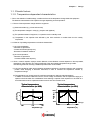
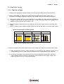
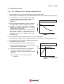
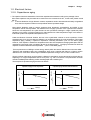
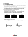
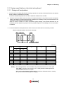
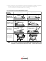
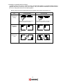
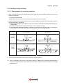
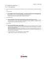
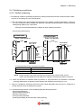
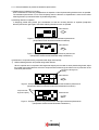
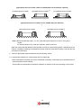
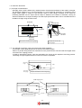
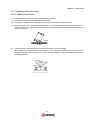
CK-E-1404-01 Date: TO: Safety Application Guide for Multilayer Ceramic Chip Capacitors Signature by receiver(s) Date * Please sign all copies of this document and return one copy for our records. Capacitor Division Kyocera Corporation Prepared by: Checked by: Approved by: This guideline only provides the information for safe and better ways in use of multilayer chip capacitors in order to improve safety of electronic equipment. This guideline shall not assure the product safety of applied electronic components and electronic equipment even when applications comply fully with this guideline. -1- Table of Contents Page Chapter 1 Design 1-1.Climatic factors 1-1-1. Operating temperature P-4 1-1-2. Temperature dependent characteristics P-5 1-1-3. Atmosphere surroundings (gaseous and liquid) P-6 1-1-4. Exposure to irradiation P-7 1-2. Electrical factors 1-2-1. Measurement of capacitance P-8 1-2-2. Applied voltage P-9 1-2-3. Applied voltage and self-heating temperature P - 10 1-2-4. DC voltage and AC voltage characteristics P - 11 1-2-5. Capacitance aging P - 12 1-2-6. Piezo-electric phenomenon P - 13 1-2-7. AC voltage withstanding test P - 14 1-3. Mechanical factors 1-3-1. Vibration and shock P - 15 Chapter 2 Mounting 2-1. Design specifications of printed wiring board 2-1-1. Designs of land pattern P - 16, 17 2-1-2. Placement of the capacitor to printed wiring board P - 18, 19 2-2. Handling of capacitors before mounting 2-2-1. Information before mounting P - 20 2-2-2. Handling of packing P - 21 2-3. Handling during mounting 2-3-1. Maintenance of mounting machine P - 22 2-3-2. Adhesive selection P - 23 -2- 2-4. Soldering conditions 2-4-1. Flux selection P - 24 2-4-2. Flow soldering P - 25, 26 2-4-3. Reflow soldering P - 27 ~ 30 2-4-4. Soldering iron P - 31 2-4-5. Soldering rework using a spot heater P - 32, 33 2-5. Cleaning conditions 2-5-1. Cleaning of printed circuit board P - 34 2-5-2. Cleaning solvent P - 35 2-6. Caution for post mounting 2-6-1. Evaluation of strain in processes P - 36, 37 2-6-2. Printed circuit board cropping P - 38, 39 2-6-3. Mechanical shock P - 40 2-6-4. Electrical test on printed circuit board P - 41 Chapter 3 Caution during operation of equipment P - 42 Chapter 4 Caution during transportation and storage 4-1. Caution during storage P - 43 4-2. Caution during transportation P - 44 P - 45, 46 Chapter 5 Safety standard Chapter 6 Safety and environment 6-1. Abnormal overheating P - 47 6-2. Disposal of capacitors P - 47 Terms and definitions 1. Herein metric size code is expressed with letter “M” following the metric size code. ex.) 1608M for 1608 metric 2. Herein capacitor types are expressed as follows: class 1 : Temperature compensating capacitor (COG, NPO) class 2 : High dielectric constant capacitor (X5R, X7R, Y5V) -3- Chapter 1 Design 1-1. Climatic factors 1-1-1. Operating temperature 1. Upper category temperature (maximum operating temperature) Any operating temperature should not exceed the upper category temperature. It is necessary to select a capacitor whose rated temperature is higher than the operating temperature. Also it is recommended to consider the temperature distribution in equipment and seasonal temperature variable factor. 1-1. Problem due to exceeding the rated temperature range When the capacitor is used at a temperature above the upper category temperature, insulation resistance of the capacitor may deteriorate and cause rapid current increase and a short circuit. 1-1-1. Factors of temperature rise (1) Ambient temperature ① Outside temperature of equipment ② Inside temperature of equipment due to heat accumulation ③ Radiation heat from heating components such as Power transistors, PTC thermistors, etc., around the capacitor. ④ Thermal conduction through the pattern of printed wiring board. 1-2. Problem due to self-heating of the capacitor The surface temperature of the capacitor shall be the upper category temperature (maximum operating temperature) or less, including self-heating. (See Chapter 1-2-3) 1-2-1. Self-heating (1) Due to ESR of capacitor by AC current Special attention to high frequency circuits because of self-heating of the capacitor due to ESR by AC current. (2) Due to ESR of the capacitor by rapid charging/discharging (3) Due to exceeding the rated voltage When using a capacitor in a circuit which causes self-heating, confirm that the surface temperature rise of the capacitor is less than or equal to 20°C, and also that the temperature is at or below the upper category temperature of the capacitor. (See Chapter 1-2-3) 1-3. Consult us before using a capacitor in equipment which requires a very high degree of reliability, such as medical equipment, aerospace applications or nuclear equipment. Malfunctions of medical, space, nuclear (power plant) or other vital equipment may endanger human life or have serious consequences for society. Capacitors to be used in the equipment mentioned above need to be specially designed for obtaining higher reliability than those for general purpose. -4- Chapter 1 Design 1-1. Climatic factors 1-1-2. Temperature dependent characteristics 1. Prior to the selection of suitable ratings, consider the factor of the temperature change inside the equipment. The electrical characteristics of the capacitor changes depending on the temperature. 1-1. Factors of the temperature change within the equipment (1) Seasonal variation (e.g., winter and summer) (2) The temperature changes in a day (e.g., daytime and nighttime) (3) The operational status of equipment, i.e. operation mode or standby mode (4) Temperature in the capacitor rises effected by the heat conduction or radiant heat from the nearby components. 1-2. Influence of operating temperature on electrical characteristics (1) At a high temperature; - Decrease of capacitance - Increase of ESR at high frequency - Decrease of insulation resistance (2) At a low temperature; - Decrease of capacitance - Increase of ESR at low frequency 1-3. Since a ceramic capacitor employs ceramic dielectric, whose dielectric constant depends on the temperature, capacitance of the capacitor may change significantly when the operating temperature range is wide. The following actions for securing a suitable capacitance are recommended. (1) It is recommended to make narrow operation temperature variation by component selection and component position under designing of electronic instrument, in order to minimize the capacitance variation by temperature change. (2) The capacitance may change even if the ambient temperature is within the rated temperature. In addition to the above mentioned concern, the DC voltage characteristic and the capacitance aging of a capacitor should be taken into consideration when selecting a capacitor if the capacitor is to be used for a circuit that needs a narrow capacitance tolerance such as a time constant circuit. Typical temperature characteristics (ex.Y5V) Typical temperature characteristics (ex.X5R) +22% C/C(%) C/C(%) +15% 0 -15% 0 -82% --55 +25 Temperature Chapter 1 -30 - +85 +25 + +85 + Temperature (oC) (oC) -5- Design Chapter 1 Design 1-1. Climatic factors 1-1-3. Atmosphere surroundings (gaseous and liquid) 1. Restrictions of use on operating environmental (climatic) conditions. Confirm the condition of operating environment. If necessary, select an appropriate capacitor or take preventive measures for equipment design. 1-1. Restricted factors of operating environment to capacitors (1) Places directly splashed with water, brine or oil. (2) The place of dew condensation. (3) The place full of corrosive gas (e.g. hydrogen sulfide, 2-oxidization sulfur, chlorine, ammonia, etc.) This includes fumigation for insects or rodents during transportation and storage or maintenance of the equipment also. 1-2. The capacitor used on the above unsuitable operating environment may deteriorate and will not satisfy the required performances. (1) The capacitor splashed with water or brine will be sure to short-circuit. Corrosion of its terminals and permeation of moisture into the inside may shorten the lifetime and may result in failure. (2) The same phenomenon mentioned above may occur when the electrode or terminals of the capacitor are dewed. (3) Deterioration of the characteristics and insulation resistance due to oxidization or corrosion of the terminal electrodes may cause breakdown of the capacitor when it is exposed to corrosive gas or volatile gas of solvent for long time. -6- Chapter 1 Design 1-1. Climatic factors 1-1-4. Exposure to irradiation 1. Restriction against irradiation Confirm the environmental conditions and select an appropriate capacitor. Set up a cover to prevent direct rays of the sun. Please consult us about details. 1-1. Direct energy (1) Direct sunlight (2) Ultraviolet rays (3) X-ray, etc 1-2. Use the capacitor according to the environmental condition specified in the product specifications. Otherwise, the capacitor may deteriorate and not perform as expected. The lifetime of the capacitor may be shortened by a temperature rise in a piece of equipment, when the equipment is subjected to direct sunlight. (See Chapter 1-1-1 and 1-1-2) -7- Chapter 1 Design 1-2. Electrical factors 1-2-1. Measurement of capacitance 1. Measure capacitance with the voltage and the frequency specified in the product specifications. 1-1. Measure the capacitance under the conditions specified in the product specifications. Example of measuring conditions of capacitance Class Rated capacitance Class 1 Class 2 CN 1000pF CN 1000pF CN 10F CN 10F Measuring frequency Measuring voltage V r.m.s. 1 MHz 10% 1 kHz 10% 1 kHz 10% 120Hz 10% 0.5 to 5.0 1.0 0.2 0.5 0.2 Class 1 : Temperature compensating capacitor (COG, NPO) Class 2 : High dielectric constant capacitor (X5R, X7R, Y5V) 2. Some measuring equipment may not be able to apply the required measuring voltage and the measured value will be underestimated, when capacitance is high. Measuring equipment with Auto Level Control (ALC) function is recommended. 2-1. Most of the causes of difference in measured capacitance among each measuring equipment result from difference in actual voltage applied by each measuring equipment even if the same measuring voltage is set up. Since higher capacitance makes smaller impedance in capacitors, it shall not disregard the influence of the voltage drop by voltage divider with the output resistance of measuring equipment. The measuring equipment, which has the function to adjust to the measuring voltage automatically, is recommended for the measurement of a high capacitance capacitor. And, when the measuring equipment without the ALC function is used, it is recommended to check and adjust the measuring voltage by a voltmeter. -8- Chapter 1 Design 1-2. Electrical factors 1-2-2. Applied voltage 1. Voltage which is applied to the capacitor should not exceed the rated voltage given in the specifications. 1-1. Applying overvoltage to a capacitor may cause dielectric breakdown and result in a short circuit. The duration until dielectric breakdown depends on the applied voltage and the ambient temperature. 1-2. When pulse voltage with a very short rising time or AC voltage of a high frequency is applied to capacitors, even though the voltage is less than or equal to the rated voltage, the reliability of the capacitor may be influenced. (See Chapter 1-2-3) 1-3. When AC voltage is superimposed on DC voltage, the zero-to-peak voltage shall not exceed the rated voltage. When AC voltage or pulse voltage is applied, the peak-to-peak voltage shall not exceed the rated voltage. Typical voltage applied to the DC capacitor DC voltage E DC + AC voltage E 0 AC voltage E Pulse voltage 0 E 0 0 NOTE Maximum possibly applied voltage. 1-4. Abnormal voltage (surge voltage, static electricity, pulse voltage, etc.) shall not exceed the rated voltage. (1) When capacitors are used in a series connection, it is necessary to add a balancing circuit such as voltage dividing resistors in order to avoid an imbalance in the voltage applied to each capacitor. (2) Concerning overvoltage on AC capacitors (Electromagnetic interference suppression capacitors) These capacitors shall be selected in consideration of the possibility that the supply voltage of the system may rise by up to 10 % of its nominal voltage. -9- Chapter 1 Design 1-2. Electrical factors 1-2-3. Applied voltage and self-heating temperature 1. Confirm whether AC voltage and pulse voltage are continuously applied to the capacitor. Be sure to take into account self-heating when using DC capacitors for AC or pulse circuits. 1-1. General capacitors are designed for DC use. When they are used in a circuit where AC or pulse voltage is applied, the current value may increase and the capacitors may short-circuited due to self-heating. (1) For capacitors of Class 2, it is necessary to maintain the surface temperature shall not increase more than 20°C. (2) For capacitors of Class 1, since the permitted temperature rise depends on the dielectric material, consult us about the details. Note: Class 1 : Temperature compensating capacitor (COG, NPO) Class 2 : High dielectric constant capacitor (X5R, X7R, Y5V) 1-2. When pulse voltage with very short rising time or AC voltage with a high frequency is applied to a capacitors, even within the rated voltage the reliability of the capacitor may be influenced. 1-3. When pulse voltage or AC voltage is applied to capacitors, even within the rated voltage, the capacitor may generate heat due to the current. This self-heating is mainly generated in the dielectric by its dissipation or at the junction between electrodes and dielectric. The self-heating or the current induced by the heat causes the deterioration of insulation and/or damage to the electrodes. If a current which causes self-heating is below the specified value, the capacitor deteriorates very little. However, if a large current causes a high temperature exceeding the specified value, the deterioration of the capacitor may be accelerated and cause a burnout. 1-4. Self-heating of a capacitor depends on the dielectric material, the capacitance, the applied voltage, the frequency, the voltage waveforms and others factors. Moreover, the surface temperature may be affected by heat radiation related to the style of the capacitor, the mounting method to the equipment and the ambient temperature. Since self-heating affects the characteristics of capacitors when ambient temperature changes, even under the same voltage conditions, perform the confirmation of self-heating at room temperature (25 °C). Generally, the correlation of the frequency and voltage, which can be applied to the capacitor, is restricted by peak-to-peak voltage in the low frequency bands, and is restricted by self-heating in the high frequency bands. (See the following figure) Since circuits used in the field have various kinds of voltage waveforms, it is difficult to prepare such data considering all conditions. Consult the component manufacturers or confirm actual self-heating in the equipment. Permitted voltage Peak-to-peak voltage or Zero-to-peak voltage Regulation by self-heating Difference of self-heating by capacitance Frequency -10- Chapter 1 Design 1-2. Electrical factors 1-2-4. DC voltage and AC voltage characteristics 1. The capacitance of a capacitor changes depending on the DC voltage applied. Select a capacitor considering the DC voltage characteristics of the DC circuit in which the capacitor is used. 1-1. The capacitance of ceramic capacitors might change sharply depending on the applied voltage. (See figure) Confirm the followings in order to ensure desired capacitance. C/C(%) (1) Confirm whether the capacitance change according to the applied voltage is within an allowable range or not. (2) Regarding DC voltage characteristics, capacitance decreases as voltage increases, even if the applied voltage is below the rated voltage. Therefore, when a capacitor is used in a circuit with a narrow range of capacitance change allowance like a time constant circuit, it is recommended that the capacitance is within the allowable range under operating voltage. DC voltage characteristics 0 0 DC voltage (V) 2. The capacitance of capacitor changes depending on the AC voltage applied. Select a capacitor considering the AC voltage characteristics of the AC circuit in which the capacitor is used. (1) Confirm the capacitance change according to the applied voltage is within an allowable range. (2) Confirm the measuring conditions of the capacitance specified in the catalogs or product specifications. Capacitance during use may differ from the nominal capacitance. Note: See Chapter 1-2-1 for the measurement of capacitance. ΔC/C(%) 2-1. The capacitance of ceramic capacitors might change depending on the applied voltage. (See figure) Confirm the followings in order to secure the capacitance AC voltage characteristics 0 1.0 AC voltage(V.r.m.s.) -11- Chapter 1 Design 1-2. Electrical factors 1-2-5. Capacitance aging 1. The capacitor has the characteristics of which the capacitance decreases according to the passage of time. Since these capacitors may be unable to be used for the time constant circuit etc., for that case, please consult with us. 1-1. In ceramic dielectrics of high dielectric constant, capacitance tends to decrease almost linearly to logarithmic time, when the capacitor is left at room temperature without impressed voltage. Most ceramic dielectrics used for ceramic capacitors have ferroelectric characteristics, and exhibit a curie temperature. Above this temperature, the dielectrics have a highly symmetric cubic crystal structure whereas below the curie temperature, the crystal structure is less symmetrical. Although in single crystals this phase transition is very sharp, in practical ceramics it is often spread over a finite temperature range. In all cases it is linked with a peak in the capacitance/temperature curve. Under the influence of thermal vibration, the ions in the crystal lattice continue to move to positions of lower potential energy for a long time after the dielectric has cooled down below the curie temperature. This makes capacitance aging, whereby a capacitor’s capacitance continually decreases. (Line A in the below graph) However, if the capacitor is heated to a temperature above the curie temperature, de-aging takes place and the capacitance lost through aging is regained. (B point in the below graph) The aging recommences when the capacitor cools down below its curie temperature. (Line C in the below graph) This is a phenomenon of shifting to a lower energy state by which the ceramic dielectric becomes more stable. Therefore, take capacitance aging into consideration when using a capacitor with Class 2 or Class 3 ceramic dielectrics for a circuit with a narrow range of allowable capacitance change, such as a time constant circuit. Since the effects of this aging can be reversed, a dielectric's capacitance can be returned to its original value by subjecting it to a higher temperature than its Curie point, e.g. 125°C for BaTiO3. The phenomena can been noticed immediately after soldering or after reworking/repair with a soldering iron. The examples of capacitance aging are shown as follows. Capacitance aging of before-and-after heat treatment C/C(%) C/C(%) Capacitance aging at room temperature 0 A log t Time (h) B 0 C Heat treatment log t Time (h) -12- Chapter 1 Design 1-2. Electrical factors 1-2-6. Piezo-electric phenomenon 1. Some capacitors (Class 2) show piezo-electric phenomenon which transforms electric energy into machine energy, and vice versa. 1-1. Effect of size of capacitor When a signal of a certain specific frequency is applied to a capacitor, the capacitor resonates at the character frequency decided by the size of capacitor, and may generate a noise. 1-2. Effect of mechanical shock When a mechanical vibration or shock is applied to a capacitor, the mechanical energy is changed into an electrical signal and the capacitor may generate a noise. (Caution is particularly required for use near an amplifier part.) As a practical measure, changing the dielectric material used in a capacitor to a low loss material not subject to the piezo-electric phenomenon is effective. Changing to the temperature compensating capacitor (Class 1) is also effective. 1-3. Effect to the performance and reliability Although the phenomenon may cause no problem on the component performance and reliability, the roar of the capacitor may worry some users. Since this may result in generating of a noise, confirm generating of a noise in actual equipment operation. 2. As a practical measure, it is effective to replace the capacitor with one whose structure, size and characteristics differ from those as shown above 1-1 and 1-2. It is effective to change the dielectric material of the capacitor to a low loss material which is not affected by the piezo-electric phenomenon, or changing to a Class 1 capacitor. As for other methods, in order to suppress resonance with the steel case of a printed circuit board, changing the mounting direction of the capacitor or affixing the capacitor to the steel case of the printed circuit board with adhesives may also be effective. -13- Chapter 1 Design 1-2. Electrical factors 1-2-7. AC voltage withstanding test 1. Confirm test conditions (voltage, time and waveform) of AC voltage withstanding tests for capacitors for electromagnetic interference suppression use in the primary circuits. 1-1. Confirm that the test conditions (voltage, time and waveform) of the AC voltage withstanding tests at the incoming inspection and/or assembly process are within the specified conditions. Failure of withstanding voltage may occur when applied voltage or time exceeds the specified conditions. 1-2. Confirm a specified voltage wave form for the AC voltage withstanding test. When the voltage wave form is a sine wave, any peak voltage which is more than 2 times of specified effective voltage shall not be applied to the capacitor. The applied voltage wave form may be distorted by the dielectric material of the capacitor or the withstanding voltage test equipment, so that it may exceed 2 times the specified effective voltage. Distorted wave forms of a sine wave with a voltage of 1000 V rms are shown as follows. Example of sine waveform (1414V.0-P) Example 1 of distortion waveform (2000V.0-P) Example 2 of distortion waveform (2800V.0-P) 1-3. For the AC voltage withstanding test, apply a specified voltage using a zero crossing start after the capacitor's terminals are connected securely to the test equipment. When a spark discharge is generated by a poor connection with test equipment, or by applying voltage with test equipment which does not employ a zero crossing start, abnormal voltage higher than the specified voltage may be generated. Zero cross start Not zero cross start Abnormal voltage on on -14- Chapter 1 Design 1-3. Mechanical factors 1-3-1. Vibration and shock 1. The limits of mechanical stress (e.g. vibration, shock) in an environment for use of capacitors are specified. 1-1. When vibration and/or shock exceed the conditions specified in the catalogs or product specifications, consult the component manufacturers on their conditions. Take the measures of fixing the capacitor etc. by the equipment manufacturer, if necessary. Since the body of a capacitor consists of ceramic, if a mechanical shock is applied directly, the capacitor may be damaged and a crack may be generated. 1-2. Under the following status, the vibration and/or shock may be applied to a capacitor. (1) During equipment transportation on a rough road. (2) When handling at carrying in or taking out. (3) In a storm during sea transportation. (4) At the launch and landing of a rocket. 1-3. The capacitors that have fallen shall not be used. The quality of these capacitors have already spoiled in many cases. -15- Chapter 2 Mounting 2-1. Design specifications of printed wiring board 2-1-1. Designs of land pattern 1. Since the amount of solder (fillet size) for mounting a capacitor on a printed circuit board influences the capacitor directly, sufficient consideration is necessary. Confirm the suitable land pattern size in order to decide the suitable amount of solder. 1-1. When the amount of solder is too much, stress on a capacitor increases. It may cause a crack in the capacitor. When a land design of a printed wiring board is considered, it is necessary to set up the form and size of the land pattern so that the amount of solder is suitable. When the amount of solder is too little, the adhesion (shear) strength of the terminal electrode may be insufficient, and the capacitor may drop off from the printed wiring board. The reliability of the circuit may also be affected. 1-1-1. Recommendation for land pattern size to which the amount of solder does not excessively increase [Recommended land pattern size of each case size] Chip capacitor Land c b a Solder resist (Unit: mm) Code SIZE a b c 01005 0.13 ~ 0.20 0.12 ~ 0.18 0.20 ~ 0.23 0201 0.20 ~ 0.30 0.25 ~ 0.35 0.30 ~ 0.40 JIS EIA 02 0402M 03 0603M 05 1005M 0402 0.30 ~ 0.50 0.35 ~ 0.45 0.40 ~ 0.60 105 1608M 0603 0.70 ~ 1.00 0.80 ~ 1.00 0.60 ~ 0.80 21 2012M 0805 1.00 ~ 1.30 1.00 ~ 1.20 0.80 ~ 1.10 316 3216M 1206 2.10 ~ 2.50 1.10 ~ 1.30 1.00 ~ 1.30 32 3225M 1210 2.10 ~ 2.50 1.10 ~ 1.30 1.90 ~ 2.30 42 4520M 1808 2.50 ~ 3.20(1) 1.80 ~ 2.30 1.50 ~ 1.80 43 55 4532M 5750M 1812 1 2.50 ~ 3.20( ) 1.80 ~ 2.30 2.60 ~ 3.00 2220 4.20 ~ 4.70 2.00 ~ 2.50 4.20 ~ 4.70 NOTE(1) The creepage distance of basic insulation may be required to be 2.5 mm or more. (See JIS C 6950-1) Therefore, the dimension of “a” for safety standard certified capacitors is recommended to be 3.0 mm to 3.5 mm. When using a safety standard certified capacitor, consider a slit between lands or cleaning, etc. to prevent electrical discharge from creepage. -16- 1-2. When mounting two or more capacitors are mounted on the common land, it is necessary to separate the land with the solder resist strike so that it may become the exclusive land of each capacitor. Unrecommended and recommended examples shown as following. 1-2-1. Recommended and unrecommended examples of soldering Mounting characteristic Unrecommended Recommended Leads of leaded Solder resist component Mounting with leaded component Chassis Mounting on the vicinity of chassis. Chassis Solder (For grounding) Lead of com ponent soldered in later process Wire soldering after mounting Soldering iron Land pattern Excessive solder Solder resist Solder resist Solder resist Common solder land with other chip capacitors(2) NOTE(2) When a capacitor is mounted on a common solder land with another SMD, design the solder resist pattern so that the effective land pattern for the capacitor is exclusive and does not have excess solder. -17- Chapter 2 Mounting 2-1. Design specifications of printed wiring board 2-1-2. Placement of the capacitor to printed wiring board 1. After soldering a capacitor on a printed wiring board, if it is bent during board cutting, board cropping,boardchecking, component mounting, mounting to a steel case, flow soldering of the back of the board after reflow soldering, or handling, a crack may occur in the capacitor. Confirm the mounting position and direction that minimizes the stress imposed on the capacitor during flexing or bending the printed wiring board. 1-1. Recommended mounting arrangement and direction that minimizes the stress imposed on the capacitor during flexing or bending of the printed circuit board is shown as following. Condition Unrecommended Recommended Bending or flexing (Mount capacitor traverses to the direction of stress.) 1-2. Since mechanical stress depends on the position and direction in which the capacitor is mounted near the cutting line, please refer to the following figure. A: Beside perforation (perpendicular to the cut line) B: Beside perforations (parallel to the cut line) C: Beside the slit D: Push-back (perpendicular to the cut line) E: Push-back (parallel to the cut line) E D Perforation C A Stress magnitude: AB>E A>D>E A>C B Slit 1-3. When dividing the printed wiring boards, the intensities of mechanical stress applied to capacitors are different by each dividing method is in the order of: Push-back < Slit < V-groove < Perforation. Therefore, consider not only position of capacitors, but also way of dividing the printed wiring board. -18- 2. Separation of multiple printed circuit board A multiple printed circuit board is divided into each unit board after soldering. If excessive bending stress is applied to the board, a crack may occur in the capacitor. Carry out sufficient consideration for stress control at the time of cutting with reference to the following figures. Bending stress and recommended placement of capacitor when printed circuit board is cut. Point Unrecommended Recommended Direction of bending Bending force is applied to the side on which the capacitor is mounted. Bending force is applied to the side on which the capacitor is not mounted. Capacitor is mounted perpendicular to the slit. Capacitor is mounted parallel to the slit. Capacitor is mounted close to the slit. Capacitor is mounted farther from the slit. Orientation of capacitor Distance from a slit -19- Chapter 2 Mounting 2-2. Handling of capacitors before mounting 2-2-1. Information before mounting 1. The capacitors that were removed from the equipment should not be reused. Since capacitors that were once used may have been influenced by thermal and/or electrical stress, their lifetime cannot be estimated. 2. Confirm capacitance characteristics under actual applied voltage Capacitors consist of dielectric ceramics with voltage dependency. The capacitance may change largely depending on an applied voltage, so confirm the following items: (1) Capacitance change under the applied voltage. (2) Circuit design which the capacitance change does not affect. (3) Measuring conditions specified in the catalogs or product specifications ( Chapter 1-2-1 and 1-2-4). 3. Confirm whether excessive mechanical stress is not added to capacitors by process and/or equipment. The capacitor that was fallen should not be used because it may be electrically and/or mechanically damaged and have a high risk of failure. 4. Confirm capacitance value, rated voltage and other electrical characteristics before assembly. Capacitors may not fulfill the specified performance when used improperly in regards to ratings or characteristics. 5. Prior to use, confirm the solderability of capacitors that were stored for a long time. The capacitors should be used within 6 months. (See Chapter 1-2-5) 6. Prior to measuring capacitance, carry out a heat treatment for High Dielectric Constant capacitors that were in long-term storage. Capacitance aging should be considered in equipment circuit design when using capacitors. Decreased capacitance due to aging of dielectric ceramics can be returned to its initial value by a heat treatment. (See Chapter 1-2-5) -20- Chapter 2 Mounting 2-2. Handling of capacitors before mounting 2-2-2. Handling of packing 1. Store the packed capacitors according to the specified storage environment and term. 1-1. The storage environment and term affects the properties of packaging materials used during storage. The deterioration of the packaging performance due to storage in high temperature and high humidity environments and/or long-term storage may lead to falling capacitors from the package during transport or errors during mounting. ( See Chapter 4-1) 2. The specified packaging is designed to ensure a suitable quality for inserting and mounting. When the capacitors for taping are used for bulk case, the deterioration of capacitor performance, the inefficient of mount operation and the trouble of the machine may occur. The accuracy of dimensions for the taping capacitor is not severer than that of the capacitor for bulk case. 3. Considerations regarding handling of bulk cases 3-1. A case which contains capacitors should be avoided from a shock as much as possible. The shock can lead to chipping, cracking or other damage. 3-2. Unused bulk feeders in production Bulk feeders, which are not used for current production, should not be left on the feeder table. Capacitors in the feeder may be shaken intensively by the movement of the feeder table, and the discoloration of capacitors (Blackening) may be hastened and the solderability may be deteriorated. 3-3. Quantity of SMD per a supply If an excessive amount of capacitors are added to the hopper they may be exposed to excess rubbing due to the vertical movement of the hopper for alignment, which may cause quality deterioration such as poor solderability, cracks and chipping of capacitors. Supply SMDs to standard bulk cases (EIAJ ET-7201A) with one case at a time. 3-4. Remaining SMDs in bulk feeder If capacitors remain in a bulk feeder, they become mixed with the next new lot. In cases where the feeder system does not use up all capacitors, confirm that no capacitors remain in the storage compartment. If a new lot is supplied while capacitors from the previous lot remain in the storage compartment of a bulk feeder, and the adding supply accumulates the damage on the leftover parts, the quality of the capacitors deteriorate. 3-5. Dirt and grime on bulk feeder Check the dirt on the carrier pathway of the components in bulk feeder. The dirt on the carrier pathway causes the supply errors and reduces the operating rate of mounting machine. Moreover, it may cause the failure of the bulk feeder itself. 4. Standards relating to Bulk Cases EIAJ ET-7201A, Reusable bulk case for surface mounting devices -21- Chapter 2 Mounting 2-3. Handling during mounting 2-3-1. Maintenance of mounting machine 1 . When a capacitor is mounted on a printed wiring board, make sure that the following excessive forces are not added to the capacitor. (1) Pressure of sticking nozzle (2) Mechanical shock and stress due to positioning for displacement part of capacitor 1-1. When an sticking nozzle's lowest position is too low, stress is applied to capacitors and cause cracks. Take into account the following precautions: (1) Adjust the lowest position of the sticking nozzle to the surface of the printed wiring board after flattening the board bending. (2) Adjust the nozzle pressure to within a static load of 1 N to 3 N during mounting. (3) On double-sided printed wiring boards, to minimize the impact from the mounting head, it is important to provide support on the bottom side of the printed wiring board. See the following examples. Unrecommended Single sided mounting Recommended Crack Support pin A support pin is not to be underneath Double sided mounting Peeled solder Crack Support pin 2. Perform periodic maintenance and regular checks of the mounting machine. 2-1. When a centering jaw is worn-out, it may cause a crack in a capacitor due to abnormal mechanical impact. Control the closing dimension of the centering jaw and perform sufficient preventive maintenance and timely replacement of it. -22- Chapter 2 Mounting 2-3.Handling during mounting 2-3-2. Adhesive selection 1. When using adhesives before soldering the capacitors to the printed wiring board, confirm the application conditions or consult component manufacturers. Capacitor performance may deteriorate if land pattern size, type or amount of adhesive, curing temperature, curing time, etc. is unsuitable. 1-1. Certain types of adhesive may deteriorate the insulation resistance. Differences in coefficients of thermal expansion (CTE) between the adhesive and capacitors may cause cracks in the capacitors. If adhesive amount, curing temperature and/or curing time are insufficient, capacitors may be misaligned or fall off during handling or soldering. When adhesive amount is excessive, adhesive that overflows to the land area may cause poor soldering, conductivity, curing and/or alignment. If curing temperature and/or time is excessive, capacitor termination and board land surfaces might oxidize so much that adhesion strength and solderability of capacitors may deteriorate. 1-1-1. Selection of suitable adhesive Consider the following requirements when selecting adhesives. 1) Sufficient adhesion strength is needed so that components will not fall or become misaligned in the process of mounting. 2) Adhesion strength shall not deteriorate when subjected to the high heat of soldering 3) Good deispensability and thixotropy 4) Long shelf life 5) Rapid curing 6) Non-corrosive 7) Sufficient nonconductivity 8) Non-toxic 9) Non-halogen compound 1-1-2. The following drawings show optimum amount and shape for adhesive application. Recommended conditions Symbol Example of 2012M/3216M (0805/1206) a Minimum 0.2mm b 70μm to 100μm c No contact with land pattern Dispensed adhesive a a After mounting capacitor b c -23- c Chapter 2 Mounting 2-4. Soldering conditions 2-4-1. Flux selection 1. Flux can seriously affect the performance of capacitors. Confirm the following items to select the appropriate flux. 1-1. Amount of flux 1-1-1. Put the suitable minimum amount of flux uniformly on the printed wiring board when a capacitor is soldered. Flux is applied in order to improve solderability. If the amount of flux is too much, solderability may deteriorate due to too much flux gas being generated during flow soldering. Foaming method is recommended in order to limit the amount of flux. 1-2. Chlorine content 1-2-1. Strong acidic flux should not be used. Use flux that has a chlorine content of 0.1 wt % or less. Flux with excessive amounts of halogen compounds and/or strongly acidic additives for activation may lead to a large amount of residue after soldering, deterioration of surface insulation of capacitors and the corrosion of terminal electrodes or lead wires may occur. 1-3.Type of flux 1-3-1. When using water-soluble fluxes, clean thoroughly. If rinsing is not sufficient, residues of water-soluble flux dissolve easily when exposed to moisture so in high humidity conditions, insulation resistance may deteriorate insulation resistance and reliability by residue that adheres to the capacitor surface. When using water-soluble flux, confirm that capabilities of the cleaning method and cleaning machine are well maintained. Sufficient rinsing and drying are needed to avoid an ion migration in the gap between the printed circuit board and capacitor. 2. Sn-Zn type solder may cause negative effect to capacitor reliability. Please contact us in advance of using Sn-Zn type solder. -24- Chapter 2 Mounting 2-4. Soldering conditions 2-4-2. Flow soldering 1. The soldering conditions (preheating temperature, soldering temperature and their durations) shall be within the limits in the catalogs or product specifications. Perform soldering within these specifications. 1-1. When the capacitors are used exceeding the limits given in the catalogs or product specifications, cracks may occur in the capacitors and the reliability may deteriorate, especially the rapid temperature changes and partial heating during soldering may cause cracks. The temperature profile should be in accordance with the catalogs or product specifications. Generally recommended temperature conditions for flow soldering is as follows: [Recommended flow soldering] For eutectic solder For lead free solder Solder : Sn-3.0Ag-0.5Cu Solder : Sn63 or 60 and Pb 300 Preheat ΔT 150 100 Cool at normal room temperature 50 Temperature ( ゜C ) Temperature ( ゜C ) Peak Temperature 245゜C~260゜C 250 250 200 Preheat 300 Peak Temperature 230゜C~260゜C ΔT 200 150 100 50 0 0 60 to 120sec. 60 to 120sec. 5sec.Max. 5sec.Max. ∆T: Rapid temperature change on the surface of capacitor NOTE Lead-free solder has a higher liquid phase temperature than eutectic solder (Sn-Pb). Confirm the heat resistance of the capacitor in regards to soldering temperature in advance. size Allowed temperature range 1608M(0603),2012M(0805) 3216M(1206) ∆T≦150°C Capacitors larger than 3216M(1206) and smaller than 1005M(0402) are unsuitable for flow soldering. 1-2. When the capacitors are soldered under long duration or high temperature, the dissolution of electrode (leaching), deterioration of adhesion (shear strength) and capacitance decrease may occur. . Example of the dissolution of electrode (leaching) Terminal electrode -25- 2. Proper amount of solder is required. Excess solder generates high contraction stress. The capacitor may also be exposed to thermal and/or mechanical stress resulting in cracks or breaks. Insufficient solder results in deficient capacitor adherence to the printed wiring board, which may cause capacitor detachment or deficient electric connection and reliability deterioration of the circuit may occurs. Typical amount of solder are shown as follows. 【 Solder amount for flow soldering 】 (a) Excess amount of solder (b) Suitable amount of solder Adhesive 3. Caution of flow soldering comparing to reflow soldering 3-1. Flow soldering shall not be applied to the capacitor designed for reflow soldering only. Cracks due to thermal stress or dissolution of electrodes (leaching) may occur and may result in deterioration of adhesion (shear strength) or decrease in capacitance. 3-2. Some large size and small size capacitors are unsuitable for flow soldering. Consult us for details. -26- Chapter 2 Mounting 2-4. Soldering conditions 2-4-3. Reflow soldering 1. The soldering conditions (preheating temperature, soldering temperature and their durations) shall be within the limits in the catalogs or product specifications. 1-1. When the capacitors are used exceeding the limits given in the catalogs or product specifications, cracks may occur in the capacitors and the reliability may deteriorate, especially the rapid temperature changes and partial heating during soldering may cause cracks. Generally recommended temperature conditions for reflow soldering is as follows: [Recommended reflow soldering] For eutectic solder For lead free solder Solder : Sn63 or 60 and Pb Preheat 300 300 Peak Temperature 225 ゜C~ 235 ゜C Peak Temperature 150 100 Cool at normal room temperature 50 ( ゜C ) Higher than 180 ゜C ΔT 200 Preheat 250 Temperature ( ゜C ) 250 Temperature Solder : Sn-3.0Ag -0.5Cu 200 245 ゜C ~ 255 ゜C ΔT Higher than 220 ゜C 150 100 50 0 0 60sec. 60sec. 15sec. Max. 60 to 120sec. 40sec.Max. 5 to10sec. Max. 90sec.Max. ∆T: Rapid temperature change on the surface of capacitor size 3216M(1206) and smaller Allowed temperature range ∆T≦150°C 3225M(1210) and larger ∆T≦130°C NOTE Lead-free solder has a higher liquid phase temperature than eutectic solder (Sn-Pb). Confirm the heat resistance of the capacitor in regards to soldering temperature in advance. 1-2. When the capacitors are soldered under long duration or high temperature, the dissolution of electrode (leaching), deterioration of adhesion (shear strength) and capacitance decrease may occur. 2. Take into consideration tombstone phenomenon (also called "Manhattan phenomenon") for 3216M size or smaller capacitors when the soldering is not proper. . 2-1. The tombstone phenomenon can be avoided by taking the following measures: - reducing land dimensions - applying adequate preheating - optimizing solder amount - ensuring accurate placement - providing equal heating to both terminations during soldering -27- 2-1-1. Recommendations to prevent the tombstone phenomenon 1) Displacement of capacitor in mounting Give consideration to minimizing a displacement of capacitor on land of printed wiring board as much as possible. The tombstone phenomenon occurs more frequently when the direction of displacement is same as the reflow soldering direction (movement direction of printed wiring board). 2) Mounting direction of capacitor In designing printed wiring board, give consideration so that the mounting direction of capacitor (lengthwise direction) becomes a right angle to the reflow soldering direction as much as possible. Reflow direction Figure 1 - Example of placement with lower tombstone phenomenon (Temperature of both terminal electrodes is balanced) Reflow direction Figure 2 - Example of placement with higher tombstone phenomenon (Temperature of both terminal electrodes easily is imbalance.) 3) Placement of a capacitor among components with larger heat capacity ① Reflow soldering direction and printed wiring board direction When a capacitor and a component with larger heat capacity are mounted on same printed wiring board, adjust the printed wiring board direction so that the component flows first through the reflow oven for prevention of the tombstone phenomenon. Component with large heat capacity Reflow direction Figure 3 - Example of printed wiring board direction with lower tombstone phenomenon (Temperature difference between both terminal electrodes is reduced.) Component with large heat capacity Reflow direction Figure 4 - Example of printed wiring board direction with higher tombstone phenomenon (Temperature of both terminal electrodes is imbalance.) -28- ② Distance between a capacitor and a component with larger heat capacity To reduce the risk of tombstoning, design land patterns placing large heat capacity components in such a way that does not subject capacitors to different temperatures. Confirm by checking the surface temperature of the board. Unrecommended Component with large heat capacity Recommended Figure 5 - Distance between a capacitor and a component with larger heat capacity ③ Placement of a capacitor with a component of larger heat capacity The tombstone phenomenon can be suppressed by placing the capacitors in proximity with the side of components with large heat capacity. At this time, too, place the capacitors as close as possible to the components with large heat capacity and make sure that the capacitor is vertical against reflow soldering direction. Components with large heat capacity Reflow direction Figure 6 - Example of placement with lower tombstone phenomenon (Temperature difference between both terminal electrodes is reduced.) Components with large heat capacity Reflow direction Figure 7 - Example of placement with higher tombstone phenomenon (Temperature of both terminal electrodes is imbalance.) 4) Pad dimension Design the pad dimensions so that the land area is as small as possible in order to uniform the solder amount on each land. 3. Mount the capacitor as soon as possible after applying solder paste. 3-1. If the interval between applying solder paste and mounting a capacitor is too long, solderability may decrease due to drying and hardening of the solder paste. 4. Use a suitable amount of solder to form a proper fillet shape. 4-1. Excess solder generates high contraction stress and thermal stress. As a result, cracking or breaking of the capacitor may occur. Insufficient solder results in deficient capacitor adherence to the printed wiring board, which may cause capacitor dropout or poor electrical connection which, in turn, may cause reliability to deteriorate. Typical shapes of solder fillet are shown as follows -29- [Appropriate amount of solder solder for 3216M (1206) size and smaller capacitor] (a) Excess amount of solder 1 (b) Suitable amount of solder ( ) (c) Insufficient amount of solder [Appropriate amount of solder for over 3216M (1206) size capacitor] ] (e) Suitable amount of solder (1) (d) Excess amount of solder Note (1) Recommended fillet height: 1/3~2/3 of the thickness of capacitor or 0.5 mm, whichever is smaller. For the fillet height of very small size capacitors, please consult us. When the components with different case sizes are mounted on a printed wiring board, a suitable amount of solder is controlled considering the land pattern and the mask size (area and thickness), other than the size and height of components. 5. Select an appropriate solder material referring the following notices. 5-1. Inappropriate materials can cause troubles such as solder balls. ・When solder balls are created, remove any solder balls completely. Solder balls may cause deterioration of electrical property and/or reliability. ・Sn-Zn solder may deteriorate the insulation resistance of capacitor under some operating environments. -30- Chapter 2 Mounting 2-4. Soldering conditions 2-4-4. Soldering iron 1. The soldering conditions shall be within the limits in the catalogs or product specifications. 1-1. When soldering capacitors beyond limits of the conditions stated in the catalogs or product specifications, cracks in the capacitor may occur due to thermal stress. Cracks may cause the deterioration of insulation resistance, reliability, and bending strength of the capacitor. When using a lead-free solder which has a high liquid phase temperature (over 200 C), take account of cracks compared to using Sn-Pb eutectic solder. Particularly, partial heating and rapid heating/cooling to a capacitor significantly increases the risk of cracking. The tip of soldering iron should not touch directly to the termination electrodes of a capacitor. Consult us about the conditions not given in the catalogue or equipment specifications. Preferred method Soldering iron Soldering iron Not good Good 2. Set soldering condition in order to reduce thermal stress to the capacitor prior to soldering. 2-1. Preheating When the temperature difference between the tip of solder iron and the capacitor or the printed wiring board is large, a crack may occur due to the thermal stress in capacitor. The crack may cause the deterioration of insulation resistance, reliability, and bending strength. Preheat the capacitor and the printed wiring board to 150 C or more. Maintain the capacitor and the printed wiring board at the preheating temperature during hand soldering. Avoid rapid heating/cooling and partial heating. Define the time to reaching to the preheating temperature as the preheating time. 2-2. Manual soldering conditions (Recommended condition of soldering iron) Although using a high temperature soldering iron makes soldering work efficient, the large temperature difference between the tip of the soldering iron and the capacitor induces thermal stress which may cause cracks in the capacitor resulting in a deterioration of bending strength of the capacitor. Set a proper time for soldering of which tip temperature should be under 350 C. In case of long time for soldering, solder leaching of the termination electrode may occur. Recommended temperature setting for a soldering iron when using lead-free solder (Sn-3Ag-0.5Cu) Size Tip temperature Preheating temperature 3216M (1206) 350 C 150 C 3225M (1210) 280 C (1) 150 C The recommended maximum temperature difference (T) between tip temperature and preheating temperature is 150 C for 3225M size or smaller capacitor, and 130 C for 3225M size or larger capacitor. NOTE (1) Consult us, if it is difficult to set the temperature of the soldering iron tip lower than 280 C for 3225M (1210) size or larger capacitor. 2-3. Caution after soldering Avoid rapid cooling of capacitors and substrates after soldering, including reworks. Natural cooling is recommended. 3. Keep solder fillet size within the appropriate range. 3-1. When the amount of solder is too little, the poor and unbalanced solder fillets may cause the insufficient connection or the capacitor may fall off the printed wiring board. When the amount of solder is too much, a crack may be caused due to the mechanical and/or thermal stress. -31- Chapter 2 Mounting 2-4. Soldering conditions 2-4-5. Soldering rework using a spot heater 1. Heat stress during rework may possibly be reduced by using a spot heater (also called a "blower") rather than a soldering iron. 1-1.General Instruction When capacitors are reworked using soldering irons beyond the limits stated in the catalogs or product specifications, cracks may occur in the capacitors due to thermal stress and insulation resistance may deteriorate. When lead-free solder which has a higher melting point (liquid phase temperature of over 200 C) is used, the risk of cracks is higher due to the larger thermal stress in the capacitor induced if rapid cooling or heating and partial heating occur during reworking. Do not touch the tip of a soldering iron to the termination electrode of a capacitor. Reworking using a spot heater may suppress the occurrence of cracks in the capacitor compared to using a soldering iron. A spot heater can heat up a capacitor uniformly with a small heat gradient which leads to lower thermal stress caused by quick heating and cooling or localized heating. Moreover, where ultra-small capacitors are mounted close together on a printed circuit board, reworking with a spot heater can eliminate the risk of direct contact between the tip of a soldering iron and a capacitor. 1-2. Adjustment Conditions If the blower nozzle of a spot heater is too close to a capacitor, a crack in the capacitor may occur due to heat stress. Below are recommendations for avoiding such an occurrence. Keep more than 5 mm between a capacitor and a spot heater nozzle. The blower temperature of the spot heater shall be lower than 400 C. The airflow shall be set as weak as possible. The diameter of the nozzle is recommended to be 2 mm (one-outlet type). The size is standard and common. Duration of blowing hot air is recommended to be 10 s or less for 3225M size or smaller capacitors, and 30 s or less for 3216M size or larger capacitors, considering surface area of the capacitor and melting temperature of solder. The angle between the nozzle and the capacitor is recommended to be 45 degrees in order to work easily and to avoid partial area heating. As is the case when using a soldering iron, preheating reduces thermal stress on capacitors and improves operating efficiency. Recommended rework condition (1) 5 mm Distance from nozzle Nozzle angle 45 degrees Nozzle temp. 400 C Airflow set as weak as possible (2) Nozzle diameter 2 mm (one-outlet type) Blowing duration 10 s (3216M (1206) size or smaller) 30 s (3225M (1210) size or larger) NOTE (1) Please consult with us for details. (2) The airflow shall be the minimum value to be necessary for solder to melt on the condition mentioned above. -32- [Recommended way of applying spot heater] Tweezers One-outlet nozzle 45 degrees 1-3. Amount of solder should be suitable to form a proper fillet shape. Excess soldering causes mechanical and thermal stress on a capacitor and results in cracks. Insufficient soldering causes weak adherence of the capacitor to the substrate and may result in detachment of a capacitor and deteriorate reliability of printed wiring board. See the example of appropriate solder fillet shape for 1608M (0603) size or smaller capacitors, and for 2012M (0805) size or larger capacitors in Chapter 2.4.4. In addition, refer to Chapter 2.1.1 for examples of recommended land patterns. -33- Chapter 2 Mounting 2-5. Cleaning conditions 2-5-1.Cleaning of printed circuit board 1. When cleaning printed circuit boards after mounting capacitors, select a solvent suitable for the cleaning purpose, e.g. removal of flux or dust . 1-1. Inappropriate cleaning solvent may cause blemishes of residual flux and other foreign substances or cause deterioration of coating resin. As a result, the electrical characteristics, especially insulation resistance, and the reliability of capacitors may deteriorate. 2. Cleaning conditions depend on the cleaning process and cleaning machines employed. Confirm that the adopted condition does not affect the characteristics or the reliability of the capacitors. 2-1. Unsuitable, excessive or insufficient cleaning conditions may result in deterioration of the performance of a capacitor. 2-1-1. 1) 2) 3) Insufficient cleaning Halogen in the residual flux may cause the corrosion of lead wires and/or terminal electrodes. Halogen in the residual flux may cause deterioration of insulation resistance. Water-soluble flux has a stronger tendency than halogen to cause the phenomena described in 1) and 2-1-2. Halogen in the residual flux may cause deterioration of insulation resistance. 1) Some cleaning solvents may deteriorate the coated resin and may cause deterioration of performance of the capacitor. 2) When ultrasonic cleaning equipment is used, excessive ultrasonic power or direct vibration transfer to a printed wiring board may generate a resonant vibration in the board. This may cause a crack in a capacitor or its solder joints to the board and degradation in the terminal strength of the capacitor. In order to avoid this, the following cleaning conditions are recommended. Power: 20 W/L Frequency: 40 kHz Duration: 5 min NOTE The details is referred to JEITA ET-7405, and the bath size is 250 mm X 200 mm X 180mm(depth) 3) As the cleaning solvent becomes contaminated, the concentration of free halogen may become high. This may cause the same failures as Chapter 2-1-1. NOTE When a water-soluble flux is used, sufficient cleaning with deionized water and drying are necessary as a finishing operation in the soldering process. Insufficient cleaning and drying may deteriorate reliability of the capacitor. -34- Chapter 2 Mounting 2-5. Cleaning conditions 2-5-2. Cleaning solvent 1. Characteristics of cleaning solvents Following table shows typical solvents and their characteristics. Note that some of solvents in the same subclass do not have the same characteristics depending on the manufacturers and their product groups. Consult the manufacturer about a suitable solvent and perform an assessment before using it. Running cost Toxicity △ × Ultrasonic cleaning ↓ Dry ○ Ultrasonic cleaning ↓ Rinse ↓ Dry △ Ultrasonic cleaning ↓ Rinse ↓ Dry × Ultrasonic cleaning ↓ Water cleaning ↓ Dry (1) Alcoholic solvent Hydrocarbon Water soluble × ○ ○ Environmental Issue Organic solvent Fluoric solvent Ignitability Type Rinsing ability Classification Characteristics Alkaline surfactant △ × ○ ○ × ○ ○ ○ ○ ○ ○ △ Typical process NOTE ○:Excellent △: Caution ×: Unrecommended (1) Check the local government regulations regarding volatile organic compounds (VOC). -35- Chapter 2 Mounting 2-6. Caution for post mounting 2-6-1. Evaluation of strain in processes 1. When bending stress is applied to a component- mounted printed wiring board, a crack may occur at an edge of termination electrode of a capacitor. When a crack occurs in a capacitor, even if the electrical characteristics are initially fine, the lifetime of the part becomes remarkably shorter. It is necessary to make bending stress of the printed circuit board as small as possible. Design the printed circuit board and its process to minimize the strain amount. 1-1. Strain evaluation (1) Necessity of evaluation of strain When bending stress is applied to a component- mounted printed wiring board, a crack may occur at an edge of termination electrode of a capacitor. When a crack occurs in a capacitor, even if the electrical characteristics are initially fine, the lifetime of the part becomes remarkably shorter. When bending stress is applied to a printed circuit board, the convex surface of the printed circuit board expands along the direction of surface expansion. This expansion is tensile strain. The strain is transferred from the land to the bottom face of a capacitor through the solder and the termination electrodes. The strain generates tensile stress which concentrates at the edge of the termination electrode. Because the ceramic is a brittle material, the concentrated stress may cause a crack under the termination electrode. Printed circuit board bending occurs during board cropping too. It is difficult to measure bending depth at the process. Generally, strain on the surface of a printed circuit board is measured by a strain gauge. Keep deformation low by monitoring strain. (2) Notes for evaluation of strain 1) Strain measurement location When evaluating a strain of a printed wiring board on which a capacitor is mounted, remove the capacitor first and then measure a strain at the position where the capacitor was mounted. Measuring the strain near the mounted capacitor without removing it would give an erroneous value due to the stiffening effect on the board from the capacitor's rigidity. The condition of the printed wiring board, such as the material of surrounding components, the solder material, and its amount, should be similar to an actual one for proper evaluation. 2) Usage of strain gages The strain in the actual process may be generated in any 360-degree direction. Therefore, it is recommended to use a three-axis strain gauge. When using a three-axis strain gauge, the center of the gauge should be set on the position to be measured. -36- 1-2. Distortion dimension (1) Principle of measurement Generally, when metal is deformed by external stress, the electrical resistance of the metal is changed. The electrical resistance is in inverse proportion to a cross-sectional area and is in proportion to the length. Strain gauge is subject to this principle. When a strain gauge consisted of thin metal foil resistor(s) attached onto an object and the object is deformed, the resistor is deformed, causing its electrical resistance to change according to the above principle and the strain can be calculated from the resistance change using the strain factor. Center mark Center mark Measuring target Gauge lead Gauge lead Thin metal foil resistor Thin metal foil resistor Example of a standard strain gauge Example of a three‐axes strain gauge 1-3. An example of reducing crack occurrence using strain evaluation An example of train gauge attachment is shown in the following figure. Strain of a printed wiring board was measured in each process and it was found that the largest strain occurred in the cropping process. In order to decrease the strain, a slit was extended to the vicinity of the capacitor's mounting position. This design change suppressed the occurrence of cracks in capacitors. Measuring target PWB Land Three‐axes Strain gauge Example of attachment of the strain gauge PWB cropping line Slit PWB Before the improvement Capacitor -37- After the improvement with the longer slit Chapter 2 Mounting 2-6. Handling after mounting 2-6-2. Printed circuit board cropping 1. When cropping a printed wiring board after mounting capacitors and other components on it, make sure not to apply bending or twisting stress to the board. 1-1. When cropping, causing a bending or a twisting deformation illustrated in the following figure to a printed wiring board may cause cracks in capacitors. Stress created during substrate cropping should not influence to the capacitor as far as possible. Bending Twisting 2. Check the cropping method applied to printed circuit boards in advance. 2-1. Printed circuit board cropping should be carried out using a board cropping jig shown in the following figure or a board cropping apparatus to prevent inducing mechanical stress on the board. 2-1-1. Example of a board cropping jig Recommended example: The board should be pushed from the back side, close to the cropping jig so that the board is not bent and the stress applied to the capacitor is compressive. Non-recommended example: If the pushing point is far from the cropping jig and the pushing direction is from the front side of the board, large tensile stress is applied to the capacitor, which may cause cracks in the capacitor. Outline of jig Recommended V groove Board Load direction Board V-groove Capacitor Load point Slot BoardCropping jig -38- Unrecommended Load point Board Load direction Capacitor Slot 2-1-2. Example of a board cropping machine An outline of a printed circuit board cropping machine is shown below. The top and bottom blades are aligned with one another along the lines with the V-grooves on printed circuit board when cropping the board. The misalignment of the blade position between top and bottom, right and left, or back and forth blades may cause a crack in the capacitor. Recommended Top blade Unrecommended Left-right misalignment Top-bottom misalignment Top blade Top blade Bottom blade Bottom blade Front-rear misalignment Top blade Bottom blade Bottom blade -39- Chapter 2 Mounting 2-6. Handling after mounting 2-6-3. Mechanical shock 1. Any excessive mechanical shock shall not be applied to a capacitor. (1) An impact on capacitors when dropped during handling. (2) An impact on capacitors when bumped with a printed circuit boards, etc during handling. 1-1. Mechanical shock due to falling may cause damage or a crack in the ceramic dielectric of the capacitor. Capacitors which have fallen shall not be used because the quality may have deteriorated and failure rate may become higher. Crack Floor 1-2. Capacitors shall not be bumped with a printed circuit board, etc when handling. When printed circuit boards are piled up or handled, a corner of the printed circuit board may hit the capacitor and cause a damage or a crack which may leads to dielectric breakdown, wrong withstanding voltage or low insulation resistance. Board Crack -40- Chapter 2 Mounting 2-6. Handling after mounting 2-6-4. Electrical test on printed circuit board 1. Confirm that the printed wiring board is fixed with support pins or specific jig, when inspecting the electrical performance of a mounted capacitor. (1) Avoid bending the printed circuit board by the pressure of a test pin, etc. (2) Avoid vibration of the board due to test pin contact. 1-1. When an electrical test is carried out on a printed circuit board, excessive pin pressure to prevent loose contact may bend the board and cause cracks in capacitors or peeling of electrodes. See the following figures showing how to avoid bending a printed circuit board. Not recommended Unrecommended Recommended Support pin Peeling Test pin Test pin -41- Chapter 3 Caution during operation of equipment 3-1. Caution during operation of equipment 1. A capacitor shall not be touched directly with bare hands during operation in order to avoid an electric shock. 1-1. Electric energy which the capacitor holds may be discharged through the human body when touched with a bare hand. Even when the equipment is off, a capacitor may stay charged. The capacitor should be handled after being completely discharged using a resistor. 2. The terminals of a capacitor shall not be short-circuited with any accidental contact with a conductive object. 2-1. A capacitor shall not be exposed to a conductive liquid such as an acid or alkali solution. A conductive object or liquid such as acid and alkali between the terminals may lead to the breakdown of a capacitor due to short circuit. 3. Confirm that the environment to which the equipment will be exposed during transportation and operation meets the specified conditions. 3-1. The equipment under the following environment should not be used. (See Chapter 1-1-1, 1-1-3 and 1-1-4) (1) (2) (3) (4) Environment where a capacitor is spattered with water or oil. Environment where a capacitor is exposed to direct sunlight. Environment where a capacitor is exposed to Ozone, ultraviolet rays or radiation. Environment where a capacitor is exposed to corrosive gas (e.g. hydrogen sulfide, sulfur dioxide, chlorine, ammonia gas etc.) (5) Environment where a capacitor is exposed to a vibration or mechanical shock exceeding the specified limits. (6) Atmosphere change which causes dew condensation -42- Chapter 4 Caution during transportation and storage 4-1. Caution during storage 1. Confirm that the environmental conditions of storage for the capacitor are proper. The performance of a capacitor may be affected by the storage conditions. The following storage conditions are recommended unless otherwise specified by the detailed specification. The following storage conditions are recommended. ・ Recommended temperature range: 5 to 40°C ・ Recommended humidity range: 20 to 70%RH ・ See JIS C 60721-3-1, class 1K2 for other climatic conditions. 1-1. High temperature and high humidity environment may affect capacitor's solderability because they accelerate terminal oxidization. They also deteriorate performance of taping and packaging. Therefore, the following storage periods are recommended. (1) For SMD capacitors, use within 6 months. NOTE For capacitors with the terminal electrodes consisting of silver or silver-palladium which tend to be oxidized or sulfurized, use as soon as possible such as within one month after opening the bag. (2) When capacitors are stored for a period longer than specified, confirm the solderability of the capacitors prior to use. (3) Store capacitors without opening their unit bags. Keep them in the same package as shipped. (4) Even though the storage period is short, do not exceed the specified atmospheric temperature and humidity conditions. 2. Corrosive gasses in the air or atmosphere may result in deterioration of the reliability, such as poor solderability of the terminal electrodes or lead wires of capacitors. Do not store capacitors where they will be exposed to corrosive gas (e.g., hydrogen sulfide, sulfur dioxide, chlorine, ammonia etc.). 2-1. In corrosive atmosphere, solderability might be degraded, and silver migration might occur to cause low reliability. 2-2. Due to the dewing by rapid humidity change, or the photochemical change of the terminal electrode by direct sunlight, the solderability and electrical performance may deteriorate. Do not store capacitors under direct sunlight or dewing condition. -43- Chapter 4 Caution during transportation and storage 4-2. Caution during transportation 1. Confirm the environmental conditions of transportation for the capacitor are proper. The performance of capacitor may be affected by the transportation conditions. 1-1. The capacitors, including taping and bulk-case packaging, shall be protected against a extreme high temperature, humidity and mechanical force during transportation. (1) Climatic condition according to JIS C 60721-3-2, class 2K2, except: change of temperature air/air: -40 C / +30 C lowest air pressure: 30 kPa highest change of air pressure: 6 kPa/min (2) Mechanical conditions shall be in accordance with JIS C 60721-3-2, class 2M1. Transportation shall be done in such a way that boxes are not deformed and external forces are not directly passed on to the inner packaging. (3) Total transportation time shall be as short as possible, preferably not longer than 10 days . Total transportation time does not include storage time in controlled conditions. 1-2. Excessive vibration, shock, and pressure should not apply to the capacitor. (1) When excessive mechanical shock or pressure is applied to a capacitor, chipping or cracking may occur in the ceramic body of the capacitor. (2) When a sharp edge of a screw driver, a soldering iron, tweezers, a chassis, etc. strongly impacts the surface of a capacitor, the capacitor may become short-circuited. 1-3. Capacitors to which excessive shock was applied by dropping etc. should not be used. The capacitors dropped accidentally may be damaged and the risk of failure may be high. -44- Chapter 5 Safety standard 5-1. Safety standard 1. A capacitor that is used in an AC primary circuit for electromagnetic interference suppression is required to be compliant with the safety standards of the countries concerned. (1) When using a capacitor in an AC primary circuit for electromagnetic interference suppression, select capacitors that are certified under the safety standard. (2) Select a capacitor from a subclass required for the equipment in which it is to be used. The safety standards classify the subclasses based on the voltage-proof test and impulse voltage test. 1-1. Safety standards Generally, the electric equipment that is used with AC power supply may stay plugged in. Therefore, a capacitor for electromagnetic interference suppression used between the lines or between the line and earth line may be subjected to severe conditions such as surge voltage from a lightning strike along with constantly applied AC voltage. Moreover, from a safety perspective, when using a capacitor it is necessary to consider that capacitor failure can result in electric shock or fire. To comply with safety regulations, select safety standard certified capacitors certified by the following certification bodies and under the following safety standards. Country Major certification bodies and safety standards Recognized Certification body Applicable standards symbols U.S.A. UL Canada CSA U.K. BSI Germany VDE Switzerland SEV Sweden SEMKO Finland FIMKO Norway NEMKO Denmark DEMKO UL1414 CSA C22.2 EN 132400/IEC 60384-14 -45- 1-2. Subclass of safety capacitor Select a capacitor from suitable subclass satisfying the safety requirements of the equipment. Capacitors of class X (inserted between lines of power supply circuit) Subclass Peak impulse voltage in service JIS C 60664-1 overvoltage category X1 > 2500 V 4000 V III X2 2500 V II Application Peak impulse voltage Up applied before endurance test (when CN 1 F) High pulse application General purpose 4000 V 2500 V Voltage proof 4.3UR (d.c.) UR: rated voltage Capacitors of class Y (inserted between a line of power supply circuit and the earth or enclosure) Subclass Type of insulation bridged Range of rated voltage Y1 Double insulation or reinforced insulation 500 V Peak impulse voltage Up applied before endurance test 8000 V Voltage proof 4000 V (a.c.) When CN 1F Y2 Y4 Basic insulation or supplementary insulation Basic insulation or supplementary insulation 5000 V When CN 1.0F 150 V 500 V 5000 V CN 10 6 F < 150 V 2500 V UR + 1200 V (a.c.) with a minimum of 1500 V (a.c.) UR: rated voltage 900 V (a.c.) NOTE The details is referred to IEC 60384-14:2013. The voltage proof test is according to Test A. -46- Chapter 6 Safety and environment 6-1. Abnormal overheating (1) If the equipment generates any smoke, fire or abnormal odor, immediately turn off or plug off the equipment. If the power supply are kept on after the above mentioned abnormal phenomenon occurs, the hazards may be compounded. (2) In the occurrence of any abnormality, do not allow one's face or hands close to the capacitor. If a capacitor gets too hot, it can cause burns. 6-2. Disposal of capacitors When disposing of capacitors, hand them over to a licensed industrial waste treatment contractor to be incinerated and buried in a land fill. -47-