1
Serial Communications
(Chapter 10)
RS232, SPI, I2C
Communications
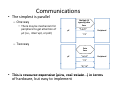
• The simplest is parallel
The simplest is parallel
Multiple (8 typically) data lines
– One way
• There may be mechanism for
peripheral to get attention of μC (i.e., interrupt, or poll)
μC
“L t h”
“Latch”
Peripheral
“CS”
– Two way
Data lines
μC
“Latch”
Peripheral
“CS”
“R/~W”
• This
This is resource expensive (pins, real
is resource expensive (pins real‐estate
estate…) in terms ) in terms
of hardware, but easy to implement
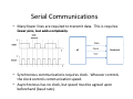
Serial Communications
Serial Communications
• Many fewer lines are required to transmit data. This is requires fewer pins but adds complexity
fewer pins, but adds complexity.
Data
μC
Clock
Peripheral
“CS”
• Synchronous communications requires clock. Whoever controls the clock controls communication speed.
• Asynchronous has no clock, but speed must be agreed upon beforehand (baud rate).
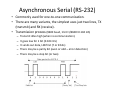
Asynchronous Serial (RS‐232)
• Commonly
Commonly used for one‐to‐one communication. used for one to one communication
• There are many variants, the simplest uses just two lines, TX (transmit) and RX (receive).
• Transmission process (9600 baud, 1 bit=1/9600=0.104 mS)
–
–
–
–
–
Transmit idles high (when no communication).
It
It goes low for 1 bit (0.104 mS)
l f 1 bit (0 104 S)
It sends out data, LSB first (7 or 8 bits)
There may be a parity bit (even or odd – error detection)
There may be a stop bit (or two)
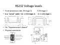
RS232 Voltage levels
• From processor side, 0V=logic 0, 3.3V=logic 1
In a “serial”
serial cable +12→+3V=logic 0, ‐3→‐12V=logic 1
cable +12→+3V=logic 0 ‐3→‐12V=logic 1
• In a • On “Experimenter’s board”
• Physical connector
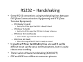
RS232 – Handshaking
RS232 • Some RS232 connections using handshaking lines between DCE (Data Communications Equipment) and DTE (Data (
q p
)
(
Terminal Equipment). – RTS (Ready To Send)
• Sent by the DTE to signal the DCE it is Ready To Send.
– CTS (Clear To Send)
• Sent by the DCE to signal the DTE that it is Ready to Receive.
– DTR (Data Terminal Ready)
• Sent to DTE to signal the DCE that it is ready to connect
– DSR (Data Set Read)
• Sent to DC to signal the DTE that it is ready to connect
• IIn practice if these handshaking lines are used it can be ti if th
h d h ki li
d it
b
difficult to set up the serial communications, but it is quite robust once working.
• There is also software handshaking (XON/XOFF)
• DTE and DCE have different connector pinouts.
MSP430 USCI in UART mode
(also USART peripheral)
UART mode features include:
• 7‐ or 8‐bit data; odd, even, or non‐parity
• Independent transmit and receive •LSB‐first or MSB‐first data •Receiver start‐edge detection for auto‐
d d
f
wake up from LPMx modes
•Independent interrupt capability for receive and transmit
receive and transmit
• Status flags for error detection and suppression
•Built‐in idle‐line and address‐bit communication protocols for p
y
multiprocessor systems
• Status flags for address detection
UART code
#include
"msp430xG46x.h"
//
//
//
//
//
//
//
//
//
//
//
Echo a received character, RX ISR used. Normal mode is LPM3,
USCI_A0 RX interrupt triggers TX Echo.
ACLK = BRCLK = LFXT1 = 32768, MCLK = SMCLK = DCO~1048k
Baud divider, 32768hz XTAL @9600= 32768/9600= 3.41(0003h 03h )
----------------/|\|
MSP430xG461x || |
XIN|- 32kHz
--|RST
XOUT||
P4.7/UCA0RXD|------------>
|
| 9600 - 8N1
|
P4
P4.6/UCA0TXD|<-----------6/UCA0TXD|<
void main(void)
{
volatile unsigned int i;
P4SEL |= 0x0C0;
UCA0CTL1 |= UCSSEL_1;
UCA0BR0 = 0x03;
UCA0BR1 = 0x00;
UCA0MCTL = 0x06;
UCA0CTL1 &= ~UCSWRST;
IE2 |= UCA0RXIE;
//
//
//
//
//
//
//
P4.7,6 = USCI_A0 RXD/TXD
CLK = ACLK
32k/9600 - 3.41
User’s manual has formulas for these
Modulation
**Initialize USCI state machine**
Enable USCI_A0 RX interrupt
_BIS_SR(LPM0_bits + GIE);
// Enter LPM0, interrupts enabled
}
// Echo back RXed character, confirm TX buffer is ready first
#pragma vector=USCIAB0RX_VECTOR
__interrupt
p void USCIA0RX_ISR (
(void)
)
{
while(!(IFG2&UCA0TXIFG));
// Make sure last character went out.
UCA0TXBUF = UCA0RXBUF;
// TX -> RXed character
}
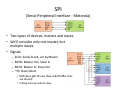
SPI
(Serial Peripheral Interface ‐ Motorola)
(Serial Peripheral Interface • Two types of devices, masters and slaves. • We’ll consider only one master, but ’
multiple slaves.
• Signals
–
–
–
–
SCLK: Serial CLocK, set by Master
MOSI: Master Out, Slave In
MISO: Master In, Slave Out
~SS: Slave Select
• EEach slave gets its own slave select (other lines h l
t it
l
l t ( th li
are shared)
• Pulling line low selects slave
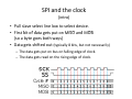
SPI and the clock
(intro)
• Pull slave select line low to select device.
• First bit of data gets put on MISO and MOSI i bi f d
SO d OS
(so a byte goes both ways)
• Data gets shifted out D t
t hift d t (typically 8 bits, but not necessarily)
( i ll 8 bi b
il )
– The data gets put on bus on falling edge of clock.
– The data gets read on the rising edge of clock.
The data gets read on the rising edge of clock
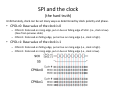
SPI and the clock
(the hard truth)
(the hard truth)
Unfortunately, clock can be set many ways as determined by clock polarity and phase.
• CPOL=0: Base value of the clock is 0
– CPHA=0: Data read on rising edge, put on bus on falling edge of SCLK. (i.e., clock is low).
(Case from previous slide)
– CPHA=1: Data read on falling edge, put on bus on rising edge (i.e., clock is high).
• CPOL=1: Base value of the clock is 1
– CPHA=0: Data read on falling edge, put on bus on rising edge (i.e., clock is high).
– CPHA=1: Data read on rising edge, put on bus on falling edge (i.e., clock is low).
g g ,p
g g ( ,
)
SPI and SCI
SPI mode features include:
• 7‐ or 8‐bit data length
• LSB‐first or MSB‐first data
LSB‐first or MSB‐first data
• Master or slave modes
• Selectable clock polarity and phase control
d h
t l
• Programmable clock frequency in master mode
• Independent transmit and receive
• Continuous transmit and receive
• Independent interrupt capability for receive and p
y
transmit
• Slave operation in LPM4
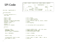
SPI Code
#include
"msp430xG46x.h"
// MCLK = SMCLK = default DCO ~1048k, BRCLK = SMCLK/2
//
---------------------//
/|\|
MSP430xG461x
|
//
TLC549
| |
XIN |32kHz
//
--------------|RST
XOUT|//
|
CS|<---|P3.0
|
//
|
DATAOUT|--->|P3.2/UCB0SOMI
|
// ~>| IN+ I/O CLK|<---|P3.3/UCB0CLK
P5.1|--> LED
void main(void)
{
volatile unsigned int i;
char data;
P5DIR |= 0x02;
P3SEL |= 0x0C;
P3DIR |= 0x01;
UCB0CTL0 |= UCMST+UCSYNC+UCMSB;
UCB0CTL1 |= UCSSEL_2;
UCB0BR0 = 0x02;
UCB0BR1 = 0;
UCB0CTL1
0
1 &= ~UCSWRST;
while(1)
{
P3OUT &= ~0x01;
UCB0TXBUF = 0x00;
while (!(IFG2 & UCB0RXIFG));
}
}
//
//
//
//
//
//
P5.1 output
P3.3,2 option
p
select
P3.0 output direction
8-bit SPI mstr, MSb 1st, CPOL=0, CPHS=0
SMCLK
Set Frequency
// **
**Initialize
i i li
USCI state machine**
hi **
// Enable TLC549 (A/D) , ~CS (~SS) reset
// Dummy write to start SPI
// USCI_B0 RX buffer ready?
data = UCB0RXBUF;
// data = 00|DATA
P3OUT |= 0x01;
// Disable TLC549, ~CS (~SS) set
if(data>=0x7F) P5OUT |= 0x02;
else P5OUT &= ~0x02;
// data = AIN > 0.5(REF+ - REF-)?
// LED off
LED On
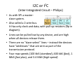
I2C or I2C
((Inter‐Integrated Circuit –
g
Philips)
p)
• As with SPI a master‐
slave system.
y
• Also called a 2‐wire bus.
It Has only clock and data, with pull‐up resistors (Rp
y
,
p
p
( p in diagram).
• Lines can be pulled low by any device, and are high when all devices release them.
• There are no “slave‐select” lines – instead the devices have “addresses” that are sent as part of the transmission protocol.
• Four max speeds (100 kbS (standard), 400 kbS (fast), 1 MbS (fast plus), and 3.4 MbS (high‐speed)
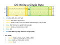
I2C Write a Single Byte
1.
2
2.
3.
4.
5.
6.
7.
•
All: allow SDA, SCL start high
M
Master: SDA low to signal start
SDA l
i l
Master: Send out SCL, and 7 bit address followed by 0 (~W) on SDA
Slave: Pull SDA low to signify ACKnowledge
Master: Send out 8 data bits on SDA
Slave: Ack
All: allow SDA to go high when SCL is high (stop)
allow SDA to go high when SCL is high (stop)
For “Read”, 3
3.
M t Address following by 1 (R) on SDA
Master:
Add
f ll i b 1 (R)
SDA
5. Slave: Send out 8 data bits on SDA
6. Master: Ack
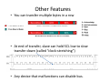
Other Features
• You can transfer multiple bytes in a row
You can transfer multiple bytes in a row
•
• At
At end of transfer, slave can hold SCL low to slow end of transfer slave can hold SCL low to slow
transfer down (called “clock‐stretching”)
• Any device that malfunctions can disable bus.
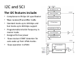
I2C and SCI
The I2C features include:
• Compliance to Philips I2C specification
• Slave receiver/transmitter mode
Sl
i /t
itt
d
• Standard mode up to 100 kbps and fast mode up to 400 kbps support
• Programmable UCxCLK frequency in master mode
• Designed for low power
Designed for low power
• Slave receiver START detection for auto‐wake up from LPMx modes
• Slave operation in LPM4
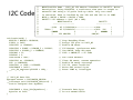
I2C Code
//
//
//
//
//
//
//
//
//
//
//
//
MSP430xG461x Demo - USCI_B0 I2C Master Interface to DAC8571, Write
Description: Using UCB0TXIE, a continuous sine wave is output to
external DAC using a 16-point look-up table. Only one start
is executed. Data is handled by the ISR and the CPU is in LPM0.
MCLK = SMCLK = TACLK = BRCLK = 1MHz
DAC8571 I2C address = 0x4C (A0 = GND)
MSP430xG461x
DAC8571
-----------------------------|XIN
P3.1/UCB0SDA|<--------------->|SDA
|
32kHz |
P3.2/UCB0SCL|---------------->|SCL I2C
|
-|XOUT
|XOUT
|
|
SLAVE
|
|
I2C MASTER
|
GND|A0
|
void main(void) {
WDTCTL = WDTPW + WDTHOLD;
P3SEL |= 0x06;
UCB0CTL1 |= UCSWRST;
UCB0CTL0 = UCMST + UCMODE_3 + UCSYNC;
UCB0CTL1 = UCSSEL_2 + UCSWRST;
UCB0BR0 = 11;
UCB0BR1 = 0;
UCB0I2CSA = 0x4c;
UCB0CTL1 &= ~UCSWRST;
IE2 |= UCB0TXIE;
UCB0CTL1 |= UCTR + UCTXSTT;
UCB0TXBUF = 0x010;
__bis_SR_register(CPUOFF
g
(
+ GIE);
);
}
//
//
//
//
//
//
Stop Watchdog Timer
Assign I2C pins to USCI_B0
Enable SW reset
I2C Master, synchronous mode
Use SMCLK, keep SW reset
fSCL = SMCLK/11 = 95.3kHz
//
//
//
//
//
//
Set slave address
Clear SW reset, resume operation
Enable TX ready interrupt
I2C TX, start condition
Write DAC control byte
Enter LPM0 w/
/ interrupts
p
// USCI_B0 Data ISR
#pragma vector = USCIAB0TX_VECTOR
__interrupt void USCIAB0TX_ISR(void) {
static unsigned char ByteCtr;
UCB0TXBUF = Sine_Tab[ByteCtr++];
ByteCtr &= 0x1f;
}
// Transmit data byte
// Do not exceed table
Wireless
• Order: Increasing complexity, power and bandwidth
g
p
y, p
–
–
–
–
SimpliciTI: <200 kbS
Zigbee (IEEE 802.15.4): 250 kbS
Bluetooth (IEEE 802 15 1): 1 MbS – 24 MbS
Bluetooth (IEEE 802.15.1): 1 MbS
24 MbS
WiFi (IEEE 802.11): b 11 MbS; g 54 MbS; n 150 MbS
• Data rates needed
– Voice: 4 kbS
Voice: 4 kbS
– Music: 700 kbS
– Video: 3.5 MbS Standard; 40 MbS Blu‐ray
References
•
•
•
•
•
•
•
•
•
MSP430x4xx Family User’s Guide http://focus.ti.com/lit/ug/slau056j/slau056j.pdf
MSP430FG4618/F2013 E
MSP430FG4618/F2013 Experimenter’s Board User’s Guide http://focus.ti.com/lit/ug/slau213a/slau213a.pdf
i
’ B d U ’ G id h //f
i
/li / / l 213 / l 213 df
Serial Comm image http://www.ee.nmt.edu/~rison/ee308_spr99/supp/990406/sync_serial.gif
RS‐232 byte image http://www.eeherald.com/images/rs232‐3.jpg
RS‐232 Connector Image http://www.bisque.com/tom/bluetooth/Images/db9.jpg
SPI http://en.wikipedia.org/wiki/Serial_Peripheral_Interface_Bus
I2C: http://en.wikipedia.org/wiki/I%C2%B2C
I2C: http://www.best‐microcontroller‐projects.com/i2c‐tutorial.html
I2C: http://www.eetimes.com/design/analog‐design/4010395/SIGNAL‐CHAIN‐BASICS‐Part‐32‐‐Digital‐
interfaces‐con‐t‐‐‐The‐I2C‐Bus