1
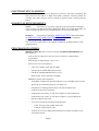
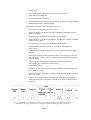
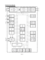
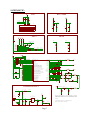
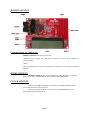
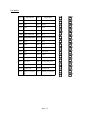
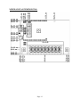
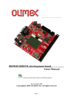
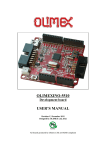
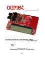
MSP430-CCRFLCD development board Users Manual All boards produced by Olimex are ROHS compliant Revision A, November 2011 Copyright(c) 2011, OLIMEX Ltd, All rights reserved Page 1 INTRODUCTION: MSP430-CCRFLCD is development board with CC430F5137IRGZ microcontroller from Texas Instruments. This ultra-low-power microcontroller has integrated CC1101 RF transceiver. The board has also LCD, two status leds, two user buttons and UEXT, which can be modified as device or host. MSP430-CCRFLCD can communicate with other boards with integrated CC1101 RF transceiver via radio connection. BOARD FEATURES: • Microcontroller: CC430F5137IRGZ • JTAG • UEXT • LCD 1x9 • LIPO_BAT connector for Lithium-ion polymer battery which permits outdoor communication between two or more MSP430-CCRFLCD boards • on-board voltage regulator • On-bard pcb antenna • Supported radio frequencies bands 868/915 MHz – software selectable. By default – 868 MHz. • Maximal permissible distance between two MSP430-CCRFLCD boards depends on RF chip's output power, data transfer rate and the selected radio frequency band. For more information, see the table below. Results given there are taken via using 2 MSP430-CCRF boards, but because of the slight difference between MSP430-CCRF and MSP430CCRFLCD we are expecting results closer to this! • two user buttons • two status leds • RTC crystal • extension pin holes for most of the microcontroller pins • FR-4, 1.00 mm, soldermask, component print • Dimensions: 84.84 x 63.50mm (3.34 x 2.50") RF Frequency Output Power Data Rate Measured Distance 868MHz 10dBm 1.2kBaud 155m 868MHz 10dBm 38.4kBaud 110m 868MHz 10dBm 250kBaud 85m 915MHz 10dBm 1.2kBaud 140m 915MHz 10dBm 38.4kBaud 100m 915MHz 10dBm 250kBaud 60m This measurements were taken via using “RF Connection_toggle LED” demo software loaded at two alike MSP430-CCRF boards! Page 2 ELECTROSTATIC WARNING: The MSP430-CCRFLCD board is shipped in protective anti-static packaging. The board must not be subject to high electrostatic potentials. General practice for working with static sensitive devices should be applied when working with this board. BOARD USE REQUIREMENTS: Cables: The cable you will need depends on the programmer/debugger you use. If you use MSP-JTAG-TINY, MSP-JTAG-TINY-V2, or MSP-JTAG-ISO, you will need USB A-B cable. If you use MSP-JTAG, you will need LPT cable. Hardware: Programmer/Debugger MSP-JTAG-TINY, MSP-JTAG-TINYV2, MSP-JTAG-ISO, MSP-JTAG, MSP-JTAG-RF, or other compatible programming/debugging tool. You can also use other Olimex's board MSP-CCRFLCD, or MSP-CCRF for radio communication. PROCESSOR FEATURES: MSP430-CCRFLCD board use microcontroller CC430F5137IRGZFBD100 with these features: − True System-on-Chip (SoC) for Low-Power Wireless Communication Applications − Wide Supply Voltage Range: 1.8 V to 3.6 V − Ultra-Low Power Consumption: − − CPU Active Mode (AM): 160 μA/MHz − Standby Mode (LPM3 RTC Mode):2.0 μA − Off Mode (LPM4 RAM Retention): 1.0 μA − Radio in RX: 15 mA, 250 kbps, 915 MHz MSP430™ System and Peripherals − 16-Bit RISC Architecture, Extended Memory, up to 20-MHz System Clock − Wake-Up From Standby Mode in Less Than 6 μs − Flexible Power Management System with SVS and Brownout − Unified Clock System with FLL − 16-Bit Timer TA0, Timer_A with Five Capture/Compare Registers − 16-Bit Timer TA1, Timer_A with Three Capture/Compare Registers − Hardware Real-Time Clock − Two Universal Serial Communication Interfaces − − USCI_A0 supporting UART, IrDA, SPI − USCI_B0 supporting I2C, SPI 12-Bit A/D Converter With Internal Reference, Sample-and-Hold, and Autoscan Features Page 3 − − Comparator − 128-bit AES Security Encryption/Decryption Coprocessor − 32-Bit Hardware Multiplier − Three-Channel Internal DMA − Serial Onboard Programming, No External Programming Voltage Needed − Embedded Emulation Module (EEM) High-Performance Sub-1-GHz RF Transceiver Core − Wide Supply Voltage Range: 2.0 V to 3.6 V − Frequency Bands: 300 MHz to 348 MHz, 389 MHz to 464 MHz, and 779 MHz to 928 MHz. − Programmable Data Rate From 0.6 kBaud to 500 kBaud − High Sensitivity (-117 dBm at 0.6 kBaud, -111 dBm at 1.2 kBaud, 315 MHz, 1% Packet Error Rate) − Excellent Receiver Selectivity and Blocking Performance − Programmable Output Power Up to +12 dBm for All Supported Frequencies − 2-FSK, 2-GFSK, and MSK Supported as well as OOK and Flexible ASK Shaping − Flexible Support for Packet-Oriented Systems: On-Chip Support for Sync Word Detection, Address Check, Flexible Packet Length, and Automatic CRC Handling − Support for Automatic Clear Channel Assessment (CCA) Before Transmitting (for Listen-Before-Talk Systems) − Digital RSSI Output − Suited for Systems Targeting Compliance With EN 300 220 (Europe) and FCC CFR Part 15 (US) − Suited for Systems Targeting Compliance With Wireless M-Bus Standard EN 13757-4:2005 − Support for Asynchronous and Synchronous Serial Receive/Transmit Mode for Backward Compatibility With Existing Radio Communication Protocols (1) 5, 3 - represents two instantiations of Timer_A, the first instantiation having 5 and the second instantiation having 3 capture compare registers and PWM output generators, respectively. Page 4 BLOCK DIAGRAM: Page 5 MEMORY ORGANIZATION: (1) All memory regions not specified here are vacant memory, and any access to them causes a Vacant Memory Interrupt. Page 6 SCHEMATIC: LCD 3.3V BUTTONS 3.3V R21 4.7k R20 4.7k 3.3V C35 100nF LCD_SCL LCD_SDA R17 33k R18 33k 1 2 3 LCD BUT2 R16 1k VSS VDD SCL SDA 4 BUT1 R7 1k C34 BUT1 C36 BUT2 100nF T1157 100nF T1157 LCD-CL010-4042-01 3.3V 3.3V 3.3V UEXT 3.3V LEDS R4 J1 1-2:Open; 2-3:Close J2 LED1 1-2:Open; 2-3:Close 1 2 3 LED2 3 2 1 UEXT-1 UEXT-2 UEXT-3 UEXT-4 UEXT-5 UEXT-6 UEXT-7 UEXT-8 UEXT-9 UEXT-10 LED1 BSLTX/UCA0TXD BSLRX/UCA0RXD SCL SDA UCB0_MISO/SCL UCB0_MOSI/SDA UCB0_CLK UCB0_STE R9 R8 NA NA R10 R11 0R 0R 0R(NA) 0R(NA) R15 1k SW_SCL SW_SDA LED2 R19 1k GREEN(GYX-SD-TC0805SGC) R6 4.7k RED(GYX-SD-TC0805SURK) R5 4.7k 33k BH10R 1k C1 2.2nF R3 33k C 12 C13 C14 10uF/6.3V + C1 1 100nF 34 27 28 31 32 26 RF_XOUT 25 RF_XIN R_BIAS VCORE 10uF/6.3V C1 0 + 3.3V C9 33 7 CC430F5137IRGZ L2 3.3V C21 100nF C20 FB0805/600R/200mA(201209-601) 30 RF_N 29 RF_P P3.0/PM_CBOUT0/PM_TA0CLK P3.1/PM_TA0CCR0A P3.2/PM_TA0CCR1A P3.3/PM_TA0CCR2A P3.4/PM_TA0CCR3A P3.5/PM_TA0CCR4A P3.6/PM_RFGDO1 P3.7/PM_SMCLK 3.3V VSS 100nF P2.0/PM_CBOUT1/PM_TA1CLK/CB0/A0 P2.1/PM_TA1CCR0A/CB1/A1 P2.2/PM_TA1CCR1A/CB2/A2 P2.3/PM_TA1CCR2A/CB3/A3 P2.4/PM_RTCCLK/CB4/A4/VREF-/VEREFP2.5/PM_SVMOUT/CB5/A5/VREF+/VEREF+ P2.6/PM_ACLK/(RF_ATEST) P2.7/PM_MODCLK/PM_DMAE0 GN D QCT32768/6pF 100nF VSS GUARD AVCC_RF AVCC_RF AVCC_RF AVCC_RF Q1 10uF/6.3V FB0805/600R/200mA(201209-601) C7 NA C8 NA + 8 DVCC 22 DVCC 41 DVCC + 43 100nF C19 LCD_SCL LCD_SDA 21 20 19 18 17 16 15 14 P5.1/XOUT P1.0/PM_RFGDO0 P1.1/PM_RFGDO2 P1.2/PM_UCB0SOMI/PM_UCB0SCL P1.3/PM_UCB0SIMO/PM_UCB0SDA P1.4/PM_UCB0CLK/PM_UCA0STE P1.5/PM_UCA0RXD/PM_UCA0SOMI P1.6/PM_UCA0TXD/PM_UCA0SIMO P1.7/PM_UCA0CLK/PM_UCB0STE/(ROSC) C6 100nF 2 1 2 1 P3.0 P3.1 P3.2 P3.3 P3.4 P3.5 P3.6 P3.7 LED2 BUT2 3 2 1 48 47 46 24 23 42 AVSS 44 P5.0/XIN C5 C18 SW_SCL SW_SDA SENS_E BAT P2.0 P2.1 P2.2 P2.3 P2.4 P2.5 P2.6 P2.7 PIN HN1x2(Close) 13 12 11 10 9 6 5 4 L1 45 2pF POUT HN1x2(Open) LED1 BUT1 UCB0_MISO/SCL UCB0_MOSI/SDA UCB0_CLK BSLRX/UCA0RXD BSLTX/UCA0TXD UCB0_STE AVCC C17 P1.0 P1.1 P1.2 P1.3 P1.4 P1.5 P1.6 P1.7 #RST/NMI/SBWTDIO TEST/SBWTCK PJ.3/TCK PJ.2/TMS PJ.1/TDI/TCLK PJ.0/TDO 100nF PJ.3 PJ.2 PJ.1 PJ.0 40 39 38 37 36 35 100nF BH14S U1 #RST/SBWTDIO TEST/SBWTCK TCK TMS TDI TDO 10uF/6.3V 13 11 9 7 5 3 1 C16 JTAG 14 12 10 8 6 4 2 RST TEST R2 C15 33k 2pF R1 100nF 3.3V C26 1.5pF/+-0.25pF/COG L3 L6 12nH/5%(ELJRE12NJFA/1198377) C22 10pF Q3 R12 GND GND 56k/1% L7 18nH/5%(ELJRE18NJFA/1198379) 12nH/5%(ELJRE12NJFA/1198377) C25 1pF/+-0.25pF/COG L4 C23 10pF C24 470nF C29 C27 12nH/5%(ELJRE12NJFA/1198377) 3.3pF/+-0.25pF/COG 1.5pF/+-0.25pF/COG L5 C28 100pF/5%/COG 18nH/5%(ELJRE18NJFA/1198379) TSX-3225/26MHz/10PPM/9pF/3.2x2.5mm SMD ANT POWER SUPPLY R25 (2.5V) BAT Monopole_PCB_Antenna R13 SENS_E 56k/1% C37 100nF R24 47k/1% GND. GND (4.6V) C2 100nF 2 C3 10uF/6.3V VOUT 1 3.3V VIN GND 3 + DW02R VR MCP1700T-3302E/MB VIN + 1 2 0R(NA) C30 L8 12nH/5%(ELJRE12NJFA/1198377) C32 C31 NA NA 100pF/5%/COG 3.3V 3.7V LIPO_BAT + - 0R C33 C4 10uF/6.3V 100nF MSP430-CCRFLCD Rev.B COPYRIGHT(C) 2011, OLIMEX LTd. R14 0R 0R(NA) Page 7 http://www.olimex.com/dev BOARD LAYOUT: POWER SUPPLY CIRCUIT: MSP430-CCRFLCD can take power from: –External power supply via LIPO_BAT connector 3.7 VDC from Lithium-ion polymer battery –JTAG The programmed board power consumption is about 20 mA with all peripherals enabled. RESET CIRCUIT: MSP430-CCRFLCD reset circuit includes R1 (33k), R2 (1kΩ), C1 (2..2nF), JTAG pin 11 and CC430F5137IRGZ pin 40 (#RST/NMI/SBWTDIO). CLOCK CIRCUIT: Quartz crystal Q1 32.768 kHz is connected to CC430F5137IRGZ pin 44 (P5.0/XIN) and pin 43 (P5.1/XOUT). Quartz crystal Q3 26 MHz is connected to CC430F5137IRGZ pin 25 (RF_XIN) and pin 26 (RF_XOUT). Page 8 JUMPER DESCRIPTION: Power In jumper: P_IN jumper connects power supply from JTAG connector. You have to ensure that your circuit doesn't draw more than few milliamperes current or the power supply may decrease due to the JTAG port current limitations. P_IN is useful and must be used mostly to program the microcontroller. Power Out jumper: P_OUT jumper connects power from MSP430-CCRFLCD to JTAG connector. When this jumper cap is placed, the power supply of JTAG connector will follow the power supply of the board. This is useful when your board works at lower than +3,3V power supply. Note: P_IN and P_OUT jumper caps should not be placed at the same time. J1 This jumper, when is in position 1-2 – UEXT pin 3 (signal TX) is connected to CC430F5137IRGZ pin 5 (signal BSLTX/UCA0TXD); when the jumper is in position 2-3 - UEXT pin 3 (signal TX) is connected to CC430F5137IRGZ pin 6 (signal BSLRX/UCA0RXD) Default state is shorted in position 2-3. J2 This jumper, when is in position 1-2 – UEXT pin 4 (signal RX) is connected to CC430F5137IRGZ pin 6 (signal BSLRX/UCA0RXD); when the jumper is in position 2-3 - UEXT pin 4 (signal RX) is connected to CC430F5137IRGZ pin 5 (signal BSLTX/UCA0TXD) Default state is shorted in position 2-3. When jumpers J1 and J2 are shorted in position 1-2 – the board is configured as host and can be used as host for some of our module boards. When these jumpers are shorted in position 2-3 – the board is configured as device and can be used as module board. INPUT/OUTPUT: Status Led with name LED1 (red) connected to CC430F5137IRGZ pin 13 (P1.0/PM_RFGDO0). Status Led with name LED2 (green) connected to CC430F5137IRGZ pin 24 (P2.6/PM_ACLK). User button with name BUT1 connected to CC430F5137IRGZ pin 12 (P1.1/PM_RFGDO2). User button with name BUT2 connected to CC430F5137IRGZ pin 23 (P2.7/PM_MODCLK). LCD 1x9 – 9 segments LCD without font generator Page 9 EXTERNAL CONNECTORS DESCRIPTION: JTAG: Pin # Signal Name Pin # Signal Name 1 TDO 2 JTAG power supply 3 TDI 4 VCC 5 TMS 6 Not Connected 7 TCK 8 TEST/SBWTCK 9 GND 10 Not Connected 11 #RST/SBWTDIO 12 BSLTX/UCA0TXD 13 Not Connected 14 BSLRX/UCA0RXD LIPO_BAT: Pin # Signal Name 1 VIN 2 GND Page 10 UEXT: Pin # Signal Name 1 VCC 2 GND 3 TX 4 RX 5 SCL 6 SDA 7 UCB0_MISO/SC L 8 UCB0_MOSI/SD A 9 UCB0_CLK 10 UCB0_STE Page 11 Pin holes: Pin # Signal Name Pin # Signal Name PJ.0 TDO P2.6 LED2 PJ.1 TDI P2.7 BUT2 PJ.2 TMS P3.0 P3.0 PJ.3 TCK P3.1 P3.1 TEST TEST/SBWTCK P3.2 P3.2 RST #RST/SBWTDIO P3.3 P3.3 3.3V VCC P3.4 P3.4 GND GND P3.5 P3.5 P2.5 P2.5 P3.6 LCD_SCL P2.4 P2.4 P3.7 LCD_SDA P2.3 BAT P1.0 LED1 P2.2 SENS_E P1.1 BUT1 P2.1 SW_SDA P1.2 UCB0_MISO/SCL P2.0 SW_SCL P1.3 UCB0_MOSI/SDA P1.7 UCB0_STE P1.4 UCB0_CLK P1.6 BSLTX/UCA0TX D P1.5 BSLRX/UCA0RXD Page 12 MECHANICAL DIMENSIONS: Page 13 AVAILABLE DEMO SOFTWARE: Blinking Leds sourced by DCO - leads "MSP430-CCRFLCD's" on-board "LED1" and "LED2" to blink with frequency ~ 1Hz. When "LED1" is on "LED2" is off and vice-versa. Clock source -> DCO. Blinking Leds sourced by RTC - leads "MSP430-CCRFLCD's" on-board "LED1" and "LED2" to blink with frequency ~ 1Hz. When "LED1" is on "LED2" is off and vice-versa. Clock source -> crystal 32.768kHz. Blinking Leds sourced by RTC and USART Echo - MSP430-CCRFLCD's onboard "LED1" and "LED2" are blinking again with frequency ~ 1Hz. by RTC and USART Echo" If USART has received a character, then it returns echo. Toggle LEDx when BUTx is pressed - When BUT1 is pressed then LED1 is switched over. When BUT2 is pressed then LED2 is switched over. Buttons and LCD - Visualize at LCD which one button you have pressed RF Connection_ press BUT - This example realize simple RF connection between 2 MSP430-CCRFLCD boards. Pressing BUT1 at the first board will toggle LED1 at the second board and vice-versa! RF Connection_toggle LED - This example again realize simple RF connection between 2 MSP430-CCRFLCD boards. Both boards are sending ~4 packets per second with length 10 bytes. Whenever any board has received a valid packet, it switches-over its LED1! Packet sending can be enabled/disabled individually for everyone board by pressing its button BUT1. Page 14 ORDER CODE: MSP430-CCRFLCD - assembled and tested board How to order? You can order to us directly or by any of our distributors. Check our web www.olimex.com/dev for more info. Revision history: Board's revision: Rev. B, May 2011 Manual's revision: Rev. Initial, September 2011 Rev. A, November 2011 - BOARD FEATURES – added is table which describes maximal permissible distance between two MSP430-CCRF boards versus different RF settings. MSP430-CCRFLCD is slightly different from MSP430CCRF so we are expecting closer results. - SCHEMATIC – is updated to last version – with changed C22 and C23 values from 15pF to 10pF. - AVAILABLE DEMO SOFTWARE - “RF Connection” is changed to “RF Connection_ press BUT”. “RF Connection_toggle LED” was added. Page 15 Disclaimer: © 2011 Olimex Ltd. All rights reserved. Olimex®, logo and combinations thereof, are registered trademarks of Olimex Ltd. Other terms and product names may be trademarks of others. The information in this document is provided in connection with Olimex products. No license, express or implied or otherwise, to any intellectual property right is granted by this document or in connection with the sale of Olimex products. Neither the whole nor any part of the information contained in or the product described in this document may be adapted or reproduced in any material from except with the prior written permission of the copyright holder. The product described in this document is subject to continuous development and improvements. All particulars of the product and its use contained in this document are given by OLIMEX in good faith. However all warranties implied or expressed including but not limited to implied warranties of merchantability or fitness for purpose are excluded. This document is intended only to assist the reader in the use of the product. OLIMEX Ltd. shall not be liable for any loss or damage arising from the use of any information in this document or any error or omission in such information or any incorrect use of the product. Page 16