1
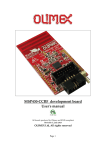
MSP430-H2274 development board
Users Manual
All boards produced by Olimex are ROHS compliant
Rev.A, Jully 2009
Copyright(c) 2009, OLIMEX Ltd, All rights reserved
Page 1
INTRODUCTION
MSP430-H2274 header board provides easy way for developing and prototyping
with the new MSP430F2274 ultralow-power, mixed signal microcontroller produced
by Texas Instruments.
MSP430-H2274 has JTAG port for programming and debugging and most of the
GPIOs are on extension headers where you can connect your additional circuits.
BOARD FEATURES
-
CPU: MSP430F2274 mixed signal microcontroller
JTAG connector
JTAG Power_In and Power_Out jumpers
32768 Hz crystal oscillator
Two extension connectors – HN19x1
PCB: FR-4, 1.5 mm (0,062"), solder mask, silkscreen component print
Dimensions: 56.2x 19.5mm ( 2.21x 0.77")
ELECTROSTATIC WARNING
The MSP430-H2274 board is shipped in protective anti-static packaging. The board
must not be subject to high electrostatic potentials. General practice for working
with static sensitive devices should be applied when working with this board.
BOARD USE REQUIREMENTS
Cables: The cable you will need depends on the programmer/debugger you use. If
you use MSP430-JTAG, you will need LPT cable, if you use MSP430-JTAG-TINY or
MSP-JTAG-ISO, you will need A-B USB cable, if you use MSP430-JTAG-RF, you can
connect it to the USB port of your computer, or via USB cable type A – female.
Hardware: Programmer/Debugger – one of our Programmers – MSP430-JTAG,
MSP430-JTAG-TINY, MSP430-JTAG-ISO, or MSP430-JTAG-RF.
Software: MSP430 KickStart software.
Page 2
PROCESSOR FEATURES
MSP430-H2274 board use ultralow-power mixed signal microcontroller with two
built-in 16-bit timers, a universal serial communication interface, 10-bit A/D
converter with integrated reference and data transfer controller (DTC), two generalpurpose operational amplifiers, 32 GPIO with these features:
–
32KB + 256B Flash Memory
–
1KB RAM
–
Low Supply Voltage Range: 1.8 V to 3.6 V
–
Ultralow Power Consumption
–
Active Mode: 270 µA at 1 MHz, 2.2 V
–
Standby Mode: 0.7 µA
–
Off Mode (RAM Retention): 0.1 µA
–
Ultrafast Wake-Up From Standby Mode in Less Than 1 µs
–
16-Bit RISC Architecture, 62.5-ns Instruction Cycle Time
–
Basic Clock Module Configurations:
–
Internal Frequencies up to 16 MHz With Four Calibrated Frequencies to
±1%
–
Internal Very-Low-Power Low-Frequency Oscillator
–
32-kHz Crystal
–
High-Frequency Crystal 16 MHz
–
Resonator
–
External Digital Clock Source
–
External Resistor
–
16-Bit Timer_A With Three Capture/Compare Registers
–
16-Bit Timer_B With Three Capture/Compare Registers
–
Universal Serial Communication Interface
–
Enhanced UART Supporting Auto-Baudrate Detection (LIN)
–
IrDA Encoder and Decoder
–
Synchronous SPI
–
I2CTM
–
10-Bit 200-ksps Analog-to-Digital (A/D) Converter With Internal
Reference,Sample-and-Hold, Autoscan, and Data Transfer Controller
–
Two Configurable Operational Amplifiers
–
Brownout Detector
–
Serial Onboard Programming, No External Programming Voltage Needed
Programmable Code Protection by Security Fuse
–
Bootstrap Loader
–
On Chip Emulation Module
Page 3
BLOCK DIAGRAM
Page 4
MEMORY ORGANIZATION
Page 5
Page 6
10p(NA)
G ND
C5
100n
10p(NA)
Q1
32768/6pF
C4
1
2
3
4
5
6
7
8
9
10
11
12
13
14
15
16
17
18
19
HN19x1
1
2
3
4
5
6
7
8
9
10
11
12
13
14
15
16
17
18
19
CON1
C2
1n
R2
HN1x2
33K
2
1
C3
http://www.olimex.com/dev
COPYRIGHT(C), 2009
Rev. A
MSP430-H2274
P_OUT
0R
R3
0R(NA)
0R
R4
0R(NA)
C1
100n
P_IN
HN2x7
JTAG
MSP430F2274H
TEST/SBWTCK
DVCC
P2.5/ROSC
DVSS
XOUT/P2.7
XIN/P2.6
#RST/NMI/SBWTDIO
P2.0/ACLK/A0/OA0I0
P2.1/TAINCLK/SMCLK/A1/OA0O
P2.2/TA0/A2/OA0I1
P3.0/UCB0STE/UCA0CLK/A5
P3.1/UCB0SIMO/UCB0SDA
P3.2/UCB0SOMI/UCB0SCL
P3.3/UCB0CLK/UCA0STE
AVSS
AVCC
P4.0/TB0
P4.1/TB1
P4.2/TB2
U1
1
2
3
4
5
6
7
8
9
10
11
12
13
14
15
16
17
18
19
2
4
6
8
10
12
14
P1.7/TA2/TDO/TDI
P1.6/TA1/TDI
P1.5/TA0/TMS
P1.4/SMCLK/TCK
P1.3/TA2
P1.2/TA1
P1.1/TA0
P1.0/TACLK/ADC10CLK
P2.4/TA2/A4/VREF+/VEREF+/OA1I0
P2.3/TA1/A3/VREF-/VEREF-/OA1I1/OA1O
P3.7/A7/OA1I2
P3.6/A6/OA0I2
P3.5/UCA0RXD/UCA0SOMI
P3.4/UCA0TXD/UCA0SIMO
P4.7/TBCLK
P4.6/TBOUTH/A15/OA1I3
P4.5/TB2/A14/OA0I3
P4.4/TB1/A13/OA1O
P4.3/TB0/A12/OA0O
1
3
5
7
9
11
13
38
37
36
35
34
33
32
31
30
29
28
27
26
25
24
23
22
21
20
CON2
HN19x1
19
18
17
16
15
14
13
12
11
10
9
8
7
6
5
4
3
2
1
38
37
36
35
34
33
32
31
30
29
28
27
26
25
24
23
22
21
20
SCHEMATIC
2
1
HN1x2
33K
R1
BOARD LAYOUT
POWER SUPPLY CIRCUIT
MSP430-H2274 power supply depends on the state of jumpers P_IN and P_OUT.
VCC_IN goes on JTAG connector pin 2 and VCC_OUT goes on JTAG connector pin
4.
RESET CIRCUIT
MSP430-H2274 reset circuit includes pin 11of JTAG connector, pin 7 of Extension
connector - CON1, MSP430F2274 pin 7.
CLOCK CIRCUIT
Quartz crystal 32768MHz is connected to MSP430F2274 pin 5 (XOUT/P2.7) and
pin 6 (XIN/P2.6).
JUMPER DESCRIPTION
Power In jumper:
P_IN jumper connects power supply from JTAG connector to Header
board. When this jumper cap is placed you can program the microcontroller even
without any other external supply. Note that if the Header board is placed in target
circuit, you have to ensure that your circuit doesn't draw more than few
milliampers current or the power supply may decrease due to the JTAG port
current limitations. P_IN is useful and must be used mostly to program your
header board when it's not put on your target circuit socket.
Power Out jumper:
P_OUT jumper connects power from Header board to JTAG connector.
When this jumper cap is placed, the power supply of JTAG connector will follow
the power supply of Header board. This is useful when your Header board (target
circuit) works at lower than +3,3V power supply.
Note:
P_IN and P_OUT jumper caps should not be placed at the same time.
Page 7
CONNECTOR DESCRIPTIONS
JTAG
Pin #
Signal Name
Pin #
Signal Name
1
TDO
2
VCC_IN
3
TDI
4
VCC_OUT
5
TMS
6
NC
7
TCK
8
TEST/SBWTCK
9
GND
10
NC
11
#RST/NMI
12
NC
13
NC
14
NC
Pin #
Signal Name
Pin #
Signal Name
1
TEST/SBWTCK
2
DVCC
3
P2.5
4
DVSS
5
XOUT/P2.7
6
XIN/P2.6
7
#RST/NMI
8
P2.0
9
P2.1
10
P2.2
11
P3.0
12
P3.1
13
P3.2
14
P3.3
15
AVSS
16
AVCC
17
P4.0
18
P4.1
19
P4.2
CON1
Page 8
CON2
Pin #
Signal Name
Pin #
Signal Name
20
P4.3
21
P4.4
22
P4.5
23
P4.6
24
P4.7
25
P3.4
26
P3.5
27
P3.6
28
P3.7
29
P2.3
30
P2.4
31
P1.0
32
P1.1
33
P1.2
34
P1.3
35
P1.4/TCK
36
P1.5/TMS
37
P1.6/TDI
38
P1.7/TDO
Page 9
MECHANICAL DIMENSIONS
Page 10
AVAILABLE DEMO SOFTWARE
- MSP430-H2274_Blinking_Led
Page 11
ORDER CODE
MSP430-H2274 – assembled and tested
How to order?
You can order to us directly or by any of our distributors.
Check our web www.olimex.com/dev for more info.
Revision history:
REV.A
- create Jully 2009
Page 12
Disclaimer:
© 2009 Olimex Ltd. All rights reserved. Olimex®, logo and combinations thereof, are registered trademarks of
Olimex Ltd. Other terms and product names may be trademarks of others.
The information in this document is provided in connection with Olimex products. No license, express or implied
or otherwise, to any intellectual property right is granted by this document or in connection with the sale of
Olimex products.
Neither the whole nor any part of the information contained in or the product described in this document may be
adapted or reproduced in any material from except with the prior written permission of the copyright holder.
The product described in this document is subject to continuous development and improvements. All particulars
of the product and its use contained in this document are given by OLIMEX in good faith. However all warranties
implied or expressed including but not limited to implied warranties of merchantability or fitness for purpose are
excluded.
This document is intended only to assist the reader in the use of the product. OLIMEX Ltd. shall not be liable for
any loss or damage arising from the use of any information in this document or any error or omission in such
information or any incorrect use of the product.
Page 13