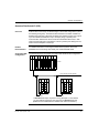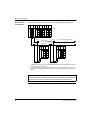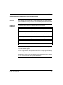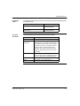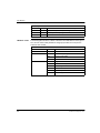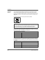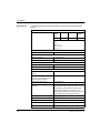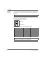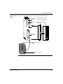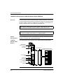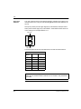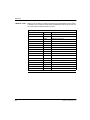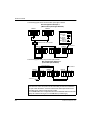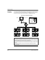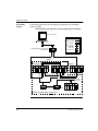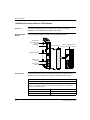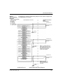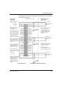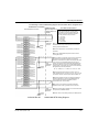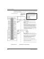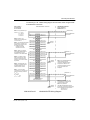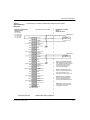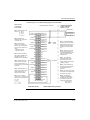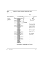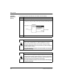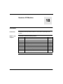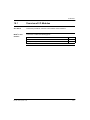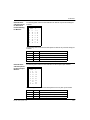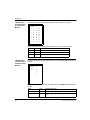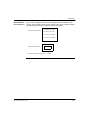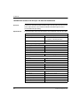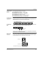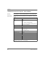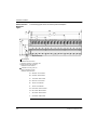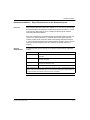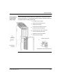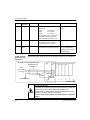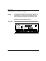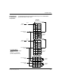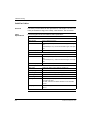
1
Modicon
Quantum Automation Series
Hardware Reference Guide
043505765 78
840 USE 100 00
Version 10.0
ii
Table of Contents
Safety Information . . . . . . . . . . . . . . . . . . . . . . . . . . . . . . . . . . . ix
About the Book . . . . . . . . . . . . . . . . . . . . . . . . . . . . . . . . . . . . . . xi
Part I Quantum Automation System Overview . . . . . . . . . . . . . 1
At a Glance . . . . . . . . . . . . . . . . . . . . . . . . . . . . . . . . . . . . . . . . . . . . . . . . . . . . . . 1
Chapter 1
Modicon TSX Quantum Automation System Overview . . . . . . 3
At a Glance . . . . . . . . . . . . . . . . . . . . . . . . . . . . . . . . . . . . . . . . . . . . . . . . . . . . . . 3
Modicon TSX Quantum Automation Series Overview. . . . . . . . . . . . . . . . . . . . . . 4
Quantum Power Supplies . . . . . . . . . . . . . . . . . . . . . . . . . . . . . . . . . . . . . . . . . . . 5
Quantum CPU Modules . . . . . . . . . . . . . . . . . . . . . . . . . . . . . . . . . . . . . . . . . . . . 6
Quantum I/O Modules . . . . . . . . . . . . . . . . . . . . . . . . . . . . . . . . . . . . . . . . . . . . . . 7
Quantum Communication Interface Modules . . . . . . . . . . . . . . . . . . . . . . . . . . . . 8
Quantum Intelligent/Special Purpose I/O Modules . . . . . . . . . . . . . . . . . . . . . . . 11
Quantum Simulator Modules (XSM) . . . . . . . . . . . . . . . . . . . . . . . . . . . . . . . . . . 12
Quantum Battery, Backplanes, and CableFast Cabling . . . . . . . . . . . . . . . . . . . 13
Quantum Programming Packages . . . . . . . . . . . . . . . . . . . . . . . . . . . . . . . . . . . 14
Part II Quantum System Configurations . . . . . . . . . . . . . . . . . . 15
At a Glance . . . . . . . . . . . . . . . . . . . . . . . . . . . . . . . . . . . . . . . . . . . . . . . . . . . . . 15
Chapter 2
Quantum Configurations . . . . . . . . . . . . . . . . . . . . . . . . . . . . . . 17
At a Glance . . . . . . . . . . . . . . . . . . . . . . . . . . . . . . . . . . . . . . . . . . . . . . . . . . . . .
Quantum Local I/O, Remote I/O and Distributed I/O Configurations. . . . . . . . . .
Quantum Local I/O . . . . . . . . . . . . . . . . . . . . . . . . . . . . . . . . . . . . . . . . . . . . . . .
Quantum Remote I/O (RIO) . . . . . . . . . . . . . . . . . . . . . . . . . . . . . . . . . . . . . . . .
Quantum Distributed I/O (DIO) . . . . . . . . . . . . . . . . . . . . . . . . . . . . . . . . . . . . . .
Chapter 3
17
18
20
21
25
Network Configurations . . . . . . . . . . . . . . . . . . . . . . . . . . . . . . . 29
At a Glance . . . . . . . . . . . . . . . . . . . . . . . . . . . . . . . . . . . . . . . . . . . . . . . . . . . . .
Quantum Network Support . . . . . . . . . . . . . . . . . . . . . . . . . . . . . . . . . . . . . . . . .
Quantum Network Interface Techniques. . . . . . . . . . . . . . . . . . . . . . . . . . . . . . .
Quantum Modbus and Modbus Plus Communications . . . . . . . . . . . . . . . . . . . .
29
30
33
37
iii
Part III Quantum System Specifications . . . . . . . . . . . . . . . . . . . 41
At a Glance . . . . . . . . . . . . . . . . . . . . . . . . . . . . . . . . . . . . . . . . . . . . . . . . . . . . . 41
Chapter 4
System Specifications for the Quantum Module . . . . . . . . . . 43
Quantum System Specifications . . . . . . . . . . . . . . . . . . . . . . . . . . . . . . . . . . . . . 43
Part IV Quantum Module Specifications and Configuration . . . 49
At a Glance . . . . . . . . . . . . . . . . . . . . . . . . . . . . . . . . . . . . . . . . . . . . . . . . . . . . . 49
Chapter 5
Hardware Specifications for the Quantum Modules. . . . . . . . 51
Quantum Hardware Specifications . . . . . . . . . . . . . . . . . . . . . . . . . . . . . . . . . . . 51
Chapter 6
Power Supply Modules . . . . . . . . . . . . . . . . . . . . . . . . . . . . . . . 61
At a Glance . . . . . . . . . . . . . . . . . . . . . . . . . . . . . . . . . . . . . . . . . . . . . . . . . . . . . 61
140CPS11100 AC Power Supply 115/230 Vac 3 A Module . . . . . . . . . . . . . . . . 62
140CPS11400 AC Power Supply, 115/230 Vac, 8 A Module . . . . . . . . . . . . . . . 65
140CPS11410 AC Summable Power Supply 115/230 Vac, 8 A . . . . . . . . . . . . . 68
140CPS11420 AC Summable Power Supply 115/230 Vac, 11 A . . . . . . . . . . . . 71
140CPS12400 AC Redundant Power Supply, 115/230 Vac 8 A Module . . . . . . 74
140CPS12420 AC Redundant Power Supply, 115/230 Vac 11 A Module . . . . . 77
140CPS21100 DC Power Supply, 24 Vdc, 3 A Module. . . . . . . . . . . . . . . . . . . . 80
140CPS21400 DC Summable Power Supply, 24 Vdc, 8 A Module. . . . . . . . . . . 83
140CPS22400 DC Redundant Power Supply, 24 Vdc, 8 A Module . . . . . . . . . . 86
140CPS41400 DC Summable Power Supply, 48 Vdc, 8 A Module. . . . . . . . . . . 89
140CPS42400 DC Redundant Power Supply, 48 Vdc, 8 A Module . . . . . . . . . . 92
140CPS51100 DC Power Supply, 125 Vdc, 3 A Module. . . . . . . . . . . . . . . . . . . 96
140CPS52400 DC Standalone/Redundant Power Supply, 125 Vdc, 8 A . . . . . . 99
Chapter 7
CPU Modules . . . . . . . . . . . . . . . . . . . . . . . . . . . . . . . . . . . . . . 103
At a Glance . . . . . . . . . . . . . . . . . . . . . . . . . . . . . . . . . . . . . . . . . . . . . . . . . . . . 103
140CPU11302 CPU Module . . . . . . . . . . . . . . . . . . . . . . . . . . . . . . . . . . . . . . . 105
140CPU11303 CPU Module . . . . . . . . . . . . . . . . . . . . . . . . . . . . . . . . . . . . . . . 115
140CPU21304 CPU Module . . . . . . . . . . . . . . . . . . . . . . . . . . . . . . . . . . . . . . . 125
140CPU42402 CPU Module . . . . . . . . . . . . . . . . . . . . . . . . . . . . . . . . . . . . . . . 135
140CPU43412 CPU Module . . . . . . . . . . . . . . . . . . . . . . . . . . . . . . . . . . . . . . . 145
140CPU43412A CPU Module . . . . . . . . . . . . . . . . . . . . . . . . . . . . . . . . . . . . . . 156
140CPU53414 CPU Module . . . . . . . . . . . . . . . . . . . . . . . . . . . . . . . . . . . . . . . 167
140CPU53414A CPU Module . . . . . . . . . . . . . . . . . . . . . . . . . . . . . . . . . . . . . . 178
Chapter 8
Quantum Field Bus Modules . . . . . . . . . . . . . . . . . . . . . . . . . 189
Overview . . . . . . . . . . . . . . . . . . . . . . . . . . . . . . . . . . . . . . . . . . . . . . . . . . . . . . 189
140CRP81100 Profibus DP Master Communications Module. . . . . . . . . . . . . . 190
140EIA92100 Quantum AS-i Master Module. . . . . . . . . . . . . . . . . . . . . . . . . . . 196
140NOA6XXXX Quantum InterBus Communications Modules . . . . . . . . . . . . . 201
140NOL911X0 Quantum LonWorks Network Option Modules . . . . . . . . . . . . . 208
iv
Chapter 9
Distributed I/O (DIO) for the Quantum Modules. . . . . . . . . . . 215
At a Glance . . . . . . . . . . . . . . . . . . . . . . . . . . . . . . . . . . . . . . . . . . . . . . . . . . . . 215
140CRA21X10 Quantum Distributed I/O (DIO) Modules . . . . . . . . . . . . . . . . . 216
140CRA21X20 Quantum Distributed I/O (DIO) Modules . . . . . . . . . . . . . . . . . 221
Chapter 10
Quantum Remote I/O Communication Modules . . . . . . . . . . 227
At a Glance . . . . . . . . . . . . . . . . . . . . . . . . . . . . . . . . . . . . . . . . . . . . . . . . . . . . 227
140CRP93X00 Remote I/O (RIO) Head Single and Dual Channel Module . . . 228
140CRA93X00 Quantum RIO Adapter Drop Single and Dual Channel Module 233
Chapter 11
Quantum Modbus Plus Network Option Modules . . . . . . . . . 239
140NOM21X00 Quantum Modbus Plus Network Option Modules . . . . . . . . . . 239
Chapter 12
Quantum Modbus Plus Networking on Fiber Module . . . . . . 249
140NOM25200 Quantum Networking Modbus Plus on Fiber Module . . . . . . . 249
Chapter 13
Quantum Ethernet Modules. . . . . . . . . . . . . . . . . . . . . . . . . . . 271
At a Glance . . . . . . . . . . . . . . . . . . . . . . . . . . . . . . . . . . . . . . . . . . . . . . . . . . . .
140NOE2X100 Quantum Ethernet TCP/IP Module . . . . . . . . . . . . . . . . . . . . .
140NOE3X100 Quantum Ethernet SY/MAX Modules. . . . . . . . . . . . . . . . . . . .
140NOE5X100 Quantum Ethernet MMS Modules . . . . . . . . . . . . . . . . . . . . . .
140NOE771xx Ethernet Modules . . . . . . . . . . . . . . . . . . . . . . . . . . . . . . . . . . .
Chapter 14
Intelligent/Special Purpose Modules for the Quantum . . . . . 297
At a Glance . . . . . . . . . . . . . . . . . . . . . . . . . . . . . . . . . . . . . . . . . . . . . . . . . . . .
140EHC10500 High Speed Counter Module . . . . . . . . . . . . . . . . . . . . . . . . . .
I/O Configuration for 140EHC20200 . . . . . . . . . . . . . . . . . . . . . . . . . . . . . . . . .
140EHC20200 High Speed Counter Module . . . . . . . . . . . . . . . . . . . . . . . . . .
140ESI06210 ASCII Interface Module . . . . . . . . . . . . . . . . . . . . . . . . . . . . . . .
140HLI34000 High Speed Interrupt Module . . . . . . . . . . . . . . . . . . . . . . . . . . .
140MSB/MSC10100 Quantum MSX Motion Modules. . . . . . . . . . . . . . . . . . . .
140XBE10000 Backplane Expander and Cable . . . . . . . . . . . . . . . . . . . . . . . .
140CHS11000 Hot Standby Module . . . . . . . . . . . . . . . . . . . . . . . . . . . . . . . . .
Chapter 15
15.1
15.2
15.3
271
272
276
279
282
297
298
304
333
346
352
357
368
372
Quantum Intrinsically Safe Analog/Digital, Input/Output
Modules . . . . . . . . . . . . . . . . . . . . . . . . . . . . . . . . . . . . . . . . . . . 375
At a Glance . . . . . . . . . . . . . . . . . . . . . . . . . . . . . . . . . . . . . . . . . . . . . . . . . . . .
Intrinsically Safe Modules - General Information. . . . . . . . . . . . . . . . . . . . . . . .
Intrinsically Safe Modules – General Description . . . . . . . . . . . . . . . . . . . . . . .
Intrinsically Safe Analog Modules . . . . . . . . . . . . . . . . . . . . . . . . . . . . . . . . . . .
At a Glance . . . . . . . . . . . . . . . . . . . . . . . . . . . . . . . . . . . . . . . . . . . . . . . . . . . .
I/O Configuration for Intrinsically Safe Analog Modules . . . . . . . . . . . . . . . . . .
140AII33000 Intrinsically Safe Analog Input Module. . . . . . . . . . . . . . . . . . . . .
140AII33010 Intrinsically Safe Current Input Module . . . . . . . . . . . . . . . . . . . .
140AIO33000 Intrinsically Safe Analog Output Module . . . . . . . . . . . . . . . . . .
Intrinsically Safe Discrete Modules . . . . . . . . . . . . . . . . . . . . . . . . . . . . . . . . . .
At a Glance . . . . . . . . . . . . . . . . . . . . . . . . . . . . . . . . . . . . . . . . . . . . . . . . . . . .
375
376
376
380
380
381
390
403
409
414
414
v
I/O Configuration for Intrinsically Safe Discrete Modules. . . . . . . . . . . . . . . . . . 415
140DII33000 Intrinsically Safe Discrete Input Module . . . . . . . . . . . . . . . . . . . . 417
140DIO33000 Intrinsically Safe Discrete Output Module. . . . . . . . . . . . . . . . . . 423
Chapter 16
Quantum Simulator Modules . . . . . . . . . . . . . . . . . . . . . . . . . 429
At a Glance . . . . . . . . . . . . . . . . . . . . . . . . . . . . . . . . . . . . . . . . . . . . . . . . . . . . 429
140XSM00200 Quantum Point Discrete Simulator Module . . . . . . . . . . . . . . . . 430
140XSM01000 Analog Simulator Module . . . . . . . . . . . . . . . . . . . . . . . . . . . . . 432
Chapter 17
Quantum Battery Module . . . . . . . . . . . . . . . . . . . . . . . . . . . . 437
At a Glance . . . . . . . . . . . . . . . . . . . . . . . . . . . . . . . . . . . . . . . . . . . . . . . . . . . . 437
I/O Configuration for the 140XCP90000 Battery Module . . . . . . . . . . . . . . . . . . 438
140XCP90000 Quantum Battery Module. . . . . . . . . . . . . . . . . . . . . . . . . . . . . . 439
Chapter 18
18.1
18.2
18.3
18.4
18.5
vi
Quantum I/O Modules . . . . . . . . . . . . . . . . . . . . . . . . . . . . . . . 445
At a Glance . . . . . . . . . . . . . . . . . . . . . . . . . . . . . . . . . . . . . . . . . . . . . . . . . . . . 445
Overview of I/O Modules . . . . . . . . . . . . . . . . . . . . . . . . . . . . . . . . . . . . . . . . . . 447
Overview of I/O Modules . . . . . . . . . . . . . . . . . . . . . . . . . . . . . . . . . . . . . . . . . . 447
Quantum I/O Modules . . . . . . . . . . . . . . . . . . . . . . . . . . . . . . . . . . . . . . . . . . . . 448
I/O Map Status Byte. . . . . . . . . . . . . . . . . . . . . . . . . . . . . . . . . . . . . . . . . . . . . . 459
Analog Input Modules . . . . . . . . . . . . . . . . . . . . . . . . . . . . . . . . . . . . . . . . . . . . 461
At a Glance . . . . . . . . . . . . . . . . . . . . . . . . . . . . . . . . . . . . . . . . . . . . . . . . . . . . 461
Analog Input Modules . . . . . . . . . . . . . . . . . . . . . . . . . . . . . . . . . . . . . . . . . . . . 462
140ACI03000 I/O Analog In Module . . . . . . . . . . . . . . . . . . . . . . . . . . . . . . . . . 479
140ACI04000 High Density Analog in I/O Module . . . . . . . . . . . . . . . . . . . . . . . 483
140ARI03010 I/O RTD Input 8 Channel Module . . . . . . . . . . . . . . . . . . . . . . . . 487
140ATI03000 I/O Thermocouple Input 8 Channel Module . . . . . . . . . . . . . . . . 491
140AVI03000 I/O Analog IN 8 Channel Bipolar Module . . . . . . . . . . . . . . . . . . 495
Analog Output Modules . . . . . . . . . . . . . . . . . . . . . . . . . . . . . . . . . . . . . . . . . . . 499
At a Glance . . . . . . . . . . . . . . . . . . . . . . . . . . . . . . . . . . . . . . . . . . . . . . . . . . . . 499
I/O Configuration for Analog Output Modules . . . . . . . . . . . . . . . . . . . . . . . . . . 500
140ACO02000 Quantum I/O Analog Current Out Module. . . . . . . . . . . . . . . . . 505
140ACO13000 High Density Analog Out I/O Module . . . . . . . . . . . . . . . . . . . . 509
140AVO02000 Quantum I/O Analog Voltage Out Module. . . . . . . . . . . . . . . . . 513
Analog Input/Output Modules . . . . . . . . . . . . . . . . . . . . . . . . . . . . . . . . . . . . . . 517
At a Glance . . . . . . . . . . . . . . . . . . . . . . . . . . . . . . . . . . . . . . . . . . . . . . . . . . . . 517
Configuration of the 140AMM09000 Analog Input/Output Module . . . . . . . . . . 518
140AMM09000 Analog Input/Output Module. . . . . . . . . . . . . . . . . . . . . . . . . . . 523
Discrete Input Modules . . . . . . . . . . . . . . . . . . . . . . . . . . . . . . . . . . . . . . . . . . . 529
At a Glance . . . . . . . . . . . . . . . . . . . . . . . . . . . . . . . . . . . . . . . . . . . . . . . . . . . . 529
I/O Configuration for Discrete Input Modules. . . . . . . . . . . . . . . . . . . . . . . . . . . 530
140DAI34000 Quantum I/O 24 VAC IN Module. . . . . . . . . . . . . . . . . . . . . . . . . 534
140DAI35300 Quantum I/O AC Input 24 Vac Module . . . . . . . . . . . . . . . . . . . . 537
140DAI44000 Quantum I/O 48 VAC IN Module. . . . . . . . . . . . . . . . . . . . . . . . . 540
140DAI45300 Quantum I/O AC Input 48 Vac 4x8 Module. . . . . . . . . . . . . . . . . 543
140DAI54000 Quantum I/O 115 VAC In Module . . . . . . . . . . . . . . . . . . . . . . . . 546
18.6
18.7
18.8
18.9
140DAI54300 Quantum I/O AC Input 115 Vac 2x8 Module . . . . . . . . . . . . . . . 549
140DAI55300 Quantum I/O AC Input 115 Vac 4x8 Module . . . . . . . . . . . . . . . 553
140DAI74000 Quantum I/O AC Input 230 Vac 16x1 Module . . . . . . . . . . . . . . 557
140DAI75300 Quantum I/O AC Input 230 Vac 4x8 Module . . . . . . . . . . . . . . . 560
140DDI15310 Quantum I/O DC Input 5 V TTL 4x8 Source Module . . . . . . . . . 563
140DDI35300 Quantum I/O DC Input 24 Vdc 4x8 Sink Module . . . . . . . . . . . . 566
140DDI35310 Quantum I/O DC Input 24 Vdc True Low 4x8 Input Module. . . . 568
140DDI36400 I/O DC Input 24 VDC 6x16 Telefast Input Module . . . . . . . . . . . 570
140DDI67300 Quantum I/O DC Input 125 Vdc 3x8 Sink Module . . . . . . . . . . . 574
140DDI84100 Quantum I/O DC Input 10 ... 60 Vdc 8x2 Sink Module. . . . . . . . 578
140DDI85300 Quantum I/O DC Input 10 ... 60 Vdc 4x8 Sink Module. . . . . . . . 581
Discrete Output Modules. . . . . . . . . . . . . . . . . . . . . . . . . . . . . . . . . . . . . . . . . . 584
At a Glance . . . . . . . . . . . . . . . . . . . . . . . . . . . . . . . . . . . . . . . . . . . . . . . . . . . . 584
I/O Configuration for Discrete Output Modules . . . . . . . . . . . . . . . . . . . . . . . . . 585
140DAO84000 I/O AC Output 24 ... 230 Vac 16x1 Module . . . . . . . . . . . . . . . 594
140DAO84010 I/O AC Output 24 ... 115 Vac 16x1 Module . . . . . . . . . . . . . . . 598
140DAO84210 Quantum I/O AC Output 100 ... 230 Vac 4x4 Module . . . . . . . 603
140DAO84220 Quantum I/O AC Output 24 ... 48 Vac 4x4 Module . . . . . . . . . 608
140DAO85300 Quantum I/O AC Output 24 ... 230 Vac 4x8 Module . . . . . . . . 613
140DDO15310 I/O DC Output 5 V TTL 4x8 Sink Module . . . . . . . . . . . . . . . . . 618
140DDO35300 Quantum I/O DC Output 24 Vdc 4x8 Source Module. . . . . . . . 622
140DDO35301 I/O DC Output 24 VDC 4x8 Discrete Source Module. . . . . . . . 627
140DDO35310 I/O DC Output 24 Vdc 4x8 Sink Module. . . . . . . . . . . . . . . . . . 631
140DDO36400 I/O DC Output 24VDC 6x16 Telefast Output Module. . . . . . . . 636
140DDO84300 Quantum I/O DC Output 10 ... 60 Vdc 2x8 Source Module . . . 641
140DDO88500 Quantum I/O DC Output 24-125 Vdc 2x6 Source Module . . . . 644
140DRA84000 Quantum I/O Relay Output 16x1 Normally Open Module. . . . . 649
140DRC83000 Quantum I/O Relay Output 8x1 Normally Open/Normally Closed
Module. . . . . . . . . . . . . . . . . . . . . . . . . . . . . . . . . . . . . . . . . . . . . . . . . . . . . . . . 652
Discrete Verified Output Module . . . . . . . . . . . . . . . . . . . . . . . . . . . . . . . . . . . . 655
At a Glance . . . . . . . . . . . . . . . . . . . . . . . . . . . . . . . . . . . . . . . . . . . . . . . . . . . . 655
I/O Configuration for the Discrete Verified Output Module – 140DVO85300 . . 656
140DVO85300 I/O Verified 10-30 VDC Out Module . . . . . . . . . . . . . . . . . . . . . 661
Discrete Supervised Input Module . . . . . . . . . . . . . . . . . . . . . . . . . . . . . . . . . . 665
At a Glance . . . . . . . . . . . . . . . . . . . . . . . . . . . . . . . . . . . . . . . . . . . . . . . . . . . . 665
I/O Configuration for the Discrete Supervised Input Module – 140DSI35300 . . 666
140DSI35300 I/O DC 24V Supervised Input Module . . . . . . . . . . . . . . . . . . . . 667
Discrete Input/Output Modules . . . . . . . . . . . . . . . . . . . . . . . . . . . . . . . . . . . . . 670
At a Glance . . . . . . . . . . . . . . . . . . . . . . . . . . . . . . . . . . . . . . . . . . . . . . . . . . . . 670
I/O Configuration for Discrete Input/Output Modules . . . . . . . . . . . . . . . . . . . . 671
140DAM59000 Quantum I/O AC Input 115 Vac 2x8 / AC Output 115 Vac 2x4) 676
140DDM39000 I/O DC Input 24 Vdc 2x8 Sink / DC Output 24 Vdc 2x4 Source
Module. . . . . . . . . . . . . . . . . . . . . . . . . . . . . . . . . . . . . . . . . . . . . . . . . . . . . . . . 682
140DDM69000 I/O 125 VDC Input/High Power Output Module . . . . . . . . . . . . 688
vii
Appendices
. . . . . . . . . . . . . . . . . . . . . . . . . . . . . . . . . . . . . . . . . . . . . . 695
At a Glance . . . . . . . . . . . . . . . . . . . . . . . . . . . . . . . . . . . . . . . . . . . . . . . . . . . . 695
Appendix A
Miscellaneous Components . . . . . . . . . . . . . . . . . . . . . . . . . . 697
Miscellaneous Components. . . . . . . . . . . . . . . . . . . . . . . . . . . . . . . . . . . . . . . . 697
Appendix B
Spare Parts . . . . . . . . . . . . . . . . . . . . . . . . . . . . . . . . . . . . . . . . 707
Spare Parts . . . . . . . . . . . . . . . . . . . . . . . . . . . . . . . . . . . . . . . . . . . . . . . . . . . . 707
Appendix C
Hardware Installation. . . . . . . . . . . . . . . . . . . . . . . . . . . . . . . . 709
At a Glance . . . . . . . . . . . . . . . . . . . . . . . . . . . . . . . . . . . . . . . . . . . . . . . . . . . . 709
Hardware Installation – Selecting Backplanes. . . . . . . . . . . . . . . . . . . . . . . . . . 710
Hardware Installation – Mounting Brackets . . . . . . . . . . . . . . . . . . . . . . . . . . . . 717
Hardware Installation – Space Requirements for the Quantum System . . . . . . 721
Hardware Installation – Mounting Quantum Modules . . . . . . . . . . . . . . . . . . . . 723
Appendix D
Power and Grounding Guidelines . . . . . . . . . . . . . . . . . . . . . 729
At a Glance . . . . . . . . . . . . . . . . . . . . . . . . . . . . . . . . . . . . . . . . . . . . . . . . . . . . 729
Power and Grounding Considerations for AC and DC Powered Systems. . . . . 730
System Design Considerations for Quantum Power Supplies. . . . . . . . . . . . . . 739
Grounding . . . . . . . . . . . . . . . . . . . . . . . . . . . . . . . . . . . . . . . . . . . . . . . . . . . . . 745
Closed System Installation. . . . . . . . . . . . . . . . . . . . . . . . . . . . . . . . . . . . . . . . . 747
Appendix E
CableFast Cabling . . . . . . . . . . . . . . . . . . . . . . . . . . . . . . . . . . 749
At a Glance . . . . . . . . . . . . . . . . . . . . . . . . . . . . . . . . . . . . . . . . . . . . . . . . . . . . 749
Features of the CableFast Cabling System . . . . . . . . . . . . . . . . . . . . . . . . . . . . 750
140CFA04000 CableFast Cabling Block . . . . . . . . . . . . . . . . . . . . . . . . . . . . . . 757
140CFB03200 Quantum CableFast Cabling Block . . . . . . . . . . . . . . . . . . . . . . 760
140CFC03200 Quantum CableFast Cabling Block . . . . . . . . . . . . . . . . . . . . . . 764
140CFD03200 Quantum CableFast Cabling Block . . . . . . . . . . . . . . . . . . . . . . 773
140CFE03200 Quantum CableFast Cabling Block . . . . . . . . . . . . . . . . . . . . . . 775
140CFG01600 Quantum CableFast Cabling Block . . . . . . . . . . . . . . . . . . . . . . 777
140CFH00800 Quantum CableFast Cabling Block . . . . . . . . . . . . . . . . . . . . . . 785
140CFI00800 Quantum CableFast Cabling Block . . . . . . . . . . . . . . . . . . . . . . . 793
140CFJ00400 Quantum CableFast Cabling Block . . . . . . . . . . . . . . . . . . . . . . 800
140CFK00400 Quantum CableFast Cabling Block . . . . . . . . . . . . . . . . . . . . . . 808
CableFast Cables . . . . . . . . . . . . . . . . . . . . . . . . . . . . . . . . . . . . . . . . . . . . . . . 816
CableFast Accessories . . . . . . . . . . . . . . . . . . . . . . . . . . . . . . . . . . . . . . . . . . . 821
Appendix F
Error Stopped Codes. . . . . . . . . . . . . . . . . . . . . . . . . . . . . . . . 823
Error Stopped Codes . . . . . . . . . . . . . . . . . . . . . . . . . . . . . . . . . . . . . . . . . . . . . 823
Appendix G
Agency Approvals . . . . . . . . . . . . . . . . . . . . . . . . . . . . . . . . . . 827
Agency Approvals . . . . . . . . . . . . . . . . . . . . . . . . . . . . . . . . . . . . . . . . . . . . . . . 827
Index
viii
. . . . . . . . . . . . . . . . . . . . . . . . . . . . . . . . . . . . . . . . . . . . . . xiii
Safety Information
§
Important Information
NOTICE
Read these instructions carefully, and look at the equipment to become familiar with
the device before trying to install, operate, or maintain it. The following special
messages may appear throughout this documentation or on the equipment to warn
of potential hazards or to call attention to information that clarifies or simplifies a
procedure.
The addition of this symbol to a Danger or Warning safety label indicates
that an electrical hazard exists, which will result in personal injury if the
instructions are not followed.
This is the safety alert symbol. It is used to alert you to potential personal
injury hazards. Obey all safety messages that follow this symbol to avoid
possible injury or death.
DANGER
DANGER indicates an imminently hazardous situation, which, if not avoided, will
result in death, serious injury, or equipment damage.
WARNING
WARNING indicates a potentially hazardous situation, which, if not avoided, can result
in death, serious injury, or equipment damage.
CAUTION
CAUTION indicates a potentially hazardous situation, which, if not avoided, can result
in injury or equipment damage.
840 USE 100 00 September 2002
ix
Safety Information
PLEASE NOTE
x
Electrical equipment should be serviced only by qualified personnel. No responsibility is assumed by Schneider Electric for any consequences arising out of the use
of this material. This document is not intended as an instruction manual for untrained
persons.
© 2002 Schneider Electric
All Rights Reserved
840 USE 100 00 September 2002
About the Book
At a Glance
Document Scope
This manual is a reference guide for the Hardware of the Quantum automation
system.
Validity Note
The data and illustrations found in this book are not binding. We reserve the right to
modify our products in line with our policy of continuous product development. The
information in this document is subject to change without notice and should not be
construed as a commitment by Schneider Electric.
Product Related
Warnings
Schneider Electric assumes no responsibility for any errors that may appear in this
document. If you have any suggestions for improvements or amendments or have
found errors in this publication, please notify us. No part of this document may be
reproduced in any form or by any means, electronic or mechanical, including
photocopying, without express written permission of Schneider Electric.
User Comments
We welcome your comments about this document. You can reach us by e-mail at
[email protected]
840 USE 100 00 September 2002
xi
About the Book
xii
840 USE 100 00 September 2002
Quantum Automation System
Overview
I
At a Glance
Overview
This part provides an overview of the Quantum Automation System.
What’s in this
Part?
This part contains the following chapters:
Chapter
1
840 USE 100 00 September 2002
Chapter Name
Modicon TSX Quantum Automation System Overview
Page
3
1
Quantum Overview
2
840 USE 100 00 September 2002
Modicon TSX Quantum
Automation System Overview
1
At a Glance
Introduction
This chapter provides an overview of the Quantum TSX Automation System, which
includes Quantum software support.
What’s in this
Chapter?
This chapter contains the following topics:
Topic
Modicon TSX Quantum Automation Series Overview
Page
4
Quantum Power Supplies
5
Quantum CPU Modules
6
Quantum I/O Modules
7
Quantum Communication Interface Modules
8
Quantum Intelligent/Special Purpose I/O Modules
11
Quantum Simulator Modules (XSM)
12
Quantum Battery, Backplanes, and CableFast Cabling
13
Quantum Programming Packages
14
840 USE 100 00 September 2002
3
Quantum Overview
Modicon TSX Quantum Automation Series Overview
Overview
The Quantum system is a special-purpose computing system with digital processing
capabilities. Quantum is designed for real time control in industrial and
manufacturing applications in a modular, expandable architecture employing the
following modules.
l
l
l
l
l
l
l
l
l
Quantum System
Block Diagram
Power Supply
CPU
I/O
I/O Network Interface
Intelligent/Special Purpose I/O
Simulator (XSM)
Battery
Backplanes
CableFast Cabling
The following figure is a block diagram of a typical Quantum system.
Local I/O Drop
P/S
CPU
Ethernet TCP/IP
RIO NOM NOE
Head
MB+
Tap
Modbus Plus DIO
Twisted Pair Cable
DIO Drop
DIO
Drop
I/O
4
I/O
I/O
I/O
I/O
Modbus Plus Cable
MB+
Tap
RIO Coaxial
I/O
P/S
MB+
Tap
I/O
RIO
Drop
RIO Drop
I/O
I/O
I/O
I/O
RIO
Tap
840 USE 100 00 September 2002
Quantum Overview
Quantum Power Supplies
Overview
Quantum power supplies are used to supply system power to all modules inserted
into the backplane, including:
l Quantum CPU modules
l Quantum Interface modules
l Quantum I/O modules
Depending upon the system configuration, the option exists of using the power
supply in three different modes.
Power Supply
Modes
The following table shows the power supply modes.
Power Supply Type
Usage
Standalone
For 3 A, 8 A or 11 A configurations that do not require fault
tolerant or redundant capabilities.
Standalone Summable
For configurations consuming more than the rated current of one
supply, two summing power supplies can be installed in the
same backplane.
Redundant
For configurations requiring power for uninterrupted system
operation. Two redundant power supplies are required for
redundancy.
CAUTION
System Safety
Exercise caution when considering a combination of power supplies in
a backplane. Use only like power supplies with the exceptions noted in
System Design Considerations for Quantum Power Supplies, p. 739.
Failure to follow this precaution can result in injury or equipment
damage.
840 USE 100 00 September 2002
5
Quantum Overview
Quantum CPU Modules
Overview
The Quantum CPU is a module residing on the Quantum local I/O backplane. The
CPU is a digitally operating electronic system, which uses a programmable memory
for the internal storage of user instructions. These instructions are used to
implement specific functions such as:
l
l
l
l
l
Logic
Process sequencing
Timing
Coupling
Arithmetic
These instructions allow control through digital and analog outputs, for various types
of machines and processes.
The Quantum CPU serves as a bus master controlling the local, remote, and
distributed I/O of the Quantum system.
6
840 USE 100 00 September 2002
Quantum Overview
Quantum I/O Modules
Overview
Quantum I/O modules are electrical signal converters that convert signals to and
from field devices to a signal level and format, which can be processed by the CPU,
such as:
l
l
l
l
l
Limit switches
Proximity switches
Temperature sensors
Solenoids
Valve actuators
All I/O modules are optically isolated to the bus, ensuring safe and trouble-free
operation. All I/O modules are also software configurable.
840 USE 100 00 September 2002
7
Quantum Overview
Quantum Communication Interface Modules
Overview
Nine types of communication interface modules are available and presented in the
table below, and are described in the following text.
Network
Interface
Modules
The following table shows the communication interface modules.
Type
Description
RIO
Single and dual channel Remote I/O interface modules (RIO heads and
drops) connected via a coaxial cable network.
DIO
Single and dual channel Distributed I/O interface modules connected via a
twisted pair Modbus Plus cable network.
NOM
Single and dual channel Network Option Modules (NOM) connected via a
twisted pair Modbus Plus cable network.
Fiber Optic
Modbus Plus
Modbus Plus on fiber module connected via a fiber optic Modbus Plus cable
network.
Ethernet TCP/ Single channel Ethernet TCP/IP interface module connected via a twisted
IP
pair or fiber optic cable network.
8
InterBus
InterBus Interface module connected via a twisted pair network.
SY/MAX
Ethernet
SY/MAX Ethernet module connected via a twisted pair or fiber optic cable
network.
LonWorks
LonWorks module connected via a twisted-pair network.
MMS
Ethernet
MMS Ethernet module connected via a fiber optic cable network.
Profibus
Profibus Master module connected via a Profibus RS-485 port.
AS-i
AS-i module connected via a two wire AS-i port.
840 USE 100 00 September 2002
Quantum Overview
RIO Modules
(CRA/CRP)
Quantum RIO head and drop modules use a S908-based networking I/O
configuration. Communication is done via single or dual coaxial cabling up to 15,000
feet away. This configuration supports a mix of the following product lines:
l SY/MAX
l 200 Series
l 500 Series
l 800 Series
l Quantum I/O
When Quantum RIO is required, the Quantum controller may support up to 31 RIO
drops. In an RIO configuration, an RIO head module is connected with coaxial cable
to RIO drop modules at each remote drop.
DIO Module
(CRA)
Quantum DIO is implemented over a Modbus Plus network. The CPU or NOMs
module may be the network head via their Modbus Plus ports.
Quantum DIO Modbus Plus drop adaptors are specifically designed to link Quantum
I/O modules to the head via twisted pair shielded cable (Modbus Plus). The DIO
drop modules also provide the I/O with power (maximum 3A) from a 24 Vdc or a 115/
230 Vac source. Each DIO network supports up to 63 distributed drops using
repeaters.
Network Option
Module (NOM)
Quantum NOM modules provide extended communication capabilities for the
Quantum system within a Modbus Plus configuration.
Modbus Plus on
Fiber Module
(NOM)
Quantum Modbus Plus on Fiber modules provides connectivity to Modbus Plus
nodes by fiber cable without fiber optic repeaters, and allows the creation of a pure
fiber optic network or a mixed fiber optic/twisted-pair network (with the use of a
490NRP254 Fiber Optic Repeater).
Ethernet TCP/IP
(NOE) Modules
Quantum Ethernet TCP/IP modules make it possible for a Quantum controller to
communicate with devices on an Ethernet network using TCP/IP – the de facto
standard protocol. An Ethernet module may be inserted into an existing Quantum
system and connected to existing Ethernet networks via fiber optic or twisted pair
cabling.
SY/MAX Ethernet
Modules (NOE)
Quantum-SY/MAX-Ethernet modules are Quantum CPU network option modules
that can be placed in a Quantum backplane to connect Quantum controllers to SY/
MAX devices and applications.
840 USE 100 00 September 2002
9
Quantum Overview
MMS-Ethernet
Modules (NOE)
Quantum-MMS-Ethernet modules are Quantum CPU network option modules that
can be placed in a Quantum backplane to connect Quantum controllers to MMS
devices and applications.
InterBus
Interface Module
(NOA)
The Quantum InterBus is the interface module to the InterBus bus. The InterBus bus
is a fieldbus network designed for I/O blocks and intelligent devices used in
manufacturing. It offers a master/slave topology that permits deterministic I/O
servicing over it’s 13 km twisted pair network.
LonWorks
Modules (NOL)
Quantum NOL modules provide connectivity between a Quantum controller and a
LonWorks network, based on Echelon’s LonWorks technology. The NOL module is
offered in three models for different transceiver types, and supports three twistedpair media types with different network topologies or data transfer speeds.
Profibus
Interface Module
(CRP)
Quantum Profibus module is the interface module to Profibus-DP networks. The
interface modules use Type A, shielded twisted pair to join inline connectors, with or
without service ports and bus terminators.
AS-i Interface
Module
Quantum AS-i modules provide connectivity between a Quantum controller and
AS-i networks. AS-i bus cable is an unshielded flat two-wire link on which
communication and power are transmitted to connected devices. The media
insulation is self-healing to accommodate junction block removal.
10
840 USE 100 00 September 2002
Quantum Overview
Quantum Intelligent/Special Purpose I/O Modules
Overview
Quantum Intelligent/Special Purpose I/O modules operate with minimum
intervention from the Quantum controller after initially downloading module
parameters or programs. The Quantum intelligent/special purpose I/O modules
include the following.
l
l
l
l
l
840 USE 100 00 September 2002
High Speed Counter modules (EHC)
ASCII Interface module (ESI)
High Speed Interrupt module (HLI)
Single Axis Motion Modules (MSx)
Multi-Axis Motion Modules (MMS)
11
Quantum Overview
Quantum Simulator Modules (XSM)
Overview
There are two types of simulator modules, as described below.
Discrete and
Analog
Simulators
The following table shows discrete and analog simulators.
12
Type
Description
Discrete 16 Point
Simulator
(140XSM01000)
The Discrete Simulator (16 points) is used to generate up to 16 binary
input signals to the 140DAI54000 and the 140DAI74000 AC input
modules.
Analog Simulator
(140XSM01000)
The Analog Simulator (2 channels in, 1 channel out) module is used
for simulating 4 ... 20 mA field current loops used with current input
Quantum modules.
840 USE 100 00 September 2002
Quantum Overview
Quantum Battery, Backplanes, and CableFast Cabling
Battery Module
(XCP)
The Quantum battery module provides RAM backup power for the Quantum expert
module.
Backplanes
(XBP)
Quantum backplanes may be used in all locations of local, remote, or distributed I/
O. There are six backplanes available in 2, 3, 4, 6, 10, and 16 slot versions. All I/O
slots are usable with any module able to be used in any slot.
CableFast
Cabling
The Quantum CableFast wiring system consists of pre-wired Quantum field wiring
terminal strips and DIN rail-mounted terminal blocks, offered in straight through or
special application versions.
840 USE 100 00 September 2002
13
Quantum Overview
Quantum Programming Packages
Overview
Quantum controllers support several editors.
Quantum Editors
The following table shows the editors for the Quantum controllers.
14
Editor
Where Discussed
Modsoft V2.6
For more information on Modsoft, refer to the Modicon
Modsoft Programmer User Manual (890USE11500).
Concept V2.5
For more information on Concept, refer to the Concept User
Manual (840USE49300).
ProWORX NxT V2.1
For more information on ProWorX, refer to the ProWorX User
Manual (372SPU68001 NMAN)
ProWORX 32 (V 1.0
minimum)
For more information on ProWORX 32, refer to the ProWORX
32 Programming Software for PLCs User Guide (372SPU780
01EMAN)
ProWORX Plus (V 1.0
minimum)
For more information on ProWORX Plus, refer to the
ProWORX Plus for Modicon Reference Manual
(371SPU68001 PMAN).
Modicon State Language
(V1.2 minimum)
For more information on Modicon State Language, refer to the
Modicon State Language User Manual (GM-MSL1-001).
840 USE 100 00 September 2002
Quantum System Configurations
II
At a Glance
Overview
This part provides information on Quantum system configurations.
What’s in this
Part?
This part contains the following chapters:
Chapter
840 USE 100 00 September 2002
Chapter Name
Page
2
Quantum Configurations
17
3
Network Configurations
29
15
Quantum Configurations
16
840 USE 100 00 September 2002
Quantum Configurations
2
At a Glance
Introduction
The following chapter provides information on the Quantum configurations,
including Local I/O, Remote I/O (RIO), and Distributed I/O (DIO).
What’s in this
Chapter?
This chapter contains the following topics:
Topic
Quantum Local I/O, Remote I/O and Distributed I/O Configurations
Page
18
Quantum Local I/O
20
Quantum Remote I/O (RIO)
21
Quantum Distributed I/O (DIO)
25
840 USE 100 00 September 2002
17
Quantum Configurations
Quantum Local I/O, Remote I/O and Distributed I/O Configurations
Overview
The following information contains a description of the Local I/O, Remote I/O and
Distributed I/O and their configurations.
These configurations (see the configuration table below for valid Quantum
configurations) can be equipped with a combination of:
l Quantum CPUs
l Power supplies
l I/O interfaces
l Expert modules
l I/O modules
Note: Refer to System Specifications for the Quantum Module, p. 43 for a
complete list of part numbers for all Quantum modules.
Local, RIO, and
DIO
Configuration
The following table provides valid Quantum configurations, including backplanes
and modules.
If Configuration Backplane
Type Is
Types (Typical)
Are
Required
Modules Are
Optional
Modules Are
Modules Not
Permitted Are
Local
6, 10, 16 slots
Power Supply
CPU
RIO Head, I/O,
NOx*
RIO Drop, DIO
Drop
RIO**
6, 10, 16 slots
Power Supply
RIO Drop
I/O
CPU, RIO Head,
DIO Drop NOx*
DIO
2, 3, 4, 6 slots
DIO Drop
Power Supply,
I/O
CPU, RIO Head,
RIO Drop NOx*
*NOM, NOA, and NOE.
**Remote I/O is typically used for large (number of modules) drops 6, 10, or 16 slot
backplanes. Distributed I/O is typically used for small drops using 2, 3, 4, or 6 slot backplanes.
Note: Every Quantum module requires power from the backplane (except power
supply and DIO modules). For a valid configuration, add up the required backplane
current (in mA) for every module, and ensure that this number is less than the
available power in the selected power supply.
18
840 USE 100 00 September 2002
Quantum Configurations
Local, Remote
and Distributed
I/O Configuration
Depending on the type of configuration—Local, Remote, or Distributed I/O, a variety
of features will apply, as shown in the following table.
Feature
Configuration
Local I/O
Remote I/O
Distributed I/O
Maximum I/O Words
Per drop
64 in / 64 out
64 in / 64 out
30 in / 32 out
1,984 in / 1,984 out
500 in / 500 out
*864 any mix
448 any mix
Maximum drops per
network
31
63
Media
Coax
Twisted Pair
Speed
1.5 Mhz
1 MHz
Maximum distance
without repeaters
15,000 ft. (4,573 m)
1,500 ft. (457 m)
Scan synched I/O
servicing
Yes
No
Momentum I/O
support
No
Yes
Hot Standby
support
Yes
No
Modbus Plus
compatible
No
Yes
Per network
Maximum Physical Discretes
Per drop
*864 any mix
*Requires use of backplane expander, Telefast module excepted (27 modules x 32
points = 864). May be limited by bus power requirements.
840 USE 100 00 September 2002
19
Quantum Configurations
Quantum Local I/O
Overview
A local I/O configuration is contained in one rack and includes all Quantum modules
mounted in a standard Quantum backplane. Quantum Local I/O can be as few as
one I/O module (in a three slot backplane), or as many as 14, along with a CPU and
power supply in a single 16 slot backplane.
If required for the application, system interface modules are also included in the
Local I/O backplane. These modules could consist of one RIO processor or network
option modules.
I/O Configuration
The following figure is an example of a typical local I/O configuration.
PS CPU I/O I/O I/O I/O I/O I/O I/O I/O I/O I/O I/O I/O I/O I/O
2 Slot
3 Slot
4 Slot
6 Slot
10 Slot
16 Slot
Note: A maximum of 448 digital I/O points (14, 4x8 digital I/O modules), or a
maximum of 48 analog input channels (six 8-channel analog in modules) and 32
analog output channels (eight 4-channel analog out modules) may be serviced in
a single local I/O rack.
20
840 USE 100 00 September 2002
Quantum Configurations
Quantum Remote I/O (RIO)
Overview
Quantum RIO can be set up in single or dual cable configurations (refer to the
following two figures) and is contained in one rack at each RIO drop. When RIO is
used, the Quantum CPU may support several drops (a drop can be either Quantum,
SY/MAX, 200, 500, or 800 Series I/O systems).
Note: As stated above, the Quantum provides connectivity to other Modicon I/O
products via the same system. It will connect to 800 series I/O via the J890, J892,
P890, or P892 remote I/O adapters; 200 series I/O via J290 and J291 remote I/O
adapters; 500 series I/O via 29X/J540 remote I/O adapters; and SY/MAX
8030CRM931
Related
Documentation
For more information on use and installation of Quantum RIO, see Modicon Remote
I/O Cable System Planning and Installation Guide, Part Number 890USE10100
For more information on Hot Standby systems, see the Quantum Hot Standby
Installation and Planning Guide, Part Number 840USE10600.
Single Cable RIO
Configuration
The following figure is an example of a single cable Quantum RIO configuration.
RIO
PS CPU Head I/O I/O I/O
Local I/O
Drop
Up to 31 Drops
Terminator
RIO Tap
RIO Tap
RIO
PS Drop I/O I/O I/O I/O
RIO Drop # m
RIO Tap
RIO
PS Drop I/O I/O I/O I/O
P81
RIO Drop # n
J890
B800 Series Drop
*A RIO tap is required for every RIO drop in the system.
840 USE 100 00 September 2002
21
Quantum Configurations
Dual Cable RIO
Configuration
The following figure is an example of a dual cable Quantum RIO configuration.
RIO
PS CPUHead I/O I/O I/O
Local I/O
Drop
Up to 31 Drops
*RIO
Tap
*RIO
*RIO
Tap
*RIO Tap and
Terminator (#52-0422-000)
*RIO Tap
RIO
PSDrop I/O I/O I/O I/O
RIO Drop # m
*RIO Tap and
Terminator
RIO
PS Drop I/O I/O I/O
RIO Drop # n
P81
J890
B800 Series
*An RIO tap (# MA-0185-100) is required for every RIO drop in the system.
Note: The dual cable option is provided for systems that require added protection
against cable breaks or damaged connectors. With two cables connected between
the host and each node, no single cable break will disrupt communications.
Hot Standby
System
22
The Quantum Hot Standby system is designed for use with remote I/O networks. A
Quantum Hot Standby system may be set-up using single or dual cable
configurations (refer to the following two figures).
840 USE 100 00 September 2002
Quantum Configurations
Single Cable Hot
Standby
Configuration
The following figure is an example of a single cable Quantum Hot Standby
configuration.
Primary Controller
PS PLC RIO CHS
Standby Controller
PS PLC RIO CHS
Fiber Optic Cable
Self-terminating
F adapter
Self-terminating F adapter
#52-0411-000
(for quad shield cable)
#52-0399-000
(for non-quad shield cable)
Coaxial Cable
Splitter
#MA-0186-100
RIO Drop # 2
PS
RIO
I/O
I/O
I/O
Trunk
Cable
Last RIO Drop
Tap
#MA-0185-100
Trunk Terminator
#52-0422-000
840 USE 100 00 September 2002
PS
RIO
I/O
I/O
I/O
Tap
23
Quantum Configurations
Dual Cable Hot
Standby
Configuration
The following figure is an example of a dual cable Quantum Hot Standby
configuration.
Primary PLC
PS
Standby PLC
PLC RIO CHS
PS
PLC RIO CHS
Fiber Optic Cable
Self-terminating
F adapters
Coaxial Cable
Coaxial Cable
Splitter
#MA-0186-100
PS
RIO Drop # 2
RIO I/O I/O
I/O
Trunk
Line
A
Drop Cable
Trunk Terminator
#52-0422-000
Trunk Terminator
#52-0422-000
24
Splitter #MA-0186-100
Self-terminating F
adapters
#52-0411-000
(for quad shield cable)
#52-0399-000
(for non-quad shield
cable)
Trunk
Line
B
Tap
#MA-0185-100
PS
Last RIO Drop
RIO I/O I/O
I/O
Drop Cable
840 USE 100 00 September 2002
Quantum Configurations
Quantum Distributed I/O (DIO)
Overview
Quantum DIO can be set up in standard single or dual cable configurations (refer to
the following two figures). The Quantum DIO architecture is based on Modicon’s
Modbus Plus technology. When DIO is utilized, the Quantum system may support
up to three distributed networks of up to 64 drops (using a repeater) each.
Communication between the various nodes and the Modbus Plus head, in both
single and dual cable DIO configurations, is done by twisted pair cabling from the
head to the DIO adapters at the drops.
Related
Documentation
For detailed information concerning the Quantum DIO systems, refer to the
MODBUS Plus I/O Servicing User Guide, part number 840USE10400.
Single Cable DIO
Configuration
The following figure is an example of a single cable Quantum DIO configuration.
PS CPU I/O
I/O
I/O
I/O
I/O
I/O
I/O
I/O
Local I/O
Up to 31 drops (64 with repeater)
* Tap
* Tap
DIO I/O
Drop
I/O
I/O
Quantum Drop # m
** Drop Cable
DIO I/O
Drop
I/O
I/O
Quantum Drop # n
** Drop Cable
* A MODBUS Plus tap is required for every participant on the network.
** A drop cable is required for each drop from the MODBUS Plus tap.
(Cables are not included with the modules and need to be ordered.)
840 USE 100 00 September 2002
25
Quantum Configurations
Dual Cable DIO
Configuration
The following figure is an example of a dual cable Quantum DIO configuration.
PS CPU NOM I/O I/O I/O I/O I/O I/O I/O
Local I/O
*Tap
*Tap
Trunk Cable
*Tap
Trunk Cable
Up to 31 Nodes (63 with repeater)
*Tap
DIO I/O I/O I/O
Drop
Up to 31 Nodes (63 with repeater)
DIO I/O I/O I/O
Drop
Quantum Drop # n
Quantum Drop # m
***Drop Cables
***Drop Cables
*A MODBUS Plus tap (plastic, Part # 990NAD23000; ruggedized, Part # 990NAD23010) is required
for every participant on the network.
***A drop cable (8 ft/2.4 m, Part # 990NAD21110; 20 ft/6 m, Part # 990NAD21130) is required for
each drop from the MODBUS Plus tap. Cables are not included with the modules and need to be
ordered.
Note: The dual cable option is provided for systems that require added protection
against cable breaks or damaged connectors. With two cables connected between
the host and each node, no single cable break will disrupt communications.
26
840 USE 100 00 September 2002
Quantum Configurations
Part Numbers
MODBUS Plus taps that can be used for single and dual cable DIO configurations
include:
l Part Number 990NAD23000, plastic; and
l Part Number 990NAD23010, ruggedized.
The following MODBUS Plus trunk cables can be used with these DIO
configurations:
l Part Number 490NAA27101 (100 ft/30 m)
l Part Number 490NAA27102 (500 ft/152 m)
l Part Number 490NAA27103 (1000 ft/304 m)
l Part Number 490NAA27104 (1500 ft/456 m)
l Part Number 490NAA27105 (5000 ft/1520 m)
Drop cables that can be used for these configurations include:
l Part Number 990NAD21110 (8 ft/2.4 m)
l Part Number 990NAD21130 (20 ft/6 m)
840 USE 100 00 September 2002
27
Quantum Configurations
28
840 USE 100 00 September 2002
Network Configurations
3
At a Glance
Introduction
The following chapter provides information on the Quantum network support,
network interface techniques, and Modbus and Modbus Plus communications.
What’s in this
Chapter?
This chapter contains the following topics:
Topic
Page
Quantum Network Support
30
Quantum Network Interface Techniques
33
Quantum Modbus and Modbus Plus Communications
37
840 USE 100 00 September 2002
29
Network Configurations
Quantum Network Support
Overview
Quantum systems provide multiple choices for open, standards-based networking
and fieldbus connectivity requirements. The Quantum supported networks include:
l
l
l
l
l
l
l
l
l
Modbus
Modbus Plus
Remote I/O
TCP/IP Ethernet
SY/MAX Ethernet
MMS Ethernet
Interbus
LonWorks
SERCOS
Combinations of these networks can be used to provide simple, high performance
communication architectures which meet the tightly integrated needs of computer
and controller connectivity. A summary of the services available on these networks
is shown in the following table.
30
840 USE 100 00 September 2002
Network Configurations
Quantum
Supported
Networks
The following table shows the Quantum supported networks.
Service
Description
Modbus Modbus Remote Ethernet
Plus
I/O
TCP/ SY/
MMS
IP
MAX
Interbus
LonWorks SERCOS Profibus
Native to
Quantum
CPU
Y
Y
N
N
N
N
N
N
N
Available on a Y
Network
Module
Y
Y
Y
Y
Y
Y
Y
Y
Y
N
Y
N
N
N
N
N
N
N
N
N
N
N
N
N
N
Y
Y
Y
Y
Y
N
Y
Y
Y
N
Y
Y
N
N
N
N
N
N
N
N
N
N
N
N
Y
N
N
N
N
N
Y
Y
1
N
N
N
N
Y
Y
N
N
1
Y
N
N
N
N
N
N
N
CPU
Programming
CPU
Executive
Firmware
Loading
Support
Module
Firmware
Loaded From
CPU
Y
Y
1
1
Y
Report By
2
yY
Exception
Communications
Multi-node
Broadcast
Communications
N
Synchronized N
I/O Scanning
NonSynchronized I/O
Scanning
N
Quantum I/O
Drops
N
840 USE 100 00 September 2002
Y
Y
1
1
N
Y
Y
N
Y
Y
5
N
5
6
31
Network Configurations
Service
Description
Modbus Modbus Remote Ethernet
Plus
I/O
TCP/ SY/
MMS
IP
MAX
Interbus
LonWorks SERCOS Profibus
Hot Standby
Quantum I/O
Drop Support
N
N
Y
N
N
N
N
N
N
N
Hot Standby
Data
Communications Support
Y
Y
N
Y
N
N
N
N
N
N
Optional Dual N
Cabling
Y
1
Y
N
N
N
N
N
N
N
1
Y
Y
Y
1
N
N
N
N
1
N
N
N
N
1
N
N
N
N
1
Y
N
N
N
1
N
Y
Y
Optional
Fiber Optics
Momentum
I/O Drops
Variable
Speed Drives
Servo Motion
Control
Y
3
N
Y
N
Y
Y
3
Y
Y
HMI: Displays Y
& Panels
Y
HMI: Workstations
Y
Y
Y
Y
5
Y
3
Y
Y
Y
Y
3, 5
N
Y
4
N
3
3
3
Y
Y
Y
Y
Y
4
N
N
Y
4
N
Y
4
Y
Y
4
N
N
4
N
N
1. Refer to the Modbus Plus portion of the Quantum Specifier’s guide section for details of available services on
140NOM2XXX00 Modbus Plus Network modules
2. Service is only available on the native controller Modbus port when the XMIT loadable is used.
3. Available from third parties.
4. The SERCOS network standard is fiber optics.
5. The software for this module is a modConnect product.
6. Module firmware loaded through serial port on module.
32
840 USE 100 00 September 2002
Network Configurations
Quantum Network Interface Techniques
Overview
Quantum communication and networking modules use a variety of different
techniques to interface to the Quantum controller over the local backplane.
Direct CPU
Driver
This technique allows the CPU to control high speed data transfers to and from the
communication and networking modules, maximizing throughput and performance.
This technique is used extensively by the Remote I/O network and Hot Standby
system to ensure highly deterministic synchronization of the CPU and I/O scans.
Note: Only one Remote I/O Head Interface is supported for each Quantum CPU.
Option Module
Interface
This technique allows the communication and networking modules to control data
transfers to and from the CPU, maximizing the flexibility of the communications
interface.
This technique is used extensively by the Modbus Plus and Ethernet peer-to-peer
network modules. The number of option module interfaces supported by each CPU
model is described in the following table.
CPU Interface
Support
The following table shows the summary of Quantum CPU option module interface
support in standalone configurations.
Quantum Controller Model
Number
Available Option Module
Interfaces Supported Per CPU
140CPU53414(A)
6
140CPU43412(A)
6
140CPU42402
6
140CPU21304
2
140CPU11303
2
140CPU11302
2
Note: Refer to Quantum Modbus and Modbus Plus Communications, p. 37 for
details of available services on 140NOM2XX00 Modbus Plus Network modules.
840 USE 100 00 September 2002
33
Network Configurations
I/O Map Interface
Some network and communication modules are interfaced to the controller through
the standard I/O map configuration tables. In the following table, note that some
network and communication modules require a Loadable instruction which
enhances the standard controller Executive to support certain unique features of
individual modules.
In addition, some loadables allow the communication and networking modules to be
controlled by means of user-application code. The number of loadables and
associated modules that can be handled by an individual CPU depends upon its
memory size, the size of the application program, and the size of the loadables.
34
840 USE 100 00 September 2002
Network Configurations
Communications
and Networking
Model Number
The following table shows the Quantum communications and networking modules.
Description
Module
Interface
Technique
Loadable
Required
Backplane Support
Local
RIO
DIO
Bus Power mA
140CRP81100
Profibus
Direct CPU
Driver
N
Y
N
N
1200
140CRP93100
Remote I/O
Head Interface,
single cable
Direct CPU
Driver
N
Y
N
N
780
140CRP93200
Remote I/O
Head Interface,
dual cable
Direct CPU
Driver
N
Y
N
N
780
140CHS21000
Hot Standby
Processor Kit
Direct CPU
Driver
Y
Y
N
N
700
140NOA61110
Interbus Master
Direct CPU
Driver
Y
Y
N
N
700
140NOM21100
Modbus Plus
Options, single
cable
Option
Module
N
Y
N
N
780
140NOM21200
Modbus Plus
Option, dual
cable
Option
Module
N
Y
N
N
780
140NOM25200
Modbus Plus
Option, single
channel fiber
Option
Module
N
Y
N
N
900
140NOE21100
Ethernet TCP/IP
Twisted Pair
Option
Module
N
Y
N
N
1000
140NOE25100
Ethernet TCP/IP
Fiber Optic
Option
Module
N
Y
N
N
1000
140NOE31100
Ethernet SY/
MAX Twisted
Pair
Option
Module
N
Y
N
N
1000
140NOE35100
Ethernet SY/
MAX Fiber Optic
Option
Module
N
Y
N
N
1000
Ethernet MMS
Twisted Pair
Option
Module
N
Y
N
N
1000
Ethernet MMS
Fiber Optic
Option
Module
N
Y
N
N
1000
140NOE510 0
1
140NOE5510 0
1
840 USE 100 00 September 2002
35
Network Configurations
Model Number
Description
Module
Interface
Technique
Loadable
Required
Backplane Support
Bus Power mA
Local
RIO
DIO
140NOE77100/1
Ethernet TCP/IP
10/100 TX/FX
N
N
Y
N
N
750
140NOE77110/1
Ethernet TCP/IP
10/100 TX/FX
Factory Cast
N
N
Y
N
N
750
140MMS42500
Multi-Axis Motion Option
Controller w/
Module
SERCOS
N
Y
N
N
2500
140NOL91100
LonWorks
I/O Map (16/ Y
Interface, twisted 16)
pair FTT10
Y
Y
N
950
140NOL91110
LonWorks
I/O Map (16/ Y
Interface, twisted 16)
pair TPT/XF-78
Y
Y
N
950
140NOL91120
LonWorks
I/O Map (16/ Y
Interface, twisted 16)
pair TPT/XF1250
Y
Y
N
950
1. The software for this module is a ModConnect product.
36
840 USE 100 00 September 2002
Network Configurations
Quantum Modbus and Modbus Plus Communications
Overview
Each Quantum CPU includes both a Modbus and Modbus Plus communications
port. The features offered by both these communication protocols are listed in the
following table.
Modbus and
Modbus Plus
Features
The following table shows the Modbus and Modbus Plus features.
Modbus
Features
Modbus
Modbus Plus
Technique
Slaves polled by a master
Peer-to-peer, token rotation
Speed
19.2K typical
1M
Electrical
RS-232, various others
RS-485
Distance without repeater
RS-232, 50 ft. (15 m)
1,500 ft. (457 m)
Media
Various
Twisted pair, Fiber optics
Max nodes per network
247
64
Max network traffic
300 registers/sec @ 9.6 Kb
20,000 registers/sec
Programming
Yes
Yes
Read/Write data
Yes
Yes
Global data
No
Yes
Peer Cop
No
Yes
Modbus, a master/slave protocol, is a de facto industry standard with support from
over 500 industrial suppliers.
On-line programming or data acquisition applications are easily supported directly
from the serial port of any computer.
Modbus can be used in either a simple point-to-point manner with a pair of devices,
or in a network architecture with up to 247 slave devices.
840 USE 100 00 September 2002
37
Network Configurations
Modbus Plus
Modbus Plus combines high speed, peer-to-peer communication and easy
installation to simplify applications and reduce installation costs.
It allows host computers, controllers and other data sources to communicate as
peers throughout the network via low-cost twisted pair cable or optional fiber optic
cable.
As a deterministic token-passing network, Modbus Plus communicates at one
megabaud for fast access to process data. It’s strength is its ability to control realtime control devices like I/O and drives, without degraded performance due to
loading or traffic.
Bridging between Modbus and Modbus Plus is done automatically on CPUs and
Modbus Plus network modules.
The bridge mode redirects Modbus messages onto the Modbus Plus network for
easy connectivity between Modbus and Modbus Plus devices.
A summary of the available services on Quantum Modbus and Modbus Plus ports
is given in the following table.
38
840 USE 100 00 September 2002
Network Configurations
Modbus and
Modbus Plus
Services
Type
Modbus
Services
The following table shows the Quantum Modbus and Modbus Plus services.
Service Description
Native CPU Ports
NOM 1-2 Ports
NOM 3-6 Ports
Modbus
Modbus
Plus
Modbus
Modbus
Plus
Modbus
Modbus
Plus
Default Modbus Port Parameters Y
-
Y
-
Y
-
Configurable Modbus Port
Parameters
Y
-
Y
-
Modbus to Modbus Plus Bridging
Y
Local CPU Programming
Modbus
Plus
Services
2
-
4
-
4
-
Y
Y
Y
Y
3
-
4
-
N
4
-
Y
Y
5
-
3
-
2
Remote CPU Programming over
Modbus Plus
Y
Modbus access to local CPU
Y
-
Y
-
N
-
Modbus access to remote CPU
over Modbus Plus
Y
-
Y
-
Y
-
Y
-
Modbus Network Slave Support
Y
-
N
-
N
-
Modbus Master support with
XMIT Loadable
Y
-
N
-
N
-
Executive Firmware Loading
Support
Y
-
N
-
N
-
MSTR read/write register
-
Y
-
Y
-
Y
MSTR read/write Global Data
messaging
-
Y
-
Y
-
Y
MSTR get/clear local/remote
statistics
-
Y
-
Y
-
Y
Config Extension Global Data
Support
-
Y
-
Y
-
N
Config Extension Peer Cop
Support
-
Y
-
Y
-
N
Distributed I/O Support
-
Y
-
Y
-
N
CPU Programming
-
Executive Firmware Loading
Support
-
messagin g
6
840 USE 100 00 September 2002
Y
Y
4
-
Y
N
4
-
Y
4
N
39
Network Configurations
Note:
1. Only supported on the 140CPU42402, 140CPU42412(A) and 140CPU53414(A)
Quantum Controllers.
2. The native CPU Modbus port can be disabled from bridge mode operation with
the native Modbus Plus Port.
3. Modbus ports on NOMs are always in bridge mode with their associated
Modbus Plus port.
4. Only one programmer connection can be logged in at a time to any CPU, and
only one program monitor can be attached at a time to any CPU.
5. Modbus port parameters on NOMs 3-6 are defined by Modbus Port 3 in Concept
and Modsoft when the comm parameter selector switch is in mem.
6. Up to 4 MSTR read/write register instructions can be serviced per CPU scan per
Modbus Plus port.
40
840 USE 100 00 September 2002
Quantum System Specifications
III
At a Glance
Overview
This part provides system specifications for the Quantum automation system.
What’s in this
Part?
This part contains the following chapters:
Chapter
4
840 USE 100 00 September 2002
Chapter Name
System Specifications for the Quantum Module
Page
43
41
System Specifications
42
840 USE 100 00 September 2002
System Specifications for the
Quantum Module
4
Quantum System Specifications
Overview
All modules are designed to the following system specifications, which include:
l Mechanical
l Electrical
l AC/DC power supplies
It shows the I/O modules operating voltages for:
l Less than 24 Vac or Vdc
l Between 24 and 48 Vac or Vdc
l Greater than 48 Vac or Vdc
Also given are the operating and storage conditions as well as agency approvals.
Mechanical
Specifications
The following table shows individual Quantum module mechanical specifications.
Weight
2 lbs. (1 kg) max
Dimensions (H x D x W)
9.84 in. x 4.09 in. x 1.59 in. (250 mm x
103.85 mm x 40.34 mm)
Wire Size
1-14 AWG or 2-16 AWG max. 20 AWG
min.
Material (Enclosures and
Bezels)
Polycarbonates
Space Requirements
1 backplane slot
840 USE 100 00 September 2002
43
System Specifications
Electrical
Specifications
AC/DC Power
Supplies
The following table shows the Quantum electrical specifications.
RFI Immunity (IEC 1000-4-3)
80 ...1000 MHz, 10 V/m
Ground Continuity (IEC 1000-4-5)
2 kV shield to ground
Electrostatic Discharge (IEC 1000-4-2)
8 kV air / 4 kV contact
Flammability
Wiring Connector: 94V-0
Module Enclosure: 94V-1
The following table shows the Quantum AC/DC power supplies.
Fast Transients (IEC 1000-4-4)
2 kV common mode
Damped Ocillatory Transients
2 kV common mode.
1 kV differential mode
Surge Withstand Capability
(Transients) (IEC 1000-4-5)
2 kV common mode.
1 kV differential mode
Non Periodic Peak Input Voltage 2.3 times nominal for 1.3 ms
(Nominal = DC average or AC peak)
I/O Modules Table 1
I/O Modules Table 2
44
The following table shows the Quantum function I/O modules with operating
voltages less than 24 Vac or Vdc.
Fast Transients (IEC 1000-4-4)
0.5 kV common mode
Damped Oscillatory Transients
1 kV common mode.
0.5 kV differential mode
Surge Withstand Capability
(Transients) (IEC 1000-4-5)
1 kV common mode.
0.5 kV differential mode
The following table shows the Quantum I/O modules with operating voltages
between 24 and 48 Vac or Vdc.
Fast Transients (IEC 1000-4-4)
1 kV
Damped Oscillatory Transients
2 kV common mode.
1 kV differential mode
Surge Withstand Capability (Transients)
(IEC 1000-4-5)
1 kV common mode.
0.5 kV differential mode
840 USE 100 00 September 2002
System Specifications
I/O Modules Table 3
Operating
Conditions
The following table shows the Quantum I/O modules with operating voltages greater
than 48 Vac or Vdc.
Fast Transients (IEC 1000-4-4)
2 kV
Damped Oscillatory Transients
2 kV common mode.
1 kV differential mode
Surge Withstand Capability (Transients)
(IEC 1000-4-5)
2 kV common mode.
1 kV differential mode
The following table shows the Quantum operating conditions.
Temperature
0 ... 60° C (32 ... 140° F)
Humidity
90 ... 95 percent RH non-condensing at 60° C
Chemical
Interactions
Enclosures and terminal strips are made of
polycarbonates. This material can be damaged by
strong alkalis and various hydrocarbons, esters,
halogens and ketones in combination with heat.
Common products containing these include
detergents, PVC products, petroleum products,
pesticides, disinfectanats, paint removers, and
spray paints.
Altitude
2,000 meters. When the altitude exceeds this,
reduce the 60°C maximum operating temperature
by 6°C per 1000 meters of additional elevation.
Vibration
10 ... 57 Hz at 0.075 mm d.a. 57 ... 150 Hz at 1 g
Shock
+/-15 g peak, 11 ms, half-sine wave
840 USE 100 00 September 2002
45
System Specifications
Gas Resistance
in Conformally
Coated Modules
The following table shows gas resistance data for conformally coated Quantum
modules.
Mixed Flowing Gas Test, 22 days exposure
Standard
Gas
Test Requirment
Actual Exposure
EIA364-65 Level lll
CL2 (Chlorine)
20 PPB, +/- 5 PPB
20 PPB
NO2 (Nirtic Oxide)
200 PPB, +/- 50 PPB 1250 PPB
H2S (Hydrogen Sulfide)
100 PPB, +/- 20 PPB 100 PPB
SO2 (Sulfur Oxide)
N/A
300 PPB
CL2 (Chlorine)
10 PPB
20 PPB
NO2 ((Nitric Oxide)
1250 PPB
1250 PPB
H2S (Hydrogen Sulfide)
50 PPB
100 PPB
O2 (Sulfur Oxide)
300 PPB
300 PPB
ISA-S71.04 (GX
Severe)
Storage
Conditions
46
The following table shows the Quantum storage conditions.
Temperature
-40 ... 85° C (-40 ... 185° F)
Humidity
0 ... 95 percent RH non-condensing at 60° C
Free Fall
3 ft. (1 m)
840 USE 100 00 September 2002
System Specifications
Agency
Approvals
The following table shows the agency approvals.
UL 508
CSA 22.2-142
Factory Mutual Class 1, Div 2
European Directive on EMC 89/336/EEC (CE)
Note: All Quantum system modules contain static-sensitive components. Each
module is labeled with the following static-sensitive symbol.
The following figure shows the static sensitive symbol.
840 USE 100 00 September 2002
47
System Specifications
48
840 USE 100 00 September 2002
Quantum Module Specifications
and Configuration
IV
At a Glance
Overview
This part provides information on Quantum module specifications and software
configuration of these modules.
What’s in this
Part?
This part contains the following chapters:
Chapter
840 USE 100 00 September 2002
Chapter Name
Page
5
Hardware Specifications for the Quantum Modules
51
6
Power Supply Modules
7
CPU Modules
8
Quantum Field Bus Modules
189
9
Distributed I/O (DIO) for the Quantum Modules
215
61
103
10
Quantum Remote I/O Communication Modules
227
11
Quantum Modbus Plus Network Option Modules
239
12
Quantum Modbus Plus Networking on Fiber Module
249
13
Quantum Ethernet Modules
271
14
Intelligent/Special Purpose Modules for the Quantum
297
15
Quantum Intrinsically Safe Analog/Digital, Input/Output
Modules
375
16
Quantum Simulator Modules
429
17
Quantum Battery Module
437
18
Quantum I/O Modules
445
49
Specifications
50
840 USE 100 00 September 2002
Hardware Specifications for the
Quantum Modules
5
Quantum Hardware Specifications
Overview
This section shows the specifications for Quantum hardware modules including:
l Power Supplies
l CPUs
l Networking
l Intelligent/Special Purpose
l I/O
Power Supply
Specifications
The following table shows the power supplies for local and RIO Drops.
Part Number
Source Voltage
Type
Bus Current Provided
140CPS11100
115 ... 230 Vac
Standalone
3A
140CPS11400
115 ... 230 Vac
Standalone
8A
140CPS11410
115 ... 230 Vac
Standalone/
Summable
8A
140CPS11420
115 ... 230 Vac
Standalone/
Summable
11A/16A/20A
140CPS12400
115 ... 230 Vac
Standalone/
Redundant
3A
140CPS12420
115 ... 230 Vac
Standalone/
Redundant
8A/10A/11A
140CPS21100
24 Vdc
Standalone
3A
140CPS21400
24 Vdc
Standalone/
Summable
8A
140CPS22400
24 Vdc
Standalone/
Redundant
8A
140CPS41400
48 Vdc
Standalone/
Redundant
8A
840 USE 100 00 September 2002
51
Hardware Specifications
CPU
Specifications
Networking
Modules – RIO
Field Bus
Modules
52
Part Number
Source Voltage
Type
Bus Current Provided
140CPS42400
48 Vdc
Standalone/
Redundant
8A
140CPS51100
100 ... 150 Vdc
Standalone
3A
140CPS52400
125 Vdc
Standalone/
Redundant
8A
The following table shows specifications for the CPUs.
Part Numbers
Max IEC
Program
SRAM
Size
Ladder
Logic
Available
Registers
Bus Current
Required
140CPU11302
109 k
256 k
8k
10 k
780 mA
140CPU11303
368 k
512 k
16 k
10 k
790 mA
140CPU21304
606 k
768 k
32 k or 48 k
64 k or 32 k
900 mA
140CPU42402
570 k
2M
64 k
64 k
1.8 A
140CPU43412
896 k
2M
64 k
57 k
1.8 A
140CPU43412A
896 k
2M
64 k
57 k
1.25 A
140CPU53414
2.5 M
4M
64 k
57 k
1.8 A
140CPU53414A
2.5 M
4M
64 k
57 k
1.25A
The following table shows specifications for RIO Networking modules.
Part Numbers (RIO)
Drop Location
Communication
Channel(s)
Bus Current
Provided
140CRA93100
Remote (Drop)
1
600 mA
140CRA93200
Remote (Drop)
2
750 mA
140CRP93100
Local (Head)
1
600 mA
140CRP93200
Local (Head)
2
750 mA
The following table shows specifications for field bus modules.
Part Number
Communication Channel(s)
Bus Current Required
140CRP81100
1 Profibus port, 1 RS-232 port
(db 9 pin)
1.2 A
140EIA92100
1 AS-i
250mA
140NOA61100
1InterBus, LED display, gen 3
700 mA
140NOA61110
1 InterBus, 7 segment display,
gen 3
700 mA
840 USE 100 00 September 2002
Hardware Specifications
Part Number
Networking
Modules – DIO
(Modbus Plus)
Networking
Modules –
Ethernet
Communication Channel(s)
Bus Current Required
140NOA62200
1 InterBus, LED, gen 4
800 mA
140NOL91100
2 free topology, twisted pair;
78,000 BPS, LonWorks
400 mA
140NOL91110
2 linear topology, twisted pair,
transformer isolated, 78,000
BPS, LonWorks
400 mA
140NOL91120
2 linear topology, twisted pair,
400 mA
transformer isolated, 1.25 BBPS,
LonWorks
The following table shows specifications for DIO Networking modules.
Part Numbers (DIO)
Source Voltage
Communication
Channel(s)
Bus Current
Provided
140CRA21110
115 Vac
1
3A
140CRA21210
115 Vac
2
3A
140CRA21120
24 Vdc
1
3A
140CRA21220
24 Vdc
2
3A
The following table shows specifications for ethernet modules.
Part Numbers
Communication Channels
Bus Current
Required
140NOE21100
1 10BASE-T Ethernet network (RJ-45) port
1A
140NOE25100
1 10BASE-FL Ethernet network (ST-style)
port
1A
140NOE31100
1 10BASE-T Ethernet network (RJ-45) port
1A
140NOE35100
2 10BASE-FL Ethernet network (ST-style)
ports
1A
140NOE51100
1 10BASE-T Ethernet network (RJ-45) port
1A
140NOE55100
2 10BASE-FL Ethernet network (ST-style)
ports
1A
140NOE771xx
1 10/100 BASE-TX Ethernet network (RJ45) port
1 100 BASE-FX (MT-RJ connector) fiber
optic port
750 mA
840 USE 100 00 September 2002
53
Hardware Specifications
Networking
Modules – NOM
Intelligent/
Special Purpose
– Hot Standby
Module
Counter Modules
ASCII Interface
Module
54
The following table shows specifications for Modbus Plus NOM Networking
modules.
Part Numbers (NOM)
Communication Channels
Bus Current
Required
140NOM21100
1, twisted pair, 1 Modbus, 9-pin D-Sub
780 mA
140NOM21200
2, twisted pair, 1 Modbus, 9-pin D-Sub
780 mA
140NOM25200
2, fiber optic (ST-style); 1 Modbus (RJ45)
780 mA
The following table shows specifications for the Hot Standby module.
Part Number
Communication
Channel
Bus Current
Required
Special Features
140CHS11000
Fiber Optic
700 mA
Use kit P/N - 140
CHS21000
The following table shows specifications for the high speed Counter modules.
Part Number
Function
Points/
Channels
Bus
Current
Required
Special Features
140EHC10500
High Speed
Counter (100
kHz)
5
250 mA
35 kHz @ 24 Vdc 100
kHz @ 5 Vdc
140EHC20200
High Speed
Counter (500
kHz)
2
650 mA
500 kHz, Incremental
or Quadrature
The following table shows specifications for the ASCII Interface Module.
Part Numbers
Function
Communication Bus
Channels
Current
Required
Special Features
140ESI06210
Intelligent, Bidirectional, ASCII
Interface
2
1 Port @ 19.2 kbps
300 mA
840 USE 100 00 September 2002
Hardware Specifications
High Speed
Interrupt Module
Single Axis
Motion Modules
I/O Modules –
Discrete In
The following table shows specifications for the High Speed Interrupt module.
Part Number
Function
Points/
Channels
Bus Current
Required
140HLI34000
High Speed, Latch, and
Interrupt
16
400 mA
The following table shows specifications for the Single Axis Motion modules.
Part Numbers
Function
Channels
Bus
Current
Required
Special
Features
140MSB10100
Motion Controller,
Single Axis Bidirectional, ASCII
Interface
1
750 mA
Dual Encoder
Feedback
140MSC10100
Motion Controller,
Single Axis
1
1000 mA
Dual Encoder
Feedback and
Resolver
Feedback
The following table shows specifications for the Discrete In modules.
Type/Part
Number
Function
Points/
Points per
Channels Group
Bus
Current
Required
Special
Features
140DAI34000
24 Vac
16
N/A
180 mA
Isolated
140DAI35300
24 Vac
32
8
250 mA
Grouped
140DAI44000
48 Vac
16
N/A
180 mA
Isolated
140DAI45300
48 Vac
32
8
250 mA
Grouped
140DAI54000
115 Vac
16
N/A
180 mA
Isolated
140DAI54300
115 Vac
16
8
180 mA
Grouped
140DAI55300
115 Vac
32
8
250 mA
Grouped
140DAI74000
230 Vac
16
N/A
180 mA
Islolated
140DAI75300
230 Vac
32
8
250 mA
Grouped
140DDI15310
5 Vdc
32
8
170 mA
Grouped
140DDI35300
24 Vdc
32
8
330 mA
Grouped
140DSI35300
24 Vdc
32
8
250 mA
Supervised
inputs
grouped
840 USE 100 00 September 2002
55
Hardware Specifications
I/O Modules –
Discrete Out
56
Type/Part
Number
Function
Points/
Points per
Channels Group
Bus
Current
Required
Special
Features
140DDI35310
24 Vdc
32
8
330 mA
Grouped
140DDI36400
24 Vdc
96
16
270 mA
Grouped
140DDI67300
125 Vdc
24
8
200 mA
Grouped
140DDI84100
10 ... 60 Vdc
16
2
200 mA
Grouped
140DDI85300
10 ... 60 Vdc
32
8
300 mA
Grouped
140DSI35300
24 Vdc
32
8
250 mA
Supervised
Inputs
Grouped
The following table shows specifications for the Discrete Out modules.
Type/Part Number Function
Points/
Points
Channels per
Group
Bus
Current
Required
Special
Features
140DAO84000
24 ... 230 Vac
16
N/A
350 mA
4 A per
point,
isolated
140DAO84010
24 ... 115 Vac
16
N/A
350 mA
4 A per
point,
isolated
140DAO84210
115 ... 230 Vac
16
4
350 mA
4 A per
point, group
fused
140DAO84220
24 ... 48 Vac
16
4
350 mA
4 A per
point, group
fused
140DAO85300
230 Vac
32
8
1A
1 A per
point, group
fused
140DDO15310
5 Vdc
32
8
350 mA
0.5 A per
point, group
fused
140DDO35300
24 Vdc
32
8
330 mA
0.5 A per
point, group
fused
140DDO35301
24 Vdc
32
8
250 mA
0.5 A per
point
840 USE 100 00 September 2002
Hardware Specifications
I/O Modules –
Discrete In/Out
Type/Part Number Function
Points/
Points
Channels per
Group
Bus
Current
Required
Special
Features
140DDO35310
24 Vdc
32
8
330 mA
0.5 A per
point, group
fused
140DDO36400
24 Vdc
96
16
250 mA
0.5 A per
point, group
fused
140DDO84300
10 ... 60 Vdc
16
8
160 mA
2 A per
point, group
fused
140DDO88500
24 ... 125 Vdc
12
6
6 points:
375 mA
12 points:
650 mA
0.5 A per
point with
short circuit
protection,
Group fused
140DRA84000
N.O. Relay
16
1
1,100 mA
2 A per point
140DRC83000
N.O./N.C. Relay
8
1
560 mA
5 A per point
140DVO85300
10 ... 30 Vdc
32
8
500 mA
0.5 A per
point,
verified
output,
group fused
The following table shows specifications for the Discrete In/Out modules.
Type/Part Number Type/Part
Number
Points/
channels
Points
per
group
Bus current Special
required
features
140DAM59000
115 Vac
16 In
8 Out
8
4
250 mA
0.5 A per point
on outputs,
grouped fused
140DDM39000
24 Vdc
16 In
8 Out
8
4
330 mA
0.5 A per point
on outputs,
grouped fused
140DDM69000
125 Vdc
4 In
4 Out
4
N/A
350 mA
Inputs:
Grouped
Outputs: 4 A
per point
isolated
840 USE 100 00 September 2002
57
Hardware Specifications
I/O Modules –
Analog In/Out
I/O Modules –
Analog In
58
The following table shows specifications for the Analog In/Out module.
Type/Part Number Function
Points/
Points
Channels per
group
Bus
Current
Required
Special
Features
140AMM09000
Inputs
Vdc:
+/- 10
+/- 5
0 ... 10
0 ... 5
1 ... 5
mA:
+/- 20
0 ... 20
4 ... 20
4 In
N/A
350 mA
Mixed inputs,
current or
voltage
Outputs
4 ... 20 mA
2 Out
N/A
Isolated
The following table shows specifications for the Analog In modules.
Type/Part Number Function
Points/
Points
Channels per
Group
Bus
Current
Required
Special
Features
140ACI03000
4 ... 20 mA
1 ... 5 Vdc
8
1
240 mA
Mixed inputs,
current or
voltage
140ACI04000
0 ...25 mA
0 ... 20 mA
4 ... 20 mA
16
16
360 mA
High density
140ARI03010
RTD: Pt, Ni,
Ohms
8
1
200 mA
IEC/American
140AVI03000
0 ... 20 mA,
+/- 20 mA
+/- 10 Vdc
+/- 5 Vdc
8
1
280 mA
Mixed inputs,
current or
voltage
140ATI03000
T/C: B, E, J,
K, R, S, T
8
1
280 mA
CJC INT/EXT
840 USE 100 00 September 2002
Hardware Specifications
I/O Modules –
Analog Out
Intrinsic Safe
Analog Modules
Intrinsic Safe
Discrete
Modules
The following table shows specifications for the Analog Out modules.
Type/ Part Number Function
Points/
Points
Channels per
group
Bus
Current
Required
Special
Features
140ACO02000
4 ... 20 mA
4
N/A
480 mA
Channels
isolated
140ACO13000
0 ... 25 mA
0 ... 20 mA
4 ... 20 mA
8
8
550 mA
High density
140AVO02000
0 ... 10 Vdc,
+/1 10 Vdc
0 ... 5 Vdc
+/- 5 Vdc
4
N/A
700 mA
Mixed outputs
The following table shows specifications for the Intrinsic Safe analog modules.
Type/Part Number
Function
Points/
Channels
Points
per
Group
Bus
Current
Required
Special Features
140AII33000
TC: B, E, J,
K, R, S, T
RTD: Pt, Ni
Ohms
8
1
400 mA
CJC INT/EXT
IEC/American
140AII33010
0 ... 25 mA
0 ... 20 mA
4 ... 20 mA
8
8
1.5 A
Mixed inputs,
current. Internal
power supply.
140AIO33000
0 ... 25 mA
0 ... 20 mA
4 ... 20 mA
8
8
2.5 A
Internal power
supply.
The following table shows the specifications for the Intrinsic Safe discrete modules.
Type/Part
Number
Function
Points/
Channels
Points
per
Common
Bus
Current
Required
Special
Features
140DII33000
Discrete In
8
8
400 mA
Internal power
supply
140DIO33000
Discrete Out
8
8
2.2 A
Internal power
supply
840 USE 100 00 September 2002
59
Hardware Specifications
Miscellaneous
Modules
60
The following table shows specifications for miscellaneous modules.
Type/Part Number
Function
Bus Current
Required
140XBE10000
Backplane
expander
500 mA
140XCP90000
Battery backup
None
140XSM01000
Analog simulator
None
840 USE 100 00 September 2002
Power Supply Modules
6
At a Glance
Overview
The following chapter describes the Quantum power supplies, including:
specifications, LED indicators and descriptions, and wiring diagrams. Where
applicable, it includes operating curves and hold-up capacitor timing charts.
What’s in this
Chapter?
This chapter contains the following topics:
Topic
Page
140CPS11100 AC Power Supply 115/230 Vac 3 A Module
62
140CPS11400 AC Power Supply, 115/230 Vac, 8 A Module
65
140CPS11410 AC Summable Power Supply 115/230 Vac, 8 A
68
140CPS11420 AC Summable Power Supply 115/230 Vac, 11 A
71
140CPS12400 AC Redundant Power Supply, 115/230 Vac 8 A Module
74
140CPS12420 AC Redundant Power Supply, 115/230 Vac 11 A Module
77
140CPS21100 DC Power Supply, 24 Vdc, 3 A Module
80
140CPS21400 DC Summable Power Supply, 24 Vdc, 8 A Module
83
140CPS22400 DC Redundant Power Supply, 24 Vdc, 8 A Module
86
140CPS41400 DC Summable Power Supply, 48 Vdc, 8 A Module
89
140CPS42400 DC Redundant Power Supply, 48 Vdc, 8 A Module
92
140CPS51100 DC Power Supply, 125 Vdc, 3 A Module
96
140CPS52400 DC Standalone/Redundant Power Supply, 125 Vdc, 8 A
99
840 USE 100 00 September 2002
61
Power Supplies
140CPS11100 AC Power Supply 115/230 Vac 3 A Module
Overview
The following provides information on the AC Power Supply, 115/230 Vac, 3 A
module.
Power Supply
Module
The following figure shows the power supply module components.
140
CPS 111 00
PS 115/230
LED Area
Model Number
Module Description
Color Code
Customer Identification Label
(Fold label and place it inside door)
Removable Door
Field Wiring
Connector
Field Wiring
Connector Cover
1
2
3
4
5
6
7
X
X
X
X
X
X
X
X
X
X
X
X
X
X
X
X
X
X
X
X
X
X
X
X
X
X
X
X
X
X
X
X
X
X
X
X
X
X
X
X
X
X
1
2
3
4
5
6
7
AC L
AC N
X
Note: When field wiring the power supply module, the maximum wire size that
should be used is 1 - 14 AWG or 2 - 16 AWG; the minimum is 20 AWG.
62
840 USE 100 00 September 2002
Power Supplies
Specifications
The following table shows the specifications for the CPS11100 115/230 VAC power
supply module.
Specifications
Input Requirements
Input Voltage
100 ... 276 Vac
Input Frequency
47 ... 63 Hz
Input Voltage Total Harmonic
Distortion
Less than 10% of the fundamental ms value
Input Current
0.4 A @ 115 Vac. 0.2 A @ 230 Vac
Inrush Current
10 A @ 115 Vac. 20 A @ 230 Vac
VA Rating
50 VA
Input Power Interruption
1/2 cycle @ full load and minimum rated line voltage /
frequency. No less than 1 second between interruptions.
Fusing (external)
1.5 A slo-blo recommended (Part # 043502515 or
equivalent)
Output to Bus
Voltage
5.1 Vdc
Maximum Current
3A
Minimum Current
0.3 A
Protection
Over Current, Over Voltage
General
Field Wiring Connector
(included)
7 point terminal strip (Part # 043506326)
Internal Power Dissipation
2.0 + 3.0 x IOUT = Watts (where IOUT is in Amperes)
Operating Mode
Standalone
840 USE 100 00 September 2002
63
Power Supplies
LED Indicator
and Description
The following figure shows the CPS11100 LED indicator.
Pwr ok
Note: For "Closed System" installations, connector 140XTS00 500 must be used
(refer to Closed System Installation, p. 747 ).
The following table shows the CPS11100 LED description.
LED Description
Wiring Diagram
LEDs
Color
Indication when On
Pwr ok
Green
Power is supplied to the bus.
The following figure shows the CPS11100 wiring diagram.
1
Not used
2
Not used
3
Not used
4
Not used
5
6
AC L
AC N
7
Note: See Power and Grounding Considerations for AC and DC Powered
Systems, p. 730 for power and grounding wiring guidelines and operational
information.
64
840 USE 100 00 September 2002
Power Supplies
140CPS11400 AC Power Supply, 115/230 Vac, 8 A Module
Overview
The following provides information on the AC Power Supply, 115/230 Vac, 8 A
module.
Power Supply
Module
The following figure shows the power supply module components.
140
CPS 114 00
PS 115/230 VAC
LED Area
Model Number
Module Description
Color Code
Customer Identification Label
(Fold label and place it inside door)
Removable Door
Field Wiring
Connector
Field Wiring
Connector Cover
1
2
3
4
5
6
7
X
X
X
X
X
X
X
X
X
X
X
X
X
X
X
X
X
X
X
X
X
X
X
X
X
X
X
X
X
X
X
X
X
X
X
X
X
X
X
X
X
X
1
2
3
4
5
6
7
115Vac
115Vac
AC L
AC N
X
Note: When field wiring the power supply module, the maximum wire size that
should be used is 1 - 14 AWG or 2 - 16 AWG; the minimum is 20 AWG.
840 USE 100 00 September 2002
65
Power Supplies
Specifications
The following table shows the specifications for the CPS11400 115/230 VAC power
supply module.
Specifications
Input Requirements
Input Voltage
93 ... 138 Vac. 170 ... 276 Vac
Input Frequency
47 ... 63 Hz
Input Voltage Total Harmonic
Distortion
Less than 10% of the fundamental ms value
Input Current
1.1 A @ 115 Vac. 0.6 A @ 230 Vac
Inrush Current
38 A @ 115 Vac. 19 A @ 230 Vac
VA Rating
130 VA
Input Power Interruption
1/2 cycle @ full load and minimum-rated line voltage /
frequency. No less than 1 second between interruptions.
Fusing (external)
2.0 A slo-blo recommended (Part # 57-0089-000 or
equivalent)
Output to Bus
Voltage
5.1 Vdc
Maximum Current
8 A @ 60° C (See the operating curve below)
Minimum Current
None required
Protection
Over Current, Over Voltage
General
66
Field Wiring Connector
(included)
7 point terminal strip (Part # 043506326)
Internal Power Dissipation
6.0 + 1.5 x Iout = Watts (where Iout is in Amperes)
Operating Mode
Standalone
840 USE 100 00 September 2002
Power Supplies
LED Indicator
and Description
The following figure shows the CPS11400 LED indicator.
Pwr ok
The following table shows the CPS11400 LED description.
LED Description
Color
Indication when On
Pwr ok
Green
Power is supplied to the bus.
The following figures show the CPS11400 Wiring Diagram (left) and operating curve
(right).
1
2
}
Internally connected.
Do not connect any
external wiring to
these points.
Install jumper
for 115 VAC
operation only
3
4
5
6
7
AC L
AC N
Output to Bus CurrentT (A)
Wiring Diagram
and Operating
Curve
LEDs
12
10
8
6
4
2
40
45
50
55
60
Ambient Temperature (C)
Note: See Power and Grounding Considerations for AC and DC Powered
Systems, p. 730 for power and grounding wiring guidelines and operational
information.
840 USE 100 00 September 2002
67
Power Supplies
140CPS11410 AC Summable Power Supply 115/230 Vac, 8 A
Overview
The following provides information on the AC power supply, 115/230 Vac, 8 A
module.
Power Supply
Module
The following figure shows the power supply module and its components.
140
CPS 114 10
PS 115/230
LED Area
Model Number
Module Description
Color Code
Customer Identification Label
(Fold label and place it inside door)
Removable Door
Field Wiring
Connector
Field Wiring
Connector Cover
1
2
3
4
5
6
7
X
X
X
X
X
X
X
X
X
X
X
X
X
X
X
X
X
X
X
X
X
X
X
X
X
X
X
X
X
X
X
X
X
X
X
X
X
X
X
X
X
X
1
2
3
4
5
6
7
115 VAC
115VAC
AC L
AC N
X
68
840 USE 100 00 September 2002
Power Supplies
Specifications
The following table shows the specifications for the CPS11410 115/230 VAC power
supply module.
Specifications
Input Requirements
Input Voltage
93 ... 138 Vac. 170 ... 276 Vac
Input Frequency
47 ... 63 Hz
Input Voltage Total Harmonic
Distortion
Less than 10% of the fundamental rms value
Input Current
1.1 A @ 115 Vac. 0.6 A @ 230 Vac
Inrush Current
38 A @ 115 Vac. 19 A @ 230 Vac
VA Rating
130 VA
Input Power Interruption
1/2 cycle @ full load and minimum rated line voltage /
frequency. No less than 1 second between interruptions.
Fusing (external)
2.0 A slo-blo recommended (Part # 57-0089-000 or
equivalent)
Output to Bus
Voltage
5.1 Vdc
Maximum Current
8 A @ 60° C
Minimum Current
None required
Protection
Over Current, Over Voltage
General
Field Wiring Connector
(included)
7 point terminal strip (Part # 043506326)
Internal Power Dissipation
6.0 + 1.5 x IOUT = Watts (where IOUT is in Amperes)
Operating Mode
Standalone / Summable
840 USE 100 00 September 2002
69
Power Supplies
LED Indicator
and Description
The following figure shows the CPS11410 LED indicator.
Pwr ok
The following table shows the CPS11410 LED description.
LED Descripton
Wiring Diagram
LEDs
Color
Indication when On
Pwr ok
Green
Power is supplied to the bus.
The following figures shows the 140CPS11410.
1
2
}
Internally connected.
Do not connect any external wiring to these points.
Install jumper
for 115 VAC
operation only
3
4
5
6
AC L
AC N
7
Note: See Power and Grounding Considerations for AC and DC Powered
Systems, p. 730 for power and grounding wiring guidelines and operational
information.
70
840 USE 100 00 September 2002
Power Supplies
140CPS11420 AC Summable Power Supply 115/230 Vac, 11 A
Overview
The following provides information on the AC power supply, 115/230 Vac, 11 A
module.
Power Supply
Module
The following figure shows the power supply module and its components.
140
CPS 114 20
PS 115/230
LED Area
Model Number
Module Description
Color Code
Customer Identification Label
(Fold label and place it inside door)
Removable Door
Field Wiring
Connector
Field Wiring
Connector Cover
1
2
3
4
5
6
7
X
X
X
X
X
X
X
X
X
X
X
X
X
X
X
X
X
X
X
X
X
X
X
X
X
X
X
X
X
X
X
X
X
X
X
X
X
X
X
X
X
X
1
2
3
4
5
6
7
Power
loss
alarm
115 VAC
115 VAC
AC L
AC N
X
840 USE 100 00 September 2002
71
Power Supplies
Specifications
The following table shows the specifications for the CPS11420 115/230 VAC power
supply module.
Specifications
Input Requirements
Input Voltage
93 ... 138 Vac.
170 ... 264 Vac
Input Frequency
47 ... 63 Hz
Input Voltage Total Harmonic
Distortion
Less than 10% of the fundamental rms value
Input Current
1.2 A @ 115 Vac.
0.7 A @ 230 Vac
Inrush Current @ 25° C (first
power up)
≤ 20 A @ 115 Vac.
≤ 25 A @ 230 Vac
VA Rating
160 VA @ 11 A
Input Power Interruption
1/2 cycle @ full load and minimum rated line voltage /
frequency. No less than 1 second between interruptions.
Fusing (external)
2.0 A slo-blo recommended (Part # 57-0089-000 or
equivalent)
Output to Bus
Voltage
5.1 Vdc
Maximum Current
Stand alone configuration: 11 A @ 60° C
Summable configuration (Two 140CPS11420): 20 A @ 60°
C (Total load capacity)
Summable configuration (One 140CPS11420 and one
140CPS11410): 16A @ 60° C (Total load capacity)
Minimum Current
None required
Protection
Over Current, Over Voltage
General
Field Wiring Connector
(included)
72
7 point terminal strip (Part # 043506326)
Internal Power Dissipation
Less than 12 W at full load
Operating Mode
Standalone / Summable
840 USE 100 00 September 2002
Power Supplies
LED Indicator
and Description
The following figure shows the CPS11420 LED indicator.
Pwr ok
The following table shows the CPS11420 LED description.
LED Description
Wiring Diagram
LEDs
Color
Indication when On
Pwr ok
Green
Power is supplied to the bus.
The following figures shows the CPS11420.
1
Power loss alarm
2
Install jumper
for 115 VAC
operation only
3
4
5
6
AC L
AC N
7
Note: A normally closed relay contact rated at 220 Vac, 6A / 30 Vdc, 5A is available
on terminals 1 and 2 of the power terminal strip. This contact set may be used to
signal input power OFF. The relay will de-energize when input power drops below
8 Vdc.
Note: See Power and Grounding Considerations for AC and DC Powered
Systems, p. 730 for power and grounding wiring guidelines and operational
information.
840 USE 100 00 September 2002
73
Power Supplies
140CPS12400 AC Redundant Power Supply, 115/230 Vac 8 A Module
Overview
The following provides information on the AC redundant power supply, 115/230 Vac,
8 A module.
Power Supply
Module
The following figure shows the power supply module components.
140
CPS 124 00
115/230 VAC
LED Area
Model Number
Module Description
Color Code
Customer Identification Label
(Fold label and place it inside door)
Removable Door
Field Wiring
Connector
Field Wiring
Connector Cover
1
2
3
4
5
6
7
X
X
X
X
X
X
X
X
X
X
X
X
X
X
X
X
X
X
X
X
X
X
X
X
X
X
X
X
X
X
X
X
X
X
X
X
X
X
X
X
X
X
1
2
3
4
5
6
7
115 VAC
115 VAC
AC L
AC N
X
Note: When field wiring the power supply module, the maximum wire size that
should be used is 1 - 14 AWG or 2 - 16 AWG; the minimum is 20 AWG.
74
840 USE 100 00 September 2002
Power Supplies
Specifications
The following table shows the specifications for the CPS12400 PS 115/230 VAC
power supply module.
Specifications
Input Requirements
Input Voltage
93 ... 138 Vac. 170 ... 276 Vac
Input Frequency
47 ... 63 Hz
Input Voltage Total Harmonic
Distortion
Less than 10% of the fundamental rms value
Input Current
1.1 A @ 115 Vac. 0.6 A @ 230 Vac
Inrush Current
38 A @ 115 Vac. 19 A @ 230 Vac
VA Rating
130 VA
Input Power Interruption
1/2 cycle @ full load and minimum rated line voltage /
frequency. No less than 1 second between interruptions.
Fusing (external)
2.0 A slo-blo recommended (Part # 57-0089-000 or
equivalent)
Output to Bus
Voltage
5.1 Vdc
Maximum Current
8 A @ 60° C
Minimum Current
None required
Protection
Over Current, Over Voltage
General
Field Wiring Connector
(included)
7 point terminal strip (Part # 043506326)
Internal Power Dissipation
6.0 + 1.5 x Iout = Watts (where Iout is in Amperes)
Operating Mode
Standalone / Redundant
840 USE 100 00 September 2002
75
Power Supplies
LED Indicator
and Description
The following figure shows the CPS12400 LED indicator.
Pwr ok
The following table shows the CPS12400 LED description.
LED Description
Wiring Diagram
LEDs
Color
Indication when On
Pwr ok
Green
Power is supplied to the bus.
The following figure shows the 140CPS12400 wiring diagram.
1
2
}
Internally connected.
Do not connect any external wiring to these points.
Install jumper
for 115 VAC
operation only
3
4
5
6
AC L
AC N
7
Note: See Power and Grounding Considerations for AC and DC Powered
Systems, p. 730 for power and grounding wiring guidelines and operational
information.
76
840 USE 100 00 September 2002
Power Supplies
140CPS12420 AC Redundant Power Supply, 115/230 Vac 11 A Module
Overview
The following provides information on the AC redundant power supply, 115/230 Vac,
11 A module.
Power Supply
Module
The following figure shows the power supply module components.
140
CPS 124 20
PS 115/230
LED Area
Model Number
Module Description
Color Code
Customer Identification Label
(Fold label and place it inside door)
Removable Door
Field Wiring
Connector
Field Wiring
Connector Cover
1
2
3
4
5
6
7
X
X
X
X
X
X
X
X
X
X
X
X
X
X
X
X
X
X
X
X
X
X
X
X
X
X
X
X
X
X
X
X
X
X
X
X
X
X
X
X
X
X
1
2
3
4
5
6
7
Power
loss
alarm
115 VAC
115 VAC
AC L
AC N
X
Note: When field wiring the power supply module, the maximum wire size that
should be used is 1 - 14 AWG or 2 - 16 AWG; the minimum is 20 AWG.
840 USE 100 00 September 2002
77
Power Supplies
Specifications
The following table shows the specifications for the CPS12420 PS 115/230 VAC
power supply module.
Specifications
Input Requirements
Input Voltage
93 ... 138 Vac.
170 ... 263 Vac
Input Frequency
47 ... 63 Hz
Input Voltage Total Harmonic
Distortion
Less than 10% of the fundamental rms value
Input Current
1.2 A @ 115 Vac
0.7 A @ 230 Vac
Inrush Current
≤ 20 A @ 115 Vac @ 25° C first power up
≤ 25 A @ 230 Vac
VA Rating
160 VA @ 11 A
Input Power Interruption
1/2 cycle @ full load and minimum rated line voltage /
frequency. No less than 1 second between interruptions.
Fusing (external)
2.0 A slo-blo recommended (Part # 57-0089-000 or
equivalent)
Output to Bus
Voltage
5.1 Vdc
Maximum Current
Standalone configuration: 11 A @ 60° C
Redundant configuration (two 140CPS12420): 10 A @ 60°
C (total load capacity)
Redundant configuration (one 140CPS12420 and one
140CPS12400): 8A @ 60° C (total load capacity)
Redundant configuration (one 140CPS12420 and one
140CPS22400): 8 A @ 60° C (total load capacity)
Redundant configuration (one 140CPS12420 and one
140CPS42400): 8 A @ 60° C (total load capacity)
Minimum Current
None required
Protection
Over Current, Over Voltage
General
Field Wiring Connector
(included)
78
7 point terminal strip (Part # 043506326)
Internal Power Dissipation
Less than 12 W at full load
Operating Mode
Standalone / Redundant
840 USE 100 00 September 2002
Power Supplies
LED Indicator
and Description
The following figure shows the CPS12420 LED indicator.
Pwr ok
The following table shows the CPS12420 LED description.
LED Description
Wiring Diagram
LEDs
Color
Indication when On
Pwr ok
Green
Power is supplied to the bus.
The following figure shows the CPS12420 wiring diagram.
1
Power loss alarm
2
Install jumper
for 115 VAC
operation only
3
4
5
6
AC L
AC N
7
Note: A normally closed relay contact rated at 220 Vac, 6A / 30 Vdc, 5A is available
on terminals 1 and 2 of the power terminal strip. This contact set may be used to
signal input power OFF. The relay will de-energize when input power drops below
8 Vdc.
Note: See Power and Grounding Considerations for AC and DC Powered
Systems, p. 730 for power and grounding wiring guidelines and operational
information.
840 USE 100 00 September 2002
79
Power Supplies
140CPS21100 DC Power Supply, 24 Vdc, 3 A Module
Overview
The following provides information on the DC power supply, 24 Vdc, 3 A module.
Power Supply
Module
The following figure shows the power supply module components.
140
CPS 211 00
PS 24 VDC
LED Area
Model Number
Module Description
Color Code
Customer Identification Label
(Fold label and place it inside door)
Removable Door
Field Wiring
Connector
Field Wiring
Connector Cover
1
2
3
4
5
6
7
X
X
X
X
X
X
X
X
X
X
X
X
X
X
X
X
X
X
X
X
X
X
X
X
X
X
X
X
X
X
X
X
X
X
X
X
X
X
X
X
X
X
1
2
3
4
5
6
7
24Vdc24Vdc+
X
Note: When field wiring the power supply module, the maximum wire size that
should be used is 1 - 14 AWG or 2 - 16 AWG; the minimum is 20 AWG.
80
840 USE 100 00 September 2002
Power Supplies
Specifications
The following table shows the specifications for the CPS21100 PS 24 VDC power
supply module.
Specifications
Input Requirements
Input Voltage
20 ... 30 Vdc
Input Current
1.6 A
Inrush Current
30 A
Input Power Interruption
1.0 ms max @ 20 V. 20.0 ms max @ 24 V
Fusing (external)
2.5 A slo-blo recommended (Part # 043502516 or
equivalent)
Output to Bus
Voltage
5.1 Vdc
Maximum Current
3A
Minimum Current
0.3 A
Protection
Over Current, Over Voltage
General
LED Indicator
and Description
Field Wiring Connector (included)
7 point terminal strip (Part # 043503328)
Internal Power Dissipation
2.0 + 3 x Iout = Watts (where Iout is in Amperes)
Operating Mode
Standalone
The following figure shows the CPS21100 LED indicator.
Pwr ok
The following table shows the CPS21100 LED description.
LED Description
LEDs
Color
Indication when On
Pwr ok
Green
Power is supplied to the bus.
840 USE 100 00 September 2002
81
Power Supplies
Wiring Diagram
The following figure shows the 140CPS21100 wiring diagram.
1
Not used
2
Not used
3
-24 Vdc (Common)
+24 Vdc
4
5
6
Not used
Not used
7
Note: See Power and Grounding Considerations for AC and DC Powered
Systems, p. 730 for power and grounding wiring guidelines and operational
information.
82
840 USE 100 00 September 2002
Power Supplies
140CPS21400 DC Summable Power Supply, 24 Vdc, 8 A Module
Overview
The following provides information on the DC summable power supply, 24 Vdc, 8 A
module.
Power Supply
Module
The following figure shows the power supply module components.
140
CPS 214 00
PS 24 VDC
LED Area
Model Number
Module Description
Color Code
Customer Identification Label
(Fold label and place it inside door)
Removable Door
Field Wiring
Connector
Field Wiring
Connector Cover
1
2
3
4
5
6
7
X
X
X
X
X
X
X
X
X
X
X
X
X
X
X
X
X
X
X
X
X
X
X
X
X
X
X
X
X
X
X
X
X
X
X
X
X
X
X
X
X
X
1
2
3
4
5
6
7
Alarm
Relay
24Vdc24Vdc+
+
cap
-
X
Note: When field wiring the power supply module, the maximum wire size that
should be used is 1 - 14 AWG or 2 - 16 AWG; the minimum is 20 AWG.
840 USE 100 00 September 2002
83
Power Supplies
Specifications
The following table shows the specifications for the 140CPS21400 PS 24 Vdc power
supply module.
Specifications
Input Requirements
Input Voltage
20 ... 30 Vdc
Input Current
3.8 A max
Inrush Current
25 A @ 24 Vdc. 14 A @ 20 Vdc
Input Ripple
2.4 Vdc max, 94 ... 189 Hz
Input Power Interruption
1 ms max @ 24 Vdc (see the hold-up capacitor timing chart)
Fusing (external)
5.0 A slo-blo recommended (Part # 043502405 or equivalent)
Output to Bus
Voltage
5.1 Vdc
Maximum Current
8A
Minimum Current
None required
Protection
Over Current, Over Voltage
General
Field Wiring Connector
7 point terminal strip (Part # 043503328)
Internal Power Dissipation 6.0 + 1.8 x IOUT = Watts (where IOUT is in Amperes)
Operating Mode
LED Indicator
and Description
Standalone / Summable
The following figure shows the CPS21400 LED indicator.
Pwr ok
The following table shows the CPS21400 LED description.
LED Description
84
LEDs
Color
Indication when On
Pwr ok
Green
Power is supplied to the bus.
840 USE 100 00 September 2002
Power Supplies
Wiring Diagram
and Timing Chart
The following figures show the CPS214 wiring diagram (left) and the hold-up
capacitor timing chart (right).
Capacitor Size (millifarads)
1
2
3
4
}
100
Power Loss
Alarm
100
68
47
90
22
80
-24 Vdc (Common)
+24 Vdc
70
Times/ms
60
10
5.8
4.7
2.2
1
0
50
5
+
6
-
40
Capacitor
(Optional)
30
Capacitor
Size
(millifarads)
20
10
7
0
20 21 22 23 24 25 26 27 28 29 30
Input Voltage
Note:
1. A normally closed relay contact rated at 220 Vac, 6A / 30 Vdc, 5A is available
on terminals 1 and 2 of the power terminal strip. This contact set may be used
to signal input power OFF. The relay will de-energize when input power drops
below 8 Vdc.
2. Tolerance to input interruptions may be increased by adding a ≥ 50 Vdc
electrolytic capacitor between 5 and 6 of the power terminal strip. Refer to the
hold-up capacitor timing chart for capacitor values.
Note: See Power and Grounding Considerations for AC and DC Powered
Systems, p. 730 for power and grounding wiring guidelines and operational
information.
840 USE 100 00 September 2002
85
Power Supplies
140CPS22400 DC Redundant Power Supply, 24 Vdc, 8 A Module
Overview
The following provides information on the DC Redundant Power Supply, 24 Vdc, 8
A module.
Power Supply
Module
The following figure shows the power supply module components.
140
CPS 224 00
PS 24 VDC
LED Area
Model Number
Module Description
Color Code
Customer Identification Label
(Fold label and place it inside door)
Removable Door
Field Wiring
Connector
Field Wiring
Connector Cover
1
2
3
4
5
6
7
X
X
X
X
X
X
X
X
X
X
X
X
X
X
X
X
X
X
X
X
X
X
X
X
X
X
X
X
X
X
X
X
X
X
X
X
X
X
X
X
X
X
1
2
3
4
5
6
7
Alarm
Relay
24Vdc24Vdc+
+
cap
-
X
Note: When field wiring the power supply module, the maximum wire size that
should be used is 1 - 14 AWG or 2 - 16 AWG; the minimum is 20 AWG.
86
840 USE 100 00 September 2002
Power Supplies
Specifications
The following table shows the specifications for the 24 Vdc, 8 A DC redundant power
supply.
Specifications
Input Requirements
Input Voltage
20 ... 30 Vdc
Input Current
3.8 A max
Inrush Current
25 A @ 24 Vdc. 14 A @ 20 Vdc
Input Ripple
2.4 Vdc max, 94 ... 189 Hz
Input Power Interruption
1 ms max @ 24 Vdc
Fusing (external)
5.0 A slo-blo recommended (Part # 043502405 or
equivalent)
Output to Bus
Voltage
5.1 Vdc
Current
8A
Protection
Over Current, Over Voltage
General
Surge Withstand
LED Indicator
and Description
2.3 x Maximum Rated Input Voltage for 1.3 ms
Field Wiring Connector
7 point terminal strip (Part # 043503328)
Internal Power Dissipation
6.0 + 1.8 x Iout = Watts (where Iout is in Amperes)
Operating Mode
Standalone / Redundant
The following figure shows the CPS22400 LED indicator.
Pwr ok
The following table shows the CPS22400 LED description.
LED Description
LEDs
Color
Indication when On
Pwr ok
Green
Power is supplied to the bus.
840 USE 100 00 September 2002
87
Power Supplies
Wiring Diagram
and Timing Chart
The following figures show the 140CPS22400 wiring diagram (left) and the
140CPS22400 hold-up capacitor timing chart (right).
Capacitor Size (millifarads)
1
2
3
4
}
Power Loss
Alarm
100
100
68
47
90
22
80
-24 Vdc (Common)
+24 Vdc
70
Times/ms
60
10
5.8
4.7
2.2
1
0
50
5
+
6
-
40
Capacitor
(Optional)
30
Capacitor
Size
(millifarads)
20
10
7
0
20 21 22 23 24 25 26 27 28 29 30
Input Voltage
Note:
1. A normally closed relay contact rated at 220 Vac, 6A / 30 Vdc, 5A is available
on terminals 1 and 2 of the power terminal strip. This contact set may be used
to signal input power OFF, or a power supply failure. The relay will de-energize
when input power drops below 8 Vdc.
2. Tolerance to input interruptions may be increased by adding a ≥ 50 Vdc
electrolytic capacitor between 5 and 6 of the power terminal strip. Refer to the
hold-up capacitor timing chart (above) for capacitor values.
Note: See Power and Grounding Considerations for AC and DC Powered
Systems, p. 730 for power and grounding wiring guidelines and operational
information.
88
840 USE 100 00 September 2002
Power Supplies
140CPS41400 DC Summable Power Supply, 48 Vdc, 8 A Module
Overview
The following provides information on the DC summable power supply, 48 Vdc, 8 A
module.
Power Supply
Module
The following figure shows the power supply module components.
140
CPS 414 00
PS 48 VDC
LED Area
Model Number
Module Description
Color Code
Customer Identification Label
(Fold label and place it inside door)
Removable Door
Field Wiring
Connector
Field Wiring
Connector Cover
1
2
3
4
5
6
7
X
X
X
X
X
X
X
X
X
X
X
X
X
X
X
X
X
X
X
X
X
X
X
X
X
X
X
X
X
X
X
X
X
X
X
X
X
X
X
X
X
X
1
2
3
4
5
6
7
Alarm
Relay
48Vdc48Vdc+
+
cap
-
X
Note: When field wiring the power supply module, the maximum wire size that
should be used is 1 - 14 AWG or 2 - 16 AWG; the minimum is 20 AWG.
840 USE 100 00 September 2002
89
Power Supplies
Specifications
The following table shows the specifications for the CPS41400, 48 VDC power
supply module.
Specifications
Input Requirements
Input Voltage
40 ... 72 Vdc
Input Current
1.2 A @ 48 Vdc
Inrush Current
25 A @ 40 Vdc
Input Power Interruption
13 ms @ 48 Vdc
Fusing (external)
2.0 A medium time-lag recommended
(Part # 57-0089-000 or equivalent)
Output to Bus
Voltage
5.1 Vdc
Current
8 A (see operating curve)
Protection
Over Current, Over Voltage
General
LED Indicator
and Description
Field Wiring Connector
7 point terminal strip (Part # 043503328)
Internal Power Dissipation
15.6 W @ 8 A
Operating Mode
Standalone / Summable
The following figure shows the CPS41400 LED indicator.
Pwr ok
The following table shows the CPS41400 LED description.
LED Description
90
LEDs
Color
Indication when On
Pwr ok
Green
Power is supplied to the bus.
840 USE 100 00 September 2002
Power Supplies
Wiring Diagram
The following figure shows the CPS41400 wiring diagram.
}
1
2
Power Loss
Alarm
-48 ... -60 Vdc (Common)
3
+48 ... +60 Vdc
4
+
5
Capacitor
- (Optional)
6
7
Note: A normally closed relay contact rated at 220 Vac, 6A / 30 Vdc, 5A is available
on terminals 1 and 2 of the power terminal strip. This contact set may be used to
signal input power OFF, or a power supply failure.
Note: See Power and Grounding Considerations for AC and DC Powered
Systems, p. 730 for power and grounding wiring guidelines and operational
information.
Operating Curve
and Timing Chart
The following figures show the CPS41400 operating curve (left) and the hold-up
capacitor timing chart (right).
12
100
10
90
8
80
6
70
Time/ms
Output to Bus CurrentT (A)
Capacitor size/mF
4
2
47
22
10
6.8
4.7
2.2
1
60
0
50
40
40
45
50
55
Ambient Temperature (C)
60
30
20
10
0
40
45
50
55
60
65
70
Input Voltage
Note: Tolerance to input interruptions may be increased by adding a ≥ 80 Vdc
electrolytic capacitor between 5 and 6 of the power terminal strip. Refer to the holdup capacitor timing chart (above) for capacitor values.
840 USE 100 00 September 2002
91
Power Supplies
140CPS42400 DC Redundant Power Supply, 48 Vdc, 8 A Module
Overview
The following provides information on the DC redundant power supply, 48 Vdc, 8 A
module.
Power Supply
Module
The following figure shows the power supply module components.
140
CPS 424 00
PS 48 VDC
LED Area
Model Number
Module Description
Color Code
Customer Identification Label
(Fold label and place it inside door)
Removable Door
Field Wiring
Connector
Field Wiring
Connector Cover
1
2
3
4
5
6
7
X
X
X
X
X
X
X
X
X
X
X
X
X
X
X
X
X
X
X
X
X
X
X
X
X
X
X
X
X
X
X
X
X
X
X
X
X
X
X
X
X
X
1
2
3
4
5
6
7
Alarm
Relay
48Vdc48Vdc+
+
cap
-
X
Note: When field wiring the power supply module, the maximum wire size that
should be used is 1 - 14 AWG or 2 - 16 AWG; the minimum is 20 AWG.
Note: Tolerance to input interruptions may be increased by adding an 80 Vdc
electrolytic capacitor between 5 and 6 of the power terminal strip. Refer to the holdup capacitor timing chart (above) for capacitor values.
92
840 USE 100 00 September 2002
Power Supplies
Specifications
The following table shows the specifications for the 140CPS42400 PS 48 VDC RED
power supply module.
Specifications
Input Requirements
Input Voltage
40 ... 72 Vdc
Input Current
1.3 A @ 48 Vdc
Inrush Current
25 A @ 48 Vdc
Input Power Interruption
13 ms @ 48 Vdc
Fusing (external)
2.0 A medium time-lag recommended
(Part # 57-0089-000 or equivalent)
Output to Bus
Voltage
5.1 Vdc
Current
8 A (see operating curve)
Protection
Over Current, Over Voltage
General
LED Indicator
and Description
Field Wiring Connector
7 point terminal strip (Part # 043503328)
Internal Power Dissipation
17.2 W @ 8 A
Operating Mode
Standalone / Redundant
The following figure shows the CPS42400 LED indicator.
Pwr ok
The following table shows the CPS42400 LED description.
LED Description
LEDs
Color
Indication when On
Pwr ok
Green
Power is supplied to the bus.
840 USE 100 00 September 2002
93
Power Supplies
Wiring Diagram
The following figure shows the CPS42400 wiring diagram.
1
2
3
4
5
6
}
Power Loss
Alarm
-48 ... -60 Vdc (Common)
+48 ... +60 Vdc
+
Capacitor
- (Optional)
7
Note: See Power and Grounding Considerations for AC and DC Powered
Systems, p. 730 for power and grounding wiring guidelines and operational
information.
Note: A normally closed relay contact rated at 220 Vac, 6A / 30 Vdc, 5A is available
on terminals 1 and 2 of the power terminal strip. This contact set may be used to
signal input power OFF, or a power supply failure.
94
840 USE 100 00 September 2002
Power Supplies
Operating Curve
and Timing Chart
The following figures show the CPS42400 operating curve (left) and the hold-up
capacitor timing chart (right).
12
100
10
90
8
80
6
70
Time/ms
Output to Bus CurrentT (A)
Capacitor size/mF
4
2
47
22
10
6.8
4.7
2.2
1
60
0
50
40
40
45
50
55
Ambient Temperature (C)
60
30
20
10
0
40
45
50
55
60
65
70
Input Voltage
Note: Tolerance to input interruptions may be increased by adding a ≥ 80 Vdc
electrolytic capacitor between 5 and 6 of the power terminal strip. Refer to the holdup capacitor timing chart (above) for capacitor values.
840 USE 100 00 September 2002
95
Power Supplies
140CPS51100 DC Power Supply, 125 Vdc, 3 A Module
Overview
The following provides information on the DC power supply, 125 Vdc, 3 A module.
Power Supply
Module
The following figure shows the power supply module components.
140
CPS 511 00
PS 125 VDC
LED Area
Model Number
Module Description
Color Code
Customer Identification Label
(Fold label and place it inside door)
Removable Door
Field Wiring
Connector
Field Wiring
Connector Cover
1
2
3
4
5
6
7
X
X
X
X
X
X
X
X
X
X
X
X
X
X
X
X
X
X
X
X
X
X
X
X
X
X
X
X
X
X
X
X
X
X
X
X
X
X
X
X
X
X
1
2
3
4
5
6
7
125Vdc125Vdc+
X
Note: When field wiring the power supply module, the maximum wire size that
should be used is 1 - 14 AWG or 2 - 16 AWG; the minimum is 20 AWG.
96
840 USE 100 00 September 2002
Power Supplies
Specifications
The following table shows the specifications for the CPS51100 125 Vdc power
supply module.
Specifications
Input Requirements
Input Voltage
100 ... 150 Vdc including ripple
Input Current
0.4 A
Inrush Current
10 A
Input Power Interruption
1.0 ms max
Fusing (external)
1.5 A slo-blo recommended (Part # 043502515 or
equivalent)
Output to Bus
Voltage
5.1 Vdc
Maximum Current
3A
Minimum Current
0.3 A
Protection
Over Current, Over Voltage
General
LED Indicator
and Description
Field Wiring Connector
(included)
7 point terminal strip (Part # 043506325)
Internal Power Dissipation
2.0 + 3 x Iout = Watts (where Iout is in Amperes)
Operating Mode
Standalone
The following figure shows the CPS51100 LED indicator.
Pwr ok
The following table shows the CPS51100 LED description.
LED Description
LEDs
Color
Indication when On
Pwr ok
Green
Power is supplied to the bus.
840 USE 100 00 September 2002
97
Power Supplies
Wiring Diagram
The following figure shows the CPS51100 wiring diagram.
1
Not used
2
Not used
3
Not used
4
Not used
5
6
125 VDC +
125 VDC - (Common)
7
Note: See Power and Grounding Considerations for AC and DC Powered
Systems, p. 730 for power and grounding wiring guidelines and operational
information.
98
840 USE 100 00 September 2002
Power Supplies
140CPS52400 DC Standalone/Redundant Power Supply, 125 Vdc, 8 A
Overview
The following provides information on the DC Standalone/Redundant power supply,
125 Vdc, 8 A module.
Power Supply
Module
The following figure shows the power supply module components.
140
CPS 524 00
PS 125 VDC
LED Area
Model Number
Module Description
Color Code
Customer Identification Label
(Fold label and place it inside door)
Removable Door
Field Wiring
Connector
Field Wiring
Connector Cover
1
2
3
4
5
6
7
X
X
X
X
X
X
X
X
X
X
X
X
X
X
X
X
X
X
X
X
X
X
X
X
X
X
X
X
X
X
X
X
X
X
X
X
X
X
X
X
X
X
1
2
3
4
5
6
7
125 Vdc125 Vdc+
X
Note: When field wiring the power supply module, the maximum wire size that
should be used is 1 - 14 AWG or 2 - 16 AWG; the minimum is 20 AWG.
840 USE 100 00 September 2002
99
Power Supplies
Specifications
The following table shows the specifications for the CPS52400 125 VDC power
supply module.
Specifications
Input Requirements
Input Voltage
100 ... 150 Vdc including ripple
Input Current
0.5 A @ 125 Vdc
Inrush Current
28 A @ 125 Vdc
Input Power Interruption
1.0 ms max
Fusing (external)
2 A slo-blo recommended (Part # 57-0089-000 or
equivalent)
Output to Bus
Voltage
5.1 Vdc
Maximum Current
8 A @ 60° C
Minimum Current
None required
Protection
Over Current, Over Voltage
General
LED Indicator
and Description
Field Wiring Connector
(included)
7 point terminal strip (Part # 043506325)
Internal Power Dissipation
6.0 + 1.5 x |OUT = Watts (where |OUT is in Amperes)
Operating Mode
Standalone / Redundant
The following figure shows the CPS52400 LED indicator.
Pwr ok
The following table shows the CPS52400 LED description.
LED Description
100
LEDs
Color
Indication when On
Pwr ok
Green
Power is supplied to the bus.
840 USE 100 00 September 2002
Power Supplies
Wiring Diagram
The following figure shows the CPS52400 wiring diagram.
Internally connected.
Do not connect any
external wiring to
these points.
2
}
3
Not used
1
4
5
6
Not used
125VDC +
125 VDC - (Common)
7
Note: See Power and Grounding Considerations for AC and DC Powered
Systems, p. 730 for power and grounding wiring guidelines and operational
information.
840 USE 100 00 September 2002
101
Power Supplies
102
840 USE 100 00 September 2002
CPU Modules
7
At a Glance
Introduction
This chapter provides information on the specifications, LED indicators and
description and error codes for the Quantum CPU modules.
The following table shows an overview of the Quantum CPU modules.
CPU
SRAM
(bytes)
Ladder Registers Extended 984 Ladder
Performance
Max IEC
Program
140CPU11302
256 k
8k
10 k
none
0.3 - 1.4 ms/k
109 k
140CPU11303
512 k
16 k
10 k
none
0.3 - 1.4 ms/k
368 k
140CPU21304
768 k
32 k or
48 k
57 k or
28 k *
80 k or 0
k*
0.3 - 1.4 ms/k
606 k
140CPU42402
2M
64 k
57 k
96 k *
0.1 - 0.5 ms/k
570 k
140CPU43412
2M
64 K
57 K*
96 k
0.1 - 0.5 ms/k
896 k
140CPU43412A
2M
64K
57 K*
96 k
0.1 - 0.5 ms/k
896 k
140CPU53414
4M
64 K
57 K*
96 k
0.9 - 0.45 ms/k
2.5 M
140CPU53414A
4M
64 K
57 K*
96K
0.1 - 0.5 ms/k
2.5 M
*Refer to the individual specification pages for detailed information.
840 USE 100 00 September 2002
103
CPU Modules
What’s in this
Chapter?
104
This chapter contains the following topics:
Topic
Page
140CPU11302 CPU Module
105
140CPU11303 CPU Module
115
140CPU21304 CPU Module
125
140CPU42402 CPU Module
135
140CPU43412 CPU Module
145
140CPU43412A CPU Module
156
140CPU53414 CPU Module
167
140CPU53414A CPU Module
178
840 USE 100 00 September 2002
CPU Modules
140CPU11302 CPU Module
Overview
The following provides information on the 140CPU11302 Controller module –
CPU 256 K, 1xModbus Plus, Max IEC Program 109 K (requires IEC-only Exec.)
CPU Module
The following figure shows the CPU Module and its components.
140
CPU 113 02
LED Area
CONTROLLER
Model Number
Module Description
Color Code
Removable door
Part #043513804
Customer Identification Label
(Fold label and place it inside
door) Part #043502480
Date
Installed
Batt
Battery
Batt.
Spare
Memory Protect and
Comm parameter
Slide Switches
Modbus
Connector
Modbus Plus
Connector
Chan A
Modbus
Modbus
Plus
Chan A
mem
prt
off
ASCII
not used
mem
RTU
Modbus
Modbus
Plus
Modbus
Plus
Network
Node
X
840 USE 100 00 September 2002
105
CPU Modules
Specifications
The following table shows the specifications for the 140CPU11302 CONTROLLER
module.
Specifications
984 Ladder Logic
8 k words max
Reference Capacity
Discrete
8192 In and 8192 Out max
Register
9999 max
Local I/O (Main Backplane)
Maximum I/O Words
64 In and 64 Out*
Maximum Number of I/O Racks
2 (Requires expander)
Remote I/O
Maximum I/O Words per Drop
64 In / 64 Out*
Maximum Number of Remote Drops
31
Distributed I/O
Maximum Number of Networks per
System
3**
Maximum Words per Network (For every
DIO drop, there is a minimum of two
words input of overhead.)
500 In and 500 Out
Maximum Words per Node
30 In and 32 Out
Watchdog Timer
250 ms (S/W adjustable)
Logic Solve Time
0.3 ms / k to 1.4 ms / k
Battery
3 V Lithium
Service Life
1200 mAh
Shelf Life
10 years with 0.5% loss of capacity per year
Battery Load Current @ Power-off
Typical
5 µA
Maximum
110 µA
Communication
106
Modbus (RS-232)
1 serial port (9-pin D-shelf)
Modbus Plus (RS-485)
1 network port (9-pin D-shell)
840 USE 100 00 September 2002
CPU Modules
Specifications
General
Diagnostics
Power Up
Runtime
RAM
RAM
RAM Address
RAM Address
Executive Checksum
Executive Checksum
User Logic Check
User Logic Check
Processor
Bus Current Required
780 mA
Power Dissipation
3.9 W
TOD Clock
+/- 8.0 seconds/day 0 ... 60° C
Maximum Number of NOM, NOE, and
MMS modules (any combination)
2
* This information can be a mix of Discrete or Register I/O. For each word of register
I/O configured, one word of I/O words must be subtracted from the total available.
The same holds true for each block of 8 bits or 16 bits of Discrete I/O configured –
one word of Register I/O must be subtracted from the total available.
**Requires the use of the 140NOM2x00 Option Processor.–
LED Indicators
and Descriptions
The following figure shows the CPU LED indicators.
Ready
Run
Bat Low
Modbus
Modbus +
Error A
Mem Prt
The following table shows the LED descriptions.
LED Descriptions
LEDs
Color
Indication when On
Ready
Green
The CPU has passed powerup diagnostics.
Run
Green
The CPU has been started and is solving logic. (See the following
table for Run LED error codes).
Modbus
Green
Communications are active on the Modbus port.
840 USE 100 00 September 2002
107
CPU Modules
LED Descriptions
LED Error Codes
Modbus +
Green
Communications are active on the Modbus Plus port.
Mem Prt
Amber
Memory is write protected (the memory protect switch is on).
Bat Low
Red
The battery needs replacing.
Error A
Red
Indicates a communications error on the Modbus Plus network.
The following table show the number of times the Run LED blinks for each type of
error, and the crash codes possible for that group (all codes are in hex) for the
140CPU11302 module.
LED Error Codes
Number of Blinks
Code
Error
Continuous
0000
requested kernel mode
2
80B
ram error during sizing
80C
run output active failed
82E
MB command handler stack error
769
bus grant received
72A
not master asic on cpu
72B
master config write bad
3
108
72C
quantum bus DPM write failure
72F
plc asic loopback test
730
plc asic BAD_DATA
840 USE 100 00 September 2002
CPU Modules
LED Error Codes
Number of Blinks
Code
Error
4
604
UPI timeout error
605
bad UPI response opcode
606
UPI bus diagnostic error
607
modbus cmd-buffer overflow
608
modbus cmd-length is zero
609
modbus abort command error
614
mbp bus interface error
615
bad mbp response opcode
616
timeout waiting for mbp
617
mbp out of synchronization
618
mbp invalid path
5
619
page 0 not paragraph aligned
61E
bad external uart hardware
61F
bad external uart interrupt
620
bad receive comm state
621
bad transmit comm state
622
bad comm state trn_asc
623
bad comm state trn_rtu
624
bad comm state rcv_rtu
625
bad comm state rcv_asc
626
bad modbus state tmr0_evt
627
bad modbus state trn-int
628
bad modbus state rcv-int
631
bad interrupt
503
ram address test error
52D
P.O.S.T BAD MPU ERROR
6
402
ram data test error
7
300
EXEC not loaded
301
EXEC Checksum
8001
Kernal prom checksum error
8002
flash prog / erase error
8003
unexpected executive return
8
840 USE 100 00 September 2002
109
CPU Modules
Front Panel
Switches
Two, three-position slide switches are located on the front of the CPU. The left
switch is used for memory protection when in the top position and no memory
protection in the middle and bottom positions. The three-position slide switch on the
right is used to select the communication parameter settings for the Modbus (RS232) ports.
The following figure shows the three options that are available for the CPU11302.
mem
prt
off
not used
ASCII
RTU
mem
Note: The CPU hardware defaults to bridge mode when the front panel switch is
set to RTU or ASCII mode. When networking controllers, a panel device connected
to the CPU Modbus port can communicate with the controller to which it is
connected, as well as log into any nodes on the Modbus Plus network.
Setting the slide switch to the top position assigns ASCII functionality to the port; the
following communication parameters are set and cannot be changed.
ASCII Communication Port Parameters
Baud
2,400
Parity
Even
Data Bits
7
Stop Bits
1
Device Address
Rear panel rotary switch setting
Setting the slide switch to the middle position assigns remote terminal unit (RTU)
functionality to the port; the following communication parameters are set and cannot
be changed.
RTU Communication Port Parameters
110
Baud
9,600
Parity
Even
Data Bits
8
Stop Bits
1
Device Address
Rear panel rotary switch setting
840 USE 100 00 September 2002
CPU Modules
Setting the slide switch to the bottom position gives you the ability to assign
communication parameters to the port in software; the following parameters are
valid.
Valid Communication Port Parameters
Baud
19,200
1,200
9,600
600
7,200
300
4,800
150
3,600
134.5
2,400
110
2,000
75
1,800
50
Data Bits
7/8
Stop Bits
1/2
Parity
Enable/Disable Odd/Even
Device Address
1 ... 247
840 USE 100 00 September 2002
111
CPU Modules
Rear Panel
Switches
Two rotary switches are located on the rear panel of the CPU. They are used for
setting the Modbus Plus node and Modbus port addresses.
Note: The highest address that may be set with these switches is 64.
SW1 (the top switch) sets the upper digit (tens) of the address; SW2 (the bottom
switch) sets the lower digit (ones) of the address. The illustration below shows the
correct setting for an example address of 11.
9
0
1
8
2
7
3
4
5
6
9
0
SW 1 (TOP)
1
8
2
7
3
SW 2 (BOTTOM)
4
5
6
The following table shows the SW1 and SW2 address settings.
SW1 and SW2 Address Settings
Node Address
SW1
SW2
1 ... 9
0
1 ... 9
10 ... 19
1
0 ... 9
20 ... 29
2
0 ... 9
30 ... 39
3
0 ... 9
40 ... 49
4
0 ... 9
50 ... 59
5
0 ... 9
60 ... 64
6
0 ... 4
Note: If "0" or an address greater than 64 is selected, the Modbus + LED will be
"on" steady, to indicate the selection of an invalid address.
112
840 USE 100 00 September 2002
CPU Modules
Modbus
Connector
Pinouts
All Quantum CPUs are equipped with a nine-pin RS-232C connector that supports
Modicon’s proprietary Modbus communication protocol. The following is the Modbus
port pinout connections for nine-pin and 25-pin connections.
Note: Although the Modbus ports electrically support existing Modbus cables, it is
recommended that a Modbus programming cable (Part # 990NAA2620 or
990NAA26350) be used. This cable has been designed to fit under the door of a
Quantum CPU or NOM module.
Modbus Ports
Pinout
Connections
The following figure shows the Modbus port pinout connections for nine-pin and 25pin connections.
IBM-AT
9-Pin Female
Quantum
9-Pin Male
IBM-XT
25-Pin Female
Quantum
9-Pin Male
CD
1
1
SHIELD
SHIELD 1
1
SHIELD
RX
2
2
RX
TX
2
2
RX
TX
3
3
TX
RX
3
3
TX
DTR
4
4
DTR
RTS
4
4
DTR
GRND
5
5
GRND
CTS
5
5
GRND
DSR
6
6
DSR
DSR
6
6
DSR
RTS
7
7
RTS
GRND
7
7
RTS
CTS
8
8
CTS
NC
8
8
CTS
9
NC
DTR
20
9
NC
840 USE 100 00 September 2002
113
CPU Modules
Modbus Ports
Pinout
Connections for
Portable
Computers
The following figure shows the Modbus port pinout connections for nine-pin portable
(laptop) computers.
IBM-AT
9-Pin Female
Quantum
9-Pin Male
CD
SHIELD
RX
RX
TX
TX
DTR
DTR
GRND
GRND
DSR
DSR
RTS
RTS
CTS
CTS
NC
NC
The following is the abbreviation key for the above figures.
114
TX: Transmitted Data
DTR: Data Terminal Ready
RX: Received Data
CTS: Clear to Send
RTS: Request to Send
NC: No Connection
DSR: Data Set Ready
CD: Carrier Detect
840 USE 100 00 September 2002
CPU Modules
140CPU11303 CPU Module
Overview
The following provides information on the 140CPU11303 Controller module –
CPU 512 k, 1xModbus Plus, Max IEC Program 368 K (requires IEC Exec.)
CPU Module
The following figure shows the CPU Module and its components.
140
CPU 113 03
LED Area
CONTROLLER
Model Number
Module Description
Color Code
Removable door
Customer Identification Label
(Fold label and place it inside
door)
Date
Installed
Batt
Battery
Batt.
Spare
Memory Protect and
Comm parameter
Slide Switches
Modbus
Connector
Modbus Plus
Connector
Chan A
Modbus
Modbus
Plus
Chan A
mem
prt
off
ASCII
not used
mem
RTU
Modbus
Modbus
Plus
Modbus
Plus
Network
Node
X
840 USE 100 00 September 2002
115
CPU Modules
Specifications
The following table shows the specifications for the 140CPU11303 CONTROLLER
module.
Specifications
984 Ladder Logic
16 k words max
Reference Capacity
Discrete
8192 In and 8192 Out max
Register
9999 max
Local I/O (Main Backplane)
Maximum I/O Words
64 In and 64 Out*
Maximum Number of I/O Racks
2 (Requires expander)
Remote I/O
Maximum I/O Words per Drop
64 In / 64 Out*
Maximum Number of Remote Drops
31
Distributed I/O
Maximum Number of Networks per
System
3**
Maximum Words per Network (For
every DIO drop, there is a minimum of
two words input of overhead.)
500 In and 500 Out
Maximum Words per Node
30 In and 32 Out
Watchdog Timer
250 ms (S/W adjustable)
Logic Solve Time
0.3 ms / k to 1.4 ms / k
Battery
3 V Lithium
Service Life
1200 mAh
Shelf Life
10 years with 0.5% loss of capacity per year
Battery Load Current @ Power-off
Typical
7 µA
Maximum
210 µA
Communication
116
Modbus (RS-232)
1 serial port (9-pin D-shell)
Modbus Plus (RS-485)
1 network port (9-pin D-shell)
840 USE 100 00 September 2002
CPU Modules
Specifications
General
Diagnostics
Power Up
Runtime
RAM
RAM
RAM Address
RAM Address
Executive Checksum
Executive Checksum
User Logic Check
User Logic Check
Processor
Bus Current Required
790 mA
Power Dissipation
3.95 W
TOD Clock
+/- 8.0 seconds/day 0 ... 60° C
Maximum Number of NOM, NOE, and
MMS modules (any combination)
2
* This information can be a mix of Discrete or Register I/O. For each word of register
I/O configured, one word of I/O words must be subtracted from the total available.
The same holds true for each block of 8 bits or 16 bits of Discrete I/O configured one word of Register I/O must be subtracted from the total available.
**Requires the use of the 140NOM21x00 Option Processor.
LED Indicators
and Descriptions
The following figure shows the CPU11303 LED indicators.
Ready
Run
Bat Low
Modbus
Modbus +
Error A
Mem Prt
The following table shows the CPU11303 LED descriptions.
LED Descriptions
LEDs
Color
Indication when On
Ready
Green
The CPU has passed powerup diagnostics.
Run
Green
The CPU has been started and is solving logic (see the following
table for Run LED error codes).
Modbus
Green
Communications are active on the Modbus port.
840 USE 100 00 September 2002
117
CPU Modules
LED Descriptions
LED Error Codes
LEDs
Color
Indication when On
Modbus +
Green
Communications are active on the Modbus Plus port.
Mem Prt
Amber
Memory is write protected (the memory protect switch is on).
Bat Low
Red
The battery needs replacing.
Error A
Red
Indicates a communications error on the Modbus Plus network.
The LED Error Codes table shows the number of times the Run LED blinks for each
type of error and the crash codes possible for that group (all codes are in hex). The
following table shows the blinking run LED error codes.
LED Error Codes
Number of Blinks
Code
Error
Continuous
0000
requested kernel mode
2
80B
ram error during sizing
3
118
80C
run output active failed
82E
MB command handler stack error
769
bus grant received
72A
not master asic on cpu
72B
master config write bad
72C
quantum bus DPM write failure
72F
plc asic loopback test
730
plc asic BAD_DATA
840 USE 100 00 September 2002
CPU Modules
LED Error Codes
Number of Blinks
Code
Error
4
604
UPI timeout error
605
bad UPI response opcode
606
UPI bus diagnostic error
607
modbus cmd-buffer overflow
608
modbus cmd-length is zero
609
modbus abort command error
614
mbp bus interface error
615
bad mbp response opcode
616
timeout waiting for mbp
617
mbp out of synchronization
618
mbp invalid path
5
619
page 0 not paragraph aligned
61E
bad external uart hardware
61F
bad external uart interrupt
620
bad receive comm state
621
bad transmit comm state
622
bad comm state trn_asc
623
bad comm state trn_rtu
624
bad comm state rcv_rtu
625
bad comm state rcv_asc
626
bad modbus state tmr0_evt
627
bad modbus state trn-int
628
bad modbus state rcv-int
631
bad interrupt
503
ram address test error
52D
P.O.S.T BAD MPU ERROR
6
402
ram data test error
7
300
EXEC not loaded
301
EXEC Checksum
8
840 USE 100 00 September 2002
8001
Kernal prom checksum error
8002
flash prog / erase error
8003
unexpected executive return
119
CPU Modules
Front Panel
Switches
Two, three-position slide switches are located on the front of the CPU. The left
switch is used for memory protection when in the top position and no memory
protection in the middle and bottom positions. The three-position slide switch on the
right is used to select the communication parameter settings for the Modbus (RS232) ports.
The following figure shows the three options that are available.
mem
prt
off
not used
ASCII
RTU
mem
Note: The CPU hardware defaults to bridge mode when the front panel switch is
set to RTU or ASCII mode. When networking controllers, a panel device connected
to the CPU Modbus port can communicate with the controller to which it is
connected, as well as log into any nodes on the Modbus Plus network.
Setting the slide switch to the top position assigns ASCII functionality to the port; the
following communication parameters are set and cannot be changed. The following
table shows the ASCII communication port parameters.
ASCII Communication Port Parameters
Baud
2,400
Parity
Even
Data Bits
7
Stop Bits
1
Device Address
Rear panel rotary switch setting
Setting the slide switch to the middle position assigns remote terminal unit (RTU)
functionality to the port; the following communication parameters are set and cannot
be changed.
RTU Communication Port Parameters
120
Baud
9,600
Parity
Even
Data Bits
8
Stop Bits
1
Device Address
Rear panel rotary switch setting
840 USE 100 00 September 2002
CPU Modules
Setting the slide switch to the bottom position gives you the ability to assign
communication parameters to the port in software; the following parameters are
valid.
Valid Communication Port Parameters
Baud
19,200
1,200
9,600
600
7,200
300
4,800
150
3,600
134.5
2,400
110
2,000
75
1,800
50
Parity
Enable/Disable Odd/Even
Data Bits
7/8
Stop Bits
1/2
Device Address
1 ... 247
840 USE 100 00 September 2002
121
CPU Modules
Rear Panel
Switches
Two rotary switches (refer to the illustration and table that follow) are located on the
rear panel of the CPU. They are used for setting the Modbus Plus node and Modbus
port addresses.
Note: The highest address that may be set with these switches is 64.
SW1 (the top switch) sets the upper digit (tens) of the address; SW2 (the bottom
switch) sets the lower digit (ones) of the address. The illustration below shows the
correct setting for an example address of 11.
9
0
1
8
2
7
3
4
5
6
9
0
SW1 (TOP)
1
8
2
7
3
SW2 (BOTTOM)
4
5
6
The following table shows the SW1 and SW2 address settings.
SW1 and SW2 Address Settings
Node Address
SW1
SW2
1 ... 9
0
1 ... 9
10 ... 19
1
0 ... 9
20 ... 29
2
0 ... 9
30 ... 39
3
0 ... 9
40 ... 49
4
0 ... 9
50 ... 59
5
0 ... 9
60 ... 64
6
0 ... 4
Note: If "0" or an address greater than 64 is selected, the Modbus + LED will be
"on" steady, to indicate the selection of an invalid address.
122
840 USE 100 00 September 2002
CPU Modules
Modbus
Connector
Pinouts
All Quantum CPUs are equipped with a nine-pin RS-232C connector that supports
Modicon’s proprietary Modbus communication protocol. The following is the Modbus
port pinout connections for nine-pin and 25-pin connections.
Note: Although the Modbus ports electrically support existing Modbus cables, it is
recommended that a Modbus programming cable (Part # 990NAA26320 or
990NAA26350) be used. This cable has been designed to fit under the door of a
Quantum CPU or NOM module.
Modbus Ports
Pinout
Connections
The following figure shows the Modbus port pinout connections for nine-pin and 25pin connections.
IBM-AT
9-Pin Female
Quantum
9-Pin Male
IBM-XT
25-Pin Female
Quantum
9-Pin Male
CD
1
1
SHIELD
SHIELD 1
1
SHIELD
RX
2
2
RX
TX
2
2
RX
TX
3
3
TX
RX
3
3
TX
DTR
4
4
DTR
RTS
4
4
DTR
GRND
5
5
GRND
CTS
5
5
GRND
DSR
6
6
DSR
DSR
6
6
DSR
RTS
7
7
RTS
GRND
7
7
RTS
CTS
8
8
CTS
NC
8
8
CTS
9
NC
DTR
20
9
NC
840 USE 100 00 September 2002
123
CPU Modules
Modbus Ports
Pinout
Connections for
Portable
Computers
The following figure shows the Modbus port connections for nine-pin portable
computer connections.
IBM-AT
9-Pin Female
Quantum
9-Pin Male
CD
SHIELD
RX
RX
TX
TX
DTR
DTR
GRND
GRND
DSR
DSR
RTS
RTS
CTS
CTS
NC
NC
The following is the abbreviation key for the above figures.
124
TX: Transmitted Data
DTR: Data Terminal Ready
RX: Received Data
CTS: Clear to Send
RTS: Request to Send
N/C: No Connection
DSR: Data Set Ready
CD: Carrier Detect
840 USE 100 00 September 2002
CPU Modules
140CPU21304 CPU Module
Overview
The following provides information on the 140CPU21304 Controller module –
CPU 768 K, MATH, 1xModbus Plus, Max IEC Program 606 K.
CPU Module
The following figure shows the CPU Module and its parts.
140
CPU 213 04
LED Area
CONTROLLER
Model Number
Module Description
Color Code
Removable door
Part #043513804
Customer Identification Label
(Fold label and place it inside
door) Part #043502480
Date
Installed
Batt
Battery
Batt.
Spare
Memory Protect and
Comm parameter
Slide Switches
Modbus
Connector
Modbus Plus
Connector
Chan A
Modbus
Modbus
Plus
Chan A
mem
prt
off
ASCII
not used
mem
RTU
Modbus
Modbus
Plus
Modbus
Plus
Network
Node
X
840 USE 100 00 September 2002
125
CPU Modules
Specifications
The following table shows the specifications for the CPU21304 controller module.
Specifications
User Logic/Reference
Capacity
984 Ladder Logic Discrete
Register
Extended
Register
32 k words
64 k
57 k
80 k
48 k words
64 k
28 k
0k
57,766 4XX registers max
Only if:
0XXX = 16 and
1XXX = 16 and
3XXX =16
Discrete
64 k - any mix
Local I/O (Main Backplane)
Maximum I/O Words
64 In and 64 Out*
Maximum Number of I/O Racks
2 (Requires expander)
Remote I/O
Maximum I/O Words per Drop
64 In and 64 Out*
Maximum Number of Remote
Drops
31
Distributed I/O
Maximum Number of Networks
per System
3**
Maximum Words per Network
(For every DIO drop, there is a
minimum of words input of
overhead.)
500 In and 500 Out
Maximum Words per Node
30 In and 32 Out
Watchdog Timer
250 ms (S/W adjustable)
Logic Solve Time
0.3 ms / k to 1.4 ms / k
Battery
3 V Lithium
Service Life
1200 mAh
Shelf Life
10 years with 0.5% loss of capacity per year
Battery Load Current @ Power-off
126
Typical
5 µA
Maximum
110 µA
840 USE 100 00 September 2002
CPU Modules
Specifications
Communication
Modbus (RS-232)
1 serial port (9-pin D-shell)
Modbus Plus (RS-485)
1 network port (9-pin D-shell)
General
Diagnostics
Power Up
Runtime
RAM
RAM
RAM Address
RAM Address
Executive Checksum
Executive Checksum
User Logic Check
User Logic Check
Processor
Bus Current Required
900 mA
Power Dissipation
4.5 W
TOD Clock
+/- 8.0 seconds/day 0 ... 60° C
Maximum Number of NOM,
NOE, and MMS modules (any
combination)
2
*This information can be a mix of Discrete or Register I/Os. For each word of
Register I/O configured, one word of I/O words must be subtracted from the total
available. The same holds true for each block of 8 bits or 16 bits of Discrete I/O
configured - one word of Register I/O must be subtracted from the total available.
**Requires the use of the 140NOM2x00 Option Processor.
LED Indicators
and Descriptions
The following figure shows the CPU LED indicators.
Ready
Run
Bat Low
Modbus
Modbus +
Error A
Mem Prt
840 USE 100 00 September 2002
127
CPU Modules
The following table shows the CPU LED descriptions.
LED Descriptions
LED Error Codes
LEDs
Color
Indication when On
Ready
Green
The CPU has passed powerup diagnostics.
Run
Green
The CPU has been started and is solving logic (see the following
table for Run LED error codes).
Modbus
Green
Communications are active on the Modbus port.
Modbus +
Green
Communications are active on the Modbus Plus port.
Mem Prt
Amber
Memory is write-protected (the memory protect switch is on).
Bat Low
Red
The battery needs replacing.
Error A
Red
Indicates a communications error on the Modbus Plus network.
The Blinking Run LED Error Codes table shows the number of times the Run LED
blinks for each type of error and the crash codes possible for that group (all codes
are in hex).
The following table shows the run LED error codes for the 140CPU21304.
LED Error Codes
Number of Blinks
Code
Continuous
0000
requested kernel mode
2
80B
ram error during sizing
3
128
Error
80C
run output active failed
82E
MB command handler stack error
769
bus grant received
72A
not master asic on cpu
72B
master config write bad
72C
quantum bus DPM write failure
72F
plc asic loopback test
730
plc asic BAD_DATA
840 USE 100 00 September 2002
CPU Modules
LED Error Codes
Number of Blinks
Code
Error
4
604
UPI timeout error
605
bad UPI response opcode
606
UPI bus diagnostic error
607
modbus cmd-buffer overflow
608
modbus cmd-length is zero
609
modbus abort command error
614
mbp bus interface error
615
bad mbp response opcode
616
timeout waiting for mbp
617
mbp out of synchronization
618
mbp invalid path
5
619
page 0 not paragraph aligned
61E
bad external uart hardware
61F
bad external uart interrupt
620
bad receive comm state
621
bad transmit comm state
622
bad comm state trn_asc
623
bad comm state trn_rtu
624
bad comm state rcv_rtu
625
bad comm state rcv_asc
626
bad modbus state tmr0_evt
627
bad modbus state trn-int
628
bad modbus state rcv-int
631
bad interrupt
503
ram address test error
52D
P.O.S.T BAD MPU ERROR
6
402
ram data test error
7
300
EXEC not loaded
301
EXEC Checksum
8001
Kernal prom checksum error
8002
flash prog / erase error
8003
unexpected executive return
8
840 USE 100 00 September 2002
129
CPU Modules
Front Panel
Switches
Two, three-position slide switches are located on the front of the CPU. The left
switch is used for memory protection when in the top position and no memory
protection in the middle and bottom positions. The three-position slide switch on the
right is used to select the communication parameter settings for the Modbus (RS232) ports. The following figure shows the three options that are available.
mem
prt
off
not used
ASCII
RTU
mem
Note: The CPU hardware defaults to bridge mode when the front panel switch is
set to RTU or ASCII mode. When networking controllers, a panel device connected
to the CPU Modbus port can communicationunicate with the controller to which it
is connected, as well as log into any nodes on the Modbus Plus network.
Setting the slide switch to the top position assigns ASCII functionality to the port; the
following communication parameters are set and cannot be changed
ASCII Communication Port Parameters
Baud
2,400
Parity
Even
Data Bits
7
Stop Bits
1
Device Address
Rear panel rotary switch setting
Setting the slide switch to the middle position assigns remote terminal unit (RTU)
functionality to the port; the following communication parameters are set and cannot
be changed.
RTU Communication Port Parameters
130
Baud
9,600
Parity
Even
Data Bits
8
Stop Bits
1
Device Address
Rear panel rotary switch setting
840 USE 100 00 September 2002
CPU Modules
Setting the slide switch to the bottom position gives you the ability to assign
communication parameters to the port in software; the following parameters are
valid.
Valid Communication Port Parameters
Baud
19,200
1,200
9,600
600
7,200
300
4,800
150
3,600
134.5
2,400
110
2,000
75
1,800
50
Parity
Enable/Disable Odd/Even
Data Bits
7/8
Stop Bits
1/2
Device Address
1 ... 247
840 USE 100 00 September 2002
131
CPU Modules
Rear Panel
Switches
Two rotary switches (refer to the illustration and table below) are located on the rear
panel of the CPU. They are used for setting Modbus Plus node and Modbus port
addresses.
Note: The highest address that may be set with these switches is 64.
SW1 (the top switch) sets the upper digit (tens) of the address; SW2 (the bottom
switch) sets the lower digit (ones) of the address. The illustration below shows the
correct setting for an example address of 11.
The following figure shows SW1 and SW2.
9
0
1
8
2
7
3
4
5
6
9
0
SW1 (TOP)
1
8
2
7
3
SW2 (BOTTOM)
4
5
6
The following table shows the SW1 and SW2 address settings.
SW1 and SW2 Adress Settings
Node Address
SW1
SW2
1 ... 9
0
1 ... 9
10 ... 19
1
0 ... 9
20 ... 29
2
0 ... 9
30 ... 39
3
0 ... 9
40 ... 49
4
0 ... 9
50 ... 59
5
0 ... 9
60 ... 64
6
0 ... 4
Note: If "0" or an address greater than 64 is selected, the Modbus + LED will be
"on" steady, to indicate the selection of an invalid address.
132
840 USE 100 00 September 2002
CPU Modules
Modbus
Connector
Pinouts
All Quantum CPUs are equipped with a nine-pin RS-232C connector that supports
Modicon’s proprietary Modbus communication protocol. The following is the Modbus
port pinout connections for nine-pin and 25-pin connections.
Note: Although the Modbus ports electrically support existing Modbus cables, it
isrecommended that a Modbus programming cable (Part # 990NAA26320 or
990NAA26350) be used. This cable has been designed to fit under the door of a
Quantum CPU or NOM module.
Modbus Ports
Pinout
Connections
The following figure shows the Modbus port pinout connections for nine-pin and 25pin connections.
840 USE 100 00 September 2002
IBM-AT
9-Pin Female
Quantum
9-Pin Male
IBM-XT
25-Pin Female
Quantum
9-Pin Male
CD
1
1
SHIELD
SHIELD 1
1
SHIELD
RX
2
2
RX
TX
2
2
RX
TX
3
3
TX
RX
3
3
TX
DTR
4
4
DTR
RTS
4
4
DTR
GRND
5
5
GRND
CTS
5
5
GRND
DSR
6
6
DSR
DSR
6
6
DSR
RTS
7
7
RTS
GRND
7
7
RTS
CTS
8
8
CTS
NC
8
8
CTS
9
NC
DTR
20
9
NC
133
CPU Modules
Modbus Ports
Pinout
Connections for
Portable
Computers
The follwing figure shows the Modbus port pinout connections for nine-pin portable
computers.
IBM-AT
9-Pin Female
Quantum
9-Pin Male
CD
SHIELD
RX
RX
TX
TX
DTR
DTR
GRND
GRND
DSR
DSR
RTS
RTS
CTS
CTS
NC
NC
The following is the abbreviation key for the above figures.
TX: Transmitted Data
134
DTR: Data Terminal Ready
RX: Received Data
CTS: Clear to Send
RTS: Request to Send
NC: No Connection
DSR: Data Set Ready
CD: Carrier Detect
840 USE 100 00 September 2002
CPU Modules
140CPU42402 CPU Module
Overview
The following provides information on the140CPU42402 Controller module –
CPU 2 M, MATH, 2xModbus Plus, Max IEC Program 570 K.
CPU Module
The following figure shows the CPU module and its components.
140
CPU 424 02
LED Area
486 CONTROLLER
Model Number
Module Description
Color Code
Removable door
Part #043513804
Customer Identification Label
(Fold label and place it inside
door) Part #043506673
Date
Installed
Batt
Battery
Batt.
Spare
Memory Protect and
Comm parameter
Slide Switches
Modbus
Connector
Modbus Plus
Connector
Chan A
Modbus Plus
Connector
Chan B*
Modbus
Modbus
Plus
Chan A
Modbus
Plus
Chan B
mem
prt
off
ASCII
not used
mem
RTU
Modbus
Modbus
Plus
Modbus
Plus
Network
Node
X
840 USE 100 00 September 2002
135
CPU Modules
Specifications
The following table shows the specifications for the 140CPU42402 CONTROLLER
module.
Specifications
User Logic/Reference
Capacity
984 Ladder
Logic
Discrete
Register
Extended
Register
64 k words
64 k
57 k
96 k
57,766 4XX registers max
Only if:
0XXX = 16 and
1XXX = 16 and
3XXX = 16
Reference Capacity
Discrete
64 k - any mix
Local I/O (Main Backplane)
Maximum I/O Words
64 In and 64 Out*
Maximum Number of I/O
Racks
2 (Requires expander)
Remote I/O
Maximum I/O Words per Drop 64 In and 64 Out*
Maximum Number of Remote 31
Drops
Distributed I/O
Maximum Number of
Networks per System
3**
Maximum Words per Network 500 In and 500 Out
(For every DIO drop, there is a
minimum of words input of
overhead.)
Maximum Words per Node
30 In and 32 Out
Watchdog Timer
250 ms (S/W adjustable)
Logic Solve Time
0.1 ms / k to 0.5 ms / k
Battery
3 V Lithium
Service Life
1200 mAh
Shelf Life
10 years with 0.5% loss of capacity per year
Battery Load Current @ Power-off
136
Typical
7 µA
Maximum
210 µA
840 USE 100 00 September 2002
CPU Modules
Specifications
Communication
Modbus (RS-232)
1 serial port (9-pin D-shell)
Modbus Plus (RS-485)
2 (redundant) network ports (9-pin D-shell)
General
Diagnostics
Power Up
Runtime
RAM
RAM
RAM Address
RAM Address
Executive Checksum
Executive Checksum
User Logic Check
User Logic Check
Processor
Bus Current Required
1.8 A
Power dissipation
9W
TOD Clock
+/- 8.0 seconds/day 0 ... 60 °C
Maximum Number of NOM,
6
NOE, and MMS modules (any
combination)
*This information can be a mix of Discrete or Register I/Os. For each word of
Register I/O configured, one word of I/O words must be subtracted from the total
available. The same holds true for each block of 8 bits or 16 bits of Discrete I/O
configured-one word of Register I/O must be subtracted from the total available.
**Requires the use of the 140NOM2x00 Option Modules.
LED Indicators
and Descriptions
The following figure shows the CPU LED indicators.
Ready
Run
Bat Low
Modbus
Modbus +
Error A
Error B
Mem Prt
840 USE 100 00 September 2002
137
CPU Modules
The following table shows the CPU LED descriptions.
LED Descriptions
LED Error Codes
LEDs
Color
Indication when On
Ready
Green
The CPU has passed powerup diagnostics.
Run
Green
The CPU has been started and is solving logic (see the following
table for Run LED error codes).
Modbus
Green
Communications are active on the Modbus port.
Modbus +
Green
Communications are active on the Modbus Plus port.
Mem Prt
Amber
Memory is write protected (the memory protect switch is on).
Bat Low
Red
The battery needs replacing.
Error A
Red
Indicates a communications error on the redundant Modbus Plus
port A (140CPU42402 only).
Error B
Red
Indicates a communications error on the redundant Modbus Plus
port B (140CPU42402 only).
The following table shows the run LED error codes for the CPU42402.
LED Error Codes
Number of Blinks
Code
Continuous
0000
requested kernel mode
2
80B
ram error during sizing
3
138
Error
80C
run output active failed
82E
MB command handler stack error
769
bus grant received
72A
not master asic on cpu
72B
master config write bad
72C
quantum bus DPM write failure
72F
plc asic loopback test
730
plc asic BAD_DATA
840 USE 100 00 September 2002
CPU Modules
LED Error Codes
Number of Blinks
Code
Error
4
604
UPI timeout error
5
605
bad UPI response opcode
606
UPI bus diagnostic error
607
modbus cmd-buffer overflow
608
modbus cmd-length is zero
609
modbus abort command error
614
mbp bus interface error
615
bad mbp response opcode
616
timeout waiting for mbp
617
mbp out of synchronization
618
mbp invalid path
619
page 0 not paragraph aligned
61E
bad external uart hardware
61F
bad external uart interrupt
620
bad receive comm state
621
bad transmit comm state
622
bad comm state trn_asc
623
bad comm state trn_rtu
624
bad comm state rcv_rtu
625
bad comm state rcv_asc
626
bad modbus state tmr0_evt
627
bad modbus state trn-int
628
bad modbus state rcv-int
631
bad interrupt
503
ram address test error
52D
P.O.S.T BAD MPU ERROR
6
402
ram data test error
7
300
EXEC not loaded
301
EXEC Checksum
8001
Kernal prom checksum error
8002
flash prog / erase error
8003
unexpected executive return
8
840 USE 100 00 September 2002
139
CPU Modules
Front Panel
Switches
Two, three-position slide switches are located on the front of the CPU. The left
switch is used for memory protection when in the top position and no memory
protection in the middle and bottom positions. The three-position slide switch on the
right is used to select the comm parameter settings for the Modbus (RS-232) ports.
The following figure shows the three options that are available for the CPU42402
module.
mem
prt
off
not used
ASCII
RTU
mem
Note: The CPU hardware defaults to bridge mode when the front panel switch is
set to RTU or ASCII mode. When networking controllers, a panel device connected
to the CPU Modbus port can communicate with the controller to which it is
connected, as well as log into any nodes on the Modbus Plus network.
Setting the slide switch to the top position assigns ASCII functionality to the port; the
following comm parameters are set and cannot be changed.
ASCII Comm Port Parameters
Baud
2,400
Parity
Even
Data Bits
7
Stop Bits
1
Device Address
Rear panel rotary switch setting
Setting the slide switch to the middle position assigns remote terminal unit (RTU)
functionality to the port; the following comm parameters are set and cannot be
changed.
RTU Comm Port Parameters
Baud
9,600
Parity
Even
Data Bits
8
Stop Bits
1
Device Address Rear panel rotary switch setting
140
840 USE 100 00 September 2002
CPU Modules
Setting the slide switch to the bottom position gives you the ability to assign comm
parameters to the port in software; the following parameters are valid.
Valid Comm Port Parameters
Baud
19,200
1,200
9,600
600
7,200
300
4,800
150
3,600
134.5
2,400
110
2,000
75
1,800
50
Parity
Enable/Disable Odd/Even
Data Bits
7/8
Stop Bits
1/2
Device Address
1 ... 247
840 USE 100 00 September 2002
141
CPU Modules
Rear Panel
Switches
Two rotary switches (refer to the following illustration) are located on the rear panel
of the CPU. They are used for setting Modbus Plus node and Modbus port
addresses.
Note: The highest address that may be set with these switches is 64.
SW1 (the top switch) sets the upper digit (tens) of the address; SW2 (the bottom
switch) sets the lower digit (ones) of the address. The illustration below shows the
correct setting for an example address of 11.
9
0
1
8
2
7
3
4
5
6
9
0
SW1 (TOP)
1
8
2
7
3
SW2 (BOTTOM)
4
5
6
The following table shows the SW1 and SW2 address settings.
SW1 and SW2 Address Settings
Node Address
SW1
SW2
1 ... 9
0
1 ... 9
10 ... 19
1
0 ... 9
20 ... 29
2
0 ... 9
30 ... 39
3
0 ... 9
40 ... 49
4
0 ... 9
50 ... 59
5
0 ... 9
60 ... 64
6
0 ... 4
Note: If "0" or an address greater than 64 is selected, the Modbus + LED will be
"on" steady, to indicate the selection of an invalid address.
142
840 USE 100 00 September 2002
CPU Modules
Modbus
Connector
Pinouts
All Quantum CPUs are equipped with a nine-pin RS-232C connector that supports
Modicon’s proprietary Modbus communication protocol. The following is the Modbus
port pinout connections for nine-pin and 25-pin connections.
Note: Although the Modbus ports electrically support existing Modbus cables, it is
recommended that a Modbus programming cable (Part # 990NAA26320 or
990NAA26350) be used. This cable has been designed to fit under the door of a
Quantum CPU or NOM module.
Modbus Ports
Pinout
Connections
The following figure shows the Modbus port pinout connections for nine-pin and 25pin connections.
IBM-AT
9-Pin Female
Quantum
9-Pin Male
IBM-XT
25-Pin Female
Quantum
9-Pin Male
CD
1
1
SHIELD
SHIELD 1
1
SHIELD
RX
2
2
RX
TX
2
2
RX
TX
3
3
TX
RX
3
3
TX
DTR
4
4
DTR
RTS
4
4
DTR
GRND
5
5
GRND
CTS
5
5
GRND
DSR
6
6
DSR
DSR
6
6
DSR
RTS
7
7
RTS
GRND
7
7
RTS
CTS
8
8
CTS
NC
8
8
CTS
9
NC
DTR
20
9
NC
840 USE 100 00 September 2002
143
CPU Modules
Modbus Ports
Pinout
Connections for
Portable
Computers
The following figure shows the Modbus port pinout connections for nine-pin portable
computers
IBM-AT
9-Pin Female
Quantum
9-Pin Male
CD
SHIELD
RX
RX
TX
TX
DTR
DTR
GRND
GRND
DSR
DSR
RTS
RTS
CTS
CTS
NC
NC
The following is the abbreviation key for the above figures.
TX: Transmitted Data
144
DTR: Data Terminal Ready
RX: Received Data
CTS: Clear to Send
RTS: Request to Send
NC: No Connection
DSR: Data Set Ready
CD: Carrier Detect
840 USE 100 00 September 2002
CPU Modules
140CPU43412 CPU Module
Overview
The following provides information on the 140CPU43412 Controller module –
CPU 2M, 1xModbus Plus, Max IEC Program – 896 k.
CPU Module
The following figure shows the CPU Module and its components.
140
CPU 434 12
486 CONTROLLER
LED Area
Model Number
Module Description
Color Code
Removable door
Customer Identification Label
Part #043513804 (Fold label and place it inside door)
Part #31000226
Date
Installed
Battery
Batt
Dey
sw
Key Switch
Modbus Plus
Connector
Modbus
Comm 1
Modbus
Comm 2
Modbus
Connector
Modbus
Plus
Modbus
Connector
ASCII
RTU
Slide
Switch
mem
Modbus
Comm 1
Modbus
Comm 2
Modbus
Plus
Network
Node
X
840 USE 100 00 September 2002
145
CPU Modules
Specifications
The following table shows the specifications for the CPU43412 CONTROLLER
module.
Specifications
User Logic/Reference Capacity
984
Ladder
Logic
Discrete
64 k words 64 k
Register
Extended
Register
57 k
96 k
57,766 4XX registers max
Only if:
0XXX = 16
1XXX = 16 and
3XXX = 16
Reference Capacity
Discrete
64 k - any mix
Local I/O (Main Backplane)
Maximum I/O Words
64 In and 64 Out*
Maximum Number of I/O Racks
2 (Requires expander)
Remote I/O
Maximum I/O Words per Drop
64 In and 64 Out*
Maximum Number of Remote Drops 31
Distributed I/O
Maximum Number of Networks per
System
3**
Maximum Words per Network (for
every DIO drop, there is a minimum
of words input of overhead.)
500 In and 500 Out
Maximum Words per Node
30 In and 32 Out
Maximum Number of Option Module Supports up to six network modules (i.e., Modbus
Interfaces
Plus, Ethernet and Multi-Axis Motion option modules)
using the option module interface technique (see
Quantum Network Interface Techniques, p. 33).
Note: Only two Modbus Plus modules can have full
functionality, including Quantum DIO support.
146
Watchdog Timer
250 ms (S/W adjustable)
Logic Solve Time
0.1 ms / k to 0.5 ms / k
Battery
3 V Lithium
Service Life
1200 mAh
Shelf Life
10 years with 0.5% loss of capacity per year
840 USE 100 00 September 2002
CPU Modules
Specifications
Battery Load Current at Power-off
Typical
7 µA
Maximum
210 µA
Communication
Modbus (RS-232)
2 serial port (9-pin D-shell)
Modbus Plus (RS-485)
1 network port (9-pin D-shell)
General
Diagnostics
Power Up
Runtime
RAM
RAM
RAM Address
RAM Address
Executive Checksum
Executive Checksum
User Logic Check
User Logic Check
Processor
Bus Current Required
1.8 A
Power Dissipation
9W
TOD Clock
+/- 8.0 seconds/day 0 ... 60° C
Operating Temperature
0 ... 60° C
*This information can be a mix of Discrete or Register I/Os. For each word of register
I/O configured, one word of I/O words must be subtracted from the total available.
The same holds true for each block of 8 bits or 16 bits of Discrete I/O configured –
one word of Register I/O must be subtracted from the total available.
**Requires the use of two 140NOM21x00 Option Modules.
LED Indicators
and Descriptions
The following figure shows the LED indicators.
Ready
Run
Bat1 Low
Modbus
Modbus +
Error A
Mem Prt
840 USE 100 00 September 2002
147
CPU Modules
The following table shows the LED descriptions.
LED Error Codes
LEDS
Color
Indication when On
Ready
Green
The CPU has passed power-up diagnostics.
Run
Green
The CPU has been started and is solving logic.
Bat Low
Red
The battery needs replacing or is not present.
Modbus
Green
Communications are active on the Modbus port 1 or 2.
Modbus +
Green
Communications are active on the Modbus Plus port.
Error A
Red
Indicates communications error on the Modbus Plus port.
Mem Prt
Amber
Memory is write-protected (the memory protect switch is on).
The following table shows the run LED error codes for the 140CPU43412.
LED Error Codes
Number of Blinks
Code
Continuous
0000
requested kernel mode
2
80B
ram error during sizing
3
148
Error
80C
run output active failed
82E
MB command handler stack error
769
bus grant received
72A
not master asic on cpu
72B
master config write bad
72C
quantum bus DPM write failure
72F
plc asic loopback test
730
plc asic BAD_DATA
840 USE 100 00 September 2002
CPU Modules
LED Error Codes
Number of Blinks
Code
Error
4
604
UPI timeout error
5
6
7
8
840 USE 100 00 September 2002
605
bad UPI response opcode
606
UPI bus diagnostic error
607
modbus cmd-buffer overflow
608
modbus cmd-length is zero
609
modbus abort command error
614
mbp bus interface error
615
bad mbp response opcode
616
timeout waiting for mbp
617
mbp out of synchronization
618
mbp invalid path
619
page 0 not paragraph aligned
61E
bad external uart hardware
61F
bad external uart interrupt
620
bad receive comm state
621
bad transmit comm state
622
bad comm state trn_asc
623
bad comm state trn_rtu
624
bad comm state rcv_rtu
625
bad comm state rcv_asc
626
bad modbus state tmr0_evt
627
bad modbus state trn-int
628
bad modbus state rcv-int
631
bad interrupt
503
ram address test error
52D
P.O.S.T BAD MPU ERROR
402
ram data test error
300
EXEC not loaded
301
EXEC Checksum
8001
Kernal prom checksum error
8002
flash prog / erase error
8003
unexpected executive return
149
CPU Modules
Front Panel
Switches
Two, three-position slide switches are located on the front of the CPU. The left
switch is used for memory protection when in the top position and no memory
protection in the middle and bottom positions. The three-position slide switch on the
right is used to select the comm parameter settings for the Modbus (RS-232) ports.
The following figure shows the three options that are available for the 140CPU43412
module.
mem
prt
off
not used
ASCII
RTU
mem
Note: The CPU hardware defaults to bridge mode when the front panel switch is
set to RTU or ASCII mode. When networking controllers, a panel device connected
to the CPU Modbus port can communicate with the controller to which it is
connected, as well as log into any nodes on the Modbus Plus network.
Setting the slide switch to the top position assigns ASCII functionality to the port; the
following comm parameters are set and cannot be changed.
ASCII Comm Port Parameters
Baud
2,400
Parity
Even
Data Bits
7
Stop Bits
1
Device Address
Rear panel rotary switch setting
Setting the slide switch to the middle position assigns remote terminal unit (RTU)
functionality to the port; the following comm parameters are set and cannot be
changed.
RTU Comm Port Parameters
Baud
9,600
Parity
Even
Data Bits
8
Stop Bits
1
Device Address Rear panel rotary switch setting
150
840 USE 100 00 September 2002
CPU Modules
Setting the slide switch to the bottom position gives you the ability to assign comm
parameters to the port in software; the following parameters are valid.
Valid Comm Port Parameters
Baud
19,200
1,200
9,600
600
7,200
300
4,800
150
3,600
134.5
2,400
110
2,000
75
1,800
50
Parity
Enable/Disable
Odd/Even
Data Bits
7/8
Stop Bits
1/2
Device Address
1 ... 247
840 USE 100 00 September 2002
151
CPU Modules
Rear Panel
Switches
Two rotary switches (see the following illustration and table) are located on the rear
panel of the CPU. They are used for setting Modbus Plus node and Modbus port
addresses.
Note: The highest address that may be set with these switches is 64.
SW1 (the top switch) sets the upper digit (tens) of the address; SW2 (the bottom
switch) sets the lower digit (ones) of the address. The illustration below shows the
correct setting for an example address of 11.
The following figure shows SW1 and SW2.
9
0
1
8
2
7
3
4
5
6
9
0
SW1 (TOP)
1
8
2
7
3
SW2 (BOTTOM)
4
5
6
Note: If "0" or an address greater than 64 is selected, the Modbus + LED will be
"on" steady, to indicate the selection of an invalid address.
The following table shows the SW1 and SW2 address settings.
SW1 and SW2 Address Settings
152
Node Address
SW1
SW2
1 ... 9
0
1 ... 9
10 ... 19
1
0 ... 9
20 ... 29
2
0 ... 9
30 ... 39
3
0 ... 9
40 ... 49
4
0 ... 9
50 ... 59
5
0 ... 9
60 ... 64
6
0 ... 4
840 USE 100 00 September 2002
CPU Modules
Key Switch
The key switch is used to protect memory from programming changes while the
controller is in operation. The following figure shows the key switch.
Stop
Stop
Mem
Prt
Mem
Prt
Start
Start
Note: The key switch positions shown next to the switch (above) are for reference
only and are marked on the module as indicated on the right.
The following table shows the key switch information.
Key Switch Description
Key switch
Position
Controller Status
Stop
Mem Prt
840 USE 100 00 September 2002
Memory
Protected
From
Programmer
Changes
Will Accept
Programmer
Stop or Start
Key switch
Transition
Controller is stopped Y
and disables
Programmer
changes.
N
From Start or
Memory
Protect: Stops
controller, if
running, and
disables
Programmer
changes
Controller may be
either stopped or
running and
Programmer
changes are
disabled. User
cannot write to
unlocated variables.
N
From Stop or
Start: Prevents
Programmer
changes,
controller run
status is not
changed
Y
153
CPU Modules
Key Switch Description
Modbus
Connector
Pinouts
Key switch
Position
Controller Status
Memory
Protected
From
Programmer
Changes
Will Accept
Programmer
Stop or Start
Key switch
Transition
Start
Controller may be
either stopped or
running.
Programmer may
make changes and
start/stop the
controller
N
Y
From Stop:
Enables
Programmer
changes, starts
controller.
From Memory
Protect:
Enables
programmer
changes, starts
controller if
stopped.
All Quantum CPUs are equipped with a nine-pin RS-232C connector that support
Modicon’s proprietary Modbus communication protocol. The following is the Modbus
port pinout connections for nine-pin and 25-pin connections.
Note: Although the Modbus ports electrically support existing Modbus cables, it is
recommended that a Modbus programming cable (Part # 990NAA26320 or
990NAA26350) be used. This cable has been designed to fit under the door of a
Quantum CPU or NOM module.
Modbus Port
Modem Support
154
Modbus Port 1 has full modem interfacing ability. Modbus Port 2 RTS/CTS
connections function properly for normal non-modem communications but do not
support modems.
840 USE 100 00 September 2002
CPU Modules
Modbus Ports
Pinout
Connections
Modbus Ports
Pinout
Connections for
Portable
Computers
The following figure shows the Modbus port pinout connections for 9-pin and 25-pin
connections.
IBM-AT
9-Pin Female
Quantum
9-Pin Male
IBM-XT
25-Pin Female
Quantum
9-Pin Male
CD
1
1
SHIELD
SHIELD 1
1
SHIELD
RX
2
2
RX
TX
2
2
RX
TX
3
3
TX
RX
3
3
TX
DTR
4
4
DTR
RTS
4
4
DTR
GRND
5
5
GRND
CTS
5
5
GRND
DSR
6
6
DSR
DSR
6
6
DSR
RTS
7
7
RTS
GRND
7
7
RTS
CTS
8
8
CTS
NC
8
8
CTS
9
NC
DTR
20
9
NC
The following figure shows the Modbus port pinout connections for 9-pin portable
computers.
IBM-AT
9-Pin Female
Quantum
9-Pin Male
CD
SHIELD
RX
RX
TX
TX
DTR
DTR
GRND
GRND
DSR
DSR
RTS
RTS
CTS
CTS
NC
NC
The following is the abbreviation key for the above figures.
TX: Transmitted Data
DTR: Data Terminal Ready
RX: Received Data
CTS: Clear to Send
RTS: Request to Send
NC: No Connection
DSR: Data Set Ready
CD: Carrier Detect
840 USE 100 00 September 2002
155
CPU Modules
140CPU43412A CPU Module
Overview
The following provides information on the specifications, LED indicators and
description and error codes for the 140CPU43412A Controller Module.
This module is functionally identical to the non-"A" version, however, the following
should be considered:
l If you are using the module in a Hot Standby topology, then you must use either
two non-"A" models or two "A" models.
l The "A" version requires a new flash executive.
l The "A" version and non-"A" flash executives are not interchangeable.
l Schneider Automation software (Concept, ProWORX, and Modsoft) supports the
"A" version. Any existing or new 140CPU43412 program configuration will load
into a 140CPU43412A without any modifications.
CPU Module
The following figure shows the CPU Module and its components.
140
CPU 434 12A
486 CONTROLLER
LED
Model Number
Module Description
Color Code
Removable door Customer Identification Label
Part #043513804 (Fold label and place it inside
door) Part #31002249
Date
Installed
Battery
Batt
Dey
Key Switch
ASCII
RTU
Modbus Plus
Connector
Modbus
Com
Modbus
Modbus
Connector
mem
Modbus
Comm 1
Modbus
Plus
Modbus
Modbus
Connector
Modbus
Slide
Switch
Network
Node
X
156
840 USE 100 00 September 2002
CPU Modules
Specifications
The following table shows the specifications for the CPU43412A Controller module.
Specifications
User Logic/Reference Capacity
984 Ladder Discrete
Logic
Register
Extended
Register
IEC
Application
64 k words
57 k
96 k
896 k
64 k
57,766 4XX registers max
Only if:
0XXX = 16 and
1XXX = 16 and
3XXX = 16
Reference Capacity
Discrete
64 k - any mix
Local I/O
Maximum I/O Words
64 In and 64 Out*
Maximum Number of I/O Racks
2 (Requires Expander)
Remote I/O
Maximum I/O Words per Drop
64 In and 64 Out*
Maximum Number of Remote Drops
31
Distributed I/O
Maximum Number of Networks per
System
3**
Maximum Words per Network (for every 500 In and 500 Out
DIO drop, there is a minimum of words
input of overhead.)
Maximum Words per Node
30 In and 32 Out
*This information can be a mix of Discrete or Register I/O. For each word of register I/O configured, one word must
be subtracted from the total available. The same holds true for each block of 8 bits or 16 bits of Discrete I/O
configured–one word must be subtracted from the total available.
**Requires the use of two140NOM21X00 Option Modules.
Maximum Number of Network
Module Interfaces
6
Watchdog Timer
250 ms (S/W adjustable)
Logic Solve Time
0.1 ms / k to 0.5 ms / k
Battery
Type
3 V Lithium
Service Life
1200 mAh
Shelf Life
10 years with 0.5% loss of capacity per year
840 USE 100 00 September 2002
157
CPU Modules
Specifications
Battery Load Current at Power-off
Typical
7 µA
Maximum
210 µA
Communication
Modbus (RS-232)
2 serial port (9-pin D-shell)
Modbus Plus (RS-485)
1 network port (9-pin D-shell)
Programming Software Capability
Modsoft Version 2.6 minimum
Concept version 2.1 with B2.1 patch
Concept 2.2 with SR2
ProWORX Nxt version 2.0, minimum
ProWORX Plus version 1.05, minimum
ProWORX 32 version 1.0, minimum
General
Diagnostics
Bus Current Required
Power Up
Runtime
RAM
RAM Address
Executive Checksum
User Logic Check
Processor
RAM
RAM Address
Executive Checksum
User Logic Check
1.25 A
Power Dissipation
6.25 W
TOD Clock
+/- 8.0 seconds/day 0 ... 60° C
Operating Temperature
0 ... 60° C
LED Indicators
and Descriptions
The following figure shows the LED indicators.
Ready
Run
Bat low
Modbus
Modbus +
Error A
Mem Prt
158
840 USE 100 00 September 2002
CPU Modules
The following table shows the LED error codes for the 140CPU43412A module.
LEDS
LED Error Codes
Color
Indication when On
Ready
Green
The CPU has passed power-up diagnostics.
Run
Green
The CPU has been started and is solving logic.
Bat Low
Red
The battery needs replacing or is not present.
Modbus
Green
Communications are active on the Modbus port 1 or 2.
Modbus +
Green
Communications are active on the Modbus Plus port.
Error A
Red
Indicates communications error on the Modbus Plus port.
Mem Prt
Amber
Memory is write-protected (the memory protect switch is on).
The following table shows the run LED error codes for the 140CPU43412A.
LED Error Codes
Number of Blinks
Code
Error
Continuous
0000
requested kernel mode
2
80B
ram error during sizing
3
840 USE 100 00 September 2002
80C
run output active failed
82E
MB command handler stack error
769
bus grant received
72A
not master asic on cpu
72B
master config write bad
72C
quantum bus DPM write failure
72F
plc asic loopback test
730
plc asic BAD_DATA
159
CPU Modules
LED Error Codes
Number of Blinks
Code
Error
4
604
UPI timeout error
605
bad UPI response opcode
606
UPI bus diagnostic error
607
modbus cmd-buffer overflow
608
modbus cmd-length is zero
609
modbus abort command error
614
mbp bus interface error
615
bad mbp response opcode
616
timeout waiting for mbp
617
mbp out of synchronization
618
mbp invalid path
5
6
7
8
619
page 0 not paragraph aligned
61E
bad external uart hardware
61F
bad external uart interrupt
620
bad receive comm state
621
bad transmit comm state
622
bad comm state trn_asc
623
bad comm state trn_rtu
624
bad comm state rcv_rtu
625
bad comm state rcv_asc
626
bad modbus state tmr0_evt
627
bad modbus state trn-int
628
bad modbus state rcv-int
631
bad interrupt
503
ram address test error
52D
P.O.S.T BAD MPU ERROR
402
ram data test error
300
EXEC not loaded
301
EXEC Checksum
8001
Kernal prom checksum error
8002
flash prog / erase error
8003
unexpected executive return
Note: Information in the Code column is visible only with the Flash download utility.
160
840 USE 100 00 September 2002
CPU Modules
Front Panel
Switch
The slide switch is used to select the comm parameter settings for the Modbus
(RS232) ports. Three options are available:
1. Setting the switch to the top position assigns ASCII functionality to the port.
2. Setting the switch to the middle position assigns remote terminal unit (RTU)
functionality to the port.
3. Setting the switch to the bottom position lets you assign comm parameters to the
port in software.
The figure shows the three options that are available on the front panel slide switch.
ASCII
RTU
mem
Note: The CPU hardware defaults to bridge mode when the front panel switch is
set to RTU or ASCII mode. When networking controllers, a panel device connected
to the CPU Modbus port can communicate with the controller to which it is
connected, as well as log into any nodes on the Modbus Plus network.
The following table shows the ASCII comm port parameters.
ASCII Comm Port Parameters
Baud
2,400
Parity
Even
Data Bits
7
Stop Bits
1
Device Address
Rear panel rotary switch setting
The following table shows the RTU comm port parameters. The comm parameters
are set and cannot be changed.
RTU Comm Port Parameters
Baud
9,600
Parity
Even
Data Bits
8
Stop Bits
1
Device Address Rear panel rotary switch setting
840 USE 100 00 September 2002
161
CPU Modules
The following table shows the valid comm port parameters.
Valid Comm Port Parameters
Baud
162
19,200
1,200
9,600
600
7,200
300
4,800
150
3,600
134.5
2,400
110
2,000
75
1,800
50
Parity
Enable/Disable
Odd/Even
Data Bits
7/8
Stop Bits
1/2
Device Address
1 ... 247
840 USE 100 00 September 2002
CPU Modules
Rear Panel
Switches
The following figure shows the SW1 and SW2 settings.
9
0
1
8
2
SW1 (TOP)
7
3
4
5
6
9
0
1
8
2
SW2 (BOTTOM)
7
3
4
5
6
SW1 sets the upper digit (tens) of the address. SW2 sets the lower digit (ones) of
the address. The following table shows the SW1 and SW2 address settings.
SW1 and SW2 Address Settings
Node Address
SW1
SW2
1 ... 9
0
1 ... 9
10 ... 19
1
0 ... 9
20 ... 29
2
0 ... 9
30 ... 39
3
0 ... 9
40 ... 49
4
0 ... 9
50 ... 59
5
0 ... 9
60 ... 64
6
0 ... 4
Note: If "0" or an address greater than 64 is selected, the Modbus + LED will be
"on" steady, to indicate the selection of an invalid address.
Key Switch
The key switch protects memory from programming changes while the controller is
in operation. The following figure shows the key switch.
Stop
Mem
Prt
Stop
Mem
Prt
Start
Start
Note: The key switch positions shown next to the switch (above) are for reference
only and are marked on the module as indicated on the right.
840 USE 100 00 September 2002
163
CPU Modules
Key Switch
Description
The following table shows the key switch information.
Key Switch Description
Key switch Controller Status
Position
164
Memory
Protected
From
Programmer
Changes
Will Accept
Programmer
Stop or Start
Key switch
Transition
Stop
Controller is stopped Y
and disables
Programmer
changes.
N
From Start or
Memory Protect:
Stops controller, if
running, and
disables
Programmer
changes
Mem Prt
Controller may be
either stopped or
running and
Programmer
changes are
disabled. User
cannot write to
unlocated variables.
Y
N
From Stop or Start:
Prevents
Programmer
changes,
controller run
status is not
changed
Start
Controller may be
either stopped or
running.
Programmer may
make changes and
start/stop the
controller.
N
Y
From Stop:
Enables
Programmer
changes, starts
controller.
From Memory
Protect: Enables
programmer
changes, starts
controller if
stopped.
840 USE 100 00 September 2002
CPU Modules
Modbus
Connector
Pinouts
All Quantum CPUs are equipped with a nine-pin RS-232C connector that support
Modicon’s proprietary Modbus communication protocol. The following is the Modbus
port pinout connections for nine-pin and 25-pin connections.
Note: Although the Modbus ports electrically support existing Modbus cables, it is
recommended that a Modbus programming cable (Part # 990NAA26320 or
990NAA26350) be used. This cable has been designed to fit under the door of a
Quantum CPU or NOM module.
Modbus Port
Modem Support
Modbus Port 1 has full modem interfacing ability. Modbus Port 2 RTS/CTS
connections function properly for normal non-modem communications but do not
support modems.
Modbus Ports
Pinout
Connections
The following figure shows the Modbus port pinout connections for 9-pin and 25-pin
connections.
IBM-AT
9-Pin Female
IBM-XT
25-Pin Female
Quantum
9-Pin Male
SHIELD
1
1
SHIELD
2 RX
3 TX
TX
RX
2
3
2
3
RX
TX
4 DTR
5 GRND
RTS
CTS
4
5
4
5
DTR
GRND
CD
1
1
RX
TX
2
3
DTR 4
GRND 5
840 USE 100 00 September 2002
Quantum
9-Pin Male
SHIELD
DSR
6
6 DSR
DSR
6
6
DSR
RTS
7
7 RTS
GRND 7
7
RTS
CTS
8
8 CTS
9 NC
NC
8
CTS
DTR
20
8
9
NC
165
CPU Modules
Modbus Ports
Pinout
Connections for
Portable
Computers
The following figure shows the Modbus port pinout connections for portable (laptop)
computers.
IBM-AT
9-Pin Female
Quantum
9-Pin Male
CD
SHIELD
RX
RX
TX
TX
DTR
DTR
GRND
GRND
DSR
DSR
RTS
RTS
CTS
CTS
NC
NC
The following is the abbreviation key for the above figures.
166
TX: Transmitted Data
DTR: Data Terminal Ready
RX: Received Data
CTS: Clear to Send
RTS: Request to Send
NC: No Connection
DSR: Data Set Ready
CD: Carrier Detect
840 USE 100 00 September 2002
CPU Modules
140CPU53414 CPU Module
Overview
The following provides information on the 140CPU53414 Controller module –
CPU 4M, 1xModbus Plus, Max IEC Program – 2.5 M.
CPU Module
The following figure shows the CPU Module and its components.
140
CPU 534 14
LED Area
586 CONTROLLER
Model Number
Module Description
Color Code
Removable door
Part #043513804
Customer Identification Label
(Fold label and place it inside
door) Part #31000226
Date
Installed
Batt
Battery
Batt.
Spare
Memory Protect and
Comm parameter
Slide Switches
Modbus
Connector
Modbus
Connector
Modbus Plus
Connector
mem
prt
off
not used
Modbus
ASCII
RTU
mem
Modbus
Modbus
Plus
Modbus
Modbus
Plus
Modbus
Plus
Network
Node
X
840 USE 100 00 September 2002
167
CPU Modules
Specifications
The following table shows the specification for the 140CPU53414 CONTROLLER
module.
Specifications
User Logic/Reference Capacity
984 Ladder
Logic
Discrete
Register
Extended
Register
64 k words
64 k
57 k
96 k
57,766 4XX registers max
Only if:
0XXX = 16 and
1XXX = 16 and
3XXX = 16
Reference Capacity
Discrete
64 k - any mix
Local I/O (Main Backplane)
Maximum I/O Words
64 In and 64 Out*
Maximum Number of I/O Racks
2 (Requires Expander)
Remote I/O
Maximum I/O Words per Drop
64 In and 64 Out*
Maximum Number of Remote Drops 31
Distributed I/O
Maximum Number of Networks per
System
3**
Maximum Words per Network. (For 500 In and 500 Out
every DIO drop, there is a minimum
of words input of overhead.)
168
Maximum Words per Node
30 In and 32 Out
Maximum Number of Option
Module Interfaces
Supports up to six network modules (i.e., Modbus Plus,
Ethernet and Multi-Axis Motion option modules) using
the option module interface technique.
Note: Only two Modbus Plus modules can have full
functionality, including Quantum DIO support.
Watchdog Timer
250 ms (S/W adjustable)
Logic Solve Time
0.09 ms / k to 0.45 ms / k
Battery
3 V Lithium
Service Life
1200 mAh
Shelf Life
10 years with 0.5% loss of capacity per year
840 USE 100 00 September 2002
CPU Modules
Specifications
Battery Load Current @ Power-off
Typical
14 µA
Maximum
420 µA
Communication
Modbus (RS-232)
2 serial port (9-pin D-shell)
Modbus Plus (RS-485)
1 network port (9-pin D-shell)
General
Diagnostics
Power Up
Runtime
RAM
RAM
RAM Address
RAM Address
Executive Checksum
Executive Checksum
User Logic Check
User Logic Check
Processor
Bus Current Required
1.8 A
Power dissipation
9W
TOD Clock
+/- 8.0 seconds/day 0 ... 60 °C
Operating Temperature
0 ... 45 °C
*This information can be a mix of Discrete or Register I/Os. For each word of
Register I/O configured, one word of I/O words must be subtracted from the total
available. The same holds true for each block of 8 bits or 16 bits of Discrete I/O
configured – one word of Register I/O must be subtracted from the total available.
**Requires the use of two 140NOM21x00 Option Modules.
LED Indicators
and Descriptions
The following figure shows the LED indicators.
Ready
Run
Bat1 Low
Modbus
Modbus +
Error A
Mem Prt
840 USE 100 00 September 2002
169
CPU Modules
The following table shows the LED descriptions.
LED Descriptions
LED Error Codes
LEDS
Color
Indication when On
Ready
Green
The CPU has passed power-up diagnostics.
Run
Green
The CPU has been started and is solving logic.
Bat Low
Red
The battery needs replacing or is not present.
Modbus
Green
Communications are active on the Modbus port 1 or 2.
Modbus +
Green
Communications are active on the Modbus Plus port.
Error A
Red
Indicates communications error on the Modbus Plus port.
Mem Prt
Amber
Memory is write-protected (the memory protect switch is on).
The following table shows the run LED error codes for the 140CPU53414 module.
LED Error Codes
Number of Blinks
Code
Error
Continuous
0000
requested kernel mode
2
80B
ram error during sizing
80C
run output active failed
82E
MB command handler stack error
769
bus grant received
72A
not master asic on cpu
72B
master config write bad
3
170
72C
quantum bus DPM write failure
72F
plc asic loopback test
730
plc asic BAD_DATA
840 USE 100 00 September 2002
CPU Modules
LED Error Codes
Number of Blinks
Code
Error
4
604
UPI timeout error
605
bad UPI response opcode
606
UPI bus diagnostic error
607
modbus cmd-buffer overflow
608
modbus cmd-length is zero
609
modbus abort command error
614
mbp bus interface error
615
bad mbp response opcode
616
timeout waiting for mbp
617
mbp out of synchronization
618
mbp invalid path
5
619
page 0 not paragraph aligned
61E
bad external uart hardware
61F
bad external uart interrupt
620
bad receive comm state
621
bad transmit comm state
622
bad comm state trn_asc
623
bad comm state trn_rtu
624
bad comm state rcv_rtu
625
bad comm state rcv_asc
626
bad modbus state tmr0_evt
627
bad modbus state trn-int
628
bad modbus state rcv-int
631
bad interrupt
503
ram address test error
52D
P.O.S.T BAD MPU ERROR
6
402
ram data test error
7
300
EXEC not loaded
301
EXEC Checksum
8001
Kernal prom checksum error
8002
flash prog / erase error
8003
unexpected executive return
8
840 USE 100 00 September 2002
171
CPU Modules
Front Panel
Switches
Two, three-position slide switches are located on the front of the CPU. The left
switch is used for memory protection when in the top position and no memory
protection in the middle and bottom positions. The three-position slide switch on the
right is used to select the communication parameter settings for the Modbus (RS232) ports.
The following figure shows the three options that are available for the 140CPU53414
module.
mem
prt
off
not used
ASCII
RTU
mem
Note: The CPU hardware defaults to bridge mode when the front panel switch is
set to RTU or ASCII mode. When networking controllers, a panel device connected
to the CPU Modbus port can communicate with the controller to which it is
connected, as well as log into any nodes on the Modbus Plus network.
Setting the slide switch to the top position assigns ASCII functionality to the port; the
following communication parameters are set and cannot be changed.
ASCII Communication Port Parameters
Baud
2,400
Parity
Even
Data Bits
7
Stop Bits
1
Device Address
Rear panel rotary switch setting
Setting the slide switch to the middle position assigns remote terminal unit (RTU)
functionality to the port; the following communication parameters are set and cannot
be changed.
RTU Communication Port Parameters
172
Baud
9,600
Parity
Even
Data Bits
8
Stop Bits
1
Device Address
Rear panel rotary switch setting
840 USE 100 00 September 2002
CPU Modules
Setting the slide switch to the bottom position gives you the ability to assign
communication parameters to the port in software; the following parameters are
valid.
Valid Communication Port Parameters
Baud
19,200
1,200
9,600
600
7,200
300
4,800
150
3,600
134.5
2,400
110
2,000
75
1,800
50
Parity
Enable/Disable
Odd/Even
Data Bits
7/8
Stop Bits
1/2
Device Address
1 ... 247
840 USE 100 00 September 2002
173
CPU Modules
Rear Panel
Switches
Two rotary switches (refer to the illustration and table below) are located on the rear
panel of the CPU. They are used for setting Modbus Plus node and Modbus port
addresses.
Note: The highest address that may be set with these switches is 64.
SW1 (the top switch) sets the upper digit (tens) of the address; SW2 (the bottom
switch) sets the lower digit (ones) of the address. The illustration below shows the
correct setting for an example address of 11.
The following figure shows SW1 and SW2.
9
0
1
8
2
7
3
4
5
6
9
0
SW1 (TOP)
1
8
2
7
3
SW2 (BOTTOM)
4
5
6
The following table shows the SW1 and SW2 address settings.
Node Address
SW1
SW2
1 ... 9
0
1 ... 9
10 ... 19
1
0 ... 9
20 ... 29
2
0 ... 9
30 ... 39
3
0 ... 9
40 ... 49
4
0 ... 9
50 ... 59
5
0 ... 9
60 ... 64
6
0 ... 4
Note: If "0" or an address greater than 64 is selected, the Modbus + LED will be
"on" steady, to indicate the selection of an invalid address.
174
840 USE 100 00 September 2002
CPU Modules
Key Switch
The key switch is used to protect memory from programming changes while the
controller is in operation. The following figure shows the key switch.
Stop
Stop
Mem
Prt
Mem
Prt
Start
Start
Note: The key switch positions shown next to the switch (above) are for reference
only and are marked on the module as indicated on the right.
Key Switch
Description
The following table provides descriptions of the key switch information.
Key Swich Description
Key switch Controller Status
Position
Memory
Protected From
Programmer
Changes
Will Accept Key switch
Programmer Transition
Stop or Start
Stop
Controller is stopped Y
and disables
Programmer
changes.
N
From Start or
Memory Protect:
Stops controller, if
running, and
disables
Programmer
changes
Mem Prt
Controller may be
either stopped or
running and
Programmer
changes are
disabled. The user
cannot write to
unlocated variables.
N
From Stop or Start:
Prevents
Programmer
changes, controller
run status is not
changed
840 USE 100 00 September 2002
Y
175
CPU Modules
Key Swich Description
Start
Controller may be
either stopped or
running.
Programmer may
make changes and
start/stop the
controller
N
Y
From Stop: Enables
Programmer
changes, starts
controller.
From Memory
Protect: Enables
programmer
changes, starts
controller if stopped.
Modbus Port
Modem Support
Modbus Port 1 has full modem interfacing ability. Modbus Port 2 RTS/CTS
connections function properly for normal non-modem communications but do not
support modems.
Modbus
Connector
Pinouts
All Quantum CPUs are equipped with a 9-pin RS-232C connector that supports
Modicon’s proprietary Modbus communication protocol. The following is the Modbus
port pinout connections for 9-pin and 25-pin connections.
Note: Although the Modbus ports electrically support existing Modbus cables, it is
recommended that a Modbus programming cable (Part # 990NAA26320 or
990NAA26350) be used. This cable has been designed to fit under the door of a
Quantum CPU or NOM module.
Modbus Ports
Pinout
Connections
The following figure shows the Modbus port pinout connections for 9-pin and 25-pin
connections.
IBM-AT
9-Pin Female
IBM-XT
25-Pin Female
Quantum
9-Pin Male
SHIELD
1
1
SHIELD
2 RX
3 TX
TX
RX
2
3
2
3
RX
TX
4 DTR
5 GRND
RTS
CTS
4
5
4
5
DTR
GRND
CD
1
1
RX
TX
2
3
DTR 4
GRND 5
176
Quantum
9-Pin Male
SHIELD
DSR
6
6 DSR
DSR
6
6
DSR
RTS
7
7 RTS
GRND 7
7
RTS
CTS
8
8 CTS
9 NC
NC
8
20
8
9
CTS
DTR
NC
840 USE 100 00 September 2002
CPU Modules
Modbus Ports
Pinout
Connections for
Portable
Computers
The following figure shows the Modbus port pinout connections for 9-pin portable
(laptop) computers.
IBM-AT
9-Pin Female
Quantum
9-Pin Male
CD
SHIELD
RX
RX
TX
TX
DTR
DTR
GRND
GRND
DSR
DSR
RTS
RTS
CTS
CTS
NC
NC
The following is the abbreviation key for the above figures.
TX: Transmitted Data
DTR: Data Terminal Ready
RX: Received Data
CTS: Clear to Send
RTS: Request to Send
NC: No Connection
DSR: Data Set Ready
CD: Carrier Detect
840 USE 100 00 September 2002
177
CPU Modules
140CPU53414A CPU Module
Overview
This map provides information on the specifications, LED indicators and description
and error codes for the 140CPU53414A Controller Module.
This module is functionally identical to the non-"A" version, however, the following
should be considered:
l If you are using the module in a hot standby topology, then you must use either
two non-"A" models or two "A" models.
l The "A" version requires a new flash executive.
l The "A" version and non-"A" flash executives are not interchangeable.
l Schneider Automation software (Concept, ProWORX, and Modsoft) supports the
"A" version. Any existing or new 140CPU53414 program configuration will load
into a 140CPU53414A without any modifications.
CPU Module
The following figure shows the CPU Module and its components.
140
CPU 534 14A
586 CONTROLLER
LED
Model Number
Module Description
Color Code
Removable door
Part #043513804
Customer Identification Label
(Fold label and place it inside
door) Part #31002249
Date
Installed
Battery
Batt
Dey
Key Switch
ASCII
RTU
Modbus Plus
Connector
Modbus
Com
Modbus
Modbus
Connector
mem
Modbus
Comm 1
Modbus
Plus
Modbus
Plus
Modbus
Connector
Modbus
Slide
Switch
Network
Node
X
178
840 USE 100 00 September 2002
CPU Modules
Specifications
The following table shows the specifications for the CPU53414A Controller module.
Specifications
User Logic/Reference Capacity
984 Ladder Discrete
Logic
Register
Extended
Register
IEC
Application
Memory
64 k words
57 k
96 k
2.5M
64 k
57,766 4XX registers max
Only if:
0XXX = 16 and
1XXX = 16 and
3XXX = 16
Reference Capacity
Discrete
64 k - any mix
Local I/O)
Maximum I/O Words
64 In and 64 Out*
Maximum Number of I/O Racks
2 (Requires Expander)
Remote I/O
Maximum I/O Words per Drop
64 In and 64 Out*
Maximum Number of Remote Drops
31
Distributed I/O
Maximum Number of Networks per
System
3**
Maximum Words per Network (for every 500 In and 500 Out
DIO drop, there is a minimum of words
input of overhead.)
Maximum Words per Node
30 In and 32 Out
*This information can be a mix if Discrete or Register I/O. For each word of register I/O configured, one word of I/O
words must be subtracted from the total available. The same holds true for each block of 8 bits or 16 bits of Discrete
I/O configured---one word Register I/O must be subtracted from the total available.
**Requires the use of two 140NOM21X00 Option Modules.
Maximun Number of Network Option
Module Interfaces
Supports up to six network modules (i.e., Modbus Plus, Ehternet and MultiAxis Motion option modules) using the option module interface technique
(see Quantum Network Interface Techniques, p. 33).
Note: Only two Modbus Plus modules can have full functionality, Including
Quantum DIO support.
Watchdog timer
250 ms (S/W adjustable)
Logic Solve Time
0.1 ms / k to 0.5 ms / k
840 USE 100 00 September 2002
179
CPU Modules
Specifications
Battery
Type
3 V Lithium
Service Life
1200 mAh
Shelf Life
10 years with 0.5% loss of capacity per year
Battery Load Current at Power-off
Typical
14 µA
Maximum
420 µA
Communication
Modbus (RS-232)
2 serial port (9-pin D-shell)
Modbus Plus (RS-485)
1 network port (9-pin D-shell)
Programming Software Capability
Modsoft Version 2.6
Concept version 2.1 with B2.1 patch exec
Concept 2.2 with SR2
ProWorx Nxt version 2.0
ProWorx Plus version 1.05
General
Diagnostics
Power Up
Runtime
RAM
RAM Address
Executive Checksum
User Logic Check
Processor
RAM
RAM Address
Executive Checksum
User Logic Check
Bus Current Required
1.25 A
Power dissipation
6.25 W
TOD Clock
+/- 8.0 seconds/day 0 ... 60° C
Operating Temperature
0 ... 50° C
180
840 USE 100 00 September 2002
CPU Modules
LED Indicators
and Descriptions
The following figure shows the LED indicators.
Ready
Run
Bat Low
Modbus
Modbus +
Error A
Mem Prt
The following table shows the LED error codes for the 140CPU53414A module.
LED Descriptions
LEDS
LED Error Codes
Color
Indication when On
Ready
Green
The CPU has passed power-up diagnostics.
Run
Green
The CPU has been started and is solving logic.
Bat Low
Red
The battery needs replacing or is not present.
Modbus
Green
Communications are active on the Modbus port 1 or 2.
Modbus +
Green
Communications are active on the Modbus Plus port.
Error A
Red
Indicates communications error on the Modbus Plus port.
Mem Prt
Amber
Memory is write-protected (the memory protect switch is on).
The following table shows the run LED error codes for the 140CPU53414A.
LED Error Codes
Number of Blinks
Code
Error
Continuous
0000
requested kernel mode
2
80B
ram error during sizing
80C
run output active failed
82E
MB command handler stack error
3
840 USE 100 00 September 2002
769
bus grant received
72A
not master asic on cpu
72B
master config write bad
72C
quantum bus DPM write failure
72F
plc asic loopback test
730
plc asic BAD_DATA
181
CPU Modules
LED Error Codes
Number of Blinks
Code
Error
4
604
UPI timeout error
605
bad UPI response opcode
606
UPI bus diagnostic error
607
modbus cmd-buffer overflow
608
modbus cmd-length is zero
609
modbus abort command error
614
mbp bus interface error
615
bad mbp response opcode
616
timeout waiting for mbp
617
mbp out of synchronization
618
mbp invalid path
619
page 0 not paragraph aligned
61E
bad external uart hardware
5
61F
bad external uart interrupt
620
bad receive comm state
621
bad transmit comm state
622
bad comm state trn_asc
623
bad comm state trn_rtu
624
bad comm state rcv_rtu
625
bad comm state rcv_asc
626
bad modbus state tmr0_evt
627
bad modbus state trn-int
628
bad modbus state rcv-int
631
bad interrupt
503
ram address test error
52D
P.O.S.T BAD MPU ERROR
6
402
ram data test error
7
300
EXEC not loaded
301
EXEC Checksum
8001
Kernal prom checksum error
8002
flash prog / erase error
8003
unexpected executive return
8
Note: Information in the Code column is visible only with the Flash download utility.
182
840 USE 100 00 September 2002
CPU Modules
Front Panel
Switch
The slide switch is used to select the comm parameter settings for the Modbus
(RS232) ports. Three options are available.
1. Setting the switch to the top position assigns ASCII functionality to the port.
2. Setting the switch to the middle position assigns remote terminal unit (RTU)
functionality to the port.
3. Setting the switch to the bottom position lets you assign comm parameters to the
port in software.
The figure shows the three options that are available on the front panel slide switch.
ASCII
RTU
mem
Note: The CPU hardware defaults to bridge mode when the front panel switch is
set to RTU or ASCII mode. When networking controllers, a panel device connected
to the CPU Modbus port can communicate with the controller to which it is
connected, as well as log into any nodes on the Modbus Plus network.
The following table shows the ASCII comm port parameters.
ASCII Comm Port Parameters
Baud
2,400
Parity
Even
Data Bits
7
Stop Bits
1
Device Address
Rear panel rotary switch setting
The following table shows the RTU comm port parameters. The comm parameters
are set and cannot be changed.
RTU Comm Port Parameters
Baud
9,600
Parity
Even
Data Bits
8
Stop Bits
1
Device Address
Rear panel rotary switch setting
840 USE 100 00 September 2002
183
CPU Modules
The following table shows the valid comm port parameters.
Valid Comm Port Parameters
Baud
184
19,200
1,200
9,600
600
7,200
300
4,800
150
3,600
134.5
2,400
110
2,000
75
1,800
50
Parity
Enable/Disable
Odd/Even
Data Bits
7/8
Stop Bits
1/2
Device Address
1 ... 247
840 USE 100 00 September 2002
CPU Modules
Rear Panel
Switches
The following figure shows the SW1 and SW2 settings.
9
0
1
8
2
SW1 (TOP)
7
3
4
5
6
9
0
1
8
2
SW2 (BOTTOM)
7
3
4
5
6
SW1 sets the upper digit (tens) of the address. SW2 sets the lower digit (ones) of
the address. The following table shows the SW1 and SW2 address settings.
SW1 and SW2 Address Settings
Node Address
SW1
SW2
1 ... 9
0
1 ... 9
10 ... 19
1
0 ... 9
20 ... 29
2
0 ... 9
30 ... 39
3
0 ... 9
40 ... 49
4
0 ... 9
50 ... 59
5
0 ... 9
60 ... 64
6
0 ... 4
Note: If "0" or an address greater than 64 is selected, the Modbus + LED will be
"on" steady, to indicate the selection of an invalid address.
Key Switch
The following figure shows the key switch.
Stop
Mem
Prt
Stop
Mem
Prt
Start
Start
Note: The key switch positions shown next to the switch (above) are for reference
only and are marked on the module as indicated on the right.
840 USE 100 00 September 2002
185
CPU Modules
Key Switch
Description
186
The following table provides a description of the key switch information.
Key Switch Description
Key Switch
Position
Controller Status
Memory
Protected
From
Programmer
Changes
Will Accept
Programmer
Stop or Start
Key Switch
Transition
Stop
Controller is stopped
and disables
Programmer
changes.
Y
N
From Start or
Memory
Protect: Stops
controller, if
running, and
disables
Programmer
changes
Mem Prt
Controller may be
either stopped or
running and
Programmer
changes are
disabled. The user
cannot write to
unlocated variables.
Y
N
From Stop or
Start: Prevents
Programmer
changes,
controller run
status is not
changed
Start
Controller may be
N
either stopped or
running. Programmer
may make changes
and start/stop the
controller
Y
From Stop:
Enables
Programmer
changes, starts
controller.
From Memory
Protect:
Enables
programmer
changes, starts
controller if
stopped.
840 USE 100 00 September 2002
CPU Modules
Modbus
Connector
Pinouts
All Quantum CPUs are equipped with a nine-pin RS-232C connector that support
Modicon’s proprietary Modbus communication protocol. The following is the Modbus
port pinout connections for nine-pin and 25-pin connections.
Note: Although the Modbus ports electrically support existing Modbus cables, it is
recommended that a Modbus programming cable (Part # 990NAA26320 or
990NAA26350) be used. This cable has been designed to fit under the door of a
Quantum CPU or NOM module.
Modbus Port
Modem Support
Modbus Port 1 has full modem interfacing ability. Modbus Port 2 RTS/CTS
connections function properly for normal non-modem communications but do not
support modems.
Modbus Ports
Pinout
Connections
The following figure shows the Modbus port pinout connections for 9-pin and 25-pin
connections.
IBM-AT
9-Pin Female
1
SHIELD
2 RX
3 TX
TX
RX
2
3
2
3
RX
TX
4 DTR
5 GRND
RTS
CTS
4
5
4
5
DTR
GRND
6 DSR
DSR
6
6
DSR
7
RTS
8
9
CTS
1
RX
TX
2
3
6
Quantum
9-Pin Male
1
1
DSR
IBM-XT
25-Pin Female
SHIELD
CD
DTR 4
GRND 5
840 USE 100 00 September 2002
Quantum
9-Pin Male
SHIELD
RTS
7
7 RTS
GRND 7
CTS
8
8 CTS
9 NC
NC
8
DTR
20
NC
187
CPU Modules
Modbus Ports
Pinout
Connections for
Portable
Computers
The following figure shows the Modbus port pinout connections for 9-pin portable
computers.
IBM-AT
9-Pin Female
Quantum
9-Pin Male
CD
SHIELD
RX
RX
TX
TX
DTR
DTR
GRND
GRND
DSR
DSR
RTS
RTS
CTS
CTS
NC
NC
The following is the abbreviation key for the above figures.
188
TX: Transmitted Data
DTR: Data Terminal Ready
RX: Received Data
CTS: Clear to Send
RTS: Request to Send
NC: No Connection
DSR: Data Set Ready
CD: Carrier Detect
840 USE 100 00 September 2002
Quantum Field Bus Modules
8
At a Glance
Field Bus
Modules
This chapter contains information on various Quantum Field Bus Modules.
What’s in this
Chapter?
This chapter contains the following topics:
Topic
140CRP81100 Profibus DP Master Communications Module
Page
190
140EIA92100 Quantum AS-i Master Module
196
140NOA6XXXX Quantum InterBus Communications Modules
201
140NOL911X0 Quantum LonWorks Network Option Modules
208
840 USE 100 00 September 2002
189
Quantum Field Bus Modules
140CRP81100 Profibus DP Master Communications Module
Overview
The following information describes the 140CRP81100 Field Bus Communication
Module, which provides interface to Profibus-DP networks for the Quantum
Automation Series systems.
Related
Documentation
For a detailed discussion of the planning, installation and use of a Quantum Profibus
system, refer to the Modicon TSX Quantum Profibus-DP Under Modsoft User
Manual, P/N 840USE46800, Profibus-DP Under Concept Manual, P/N
840USE48700, and the Profibus-DP Configutator for CRP 811, P/N 840USE46900.
190
840 USE 100 00 September 2002
Quantum Field Bus Modules
Communicatons
Module
View of the 140CRP81100 communications module and the Profibus tap:
Module Model
Number
LED Status
Display
Customer Identification Label
(Fold label and place it inside door)
Removable Door
Part #043513804
RS-232C port
PCMCIA Card
(467NHP911)
PROFIBUS RS-485 Port
Profibus Tap (490NAE911)
840 USE 100 00 September 2002
191
Quantum Field Bus Modules
LED Status
The following figure shows the LED Status display.
Active
Ready
Fault
Backplane
PROFIBUS
DP S/R
Load
The following table provides descriptions of the Status LEDs.
LEDs
Color
Function
Description
Active
Green
On
Indicates bus communication is
present
Flashing
The flash ram load operation is active
Ready
Green
On
Module is operational
Fault
Red
On
Indicates fault. Refer to LED fault
codes in manual 840USE46800.
Backplane
Green
Flashing
Indicates fault. Refer to LED fault
codes in manual 840USE46800.
PROFIBUS
Green
Flashing
Erroneous configuration data or
PROFIBUS fault
DP S/R
Green
Fast flashing frequency
Sending/receiving DP bus data
Medium flashing frequency Slaves are configuring
Load
192
Yellow
Slow flashing frequency
Waiting for configuration data
Flashing with fault code
Erroneous configuration data
Flashing
Configuration data load operation
active
Flashing with fault code
Load operation fault
840 USE 100 00 September 2002
Quantum Field Bus Modules
CAUTION
Possible hardware damage
To reset the fault LED the CRP811 must be power cycled or hot
swapped.
Failure to follow this precaution can result in injury or equipment
damage.
PROFIBUS
RS-485 Port
d-Sub pinouts
Below are the pinouts for the PROFIBUS RS-485 port.
5
9
4
8
3
7
2
6
1
Legend to pinouts for the RS-485 port:
Pin
Signal
Function
1
Shield
Shield, Protective Ground
3
RxD/TxD-P
Receive/Transmit-Data-P (+)
5
DGND
5 V common
6
VP
+5 V
8
RxD/TxD-N
Receive/transmit-data-N(-)
840 USE 100 00 September 2002
193
Quantum Field Bus Modules
RS-232C Port
Below are pinouts for the RS-232C port
1
6
2
7
3
8
4
9
5
Legend to pinouts for the RS-232C port:
194
Pin
Signal
Function
2
RXD
Received Data
3
TXD
Transmitted Data
5
GND
Signal Ground
7
RTS
Request to Send
8
CTS
Clear to Send
840 USE 100 00 September 2002
Quantum Field Bus Modules
Specifications
The following table shows the technical specifications for the 140CRP81100
Communication Module:
Specifications
Programming software
Modsoft version 2.32 or greater
Concept version 2.2 or greater
Bus current required
1.2 A
Power dissipation
6.5 W
Data Interface
RS-232C
9 pin D-shell non-isolated, Shielded cable, 3 m max; 19.2 Kbps
default.
RS-485
Profibus, up to 12 Mbps
Installation
Local backplane only
Bus Specifications
Bus nodes
max. 32
Bus lenths, transmission
rates (for 12 Mbps cable)
max. 1.2 km at 9.6 Kbps
max 1.2 km at 19.2 Kbps
max. 1.2 km at 93.75 Kbps
max 1.0 km at 187.5 Kbps
max 0.5 km at 500 Kbps
max 0.2 km at 1.5 Mbps
max 0.1 km at 3 Mbps
max 0.1 km at 6 Mbps
max 0.1 km at 12 Mbps
Transmission media
shielded twisted pair
Connection interface
EIA RS-485
Node type
Master class 1
Bus access procedure
Master/slave to dP bus slaves
Transmission procedure
half-duplex
Frame length
Max. 255 bytes
Data unit length
Max. 246 bytes
Data security
Hamming distance, HD = 4
Node addresses
1 ... 126
840 USE 100 00 September 2002
195
Quantum Field Bus Modules
140EIA92100 Quantum AS-i Master Module
Overview
The 140EIA92100 field bus communications module provides communications
interface to AS-i networks for the Quantum Automation Series systems.
Related
Documentation
For more detailed information see Modicon Quantum AS-i Master Module manual,
part number 840USE11700, or start the newmod.hlp from your Concept CD. To
locate it, go to the root of your Concept Installation directory. Example of path:
Drive_X:\Concept\*.hlp
Note: The newmod help system on your Concept CD contains a hyperlink labeled
"Back to Main Content." This link will not return you to Concept 2.5 Help.
196
840 USE 100 00 September 2002
Quantum Field Bus Modules
Communications
Module
The following diagram provides a view of the 140EIA92100 communications
module.
1
2
3
4
5
6
7
1
LED Display
2
AS-i (Red): ON shows the module is not powered. Flashing shows automatic addressing
enabled.
3
SLV/BUS (Green): ON when LEDs 0-31 are in bus display mode.
4
I/O Status (Green): ON when LEDs 0-31 are in slave display mode.
5
Mode (Push Button): Press and hold this button to change from slave mode to bus mode.
6
Address (Push Button): Press this button to scroll through the 32 slaves. Hold to reverse
direction of the scroll.
7
AS-i Channel Cable Connector: Connects module to AS-i cable and AS-i power supply.
840 USE 100 00 September 2002
197
Quantum Field Bus Modules
LED Display and
Descriptions
Diagram of the LED display:
Active
B
0
1
2
3
4
5
6
7
8
9
10
11
12
13
14
15
16
17
18
19
20
21
22
23
F
24
25
26
27
28
29
30
31
The following table provides LED descriptions.
LED Descriptions
LED Bus Mode
LED
Color
Description
Active
Green
Bus communication is present.
F
Red
Fault on the AS-i bus.
Steady: module fault
Flashing: bad bus configuration or slave address
B
Green
Communication exists between master and slaves.
0-31
Green
Slave indicators.
Each indicator lamp 1-31 corresponds to a slave address on the bus.
l On: Slave is present.
l Flashing: Slave is mapped but not detected, or detected but not mapped. It may
also be projected and detected, but not activated (bad profile or I/O code).
l Off: Slave is neither mapped nor detected.
Example:
On
Off
Flashing
0
8
16
24
1
9
17
25
2
10
18
26
3
11
19
27
4
12
20
28
5
13
21
29
6
14
22
30
7
15
23
31
SLV/BUS
Select with mode pushbutton
I/O STATUS
198
840 USE 100 00 September 2002
Quantum Field Bus Modules
LED Slave I/O
Mode
Slave mode (SLV) figure:
Display of the state of the I/O bits of the
selected slave:
Display of the address of the selected slave:
On: number of the selected slave
A short press on the address button will change the selected
slave.
0-3: displays the state of the input bits
4-7: displays the state of the output bits
On: bit = 1
Off: bit = 0 or not significant
0
1
2
3
4
5
6
7
Slave 3
selected
8
9
10
11
12
13
14
15
7
0
18
19
20
21
22
23
24
25
26
27
28
29
30
31
Long press on the
address push button
Input bits
Output bits
8
9
10
11
12
13
14
15
16
17
18
19
20
21
22
23
24
25
26
27
28
29
30
31
SLV/BUS
SLV/BUS
I/O STATUS
I/O STATUS
LED Diagnostics
{
{
0
1
2
3
4
5
6
7
State of Indicator Lamps:
B
Active
F
X
(1)
X
(2)
X
840 USE 100 00 September 2002
X
Meaning
Corrective Action
Module switched off.
Switch the device on.
Operating in Protected
Mode (normal). Displaying
Outputs.
æ
Operating in Protected
Mode (normal). Displaying
Inputs.
æ
Fault on AS-i bus (selfprogramming possible).
Replace the faulty slave with a
new identical slave.
Fault on AS-i bus (selfConnect the terminal.
programming not possible).
X
AS-i power supply fault or
no slave on the AS-i bus.
1. Check AS-i power supply.
2. Check the continuity of the
AS-i bus cable.
Module self-tests in
progress.
æ
X
199
Quantum Field Bus Modules
Indicator
lamp is on.
Indicator
lamp is off.
X
Indicator lamp
is flashing.
X
Indicator lamp is in
indeterminate state.
(1) Faulty slave ID is flashing.
(2) No slave ID numbers are flashing.
AS-i Cable
Connection
The following figure shows the AS-i cable connection:
Brown wire
AS-i cable
AS-i−
(Blue)
Connector
AS-i+
(Brown)
Blue wire
Specifications
The following table provides specifications for the 140EIA92100 AS-i module:
Specifications
Master profile
Bus length
I/O
# slaves
Power supply
Scan time
Transmission
Polarity reversal
200
M2
100m max, no repeaters
124IN/124OUT
31 max
30Vdc @ 120mA max
156 msec x (n+2) if n < 31
156 msec x (n+1) if n = 31
167 kbits/sec
Non-destructive
Bus current required
250mA max
Power dissipation
2.5W max
Installation
Local, RIO, DIO
Programming software
Concept v2.5
ProWORX Nxt v2.1
Modsoft v2.61
840 USE 100 00 September 2002
Quantum Field Bus Modules
140NOA6XXXX Quantum InterBus Communications Modules
Overview
This section includes information for the NOA6XXXX InterBus communications
modules which provide interface to InterBus networks for the Quantum Automation
Series systems.
Related
Documentation
For more detailed information on the installation and use of Quantum InterBus
modules, see the Modicon TSX Quantum 140NOA61110 User Manual, part number
840USE41900; the Modicon TSX Quantum 140NOA61100 User Manual, part
number 840USE41800; and the TSX Quantum 140NOA62200 User Manual, part
number 840USE49700.
InterBus
Communications
Module
The following figure shows the NOA6XXXX InterBus Communications module.
Model Number
Module Description
Color Code
140
NOA XXX XX
CONTROLLER
LED Display
Removable Door
Customer Identification Label
(Fold label and place it inside door)
Seven Segment
Display
Reset Push Button
RS-232C Port
InterBus Port
X
840 USE 100 00 September 2002
201
Quantum Field Bus Modules
Specifications
The following table shows the InterBus specifications.
Specifications
Data Interface
LED Indicators
and Descriptions
for NOA611X0
InterBus
RS-485, isolated (500 V test voltage)
RS-232C maximum cable length
As per DIN 66 020, non-isolated 20 m shielded
Data Transfer Frequency
500 kbaud
Connection Styles
Interbus
RS-232C (Use cable part number 990NAA26320 or
990NAA26350)
Bus Current Required
700 mA
Power Dissipation
Max. 3.7 W, typically 2.5 W
Installation
Local backplane only
The following figure shows the NOA611X0 LED indicators.
R
Active
IB-S Run
F
Master
RBUS
LBUS
Slave
DEA202
Memory
Start Up
BS Off
The following table shows the NOA611X0 LED descriptions.
LED Descriptions
202
LEDs
Color
Function
R
Green
Ready. The firmware is running correctly and the module is ready
for service.
Active
Green
Bus communication is active.
F
Red
Fault. A fault occurred on the module.
IB-S Run
Green
The InterBus is functioning normally and carrying data.
BS Off
Yellow
One or more bus segments are shut down.
Master
Red
Processor fault. Fault on the InterBus processor or the
communications processor has failed.
840 USE 100 00 September 2002
Quantum Field Bus Modules
LED Descriptions
LED Indicators
and Descriptions
for NOA62200
LEDs
Color
Function
RBUS
Red
Remote bus fault. The remote bus has been diagnosed as
defective.
LBUS
Red
Peripheral bus fault. The peripheral bus has been diagnosed as
defective.
Slave
Red
An InterBus node has reported a (module) fault.
DEA202
Red
Initialization fault with the DEA 202.
Memory
Red
Memory fault.
Start Up
Red
The InterBus master is not operational.
The following figure shows the NOA62200 LED indicators.
140
NOA 622 00
INTERBUS Master
R Active
IBS-RUN
F
Slave
The following table shows the NOA62200 LED descriptions.
LED Descriptions
LEDs
Color
Status
Meaning
R
Green
On
Ready. The switch-on routine was
completed successfully. The firmware
is running correctly and the module is
ready for operations. RAM and
checksum are ok.
Flashing
No firmware; or firmware is being
loaded.
Off
Module error.
On
The communication with the TSX
Quantum CPU is active.
Active
840 USE 100 00 September 2002
Green
203
Quantum Field Bus Modules
LED Descriptions
LEDs
Color
Status
Meaning
F
Red
On
Fault. An error has occurred on the
INTERBUS.
IB-S Run
Green
On
The INTERBUS is functioning, normal
data transfer.
Flashing
cyclically.
The INTERBUS is ready.
No cyclic
flashing.
No INTERBUS configuration (error
message).
On
An INTERBUS node is indicating a
module error.
Slave
Seven Segment
Display
204
Red
The seven segment display is only applicable to the NOA61110 module.
Display
Meaning
0
Interbus is not able to run.
–||–
Interbus is able to run but stopped.
––
Interbus is running.
RBUS LED on
Number of the defective remote bus segments.
LBUS LED on
Number of the defective peripheral bus.
RBUS & LBUS
LEDs on
Bus segment fault, interbus comm stopped. Faulted bus segment
number (or next segment) displayed.
Slave LED on
Bus segment number containing a faulted module.
840 USE 100 00 September 2002
Quantum Field Bus Modules
The InterBus module is equipped with an InterBus port and a Modbus Plus port, both
are female 9-pin D connectors (see below for pinouts), and a reset push button.
InterBus Port
Connect the remote bus cable to the female connector port labeled interbus. The
following figure shows the InterBus port connection.
INTERBUS
remote bus
Front Panel
Connections and
Controls
The following table shows the key to the remote bus.
Pin
Signal
Function
1
DO
Data Out (+)
2
DI
Data In (+)
3
GND
Comm
4
GND (NOA622 only)
F/O Interface
5
VCC (NOA622 only)
F/O Interface
6
DO
Data Out (-)
7
DI
Data In (-)
8
VCC (NOA622 only)
Auxiliary Supply for F/O
Interface
9
RBST (NOA622 only)
RBST Coupling
Black circle = Pin occupied. White circle = N/C
840 USE 100 00 September 2002
205
Quantum Field Bus Modules
Use a Modbus data cable, Part Number 990NAA26320 (2.7 m) or Part Number
990NAA26350 (15.5 m). The following figure shows the RS-232C port connection.
RS 232 C
RS-232C Port
The following table shows the key to the RS-232C port.
Pin
Signal
Function
2
D2 (RXD)
Received Data
3
D1 (TXD)
Transmitted Data
5
E2 (GND)
Signal Ground
7
S2 (RTS)
Request to Send
8
M2 (CTS)
Clear to Send
Black circle = Pin occupied. White circle = N/C
Reset Push
Button
The reset push button performs a hardware reset of the module which must be done
each time new firmware has been downloaded. This button allows you to reset the
module without removing it from the backplane.
Required
Loadables
Loadables are accessible from Groupe Schneider’s World Wide Web site at http://
www.schneiderautomation.com. Click on the appropriate software under the
"Control Software" section on the home page.
Note: 140CPU11302 does not support the 140NOA61110 or the 140NOA62200
module.
206
840 USE 100 00 September 2002
Quantum Field Bus Modules
Comparison of
NOA61100,
61110, and 62200
Modules
The following table provides a comparison of the NOA61100, 61110, and 62200
modules.
Characteristics
NOA61100
NOA61110
NOA62200
Physical Addressing
Y
Y
Y
Logical Addressing
N
Y
Y
PCP Channel
N
Y
Y
Startup Check of
Configuration
Possible via userY
program triggering one of
the active bits 10 ... 15
Y
Support of Remote Bus
Branch
Y
Y
Y
Support for Hot Standby N
N
N
Number of NOAs in
Local Drop
3
3
2 (140CPU11303)
6 (140CPUX341XA)
Interbus Compatibility
Generation 3
Generation 3
Generation 4
Maximum Slaves
512
512
251
Configuration Tool
Phoenix Contact CMD
V1.21 or V1.30
Phoenix Contact
CMD V1.21 or
V1.30
Sycon
TLX L FBC 10M
V2.725
2.4
2.4
N/A
Software Versions
Modsoft Rev. (min.)
Concept Rev. (min.)
2.0
2.1
2.5 SR2
ProWORX (min.)
2.0
2.0
N/A
840 USE 100 00 September 2002
207
Quantum Field Bus Modules
140NOL911X0 Quantum LonWorks Network Option Modules
Overview
The NOL modules provide connectivity between a Modicon Quantum controller and
a control network based on Echelon’s LonWorks technology. Once the NOL module
has been installed in a Quantum backplane and configured, it can be bound to an
existing LonWorks network, and installed as a standard node.
Note: The NOL module requires a valid LonWorks configuration file (.XIF) loaded
into it to define the LonWorks network variables to which it will be bound.
Note: You must have a LonWorks compliant network management tool, such as
Metra Vision, to install an NOL module on a LonWorks network.
Related
Documentation
For more detailed information, see the Quantum Automation Series Network Option
Module for LonWorks, part number 840USE10900.
LonWorks
Network Option
Modules
The following figure shows the NOL911X0 LonWorks Network Option Module.
Model Number
Module Description
Color Code
140
NOL 911 00
CONTROLLER
LED Display
Removable Door
Customer Identification Label
(Fold label and place it inside door)
Neuron ID
Domain
RS- 232 Serial
Port
Subset 1
Subset 2
Service Pin
Reset Button
Node ID
Auxiliary LonWorks
Comm Port
Primary LonWorks
Comm Port
208
Executive
Vers
X
840 USE 100 00 September 2002
Quantum Field Bus Modules
Specifications
The following table shows the specifications for the NOL911X0 module.
Specifications
LED Indicators,
Descriptions,
and Status
Data Transfer Frequency
78 Kbps (140 NOL 911 10)
Connection Styles
Screw terminals, telephone jack
Bus Current Required
400 mA
Quantum Controllers
Remote I/O
V2.0 at a minimum
V2.0 at a minimum
The condition of the NOL module is indicated by the status (off, on, or blinking) of
the LED indicators. The following figure shows the LED indicators.
Active
Ready
MSG In
MSG Out
Wink
Srvc
The following table shows the LED descriptions.
LED Descriptions
LEDs
Function
Active
Bus communication is present.
Ready
Module has passed internal diagnostics, and is configured.
MSG In
Flashes every 10 ms when an update message for a bound network variable
is received by the NOL module from the LonWorks network.
MSG Out
Flashes every 10 ms when an update message for a bound network variable
is transmitted by the NOL module to the LonWorks network.
Wink
Flashes briefly when the NOL module receives a wink message from the
LonWorks network. Also used to display internal error codes defined in the
Wink LED Error Codes table.
Srvc
Indicates status of LonWorks network service.
840 USE 100 00 September 2002
209
Quantum Field Bus Modules
The following table shows the LED Indicator Status.
LED Indicator Status
LED
Color
Condition of NOL Module
Error Condition
Powered Up
Not Configured
Not Programmed
Powered Up
Configured
Not
Programmed
Normal
Operation
Configured
Programmed
Active
Green
Off
Off
On
Off1
Ready
Green
Blink
On
On
Off2
MSG In
Green
Off
Off
Blink
N/A
MSG Out
Green
Off
Off
Blink
N/A
Wink
Green
Off
Off
Blink on
command
Blink3
Srvc
Yellow
Off
Blink
Off
N/A
l If not lit, either the LON module requires configuration and mapping or is not
communicating with the CPU by way of the DX Loadable.
l If a LON module is inserted into the backplane and the Ready LED does not
illuminate, the Wink LED should be observed for an error code.
l See the following Wink LED error codes.
Wink LED Error
Codes
The Wink LED is used to display error conditions. The following table shows the
number of times the LED blinks for each type of error.
LED Error Codes
210
Number of Blinks
Error Condition
1
Module is in the bootloader
2
Error in writing to flash memory
3
Error in initializing the Lon Works network
4
Error in the module configuration
840 USE 100 00 September 2002
Quantum Field Bus Modules
Front Panel Push
Buttons
Two push buttons are located on the front of the NOL module. The service pin push
button initiates the LonWorks network installation. When depressed, it causes the
Service LED to illuminate, and forces the Neuron Chip in the module to output its
unique 48-bit ID and Program ID.
The reset push button performs a hardware reset of the module, and must be done
each time new firmware has been downloaded.
Note: The Reset push-button is recessed and requires a paper clip or similar tool
to activate.
Front Panel
Connectors
There are three connectors located on the front of the NOL module. These are the
RS-232 configuration port; the primary LonWorks communication port; and the
auxiliary LonWorks configuration port.
RS-232
Configuration
Port
This 9 pin, D-shell, female, RS-232 compatible serial port’s attributes are:
l Configured at a fixed rate of 9600 baud, 8 data bits, 1 stop bit, and no parity.
l Used to download configuration and new firmware to the module.
l Supports XMODEM protocol with an ASCII terminal based command processor.
l Can be directly connected to a PC serial communications port.
The following figure shows the 9-pin configuration port.
RS 232 C
1
2
3
4
6
7
8
9
5
The following table shows the key to the RS-232C port.
Pin
Signal
Function
2
RXD
Received Data
3
TXD
Transmitted Data
5
GND
Signal Ground
Black circle = Pin occupied. White circle = N/C
Modbus cables 990NAA26320 and 990NAA26350 are suitable for connection
between the PC serial port and NOL module RS-232 port.
840 USE 100 00 September 2002
211
Quantum Field Bus Modules
Primary
LonWorks
Communication
Port
This is the primary interface for wiring into a LonWorks network. The connector is a
two-position 5.08 mm screw terminal.
Auxiliary
LonWorks
Communication
Port
This is the auxiliary interface for wiring into a LonWorks network. The connector is
an eight position RJ-45 (phone jack) socket. The figure below shows the Pin 1
connector.
Pin 1
Note: The Auxiliary LonWorks Communications Port is not intended to be
connected to any public telecommunications network.
Both the Primary and Secondary ports provide standard interfaces to LonWorks
networks and are wired in parallel for flexibility. The connections are not polarity
sensitive.
NOL Module
Media Types
The NOL module supports three twisted pair media types with different network
topologies or data transfer speeds.
l 140NOL91100
l 140NOL91110
l 140NOL91120
The following table shows the transceiver types supported by each module are as
follows:
NOL Model Number
Transceiver
Type
Configuration
Data Transfer
Rate
140NOL91100*
TP/FTT-10
Free topology, twisted pair
78,000 BPS
140NOL91110
TP/XF-78
Linear topology, twisted pair, 78,000 BPS
transformer isolated
140NOL91120*
TP/XF-1250
Linear topology, twisted pair, 1.25 MBPS
transformer isolated
*Not actively sold after 10/00.
212
840 USE 100 00 September 2002
Quantum Field Bus Modules
WARNING
Incompatibility
NOL modules are not compatible in Quantum Distributed I/O (DIO)
racks.
Failure to follow this precaution can result in death, serious injury,
or equipment damage.
840 USE 100 00 September 2002
213
Quantum Field Bus Modules
214
840 USE 100 00 September 2002
Distributed I/O (DIO) for the
Quantum Modules
9
At a Glance
Introduction
This chapter provides information on the distributed I/O (DIO) modules. This
information includes specifications, LED indicators and descriptions, rear panel
switches, and wiring diagrams for the following modules:
l 140CRA21110
l 140CRA21210
l 140CRA21120
l 140CRA21220
What’s in this
Chapter?
This chapter contains the following topics:
Topic
Page
140CRA21X10 Quantum Distributed I/O (DIO) Modules
216
140CRA21X20 Quantum Distributed I/O (DIO) Modules
221
840 USE 100 00 September 2002
215
DIO
140CRA21X10 Quantum Distributed I/O (DIO) Modules
Overview
This section includes specifications and wiring diagrams for the Modbus Plus
Distributed I/O AC powered single (CRA21110) and dual (CRA21210) channel
modules.
DIO Module
The following figure shows the parts of the distributed I/O (DIO) module.
140
CRA 211 00
10 80 vdc out
LED Area
Model Number
Module Description
Color Code
Customer Identification Label
(Fold label and place it inside door)
Part #043505673
Removable Door
Modbus
Plus
Modbus
Plus
Network
Field Wiring
Connector
Node
Field Wiring
Connector Cover
X
X
X
X
X
X
X
X
X
X
X
X
X
X
X
X
X
X
X
X
X
X
X
X
X
X
X
X
X
X
X
X
X
X
X
X
X
X
X
X
X
X
1 Not used
2 Not used
3 Not used
4 Not used
5 AC L
6 AC N
7
X
216
840 USE 100 00 September 2002
DIO
Specifications
The following specifications are for the Modbus Plus CRA21110 and CRA21210 AC
powered single and dual channel DIO modules.
Specifications
Input Requirements
Input Voltage
85 ... 276 Vac
Input Frequency
47 ... 63 Hz
Input Voltage Total Harmonic
Distortion
Less than 10% of the fundamental rms value
Input Current
0.4 A @ 115 Vac. 0.2 A @ 230 Vac
Inrush Current
10 A @ 115 Vac. 20 A @ 230 Vac
VA Rating
50 VA
Input Power Interruption
1/2 cycle at full load and minimum rated line voltage /
frequency. No less than 1 second between
interruptions.
Fusing (external)
1.5 A (Part #043502515 or equivalent)
Operating Mode
Standalone or not powered (see Power and Grounding
Guidelines, p. 729).
Output to Bus
Voltage
5.1 Vdc
Current
3A
Minimum Load
0A
Protection
Over Current, Over Voltage
Communication
Modbus Plus
1 port (single cable); 2 ports (dual cable)
General
Specifications
Diagnostics
I/O Type:
Quantum
Modules/Drop:
Depends on bus current loading and
word count
Words:
30 In / 32 Out. (Two additional input
words are reserved for drop status.)
Power Up Runtime
RAM Data/Address
Executive Checksum
Field Wiring Connector
7 point terminal strip (Part # 043506326)
Internal Power Dissipation
2.0 V + 3.0 V x IBUS = Watts (where IBUS is in Amperes)
840 USE 100 00 September 2002
217
DIO
Wiring Diagram
The following figure shows the wiring diagram for the 140CRA21110 and 21210
wiring diagram.
NOT USED
NOT USED
NOT USED
NOT USED
AC L
AC N
Note: See Power and Grounding Considerations for AC and DC Powered
Systems, p. 730 for power and grounding wiring guidelines and operational
information.
218
840 USE 100 00 September 2002
DIO
LED Indicators
and Descriptons
The following figure shows the LED panel.
Ready
Fault
Pwr ok
Error A
Modbus +
Error B
The following table shows the DIO LED indicators and descriptions.
LED Descriptions
LEDS
Color
Indication when On
Ready
Green
The module has passed power-up diagnostics.
Fault
Red
A communications error exists between the DIO module and
one or more I/O modules, or an output module is not being
written to, over the Modbus Plus network.
Pwr ok
Green
Bus power is present.
Modbus +
Green
Communications are active on the Modbus Plus port.
Error A
Red
Communication error on the Modbus Plus Channel A (dual
cable only).
Error B
Red
Communication error on the Modbus Plus Channel B (dual
cable only).
840 USE 100 00 September 2002
219
DIO
Rear Panel
Switches
Two rotary switches (refer to the following illustration and table) are located on the
rear panel of the CPU. They are used for setting Modbus Plus node addresses for
the unit.
SW1 (the top switch) sets the upper digit (tens) of the address; SW2 (the bottom
switch) sets the lower digit (ones) of the address. The illustration below shows the
correct setting for an example address of 11.
SW1 (Top)
9
0
1
8
2
7
3
4
5
6
9
0
1
8
2
7
3
4
5
6
SW2 (Bottom)
The following table shows the node addresses of the SW1 and SW2 switches.
SW1 and SW2 Switches
Node
Address
SW1
SW2
1 ... 9
0
1 ... 9
10 ... 19
1
0 ... 9
20 ... 29
2
0 ... 9
30 ... 39
3
0 ... 9
40 ... 49
4
0 ... 9
50 ... 59
5
0 ... 9
60 ... 64
6
0 ... 4
Note: If "0" or an address greater than 32 is selected, the RIO module displays a
flashing Error A and Error B LED to indicate an error condition. Only addresses 132 are valid.
220
840 USE 100 00 September 2002
DIO
140CRA21X20 Quantum Distributed I/O (DIO) Modules
Overview
This section includes specifications and wiring diagrams for the Modbus Plus
Distributed I/O DC powered single (CRA21120) and dual (21220) channel modules.
DIO Module
The following figure shows the parts of the Distributed I/O (DIO) module.
140
CRA 211 00
10 80 vdc out
LED Area
Model Number
Module Description
Color Code
Customer Identification Label
(Fold label and place it inside door)
Part #043504640
Removable Door
Modbus
Plus
Modbus
Plus
Network
Field Wiring
Connector
Node
Field Wiring
Connector Cover
X
X
X
X
X
X
X
X
X
X
X
X
X
X
X
X
X
X
X
X
X
X
X
X
X
X
X
X
X
X
X
X
X
X
X
X
X
X
X
X
X
X
1 Not used
2 Not used
3 Not used
4 Not used
5 ACL
6 ACN
7
X
840 USE 100 00 September 2002
221
DIO
Specifications
The following specifications are for the Modbus Plus CRA21120 and CRA21220 DC
powered single and dual channel DIO modules.
Specifications
Input Requirements
Input Voltage
20 ... 30 Vdc
Input Current
1.6 A
Inrush Current
30 A
Input Power Interruption
1.0 ms max
Fusing (external)
2.5 A (Part #043503948 or equivalent)
Operating Mode
Standalone or not powered (See Power and Grounding
Guidelines, p. 729).
Output to Bus
Voltage
5.1 Vdc
Current
3A
Minimum Load
0A
Protection
Over Current, Over Voltage
Communication
Modbus Plus
1 port (single cable). 2 ports (dual cable)
General
Specifications
Diagnostics
I/O Type
Quantum
Modules/Drop
Depends on bus current loading and
word count
Words
30 In / 32 Out. (Two additional input
words are reserved for drop status)
Power Up Runtime
RAM Data/Address
Executive Checksum
222
Field Wiring Connector
7 point terminal strip (Part #043503328)
Internal Power Dissipation
2.0 V + 3.0 V x IBUS = Watts (where IBUS is in Amperes)
840 USE 100 00 September 2002
DIO
Wiring Diagram
The following figure shows the wiring diagram for the 140CRA21110 and 21210
wiring diagram.
NOT USED
NOT USED
–24VDC (Common)
+24VDC
AC L
AC N
Note: See Power and Grounding Considerations for AC and DC Powered
Systems, p. 730 for power and grounding wiring guidelines and operational
information.
840 USE 100 00 September 2002
223
DIO
LED Indicators
and Descriptions
The following figure shows the LED panel.
Ready
Fault
Pwr ok
Error A
Modbus +
Error B
The following table shows the DIO LED indicators and descriptions.
LED Descriptions
224
LEDS
Color
Indication when On
Ready
Green
The module has passed power-up diagnostics.
Fault
Red
A communications error exists between the DIO module and
one or more I/O modules or an output module is not being
written to over the Modbus Plus network.
Pwr ok
Green
Bus power is present.
Modbus +
Green
Communications are active on the Modbus Plus port.
Error A
Red
Communication error on the Modbus Plus Channel A (dual
cable only).
Error B
Red
Communication error on the Modbus Plus Channel B (dual
cable only).
840 USE 100 00 September 2002
DIO
Rear Panel
Switches
Two rotary switches (refer to the illustration and table that follow) are located on the
rear panel of the CPU. They are used for setting Modbus Plus node addresses for
the unit.
SW1 (the top switch) sets the upper digit (tens) of the address; SW2 (the bottom
switch) sets the lower digit (ones) of the address. The illustration shows the correct
setting for an example address of 11.
SW1 (Top)
9
0
1
8
2
7
3
4
5
6
9
0
1
8
2
7
3
4
5
6
SW2 (Bottom)
The following table shows the node addresses of the SW1 and SW2 switches.
SW1 and SW2 Switches
Node Address
SW1
SW2
1 ... 9
0
1 ... 9
10 ... 19
1
0 ... 9
20 ... 29
2
0 ... 9
30 ... 39
3
0 ... 9
40 ... 49
4
0 ... 9
50 ... 59
5
0 ... 9
60 ... 64
6
0 ... 4
Note: If "0" or an address greater than 32 is selected, the RIO module displays a
flashing Error A and Error B LED to indicate an error condition. Only addresses 132 are valid.
840 USE 100 00 September 2002
225
DIO
226
840 USE 100 00 September 2002
Quantum Remote I/O
Communication Modules
10
At a Glance
Introduction
Quantum networking modules provide open, standards-based networking and
fieldbus connectivity using Modbus, Modbus Plus, Ethernet, InterBus, SY/MAX and
LonWorks networks. Specifications for these modules are included below.
What’s in this
Chapter?
This chapter contains the following topics:
Topic
Page
140CRP93X00 Remote I/O (RIO) Head Single and Dual Channel Module
228
140CRA93X00 Quantum RIO Adapter Drop Single and Dual Channel Module
233
840 USE 100 00 September 2002
227
Networking
140CRP93X00 Remote I/O (RIO) Head Single and Dual Channel Module
Overview
The Remote I/O Head Single and Dual Channel modules are installed in the same
backplane as the system controlling CPU modules. The RIO head is used to transfer
data bi-directionally between the CPU and RIO drop modules installed in separate
backplanes. A coaxial cable network is used to interconnect the RIO head module
and one or more RIO drop modules.
RIO Head Module
The following figure shows the Remote I/O (RIO) module’s parts. The specific
module illustrated is the 140CRP93200.
140
CRP 931 00
RIO DROP
LED Area
Version Label
Customer Identification Label
Model Number
(Fold label and place it inside door)
Module Description
Part #043504680
Color Code
Removable Door
Part #043513804
Remote I/O
DROP N0.
RIO Coax
Connector
X
228
840 USE 100 00 September 2002
Networking
Specifications
The following table shows the specifications for the Remote I/O Head Single and
Dual Channel modules.
Specifications
Drop Type
Quantum, 200 Series, 500 Series, 800 Series, or SY/MAX (any mix)
Drops
31 max
Words/Drop
64 In / 64 Out
ASCII
2 ports/drop, 32 ports (16 drops) max
Requires the use of AS-P892-000, AS-J892-101/102, or
AS-J290-0X0 at the RIO drops.
Coax Termination
Internal 75Ω
Coax Shield
Tied to chassis ground
Data Transfer Rate
1.544 mb
Dynamic Range
35 dB
Isolation
500 Vdc coaxial cable center conductor to ground
External Connections
One Channel
(CRP93100)
One "F" type female connector with a right angle adapter
Two Channels
(CRP93200)
Two "F" type female connectors with a right angle adapter
General
Diagnostics
Maximum Number of
CRPs Supported by
the Controller
Power Up
Power Up and Runtime
Dual Port Memory Check
Executive Checksum
LAN Controller Check
RAM Address/Data
1
Bus Current Required Single Channel: 600 mA
(Typical)
Dual Channel: 750 mA
Power Dissipation
(Typical)
840 USE 100 00 September 2002
Single Channel:
Dual Channel:
3W
3.8 W
229
Networking
CAUTION
Connectivity Compliance
To maintain CE compliance with the European Directive on EMC (89/
336/EEC), the RIO head module must be connected using quad
shielded cable (see the Remote I/O Cable System Planning and
Installation Guide, 890USE10000, V2.0).
Failure to follow this precaution can result in injury or equipment
damage.
LED Indicators
and Descriptions
The following figure shows the LED indicators for the RIO Head module.
Ready
Error A
Com Act
Error B
The following table shows the LED descriptions for the RIO Head module.
LED Descriptions
LEDS
230
Color
Indication When On
Ready
Green
The module has passed powerup diagnostics.
Com Act
Green
The module is communicating on the RIO network.
Error A
Red
There is a loss of communication on Channel A with one or more
of the drops.
Error B
Red
There is a loss of communication on Channel B with one or more
of the drops (dual cable only).
840 USE 100 00 September 2002
Networking
LED Error Codes
The Blinking Com Act LED error codes for the RIO Head module table show the
number of times the Com Act LED on the RIO Head module blinks for each type of
error and the crash codes for each (all codes are in hex).
LED Error Codes
Number of Blinks
Code
Error
Slow (steady)
0000
Requested Kernel Mode
2
6820
hcb frame pattern error
6822
head cntrl blk diag error
6823
mod personality diag error
682A
fatal start I/O error
682B
bad read I/O pers request
682C
bad execute diag request
6840
ASCII input xfer state
6841
ASCII output xfer state
6842
I/O input comm. state
6843
I/O output comm. state
6844
ASCII abort comm. state
6845
ASCII pause comm. state
6846
ASCII input comm. state
6847
ASCII output comm. state
6849
building 10 byte packet
684A
building 12 byte packet
684B
building 16 byte packet
684C
illegal I/O drop number
3
6729
984 interface bus ack stuck high
4
6616
coax cable initialization error
6617
coax cable dma xfer error
6619
coax cable dumped data error
681A
coax cable DRQ line hung
681C
coax cable DRQ hung
5
6503
ram address test error
6
6402
ram data test error
7
6300
prom checksum error (Exec not loaded)
6301
prom checksum error
8001
Kernal prom checksum error
8002
Flash prog / erase error
8
840 USE 100 00 September 2002
231
Networking
LED Error Codes
Number of Blinks
232
Code
Error
8003
Unexpected executive return
840 USE 100 00 September 2002
Networking
140CRA93X00 Quantum RIO Adapter Drop Single and Dual Channel Module
Overview
The Remote I/O Drop Single and Dual Channel modules are used to transfer data
bi-directionally over a coaxial cable network between I/O modules installed in the
same (RIO drop) backplane and the RIO head installed in the CPU backplane.
RIO Drop Module
The following figure shows the components of the Remote I/O (RIO) drop module.
The specific module shown is the CRA93200.
140
CRA 932 00
RIO DROP
LED Area
Version Label
Customer Identification Label
(Fold label and place it inside door)
Model Number
Part #043504680
Module Description
Color Code
Removable Door (Part #043513804)
Remote I/O
DROP N0.
RIO Coax
Connector
X
840 USE 100 00 September 2002
233
Networking
Specifications
The following table shows the specifications for the Remote I/O Drop Single and
Dual Channel modules.
Specifications
I/O Type
Quantum
Words/Drop
64 In / 64 Out
Coax Termination
Internal 75 Ω
Coax Shield
Capacitor to ground
Data Transfer Rate
1.544 mb
Dynamic Range
35 dB
Isolation
500 Vdc coaxial cable center conductor to ground
External Connections
One Channel (CRA93100)
One "F" type female connector with a right angle adapter
Two Channels (CRA93200)
Two "F" type female connectors with a right angle
adapter
General
Holdup Time
Software configurable
Note: In the event of a communication loss with the
remote processor, this is the time that output modules
will retain their last operating state. Input module data will
be held in the system controlling CPU. After this time,
output modules will assume their predefined time-out
states, and inputs will be zeroed by the CPU.
Diagnostics
Power Up
Power Up and Runtime
Dual Port Memory Check
Executive Checksum
LAN Controller Check
RAM Address/Data
Bus Current Required (Typical)
Single Channel: 600 mA
Dual Channel:
Power Dissipation (Typical)
Single Channel:
Dual Channel:
234
750 mA
3W
3.8 W
840 USE 100 00 September 2002
Networking
CAUTION
Connection Compliance
To maintain CE compliance with the European Directive on EMC (89/
336/EEC), the RIO Head module must be connected using quad
shielded cable (see the Remote I/O Cable System Planning and
Installation Guide, 890USE10100, V2.0).
Failure to follow this precaution can result in injury or equipment
damage.
LED Indicators
and Description
The following figure shows the LED indicators for the Drop module.
Ready
Fault
Error A
Com Act
Error B
The following table shows the RIO Drop module LED descriptions.
LED Descriptions
LEDS
Color
Indication when On
Ready
Green
The module has passed power-up diagnostics.
Com Act
Green
The module is communicating on the RIO network.
Fault
Red
Unable to communicate with one or more I/O modules.
Error A
Red
Communication error on Channel A.
Error B
Red
Communication error on Channel B (dual cable only).
840 USE 100 00 September 2002
235
Networking
LED Error Codes
Blinking Com Act LED error codes for the RIO Drop module table show the number
of times the Com Act LED on the RIO Drop module blinks for each type of error and
the crash codes for each (all codes are in hex).
LED Error Codes
236
Number of Blinks
Code
Description of Error
3
6701H
asic test failure
4
6601H
power down interrupt
6602H
82588 lan chip test error
6603H
receive abort timeout
6604H
transmission loop timeout
6605H
transmission dma error
6606H
cable a initialization error
6607H
cable a dma xfer error
6608H
cable b dma xfer error
6609H
cable a dumped data error
660AH
cable a DRQ line hung
660BH
cable b DRQ line hung
660CH
cable a or b DRQ hung
660DH
power-up lan controller error
5
6501H
ram address test error
6
6401H
ram data test error
7
6301H
prom checksum error
840 USE 100 00 September 2002
Networking
Rear Panel
Switches
Two rotary switches are located on the rear panel of the RIO Drop Modules and are
used for setting RIO drop addresses (refer to the following illustration and table).
SW1 (top switch) sets the upper digit (tens); SW2 (bottom switch) sets the lower digit
(ones). The illustration below shows the correct setting for an example address of
11.
SW1 (Top)
9
0
1
8
2
7
3
4
5
6
9
0
1
8
2
7
3
4
5
6
SW2 (Bottom)
The following table shows the node addresses of the SW1 and SW2 switches.
SW1 and SW2 Address Settings
Node Address
SW1
SW2
1 ... 9
0
1 ... 9
10 ... 19
1
0 ... 9
20 ... 29
2
0 ... 9
30 ... 39
3
0 ... 9
40 ... 49
4
0 ... 9
50 ... 59
5
0 ... 9
60 ... 64
6
0 ... 4
Note: If "0" or an address greater than 32 is selected, the module displays a
flashing ERROR A and ERROR B LED indicating an error condition. Only
addresses 2 - 32 are valid.
840 USE 100 00 September 2002
237
Networking
238
840 USE 100 00 September 2002
Quantum Modbus Plus Network
Option Modules
11
140NOM21X00 Quantum Modbus Plus Network Option Modules
Overview
The following information describes the single and dual channel twisted-pair cable
NOM21X00 modules, which provide interface to Modbus Plus networks.
Modbus Plus
Module
The following figure shows the components of the Modbus Plus 140NOM21X00
modules.
140
NOM 21X 00
LED Area
CONTROLLER
Model Number
Module Description
Color Code
Removable door
Customer Identification Label
(Fold label and place it inside door)
Part #043504417
ASCII
Modbus Plus
Connector
Chan B
Modbus
mem
Modbus
Plus Chan
Modbus Plus
Connector
Chan A
RTU
Modbus
Plus Chan
Comm Parameter
Slide Switch
Modbus
Connector
Modbus
Comm 1
Modbus
Comm 2
Modbus
Plus
Network
Node
X
840 USE 100 00 September 2002
239
Modbus Plus NOMs
Specifications
The Modbus Plus Head Single and Dual Channel modules provide extended
communication capabilities for the Quantum system within a Modbus Plus
configuration. The following table shows the specifications show the Modbus Plus
single and dual channel modules.
Specifications
Communication Ports
NOM21100
1 Modbus Plus network (RS-485) port (9-pin connector)
NOM21200
2 Modbus Plus network (RS-485) ports (9-pin connectors) for dual
connectivity on a single Modbus Plus network. These ports
handle identical versions of all inbound and outbound
transactions and keep track of the data paths used for these
transactions.
Both Modules
1 Modbus (RS-232) serial port (9-pin connector)
A bridge mode capability in the module permits a panel device
connected to this port to access nodes on the Modbus Plus
network or to access the local PLC directly without having to go
out onto the network.
Diagnostics
Power Up
Runtime
RAM
RAM
RAM Address
RAM Address
Executive Checksum
Executive Checksum
Processor
Power Dissipation
(Typical)
4W
Bus Current Required
240
NOM21100
780 mA
NOM21200
780 mA
840 USE 100 00 September 2002
Modbus Plus NOMs
LED Indicators
and Descriptions
The following figure shows the Modbus Plus NOM LED indicators.
Ready
Run
Modbus
Modbus +
Error A
Error B
The following table shows the Modbus Plus NOM LED Descriptions.
LED Descriptions
LEDs
Color
Indication when On
Ready
Green
The module has passed power-up diagnostics.
Run
Green
Indicates that the unit is in kernel mode–should always be OFF
during normal operations.
Modbus
Green
Indicates communication is active on the single RS-232 serial port.
Modbus+
Green
Indicates communication is active on the Modbus Plus port.
Error A
Red
There is an error condition on Cable A of a dual cable Modbus Plus
network (140NOM21200 only).
Error B
Red
There is an error condition on Cable B of a dual cable Modbus Plus
network (140NOM21200 only).
840 USE 100 00 September 2002
241
Modbus Plus NOMs
LED Error Codes
The blinking Run LED error codes for the NOM module shows the number of times
the Run LED on the NOM module blinks for each type of error and the crash codes
for each (all codes are in hex).
LED Error Codes
Number of Blinks
Error
Steady
014H
normal power down event
2
815
ram sequence error
3
49H
illegal data command received by bypass code
4BH
diagnostics test pattern invalid in the icb block
4CH
diagnostics test pattern invalid in the page 0
4DH
icb address not the same as found in hcb
4
242
Code
4EH
bad code selected for mstrout_sel proc
52H
config table exec_id is different than the sys table exec_id
53H
got a pupinit hook for neither S985 nor S975 addr
56H
did not get bus ack form 984 interface within 400 ms
59H
unexpected modbus port state in send command to 680
proc
5AH
system table missing
5BH
bad DPM critical byte write
616h
bad or unexpected interrupt
617h
loopback error on modbus port 1
618h
parity error
619h
set port greater than 21
61AH
controller ram size is less than 8k
621H
modbus cmd-buffer overflow
622H
modbus cmd-length is zero
623H
modbus abort command error
624H
bad modbus state trn-int
625H
bad modbus state rcv-int
626H
bad comm state trn_asc
627H
transmit underflow error
628H
bad comm state trn_tru
629H
bad comm state rcv_asc
62aH
bad comm state rcv_rtu
62bH
bad transmit comm state
62cH
bad receive comm state
840 USE 100 00 September 2002
Modbus Plus NOMs
LED Error Codes
Number of Blinks
Code
Error
62dH
bad modbus state tmr0_evt
62eH
bad uart interrupt
631H
UPI timeout error
632H
bad UPI response opcode
633H
UPI bus diagnostic error
634H
mbp bus interference error
635H
bad mbp response opcode
636H
timeout waiting for mbp
637H
mbp out of synchronization
638H
mbp invalid path
639H
peer did not respond with complement of the opcode
63AH
peer unable to come out of transitions at power-up
681h
bad master state
682h
bad slave state
683h
unknown routing failure to send
684h
bad port number in set () proc
685h
bad port number in reset () proc
686h
bad port number in getport () proc
687h
bad port number in bitpos () proc
688h
bad port number in enable_transmit_interrupt () proc
689h
bad port number in enable_receive_interrupt () proc
68ah
bad port number in disable_transmit_interrupt () proc
68bh
bad port number in
691h
privilege flag is not reset in the session timeout proc
692h
bad port number in chkmst_hdw () proc
6AIh
unknown controller type in reset busy flag
6A2h
unknown function code in generate_poll_cmd () proc
6A3h
unknown function code in generate_logout_msg () proc
6A4h
slave link timeout on port other than port #9
6A5h
illegal bypass command received by bypass code
5
513h
ram address test error
6
412h
ram data test error
7
311h
prom checksum error
840 USE 100 00 September 2002
243
Modbus Plus NOMs
Rear Panel
Switches
Two rotary switches are located on the rear panel of the modules. They are used
together to set the Modbus Plus node and Modbus port address for the unit.
Note: The highest address that may be set with these switches is 64.
Rotary SW1 (top switch) sets the upper digit (tens), and rotary SW2 (bottom switch)
sets the lower digit (ones) of the Modbus Plus node address. The illustration below
shows the setting for an example address of 11.
SW1 (Top)
9
0
1
8
2
7
3
4
5
6
9
0
1
8
2
7
3
4
5
6
SW2 (Bottom)
Note: If "0," or an address greater than 64 is selected, the Modbus + LED will be
"on" steady, to indicate the selection of an invalid address.
The following table shows the address settings for the SW1 and SW2 switches.
SW1 and SW2 Address Settings
244
Node Address SW1
SW2
1 ... 9
0
1 ... 9
10 ... 19
1
0 ... 9
20 ... 29
2
0 ... 9
30 ... 39
3
0 ... 9
40 ... 49
4
0 ... 9
50 ... 59
5
0 ... 9
60 ... 64
6
1 ... 4
840 USE 100 00 September 2002
Modbus Plus NOMs
Front Panel
Switches
Two, three-position slide switches are located on the front of the unit. The switch on
the left is not used. The three-position slide switch on the right is used to select the
comm parameter settings for the Modbus (RS-232) port provided with the Modbus
Plus option module. Three options are available, as shown in the following
illustration.
ASCII
Switch
not
used
RTU
mem
Note: The NOM hardware defaults to bridge mode when the front panel switch is
set to RTU or ASCII mode. When networking controllers, a panel device connected
to the NOM Modbus port can communicate with the controller to which it is
conected, as well as log into any nodes on the Modbus Plus network.
Setting the slide switch to the top position assigns ASCII functionality to the port. The
following comm parameters are set and cannot be changed.
ASCII Comm Port Parameters
Baud
2,400
Parity
Even
Data Bits
7
Stop Bits
1
Device Address
Rear panel rotary
switch setting
Setting the slide switch to the middle position assigns remote terminal unit (RTU)
functionality to the port; the following comm parameters are set and cannot be
changed.
RTU Comm Port Parameters
Baud
9,600
Parity
Even
Data Bits
8
Stop Bits
1
Device Address
Rear panel rotary
switch setting
840 USE 100 00 September 2002
245
Modbus Plus NOMs
Setting the slide switch to the bottom position gives you the ability to assign comm
parameters to the port in software; the following parameters are valid.
Valid Comm Port Parameters
Baud
Modbus
Connector
Pinouts
1,200
9,600
600
7,200
300
4,800
150
3,600
134.5
2,400
110
2,000
75
1,800
50
Data Bits
7/8
Stop Bits
1/2
Parity
Enable/Disable Odd/Even
Device Address
Rear panel rotary switch setting
The NOM modules are equipped with a nine-pin RS-232C connector that supports
Modicon’s proprietary Modbus communication protocol. The following figure shows
the Modbus port pinout connections for 9-pin (left) and 25-pin (right) connections.
IBM-AT
9-Pin Female
246
19,200
Quantum
9-Pin Male
IBM-XT
25-Pin Female
Quantum
9-Pin Male
CD
1
1
SHIELD
SHIELD
1
1
SHIELD
RX
2
2
RX
TX
2
2
RX
TX
3
3
TX
RX
3
3
TX
DTR
4
4
DTR
RTS
4
4
DTR
GROUND
5
5
GROUND
CTS
5
5
GROUND
DSR
6
6
DSR
DSR
6
6
DSR
RTS
7
7
RTS
GROUND
7
7
RTS
CTS
8
8
CTS
NC
8
8
CTS
9
NC
DTR
20
9
NC
840 USE 100 00 September 2002
Modbus Plus NOMs
Modbus Ports
Pinout
Connections for
Portable
Computers
The following figure shows the Modbus port pinout connections for nine-pin portable
(laptop) computers.
IBM-AT
9-Pin Female
Quantum
9-Pin Male
CD
SHIELD
RX
RX
TX
TX
DTR
DTR
GRND
GRND
DSR
DSR
RTS
RTS
CTS
CTS
NC
NC
The following is the abbreviation key for the above figures.
TX: Transmitted Data
DTR: Data Terminal Ready
RX: Received Data
CTS: Clear to Send
RTS: Request to Send
NC: No Connection
DSR: Data Set Ready
CD: Carrier Detect
840 USE 100 00 September 2002
247
Modbus Plus NOMs
248
840 USE 100 00 September 2002
Quantum Modbus Plus
Networking on Fiber Module
12
140NOM25200 Quantum Networking Modbus Plus on Fiber Module
Overview
The following information pertains to the Modbus Plus on Fiber module,
140NOM25200. The Modbus Plus on Fiber module provides connectivity to Modbus
Plus nodes by fiber cable.
There are many benefits that result from the use of fiber optics. Some of these
benefits include:
l Longer distances between nodes (up to 3 km), thereby, increasing the total length
of the network.
l Fiber optic medium is not susceptible to the effects of electromagnetic
interference, RF interference, and lightning.
l Intrinsically safe links that are required in many hazardous industrial
environments.
l Total electrical isolation between terminal points on the link.
Related
Documentation
For more detailed information on fiber optic network repeaters, see the Fiber
Repeater User Guide, part number GM-FIBR-OPT.
840 USE 100 00 September 2002
249
Modbus Plus NOM
Modbus Plus on
Fiber Module
The following figure shows the parts of the Modbus Plus 140NOM25200 module.
140
NOM 252 00
LED Area
CONTROLLER
Model Number
Module Description
Color Code
Customer Identification Label
Removable Door (Fold label and place it inside door)
Part #043504417)
Modbus Connector
Modbus
Plus
Modbus
Plus
ASCII
Comm Parameter
Slide Switch
RTU
ASCII
mem
RTU
mem
Port 2 TX and RX
Connectors
TX
Port 2
TX
RX
Port 2
RX
Port 1 TX and RX
Connectors
TX
RX
Port 1
Port 1
RX
TX
X
250
840 USE 100 00 September 2002
Modbus Plus NOM
LED Indicators
and Descriptions
The following figure shows the Modbus Plus on Fiber LED indicators.
Ready
Run
Modbus
Modbus +
Fport 1
Fport 2
FRNGoff
The following table shows the Modbus Plus on Fiber LED descriptions.
LED Descriptions
LEDs
Color
Indication when On
Ready
Green
The module has passed powerup diagnostics.
Run
Green
Indicates that the unit is in kernel mode – should always be OFF
during normal operations. Note: The table for the NOM 21X 00
shows the number of times the RUN LED on the Modbus Plus on
Fiber Module blinks for each type of error and the crash codes for
each (all codes are in hex).
Modbus
Green
Indicates communication is active on the single RS-232 serial port.
Modbus+
Green
Indicates communication is active on the Modbus Plus port.
Fport1
Green
Indicates an optical signal has been received on fiber optic Port 1.
Fport2
Green
Indicates an optical signal has been received on fiber optic Port 2.
FRNGoff
Red
Indicates the first break in a self healing ring.
840 USE 100 00 September 2002
251
Modbus Plus NOM
Specifications
The following table shows the specifications for the NOM25200 module.
Specifications
General Communication Ports
Optical Ports
2 (consisting of an optical receiver and transmitter)
Modbus Port
1 RJ45 (phone jack-type) connector
Transmission/Data Rate
1 Mbit/second for Modbus Plus with Bi-Phase S
encoded data
Optical Interface
ST-Type connectors
Pulse Width Distortions and Jitter
5 ns or better
Wavelength
820 nm
Power Loss Budget (includes 3 dB
of system margins).
50/125 micron fiber - 6.5 dB
62.5/125 micron fiber - 11 dB
100/140 micron fiber - 16.5 dB
Maximum Distance for point-topoint connection
2 km over 50 micron fiber
3 km over 62.5 micron fiber
3 km over 100 micron fiber
Maximum System Length in Self
Healing Ring Configuration
10 km over 62.5 micron fiber
Optical Transmitter Specifications
Optical Power (Measured with 1 m
test fiber)
-12.8 ... -19.8 dBm average power in 50/125 micron
fiber cable
-9.0 ... -16 dBm average power in 62.5/125 micron fiber
cable
-3,5 ... -10.5 dBm average power in 100/140 micron
fiber cable
Rise/Fall Time
20 ns or better
Silence (OFF leakage)
-43 dBm
Optical Receiver Specifications
252
Receiver Sensitivity
-30 dBm average power
Dynamic Range
-20 dB
Detected Silence
-36 dBm
840 USE 100 00 September 2002
Modbus Plus NOM
Specifications
Miscellaneous Specifications
Diagnostics
Power Up
Runtime
RAM
RAM
RAM Address
RAM Address
Executive Checksum
Executive Checksum
Processor
Power Dissipation
4W
Bus Current Required
750 mA max
External Power
Not required for this module
840 USE 100 00 September 2002
253
Modbus Plus NOM
Front Panel
Switch
A three-position slide switch is located on the front of the unit. This switch is used to
select the comm parameter settings for the Modbus (RS-232) port. The three
options that are available, as shown in the figure below, include setting the slide
switch in the top position (ASCII), middle position (RTU), or bottom position (Valid
mem comm port parameters).
ASCII
RTU
mem
Setting the slide switch to the top position assigns ASCII functionality to the port. The
following table shows the ASCII comm port parameters, which are set and cannot
be changed.
ASCII Comm Port Parameters
Baud
2,400
Parity
Even
Data Bits
7
Stop Bits
1
Device Address
Rear panel rotary
switch setting
Setting the slide switch to the middle position assigns remote terminal unit (RTU)
functionality to the port; the following RTU comm parameters are set and cannot be
changed.
RTU Comm Port Parameters
254
Baud
9,600
Parity
Even
Data Bits
8
Stop Bits
1
Device Address
Rear panel rotary
switch setting
840 USE 100 00 September 2002
Modbus Plus NOM
Setting the slide switch to the bottom position gives you the ability to assign comm
parameters to the port in software; the following parameters are valid.
Valid Mem Comm Port Parameters
Baud
19,200
1,200
9,600
600
7,200
300
4,800
150
3,600
134.5
2,400
110
2,000
75
1,800
50
Data Bits
7/8
Stop Bits
1/2
Parity
Enable/Disable Odd/Even
Device Address
Rear panel rotary switch setting
840 USE 100 00 September 2002
255
Modbus Plus NOM
Rear Panel
Switches
Two rotary switches are located on the rear panel of the modules. They are used
together to set the Modbus Plus node and Modbus port address for the unit.
Note: The highest address that may be set with these switches is 64.
Rotary SW1 (top switch) sets the upper digit (tens), and rotary SW2 (bottom switch)
sets the lower digit (ones) of the Modbus Plus node address. The following
illustration shows the setting for an example address of 11.
SW1 (Top)
9
0
1
8
2
7
3
4
5
6
9
0
1
8
2
7
3
4
5
6
SW2 (Bottom)
The following figure shows the node address settings for the SW1 and SW2
switches.
SW1 and SW2 Address Settings
Node Address SW1
SW2
1 ... 9
0
1 ... 9
10 ... 19
1
0 ... 9
20 ... 29
2
0 ... 9
30 ... 39
3
0 ... 9
40 ... 49
4
0 ... 9
50 ... 59
5
0 ... 9
60 ... 64
6
1 ... 4
Note: If "0" or an address greater than 64 is selected, the Modbus + LED will be
"on" steady, to indicate the selection of an invalid address.
256
840 USE 100 00 September 2002
Modbus Plus NOM
Modbus
Connector
The NOM25200 module is equipped with an RS-232 port (see below) located on the
front of the module. This port uses an eight-position RJ45 (phone jack-type)
connector. The following figure shows the NOM25200 Pin 1 connector.
Pin 1
Note: A D-shell adapter is available from Modicon for NOM25200-to-computer
connections: a (110XCA20300) 9-pin adapter for PC-AT type computers (see the
illustration pinout table below).
The following figures show the 9-pin adapter front view (left) and side view (right).
Pin 1
110XCA20300
Pin 9
Front View
50.8mm
(2 in)
Side View
The following figure shows the 9-pin RJ45 connector schematic.
Connectors Pinouts
RJ45
Connector
9-pin D-shell
1
1 DCD
TXD 3
2 RXD
RXD 4
3 TXD
DSR 2
4 DTR
GND 5
5 GDN
6 DRS
CTS 7
7 RTS
RTS 6
8 CTS
9 RI
840 USE 100 00 September 2002
Chassis 8
Case of the
Ground
Connector
257
Modbus Plus NOM
RJ45 Cable
Types
This following figure shows the RJ45 connector, Modicon Part #110XCA2820X
cable. The table provides part numbers and cable lengths..
RJ45
Connector
RJ45
Connector
Modicon Part # 110 XCA 282 0X
258
Cable Part Numbers
Cable Lengths
110XCA28201
3 ft. (0.91 m)
110XCA28202
10 ft. (3 m)
110XCA28203
20 ft. (6 m)
840 USE 100 00 September 2002
Modbus Plus NOM
Fiber Optic Cable
Connections
The NOM25200 module is connected in the Quantum system by a fiber optic cable
(see the following figure). The cable has two strands. Each module transmits a
signal in one direction. For this reason, each strand must be connected to the
transmit port on one module and the receive port on the other.
One strand of the fiber optic cable is labelled every 10 inches with the
manufacturer’s name and the cable specifications. This is the only way to distinguish
the two strands.
Module B
Module A
Transmit
Transmit
Fiber
Port2
Fiber
Port2
Receive
Receive
From Previous
NOM Receive
To Next
NOM Transmit
From Previous
NOM Transmit
Receive
Receive
Fiber
Port1
Fiber
Port1
Transmit
840 USE 100 00 September 2002
To Next
NOM Receive
Transmit
259
Modbus Plus NOM
Connecting the
Fiber Optic Cable
The following steps show how to connect the fiber optic cable.
Step
1
Action
Remove the protective plastic coverings from the cable ports and the tips of the
cable. Snap one of the fiber cable clasps (shipped with the module) over the
cable so that the wider end of the tool is closest to the cable end.
Protective Coverings
2
Cable
Fiber Cable Clasp
Turn the connection ring so that one of the arrows on the side of the ring lines up
with the ridge inside.
Cable Connection Ring
CableTip
Ridge
Arrow
3
a. Slide the tool up to the connection ring.
b. Gripping the cable with the plastic cable clasp, slide the cable end onto the
lower cable port. The arrow and the ridge on the connection ring should lineup
with the slot on the left of the cable port.
c. Use the clasp to push the cable over the tab on top of the port.
d. Turn the cable to the right, so that the tab locks securely
e. Remove the clasp.
f. Repeat this process with the remaining strand of cable.
Cable Port
Tab
Cable Connection Ring
Fiber Cable Clasp
3 m Cable
(Part # 990XCA65609)
260
840 USE 100 00 September 2002
Modbus Plus NOM
Fiber Optic
Configurations
The following represent four typical configurations that show the wide range of the
network architecture:
l Point-to-Point connection
l Bus configuration
l Tree and Star configurations
l Self Healing Ring configuration
Point-to-Point
Configuration
Point-to-point configuration (see the following figure) allows communication over the
distance of up to 3 km through harsh industrial environments. The following figure
shows the point-to-point configuration.
Point-to-Point Configuration Example
Node # 1
P/S CPU
I/O
Node # 2
NOM
NOM CPU
I/O
P/S
Fiber Optic Cables
Bus
Configuration
This type of configuration is used when it is required to connect a number of fiber
nodes and can be used to increase the distance of a standard Modbus Plus network
by changing to a fiber medium. This kind of network allows the connection of up to
32 Quantum NOM252 nodes over the distance of 5 km.
The following illustrations show the NOM25200 module in a mixed fiber optic/twisted
pairs bus configuration network and a pure fiber optic bus configuration network.
CAUTION
Equipment Failure
The loss of a single node in this configuration disables the rest of the
network. It is suggested that the Self Healing Ring configuration be
used to avoid this problem.
Failure to follow this precaution can result in injury or equipment
damage.
840 USE 100 00 September 2002
261
Modbus Plus NOM
The following figure shows the mixed fiber optic/copper network.
P/S CPU NOM I/O I/O
Node # 2
P/S CPU NOM I/O I/O
211
211
Bus Configuration Example 1
(Mixed Fiber Optic/Copper Network)
Node # 1
Legend
MB+ Cable
Fiber Optic
Cable
MB+ Tap with
Terminator
MB+ Tap
(Terminator not
required)
490NRP254 Fiber Optic Repeater
To Node # n
Node # 4
P/S CPU NOM I/O
I/O
P/S CPU NOM I/O
252
I/O
252
P/S CPU NOM I/O
Node # 5
I/O
252
Node # 3
The following figure shows the pure fiber optic network.
Bus Configuration Example 2
(Pure Fiber Optic Network)
Fiber Optic Cable
To Node # n
Node # 2
P/S CPU NOM I/O
I/O
Node # 3
P/S CPU NOM I/O
I/O
252
I/O
252
252
Node # 1
P/S CPU NOM I/O
To Node # n
Fiber Optic Cable
Note: The distance between nodes on fiber is limited by the maximum allowable
power loss from end-to-end (3 km over 62.5 mm fiber). Power loss includes the
fiber optic cable attenuation, connector losses at the Fiber Optic Receiver and
Transmitter ports, and the system margin of 3 dB.
The end NOM25200 in this configuration will have the FRNGoff LED active and will
display the Cable B Framing error in the MBPSTAT (in ladder logic).
262
840 USE 100 00 September 2002
Modbus Plus NOM
Tree and Star
Configurations
The use of tree and star configurations can provide flexibility in the layout of Modbus
Plus and NOM 25200 networks. The following illustrations show examples of tree
and star configurations. Additional repeaters can be connected in order to extend
communication between electrical links.
Tree Configuration Example
Legend
Node # 1
P/S CPU NOM I/O
252
MB+ Cable
Fiber Optic
Cable
MB+ Tap with
Terminator
MB+ Tap
490NRP254 Fiber Optic Repeaters
840 USE 100 00 September 2002
Node # 8
P/S CPU NOM I/O
252
Node # 7
P/S CPU NOM I/O
Node # 9
P/S CPU NOM I/O
252
252
252
Node # 5
P/S CPU NOM I/O
Node # 6
P/S CPU NOM I/O
252
252
Node # 4
P/S CPU NOM I/O
Node # 3
P/S CPU NOM I/O
252
252
Node # 2
P/S CPU NOM I/O
263
Modbus Plus NOM
Star Coupler
Configuration
Commercially available passive optical star coupler devices can also be introduced
to the optical link to provide added flexibility to the NOM25200 network. A typical
four-port star coupler could be used as follows on a NOM25200 optic link.
Star Coupler Configuration Example
Node # 1
Legend
PC with SA85 Card
MB+ Cable
Fiber Optic
Cable
MB+ Tap with
Terminator
490NRP254 Fiber Optic Repeaters
Passive Optical Star Coupler
I/O
Node # 5
P/S CPU NOM I/O
Node # 6
P/S CPU NOM I/O
I/O
Node # 7
P/S CPU NOM I/O
I/O
252
I/O
252
252
Node # 3
P/S CPU NO
I/O
I/O
252
Node # 4
P/S CPU NOM I/O
252
I/O
252
Node # 2
P/S CPU NOM I/O
Note: If a passive optical star coupler is used:
l The number of repeaters and the length of each segment of fiber cable must be
calculated separately and cannot exceed a maximum pulse width, distortions of
200 ns, between any nodes at the end of the branches.
l 100/140 mm fiber cable is recommended because of its higher available optical
power.
l The use of a maximum of four ports of the passive optical star coupler is
recommended.
264
840 USE 100 00 September 2002
Modbus Plus NOM
Self Healing Ring
Configuration
This configuration can be achieved by connecting the unused fiber optic ports of the
first and last NOM25200 directly or through the fiber optic repeater, if a mixed fiber
optic/twisted pairs network is used. This type of connection has all the advantages
of the previously described configurations, along with built-in redundancy. A broken
connection between any two Quantum modules in the ring will automatically
reconfigure the network to the Bus Configuration and continue the communication.
Self-Healing Ring Configuration Example
Node # 2
P/S CPU NOM I/O I/O
211
Legend
MB+ Cable
211
Node # 1
P/S CPU NOM I/O I/O
Fiber Optic
Cable
MB+ Tap with
Terminator
MB+ Tap
840 USE 100 00 September 2002
Node # 3
P/S CPU NOM I/O I/O
Node # 4
P/S CPU NOM I/O I/O
Node # 5
P/S CPU NOM I/O I/O
252
252
252
490NRP254 Fiber Optic Repeater
265
Modbus Plus NOM
Hot Standby
Systems
The following figure shows the self healing ring configuration for Hot Standby
systems example.
Self Healing Ring Configuration for Hot Standby Systems Example
PC with SA85 Card
Legend
MB+ Cable
Fiber Optic Cable
RIO Cable
MB+ Tap with
Terminator
MB+ Tap
490NR25400 Fiber Optic Repeater
for Modbus Plus
Remote I/O
Node # 1
I/O
252
Node # 2
P/S CPU NOM I/O
110
252
Standby System
P/S CPU CRP NOM CHS P/S
931
110
252
931
Primary System
P/S CPU CRP NOM CHS P/S
Coaxial RIO Link
To Other
RIO Drops
P/S CPU I/O
I/O
I/O
490NR95400 Fiber Optic Repeaters (for RIO)
Remote I/O Drop
Typical Hot Standby System with Remote I/O
266
840 USE 100 00 September 2002
Modbus Plus NOM
Network Status
The information about the condition of the network is presented in the form of
Network Status. This information indicates the loss of connection (the first break in
the self healing ring) and is similar to the way existing 140NOM21200 reports the
loss of redundant cable.
The break of the fiber cable will be detected by the module not receiving the signal
from the side where the cable is broken and will be reported as a Cable B Framing
error by MBPSTAT. This condition will also activate the FRNGoff LED on the front
of the module.
Recommended
Materials for
Fiber Optic Links
Modicon does not manufacture fiber optic products such as cables, connectors, or
special tools. However, we have experience with third party suppliers of materials
and can give some guidelines on what will work with our products.
Connectors
The following table shows the connector types
Connector Type
Part Number
Operating Temperature
ST Bayonet (Epoxy)
3M 6105
-40 ... +80° C
ST Bayonet (Hot Melt)
3M 6100
-40 ... +60° C
ST Bayonet (Epoxy)
AMP 501380-5 Series
-30 ... +70° C
ST Bayonet (Epoxy)
AMP 503415-1 Series
-20 ... +75° C
Light_Crimp ST Style
AMP 503453-1 Series
-20 ... + 60° C
Mechanical Line Splice (one
size fits all)
3M 2529 Fiberlok1 II
-40 ... +80° C
Note: All connectors must have a short boot for strain relief.
Termination Kits
The following table shows the termination kits.
Kit Type
Part Number
Description
Bayonet ST (Epoxy)
AMP 503746-1
For all epoxy type ST style
Light_Crimp XTC
AMP 50330-2
For all Light_Crimp
Mechanical Line Splice
3M 2530
Fiber Splice Prep Kit, complete with
cleaving tool
3M Hot Melt
3M 05-00185
3M 05-00187
110 V Termination Kit
220 V Termination Kit
840 USE 100 00 September 2002
267
Modbus Plus NOM
Optical Star
Passive
Couplers
The AMP Model 95010-4 is a pig-tail option and must be used with an enclosure
(use AMP Model 502402-4, a 19 in rack-mount enclosure, 1.7 in high).
Other Tools
The following table shows other tools that may be needed for fiber optic links.
Cables
Product
Part Number
Description/Use
3M (Photodyne) Optical
Source Driver
9XT
Hand-held optical source driver (requires
a light source)
3M (Photodyne) Optical
Light Source
1700-0850-T
850 nm Light Source, ST Connectors for
9XT
3M (Photodyne) Power
Meter
17XTA-2041
Hand-held Fiber Optic Power Meter
3M Optical Light Source,
660 nm, visible
7XE-0660-J
Use with 9XT to troubleshoot raw fiber,
requires FC/ST patch cord
3M FC/ST Patch Cord
BANAV-FS-0001
Connects FC connector on 7XE to ST
3M Bare Fiber Adapter,
ST-compatible
8194
Permits use of above source and meter
to test raw fiber (two required)
It is recommended that you use 62.5/125 µm cable (such as AMP 503016-1, AMP
502986-1, or equivalent) with a maximum attenuation of 3.5 dB/km in most of the
configurations.
Note: Modicon recommends using the 990XCA65609 cable.
When passive star couplers are used, 100/140 micron cable (such as
AMP503016-3, AMP502986-3, or equivalent) with a maximum attenuation of 5.0
dB/km is recommended because higher optical power can be pumped in 100 µm
cable and as a result, greater distance (up to 1 km) between units can be achieved.
Note: All cables must have a maximum cable diameter of not more than 3 mm at
the terminal side.
268
840 USE 100 00 September 2002
Modbus Plus NOM
Connections
The following information discusses connecting the NOM25200 on fiber cable,
adding a new mode to the network, and repairing the break in the cable.
Note: When a new network is assembled, it is recommended that you connect all
cables before powering up the system. Connect fiber optic cables as described
previously in this section.
Adding a New
Node to the
Network
If a new node is added to an existing network in order to extend the network (at the
end of any configuration), then a new node may be connected first by fiber cable and
then hot-swapped to the backplane to avoid errors to the existing network.
If a new mode is added to the middle of the network, the fiber optic cables need to
be disconnected from one side of the existing NOM252 module and connected to
port 1 or 2 of a new node. Additional fiber optic cable then needs to be connected to
the second port of the new NOM252 and to the next NOM252 in the network, the
new NOM252 then has to be hot-swapped to the backplane.
Repairing the
Break in the
Cable
Because the NOM25200 will stop transmitting in the direction from which it is not
receiving the signal, the replacement of a broken fiber optic cable and the
reconnection of it will not re-establish communication over that segment. The hot
swap of only one NOM252 at the repaired connections is required to complete the
connection.
Note: The break of any fiber connectors or fiber optic cables is the equivalent to
the break of the trunk cable in a Modbus Plus network on copper.
For the self healing ring configuration, the repair of the first break in the fiber optic
network has to be scheduled to the time when one of the units on either side of the
repaired break can be hot-swapped without creating the problem by disconnecting
the node.
Note: Self healing configurations are not considered redundant networks. High
system availability can be achieved with redundant networks.
840 USE 100 00 September 2002
269
Modbus Plus NOM
Calculating
Number of
Modules in a
Fiber Network
Calculate the number of NOM25200 modules in a fiber network using the following
table:
Step
Action
1
The total allowable pulse width distortions and jitter are limited to 20% of the bit
period and is 200 nsec for the full fiber optic network.
2
The jitter contributed by the NOM252 is 5 nsec max.
3
Jitter contributed by fiber optic repeaters (if used) is 40 nsec.
4
The formula to determine the number (N) of chained repeaters is:
200nsec – X ( L )nsec – 40nsec
N = -------------------------------------------------------------------------------- + 1
5nsec
where "L" is the total cable length (km), and "X" is the jitter (added by the fiber
optic cable) in nsec/km:
X = 3 ns/km for 50/125 µm
5 ns/km for 62.5/125 µm
7.5 ns/km for 100/140 µm
270
840 USE 100 00 September 2002
Quantum Ethernet Modules
13
At a Glance
Introduction
This chapter provides information on the NOE2X1 TCP/IP, NOE3X1 SY/MAX,
NOE5X100 MMS, and NOE771xx Ethernet modules.
What’s in this
Chapter?
This chapter contains the following topics:
Topic
140NOE2X100 Quantum Ethernet TCP/IP Module
Page
272
140NOE3X100 Quantum Ethernet SY/MAX Modules
276
140NOE5X100 Quantum Ethernet MMS Modules
279
140NOE771xx Ethernet Modules
282
840 USE 100 00 September 2002
271
Ethernet Modules
140NOE2X100 Quantum Ethernet TCP/IP Module
Overview
The Quantum NOE2X1TCP/IP is described in this section. This includes
specifications for the NOE21100 and NOE25100 modules.
Ethernet TCP/IP
Module
The following figure shows the Ethernet TCP/IP NOE2X100 module.
Model Number
Module Description
Color Code
140
NOE 251 00
controller
LED Display
Global Address Label
Removable Door
Customer Identification Label
(Fold label and place it inside door
Global
Address
Global
Address
Fiber Optic
10 base FL
Fiber
Optic
10 base
Transmit Cable
Connector
Receive Cable
Connector
X
Specifications
The Ethernet TCP/IP modules for twisted pair and fiber optic cabling provide an
interface to Ethernet networks for the Quantum Automation Series system.
Specifications
Communication Ports
Ethernet ports transmit and receive Modbus commands encapsulated in TCP/IP protocol:
NOE 211 00 1, 10BASE-T Ethernet network (RJ-45) port. NOE 251 00 1, 10BASE-FL
Ethernet network (ST-style) port
Data Transfer Frequency
272
10 mb
Power Dissipation
5W
Bus Current Required
1A
840 USE 100 00 September 2002
Ethernet Modules
Specifications
Compatibility
LED Indicators
and Descriptions
Programming Software
Modsoft V2.32 or Concept 2.0 at a minimum
Quantum Controllers
All, V2.0 at a minimum
The following figure shows the NOE2X100 LED indicators.
Active
Ready
Fault
Run
Coll
Link
Kernel
Appl
The following table describes the meaning of each NOE2X100 LED indicator.
LED Descriptions
LEDs
Color
Indication when On
Active
Green
Module is communicating with backplane.
Ready
Green
Module has passed internal diagnostic tests.
Run
Green
Flashes during normal operation.
Link
Green
Ethernet link to hub is ok.
Kernel
Amber
If steady, module is operating in kernel mode. If flashing, module
is waiting for download.
Fault
Red
An error has been detected, a download has failed or a reset is in
process.
Coll
Red
If steady, cable is not connected. If flashing, Ethernet collisions
are occurring.
Appl
Amber
Entry exists in crash log.
840 USE 100 00 September 2002
273
Ethernet Modules
Installing the
NOE Module
Quantum Ethernet TCP/IP modules come fully configured. However, before
installing your module, you should make sure the default configuration is appropriate
for your network.
If the module will be communicating on an open network, consult your network
administrator to obtain a unique IP network address. You must enter this address in
the Modsoft Ethernet TCP/IP configuration extension screen before installing the
module.
If the module will be communicating on a local network, make sure the default IP
network address is not already in use on that network. To determine the default IP
network address, locate the global address label on the front panel of the module.
Convert the rightmost eight digits from hexadecimal to decimal. The result should be
a decimal number in the form, 84.xxx.xxx.xxx, where each group of xxx is a number
from 0 to 255. This is the default IP network address.
Installation
Example:
Discovering the
Default IP
Network Address
The following example shows the steps for discovering the default IP network
address.
Step
1
Action
Locate the global address label on the front panel of the module.
IEEE GLOBAL ADDRESS
0000540B72A8
2
Note the rightmost eight digits.
540B72A8
84.11.114.168
274
3
Convert them from hexadecimal to decimal. Each pair of hexadecimal numbers
will result in a decimal number between 0 and 255. This is the default IP address.
4
If you use the default IP network address and if your network uses Ethernet II
framing and if you do not need to specify the default gateway or a subnet mask,
then you may install the module without changing the default configuration.
840 USE 100 00 September 2002
Ethernet Modules
CAUTION
System Error
Do not connect this module to your network until you have ensured that
its IP address will be unique on the network.
Failure to follow this precaution can result in injury or equipment
damage.
CAUTION
Hardware Restrictions
The cable for an Ethernet module must be routed through an Ethernet
hub for the network to function properly. Do not connect the module
directly to another device.
Failure to follow this precaution can result in injury or equipment
damage.
840 USE 100 00 September 2002
275
Ethernet Modules
140NOE3X100 Quantum Ethernet SY/MAX Modules
Overview
This section includes information for the NOE31100 and 35100 SY/MAX Ethernet
modules. The Quantum SY/MAX Ethernet modules for twisted pair and fiber optic
cabling provide an interface for the Quantum Automation Series system to SY/MAX
devices via Ethernet.
Related
Documentation
For more detailed information, see Quantum-SY/MAX-Ethernet Module User Guide,
840USE11100, Version 1.0.
Ethernet
SY/MAX Module
The following figure shows the NOE3X100 SY/MAX Ethernet modules.
Model Number
Module Description
Color Code
140
NOE 311 00
CONTROLLER
LED Display
Customer Identification Label
(Fold label and place it inside door)
Removable Door
Global Address Label
Global
Address
Fiber Optic
10 base FL
Transmit Cable
Connector
Receive Cable
Connector
Tx
Rx
Port 1
Rx
Tx
X
Note: The NOE31100 is equipped with one RJ-45 connector instead of the fiber
optic connectors (as shown above on the NOE35100).
276
840 USE 100 00 September 2002
Ethernet Modules
Specifications
The following table shows the specifications for the SY/MAX Ethernet modules
NOE31100 and 35100.
Specifications
Communication Ports
NOE31100
1 10BASE-T Ethernet network (RJ-45) port
NOE35100
2 10BASE-FL Ethernet network (ST-style) ports
Cable Type
10Base-2 or ThinWire Ethernet
2, 3, 4, or 6 twisted pairs with a solid copper core
10Base-T (twisted pair)
RG58a/u or RG58C/U coaxial (Belden 9907/82907 or
equivalent)
Wire Size
10Base-2 or ThinWire Ethernet
20 AWG
10Base-T (twisted pair)
22, 24, 26 AWG
Topology
10Base-2 or ThinWire Ethernet
Bus
10Base-T (twisted pair)
Star
Connector
10Base-2 or ThinWire Ethernet
BNC (UG-274)
10Base-T (twisted pair)
Modular RJ-45 (4 pins of 8 are used by 10Base-T)
Backplane Compatibility (Requires
Quantum CPU)
3, 4, 6, 10, and 16 position backplanes
Compatible SY/MAX 802.3 Devices
and Software
Model 450
Model 650
SFI160
SFW390-VAX
Streamline Version 1.3
Bus Current Required
1A
840 USE 100 00 September 2002
277
Ethernet Modules
LED Indicators
and Descriptions
The following figure shows the NOE3X100 LED indicators.
Active
Ready
Run
Fault
Collision
Link
Kernel
Appl
The following table describes the meaning of each NOE3X100 indicator.
LED Descriptions
SY/MAX
Addressing
LEDs
Color
Indication when On
Active
Green
Module is communicating with backplane.
Ready
Green
Module has passed internal diagnostic tests.
Run
Green
Flashes during normal operation.
Link
Green
Ethernet connection is made.
Kernel
Amber
On during download.
Fault
Red
An error condition has occurred.
Collision
Red
If steady, an error condition exists. If flashing, packet
collisions are occurring on the network during data
transmission.
Appl
Amber
A fatal error has occurred.
Be sure that the module is assigned a unique SY/MAX drop number during
configuration.
WARNING
Personal injury or equipment damage
Failure to assign a unique SY/MAX drop number during configuration
can cause severe personal injury or equipment damage.
Failure to follow this precaution can result in death, serious injury,
or equipment damage.
278
840 USE 100 00 September 2002
Ethernet Modules
140NOE5X100 Quantum Ethernet MMS Modules
Overview
The section includes information for the NOE5X100 MMS Ethernet modules,
NOE51100 and NOE55100. The Quantum MMS Ethernet modules for twisted pair
and fiber optic cabling provide an interface for the Quantum Automation Series
system to MMS devices via Ethernet.
Ethernet MMS
Module
The following figure shows the NOE5X100 MMS Ethernet modules.
Model Number
Module Description
Color Code
140
NOE 511 00
CONTROLLER
Customer Identification Label
(Fold label and place it inside door)
LED Display
Removable Door
Global Address Label
Global
Address
Fiber
Optic
Transmit Cable
Connector
Receive Cable
Connector
Tx
Rx
Port 1
Rx
Tx
X
Note: The NOE51100 is equipped with one RJ45 connector instead of the fiber
optic connectors (as shown above on the NOE55100).
840 USE 100 00 September 2002
279
Ethernet Modules
Specifications
The following table shows the MMS Ethernet specifications.
Specifications
Communication Ports
NOE51100
1 10BASE-T Ethernet network (RJ-45) port
NOE55100
2 10BASE-FL Ethernet network (ST-style) ports
Cable Type
10Base-2 or ThinWire Ethernet
2, 3, 4, or 6 twisted pairs with a solid copper core
10Base-T (twisted pair)
RG58a/u or RG58C/U coaxial (Belden 9907/82907 or
equivalent)
Wire Size
10Base-2 or ThinWire Ethernet
20 AWG
10Base-T (twisted pair)
22, 24, 26 AWG
Topology
10Base-2 or ThinWire Ethernet
Bus
10Base-T (twisted pair)
Star
Connector
LED Indicators
and Descriptions
10Base-2 or ThinWire Ethernet
BNC (UG-274)
10Base-T (twisted pair)
Modular RJ-45 (4 pins of 8 are used by 10Base-T)
Backplane Compatibility (Requires
Quantum CPU)
3, 4, 6, 10, and 16 position backplanes
Data Transfer Frequency
10 mb
Bus Current Required
1A
The following table shows the NOE5X100 LED indicators.
Active
Ready
Run
Fault
Collision
Link
Kernel
280
Appl
840 USE 100 00 September 2002
Ethernet Modules
The following table describes the meaning of each NOE5X100 indicator.
LED Descriptions
LEDs
Color
Indication when On
Active
Green
Module is communicating with backplane.
Ready
Green
Module has passed internal diagnostic tests.
Run
Green
Flashes during normal operation.
Link
Green
Ethernet connection is made.
Kernel
Amber
On during download.
Fault
Red
An error condition has occurred.
Collision
Red
If steady, an error condition exists. If flashing, packet collisions
are occurring on the network during data transmission.
Appl
Amber
A fatal error has occurred.
840 USE 100 00 September 2002
281
Ethernet Modules
140NOE771xx Ethernet Modules
Overview
The following provides information on the Quantum ethernet modules
140NOE77100, 140NOE77101, 140NOE77110, and 140NOE77111.
Related
Documentation
Refer to Quantum NOE 771 xx Ethernet Modules User Guide, 840USE11600, for
more detailed information on the installation and use of Quantum ethernet modules.
Ethernet Module
The following figure shows the NOE77100 Ethernet module. The other NOE771xx
Ethernet modules are the same in appearance except for the model number.
Model Number
Module Description
Color Code
140
NOE 771 00
Ethernet 10/100
Active
Ready Fault
Run
Coll
Link
Tx Act
Rx Act
10MB
100MB Fduplex
Kernel Appl
LED Display
Removable Door
WRITE ASSIGNED IP ADDRESS ABOVE
Do Not Duplicate Address
Use Permanent Felt-tip Pen
IP Address
Writable Area
Global Address Label
100 Base Fx
MT-RJ Cable Connector
10/100 Base-T
RJ-45 Cable Connector
282
Base
Fx
00-T
840 USE 100 00 September 2002
Ethernet Modules
Specifications
The main specifications for the Quantum 140NOE771xx Ethernet Modules are
described in the following table
Specifications
Communication Ports
One auto-sensing 10/100Base-T shielded twisted
pair (RJ-45 connector) port and one 100Base-FX
(MT-RJ connector) port. Both ports transmit and
receive Modbus commands encapsulated in TCP/IP
protocol. Only one port can be used at a time.
Bus Current Required
750 mA
Power Dissipation
3.8 W
Fuse
None
Programming Software
Type and version
Concept, Ver. 2.2 or higher (NOE77100/10)
Concept, Ver 2.5 or higher (NOE77101/11)
Modsoft, Ver. 2.6 or higher (NOE77100/10)
ProWORX NxT, Ver 2.1 or higher (NOE77100/10)
ProWORX NxT, Ver 2.2 or higher (NOE77101/11)
Firmware
CPU Type and version
Quantum Executive, Ver. 2.0, or higher
NOE Upgradeable
Field Upgradeable via FTP or Programming Panel.
Operating Conditions
Temperature
0 to +60° C
Humidity
0 to 95% Rh non-condensing @ 60° C
Altitude
15,000 ft (4500 m)
Vibration
10-57 Hz @ 0.0075 mm d.a
57-150 Hz @ 1 g
Storage Conditions
Temperature
-40 to +85°C
Humidity
0 to 95% Rh non condensing @ 60°C
Free Fall
1 m unpackaged
Shock
3 shocks / axis, 15 g, 11 ms
840 USE 100 00 September 2002
283
Ethernet Modules
LED Indicators
and Descriptions
The following figure shows the NOE771xx LED indicators.
Active
Ready
Fault
Run
Link
Coll
Tx Act
Rx Act
10MB
100MB
Fduplex
Kernel
Appl
The following table describes the meaning of each NOE771xx LED indicator.
LED Descriptions
284
LED
Color
Description
Active
Green
Indicates the backplane is configured.
Ready
Green
Indicates module is healthy.
Fault
Red
During a crash while going through a reset.
If Duplicate IP address is detected.
If no link is available.
While going through BOOTP sequence.
Run
Green
Flashes to indicate diagnostic code, as described in
"Run LED Status" (following table).
Coll.
Red
Flashes when Ethernet collisions occur.
Link
Green
On when Ethernet link is active.
TxAct
Green
Flashes to indicate Ethernet transmission.
RxAct
Green
Flashes to indicate Ethernet reception.
Kernel
Amber
On when in Kernel Mode.
Flashing while in download mode.
10MB
Green
On when the module is connected to a 10 Megabit
network.
100MB
Green
On when the module is connected to a 100 Megabit
network.
Fduplex
Green
On when Ethernet is operating in the full duplex
mode.
Appl
Green
On when crash log entry exists.
840 USE 100 00 September 2002
Ethernet Modules
Run LED Status
The following table lists each available state of the Run LED indicator and provides
diagnostic information for that state
Indicator State
Status
On (steady)
Normal operation: The NOE module is ready for network
communication.
Number of flashes in sequence
Key Features
one
Not used
two
Not used
three
No Link: the network cable is not connected or is defective.
four
Duplicate IP address: The module will stay off-line.
five
No IP address: The module is attempting to obtain an IP address from
a BOOTP server.
six
Using default IP address
seven
No valid executive NOE present
eight
Invalid IP configuration. Likely cause: Default gateway is not on the
same subnet mask as the NOE>
The key features of the 140 NOE 771 (-00, -01, -10, -11) models are listed below:
-00
-01
-10
-11
HTTP Server
X
X
X
X
FTP Server
X
X
X
X
Flash File System
X
X
X
X
BOOTP Client
X
X
X
X
BOOTP Server
X
X
X
X
SNMP V2 Agent
X
X
X
X
X
MODBUS Messaging
X
X
I/O Scanner
X
X
Hot Standby
X
In Version 2.0
X
X
X
In Version 2.0
Global Data - Publish / Subscribe
X
X
Bandwidth Monitoring
X
X
Faulty Device Replacement (DHCP Server)
X
X
Enhanced Web Diagnostics
X
X
Schneider Private MIB
X
X
FactoryCast Application
X
X
User Programmable Web Pages
X
X
840 USE 100 00 September 2002
285
Ethernet Modules
MODBUS I/O
Scanner
The functionality of the NOE771xx module is further enhanced by the addition of a
MODBUS I/O Scanner that can be configured with either the Modsoft, Concept, or
ProWorx programming panel. This allows the user a means to transfer data between
network nodes without using the MSTR instruction.
The NOE771 MODBUS I/O Scanner can be configured by either of the following two
methods:
l Peer Cop (Available on NOE77100 only)
l Ethernet I/O Scanner
Note: It is recommended that the enhanced MODBUS I/O Scanner be used for all
new installations. Peer Cop functionality is provided only as an easy migration path
for an existing installation. The enhanced MODBUS I/O Scanner provides greater
functionality than the Peer Cop based I/O scanner.
Peer Cop Based
I/O Scanner
286
The following table lists the characteristics of the Peer Cop based MODBUS I/O
Scanner, which is available only on the NOE77100.
Parameter
Value
Max. No. of Devices
64
Max. No. of Input Words
500
Max. No. of Output Words
500
HealthTimeout Value
Global Setting (20 Msec to 2 Secs in 20 mSec
increments)
Input TimeOutState
Global Setting (Zero or Hold)
IP Address
Derived from MODBUS Address (must be on NOE’s
Subnet)
Remote Register Reference
Not configurable - 400001 is used
840 USE 100 00 September 2002
Ethernet Modules
Enhanced
Modbus I/O
Scanner
The following table lists the characteristics of the Enhanced based MODBUS I/O
Scanner, which is available on the NOE77100, NOE77101, and NOE77111.
Parameter
Value
Max. No. of Devices
128: NOE77100, NOE77101 and NOE77111.
Max. No. of Input Words
4000
Max. No. of Output Words
4000
HealthTimeout Value
Individual Setting (1 Msec to 2 Secs in 1 mSec
increments)
Input TimeOutState
Individually Settable
IP Address
Individually Settable
Remote Register Reference
Configurable
Min. Update Rate
Settable
Refer to the Quantum NOE 771 xx Ethernet Modules User Guide, 840USE11600 to
learn how to configure the MODBUS I/O Scanner.
840 USE 100 00 September 2002
287
Ethernet Modules
MODBUS/TCP
Server
The following information describes the functionality of the MODBUS/TCP Server.
Introduction –
Client
All NOE771xx Quantum Ethernet TCP/IP modules provide the user with the
capability of transferring data to and from nodes on a TCP/IP network through the
use of a communication instruction. All PLCs that support networking
communication capabilities over Ethernet can use the MSTR Ladder Logic
instruction to read or write controller information or can also use IEC communication
blocks.
Introduction –
Server
All NOE771xx Quantum Ethernet TCP/IP modules provide the user with the ability
to access data from the controller using the standard MODBUS/TCP protocol. Any
device: PC, HMI package, another PLC, or any MODBUS/TCP compliant device can
access data from the PLC. The MODBUS/TCP Server also allows programming
panels to log into the controller over Ethernet.
Limitations
The NOE771xx supports up to 64 simultaneous MODBUS/TCP Server connections.
The NOE771xx allows only one Programming Panel to be logged in at a time to
guarantee consistency of changes to the controller configuration.
The following MODBUS/TCP commands are supported by the NOE:
l Read Data
l Write Data
l Read/Write Data
l Get Remote Statistics
l Clear Remote Statistics
l MODBUS 125 Commands (used by programming panels to download a new
Exec to the NOE)
Performance
The following table shows the performance characteristics of the NOE771xx’s
MODBUS/TCP Server.
Parameter
Value
Typical Response Time (ms)
0.6
Number of MODBUS connections (Client and Server)
64 (-01, -11)
16 (Client -00)
32 (Server -10)
Number of simultaneous login channels
1
Note: NOE771xx MODBUS/TCP performance measurements are made with
Quantum 140CPU53414 PLC.
288
840 USE 100 00 September 2002
Ethernet Modules
FTP and HTTP
Server
The following information describes services provided by the FTP and HTTP
servers.
FTP Server
The NOE771xx’s File Transfer Protocol (FTP) Server is available as soon as the
module receives an IP address. Any FTP client can log on to the module, if the client
uses the correct user name and password.
The FTP Server provides the following services:
l Update the NOE’s firmware by downloading a new Exec
l Provides error log visibility by uploading error log files
l Upload/download BOOTP Server and SNMP configuration files
The default user name is USER, and the default password is USERUSER. Both the
user name and password are case sensitive. Refer to the Quantum NOE 771 xx
Ethernet Modules User Guide for instructions about how to change the password,
and how to add or delete user names to the FTP Server.
There should be only one FTP client per module.
HTTP Server
The NOE771xx’s HyperText Transport Protocol (HTTP) Server is available as soon
as the module receives an IP address. It can be used with version 4.0 or greater of
either the Internet Explorer or Netscape browser.
The NOE771xx’s HyperText Transport Protocol (HTTP) Server allows you to view
the following information:
l Module’s Ethernet statistics
l Controller and I/O information
l BOOTP/DHCP/FDR (Faulty Device Replacement) Server information
l Global Data (Publish / Subscribe)
The HTTP Server’s HTML pages allow you to configure the module’s BOOTP/
DHCP/FDR Server and SNMP Agent.
The HTTP Server is protected with a default name and password. The default name
and password are both USER, and both are case sensitive. They can both be
changed via the Configuration page on the NOE 771 0x’s Web Embedded Pages
(see the Installing the Module chapter in the Quantum NOE 771 xx Ethernet
Modules User Guide ).
For the NOE7711x modules, they can be changed via the FactoryCast Configurator.
The NOE771xx supports a maximum of 32 HTTP simultaneous connections.
840 USE 100 00 September 2002
289
Ethernet Modules
Note: Browsers may open multiple connections so 32 HTTP connections does not
indicate 32 simultaneous users.
Note: The NOE7710x module does not support user downloaded Web pages. You
will need to purchase the 140NOE7711x module to support that requirement.
290
840 USE 100 00 September 2002
Ethernet Modules
Address Servers
BOOTP Server
The following information describes the services provided by the Address Servers:
l BOOTP Server
l DHCP Server
Note: The BOOTP Server is available on the 140NOE771 -00 and -10 models.
The BOOTstrap Protocol (BOOTP) software, compliant with RFC 951, is used to
assign IP addresses to nodes on an Ethernet network. Devices (hosts) on the
network issue BOOTP requests during their initialization sequence, and a BOOTP
Server that receives the request will extract the required IP address information from
its database and place it in BOOTP response messages to the requesting devices.
The devices will use the assigned IP addresses, received from the BOOTP Server,
for all communication occurring on the network.
Your NOE
BOOTP Server
Your NOE x0 module comes supplied with a BOOTP Server. This feature allows you
to provide IP addresses to all the I/O devices being serviced by the NOE771x0.
Providing a BOOTP Server that is built into your NOE771x0 module eliminates the
need for you to have a dedicated PC on your I/O network acting as a BOOTP Server.
Note: The NOE771x0’s BOOTP Server cannot be used to provide its own IP
address.
You can configure your NOE771x0’s BOOTP Server from the module’s HTTP Web
page. Using this feature allows you to add, remove, and edit devices to the BOOTP
Server’s database, which is maintained on the modules non-volatile memory.
DHCP Server
Note: The DHCP Server is available on the 140NOE771x1 models.
Dynamic Host Configuration Protocol (DHCP) is a superset of the BOOTP Protocol.
Your 140NOE771x1 has a DHCP Server. The DHCP Server is compliant with RFC
1531. The DHCP Server can be used to provide the IP configuration to devices
using BOOTP or devices using DHCP.
The DHCP Server has entries that use the MAC address to serve the IP
configuration and entries in the Server that use the role name to serve the IP
configuration. See the Address Server Configuration/Faulty Device Replacement
chapter in the Quantum NOE 771 xx Ethernet Modules User Guide for details on
configuring your NOE’s address Server.
If you are migrating a BOOTP configuration from a 140NOE771x0 module to the
new 140 NOE 771 x1 module, see the Address Server Configuration/Faulty Device
Replacement chapter in the Quantum NOE 771 xx Ethernet Modules User Guide for
details on automatic upgrade of your configuration for the new DHCP Server.
840 USE 100 00 September 2002
291
Ethernet Modules
Note: OPERATING ON A CORPORATE NETWORK
Before placing the NOE on a corporate network, Schneider Automation
recommends that you discuss the installation with your MIS department. It is likely
that your company’s corporate network has at least one DHCP Server running
already. If the NOE’s DHCP Server is running on the same network, it may disturb
the network.
To avoid any possible problem related to the NOE’s DHCP Server on the corporate
network, you must ensure that the DHCP Server is not running in the NOE by not
having address entries in the configuration. If there are no configured devices in
the address Server configuration page, then the NOE will not start the DHCP
Server.
292
840 USE 100 00 September 2002
Ethernet Modules
Global Data
Global Data service is a real time Publisher/Subscriber mechanism providing the
most efficient data exchange for PLC application coordination.
Devices supporting Global Data are arranged in a distribution group for the purpose
of application variable exchange and synchronization. Each Global Data device can
publish up to one network (application) variable and subscribe up to 64 network
(application) variables.
The Quantum NOE’s embedded Web Global Data Configuration Page provides a
configuration screen to determine which and how many application variables are
exchanged with this service. After configuration, the exchanges between all stations
belonging to the same distribution group are done automatically.
The Global Data service uses the 4x register space for Global Data exchanges.
Key Features of
Global Data
The main features for Global Data are:
l One Publisher and many Subscribers
l A device can publish one network variable of up to 512 registers
l A device can subscribe to several network variables of up to 2048 4x registers
l A device subscribes to the complete network variable
l One distribution group per network IP address
l Application defined publication rate
l Up to 64 Global Data network variables (numbered from 1 to 64) can be part of
the data distribution group
l An NOE has only one multicast address; consequently, it can only publish and
subscribe inside the group
l A device can participate in several distribution groups by using multiple NOEs in
the rack
Global Data has an advantage over Client/Server services when more than one
Subscriber is receiving the same data since only one transaction is necessary for all
Subscribers to receive the data.
This advantage offers two benefits:
l Reduce overall network traffic
l Ensure tighter synchronization of multiple subscribers
840 USE 100 00 September 2002
293
Ethernet Modules
Bandwith
Monitoring
Bandwidth Monitoring allows you to monitor the NOE’s CPU allocation for each of
the following services: Global Data, I/O Scanning, and Messaging. The Bandwidth
Monitoring service retrieves workload data and returns one of two pieces of
information: whether the module has free resources or whether the module is
working at capacity. Knowing the resource allocation helps you:
l Decide about allocating your resources
l Determine the number of NOEs needed in a system
Available
Services
The services accessed and monitored are:
l Global Data
l I/O Scanner
l Modbus Messaging
If you use Bandwidth Monitoring, you do not need to develop a new set of access
functions. The actual NOE CPU load is computed each second.
Bandwidth
Monitoring Load
Rates
The Bandwidth Monitoring service checks once a second and computes four (4)
values in private data:
l Percentage of NOE’s CPU allocated to Global Data
l Percentage of NOE’s CPU allocated to the I/O Scanner
l Percentage of NOE’s CPU allocated to Messaging
l Percentage of NOE’s CPU allocated to other services and idle
Results are returned as percentages. CPU time spent in other services is shown as
"Other" or "Free." Bandwidth Monitoring uses the same functions as used by SNMP.
The three service rates, Global Data, I/O Scanner, and Messaging, are computed
using the following formula:
(Current load * 100) / Maximum Load
Table of Maximum Load Rates
Diagnostic Service
Workload Data Returned
Maximum load
for NOE 771 x1
Global Data
Number of published variables per second
800
I/O Scanner
Number of transactions per second
4200
Messaging
Number of messages treated per second
410
The current load is computed dynamically.
294
840 USE 100 00 September 2002
Ethernet Modules
Note: The loads are dependent on controller scan time. Each application has an
expected scan time. Therefore, when evaluating the loads, you should ensure that
the controller scan time is set to the expected scan time for the application being
modelled.
Enhanced Web
Diagnostics
Note: These services are available on the 140NOE771x1 modules.
The embedded Web server provides Web pages that you may use to diagnose
Transparent Factory / Real Time services.
Those diagnostic services are listed below:
1. Global Data diagnostics
l Status of all Global Data services
l Status of all subscribed and published variables
l Publication / Subscription rate
2. I/O Scanning diagnostics
l Status of all I/O Scanning services
l Status of individual scanned devices
l Actual I/O scanning rate
3. Messaging diagnostics
l Diagnostic information for Port 502 messaging
4. Bandwidth Monitoring
l Throughput measurement of NOE by service
Note: All these pages are protected by the general HTTP password.
840 USE 100 00 September 2002
295
Ethernet Modules
296
840 USE 100 00 September 2002
Intelligent/Special Purpose
Modules for the Quantum
14
At a Glance
Introduction
This chapter provides information on the following intelligent/special purpose
modules:
l Five Channel High Speed Counter Module
l Two Channel High Speed Counter Module
l ASCII Interface Module
l High Speed Interrupt Module
l Single Axis Motion Modules
l Hot Standby Module
What’s in this
Chapter?
This chapter contains the following topics:
Topic
Page
140EHC10500 High Speed Counter Module
298
I/O Configuration for 140EHC20200
304
140EHC20200 High Speed Counter Module
333
140ESI06210 ASCII Interface Module
346
140HLI34000 High Speed Interrupt Module
352
140MSB/MSC10100 Quantum MSX Motion Modules
357
140XBE10000 Backplane Expander and Cable
368
140CHS11000 Hot Standby Module
372
840 USE 100 00 September 2002
297
Intelligent/Special Purpose
140EHC10500 High Speed Counter Module
Overview
This section provides specifications and descriptions of the high speed counter
modules EHC10500, Five Channel Discrete High Speed Counter. The High Speed
Counter module is a discrete counter for proximity and magnetic pickups.
Related
Documentation
For more detailed information on the planning, installation and use of this module,
refer to the Quantum Automation Series 140EHC10500 Module User Guide, part
number 840USE44300.
EHC10500
Counter Module
The following figure shows the EHC10500 Five Channel Discrete High Speed
Counter module.
140
EHC 105 00
10 80 vdc
LED Area
X
298
Model Number
Module Description
Color Code
Field Wiring
Terminal Strip
X
X X
X
X
X
X
X
X
X
X
X
X
X
X
X
X
X
X
X
X
X
X
X
X
X
X
X
X
X
X
X
X
X
X
X
X
X
X
X
X
X
Customer Identification Label
(Fold label and place it inside the door)
Removable Door
2
4
6
8
10
12
14
16
18
1
3
5
7
9
11
13
15
17
19
21
24
26
28
30
32
34
36
38
40
23
25
27
29
31
33
35
37
39
840 USE 100 00 September 2002
Intelligent/Special Purpose
Specifications
The following table shows the specifications for the EHC10500 high speed counter.
Specifications
Number of Channels
5 counter inputs, 8 digital inputs, and 8 digital outputs
LEDs
Active
F
R (Green) -
Module is ready
1 ... 8 (Green - left column) -
Discrete Inputs
(IN1 ... IN8)
C1 ... C5 (Green - middle column) - Discrete Counter Inputs
(C1 ... C5)
Required Addressing
1 ... 8 (Green - right column) -
Discrete Outputs
(OUT1 ... OUT8)
P (Green) -
24 Vdc is present
13 Words In
13 Words Out
Discrete Counter Inputs
Count Frequency
100 kHz max @ 5Vdc
35 kHz max @ 24Vdc
Input Thresholds
On
+3.1 ... +5V
+15 ... +30V
Off
0 ... 1.15V@5 Vdc
-3 ... +5V@24 Vdc
Input Current
7 mA
Duty Cycle
1:1
Data Formats
16 Bit Counter: 65,535 Decimal
32 Bit Counter: 2,147,483,647 Decimal
Operation Modes
Discrete incremental counter
Max Continuous Input
Voltage
30 Vdc
Discrete Inputs
VREF Supply + 24 Vdc
On State (Vdc)
-3.0 ... 5.0.
Input Current (typical)
5 mA
840 USE 100 00 September 2002
Off State (Vdc)
15.0 ... 30.0
299
Intelligent/Special Purpose
Specifications
Discrete Outputs
FET Switch ON
20 ... 30 Vdc
FET Switch OFF
0 Vdc (ground reference)
Max Load Current (each
output)
210 mA max
Output Off State Leakage
0.1 mA max @ 30 Vdc
Output On State Voltage
Drop
1.25 Vdc @ 0.5 A
Miscellaneous
300
Isolation (Channel to Bus)
500 Vac rms for 1 minute
Fault Detection
Loss of output field power, output short circuit
Power Dissipation
≤6W
Bus Current Required
250 mA
External 24 Vdc Power
Supply
19.2 ... 30 Vdc, 24 Vdc nominal, 60 mA required plus the load
current for each output
External Fusing
User discretion
Compatibility
Programming Software: Modsoft V2.32 or Concept 2.0 at a
minimum
Quantum Controllers: All, V2.0 at a minimum
840 USE 100 00 September 2002
Intelligent/Special Purpose
LED Indicators
and Descriptions
The following figure shows the LED indicators for the EHC10500 high speed
counter.
R
Active
F
1
C1
1
P
2
2
3
C2
C3
4
C4
4
5
C5
5
3
6
7
6
7
8
8
The following table shows the LED descriptions for the EHC10500 high speed
counter.
LED Descriptions
LEDs
Color
Indication when On
Active
Green
Bus communication is present
F
Red
Lights upon any defined hardware, firmware, and
process error.
R
Green
Indicates firmware initialization is complete and
the module is ready for service.
1 ... 8 (left column)
Green
Digital inputs IN1 ... IN8
C1 ... C5
Green
Counter inputs xxC1 ... xxC5 (xx=5/24)
1 ... 8 (right column)
Green
Digital outputs OUT1 ... OUT8
P
Green
24 Vdc is present
840 USE 100 00 September 2002
301
Intelligent/Special Purpose
Wiring Diagram
The following figure shows the EHC10500 wiring diagram.
N/C
5 Vdc C1
2
1
4
3
6
5
8
7
N/C
5 Vdc Counter
Input Signals
(C1...C5)
5 Vdc C2
N/C
5 Vdc C3
N/C
+
–
5 Vdc C4
5 Vdc
To M11
5 Vdc C5
N/C
10
9
12
11
14
13
16
15
18
17
M11
M12
24 Vdc C1
24 Vdc Counter
Input Signals
(C1...C5)
24 Vdc C2
24 Vdc C3
M13
M14
+
–
24 Vdc C4
M15
24 Vdc
To M11
24 Vdc C5
20
19
+
IN1
IN2
22
21
24
23
26
25
24 Vdc
IN3
IN4
–
IN5
IN6
24 Vdc
Input Signals
(IN1...IN8)
IN7
IN8
28
27
Common
Common
30
29
32
31
34
33
36
35
OUT2
OUT1
OUT3
OUT4
OUT6
24 Vdc
Output Signals
(OUT1...OUT8)
OUT5
OUT8
OUT7
38
37
40
39
External Power Supply
Return
+
–
24 Vdc
302
840 USE 100 00 September 2002
Intelligent/Special Purpose
Note:
1. N / C = Not Connected.
2. Terminals 29 and 30 are common and are jumpered together.
840 USE 100 00 September 2002
303
Intelligent/Special Purpose
I/O Configuration for 140EHC20200
Overview
This section describes configuration of the 140EHC20200 high speed counter
module which operates in pulse or quadrature mode and accepts single ended or
differentiated inputs.
I/O Map Register
Assignment
The 140EHC20200 high speed counter requires six contiguous output (4X) and six
contiguous input (3X) registers in the I/O map.
The 4X registers perform the same configuration tasks as the Modzoom screenassigned parameters. Also, the preset and the enable inputs connected to the field
wiring terminal block perform the same functions as those software command
control bits. When both methods are used to:
l Preset a counter—the last preset executed has precedence.
l Enable/disable a counter—it will only be enabled when both the hardware enable
input and software enable control bit are in the enable state.
For simple applications, the zoom screens rather than the I/O mapped registers can
be used to configure the module. Zoom screens are used only while the PLC is
stopped. The selected parameters take effect when the PLC is set to run. For
applications that require that module parameters be changed while the system is
running, user logic can modify the I/O map-assigned registers to override the
previously selected zoom parameters.
When using either zoom screens or I/O map registers, the maximum values
specified in the Load Values Command section are the largest values that can be
used by the module.
The I/O Mapped registers discussed in this section are
4x output registers that:
l Preset and enable/disable input counters.
l Load setpoint and maximum values to define output turn on points.
l Set mode of operation, count, or rate sample.
l Enable output switches and configures their mode of operation.
3X input registers that:
l Hold count or rate sample data.
l Display field power status.
l Echo 4X command data after the command is executed by the module.
304
840 USE 100 00 September 2002
Intelligent/Special Purpose
EHC20200
Operations
Four operations can be performed:
l Command 1 CONFIGURES the Module
l Command 2 LOADS VALUES
l Command 3 READ INPUT COUNTER
l Command 4 READS RATE SAMPLE or LAST INPUT COUNT BEFORE
PRESET
Each operation uses one or more of both types of registers assigned to the module.
In addition to the command definition byte, the first 4X register for all commands
contain control bits to preset and enable/disable counters of either channel.
Command 1
CONFIGURES
the Module
Command 1 uses three 4X registers and six 3X registers as shown in the following
figure.
4X
3X
4X+1
3X+1
4X+2
3X+2
3X+3
3X+4
3X+5
This command does the following:
l Sets up the module for pulse or quadrature input.
l Sets up the module for count or rate-sample mode. Counters cannot be
separately configured.
l Defines counter register length—16 or 32 bit.
l Enables output assertion including module communication loss state. Output
assertion is available if configured for two 16 bit, or one 32 bit counter. No output
assertion is available if two 32 bit counters are defined, or in rate-sample mode.
l Defines output assertion point.
Command 2
LOAD VALUES
There are four formats for this command. It uses up to six 4X registers and six 3X
registers as shown in the following figure.
4X
3X
4X+1
3X+1
4X+2
3X+2
4X+3
3X+3
4X+4
3X+4
4X+5
3X+5
Values loaded may be:
840 USE 100 00 September 2002
305
Intelligent/Special Purpose
l Maximum count and setpoint (i.e., output turn on times).
l Output assertion ON time duration (one input only).
l Rate sample time interval.
Command 3
READ INPUT
COUNTER
Command 3 uses one 4X register and six 3X registers as shown in the following
figure.
4X
3X
3X+1
3X+2
3X+3
3X+4
3X+5
Command 4
READS RATE
SAMPLE or LAST
INPUT COUNT
BEFORE
PRESET
Command 4 uses one 4X register and six 3X registers as shown in the following
figure.
4X
3X
3X+1
3X+2
3X+3
3X+4
3X+5
Note: 4X register formats for the commands are described first. The 3X register
contents after issuing Command 1 or 2 are listed after the 4X register description
for Command 2, since the responses are the same for both. The 3X responses for
Commands 3 and 4 immediately follow those commands.
Note: When Command 0 (4X = 00XX) or any other undefined commands are
asserted in the 4X register, the 3X registers will contain the count inputs if in count
mode (same as Command 3) and the rate sample values when in rate-sample
mode (same as Command 4).
306
840 USE 100 00 September 2002
Intelligent/Special Purpose
Command
Words Described
The following describes the command words and responses.
Command 1 CONFIGURE,
Output Register
Format (4X =
01XX hex)
The following figure shows the 4x output register for command 1.
4X
16
15
14
13
12
11
10
9
8
7
6
5
4
3
2
1
1 = Preset Counter 1
1 = Enable Counter 1
1 = Disable Counter 1
1 = Preset Counter 2
1 = Enable Counter 2
1 = Disable Counter 2
Configure Command Bit
The following figure shows the 4x+1 output register for command 1 (4X+1).
4X+1
16
15
14
13
12
0
0
1
1
11
10
9
8
7
6
5
4
3
2
1
0/1 = Pulse/Quadrature Input Counter 1
0/1 = Pulse/Quadrature Input Counter 2
Two 16 bit counters, Output Assertion ON
One 32 bit counter, Output Assertion ON
Two 16 bit counters, Output Assertion ON
Two 32 bit counters, Output Assertion OFF
0/1 = Rate Sample Mode OFF/ON
When = 1, automatically sets bits 11 and 12
(i.e., two 32 bit counters, no Output Assert)
0/1 = Comm Lost Output Assert OFF/ON
When = 0, if module communication with the bus is lost,
outputs are disabled. When = 1, outputs continue to operate
as configured.
0
1
0
1
The following figure shows the 4x+2 output register for command 1.
4X+2
16 15 14 13 12 11
10
9
8
7
6
5
4
3
2
1
Output 2A Operating Mode
Output 2B Operating Mode
Output 1A Operating Mode
Output 1B Operating Mode
Bits
000
001
010
011
100
101
110
111
840 USE 100 00 September 2002
Mode
0
1
2
3
4
5
6
7
Description
Disable Output
ON if Count = Setpoint
Latched ON if Count = Setpoint. Hardware RESET required to turn OFF
ON if Count = Maximum Count
Latched ON if Count = Maximum Count. Hardware RESET required to turn OFF
ON when Count = Setpoint for time specified in Command 2 register
ON when Count = Maximum Count for time specified in Command 2 register
Not Used
307
Intelligent/Special Purpose
CAUTION
Module disable possibility
The Output ON time specified in the Command 2 registers may be used
by only one of the four outputs. When more than one output is set to
mode 5 or 6, the module firmware will operate the first one encountered,
and disable the other outputs set to modes 5 or 6.
Failure to follow this precaution can result in injury or equipment
damage.
308
840 USE 100 00 September 2002
Intelligent/Special Purpose
Command 2.
LOAD VALUES,
Output Register
Format (4X =
02XX hex)
The LOAD VALUES 4X register format depends on the Counter/Rate Sample mode
selected in Command 1, Register 4X+1, bits 11 and 12.
If configured for two 16 bit Counters, Output Assert ON, the following figures, which
shows counters for registers 4X through 4X+5, are displayed.
Configured for two 16 Bit Counters, Output Assert ON
4X
16
15
14
13
12
11
10
9
8
7
6
5
4
3
2
1
1 = Preset Counter 1
1 = Enable Counter 1
1 = Disable Counter 1
1 = Preset Counter 2
1 = Enable Counter 2
1 = Disable Counter 2
Load Values Command
Bit
4X+1
16
15
14
13
12
11
10
9
8
7
6
5
4
3
2
1
8
7
6
5
4
3
2
1
8
7
6
5
4
3
2
1
8
7
6
5
4
3
2
1
8
7
6
5
4
3
2
1
Maximum Count for Counter 1 (max = FFFF hex)
4X+2
16
15
14
13
12
11
10
9
Setpoint for Counter 1 (max = FFFF hex)
4X+3
16
15
14
13
12
11
10
9
Maximum Count for Counter 2 (max = FFFF hex)
4X+4
16
15
14
13
12
11
10
9
Setpoint for Counter 2 (max = FFFF hex)
4X+5
16
15
14
13
12
11
10
9
Output Assert ON Time (milliseconds, max = 3FFF hex)
840 USE 100 00 September 2002
309
Intelligent/Special Purpose
Note: Zero set into any 4X register means no change.
If configured for one 32 bit Counter, Output Assert ON, the following figures, which
show the counters for registers 4X through 4X+5, with low and high word, are
displayed.
Configured for One 32 Bit Counter, Output Assert ON
4X
16
15
14
13
12
11
10
9
8
7
6
5
4
3
2
1
1 = Preset Counter 1
1 = Enable Counter 1
1 = Disable Counter 1
1 = Preset Counter 2
1 = Enable Counter 2
1 = Disable Counter 2
Load Values Command
Bit
4X+1 (Low Word)
4X+2 (High Word)
16
15
14
13
12
11
10
9
8
7
6
5
4
3
2
1
7
6
5
4
3
2
1
7
6
5
4
3
2
1
Maximum Count for Counter 1 (max = 7FFFFFFF hex)
4X+3 (Low Word)
4X+4 (High Word)
16
15
14
13
12
11
10
9
8
Setpoint for Counter 1 (max = 7FFFFFFF hex)
4X+5
16
15
14
13
12
11
10
9
8
Output Assert ON Time (milliseconds, max = 3FFF hex)
Note: Zero set into any 4X register pair for 32 bit values or any 4X register means
no change.
310
840 USE 100 00 September 2002
Intelligent/Special Purpose
If configured for two 32 bit Counters - NO Output Assert, the following figures, which
show the 4X through 4X+4 counters, with low and high word, are displayed.
Configured for two 32 bit Counters - NO Output Assert
4X
16
15
14
13
12
11
10
9
8
7
6
5
4
3
2
1
1 = Preset Counter 1
1 = Enable Counter 1
1 = Disable Counter 1
1 = Preset Counter 2
1 = Enable Counter 2
1 = Disable Counter 2
Load Values Command
Bit
4X+1 (Low Word)
4X+2 (High Word)
16
15
14
13
12
11
10
9
8
7
6
5
4
3
2
1
6
5
4
3
2
1
Maximum Count for Counter 1 (max = 7FFFFFFF hex)
4X+3 (Low Word)
4X+4 (High Word)
16
15
14
13
12
11
10
9
8
7
Maximum Count for Counter 2 (max = 7FFFFFFF hex)
Note: Zero set into any 4X register pair for 32 bit values or any 4X register means
no change.
840 USE 100 00 September 2002
311
Intelligent/Special Purpose
If configured for Rate Sample Mode, the following figures, which show the 4X
through 4X+2 counters, are displayed.
Configured for Rate Sample Mode
4X
16
15
14
13
12
11
10
9
8
7
6
5
4
3
2
1
1 = Preset Counter 1
1 = Enable Counter 1
1 = Disable Counter 1
1 = Preset Counter 2
1 = Enable Counter 2
1 = Disable Counter 2
Load Values Command
Bit
4X+1
16
15
14
13
12
11
10
9
8
7
6
5
4
3
2
1
3
2
1
Rate Sample Timer Value, Counter 1 (milliseconds, max = 3FFF hex)
4X+2
16
15
14
13
12
11
10
9
8
7
6
5
4
Rate Sample Timer Value, Counter 2 (milliseconds, max = 3FFF hex)
Note: Zero set into any 4X register or any 4X register pair for 32 bit values means
no change.
312
840 USE 100 00 September 2002
Intelligent/Special Purpose
Command 1 and
Command 2
Response
Formats
The following figures show the 3X through 3X+5 response formats.
3X
16
15
14
13
12
11
10
9
8
7
6
5
4
3
2
1
Configure or
Load Values
Command Byte
3X+1 to 3X+4 echoes 4X+1 to 4X+4 register contents.
3X+5
16
15
14
13
12
11
10
9
8
7
6
5
4
3
2
1
1 = Field Power Lost
Command 3,
READ INPUT
COUNTER,
Output Register
Format (4X =
03XX hex)
The following figure shows the 4X register for Command 3, READ INPUT
COUNTER, output register format.
840 USE 100 00 September 2002
4X
16
15
14
13
12
11
10
9
8
7
6
5
4
3
2
1
1 = Preset Counter 1
1 = Enable Counter 1
1 = Disable Counter 1
1 = Preset Counter 2
1 = Enable Counter 2
1 = Disable Counter 2
Read Counter Inputs Command Bits
313
Intelligent/Special Purpose
Command 3
Response
Format
The following figure shows the Command 3 response format.
3X
16
15
14
13
12
11
10
9
8
7
6
5
4
3
2
1
Read Counter Inputs
Command Byte
3X+1 and 3X+2 = Counter 1’s 16 or 32 bit Current Count.
3X+3 and 3X+4 = Counter 2’s 16 or 32 bit Current Count.
3X+5
16
15
14
13
12
11
10
9
8
7
6
5
4
3
2
1
1 = Field Power Lost
Command 4,
READ RATE
SAMPLE or
READ LAST
COUNT VALUE
BEFORE MOST
RECENT
PRESET, Output
Register Format
(4X = 04XX hex)
314
The following figure shows the 4x counters for Command 4.
4X
16 15 14 13 12 11
10
9
8
7
6
5
4
3
2
1
1 = Preset Counter 1
1 = Enable Counter 1
1 = Disable Counter 1
1 = Preset Counter 2
1 = Enable Counter 2
1 = Disable Counter 2
Read Rate/Last Count
Command Bit
840 USE 100 00 September 2002
Intelligent/Special Purpose
Command 4
Response
Format
The following figures show the counters for 3X through 3X+5 for command 4.
3X
16
15
14
13
12
11
10
9
8
7
6
5
4
3
2
1
Read Rate Sample/
Last Count
Command Byte
3X+1 and 3X+2 = Counter 1’s 32 bit Rate Sample / Last Count Before Preset.
3X+3 and 3X+4 = Counter 2’s 32 bit Rate Sample / Last Count Before Preset.
3X+5
16
15
14
13
12
11
10
9
8
7
6
5
4
3
2
1
1 = Field Power Lost
I/O Map Status
Byte
The most significant bit in the I/O Map status byte is used for the 140EHC20200
High Speed Counter Module. The following figure shows the map status byte
register.
8
7
6
5
4
3
2
1
1 = Internal Fuse Blown or External Output Supply Lost
Using I/O
Mapped
Registers to
Operate the High
Speed Counter
COUNT UP Example
Field connections for this example are illustrated in the EHC202 wiring diagrams 1–
4 in this section. The maximum allowable Vref value is 30 Vdc. Input pulse on-off
threshold levels for the 5 ... 24 Vdc Vref range are listed in the module specification
table. The minimum differential input is 1.8 V.
The following user logic:
l Configures the module to count up from zero.
l Turns an output on for one count at a setpoint value of 50.
l Continues counting to 100.
l Rolls over to zero and turn on a second output for one count.
l Repeats the operation.
See 140EHC20200 High Speed Counter Module, p. 333 for counter timing diagrams
illustrating output on times.
840 USE 100 00 September 2002
315
Intelligent/Special Purpose
The following table shows the I/O Map register assignments.
Module
Input Ref
Output Ref
Description
140EHC20200
300001-300006
400001-400006
EHC20200 High Speed
In this example, block moves are used to load the operating parameters into the
module. This requires pre-defined tables be established. Register values are in HEX
format.
Module
Configuration
Load Values
The following table shows the module configurations.
400101
0140
CONFIGURE command, Disable Counter 2
400102
0000
Pulse input, two 16 bit counters, output assert on Rate Sample
OFF, disable outputs at bus communication loss
400103
3100
Output 1A on at setpoint, Output 1B on at maximum count +1
Output 2A and 2B are disabled
400104
0000
400105
0000
400106
0000
Not used by this command
The following table shows the load values.
400201
0243
LOAD VALUES command, disable Counter 2, preset and enable
Counter 1
400202
0064
Counter 1 maximum count, count after which Output 1B turns on
400203
0032
Counter 1 setpoint, count when Output 1A turns on
400204
0000
Counter 2 maximum count (not used in this example)
400205
0000
Counter 2 setpoint (not used in this example)
400206
0000
Output Assert Time (Not used in this example, one output only, if
used)
Zeros in the 4X registers also mean no change. Setpoint, maximum count and
assert time can only be set to zero using the Modzoom screens. When the registers
in this example are echoed, zeros will appear but the actual content in the module
will be unchanged from previous values. In this example, Counter 2 is disabled and
its outputs and timed assert have not been selected. Registers 400204 - 6 have no
meaning.
316
840 USE 100 00 September 2002
Intelligent/Special Purpose
After the module executes the Configure and Load Value’s commands, they are
echoed in the I/O mapped 3X registers except for the command register’s low 8 bits.
Command execution time by the module is 1 ms. Actual time between the 4X
register block move and the echo response display in the 3X registers is dependent
on User Logic and hardware configuration. An echo of the Configuration command
registers would appear as follows:
Response for
Configuration
Command
Read Input
Counter
Command
The following table shows the echo response for the configuration command.
Register
Value
300001
0100
300002
0000
300003
3100
300004
0000
300005
0000
300006
0000
The following table shows the read input registers.
40301
0300
40302
0000
40303
0000
40304
0000
40305
0000
40306
0000
READ INPUT COUNTER command
Not used by this command
When this command is issued, the content of the input pulse counter is retrieved.
The 3X register content would appear as shown in the following table.
840 USE 100 00 September 2002
317
Intelligent/Special Purpose
3x Register
Content
Reset of Latched
Outputs
318
Register
Value
Description
300001
0300
Command echo
300002
XXXX
Current input count
300003
0000
Zeros as the count will not exceed 100. For counts above 65,536,
this register is a multiplier. As an example: 30002 has a value of
324 and 30003 a value of 3.The total count is (65,536 x 3) + 324 =
196,932
300004
0000
Counter 2 is disabled
300005
0000
Counter 2 is disabled
300006
0X00
X is the field power indicator
If register 400103 in the Module Configuration Table has been set to 4200, Output
1A would have been latched on at setpoint and Output 1B latched on at maximum
count. Wiring Diagrams 2 and 4 show how the encoder Z outputs could be used to
reset the latched outputs. The minimum pulse width to reset outputs is 1 µs.
840 USE 100 00 September 2002
Intelligent/Special Purpose
User Logic
The User Logic illustrated accomplishes the module’s configuration and then causes
the input counter to be displayed after the first three successive scans by the PLC
when it is in RUN mode.The following figure shows the module’s configuration in
RUN mode.
Load Configuration
Load Configuration Done
400101
000010
000010
400001
BLKM
#00006
000010
Load Values
P
400201
000011
400001
BLKM
#00006
Read Counter
P
400301
000012
400001
BLKM
#00006
Check Configuration Echo
300001
#00256
TEST
#00001
Configuration Done
000011
Check Load Values Echo
300001
#00512
TEST
#00001
840 USE 100 00 September 2002
Load Values Done
000012
319
Intelligent/Special Purpose
COUNT DOWN
Example
The COUNT DOWN example uses the same wiring as in the count up example,
except the Input 1B+ level is changed to common (connected to Vref-) for Pulse
Inputs illustrated in Wiring Diagrams 1 and 2. For Quadrature Inputs, no wiring
change is required as the count direction is decoded internally by sensing the phase
shift change between inputs A and B.
The User Logic is the same as for the count example. The actual operation of the
module is different in that the output associated with maximum count turns on after
zero count has been reached.
The example configures the module to decrement the input count from the maximum
value, turn on an output at a setpoint value of 50, and turn on a second output after
the input counter had reached zero and rolled over to the maximum count; the
operation is then repeated. The initial loading of the maximum count will not cause
its associated output to turn on.
RATE SAMPLE
Example for
Either Pulse or
Quadrature Input
Field connections for this example are illustrated in Wiring Diagrams1–4. The
connections on terminals 15 and 16 are optional, depending on the use
requirements of the outputs. Terminals 39 and 40 always require the 24 Vdc supply
connections. The maximum allowable Vref value is 30 Vdc. Input pulse on-off
threshold levels for the 5 ... 24 Vdc Vref range are listed in the module specification
table. The minimum differential input is 1.8 V.
As with count examples, tables are set up and transferred to the module using block
moves. The User Logic for Rate Sample is the same as that used for Pulse Input
Count Up/Down.
Module
Configuration
320
The following table shows the module configurations.
400101
0140
CONFIGURE command, Disable Counter 2
400102
1000
Pulse input, Rate Sample ON, disable outputs at bus
communication loss (Note: Bits 11 and 12 were not required.)
400103
0000
400104
0000
400105
0000
400106
0000
Not used by this command
840 USE 100 00 September 2002
Intelligent/Special Purpose
Load Values
The following table shows the load values.
400201
0243
LOAD VALUES command, disable Counter 2, preset and enable
Counter 1
400202
XXXX
Counter 1 Rate Sample Time in milliseconds
400203
0000
Counter 2 Rate Sample Time in milliseconds (Not used in this
example)
400204
0000
Not used by this command
400205
0000
400206
0000
Note: Command echoes are the same as described in the Pulse Input Count Up/
Down examples.
Read Rate
Sample
The following table shows a read rate sample.
40030
0400
400302
0000
400303
0000
400304
0000
400305
0000
400306
0000
READ INPUT COUNTER command
Not used by this command
When this command is issued, the input pulse counter content is retrieved. The 3X
register content is the count over the time period selected in the Load Values
registers 4X + 1 and 4X + 2. The 3X response to the Read-Rate Sample command
in register 40301 is as follows.
Response to
Read Rate
Sample
Command
The following table shows the responses to the read rate sample command.
Register
Value
Description
300001
0400
Command echo
300002
XXXX
Counter 1 Input rate low word
300003
XXXX
Counter 1 Input rate high word: this register is a multiplier. As an
example: 30002 has a value of 324 and 30003 a value of 3.The
total count is (65,536 x 3) + 324 = 196,932
300004
0000
Counter 2 is disabled
300005
0000
Counter 2 is disabled
300006
0X00
X is the field power indicator
840 USE 100 00 September 2002
321
Intelligent/Special Purpose
Rate Sample
Mode Caution
If a version 02.00 or higher module replaces a module which has a version number
less than 02.00 in a Rate Sample mode application, extra software configuration
may be required.
Rate Sample mode is set using Command 1, CONFIGURE (01XX), 4X+1 register,
bit 13 = 1 (see the description of Command 1 in this section).
Note: To verify the version of the module, reference the indicated label found on
the top front of the module.
The following figure shows the module’s label.
High Speed CTR 2CH
500KHz
02.00
Note: Modules labeled with
PV and SV designations are
newer than 02.00 marked
models
140
EHC 202 00
HI SPEED CTR
In modules prior to V02.00, when Rate Sample mode was selected, input was
always handled as if it were generated by a pulse encoder. For example, 60 count
per revolution encoders, either pulse or quadrature types, would give a rate of 60 for
a one-second revolution when the interval was set for one second.
Users are cautioned that beginning with V2.00 modules, if a quadrature type
encoder is used to provide count input and Pulse/Quadrature Input Counter 1 and
2, bits 9 or 10, are set to 1, the module will detect all edges. The result is four times
the rate sample value as would be accumulated with an equivalent pulse encoder
input. In the example in the above paragraph, the rate sample would be equal to
240.
Encoder type selection is set using Command 1, CONFIGURE (01XX), 4X+1
register, bits 9 or 10 (see the description of Command 1 in this section).
If the Encoder Type select bits are set to 0, either type of encoder will produce the
Rate Sample, as did versions of the module that were lower than V02.00.
322
840 USE 100 00 September 2002
Intelligent/Special Purpose
Wiring Diagram 1
The following figure shows the EHC20200 wiring diagram 1.
....
INPUT 1A-
2
1
4
3
6
5
8
7
10
9
12
11
14
13
16
15
18
17
20
19
22
21
24
23
26
25
OUTPUT RESET 20- 28
27
INPUT 1BPRESET 1COUTPUT RESET 10N/C
ENABLE 1N/C
OUTPUT 1A
LO FILTER SEL 1
N/C
INPUT 2AINPUT 2BPRESET 2C-
N/C
ENABLE 2N/C
OUTPUT 2A
LO FILTER SEL 2
30
29
32
31
34
33
36
35
38
37
40
39
OUTPUT SUPPLY
INPUT 1A+
VREF
OV
Pulse
INPUT 1B+
PRESET 1C+
+
–
OUTPUT RESET 10+
+
–
VREF
N/C
ENABLE 1+
N/C
OUTPUT 1B
VREF1
N/C
INPUT 2A+
INPUT 2B+
PRESET 2C+
OUTPUT RESET 20+
N/C
ENABLE 2+
N/C
OUTPUT 2B
VREF2
RETURN
+
–
24 Vdc
840 USE 100 00 September 2002
323
Intelligent/Special Purpose
Note: Notes on Wiring Diagram 1.
1. Single ended pulse input.
2. Constant enable.
3. Count up.
4. Outputs 1A and 1B operate relays.
5. Counter 2 not used.
6. N/C = Not Connected.
324
840 USE 100 00 September 2002
Intelligent/Special Purpose
Wiring Diagram 2
The following figure shows the EHC20200 wiring diagram 2.
Z
INPUT 1A-
2
INPUT 1B-
1
4
3
6
5
OUTPUT RESET 10-
8
7
N/C
10
9
12
11
14
13
16
15
18
17
20
19
22
21
24
23
26
25
OUTPUT RESET 20-
28
27
N/C
30
29
32
31
34
33
36
35
38
37
40
39
PRESET 1C-
ENABLE 1N/C
OUTPUT 1A
LO FILTER SEL 1
N/C
PRESET 2C-
OUTPUT 2A
LO FILTER SEL 2
1.8 VMIN
–
+
Z
PRESET 1C+
+
VREF
–
N/C
ENABLE 1+
N/C
OUTPUT 1B
VREF1
N/C
INPUT 2A+
INPUT 2B+
PRESET 2C+
OUTPUT RESET 20+
N/C
ENABLE 2+
ENABLE 2-
N/C
A+
A-
INPUT B1+
OUTPUT RESET 10+
INPUT 2AINPUT 2B-
A
A
INPUT 1A+
OUTPUT SUPPLY
N/C
OUTPUT 2B
VREF2
RETURN
+
–
24 Vdc
840 USE 100 00 September 2002
325
Intelligent/Special Purpose
Note: Notes on Wiring Diagram 2
1. Differential pulse input.
2. Constant enable.
3. Zero pulse resets outputs 1A and 1B.
4. Count up.
5. Outputs a and B operate relays.
6. Counter 2 not used.
7. N/C = Not Connected.
326
840 USE 100 00 September 2002
Intelligent/Special Purpose
Wiring Diagram 3
The following figure shows the EHC20200 wiring diagram 3.
INPUT 1AINPUT 1B-
2
1
3
6
5
OUTPUT RESET 10-
8
7
N/C
10
9
12
11
14
13
16
15
18
17
20
19
22
21
24
23
26
25
28
27
30
29
32
31
N/C
34
33
OUTPUT 2A
36
35
38
37
40
39
ENABLE 1N/C
OUTPUT 1A
LO FILTER SEL 1
N/C
INPUT 2AINPUT 2BPRESET 2COUTPUT RESET 20N/C
ENABLE 2-
LO FILTER SEL 2
–
A
INPUT 1B+
4
PRESET 1C-
INPUT 1A+
B
+
PRESET 1C+
OUTPUT RESET 10+
+
N/C
–
VREF
ENABLE 1+
N/C
OUTPUT 1B
VREF1
N/C
INPUT 2A+
INPUT 2B+
PRESET 2C+
OUTPUT RESET 20+
N/C
ENABLE 2+
N/C
OUTPUT 2B
VREF2
RETURN
OUTPUT SUPPLY
+
–
24 Vdc
840 USE 100 00 September 2002
327
Intelligent/Special Purpose
Note: Notes on Wiring Diagram 3
1. Quadrature input.
2. Constant enable.
3. Outputs 1A and 1B operate relays.
4. Counter 2 not used
5. N/C = Not Connected.
328
840 USE 100 00 September 2002
Intelligent/Special Purpose
Wiring Diagram 4
INPUT 1A-
The following figure shows the EHC20200 wiring diagram 4.
2
1
4
3
6
5
OUTPUT RESET 10-
8
7
N/C
10
9
12
11
14
13
16
15
18
17
20
19
22
21
24
23
26
25
OUTPUT RESET 20-
28
27
N/C
30
29
32
31
34
33
36
35
38
37
40
39
INPUT 1B-
A
A
INPUT 1B+
B
B Z
–
Z
+
PRESET 1C+
OUTPUT RESET 10+
+
PRESET 1C-
INPUT 1A+
ENABLE 1N/C
OUTPUT 1A
LO FILTER SEL 1
N/C
PRESET 2C-
ENABLE 2N/C
OUTPUT 2A
LO FILTER SEL 2
ENABLE 1+
–
VREF
N/C
OUTPUT 1B
VREF1
INPUT 2AINPUT 2B-
N/C
N/C
INPUT 2A+
INPUT 2B+
PRESET 2C+
OUTPUT RESET 20+
N/C
ENABLE 2+
OUTPUT SUPPLY
N/C
OUTPUT 2B
VREF2
RETURN
+
–
24 Vdc
840 USE 100 00 September 2002
329
Intelligent/Special Purpose
Note: Notes on Diagram 4.
l Differential quadrature input.
l Constant enable.
l Zero pulse reset Output 1A and 1B.
l Output 1A and 1B operate relays.
l Counter 2 not used.
l N/C = Not Connected.
330
840 USE 100 00 September 2002
Intelligent/Special Purpose
Module Zoom
Selections
Push <Enter> to display and select applicable parameters.
The following figure shows the module zoom selections.
Counter X mode control:
Incremental
Quadrature
Number of counters, output assertion:
2x16 w/ Output
2x32 w/ Output
2x32 No Output
Rate Sample Mode
Comm lost output assert override:
Off
On
Counter X output mode
Output Coil X mode:
Note: When OFF, outputs are
disabled when communication
with the bus is lost. When ON,
outputs continue to operate as
configured.
Setpoint
Latched Setpoint
Note: Only one output
should be configured
as timed (Setpoint or
Terminal).
Terminal Count
Latched Terminal
Timed Setpoint
Timed Terminal
Number of counters, output assertion:
2x16 Assert Outp
2x32 Assert Outp
2x32 No Assert
Rate Sample Mode
The next lines apply ONLY IF the counter is in 2x16, Output Assert Mode:
Counter X Maximum Count:
*
0 DEC
Counter X Setpoint (alarm):
*
0 DEC
Time Output On:
840 USE 100 00 September 2002
0 DEC milliseconds (16383 maximum)
331
Intelligent/Special Purpose
*Refer to Load Values Command section for the maximum values that may be used
by the module.
The next lines apply ONLY IF the counter is in 1x32, Output Assert Mode:
Counter 2 Maximum Count:
* 0 DEC
Counter 2 Setpoint (alarm):
* 0 DEC
Time Output On:
0 DEC milliseconds (16383 maximum)
*Refer to Load Values Command section for the maximum values that may be used
by the module.
The following figure shows the number of counters in output assertion.
Number of counters, output assertion:
2x16 Assert Outp
2x32 Assert Outp
2x32 No Assert
Rate Sample Mode
The next lines apply ONLY IF the counter is in 2x32, No Output Assert Mode:
Words 2-3: Counter 1 Maximum Count:
* 0 DEC
Words 4-5: Counter 2 Maximum Count:
* 0 DEC
*Refer to Load Values Command section for the maximum values that may be used
by the module.
The next line applies ONLY IF the counter is in Rate Sample Mode:
Rate Sample Timer X:
0 DEC milliseconds (65535 maximum)
Note: Any Number of counters, output assertion selection pop-up menu can be
used as they reflect each other.
332
840 USE 100 00 September 2002
Intelligent/Special Purpose
140EHC20200 High Speed Counter Module
Overview
The EHC20200 offers the following features:
l Two counters that operate in pulse or quadrature mode and accept single- ended
or differential inputs.
l Two FET output switches for each counter — turned on when the counter
reaches programmed setpoint or maximum values, and turned off by changes in
counter values, software commands, or a hard wired reset from the field.
Note: Refer to I/O Configuration for 140EHC20200, p. 304, for configuring and
operating the EHC202 with Modsoft.
EHC20200 High
Speed Counter
Module
The following figure shows the EHC20200 Two Channel High Speed Counter
module.
140
LED Area
EHC 202 00
10 80 vdc
Field Wiring
Terminal Strip
X
840 USE 100 00 September 2002
Model Number
Module Description
Color Code
X
X X
X X
X
X
X
X
X X
X X
X
X
X
X
X X
X
X
X
X
X X
X
X
X X
X
X
X X
X X
X
X
X
X
X X
X
Customer Identification Label
(Fold label and place it inside the door)
Removable Door
1
2
4
6
8
10
12
14
16
18
3
5
7
9
11
13
15
17
19
21
23
24
26
28
30
32
25
27
29
31
33
34
35
36
38
37
39
40
333
Intelligent/Special Purpose
Specifications
The following table shows the specifications for the EHC20200 High Speed Counter
module.
Specifications
Number of Channels
2 with 2 outputs each
LEDs
Active
F
8 Input Status LEDs (Green)
4 Output Status LEDs (Green)
Count Frequency
500 kHz max with differential inputs. 250 kHz max
with single-ended inputs.
Registers Required
6 Words In
6 Words Out
Data Formats
16 Bit Counter
65,535 Decimal
32 Bit Counter
2,147,483,647 Decimal
Discrete Inputs
Operation Modes
Incremental
Quadrature
Max Continuous Input Voltage
30 Vdc
Input Threshold
Single Ended Mode
VREF Supply
+ 5 Vdc
+ 12 Vdc
+ 24 Vdc
On State (Vdc)
0 ... 2.0
0 ... 5.0
0 ... 11.0
Differential Mode (Minimum)
1.8 Vdc
Input Resistance
10 k
Off State (Vdc)
3.5 ... 5.0
7.0 ... 12.0
13.0 ... 24.0
Discrete Outputs
Output Levels (1A, 1B, 2A, 2B)
334
FET Switch ON
Supply - 0.4 Vdc
FET Switch OFF
0 Vdc (ground reference)
Max Load Current (each output)
0.5 A
Output Off State Leakage
0.4 mA max @ 30 Vdc
Output On State Voltage Drop
0.4 Vdc @ 0.5 A
Output Protection
36 V transorb for transient voltage suppression
840 USE 100 00 September 2002
Intelligent/Special Purpose
Specifications
Miscellaneous
Fuse Location
Isolation (Channel to Bus)
1780 Vac rms for 1 minute
Fault Detection
Blown fuse detect, loss of outputs 1A, 1B, 2A, 2B field
power
Power Dissipation
4.0 W + 0.4 x total module load current
Bus Current Required
650 mA
External 24 Vdc Power Supply
19.2 ... 30 Vdc, 24 Vdc nominal, 50 mA required, plus
the load current for each output
Fusing
Internal: 2.5 A fuse, (Part # 043503948 or equivalent)
External: User discretion
Compatibility
Programming Software: Modsoft V2.32 or Concept
2.0 at a minimum
Quantum Controllers: All, V2.0 at a minimum
The following figure shows the fuse location.
140
HEC 202 00
10 80 vdc out
Fuse
Location
X
Note: Turn off power to the module and remove the field wiring terminal strip to gain
access to the fuse.
840 USE 100 00 September 2002
335
Intelligent/Special Purpose
LED Indicators
and Descriptions
The following figure shows the LED indicators for the EHC20200 High Speed
Counter module.
Active
F
In 1
In 2
En 1
En 2
Pre C1
Pre C2
Res 01
Res 02
Out 1A
Out 2A
Out 1B
Out 2B
The following table shows the LED descriptions for the EHC20200 high speed
counter.
LED Descriptions
336
LEDs
Color
Indication when On
Active
Green
Bus communication is present
F
Red
Indicates internal fuse blown or loss of
output power supply
In 1
Green
Counter 1 input
En 1
Green
Enable Counter 1 input
Pre C1
Green
Preset Counter 1 input
Res 01
Green
Reset Output 1A, 1B
In 2
Green
Counter 2 input
En 2
Green
Enable Counter 2 input
Pre C2
Green
Preset Counter 2 input
Res 02
Green
Reset Output 2A, 2B
Out 1A
Green
Counter 1A output
Out 1B
Green
Counter 1B output
Out 2A
Green
Counter 2A output
Out 2B
Green
Counter 2B output
840 USE 100 00 September 2002
Intelligent/Special Purpose
Controlling the
Module
Hardware inputs from the field can be used to:
l Increment/decrement the input counters with serial pulses from encoders or other
square wave sources.
l Set direction of count.
l Reset the outputs.
Hardware inputs from the field and software commands are used together to:
l Enable the count input.
Hardware inputs from the field or software commands can be used to:
l Preset the input counter to zero or maximum count.
Software commands can be used to:
Configure the counters for pulse (tachometer) or quadrature mode.
Configure for 16 or 32 bit counters, with or without output assertion.
Configure the module to operate in either count or rate-sample mode.
Option for outputs to operate or not operate if backplane bus communication is
lost (i.e., a fault condition).
l Option for outputs to switch on when setpoint and/or maximum values are
reached.
l Define the setpoint and maximum count values.
l Define ON time for outputs.
l Disable outputs.
l Read the input counter totalizing or rate sample values.
l Retrieve the old (previous) input counter value after the counter has been preset.
l
l
l
l
840 USE 100 00 September 2002
337
Intelligent/Special Purpose
Timing Diagrams
and Parameters
This section includes timing diagrams and parameters for the 140EHC20200
counter modules. Timing diagrams and a timing parameter table for the
140EHC20200 counter module are shown below.
EHC20200 Timing Diagrams
Tpw 1
Count Input
Thold
Tst
Enable
Tpw 2
Tst
Tpw 1
Tst
Preset
Reset
Tdly1
Tdly2
Output Assertion
The following table shows the EHC20200 timing parameters.
Timing Parameters
Limits
Filter
200 Hz
No Filter
500 khz
Tdly1
Count to Output Assertion Delay (MAX)
4.8 ms
40 µs
Tdly2
Preset/Reset to Output Delay (MAX)
4.8 ms
40 µs
Tpw1
Count/Reset Pulse Width (MIN)
2.5 ms
1 µs
Tpw2
Preset Pulse Width (MIN)
2.5 ms
500 µs
Tst
Enable/Reset/Preset to Count Setup Time (MIN)
2.5 ms
2 µs
Thold
Enable/Reset to Count Hold Time (MIN)
2.5 ms
2 µs
Note: The timing parameter limits are measures at the module field terminal
connector at the logic low threshold level.
338
840 USE 100 00 September 2002
Intelligent/Special Purpose
Module
Functions
The following functions apply to the EHC202 high speed counter module.
COUNT UP
The input counter is reset to zero if the count direction input is UP and a preset
(hardware or software) or Load Value command is sent to the module.
When counting in the UP direction, the input counter increments to the maximum
value, the next input pulse sets the counter to zero and it continues counting back
up to the maximum value.
COUNT DOWN
The input counter is set to maximum count if the count direction is down and a preset
(hardware or software) or Load Value command is sent to the module.
When counting in the DOWN direction, the input counter is decremented from the
maximum value to zero. The next pulse resets the input counter to the Maximum
value and the increment down starts again.
REMOVE
ENABLE
This function disables the input counter, causing it to stop incrementing and hold the
count accumulated prior to disabling.
OUTPUTS
When configured in the count mode, outputs will turn on for defined times when
setpoints or maximum values have been reached.
No output assertion in two 32 bit counter mode or rate sample.
Programmed ON time for outputs can be set for one channel, one output and one
trigger point only.
In a running controller, latched outputs are turned off only by a hardware RESET
input. If no reset is provided, the outputs latched on will turn off when the controller
is stopped.
COUNTER
PRESET
This is both a hardware and software function. In the event that both methods are
used, the last one executed has precedence. An input counter will be automatically
preset whenever a new maximum value or rate sample time is loaded.
COUNTER
ENABLE
Both hardware and software enables are required for an input counter to operate.
An input counter will be automatically software enabled whenever a new maximum
value is loaded or a preset (hardware or software) is sent to it.
RATE SAMPLE
VALUE
The rate sample value is held and may be accessed during count operations. The
value read is from the last configured and completed rate sample interval.
840 USE 100 00 September 2002
339
Intelligent/Special Purpose
QUADRATURE
MODE
When the module is configured for quadrature mode operation, the counter requires
encoder pulses on inputs A and B.
In quadrature mode, all input signal edges are counted. A 60 count/revolution
encoder will produce a count of 240 for one shaft rotation.
Miscellaneous
Information
Field wire to Counter 2 inputs and outputs, when configured for one 32 bit counter
with output assertion. The unused Counter 1 must have its + (plus) inputs connected
to VREF+.
Input counts and parameters are not maintained in the module at power down. The
rewrite of parameters at power up must be done with either user logic or Modzoomtype preset panel selections.
The 200 Hz filter for each counter can be activated by strapping the Lo Filter Sel
terminal to the Return terminal. This function provides noise immunity for low
frequency applications and can also be used for relay debounce.
Operation
The following information describes the operation of various module functions.
Rate Sample
To rate sample, the module must be:
l Configured for pulse or quadrature mode.
l Configured for Rate Sample mode.
l Loaded with the Rate Sample time value.
l Enabled to count, using hardwired input and software control bits.
Pulse Count
To count pulses, the module must be:
l Configured for pulse or quadrature mode.
l Configured for counter display: two 16 bit, one 32 bit, or two 32 bit counters.
l Loaded with the maximum count.
l Enabled to count, using hardwired input and software control bits.
Pulse Count and
Turning Outputs
On/Off
To count pulses and turn outputs on and off, the module must be:
l Configured for pulse or quadrature mode.
l Configured for two 16 bit or one 32 bit counter.
l Configured to assert or not assert outputs at the programmed count values when
the module loses communication with the bus (fault condition).
l Configured to specify if outputs turn on at a setpoint or maximum count, turn on
at those points for a specific amount of time, or remain latched. If latched, outputs
can only be reset by a hard wired input.
l Loaded with setpoint values, maximum count values, and output assert time.
l Enabled to count using hardwired input and software control bits.
340
840 USE 100 00 September 2002
Intelligent/Special Purpose
Counter Rollover
Examples for
Pulse Input
Example 1 - Count Up
Pulse Input
Input Counter
Output A
Output B
Count is from 0 -> 10 (Maximum Count)
Output A turns on at Setpoint = 5
Output B turns on after Input Count = Maximum (Terminal) Count = 10
Example 2 - Count Down
Pulse Input
Input Counter
Output A
Output B
Count is from 10 (Maximum Count) -> 0
Output A turns on at Setpoint = 5
Output B turns on after Input Count = 0
Note: Outputs are not latched.
840 USE 100 00 September 2002
341
Intelligent/Special Purpose
Counter Rollover
Examples for
Quadrature Input
Example 1 - Count Up
Input A
Input B
Input
Counter
Output A
Output B
Count is from 0 -> 10 (Maximum Count)
Output A turns on at Setpoint = 5. Output B turns on after Input Count = Maximum
(Terminal) Count = 10
Example 2 - Count Down
Input A
Input B
Input
Counter
Output A
Output B
Count is from 10 (Maximum Count) -> 0
Output A turns on at Setpoint = 5
Output B turns on after Input Count = 0
Note: Outputs are not latched.
342
840 USE 100 00 September 2002
Intelligent/Special Purpose
Wiring Diagram
Signal
Descriptions
The following table shows the wiring diagram for signal descriptions.
Parameter
INPUT A
Description/Usage
Single ended or differential count input or Phase A for quadrature mode.
Single ended (active low only) uses Input 1A+ and/or Input 2A+.
Input 1A- and/or Input 2A- are not connected. Differential input encoders use
both plus (+) and minus (-) inputs.
INPUT B
Direction level for non-quadrature devices or Phase B for quadrature mode.
Direction inputs for non-quadrature input devices are:
Count Up = High Voltage Level
Count Down = Low Voltage Level
For single ended Input devices, only Input 1B+ and/or Input 2B+ are used.
Input 1B- and 2B- are not connected. Differential input encoders use both
plus (+) and minus (-) inputs.
PRESET C
Presets count register(s). Low level causes preset.
For single ended Preset inputs, only Preset 1C+ and/or Preset 2B+ are
used. Preset 1C- and 2C- are not connected. Differential input encoders use
both plus (+) and minus (-) inputs.
OUTPUT
RESET 0
ENABLE
Low level resets Outputs 1A, 1B, 2A, and 2B to OFF if latched.
For single ended Reset inputs, only Reset 10+ and/or Reset 20+ are used.
Reset 10- and 20- are not connected. Differential input encoders use both
plus (+) and minus (-) inputs.
Low level enables counting.
For single ended Enable inputs, only Enable 1+ and/or Enable 2+ are used.
Enable 1- and 2- are not connected. Differential input encoders use both
plus (+) and minus (-) inputs.
VREF
Field input device power source connection. Also, connect any unused (+)
inputs to the group VREF terminal or the one in use (30 Vdc max).
Group A = Terminal 17
Group B = Terminal 37
Group A and Group B VREF supplies can be different voltage levels.
LO FILTER
SEL
Enables the internal 200 Hz filter when connected to Return Terminal 39.
OUTPUT
Internal FET switches connect the output supply wired to Terminal 40 to the
Output 1A, 1B, 2A, 2B terminals at output assert times.
POWER
SUPPLY
External 24 Vdc power supply (+) connection. Required for the module
interface and for Outputs 1A, 1B, 2A, and 2B.
RETURN
External 24 Vdc power supply (-) connection. Required for the module
interface and for Outputs 1A, 1B, 2A, and 2B.
840 USE 100 00 September 2002
343
Intelligent/Special Purpose
Wiring Diagram
The following figure shows the 140EHC20200 wiring diagram.
......
INPUT 1AINPUT 1BPRESET 1COUTPUT RESET 10-
N/C
ENABLE 1N/C
OUTPUT 1A
LO FILTER SEL 1
N/C
INPUT 2AINPUT 2BPRESET 2COUTPUT RESET 20N/C
ENABLE 2N/C
OUTPUT 2A
LO FILTER SEL 2
2
1
4
3
6
5
8
7
10
9
12
11
14
13
16
15
18
17
20
19
22
21
24
23
26
25
28
27
30
29
32
31
34
33
36
35
38
37
40
39
INPUT 1A+
VREF
0V
Pulse
INPUT 1B+
PRESET 1C+
+
–
OUTPUT RESET 10+
+
–
VREF
N/C
ENABLE 1+
N/C
OUTPUT 1B
VREF1
N/C
INPUT 2A+
INPUT 2B+
PRESET 2C+
OUTPUT RESET 20+
N/C
ENABLE 2+
POWER SUPPLY
N/C
OUTPUT 2B
VREF2
RETURN
+
–
24 Vdc
344
840 USE 100 00 September 2002
Intelligent/Special Purpose
The preceding wiring diagram shows single ended connections for:
Terminal 1
Pulse encoder input (sinking device)
Terminal 3
Input 1B count UP direction
Terminal 5
Unused hardwire Preset tied high
Terminal 7
Output Reset tied high, not required;
outputs not used
Terminal 11
Hardware enabled (software enable also
required using predefined Modzoom or
4X register)
Terminal 17
Required Vref+ connection
Terminal 21
Terminal 23
Terminal 25
Terminal 27
Terminal 31
Terminal 37
Counter 2 not used. These terminals
must be connected VREF+.
Terminal 39
Required Output Supply Return
Terminal 40
Required Output Supply
Note: Refer to I/O Configuration for 140EHC20200, p. 304, for both differential
pulse encoder input and single ended or differential quadrature encoder input
wiring diagrams.
840 USE 100 00 September 2002
345
Intelligent/Special Purpose
140ESI06210 ASCII Interface Module
Overview
The ASCII Interface Two Channel module is a Quantum communications interface
module used to:
l Input messages and/or data from an ASCII device to the CPU.
l Output messages and/or data from the CPU to an ASCII device.
l Bi-directionally exchange messages and/or data between an ASCII device and
the CPU.
Related
Documentation
For more detailed information on use of the ASCII interface module, refer to the
Quantum Automation Series 140ESI06210 ASCII Interface Module User Guide,
identification number 840USE10800.
ASCII Interface
Module
The following figure shows the ESI06210 ASCII interface module components.
140
ESI 062 10
10 80 vdc
Model Number
Module Description
Color Code
Customer Identification Label
(Fold label and place it inside door)
LED Area
RS-232
Port 1
Removable Door
Port 11
Port
RS232C
RS232
Reset Button
Port 2
RS-232 Port 2
Reset
Port 2
RS232C
X
346
840 USE 100 00 September 2002
Intelligent/Special Purpose
Specifications
The following table shows the specifications for the ASCII interface two channel
module.
Specifications
Data Interface
RS-232C
2 serial ports (9-pin D-shell), non-isolated
Cabling (Maximum cable length
20 m shielded)
990NAA26320, Modbus Programming Cable, RS-232, 12
ft. (2.7 m)
990NAA26350, Modbus Programming Cable, RS-232, 50
ft. (15.5 m)
Firmware Specifications
Port Performance
Burst Speed: 19.2 k baud each port. Continuous Speed:
Application dependent
Depth of Nested Messages
8
Buffer Size
255 Input. 255 Output
Number of Messages
255
Maximum Message Length
127 characters plus 1 checksum
Memory
RAM
256 kb for data and program + 2 kb dual port ram
Flash-ROM
128 kb for program and firmware
Power Dissipation
2 W max
Bus Current Required
300 mA
Fusing
Internal
None
External
User discretion
Required Addressing
12 Words In
12 Words Out
Compatibility
Programming Software
Modsoft V2.4 or Concept 2.0 at a minimum
Data Formats Supported
Text, Decimal, Fixed Point, Nested Write Message, Set
Register Pointer, Print Time/Date, Repeat, Space,
Newline, Control Code, Flush Buffer
Quantum Controllers
All, Executive V2.0 at a minimum
Battery Backup Module
140XCP90000
840 USE 100 00 September 2002
347
Intelligent/Special Purpose
LED Indicators
and Descriptions
The following figure shows the ESI06210 LED indicators.
R
Rx1
Active
F
Error 1
Tx1
Rx2
Tx2
Error 2
Status
The following table shows the ESI06210 LED descriptions.
LEDs
348
Color
Indication when On
R
Green
The module has passed powerup diagnostics
Active
Green
Bus communication is present
F
Red
The module has detected a fault
Rx1
Green
Received data on RS-232C Port 1
Tx1
Green
Transmitted data on RS-232C Port 1
Rx2
Green
Received data on RS-232C Port 2
Tx2
Green
Transmitted data on RS-232C Port 2
Status
Yellow
Status
Error 1
Red
There is an error condition on Port 1
Error 2
Red
There is an error condition on Port 2
840 USE 100 00 September 2002
Intelligent/Special Purpose
LED Blinking
Sequence
The following table shows the blinking sequence of the F, Status, Error 1, and Error
2 LEDs.
LEDs and Blinking Sequence
Status LED
Crash Codes
F
Status
Error 1
Error 2
Description
F
Status
Error 1
Error 2
Description
OFF
ON
OFF
OFF
Programming mode
OFF
OFF
ON
N/A
Serial Port 1 incurred a buffer
overrun
OFF
OFF
N/A
ON
Serial Port 2 incurred a buffer
overrun
N/A
Blinking (See
the next table)
OFF
OFF
The ASCII module is in kernal mode
and may have an error
The following table shows a table of Status LED crash codes.
Number of Blinks
(one per second)
Code (in
hex)
Error
Steady
0000
Requested kernal mode
4
6631
Bad micro controller interrupt
5
6503
RAM address test error
6
6402
RAM data test error
7
6300
PROM checksum error (EXEC not loaded)
6301
PROM checksum error
630A
Flash-message checksum error
8
840 USE 100 00 September 2002
630B
Executive watchdog timeout error
8000
Kernal other error
8001
Kernal PROM checksum error
8002
Flash program error
8003
Unexpected executive return
349
Intelligent/Special Purpose
Front Panel
Connectors and
Switches
The ESI has two serial ports which it uses to communicate with serial devices. The
following is the pinout connections for the ASCII module serial ports.
1
6
2
7
3
Connection
No Connection
8
4
9
5
RS-232C Serial
Ports
The following table shows the pin number and description for the RS-232C serial
ports.
Pin Number
Signal Name
Description
1
DCD
Carrier Detect
2
RXD
Receive Data
3
TXD
Transmit Data
4
N/A
Not Connected
5
GND
Signal Ground
6
N/A
Not Connected
7
RTS
Request to Send
8
N/A
Not Connected
9
N/A
Not Connected
Shield
N/A
Chassis Ground
The serial port interface allows the user to configure the module and to program the
ASCII messages into the module. This is only activated when the module enters into
its programming mode via the front panel push button.
Note: The serial port is capable of communicating with either a dumb terminal or a
PC using terminal emulation software (i.e., PROCOMM).
350
840 USE 100 00 September 2002
Intelligent/Special Purpose
Serial Port Setup
When programming mode is entered, one of the RS-232 serial ports is set to a
standard terminal communication’s configuration to communicate with the user on
the programming terminal via a Modbus. This communication configuration consists
of the following.
Baud rate:
9600
Data bits:
8
Stop bits:
1
Parity bit:
None (disabled)
Keyboard Mode:
ON (Character echo)
XON/XOFF:
ON
The serial port configuration has been set this way so that the configuration of the
port is a known configuration and may or may not be the same configuration that is
used when the module is running.
Front Panel
Reset Push
Button
A recessed push button on the front of the module is used to reset the module.
RESET
840 USE 100 00 September 2002
351
Intelligent/Special Purpose
140HLI34000 High Speed Interrupt Module
Overview
The High Speed Latch and Interrupt 24 Vdc 16x1 Sink/Source Input module accepts
24 Vdc inputs and is for use with 24 Vdc sink/source input devices.
Related
Documentation
For more detailed information on the use of a Quantum High Speed Interrupt
module, refer to the Quantum Automation Series 140HLI34000 High Speed
Interrupt I/O Module User Guide, part number 840USE11200.
High Speed
Interrupt Module
The following figure shows the components of the HLI34000 high speed interrupt
module.
LED Area
140
HLI 340 00
10 80 vdc
Model Number
Module Description
Color Code
Field Wiring
Terminal
X
X
X
X
X
X
X
X
X
X
X
X
X
X
X
X
X
X
X
X
X
X
X
X
352
Customer Identification Label
(Fold label and place it inside the door)
Part #31000207
Removable Door
1
X
2
X
X
X
4
X
10
X
X
X
X
X
X
X
X
X
X
X
X
X
X
12
6
8
14
16
18
3
5
7
9
11
13
15
17
19
21
24
26
28
30
32
34
36
38
40
23
25
27
29
31
33
35
37
39
840 USE 100 00 September 2002
Intelligent/Special Purpose
Specifications
The following table shows the specifications for the HLI34000 high speed interrupt
module.
Specifications
Number of Input Points
16 isolated points
LEDs
Active 1 ... 16 (Green) - Indicates point status
Required Addressing
1 Word In
Operating Voltages and Currents
ON (voltage)
15 ... 30 Vdc
OFF (voltage)
-3 ... +5 Vdc
ON (current)
2.0 ... 8.0 mA
OFF (current)
0 ... 0.5 mA
Absolute Maximum Input
Continuous
30 Vdc
Response
OFF - ON
30 µs (max)
ON - OFF
130 µs (max)
Input Protection
30 Vdc reverse polarity
Isolation
Point to Point
500 Vac rms for 1 minute
Point to Bus
1780 Vac rms for 1 minute
Fault Detection
None
Bus Current Required
400 mA
Power Dissipation
2.0 W + 0.30 W x the number of points on
External Power
Not required for this module
Fusing
Internal
None
External
User discretion
840 USE 100 00 September 2002
353
Intelligent/Special Purpose
LED Indicators
and Descriptions
The following figure shows the LED indicators for the HLI34000 high speed interrupt
module.
ACTIVE
1
9
2
10
3
11
4
12
5
13
6
14
7
15
8
16
The following table shows the LED descriptions for the HLI34000 high speed
interrupt module
LED Descriptions
LEDs
Color
Indication when On
Active
Green
Bus communication is present.
1 ... 16
Green
The indicated point or channel is turned on.
Note: Due to the speed of the module, LED indications do not represent the state
of the input signal, when the input signal is a short duration pulse.
354
840 USE 100 00 September 2002
Intelligent/Special Purpose
Wiring Diagram
The following figure shows the wiring diagram for the HLI34000 High Speed
Interrupt module.
24 Vdc
+
INPUT 1(+)
INPUT 1(-)
2
1
4
3
6
5
8
7
10
9
12
11
14
13
16
15
18
17
20
19
22
21
24
23
26
25
28
27
30
29
32
31
34
33
36
35
38
37
40
39
INPUT 2(+)
INPUT 3(+)
24 Vdc
–
+
Sourcing Field Device
INPUT 4(+)
N/C
INPUT 5(+)
N/C
N/C
INPUT 9(-)
INPUT 10(-)
INPUT 10(+)
INPUT 11(-)
INPUT 11(+)
INPUT 12(-)
INPUT 13(+)
N/C
INPUT 13(-)
INPUT 14(+)
INPUT 14(-)
INPUT 15(-)
INPUT 15(+)
INPUT 16(-)
INPUT 16(+)
840 USE 100 00 September 2002
INPUT 4(-)
INPUT 8(-)
INPUT 9(+)
N/C
INPUT 3(-)
INPUT 7(-)
INPUT 8(+)
N/C
Sinking Field Device
INPUT 6(-)
INPUT 7(+)
INPUT 12(+)
INPUT 2(-)
INPUT 5(-)
INPUT 6(+)
N/C
−
N/C
355
Intelligent/Special Purpose
Note:
1. Either shielded or unshielded signal cables may be used (the user should
consider using shielded wire in a noisy environment). Shielded types should
have a shield tied to earth ground near the signal source end.
2. N / C = Not Connected
356
840 USE 100 00 September 2002
Intelligent/Special Purpose
140MSB/MSC10100 Quantum MSX Motion Modules
Overview
The Quantum single axis motion (MSX) modules are incremental encoder
(140MSB10100) or resolver and encoder (140MSB/MSC10100) feedback-only
modules contained in a single-width housing. It works with servo motors that use
Cyberline drives and other types of DC and brushless drives from other
manufacturers.
Related
Documentation
For detailed information on the use of MSX motion modules, refer to the Quantum
Automation Series 140MSX10100 Single Axis Motion Module Reference Guide,
part number 840USE10500.
MSX Motion
Modules
The following figure shows the components of the MSX motion modules.
140
MSB 101 00
10 80 vdc out
LED Area
Model Number
Module Description
Color Code
Customer Identification Label
(Fold label and place it inside door)
Removable Door
Modbus
Connector
Servo Port
Connector
X
840 USE 100 00 September 2002
357
Intelligent/Special Purpose
Operational
Specifications
The following table shows the operational specifications for the servo.
Servo
Commutation Update Rate
0.25 ms
Velocity Loop Update Rate
0.5 ms
Velocity Loop Bandwidth
> 100 Hz
Velocity Range
0 - 6000 rpm
Position Loop Update rate
1 ms
Position Accuracy - Resolver
+/- 10 arc minutes typical, +/- 15 arc minutes max
Position Repeatability - Resolver
+/- 5 arc minutes max
Position Accuracy - Encoder
Encoder dependent, 0.5 arc minutes max
The following table shows the operations specifications for communication.
Communication
Protocol
Modbus
Address (set by software)
1 default
Required Addressing
6 Words In, 6 Words Out
Baud Rate (set by software)
300 - 19200 baud, 9600 default
The following table shows the operational specifications for the application program.
Application Program
Execution Rate
See note below
Storage
650 instructions
Note: A majority of the instructions typically take 1 ms to execute. The execution
time of an instruction, though, is not constant. The execution time can increase due
to factors such as: if the Sync Ratio Mode is on, how often the position generator
must execute to plan out new moves, how many "whenever"s are enabled, and the
number of sources requesting commands to be executed (e.g., backplane, internal
program, Modbus port), etc. If timing is extremely critical to an application, actual
time must be determined experimentally by running the actual application program.
The following table shows the operational specifications for high speed input.
High Speed Input
358
Position Capture Time
250 µs max
Isolation
500 V to system bus
Pulse Width
25 µs
840 USE 100 00 September 2002
Intelligent/Special Purpose
High Speed Input
Minimum Time Between
Successive Captures
20 ms
The following table shows the operational specifications for discrete inputs.
Discrete Inputs
Number
7
Scan Time
1.5 ms
Isolation
500 V to system bus
The following table shows the operational specifications for discrete outputs.
Discrete Outputs
Number
3
Update Time
10 ms max
Isolation
500 V to system bus
Reset State
0 V, nominal
On State
24 V, nominal
Output Type
Totem pole (sink/source)
Protection
Short circuit, overvoltage
Fault
Overcurrent detected
The following table shows the operational specifications for analog input.
Analog Input
Number
1
Scan Time
15 ms
Data
User configurable
Range
+/- 10 V
Accuracy
+/- 100 mV, plus offset
The following table shows the operational specifications for analog output.
Analog Output
Number
1
Scan Time
20 ms
Data
User configurable
Range
+/- 10 V
Accuracy
+/- 50 mV, plus offset
840 USE 100 00 September 2002
359
Intelligent/Special Purpose
The following table shows the operational specifications for the resolver feedback
(fully configured version).
Resolver Feedback (Fully Configured Version)
Conversion Method
Tracking
Resolver Style
Transmit
Excitation Frequency
5 kHz
Excitation Amplitude
Automatically adjusted
Excitation Current
120 mA
Loss of Feedback
Detected within 40 ms
The following table shows the operational specifications for the incremental encoder
feedback.
Incremental Encoder Feedback
Resolution
4 times line count
Signals
A, B, Mark
Signal Frequency
200 kHz, up to 500 kHz with reduced
noise immunity
Encoder Output style
Differential, 5 V
Loss of Feedback
Detected within 40 ms
The following table shows the operational specifications for compatibility.
Compatibility
360
Programming Software
Modsoft V2.32 or Concept 2.0 at a
minimum
Quantum Controllers
All, V2.0 at a minimum
840 USE 100 00 September 2002
Intelligent/Special Purpose
Electrical
Specifications
The following table shows the electrical specifications for discrete inputs and high
speed input.
Discrete Inputs and High Speed Input
Input Impedance
3.5 kΩ
Inputs On
15 Vdc min
Inputs Off
5 Vdc max
Isolation
500 Vac to system bus
The following table shows the electrical specifications for discrete output.
Discrete Output
Drive Capability
150 mA at user supplied. 19.2 ... 30 Vdc
resistive
Protection
Current limit, thermal
Isolation
500 Vac to system bus
The following table shows the electrical specifications for analog input.
Analog Input
Resolution
10 bits
Input Impedance
30 kΩ
Offset
+/- 50 mV
Accuracy
+/- 100 mV, plus offset
The following table shows the electrical specifications for analog output.
Analog Output
Resolution
12 bits
Drive Capability
3 mA
Offset
+/- 50 mV
Accuracy
+/- 50 mV, plus offset
The following table shows the electrical specifications for the resolver interface.
Resolver Interface
Reference
5 +/- 0.05 kHz, 1.6 ... 5.5 V rms. 50 mA
drive capability
Sine / Cosine Input
Impedance
3 kΩ
Resolution
16 bits to 300 rpm. 14 bits to 1350 rpm.
12 bits to 6000 rpm
840 USE 100 00 September 2002
361
Intelligent/Special Purpose
Resolver Interface
Accuracy
10 arc minutes, typical, resolver
dependent
The following table shows the electrical specifications for the motor temperature
input.
Motor Temperature Input
Normal State
Short circuit, 2 mA sink max
Fault State
Open circuit
Isolation
500 Vac to system bus
The following table shows the electrical specifications for the encoder feedback
interface.
Encoder Feedback Interface
Input Range
-0.7 ... 7 Vdc
Input Impedance
145 Ω, nominal
Differential Signals, High
+2 V differential, min
Differential Signals, Low
-2 V differential, min
Maximum Encoder Frequency
200 kHz square wave (55% ... 45% with less than 15
degrees of quadrature error)
Isolation
500 Vac to system bus with external power supply
Minimum Encoder Pulse Width
1 ms
The following table shows the electrical specifications for the drive interface.
Drive Interface
Drive Fault Input
True high, TTL compatible relative to remote
common, 10 K internal pull-up resistor
Drive Enable Relay
Form C contacts. 120 Vac @ 0.1 A resistive. 30
Vdc @ 0.5 A resistive
Current Command Voltages
+/- 10 Vdc
Current Command Summing Accuracy
0 +/- 0.1 Vdc
Current Commands
3 mA drive capability
The following table shows the electrical specifications for power requirements.
Power Requirements
Main Power Input
362
5 V +/- 5% @ 750 mA (with no encoders or resolvers
attached, output off)
840 USE 100 00 September 2002
Intelligent/Special Purpose
Power Requirements
Main Power Input
5 V +/- 5% @ 1000 mA (with maximum encoder and resolver
load, outputs on)
Hot Swap Surge Current
Less than 5 A
Bus Current Required
MSB Module: 700 mA. MSC Module: 1000 mA
840 USE 100 00 September 2002
363
Intelligent/Special Purpose
Front Panel
Indicators and
Descriptions
There are 17 LED indicators visible on the front panel. The following figure shows
the front panel LED indicators.
Active
Ready
+ Lim ok
- Lim ok
Home
In 4
Drv Flt
Drv En
Out 1
In 5
In 6
In 7
Modbus
Moving
In Pos
Out 2
Out 3
The following table shows the 140MSX10100 LED descriptions.
Front Panel
Connectors
364
LEDs
Color
Indication when On
Active
Green
Bus communication is present.
Ready
Green
The module has passed powerup diagnostics.
+ Lim ok
Green
Digital Input 1 active.
- Lim ok
Green
Digital Input 2 active.
Home
Green
Digital Input 3 active.
In 4
Green
Digital Input 4 active.
In 5
Green
Digital Input 5 active.
In 6
Green
Digital Input 6 active.
In 7
Green
Digital Input 7 active.
Drv Flt
Red
Fault signal from drive.
Drv En
Green
Drive enabled.
Out 1
Green
Digital Output 1 active.
Out 2
Green
Digital Output 2 active.
Out 3
Green
Digital Output 3 active.
Modbus
Green
Communications are active on the Modbus port.
Moving
Amber
Motor is moving.
In Pos
Amber
Motion is within the in position of the final target.
There are two connectors located on the front of the module: the Modbus Connector
and the Servo Connector.
840 USE 100 00 September 2002
Intelligent/Special Purpose
Modbus
Connectors
The MSX modules are equipped with a 9-pin, RS-232C connector that supports
Modicon’s proprietary Modbus communication protocol. The following is the Modbus
port pinout connections for 9-pin and 25-pin connections.
The following figure shows the MSX Modbus port pinouts to 9-pin connectors
(AS-W956-xxx).
Msx Modbus Port Pinouts to 9-Pin Connectors (AS-W956-xxx)
Signal
MSx
Pin
TXD
RXD
GND
DTR
DSR
RTS
CTS
1
2
3
4
5
6
7
8
Computer
Signal
Pin
No Connection
1
3
2
5
6
4
7
8
RXD
TXD
GND
DSR
DTR
RTS
CTS
Function
Shield
Serial data
Serial data
Ground
Control line
Control line
Control line
Control line
The following figure shows the MSX Modbus port pinouts for 25-pin connectors
(AS-W955-xxx).
MsxModbus Port Pinouts for 25-Pin Connectors (AS-W955-xxx)
840 USE 100 00 September 2002
Signal
MSx
Pin
TXD
RXD
GND
DTR
DSR
RTS
CTS
1
2
3
4
5
6
7
8
Computer
Signal
Pin
No Connection
1
2
3
7
6
20
4
5
RXD
TXD
GND
DSR
DTR
RTS
CTS
Function
Shield
Serial data
Serial data
Ground
Control line
Control line
Control line
Control line
365
17
366
16
15
14
13
12
11
Encoder 2 Phase A+
Encoder 1 Mark-
Encoder 1 Mark+
Encoder 1 Phase B-
Encoder 1 Phase B+
Encoder 1 Phase A-
Encoder 1 Phase A-
10
Encoder 2 Phase ALimit CCW
(Auxiliary Input 2)
Limit CW
(Auxiliary Input 1)
Overtemp Low
Overtemp High
43
42
Drive Enable Contact (NC)
Drive Enable Contact (NO)
Drive Fault
Velocity - / Phase Common
N/C / Phase C
N/C / Phase B
Velocity + / Phase A
41
26
25
24
23
22
21
20
24 Vdc
N/C /Cosine Input High
44
24 V Common
N/C /Cosine Input Low
45
Brake Output
(Auxiliary Output 1)
N/C /Sine Input High
46
Auxiliary Output 2
N/C /Sine Input Low
47
Drive Enable Common
N/C /Reference Output High
48
Auxiliary Output 3
Home
(Auxiliary Input 3)
Auxiliary Input 5
Auxiliary Input 6
Auxiliary Input 7
High Speed Input
Analog Output
Auxiliary Input 4
27
Encoder 2 Phase B+
28
Encoder 2 Phase B-
29
Encoder 2 Mark+
30
Encoder 2 Mark-
31
N/C
32
N/C
33
49
N/C
50
N/C /Reference Output Low
N/C
Server
Connector
Signals
Analog Common
Analog Input
Servo Connector
N/C
N/C (Not Connected)
Intelligent/Special Purpose
The MSX is also equipped with a 50-pin servo connector for communication with
feedback devices.
Note: The tables below show the 50-pin servo connector signals. Pin numbers
correspond to both the MSB and MSC modules. When the signals differ from each
other, they are shown separated by a slash (i.e., Pin Number 34, MSB/MSC).
The following figure shows the server connector signals (from left to right) 50 - 34.
40
39
38
37
36
35
34
The following figure shows the server connector signals (from left to right) 33 - 18.
19
18
The following figure shows the server connector signals (from left to right) 17 - 1.
9
8
7
6
5
4
3
2
1
840 USE 100 00 September 2002
Intelligent/Special Purpose
Rear Panel
Switches
The MSX has an RS-232 serial port to connect the module to an IBM PC (or
compatible) running the Modicon Motion Development Software (MMDS). A twoposition Dip switch is located on the rear panel of the module (see the following
illustration). SW1 is used to specify the module’s operating mode (984 or MMDS
control). SW2 is used to specify the communication characteristics of the Modbus
port upon power-up.
The following figure shows the two-position Dip switch.
12
CLOSED
OPEN
SLIDE SWITCH
AREA OF DETAIL
The following table shows the settings for the Dip switch settings.
Switch
Setting
Function
SW1
*Closed
MMDS control
Open
PLC control
Closed
Programmed baud
*Open
Modbus default
SW2
*Factory setting
Note: SW1 and SW2 are open when they are switched away from the internal PCB
of the module.
840 USE 100 00 September 2002
367
Intelligent/Special Purpose
140XBE10000 Backplane Expander and Cable
Backplane
Expander
With the 140XBE10000 Backplane Expander you can add a second backplane to a
local or remote drop. A custom communications cable, 3.0 meters maximum,
provides the data communication transfer.
The Backplane
Expander
The following figure shows the components of the backplane expander.
140
XBE 100 00
Model Number
Module Description
Color Code
Removable Door
Connector
X
368
840 USE 100 00 September 2002
Intelligent/Special Purpose
Specifications
Specifications for the 140XBE10000 Backplane Expander are below.
Specifications
Number of Connected
Backplanes
2
Maximum Distance
3 meters
Backplane Requirements
Size
All backplane sizes – 3, 4, 6, 10 and 16 slot.
Slots used
1
Number of Backplane Expander
modules allowed
1 per backplane
LEDs
None.
Required Addressing
The Backplane Expander will look like an unfilled slot in
the PLC I/O map.
Power Requirements
Power Consumption
2.5 watts
Bus Current Required
500 mA
Connector
37 pin D-type
Compatibility
Words per Drop
Primary Backplane
No restrictions
Secondary Backplane
All types of Quantum I/O modules can be used in the
secondary backplane, unless otherwise noted in the I/O
documentation.
Programming Software
Modsoft V 2.6 or Concept V 2.2 at a minimum
Executive Firmware
140CPUX130X - Version 2.2
140CPUX341X - Version 1.03
140CPUx341xA - Any version
140CPU42402 - Version 2.15
140CRA93X0X - Version 1.2
The following tables shows Words per drop.
Maximum words per drop
Local I/O
64 in /64 out
Remote I/O
64 in /64 out
840 USE 100 00 September 2002
369
Intelligent/Special Purpose
Cable
Specifications
Basic
Configuration
Specifications for the the three possible Expander Cables are below.
Part Number
Length
140 XCA 71703
1 meter
140 XCA 71706
2 meters
140 XCA 71709
3 meters
The backplane containing the the CPU or RIO drop adapter is designated the
‘Primary’ backplane and the adjacent backplane is designated the ‘Secondary’
backplane. Each backplane requires its own power supply.
Backplane Expander
140 XBE 100 00
Power
Supply
CPU or RIO
Adapter
Cable end
marked “Primary”
Primary Backplane
Backplane Expander Cable
140XCA7170X
Power
Supply
Backplane Expander
140XBE10000
Secondary Backplane
Note: Cable must be installed before powering up the backplanes.
CAUTION
Possible communications cable failure
Do not Hot Swap a Backplane Expander module into a powered
backplane unless the communications cable has first been connected
to the module.
Failure to follow this precaution can result in injury or equipment
damage.
370
840 USE 100 00 September 2002
Intelligent/Special Purpose
CAUTION
Possible communications failure.
The cable is polarized. Ensure that the cable end marked "Primary" is
connected to the backplane that has the CPU or RIO adapter.
Failure to follow this precaution can result in injury or equipment
damage.
Backplane
Expander
Guidelines
l The same 140XBE10000 Backplane Expander modules are used for the primary
l
l
l
l
l
l
l
l
l
l
840 USE 100 00 September 2002
and secondary backplanes. The end of the Backplane Expander cable marked
Primary" always connects to the Backplane Expander module in the Primary
Backplane.
The system can use any Quantum type power supply. Each backplane can have
a different type of power supply.
Loss of power in the secondary backplane will not shut down the entire drop. Only
modules located in the Secondary" backplane will lose power.
Backplane expander modules can be located in any slot in the backplane and do
not have to be placed in corresponding slots in the primary and secondary
backplanes.
I/O modules that have downloadable executive firmware, such as the ESI
module, are allowed in the secondary backplane except when downloading their
execs. Executive firmware cannot be downloaded to modules in the secondary
backplane.
It may be necessary to update the CPU or RIO drop executive firmware. See
firmware section of table above
The Backplane Expander will not be recognized by the programming panel
software. It will look like an unfilled slot in the PLC I/O map.
The Backplane Expander will allow configuration or I/O mapping of additional
modules in the local drop containing a CPU or RIO drop adapter up to the drop
word limit or physical slot address limitation.
Option modules, such as NOMs, NOEs and CHSs must reside in the primary
backplane.
Any Interrupt module can be located in the secondary backplane, but the interrupt
mode is not supported.
The Backplane Expander module can not be Hot Swapped into a powered
backplane without first attaching the communications cable. In order to install the
Backplane Expander in a powered backplane, first connect the cable to the
Backplane Expander module and then mount the module into the powered
backplane.
371
Intelligent/Special Purpose
140CHS11000 Hot Standby Module
Overview
This section describes the Hot Standby Module 140CHS11000. The Quantum Hot
Standby system is designed for use with remote I/O networks when downtime
cannot be tolerated.
Related
Documentation
For more detailed information on the use of the Hot Standby module, refer to the
Quantum Automation Hot Standby System Planning and Installation Guide, part
number 840USE10600.
Hot Standby
Module
The following figure shows the Hot Standby Module components.
140
CHS 110 00
LED Display
CONTROLLER
Model Number
Module Description
Color Code
Removable door
Customer Identification
Label (Fold label and place
it inside door)
Part #31000264
Keyswitch
A/B Designation Slide Switch
Program Update Button
Transmit Cable Connector
Receive Cable Connector
X
Specifications
The following table shows the specifications for the Quantum Hot Standby system.
Specifications
I/O Type
Quantum
Fiber Optic Communication Ports
2 (Transmit and Receive)
Compatibility
372
Programming Software
Modsoft V2.32 or Concept 2.0 at a minimum
Quantum Controllers
All, V2.0 at a minimum. (Check the version label
of the top front of the module for the proper
revision level.)
Bus Current Required (Typical)
700 mA
840 USE 100 00 September 2002
Intelligent/Special Purpose
LED Indicators
and Descriptions
The following figure shows the LED indicators.
Ready
Com Err
Com Act
Primary
Standby
The following table shows the LED descriptions.
Error Codes
LEDs
Color
Indication when On
Ready
Green
If steady: Power is being supplied to the module and it has passed
initial internal diagnostic tests. If blinking: Module is trying to
recover from an interface error.
Com Act
Green
If steady: CHS 110 modules are communicating. If blinking: An
error has been detected.
Primary
Green
Module is supporting primary controller.
Com Err
Red
Module is retrying communications or communications failure has
been detected.
Standby
Amber
If steady: Module is supporting the standby controller, which is
ready to assume the primary role if needed. If blinking: Program
update is in progress.
The following table shows the number of times the Com Act LED blinks for each type
of error and the codes possible for that group (all codes are in hex).
Number of Blinks
Code
Error
1
6900
error in additional transfer calculation
2
6801
ICB frame pattern error
6802
head control block error
6803
bad diagnostic request
6804
greater than 128 MSL user loadables
6604
powerdown interrupt error
6605
UART initialization error
5
6503
RAM address test error
6
6402
RAM data test error
7
6301
PROM checksum error
4
840 USE 100 00 September 2002
373
Intelligent/Special Purpose
Number of Blinks
Code
Error
8
C101
no hook timeout
C102
read state RAM timeout
C103
write state RAM timeout
C200
powerup error
Front Panel
Controls
The Hot Standby module has three controls on the front panel: a function keyswitch,
a designation slide switch, and an update button.
Keyswitch and
Program Update
Button
The following figure shows the keyswitch and program update button.
Off line
Xfer
Run
The keyswitch has three positions: off line, xfer, and run:
l Off line – Putting the key in this position takes the controller out of service.
l Xfer – When the key on the standby unit is in this position, the standby is
prepared to receive a full program update from the primary controller. The update
is initiated by pressing the program update button, which is located on the front
panel between the function keyswitch and the cable connectors. If you turn the
key on the primary unit to xfer, the system will ignore your action.
l Run – The switch should be in this position except when initiating a full program
update or taking the module off line.
A/B Designation
Slide Switch
The slide switch is used to designate the controller as A or B. The slide switch on
one Hot Standby module in every pair must be set to A; the switch on the other must
be set to B. The controller designated A will begin as the primary controller as long
as it reaches the ready state before or at the same time as controller B. If the
switches are set to the same position, the system will refuse to recognize the second
controller at startup.The following figure shows the A/B designation slide switch.
A
B
374
840 USE 100 00 September 2002
Quantum Intrinsically Safe
Analog/Digital, Input/Output
Modules
15
At a Glance
Introduction
This chapter provides information on the Intrinsically Safe Analog Input/Output, and
Digital Input/Output Modules.
What’s in this
Chapter?
This chapter contains the following sections:
Section
Topic
15.1
Intrinsically Safe Modules - General Information
15.2
Intrinsically Safe Analog Modules
380
15.3
Intrinsically Safe Discrete Modules
414
840 USE 100 00 September 2002
Page
376
375
Intrinsically Safe Modules
15.1
Intrinsically Safe Modules - General Information
Intrinsically Safe Modules – General Description
Introduction
The following information is specifically concerned with the application of intrinsic
safety with regards to the installation and field wiring of the Quantum Intrinsically
Safe series of modules. It provides a general description of intrinsic safety and how
it is accomplished in Quantum modules, how they should be installed, precautions
that should be observed, and wiring and grounding practices that must be followed.
Intrinsic Safety
Intrinsic safety is a technique for ensuring that electrical energy supplied to circuits
in a hazardous area is too low to ignite volatile gases either by spark or thermal
means. Intrinsically safe circuits use energy limiting devices known as intrinsically
safe barriers to prevent excess electrical energy from being applied to electrical
equipment located in the hazardous area.
Module Location
The Quantum Intrinsically Safe family of modules are entity certified to be installed
in safe areas to monitor/control intrinsically safe apparatus located In hazardous
areas.
Intrinsically Safe
Barriers
All Quantum Intrinsically Safe modules use galvanic isolation to provide the
intrinsically safe barrier between them and the field devices located in hazardous
areas. Opto-isolators are located within the modules between the field side and the
Quantum backplane bus circuitry. The maximum agency specified intrinsically safe
parameters are:
Voc ≤ 28 Vdc and Isc ≤ 100mA
Intrinsically Safe
Power Supply
DC/DC converters in Quantum Intrinsically Safe modules provide intrinsically safe
power to field devices located in hazardous areas. No external field power is
required where these modules are installed.
Installation of
Quantum
Intrinsically Safe
Modules
Quantum Intrinsically Safe modules are designed to fit into a standard
140XBPOXX00 Quantum backplane. The modules can be installed in any slot
position in the backplane. (The first slot is normally reserved for the power supply
module.)
376
840 USE 100 00 September 2002
Intrinsically Safe Modules
Hot Swapping
Hot swapping Quantum Intrinsically Safe modules is not allowed per intrinsic safety
standards.
WARNING
Hot Swap
Do not attempt to hot swap a Quantum Intrinsically Safe module.
Failure to follow this precaution can result in death, serious injury,
or equipment damage.
Safe Area Wiring
Practices
Intrinsically safe wiring between Quantum Intrinsically Safe modules and the field
devices located in the hazardous area must be separated from all other wiring. This
can be accomplished by the following methods:
l Separate blue wire ducts, raceways or conduits
l Grounded metal or insulated partitions between the intrinsically safe and nonintrinsically safe wiring
l a separation of two inches (50 mm) of air space between the intrinsically safe
and non-intrinsically safe wiring. With this method, the intrinsically safe and nonintrinsically safe wires must be tied down in separate bundles to maintain the
required separation.
Identification
and Labeling
Intrinsically safe wiring must be properly identified and labeled. Light blue color
coding should be used for all intrinsically safe wiring. The terminal strip wiring
connector on all Quantum Intrinsically Safe modules is colored blue to distinguish it
from all non-intrinsically safe modules.
All wire ducts, raceways, cable trays, and open wiring must be labeled "Intrinsically
Safe Wiring" with a maximum spacing of 25 ft. between labels.
Wiring Type and
Grounding
Shielded twisted pair wires shall be used for each of the input or output pairs
connected to the Quantum Intrinsically Safe module blue terminal strip. The wire
gauge size can be between AWG 20 and AWG 12. Each twisted pair wire shield
must be connected to the ground screws on the backplane, at the module end, and
left open at the field device connection end in the hazardous area. The instruction
sheet packaged with each Quantum Intrinsically Safe module contains a wiring
diagram applicable to that type of module.
840 USE 100 00 September 2002
377
Intrinsically Safe Modules
Module Figure
The following diagram is a view of a typical input or output module.
LED Area
140
xxx xx xx
X
Agency
Approvals
378
l
l
l
l
Model Number
Module Description
Color Code
Field Wiring
Terminal Strip
Part# 140XTS33200
Customer Identification Label
(Fold label and place it inside the door)
Removable Door
X
X X
X
X
X
X
X
X
X
X
X
X
X
X
X
X
X
X
X
X
X
X
X
X
X
X
X
X
X
X
X
X
X
X
X
X
X
X
X
X
X
1
2
4
6
8
10
12
14
16
18
3
5
7
9
11
13
15
17
19
21
24
26
28
30
32
34
36
38
40
23
25
27
29
31
33
35
37
39
CENELEC Zone 1, Gas Group IIC, IIB, and IIA
CSA Class 1, Div 1, Gas groups A, B, C, and D
FM Class 1, Div 1, Gas groups A, B, C, and D
UL Class 1, Div 1, Gas groups A, B, C and D
840 USE 100 00 September 2002
Intrinsically Safe Modules
Intrinsically Safe
Wiring Diagram
The following diagram illustrates a Quantum Intrinsically Safe module using a
separate raceway to isolate its external wiring to the hazardous area. This is just one
of the possible ways of field wiring the module. Other methods would include
bundling and laying the intrinsically safe wires in the same wiring trough with the
bundled non-intrinsically safe wires, with each bundle tied down and separated by
minimum of two inches of air space through out the wiring runs.
PS
H
A
Z
A
R
D
O
U
S
A
R
E
A
Questions
Regarding
Intrinsically Safe
Wiring Practices
S
A
F
E
A
R
E
A
STANDARD I/O
WIRING
C
P
U
BACKPLANE
STD STD STD
I/O I/O I/O
M M M
O O
O
D
D
D
U
U
U
L
L
L
E
E
E
I.S.
M
O
D
U
L
E
(Intrinsically Safe)
INTRINSICALLY
SAFE WIRING
IN SEPARATE
BLUE RACEWAY
SAFE
WIRING
SAFE
WIRING
INTRINSICALLY
SAFE WIRING
LABELS
The information concerning intrinsic safety wiring practices, is general in nature and
is not intended to cover installation requirements for any specific site. Questions
regarding intrinsic safety wiring requirements for your site should be referred to the
approval agencies listed.
840 USE 100 00 September 2002
379
Intrinsically Safe Modules
15.2
Intrinsically Safe Analog Modules
At a Glance
Overview
This section provides information on the intrinsically safe analog modules,
140AII33000, 140AII33010, and 140AIO33000.
What’s in this
Section?
This section contains the following topics:
380
Topic
Page
I/O Configuration for Intrinsically Safe Analog Modules
381
140AII33000 Intrinsically Safe Analog Input Module
390
140AII33010 Intrinsically Safe Current Input Module
403
140AIO33000 Intrinsically Safe Analog Output Module
409
840 USE 100 00 September 2002
Intrinsically Safe Modules
I/O Configuration for Intrinsically Safe Analog Modules
Overview
This section provides information on the I/O configuration of the intrinsically safe
analog modules, 140AII33000, 140AII33010, and 140AIO33000.
140AII33000
The following information pertains to configuration of the 140AII33000 intrinsically
safe analog input module.
I/O Map register
Assignment
Register assignments depend on module configuration. This module may be
configured as an RTD/Resistance or a Thermocouple input module.
840 USE 100 00 September 2002
381
Intrinsically Safe Modules
RTD I/O Map
Register
Assignments
When the 140AII33000 is configured as a RTD/Resistance input module, it requires
nine contiguous input (3x) registers assigned as follows.
Register 1
Channel 1 data
Register 2
Channel 2 data
Register 3
Channel 3 data
Register 4
Channel 4 data
Register 5
Channel 5 data
Register 6
Channel 6 data
Register 7
Channel 7 data
Register 8
Channel 8 data
Register 9
Input Status Word
1 = Broken Wire or out of range on channel 8
1 = Broken Wire or out of range on channel 7
1 = Broken Wire or out of range on channel 6
1 = Broken Wire or out of range on channel 5
1 = Broken Wire or out of range on channel 4
1 = Broken Wire or out of range on channel 3
1 = Broken Wire or out of range on channel 2
1 = Broken Wire or out of range on channel 1
1 2
3 4
5
6 7
8
9 10 11 12 13 14 15 16
1 = Range warning on Channel 8
1 = Range warning on Channel 7
1 = Range warning on Channel 6
1 = Range warning on Channel 5
1 = Range warning on Channel 4
1 = Range warning on Channel 3
1 = Range warning on Channel 2
1 = Range warning on Channel 1
382
840 USE 100 00 September 2002
Intrinsically Safe Modules
Thermocouple/
Millivolt Map
Register
Assignments
When the 140AII33000 is configured as a Thermocouple/Millivolt input module, it
requires ten contiguous input (3x) registers assigned as follows.
Register 1
Channel 1 data
Register 2
Channel 2 data
Register 3
Channel 3 data
Register 4
Channel 4 data
Register 5
Channel 5 data
Register 6
Channel 6 data
Register 7
Channel 7 data
Register 8
Channel 8 data
Register 9
Input Status Word
1 = Broken Wire or out of range on channel 8
1 = Broken Wire or out of range on channel 7
1 = Broken Wire or out of range on channel 6
1 = Broken Wire or out of range on channel 5
1 = Broken Wire or out of range on channel 4
1 = Broken Wire or out of range on channel 3
1 = Broken Wire or out of range on channel 2
1 = Broken Wire or out of range on channel 1
1 2
3 4
5
6 7
8
9 10 11 12 13 14 15 16
1 = Range warning on Channel 8
1 = Range warning on Channel 7
1 = Range warning on Channel 6
1 = Range warning on Channel 5
1 = Range warning on Channel 4
1 = Range warning on Channel 3
1 = Range warning on Channel 2
1 = Range warning on Channel 1
Register 10
840 USE 100 00 September 2002
Remote Junction Temperature
383
Intrinsically Safe Modules
I/O Map Status
Byte
The I/O map status byte is used by the 140AII33000 module as follows.
LSB
MSB
8
7 6
5 4 3
2 1
Channel 1 out of range or short circuit
Channel 2 out of range or short circuit
Channel 3 out of range or short circuit
Channel 4 out of range or short circuit
Channel 5 out of range or short circuit
Channel 6 out of range or short circuit
Channel 7 out of range or short circuit
Channel 8 out of range or short circuit
Modsoft Module
Zoom Selections
Use Modsoft’s Zoom feature to select the module input type and then configure the
eight channels appropriate to the input type selected.
RTD/Resistance
TC/mV
For RTD / Resistance Input
For TC / mV Input
1.0 Deg
1.0 Deg
Resolution (Temp):
Resolution (Temp):
0.1 Deg
0.1 Deg
Output Unit (Temp):
Celsius
Output Unit (Temp):
Fahrenheit
Fahrenheit
Value Type:
Temperature
Raw Value
384
Celsius
Cold Junction Compensator:
On Board
Channel 1
840 USE 100 00 September 2002
Intrinsically Safe Modules
Configure each channel (1 through 8) appropriate to the module input type selected.
For RTD Module Input:
Channel Enable/Disable:
Enable
Disable
4-Wire /3-Wire /2-Wire:
4 Wire
RTD Type (Pt, Ni,
R, A Pt)
3 Wire
2 Wire
Pt100,
-200 to 850
Pt200,
-200 to 850
Pt500,
-200 to 850
Pt1000,
-200 to 850
Ni 100,
-60 to 180
Ni 200,
-60 to 180
Ni 500,
-60 to 180
Ni1000,
-60 to 180
R, 0 to 766.66 OHM
R, 0 to 4000 OHM
APt100,
-100 to 450
APt200,
-100 to 450
APt500,
-100 to 450
APt1000,
-100 t0 450
For TC / mV Module Input:
Undefined
J, gain=25
Thermocouple Type:
K, gain=25
E,
T,
S,
R,
B,
gain=25
gain=100
gain=100
gain=100
gain=100
Note: A gain of 25 produces readings with + 100mV.
A gain of 100 produces readings with + 25mV.
840 USE 100 00 September 2002
No
Open circuit test:
Raw output, amplifier gain:
(see Note)
This channel installed:
Yes
25
100
Yes
No
385
Intrinsically Safe Modules
140AII33010
The following information pertains to configuration of the 140AII33010 intrinsic safe
analog input module.
I/O Map Register
Assignments
The 140AII33010 module requires nine contiguous input (3x) registers assigned as
follows.
Register 1
Channel 1 data
Register 2
Channel 2 data
Register 3
Channel 3 data
Register 4
Channel 4 data
Register 5
Channel 5 data
Register 6
Channel 6 data
Register 7
Channel 7 data
Register 8
Channel 8 data
Register 9
1 2
3 4
Input Status Word
5
6 7
8
9 10 11 12 13 14 15 16
1 = Broken Wire (4 ... 20 mA only) or out of range on Channel 8
1 = Broken Wire (4 ... 20 mA only) or out of range on Channel 7
1 = Broken Wire (4 ... 20 mA only) or out of range on Channel 6
1 = Broken Wire (4 ... 20 mA only) or out of range on Channel 5
1 = Broken Wire (4 ... 20 mA only) or out of range on Channel 4
1 = Broken Wire (4 ... 20 mA only) or out of range on Channel 3
1 = Broken Wire (4 ... 20 mA only) or out of range on Channel 2
1 = Broken Wire (4 ... 20 mA only) or out of range on Channel 1
I/O Map Status
Byte (Inputs)
The most significant bit in the I/O map status byte is used for this module.
MSB
1
2 3
4 5 6
7 8
1= Broken wire (4 ... 20 mA only) on one or more input channels
386
840 USE 100 00 September 2002
Intrinsically Safe Modules
Modsoft Module
Zoom Selections
Use Modsoft’s Module Zoom feature to display and select the input range.
Channel x Range Selection
840 USE 100 00 September 2002
4 to 20mA 0 - 16,000
4 to 20mA 0 - 4095
0 to 20mA 0 - 20,000
0 to 25mA 0 - 25,000
387
Intrinsically Safe Modules
140AIO33000
The following information pertains to configuration of the 140AIO33000 intrinsic safe
analog output module.
I/O Register
Assignments
The 140AIO33000 module requires eight contiguous output (4x) registers assigned
as follows:
I/O Map Status
Byte
Register 1
Channel 1 data
Register 2
Channel 2 data
Register 3
Channel 3 data
Register 4
Channel 4 data
Register 5
Channel 5 data
Register 6
Channel 6 data
Register 7
Channel 7 data
Register 8
Channel 8 data
The I/O map status byte for this module is as follows.
8
7 6
5 4 3
2 1
Channel 1 loop broken wire (4 ... 20 mA)
Channel 2 loop broken wire (4 ... 20 mA)
Channel 3 loop broken wire (4 ... 20 mA)
Channel 4 loop broken wire (4 ... 20 mA)
Channel 5 loop broken wire (4 ... 20 mA)
Channel 6 loop broken wire (4 ... 20 mA)
Channel 7 loop broken wire (4 ... 20 mA)
Channel 8 loop broken wire (4 ... 20 mA)
388
840 USE 100 00 September 2002
Intrinsically Safe Modules
Modsoft Module
Zoom Selections
Use Modsoft’s Module Zoom feature to display and select the module channel
ranges and time-out state. Time-out state is assumed when system control of the
module is stopped.
The following figure shows the time-out state for the Modsoft module zoom feature.
Channel X Range Selection:
4 to 20 mA
4 to 20 mA
0 to 20 mA
0 to 25 mA
0 - 16,000
0 - 4,095
0 - 20,000
0 - 25,000
Disabled
Channel X Time-out State:
Last Value
User Defined
User Defined Time Out Value is in Percentage:
50.00% should be entered as 5000:
Channel X User Defined Time Out Value:
840 USE 100 00 September 2002
0
DEC
389
Intrinsically Safe Modules
140AII33000 Intrinsically Safe Analog Input Module
Overview
The Quantum 140AII33000 Intrinsically Safe Analog Input module will interface with
eight intrinsically safe analog inputs, which are software-configurable on a module
basis with either RTD/Resistance or thermocouple/millivolt inputs.
When it is configured as an RTD/Resistance Input module, it supports 100Ω, 200Ω,
500Ω, and 1000Ω platinum (American or European) and nickel sensors. The module
also allows any mix and match of sensor type or resistance inputs that can be
configured by the software.
When it is configured as a Thermocouple/Millivolt Input module, it accepts B, J, K,
E, R, S and T type thermocouples. The module also allows any mix and match of
thermocouple or millivolt inputs that can be configured by the software.
RTD/Resistance
Module
Specifications
Specifications for the Quantum140AII33000 module configured as an Intrinsically
Safe RTD/Resistance input module are as follows.
RTD/Resistance Module Specifications
Number of Channels
8
LEDs
Active (Green)
F (Red)
1 - 8 (Red) Inicated channel is out of range - includes
broken wire and short circuit conditions.
RTD Types (Configurable)
Platinum (American and European)
– PT100, PT200, PT500, PT1000
-200° C to +850° C
Nickel – N100, N200, N500, N1000
-60° C to +180° C
Measurement Current
390
PT100, PT200, N100, N200
PT500, PT1000, N500, N1000
2.5 mA
0.5 mA
Input Impedance
>10 MΩ
Linearity
+/- 0.003% of full scale (0 ... 60° C)
Resolution
12 bits plus sign (0.1° C)
Absolute Accuracy
+/- 0.5 °C (25° C)
+/- 0.9 °C (0 .. 60° C)
Accuracy Error @ 25°C
Typical: +/- 0.05% of full scale Maximum: +/- 0.1%
of full scale
840 USE 100 00 September 2002
Intrinsically Safe Modules
RTD/Resistance Module Specifications
Isolation
Channel to Channel
None
Channel to Bus
> 100 dB @ 50/60 Hz
Input Filter
1780 Vac @ 47-63 Hz or 2500 Vdc for 1 min.
Update Time (All Channels)
3-wire
2 or 4-wire
1.35 sec.
750 m sec.
Bus Current Required
400 mA
Power Dissipation
2W
External Power
Not required for this module
Fault Detection
Out of range or broken wire conditions
Hot Swap
Not allowed per intrinsic safety standards
Fusing
Internal-not user accessible
Programming Software
Modsoft Ver. 2.61 or higher
840 USE 100 00 September 2002
391
Intrinsically Safe Modules
Thermocouple/
Millivolt Module
Specifications
The following table shows the specifications for the Thermocouple/Millivolt module.
Thermocouple/Millivolt Module Specifications
Number of Channels
8
LEDs
Active (Green)
F (Red)
1 ... 8 (Red). Indicated channel is out of range Broken wire condition is detected.
TC Types and Ranges
Types J K E T S R B
Ranges (°C) -210 ... +760
-270 ... +1370
-270 ... +1000
-270 ... +400
-50 ... +1665
-50 ... +1665
+130 ... +1820
Millivolt Ranges
-100 mV ... +100 mV*
-25 mV ... +25 mV*
*Open circuit detect can be disabled on these
ranges
TC Circuit Resistance/Max Source
Resistance
200Ω max for rated accuracy
Input Impedance
>1MΩ
Input Filter
Single low pass @ nominal 20 Hz. Plus notch filter
at 50/60 Hz
Normal Noise Rejection
120 dB min @ 50 or 60 Hz
Cold Junction Compensation (CJC)
Internal CJC operates 0 ... 60° C (errors are
included in the accuracy specification). The
connector door must be closed. Remote CJC can
be implemented by connecting the TC (which
monitors the external junction block temperature)
to channel 1. Types J, K, and T are recommended
for best accuracy.
Programming Software
Modsoft Ver. 2.61or higher
Resolution
TC Ranges
Choice of: 1° C (Default) 0.1° C 1° F 0.1° F
Millivolt Ranges
+/- 100 mV range, 3.05 µV (16 bits)
+/- 25 mV range, 0.76 µV (16 bits)
TC Absolute Accuracy (see Note 1)
392
Types J, K, E, T (see Note 2)
+/- 2° C +/- 0.1% of reading
Types S, R, B (see Note 3)
+/- 4° C +/- 0.1% of reading
840 USE 100 00 September 2002
Intrinsically Safe Modules
Thermocouple/Millivolt Module Specifications
Millivolt Absolute Accuracy
@ 25°C
+/- 20 µV +/- 0.1% of reading
Accuracy Drift w/ Temperature
0.15 µV/°C + 0.0015% of reading/°C max.
Isolation
Channel to Channel
None
Channel to Bus
1780 Vac @ 47-63 Hz or 2500 Vdc for 1 min.
Update Time
1 sec. (all channels)
Fault Detection
Out of range or broken wire
Bus Current Required
400 mA
Power Dissipation
2W
External Power
Not required for this module
Hot Swap
Not allowed per intrinsic safety standards
Fusing
Internal - not user accessible
Programming Software
Modsoft Ver. 2.6 or higher or Concept Ver. 2.2 or
higher
Notes:
1. Absolute accuracy includes all errors from the internal CJC, TC curvature, offset plus gain,
for module temperature of 0 ... 60° C. User-supplied TC errors not included.
2. For type J and K, add 1.5° C inaccuracy for temperatures below -100° C.
3. Type B cannot be used below 130° C.
4. All TC ranges have an open TC detect and upscale output. This results in a reading 7FFFh
or 32767 decimal when an open TC is detected.
Field Wiring
Field wiring to the module shall consist of separate shielded twisted pair wires. The
acceptable field wire gauge shall be AWG 20 to AWG 12. In a 2-wire field
configuration, the maximum field wire length is a function of the required accuracy.
Wiring between the module and the intrinsically safe field device should follow
intrinsically safe wiring practices to avoid the transfer of unsafe levels of energy to
the hazardous area.
RTD/Resistance
Input Wiring
When the Universal Input module is configured as a RTD/Resistance Input module,
the maximum wire length (distance to a sensor) for a 3 or 4-wire configuration is 200
meters.
Thermocouple/
Millivolt Input
Wiring
When the module is configured as a Thermocouple/Millivolt Input module, the sum
of thermocouple source or voltage source impedance and wire resistance should not
exceed 200 ohms for rated accuracy.
840 USE 100 00 September 2002
393
Intrinsically Safe Modules
Fixed Wiring
System
The Quantum140AII33000 Intrinsically Safe Analog Input module is designed with
a fixed wiring system where the field connections are made to a 40-pin, fixed
position, blue terminal strip which is plugged into the module.
Terminal Strip
Color and Keying
Assignment
The module’s 140XTS33200 field wiring terminal strip is color-coded blue to identify
it as an intrinsically safe connector.
The terminal strip is keyed to prevent the wrong connector from being applied to the
module. The keying assignment is given below.
394
Module Class
Module Part Number
Module Coding
Terminal Strip Coding
Intrinsically Safe
140AII33000
CDF
ABE
840 USE 100 00 September 2002
Intrinsically Safe Modules
Agency
Approved Wiring
Diagrams
The following is a Cenelec certified wiring diagram for this module configured with
an RTD/Resistance connection.
CENELEC CERTIFICATION
Entity Parameters
per Channel:
Vo = 15.5 Vdc
Io = 276 mA/ch
Po = 1.07 W/ch
Co = 0.508 microf/ch
Lo = 466 microH/ch
I Source 1 (+)
HAZARDOUS LOCATION
ZONE 1
Group IIA, IIB, IIC
NON-HAZARDOUS LOCATION
V Sense 1 (+)
N/C
(SEE NOTE 1)
I Source 1 (-)
I Source 1 (-)
N/C
I Source 2 (+)
I Source 2 (-)
V Sense 2 (+)
V Sense 2 (-)
I Source 3 (+)
I Source 3 (-)
V Sense 3 (+)
V Sense 3 (-)
N/C
I Source 4 (-)
V Sense 4 (+)
V Sense 4 (-)
I Source 5 (+)
I Source 5 (-)
V Sense 5 (+)
V Sense 5 (-)
N/C
I Source 6 (+)
I Source 6 (-)
V Sense 6 (+)
V Sense 6 (-)
I Source 7 (+)
I Source 7 (-)
V Sense 7 (+)
V Sense 7 (-)
N/C
Chassis
Ground
N/C
I Source 4 (+)
N/C
4 Wire RTD/Resistor
Connection
(SEE NOTE 1)
2 Wire RTD/Resistor
Connection
Chassis
Ground
Note 1. Only shielded twisted pair
cables should be used for connections. Shields should be left open at
the field end and connected to
chassis ground at the ground
screws on the backplane.
N/C
I Source 8 (+)
I Source 8 (-)
V Sense 8 (+)
V Sense 8 (-)
(SEE NOTE 1)
3 Wire RTD/Resistor
Connection
I.S. Module AII 330 00
Blue Terminal Strip
Chassis
Ground
31001362 Rev 00
840 USE 100 00 September 2002
Note 2. Pins marked “N/C”
(Not Connected) are not
electronically connected to
the module.
140AII33000 RTD Wiring Diagram
395
Intrinsically Safe Modules
The following is a Cenelec certified wiring diagram for this module when configured
with a Thermocouple connection.
CENELEC CERTIFICATION
Entity Parameters
per Channel:
Vo = 15.5 Vdc
Io = 276 mA/ch
Po = 1.07 W/ch
Co = 0.508 microf/ch
Lo = 466 microH/ch
I Source 1 (+)
V Sense 1 (+)
N/C
NON-HAZARDOUS LOCATION
(See Note 1)
I Source 1 (-)
N/C
I Source 2 (-)
V Sense 2 (+)
V Sense 2 (-)
I Source 3 (+)
I Source 3 (-)
V Sense 3 (+)
V Sense 3 (-)
I Source 4 (-)
V Sense 4 (+)
V Sense 4 (-)
I Source 5 (+)
I Source 5 (-)
V Sense 5 (+)
V Sense 5 (-)
I Source 6 (-)
V Sense 6 (+)
V Sense 6 (-)
I Source 7 (+)
I Source 7 (-)
V Sense 7 (+)
V Sense 7 (-)
N/C
I Source 8 (+)
I Source 8 (-)
V Sense 8 (+)
V Sense 8 (-)
I.S. Module AII 330 00
Blue Terminal Strip
31001362 Rev 00
396
(See Note 1)
(+)
N/C
I Source 6 (+)
N/C
Chassis
Ground
N/C
I Source 4 (+)
N/C
Thermocouple Type
J, K, E, T, R, S, B
(See Note 2)
V Sense 1 (-)
I Source 2 (+)
N/C
HAZARDOUS LOCATION
ZONE 1
GROUP IIA, IIB, IIC
mV Source
(-)
Chassis
Ground
Note 1. Only shielded twisted pair
cables should be used for connections. Shields should be left open at
the field end and connected to
chassis ground at the ground
screws on the backplane.
Note 2. Thermocouple tip may be
grounded, if required.
Note 3. Pins marked “N/C” (Not
Connected) are not electronically
connected to the module.
140AII33000 TC Wiring Diagram
840 USE 100 00 September 2002
Intrinsically Safe Modules
The following is a CSA certified wiring diagram for this module when configured with
an RTD/resistor connection.
Notes related to
CSA certification
for this module.
HAZARDOUS LOCATION
Class 1, Division 1
Group A, B, C, D
NON-HAZARDOUS LOCATION
Note 1. Entity parameters per
channel: Vcc = 15.5 V
Isc = 123 mA
Ca = 0.47 uf
La = 1.0 mH
Note 2. Maximum nonhazardous area voltage must
not exceed 250 V.
Note 3. Install in accordance
with Canadian Electrical Code,
Part I for installation in Canada.
Note 4. Install in accordance
with the NEC (ANSI/NFPA 70)
and ANSI/ISA RP 12.6 for
installation in the United States.
Note 5. To maintain intrinsic
safety, shield for each cable
must be grounded and must
extend as close to the terminals
as possible.
(SEE NOTE 1)
I Source 1 (+)
I Source 1 (-)
V Sense 1 (+)
V Sense 1 (-)
N/C
I Source 2 (+)
V Sense 2 (+)
Note 7. I.S. devices when
connected to I.S. terminals must
satisfy the following conditions:
Vcc < Vmax
Isc < Imax
Ca > Ci + Ccable
La > Li + Lcable
Note 8. This module is certified
as a component for mounting in
a suitable enclosure where
the suitability of the final
combination is subject to
acceptance by CSA or an
inspection authority having the
jurisdiction.
V Sense 2 (-)
I Source 3 (-)
V Sense 3 (-)
I Source 4 (-)
V Sense 4 (+)
V Sense 4 (-)
I Source 5 (+)
I Source 5 (-)
V Sense 5 (+)
V Sense 5 (-)
N/C
I Source 6 (+)
I Source 6 (-)
V Sense 6 (+)
V Sense 6 (-)
I Source 7 (+)
I Source 7 (-)
V Sense 7 (+)
V Sense 7 (-)
N/C
CHASSIS
GROUND
Note 1. Only shielded twisted pair
cables should be used for
connections. Shields should be
left open at the field end and
connected to chassis ground at
the ground screws on the
backplane.
N/C
I Source 4 (+)
(SEE NOTE 1)
2 Wire RTD/Resistor
Connection
CHASSIS
GROUND
Note 2. Pins marked “N/C” (Not
Connected) are not electronically
connected to the module.
Note 3. Only Quantum
140 XBP 0X 00 backplanes should
be used for mounting this module.
N/C
I Source 8 (+)
I Source 8 (-)
V Sense 8 (+)
V Sense 8 (-)
(SEE NOTE 1)
3 Wire RTD/Resistor
Connection
I.S. Module AII 330 00
Blue Terminal Strip
31001362 Rev 00
840 USE 100 00 September 2002
I Source 2 (-)
I Source 3 (+)
N/C
Note 6. Intrinsically Safe (I.S)
cables of one module must be
routed separately from I.S.
cables of another module.
N/C
V Sense 3 (+)
N/C
4 Wire RTD/Resistor
Connection
CHASSIS
GROUND
140AII33000 RTD Wiring Diagram
397
Intrinsically Safe Modules
The following is a CSA certified wiring diagram for this module when configured with
a thermocouple connection.
Notes related to
CSA certification
for this module.
Note 1. Entity parameters per
channel: Vcc = 15.5 V
Isc = 123 mA
Ca = 0.47 uf
La = 1.0 mH
Note 2. Maximum nonhazardous area voltage must
not exceed 250 V.
Note 3. Install in accordance
with Canadian Electrical Code,
Part I for installation in Canada.
Note 4. Install in accordance
with the NEC (ANSI/NFPA 70)
and ANSI/ISA RP 12.6 for
installation in the United States.
Note 5. To maintain intrinsic
safety, shield for each cable
must be grounded and must
extend as close to the terminals
as possible.
(SEE NOTE 1)
I Source 1 (+)
I Source 1 (-)
V Sense 1 (+)
V Sense 1 (-)
N/C
I Source 2 (+)
N/C
I Source 2 (-)
V Sense 2 (+)
V Sense 2 (-)
I Source 3 (+)
I Source 3 (-)
V Sense 3 (+)
V Sense 3 (-)
N/C
Note 7. I.S. devices when
connected to I.S. terminals must
satisfy the following conditions:
Vcc < V max
Isc < I max
Ca > Ci + Ccable
La > Li + Lcable
Note 8. This module is certified
as a component for mounting in
a suitable enclosure where
the suitability of the final
combination is subject to
acceptance by CSA or an
inspection authority having the
jurisdiction.
398
Thermocouple
Type J, K, E, T, R, S, B
(SEE NOTE 2)
Chassis
Ground
N/C
I Source 4 (+)
I Source 4 (-)
V Sense 4 (+)
V Sense 4 (-)
I Source 5 (+)
I Source 5 (-)
V Sense 5 (+)
V Sense 5 (-)
N/C
Note 6. Intrinsically Safe (I.S)
cables of one module must be
routed separately from I.S.
cables of another module.
HAZARDOUS LOCATION
Class 1, Division 1
Group A, B, C, D
NON-HAZARDOUS LOCATION
Note 1. Only shielded twisted pair
cables should be used for
connections. Shields should be
left open at the field end and
connected to chassis ground at
the ground screws on the backplane.
Note 2. Thermocouple tip may
be grounded if required.
(SEE NOTE 1)
(+)
N/C
I Source 6 (+)
I Source 6 (-)
V Sense 6 (+)
V Sense 6 (-)
I Source 7 (+)
I Source 7 (-)
V Sense 7 (+)
V Sense 7 (-)
mV Source
(-)
N/C
Chassis
Ground
N/C
I Source 8 (+)
I Source 8 (-)
V Sense 8 (+)
V Sense 8 (-)
I.S. Module AII 330 00
Blue Terminal Strip
31001362 Rev 00
Note 3. Pins marked “N/C” (Not
Connected) are not electronically
connected to the module.
Note 4. Only Quantum
140 XBP 0X 00 backplanes should
be used for mounting this module.
140AII33000 TC Wiring Diagram
840 USE 100 00 September 2002
Intrinsically Safe Modules
The following is a FM certified wiring diagram for this module when configured as a
RTD/resistor connection.
NON-HAZARDOUS LOCATION
I Source 1 (+)
I Source 1 (-)
V Sense 1 (+)
V Sense 1 (-)
N/C
N/C
I Source 2 (+)
I Source 2 (-)
V Sense 2 (+)
V Sense 2 (-)
I Source 3 (+)
I Source 3 (-)
V Sense 3 (+)
V Sense 3 (-)
N/C
I Source 4 (+)
I Source 4 (-)
V Sense 4 (-)
I Source 5 (+)
I Source 5 (-)
V Sense 5 (+)
V Sense 5 (-)
N/C
I Source 6 (+)
I Source 6 (-)
V Sense 6 (+)
V Sense 6 (-)
I Source 7 (+)
I Source 7 (-)
V Sense 7 (+)
V Sense 7 (-)
N/C
Note 2. Pins marked N/C are not electronically connected to
the Module.
Note 3. Only 140XBP0xx00 backplanes should be used for
mounting this module.
N/C
V Sense 4 (+)
N/C
Chassis
Ground
Notes Related to FM Certification
HAZARDOUS LOCATION
Class I, Div I Group A, B, C, D This IS field device should meet Note 5 or should
Class II Div I Group E, F, G
be FM approved with entity concept in Note 4
Class III Div I
appropriate for connection with IS RTD/TC IN
Module with Concept Parameters listed below.
The entity parameters are per Channel.
Voc = 15.5 VDC
Isc = 276 mA/Ch
Ca = 500 nf/Ch
La = 0.3 mH/Ch
Po = 1070 mW/Ch
4 Wire
RTD/Resistor
Note 1. Only shielded cables should be used for connections.
Connection
Shields should be left open at the field end and connected to
chassis ground at the Module end.
Chassis
Ground
2 Wire
RTD/Resistor
Connection
Ca > Ci + Ccable; La > Li + Lcable; Vcc < Vmax; Isc < Imax
Note 5. Simple Apparatus is defined as a device which will
neither generate nor store more than 1.2V, 0.1A, 20uJ, or 25 mW.
For examples, switches, Thermocouples, LEDs and RTDs, etc.
Note 6. Wiring methods must be in accordance with National
Electrical Code NFPA 70, Article 504 and ANSI/ISA RP 12.6
“Wiring Practices for Hazardous (classified) Locations
Instrumentation Part I: Intrinsic Safety.”
N/C
I Source 8 (+)
I Source 8 (-)
V Sense 8 (+)
V Sense 8 (-)
Note 7. Control room eqipment connected to associated
apparatus should not use or generate more than 250 Vrms.
I.S. Module AII 330 00
Blue Terminal Strip
3 Wire
RTD/Resistor
Connection
Chassis
Ground
31001362 Rev 00
840 USE 100 00 September 2002
Note 4. The Entity Concept allows interconnection of intrinsically
safe apparatus with associated apparatus not specifically
examined in combination as a system when the approved values
of Vcc and Isc for the associated apparatus are less than or
equal to Vmax and Imax for the intrinsically safe apparatus and
the approved values of Ca and La for the associated apparatus
must be equal to or are greater than Ci and Li for the intrinsically
safe apparatus plus all cable parameters.
Note 8. All modules must be installed in an enclosure that meets
the requirements of ANSI/ISA SB2.01.
Note 9. No revision to this drawing without prior FMRC approval.
140AII33000 RTD Wiring Diagram
399
Intrinsically Safe Modules
The following is a FM certified wiring diagram for this module when configured with
a thermocouple connection.
Notes Related to FM Certification
HAZARDOUS LOCATION
Class I, Div I Group A, B, C, D
Class II Div I Group E, F, G
Class III Div I
NON-HAZARDOUS LOCATION
I Source 1 (+)
I Source 1 (-)
V Sense 1 (+)
V Sense 1 (-)
N/C
N/C
I Source 2 (+)
I Source 2 (-)
V Sense 2 (+)
V Sense 2 (-)
I Source 3 (+)
I Source 3 (-)
V Sense 3 (+)
V Sense 3 (-)
N/C
Chassis
Ground
N/C
I Source 4 (+)
I Source 4 (-)
V Sense 4 (+)
V Sense 4 (-)
I Source 5 (+)
I Source 5 (-)
V Sense 5 (+)
V Sense 5 (-)
N/C
Thermocouple
Type J, K, E, T, R, S, B
I Source 6 (-)
V Sense 6 (+)
V Sense 6 (-)
I Source 7 (+)
I Source 7 (-)
V Sense 7 (+)
V Sense 7 (-)
Note 1. Only shielded cables should be used for connections.
Shields should be left open at the field end and connected to
chassis ground at the Module end. Thermocouple tips may
be grounded if required.
Note 2. Pins marked N/C are not electronically connected to
the Module.
Note 3. Only 140 XBP 0xx 00 backplanes should be used for
mounting this module.
Note 4. The Entity Concept allows interconnection of intrinsically
safe apparatus with associated apparatus not specifically
examined in combination as a system when the approved values
of Vcc and Isc for the associated apparatus are less than or
equal to Vmax and Imax for the intrinsically safe apparatus and
the approved values of Ca and La for the associated apparatus
must be equal to or are greater than Ci and Li for the intrinsically
safe apparatus plus all cable parameters.
Ca > Ci + Ccable; La > Li + Lcable; Voc < Vmax; Isc < Imax
(+)
N/C
I Source 6 (+)
This IS field device should meet Note 5 or should
be FM approved with entity concept in Note 4
appropriate for connection with IS RTD/TCIN
Module with Concept Parameters listed below.
The entity parameters are per Channel.
Vcc = 15.5 VDC
Isc = 276 mA/Ch
Ca = 500 nf/Ch
La = 0.3 mH/Ch
Po = 1070 mW/Ch
mV Source
(-)
N/C
N/C
I Source 8 (+)
I Source 8 (-)
V Sense 8 (+)
V Sense 8 (-)
I.S. Module AII 330 00
Blue Terminal Strip
Chassis
Ground
Note 5. Simple Apparatus is defined as a device which will
neither generate nor store more than 1.2V, 0.1A, 20uJ, or 25 mW.
For examples, switches, Thermocouples, LEDs and RTDs, etc.
Note 6. Wiring methods must be in accordance with National
Electrical Code NFPA 70, Article 504 and ANSI/ISA RP 12.6
“Wiring Practices for Hazardous (classified) Locations
Instrumentation Part I: Intrinsic Safety.”
Note 7. Control room eqipment connected to associated
apparatus should not use or generate more than 250 Vrms.
Note 8. All modules must be installed in an enclosure that meets
the requirements of ANSI/ISA SB2.01.
Note 9. No revision to this drawing without prior FMRC approval.
31001362 Rev 00
400
140AII33000 TC Wiring Diagram
840 USE 100 00 September 2002
Intrinsically Safe Modules
The following is a UL certified wiring diagram for this module when configured with
an RTD/resistor connection.
Notes related to
UL certification
for this module.
HAZARDOUS LOCATION
Class 1, Division 1
GROUP A, B, C, D
NON-HAZARDOUS LOCATION
Note 1. Entity parameters per
channel: Vcc = 15.5 V
Isc = 123 mA
Ca = 0.47 uf
La = 466 uH
Note 2. Maximum nonhazardous area voltage must
not exceed 250 V.
(SEE NOTE 1)
I Source 1 (+)
I Source 1 (-)
V Sense 1 (+)
V Sense 1 (-)
N/C
N/C
I Source 2 (+)
I Source 2 (-)
Note 3. If the electrical parameters V Sense 2 (+)
of the cable are unknown, the
following values must be used
I Source 3 (+)
for Ccable and Lcable:
Capacitance 60 Pf/ft
V Sense 3 (+)
Inductance 0.20 uH/ft
V Sense 2 (-)
Note 4. Install in accordance
with the NEC (ANSI/NFPA 70)
and ANSI/ISA RP 12.6 for
installation in the United States.
Note 5. To maintain intrinsic
safety, shield for each cable
must be grounded and must
extend as close to the terminals
as possible.
Note 6. Intrinsically Safe (I.S)
cables of one module must be
routed separately from I.S.
cables of another module.
Note 7. I.S. devices when
connected to I.S. terminals must
satisfy the following conditions:
Vcc < Vmax
Isc < Imax
Ca > Ci + Ccable
La > Li + Lcable
N/C
V Sense 3 (-)
N/C
I Source 4 (-)
V Sense 4 (+)
V Sense 4 (-)
I Source 5 (+)
I Source 5 (-)
V Sense 5 (+)
V Sense 5 (-)
N/C
I Source 6 (+)
I Source 6 (-)
V Sense 6 (+)
V Sense 6 (-)
I Source 7 (+)
I Source 7 (-)
V Sense 7 (+)
V Sense 7 (-)
N/C
Chassis
Ground
I Source 3 (-)
I Source 4 (+)
N/C
4 Wire RTD/Resistor
Connection
(SEE NOTE 1)
2 Wire RTD/Resistor
Connection
Chassis
Ground
Note 1. Only shielded twisted pair
cables should be used for
connections. Shields should be
left open at the field end and
connected to chassis ground at
the ground screws on the
backplane.
N/C
I Source 8 (+)
I Source 8 (-)
V Sense 8 (+)
V Sense 8 (-)
(SEE NOTE 1)
3 Wire RTD/Resistor
Connection
I.S. Module AII 330 00
Blue Terminal Strip
Note 2. Pins marked “N/C” (Not
Connected) are not electronically
connected to the module.
Chassis
Ground
31001362 Rev 00
840 USE 100 00 September 2002
Note 3. Only Quantum
140 XBP 0X 00 backplanes should
be used for mounting this module along
with the following UL listed modules:
140 CPU xxx xx
140 CPS xxx xx
140AII33000 RTD Wiring Diagram
401
Intrinsically Safe Modules
The following is a UL certified wiring diagram for this module when configured with
a thermocouple connection.
Notes related to
UL certification
for this module.
Note 1. Entity parameters per
channel: Vcc = 15.5 V
Isc = 123 mA
Ca = 0.47 uf
La = 1.0 mH
Note 2. Maximum nonhazardous area voltage must
not exceed 250 V.
(SEE NOTE 1)
I Source 1 (+)
I Source 1 (-)
V Sense 1 (+)
V Sense 1 (-)
N/C
Note 3. If the electrical
parameters of the cable are
unknown, the following values
must be used for Ccable and
Lcable:
Capacitance
60 Pf/ft
Inductance
0.20 uH/ft
Note 4. Install in accordance
with the NEC (ANSI/NFPA 70)
and ANSI/ISA RP 12.6 for
installation in the United States.
Note 5. To maintain intrinsic
safety, shield for each cable
must be grounded and must
extend as close to the terminal
as possible.
Note 6. Intrinsically Safe (I.S)
cables of one module must be
routed separately from I.S.
cables of another module.
Note 7. I.S. devices when
connected to I.S. terminals must
satisfy the following conditions:
Vcc < V max
Isc < I max
Ca > Ci + Ccable
La > Li + Lcable
I Source 2 (-)
V Sense 2 (+)
V Sense 2 (-)
I Source 3 (+)
I Source 3 (-)
V Sense 3 (+)
V Sense 3 (-)
N/C
Chassis
Ground
N/C
I Source 4 (+)
I Source 4 (-)
V Sense 4 (+)
V Sense 4 (-)
I Source 5 (+)
I Source 5 (-)
V Sense 5 (+)
V Sense 5 (-)
N/C
Thermocouple
Type J, K, E, T, R, S, B
(See Note 2)
N/C
I Source 2 (+)
Note 1. Only shielded twisted pair
cables should be used for
connections. Shields should be
left open at the field end and
connected to chassis ground at
the ground screws on the
backplane.
Note 2. Thermocouple tip may
be grounded if required.
(See Note 1)
(+)
N/C
I Source 6 (+)
I Source 6 (-)
V Sense 6 (+)
V Sense 6 (-)
I Source 7 (+)
I Source 7 (-)
V Sense 7 (+)
V Sense 7 (-)
mV Source
(-)
N/C
Chassis
Ground
Note 3. Pins marked “N/C” (Not
Connected) are not electronically
connected to the module.
N/C
I Source 8 (+)
I Source 8 (-)
V Sense 8 (+)
V Sense 8 (-)
I.S. Module AII 330 00
Blue Terminal Strip
31001362 Rev 00
402
HAZARDOUS LOCATION
CLASS 1, DIVISION 1
GROUP A, B, C, D
NON-HAZARDOUS LOCATION
Note 4. Only Quantum
140 XBP 0X 00 backplanes should
be used for mounting this module
along with the following UL listed
modules:
140 CPU xxx xx
140 CPS xxx xx
140AII33000 TC Wiring Diagram
840 USE 100 00 September 2002
Intrinsically Safe Modules
140AII33010 Intrinsically Safe Current Input Module
Overview
The Quantum 140AII33010 Intrinsically Safe Current Input module interfaces with
eight intrinsically safe analog inputs which are software-configurable. The module
accepts 0 ... 20 mA, 0 ... 25 mA, and 4 ... 20 mA inputs. The module allows any mix
and match of current input ranges that can be configured by the software. The
module provides power to intrinsically safe transmitters located in hazardous areas.
Specifications
Specifications for the Quantum 140AII33010 Intrinsically Safe Current Input module
are as follows.
Specifications
Number of Channels
8
LEDs
Active (Green)
F (Red)
1 ... 8 (Red), 1 per channel
Note: This module produces a fault signal F if any one
channel detects a broken wire condition or an out-ofrange condition (4 ... 20 mA only).
Current Input
Linear Measuring Range
4 ... 20 mA
0 ... 20 mA
0 ... 25 mA
Absolute Maximum Input
25 mA internally limited
Input Impedance
100 Ω +/- 0.1% between V+ and signal terminals
Resolution
4 ... 20 mA, 0 to 4,095 counts
4 ... 20 mA0 to 16,000 counts
0 ... 20 mA, 0 to 20,000 counts
0 ... 25 mA, 0 to 25,000 counts
Available Voltage
Terminals V+, V-,
:~ 14.5 Vdc at 25 mA
Terminals V+, Signal :~ 13.6 Vdc at 20 mA
Accuracy Error @ 25°C
Typical: +/- 0.05% of full scale
Maximum: +/- 0.1% of full scale
Linearity
+ 0.003% of full scale
Accuracy Drift w/ Temperature
Typical: +/- 0.0025% of full scale /°C
Maximum: +/- 0.005% of full scale /°C
Common Mode Rejection
> 100 dB @ 50/60 Hz
Input Filter
Single pole low pass, -3 dB cutoff @ 15 Hz, +/- 20%
840 USE 100 00 September 2002
403
Intrinsically Safe Modules
Specifications
Isolation
Channel to Channel
None
Channel to Bus
1780 Vac @ 47-63 Hz or 2500 Vdc for 1 min.
Update Time
750 ms for all channels
Fault Detection
Broken wire (4 ... 20 mA mode)
Bus Current Required
1.5 A
Power Dissipation
7.5 W
External Power
Not required
Hot Swap
Not allowed per intrinsic safety standards
Fusing
Internal-not user accessible
Programming Software
Modsoft Ver. 2.61 or higher
Field Wiring
Field wiring to the module consists of separate shielded, twisted pair wires. The
acceptable field wire gauge is AWG 20 to AWG 12. Wiring between the module and
the intrinsically safe field device should follow intrinsically safe wiring practices to
avoid the transfer of unsafe levels of energy to the hazardous area.
Fixed Wiring
System
The Quantum 140AII33010 Intrinsically Safe Current Input module is designed with
a fixed wiring system, where the field connections are made to a 40-pin, fixed
position, blue terminal strip which is plugged into the module.
Terminal Strip
Color and Keying
Assignment
The module’s 140XTS33200 field wiring terminal strip is color-coded blue to identify
it as an intrinsically safe connector.The terminal strip is keyed to prevent the wrong
connector from being applied to the module. The keying assignment is given below.
404
Module Class
Module Part Number
Module Coding
Terminal Strip Coding
Intrinsically Safe
140AII33010
CEF
ABD
840 USE 100 00 September 2002
Intrinsically Safe Modules
Agency
Approved Wiring
Diagrams
The following is a Cenelec certified wiring diagram for this module.
CENELEC CERTIFICATION
Entity Parameters
per Channel:
Vo = 23.8 Vdc
Io = 112 mA/ch
Po = 622 mW/ch
Co = 127 nf/ch
Lo = 2.9 mH/ch
NON-HAZARDOUS LOCATION
(SEE NOTE 1)
V1 (-)
N/C
V2 (-)
V1 (+)
N/C
N/C
N/C
V3 (+)
Signal 3
V4 (+)
N/C
Signal 4
N/C
N/C
V5 (-)
N/C
V6 (-)
V5 (+)
Signal 5
V6 (+)
N/C
Signal 6
N/C
N/C
V7 (-)
N/C
V8 (-)
V7 (+)
Signal 7
V8 (+)
N/C
Signal 8
N/C
N/C
I.S. Module AII 330 10
Blue Terminal Strip
31001363 Rev 00
I.S. 3 WIRE
TRANSMITTER
V2 (+)
Signal 2
V4 (-)
I.S. + 14.5 Vdc
Signal 1
N/C
V3 (-)
840 USE 100 00 September 2002
HAZARDOUS LOCATION
ZONE 1
GROUP IIA, IIB, IIC
(SEE NOTE 1)
I.S. 2 WIRE
TRANSMITTER
Note 1. Only shielded twisted pair
cables should be used for connections. Shields should be left open at
the field end and connected to
chassis ground at the ground
screws on the backplane.
Note 2. A dropping resistor 100
Ohms is across the signal and V(-)
pins of each channel. V(-) is
internally connected to I.S. ground.
Note 3. Three wire transmitters
should be provided power only
from the module. An external
power supply should not be used.
Note 4. Pins marked “N/C” (Not
Connected) are not electronically
connected to the module.
140AII33010 Wiring Diagram
405
Intrinsically Safe Modules
The following is a CSA certified wiring diagram for this module.
Notes related to
CSA certification
for this module.
Note 1. Entity
parameters per channel:
Voc = 23.8 V
Isc = 112 mA
Ca = 127nf
La = 1.0 mH
NON-HAZARDOUS LOCATION
(SEE NOTE 1)
V1 (-)
(See Note 2)
N/C
Note 2. Maximum nonhazardous area voltage
must not exceed 250 V.
Note 3. Install in
accordance with
Canadian Electrical Code,
Part I for installation in
Canada.
Note 4. Install in
accordance with the NEC
(ANSI/NFPA 70) and ANSI/
ISA RP 12.6 for installation
in the United States.
Note 5. To maintain intrinsic safety, shield for each
cable must be grounded
and must extend as close
to the terminals as possible.
Note 6. intrinsically Safe
(I.S.) cables of one
module must be routed
separately from I.S.
cables of another
module.
Note 7. I.S. devices when
connected to I.S. terminals must satisfy the following conditions:
Voc < Vmax
Isc < Imax
Ca > Ci + Ccable
La > Li + Lcable
Note 8. This module is certified as a component for
mounting in a suitable
enclosure where the suitability of the final combination is subject to
acceptance by CSA or an
inspection authority having
the jurisdiction.
406
HAZARDOUS LOCATION
ZONE 1
GROUP IIA, IIB, IIC
V2 (-)
V1 (+)
Signal 1
V2 (+)
N/C
Signal 2
N/C
N/C
V3 (-)
N/C
V4 (-)
Signal 3
N/C
N/C
V6 (-)
Signal 5
V6 (+)
Signal 6
N/C
N/C
N/C
V8 (-)
I.S. 2 wire
transmitter
V5 (+)
N/C
V7 (-)
(SEE NOTE 1)
V4 (+)
Signal 4
N/C
Chassis
Ground
(See Note 1)
V3 (+)
N/C
V5 (-)
I.S. 3 wire
transmitter
I.S. + 14.5 Vdc
Chassis
Ground
(See Note 1)
Note 1. Only shielded twisted pair
cables should be used for
connections. Shields should be
left open at the field end and
connected to chasis ground at the
ground screws on the backplane.
Note 2. A dropping resistor 100
Ohms is across the signal and V(-)
pins of each channel. V(-) is
internally connected to I.S. ground.
V7 (+)
Signal 7
V8 (+)
N/C
Signal 8
N/C
N/C
I.S. Module AII 330 10
Blue Terminal Strip
31001363 Rev 00
Note 3. Three wire transmitters
should be provided power only
from the module. An external
power supply should not be used.
Note 4. Pins marked “N/C” (Not
Connected) are not electronically
connected to the module.
Note 5. Only Quantum
140 XBP 0X 00 backplanes
should be used for mounting this
module.
140AII33010 Wiring Diagram
840 USE 100 00 September 2002
Intrinsically Safe Modules
The following is a FM certified wiring diagram for this module.
Notes Related to FM Certification
HAZARDOUS LOCATION
NON-HAZARDOUS LOCATION
Class I Div I Group A, B, C, D
Class II Div I Group E, F, G
Class III Div I
This IS field device should meet Note 6 or should
be FM approved with entity concept in Note 5
appropriate for connection with IS Analog Current
IN Module with Concept Parameters listed below.
The entity parameters are per Channel.
Voc = 23.8 VDC
Isc = 112 mA/Ch
Ca = 123 nf/Ch
La = 2.9 mH/Ch
Po = 622 mW/Ch
I.S. + 14.5 Vdc @ 25 mA
V1 (-)
N/C
V2 (-)
N/C
N/C
V3 (-)
N/C
V4 (-)
N/C
N/C
V5 (-)
N/C
V6 (-)
N/C
N/C
V7 (-)
N/C
V8 (-)
I.S. 3 wire
transmitter
V1 (+)
Signal 1
V2 (+)
Signal 2
Chassis
Ground
N/C
V3 (+)
Note 1. Only shielded cables should be used for connections.
Shields should be left open at the field end and connected to
chassis ground at the Module end.
Note 2. Pins marked N/C are not electronically connected to
the Module.
Note 3. Only 140 XBP 0xx 00 backplanes should be used for
mounting this module.
Signal 3
V4 (+)
I.S. 2 wire
transmitter
Signal 4
N/C
V5 (+)
Signal 5
V6 (+)
Signal 6
N/C
V7 (+)
Signal 7
V8 (+)
N/C
Signal 8
N/C
N/C
I.S. Module AII 330 10
Blue Terminal Strip
Note 4. Three wire transmitters should be provided power only
from the Module. External Power Supply should not be used.
Chassis
Ground
Note 5. The Entity Concept allows interconnection of intrinsically
safe apparatus with associated apparatus not specifically
examined in combination as a system when the approved values
of Vcc and Isc for the associated apparatus are less than or
equal to Vmax and Imax for the intrinsically safe apparatus and
the approved values of Ca and La for the associated apparatus
must be equal to or are greater than Ci and Li for the intrinsically
safe apparatus plus all cable parameters.
Ca > Ci + Ccable; La > Li + Lcable; Voc < Vmax; Isc < Imax
Note 6. Simple Apparatus is defined as a device which will
neither generate nor store more than 1.2V, 0.1A, 20uJ, or 25 mW.
For examples, switches, Thermocouples, LEDs and RTDs, etc.
Note 7. Wiring methods must be in accordance with National
Electrical Code NFPA 70, Article 504 and ANSI/ISA RP 12.6
“Wiring Practices for Hazardous (classified) Locations
Instrumentation Part I: Intrinsic Safety.”
Note 8. Control room eqipment connected to associated
apparatus should not use or generate more than 250 Vrms.
Note 9. All modules must be installed in an enclosure that meets
the requirements of ANSI/ISA S82.01.
Note 10. No revision to this drawing without prior FMRC approval.
31001363 Rev 00
840 USE 100 00 September 2002
140AII33010 Wiring Diagram
407
Intrinsically Safe Modules
The following is a UL certified wiring diagram for this module.
Notes related to
UL certification
for this module.
NON-HAZARDOUS LOCATION
Note 1. Entity parameters per
channel: Vcc = 24.3 V
Isc = 112 mA
Ca = 127 nf
La = 1.5 mH
(SEE NOTE 1)
V1 (-)
(See Note 2)
Note 2. Maximum nonhazardous area voltage must
not exceed 250 V.
Note 3. If the electrical parameters
of the cable are unknown, the
following values must be used
for Ccable and Lcable:
Capacitance 60Pf/ft
Inductance 0.20 uH/ft
Note 4. Install in accordance
with the NEC (ANSI/NFPA 70)
and ANSI/ISA RP 12.6 for
installation in the United States.
Note 5. To maintain intrinsic
safety, shield for each cable
must be grounded and must
extend as close to the terminals
as possible.
Note 6. Intrinsically Safe (I.S)
cables of one module must be
routed separately from I.S.
cables of another module.
Note 7. I.S. devices when
connected to I.S. terminals must
satisfy the following conditions:
Vcc < V max
Isc < I max
Ca > Ci + Ccable
La > Li + Lcable
N/C
V2 (-)
N/C
N/C
V3 (-)
N/C
V4 (-)
N/C
N/C
V5 (-)
N/C
V6 (-)
N/C
N/C
V7 (-)
N/C
V8 (-)
N/C
N/C
V1 (+)
31001363 Rev 00
I.S. 3 wire
transmitter
I.S. + 14.5 Vdc
Signal 1
V2 (+)
Signal 2
N/C
V3 (+)
Signal 3
(SEE NOTE 1)
V4 (+)
I.S. 2 wire
transmitter
Signal 4
N/C
V5 (+)
Signal 5
V6 (+)
Note 1. Only shielded twisted pair
cables should be used for
connections. Shields should be
left open at the field end and
connected to chassis ground at
the ground screws on the backplane.
Signal 6
N/C
V7 (+)
Signal 7
V8 (+)
Signal 8
N/C
I.S. Module AII 330 10
Blue Terminal Strip
408
HAZARDOUS LOCATION
CLASS I, DIVISION I
GROUP A, B, C, D
Note 2. A dropping resistor of 100
Ohms is across the Signal and V
(-) pins of each channel. V (-) is
internally connected to I.S. ground.
Note 3. Three Wire Transmitters
should be provided power only
from the module. An external
power supply should not be used.
Note 4. Pins marked “N/C” (Not
Connected) are not electronically
connected to the module.
Note 5. Only Quantum
140 XBP 0X 00 backplanes should
be used for mounting this module along
with the following UL listed modules:
140 CPU xxx xx
140 CPS xxx xx
140AII33010 Wiring Diagram
840 USE 100 00 September 2002
Intrinsically Safe Modules
140AIO33000 Intrinsically Safe Analog Output Module
Overview
The Quantum 140AIO33000 Intrinsically Safe Analog Output module controls and
monitors current loops in intrinsically safe applications. The module provides 8 dualended output channels that are referenced over sense resistors to a single
Common. The output ranges are 4 ... 20 mA, 0 ... 20 mA, and 0 ... 25 mA. This
module detects broken wires on a per-channel basis indicates their location on the
front panel LEDs, and transmits the status to the PLC.
Specifications
Specifications for the Quantum 140AIO33000 Intrinsically Safe Analog Output
module are as follows.
Specifications
Number of Channels
8
LEDs
Active (Green)
F (Red)
1 ... 8 (Green) - Module output switched ON
1 ... 8 (Red) - Broken wire on indicated Channel
(4 ... 20 mArange)
Loop Resistance
500 ohms maximum
Ranges
4 ... 20 mA (0 to 4095) 4 ... 20 mA (0 to 16000)
0 ... 20 mA (0 to 20000) 0 ... 25mA (0 to 25000)
Resolution
15 bits within 4 ... 20 mA
Accuracy Drift w/
Temperature
Typical: 40 PPM/°C.
Maximum: 70 PPM/°C
Accuracy Error @ 25°C
+/- 0.2% of full scale
Linearity
+/- 1 LSB
Isolation
Channel to Channel
None
Channel to Bus
1780 Vac RMS for 1 minute
Update Time
4 ms - for all channels
Settling Time
1 ms to +/- 0.1% of the final value
Bus Current Required
2.5 Amp
Power Dissipation
12.5 W
External Power
Not required for this module
Fault Detection
Open circuit in 4 ... 20 mA range
840 USE 100 00 September 2002
409
Intrinsically Safe Modules
Specifications
Voltmeter Monitor Specifications
Range
0.250 ... 1.250 V
Scaling
V OUT (Volts) = I LOOP (mA) x 0.0625
Output Impedance
62.5 W Typical
Wire Length
1 m maximum
Hot Swap
Not allowed per intrinsic safety standards
Fusing
Internal - not user accessible
Programming Software
Modsoft Ver. 2.61or higher
Field Wiring
Field wiring to the module should consist of separate shielded, twisted pair wires.
The acceptable field wire gauge should be AWG 30 to AWG 18. Wiring between the
module and the intrinsically safe field device should follow intrinsically safe wiring
practices to avoid the transfer of unsafe levels of energy to the hazardous area.
Fixed Wiring
System
The Quantum140AIO33000 Intrinsically Safe Analog Output module is designed
with a fixed wiring system where the field connections are made to a 40-pin, fixed
position, blue terminal strip which is plugged into the module.
Terminal Strip
Color and Keying
Assignment
The module’s 140XTS33200 field wiring terminal strip is color-coded blue to identify
it as an intrinsically safe connector.
The terminal strip is keyed to prevent the wrong connector from being applied to the
module. The keying assignment is given below.
410
Module Class
Module Part Number
Module Coding
Terminal Strip Coding
Intrinsically Safe
140AIO33000
CEF
ABD
840 USE 100 00 September 2002
Intrinsically Safe Modules
Agency
Approved Wiring
Diagrams
The following is a CSA certified wiring diagram for this module.
Notes related to
CSA certification
for this module.
Note 1. Entity parameters per
channel: Voc = 29.42 V
Isc = 93 mA
Ca = 71 nf
La = 2.0 mH
Note 2. Maximum nonhazardous area voltage must
not exceed 250 V.
Note 3. Install in accordance
with Canadian Electrical Code,
Part I for installation in Canada.
Note 4. Install in accordance
with the NEC (ANSI/NFPA 70)
and ANSI/ISA RP 12.6 for
installation in the United States.
Note 5. To maintain intrinsic
safety, shield for each cable
must be grounded and must
extend as close to the terminals
as possible.
Note 6. Intrinsically Safe (I.S.)
cables of one module must be
routed separately from I.S.
cables of another module.
NON-HAZARDOUS LOCATION
(SEE NOTE 1)
Output 1 (-)
N/C
Output 2 (-)
N/C
Note 8. This module is certified
as a component for mounting in
a suitable enclosure where the
suitability of the final
combination is subject to
acceptance by CSA or an
inspection authority having the
jurisdiction.
840 USE 100 00 September 2002
Monitor 1 (-)
I.S. Field Device
R-500 OHMS Max
Output 1(+)
(SEE NOTE 2)
Monitor 2 (-)
Output 2 (+)
Output 3 (-)
Monitor 3 (-)
N/C
Output 3 (+)
Output 4 (+)
Monitor 4 (-)
N/C
N/C
N/C
N/C
N/C
Output 5 (-)
N/C
Output 6 (-)
N/C
N/C
Output 8 (-)
N/C
N/C
Chassis
Ground
Output 4 (+)
N/C
Output 7 (+)
Note 7. I.S. devices when
connected to I.S. terminals must
satisfy the following conditions:
Vcc < Vmax
Isc < Imax
Ca > Ci + Ccable
La > Li + Lcable
HAZARDOUS LOCATION
CLASS 1, DIVISION 1
GROUP A, B, C, D
N/C
Monitor 5 (+)
Output 5 (+)
Monitor 6 (-)
Note 1. Only shielded cables
should be used for connections.
Shields should be left open at
the field end and connected to
chassis ground at the module
end.
Note 2. More than one device
can be connected as long as
they have differential input and
total input resistance is less
than 500 ohms.
V
(See Note 3)
Note 3. The voltmeter is
optional and reads voltage
proportional to the current.
Length of wiring to this terminal
is limited to 1 Meter.
Output 6 (+)
Monitor 7 (-)
Output 7 (+)
Monitor 8 (-)
Output 8 (+)
N/C
I.S. Module AIO 330 00
Blue Terminal Strip
31001364 Rev 00
Note 4. Unused channels will
show open loop unless outputs
are shorted as shown for
channel 8.
Note 5. Pins marked “N/C” (Not
Connected) are not electronically
connected to the module.
Note 6. Only Quantum
140 XBP 0X 00 backplanes
should be used for mounting
this module.
140AIO33000 Wiring Diagram
411
Intrinsically Safe Modules
The following is a FM certified wiring diagram for this module.
NON-HAZARDOUS LOCATION
Output 1 (-)
N/C
Output 2 (-)
N/C
Output 3 (-)
HAZARDOUS LOCATION
CLASS I DIV I GROUP A, B, C, D
CLASS II DIV I GROUP E, F, G
CLASS III DIV I
Notes Related to FM Certification
I.S. Field Device
R-500 OHMS Max
Monitor 1 (+)
Output 1 (+)
Monitor 2 (+)
Output 2 (+)
Chassis
Ground
Monitor 3 (-)
This IS field device should meet Note 7 or should
be FM approved with entity concept in Note 6
appropriate for connection with IS RTD/TC IN
Module with Concept Parameters Listed below.
The entity parameters are per Channel.
Voc = 29.5 VDC
Isc = 94 mA/Ch
Ca = 58 nf/Ch
La = 4.2 uH/Ch
Po = 520 mW/Ch
Monitor 4 (-)
Note 1. Only shielded cables should be used for connections. Shields should
be left open at the field end and connected to chassis ground at the
Module end.
Output 4 (+)
Note 2. Pins marked N/C are not electonically connected to the Module.
N/C
N/C
Note 3. Only 140XBP0xx00 backplanes should be used for mounting
this module.
N/C
N/C
N/C
N/C
N/C
Output 4 (-)
N/C
Output 5 (-)
N/C
Output 6 (-)
N/C
Output 3 (+)
Monitor 5 (-)
Output 5 (+)
Monitor 6 (-)
Monitor 7 (-)
N/C
Output 8 (-)
Monitor 8 (-)
N/C
V
Output 6 (+)
Output 7 (-)
N/C
Note 4. More than one device can be connected in series as long as
they have differential input and total load resistance is less
than 500 ohms.
Output 7 (+)
Output 8 (+)
N/C
I.S. Module
Terminal Strip
140AIO33000 Wiring Diagram
31001364 Rev 00
Note 5. Voltmeter is an optional Voltmeter shown to read voltage
proportional to the current. Wiring to this terminal is limited
to 1 meter.
Unused channels will show Open Loop unless shorted as
Shown in Channel 8.
Note 6. The Entity Concept allows interconnection of intrinsically safe
apparatus with associated apparatus not specifically examined in
combination as a system when the approved values of Voc and
Isc for the associated apparatus are less than or equal to Vmax and
Imax for the intrinsically safe apparatus and the approved values of
Ca and La for the associated apparatus must be equal to or are
greater than Ci and Li for the intrinsically Safe apparatus plus all
cable parameters.
Ca > Ci + Ccable; La > Li + Lcable; Voc < Vmax; Isc < Imax
Note 7. Simple Apparatus is defined as a device which will neither generate
nor store more than 1.2V, 0.1A, 20uJ, or 25 mW. For examples
switches, Thermocouples, LEDs and RTDs, etc.
Note 8. Wiring methods must be in accordance with National Electrical
Code NFPA 70, Article 504 and ANSI/ISA RP12.6, “Wiring Practices
for Hazardous (classified) Locations Instrumentation
Part I: Intrinsic Safety”.
Note 9. Control room equipment connected to associated apparatus
should not use or generate more than 250Vrms.
Note 10. All modules must be installed in an enclosure that meets the
requirements of ANSI/ISA S82.01
Note 11. No revisions to this drawing without prior FMRC Approval.
412
840 USE 100 00 September 2002
Intrinsically Safe Modules
The following is a UL certified wiring diagram for this module.
Notes related to
UL certification
for this module.
NON-HAZARDOUS LOCATION
(SEE NOTE 1)
Note 1. Entity parameters per
channel: Voc = 29.5 V
Isc = 93 mA
Ca = 68 nf
La = 2.0 mH
Output 1 (-)
N/C
Output 2 (-)
Note 2. Maximum nonhazardous area voltage must
not exceed 250 V.
N/C
Note 3. If the electrical
parameter of the cable are
unknown, the following values
must be used for Ccable and
Lcable:
Capacitance 60 Pf/ft
Inductance 0.20 uH/ft
(SEE NOTE 2)
Monitor 2 (-)
Output 2 (+)
Output 3 (+)
Monitor 4 (-)
N/C
N/C
N/C
N/C
N/C
N/C
Output 7 (-)
N/C
Output 8 (-)
N/C
N/C
Output 5 (+)
Monitor 6 (+)
Output 6 (+)
Monitor 7 (+)
Note 1. Only shielded cables
should be used for connections.
Shields should be left open at
the field end and connected to
chassis ground at the module
end.
Note 2. More than one device
can be connected as long as
they have differential input and
total input resistance is less
than 500 ohms.
Monitor 5 (+)
V
(See Note 3)
Note 3. The voltmeter is
optional and reads voltage
proportional to the current.
Length of wiring to this terminal
is limited to 1 Meter.
Note 4. Unused channels will
show open loop unless outputs
are shorted as shown for
channel 8.
Output 7 (+)
Monitor 8 (+)
Note 5. Pins marked “N/C” (Not
Connected) are not electronically
connected to the module.
Output 8 (+)
N/C
I.S. Module AIO 330 00
Blue Terminal Strip
31001364 Rev 00
Chassis
Ground
Output 4 (+)
N/C
N/C
Output 6 (-)
Note 7. I.S. devices when
connected to I.S. terminals must
satisfy the following conditions:
Voc < Vmax
Isc < Imax
Ca > Ci + Ccable
La > Li + Lcable
Output 1(+)
N/C
Output 5 (-)
Note 6. Intrinsically Safe (I.S.)
cables of one module must be
routed separately from I.S.
cables of another module.
I.S. Field Device
R-500 OHMS Max
Monitor 3 (-)
N/C
Note 5. To maintain intrinsic
safety, shield for each cable
must be grounded and must
extend as close to the terminals
as possible.
Monitor 1 (-)
Output 3 (-)
Output 4 (-)
Note 4. Install in accordance
with the NEC (ANSI/NFPA 70)
and ANSI/ISA RP 12.6 for
installation in the United States.
840 USE 100 00 September 2002
HAZARDOUS LOCATION
CLASS 1, DIVISION 1
GROUP A, B, C, D
Note 6. Only Quantum
140 XBP 0X 00 backplanes
should be used for mounting
this module along with the
following UL listed modules:
140 CPU xxx xx
140 CPS xxx xx
140AIO33000 Wiring Diagram
413
Intrinsically Safe Modules
15.3
Intrinsically Safe Discrete Modules
At a Glance
Overview
This section provides information on the intrinsically safe discrete modules,
140DII33000 and 140DIO33000.
What’s in this
Section?
This section contains the following topics:
Topic
I/O Configuration for Intrinsically Safe Discrete Modules
414
Page
415
140DII33000 Intrinsically Safe Discrete Input Module
417
140DIO33000 Intrinsically Safe Discrete Output Module
423
840 USE 100 00 September 2002
Intrinsically Safe Modules
I/O Configuration for Intrinsically Safe Discrete Modules
Overview
This section provides information on the I/O configuration of the intrinsically safe
discrete modules, 140DII33000 and 140DIO33000.
Intrinsically Safe
Discrete Input
Module
The following is the intrinsically safe discrete input module:
l 140DII33000 (DC, intrinsic safe)
I/O Map Register
Assignment
This 8-point input module can be configured as either 8 contiguous discrete input
(1x) references or as one 3x register. The following figure shows an I/O map
register.
1
2
3
4
5
6
7
8
CAUTION
I/O Mapping Rules
When I/O mapping input modules using discrete (1x) references in
remote drops, users should not split discrete words between drops. The
lowest discrete reference for a drop should start on a word boundary.
Failure to follow this precaution can result in injury or equipment
damage.
I/O Map Status
Byte
There is no I/O map status byte associated with this module.
Modsoft Module
Zoom Selections
Push <Enter> to display and select the input type. The following figure shows the
input type display.
input Type:
BIN
BCD
840 USE 100 00 September 2002
415
Intrinsically Safe Modules
Intrinsically Safe
Discrete Output
Module
The following shows the 8-point discrete output module:
l 140DIO33000 (DC, Intrinsic Safe
I/O Map Register
Assignment
The ouput modules listed above can be configured as either eight contiguous
discrete output (0x) references or as one output (4x) register. The following figure
shows the format for the output modules.
1
2
3
4
5
6
7
8
I/O Map Status
Byte
There is no I/O Map status byte associated with this module.
Module Zoom
Selections
Push <Enter> to display and select the output type and timeout state for the module.
Timeout state isassumed when system control of the module is stopped.
Output Type:
BIN
BCD
Timeout State:
Last Value
User Defined
User Defined Timeout State Points 1- 8: 00000000
416
840 USE 100 00 September 2002
Intrinsically Safe Modules
140DII33000 Intrinsically Safe Discrete Input Module
Overview
The Quantum 140DII33000 Intrinsically Safe Discrete Input module provides safe
power to dry contact closures e.g., push buttons, selector switches, float switches,
flow switches, limit switches, etc., in a hazardous area, and receives the proportional
current to indicate an on/off state. The received current is converted into digital
signals that is transferred to the PLC.
Specifications
The following table provides specifications for the DII33000 Intrinsically Safe
Discrete Input module.
Specifications
Number of Input Points
8
LEDs
Active (Green)
1 ... 8 (Green) – Indicates point status
Operating Voltages and Currents
No load voltage (between
input + and input -)
8 Vdc
Short circuit current
8 mA
Switching point
1.2 mA ... 2.1 mA
Switching hysteresis
0.2 mA
Switching Frequency
100 Hz maximum
Response
OFF-ON
1 ms
ON-OFF
1 ms
Isolation
Channel to Channel
None
Channel to Bus
1780 Vac, 47-63 Hz or 2500 Vdc for 1 min.
Internal Resistance
2.5 KΩ
Input Protection
Resistor limited
Fault Detection
None
Bus Current Required
400 mA
Power Dissipation
2W
External Power
Not required
Hot Swap
Not allowed per intrinsic safety standards
Fusing
Internal - not user accessible
Programming Software
Modsoft Ver. 2.61 or higher
840 USE 100 00 September 2002
417
Intrinsically Safe Modules
Fixed Wiring
System
The DII33000module is designed with a fixed wiring system where the field
connections are made to a 40-pin, fixed position, blue terminal strip which is plugged
into the module.
Field Wiring
Field wiring to the module consists of separate shielded twisted pair wires. The
acceptable field wire gauge is AWG 20 to AWG 12. Wiring between the module and
the intrinsically safe field device should follow intrinsically safe wiring practices, to
avoid the transfer of unsafe levels of energy to the hazardous area.
Terminal Strip
Color and Keying
Assignment
The module’s 140XTS33200 field wiring terminal strip is color-coded blue to identify
it as an intrinsically safe connector.
The terminal strip is keyed to prevent the wrong connector from being applied to the
module. The keying assignment is given below.
418
Module Class
Module Part Number
Module Coding
Terminal Strip Coding
Intrinsically Safe
140 DII 330 00
CDE
ABF
840 USE 100 00 September 2002
Intrinsically Safe Modules
Agency
Approved Wiring
Diagrams
The following is a Cenelec certified wiring diagram for this module.
CENELEC CERTIFICATION
Entity Parameters
per Channel:
Vo = 9.6 Vdc
Io = 80 mA/ch
Po = 192 mW/ch
Co = 450 nf/ch
Lo = 694 microH/ch
Output 1 (+)
N/C
Output 2 (+)
N/C
Output 3 (+)
N/C
Output 4 (+)
NON-HAZARDOUS LOCATION
(SEE NOTE 1)
I.S. +8 Vdc
N/C
Output 2 (-)
N/C
N/C
Output 4 (-)
N/C
N/C
N/C
N/C
N/C
N/C
Output 2 (+)
N/C
Output 3 (+)
N/C
Output 4 (+)
N/C
Chassis
Ground
Output 3 (-)
N/C
N/C
I.S. Field
Device
Output 1 (-)
N/C
Output 1 (+)
HAZARDOUS LOCATION
ZONE 1
GROUP IIA, IIB, IIC
Output 5 (-)
N/C
Note 1: Only shielded cables
should be used for connections.
Shields should be left open at the
field end and connected to chassis
ground at the ground screws on
the backplane.
Note 2: Pins marked “N/C” are not
electronically connected to the
module.
Note 3: All “INPUT (- )S” are
connected together internally.
Output 6 (-)
N/C
Output 7 (-)
N/C
Output 8 (-)
N/C
I.S. Module
DII 330 00
Blue Terminal Strip
31001365 Rev 00
840 USE 100 00 September 2002
140DII33000 Wiring Diagram
419
Intrinsically Safe Modules
The following is a CSA certified wiring diagram for this module.
Notes related to
CSA certification
for this module.
Note 1. Entity parameters per
module: Voc = 9.5 V
Isc = 80 mA
Ca = 450 nf
La = 694 mH
NON-HAZARDOUS LOCATION
(See Note 1)
I.S. +8 Vdc
Output 1 (+)
Output 2 (+)
Note 3. Install in accordance
with Canadian Electrical Code,
Part I, for installation in Canada.
Output 3 (+)
Note 4. Install in accordance
with the NEC (ANSI/NFPA 70)
and ANSI/ISA RP 12.6 for
installation in the United States.
Output 4 (+)
Note 6. Intrinsically Safe (I.S.)
cables of one module must be
routed separately from I.S.
cables of another module.
N/C
Output 2 (-)
N/C
N/C
Note 8. This module is certified
as a component for mounting in
a suitable enclosure where the
suitability of the final
combination is subject to
acceptance by CSA or an
inspection authority having the
jurisdiction.
420
Chassis
Ground
Output 3 (-)
N/C
N/C
Output 4 (-)
N/C
N/C
N/C
N/C
N/C
N/C
N/C
N/C
N/C
N/C
Output 5 (+)
Output 5 (-)
N/C
N/C
Output 6 (+)
Note 7. I.S. devices when
connected to I.S. terminals must
satisfy the following conditions:
Voc < Vmax
Isc < Imax
Ca > Ci + Ccable
La > Li + Lcable
I.S. Field
Device
Output 1 (-)
N/C
Note 2. Maximum nonhazardous area voltage must
not exceed 250 V.
Note 5. To maintain intrinsic
safety, shield for each cable
must be grounded and must
extend as close to the terminals
as possible.
HAZARDOUS LOCATION
CLASS 1, DIVISION 1
GROUP A, B, C, D
Output 6 (-)
N/C
Note 1. Only shielded cables
should be used for connections.
Shields should be left open at
the field end and connected to
chassis ground at the ground
screws on the backpalne.
Note 2. Pins marked “N/C” (Not
Connected) are not electronically
connected to the module.
Note 3. Only Quantum
140 XBP oX oo backplanes
should be used for mounting
this module.
N/C
Output 7 (+)
Output 7 (-)
N/C
N/C
Output 8 (+)
Output 8 (-)
N/C
N/C
I.S. Module
DII 330 00
Blue Terminal Strip
31001365 Rev 00
140DII33000 Wiring Diagram
840 USE 100 00 September 2002
Intrinsically Safe Modules
The following is a FM certified wiring diagram for this module.
NON-HAZARDOUS LOCATION
HAZARDOUS LOCATION
CLASS I DIV I GROUP A, B, C, D
CLASS II DIV I GROUP E, F, G
CLASS III DIV I
Notes Related to FM Certification
I.S. +8 Vdc
Output 1 (+)
N/C
Output 2 (+)
N/C
Output 3 (+)
N/C
Output 4 (+)
I.S. Field
Device
Output 1 (-)
N/C
Output 2 (-)
N/C
Chassis
Ground
This IS field device should meet Note 5 or should
be FM approved with entity concept in Note 4
appropriate for connection with IS RTD/TC IN
Module with Concept Parameters Listed below.
The entity parameters are:
Voc = 9.6 VDC/Ch
Isc = 80 mA/Module
Ca = 450 nf/Ch
La = 0.694 uH/Ch
Po = 192 mW/Module
Output 3 (-)
N/C
Output 4 (-)
Note 1: Only shielded cables should be used for connections. Shields should
be left open at the field end and connected to chassis ground at the
Module end.
Note 2: Pins marked N/C are not electonically connected to the Module.
N/C
N/C
N/C
N/C
N/C
N/C
N/C
N/C
N/C
N/C
Output 5 (+)
N/C
Output 6 (+)
N/C
Output 7 (+)
N/C
Output 8 (+)
N/C
Output 5 (-)
N/C
Output 6 (-)
N/C
Output 7 (-)
Note 3: Only 140 XBP 0xx 00 backplanes should be used for mounting
this module.
Note 4: The Entity Concept allows interconnection of intrinsically safe
apparatus with associated apparatus not specifically examined in
combination as a system when the approved values of Voc and
Isc for the associated apparatus are less than or equal to Vmax and
Imax for the intrinsically safe apparatus and the approved values of
Ca and La for the associated apparatus must be equal to or are
greater than Ci and Li for the intrinsically Safe apparatus plus all
cable parameters.
Ca > Ci + Ccable; La > Li + Lcable; Voc < Vmax; Isc < Imax
Note 5: Simple Apparatus is defined as a device which will neither generate
nor store more than 1.2V, 0.1A, 20uJ, or 25 mW. For examples
switches, Thermocouples, LEDs and RTDs, Etc.
N/C
Output 8 (-)
N/C
I.S. Module
DII 330 00
Blue Terminal Strip
31001365 Rev 00
140DII33000 Wiring Diagram
840 USE 100 00 September 2002
Note 6: Wiring methods must be in accordance with National Electrical
Code NFPA 70, Article 504 and ANSI/ISA RP12.6, “Wiring Practices
for Hazardous (classified) Locations Instrumentation
Part I: Intrinsic Safety”.
Note 7: Control room equipment connected to associated apparatus
should not use or generate more than 250Vrms.
Note 8: All modules must be installed in an enclosure that meets the
requirements of ANSI/ISA S82.01
Note 9: No revision to this drawing without prior FMRC Approval.
421
Intrinsically Safe Modules
The following is a UL certified wiring diagram for this module.
Notes related to
UL certification
for this module.
Note 1. Entity parameters per
channel: Voc = 9.5 V
Isc = 80 mA
Ca = 450 nf
La = 0.175 mH
Note 2. Maximum nonhazardous area voltage must
not exceed 250 V.
Note 3. If the electrical
parameters of the cable are
unknown, the following values
must be used for Ccable and
Lcable:
Capactance 60 Pf/ft
Inductance 0.20 uH/ft
Note 4. Install in accordance
with the NEC (ANSI/NFPA 70)
and ANSI/ISA RP 12.6 for
installation in the United States.
(SEE NOTE 1)
I.S. +8 Vdc
Input 1 (+)
Note 6. Intrinsically Safe (I.S.)
cables of one module must be
routed separately from I.S.
cables of another module.
Note 7. I.S. devices when
connected to I.S. terminals must
satisfy the following conditions:
Voc < Vmax
Isc < Imax
Ca > Ci + Ccable
La > Li + Lcable
I.S. Field
Device
Input 1(-)
N/C
N/C
Input 2 (+)
Input 2 (-)
N/C
N/C
Input 3 (+)
Input 3 (-)
N/C
N/C
Input 4 (-)
Input 4 (+)
N/C
N/C
N/C
N/C
N/C
N/C
N/C
N/C
Input 5 (-)
Input 5 (+)
Note 5. To maintain intrinsic
safety, shield for each cable
must be grounded and must
extend as close to the terminals
as possible.
N/C
N/C
Input 6 (+)
Chassis
Ground
Note 1. Only shielded cables
should be used for connections.
Shields should be left open at
the field end and connected to
chassis ground at the ground
screws on the backplane.
Note 2. Pins marked “N/C” (Not
Connected) are not electronically
connected to the module.
Note 3. Only Quantum
140 XBP 0X 00 backplanes
should be used for mounting
this module along with the
following UL listed modules:
140 CPU xxx xx
140 CPS xxx xx
Input 6 (-)
N/C
N/C
Input 7 (+)
Input 7 (-)
N/C
N/C
Input 8 (-)
Input 8 (+)
N/C
N/C
N/C
N/C
I.S. Module
DII 330 00
Blue Terminal Strip
31001365 Rev 00
422
HAZARDOUS LOCATION
CLASS 1, DIVISION 1
GROUP A, B, C, D
NON-HAZARDOUS LOCATION
140DII33000 Wiring Diagram
840 USE 100 00 September 2002
Intrinsically Safe Modules
140DIO33000 Intrinsically Safe Discrete Output Module
Overview
The Quantum 140DIO33000 Intrinsically Safe Discrete Output module switches
intrinsically safe power to a variety of components such as solenoid valves, LEDs,
etc., that are located in a hazardous area. This module is for use with sink devices
only.
Specifications
Specifications for the DIO33000 module are as follows.
Specifications
Number of Output Points
8
LEDs
Active-1 (Green)
1 ... 8 (Green) – Indicates point status
Output Voltage
24 V (open)
Maximum Load Current
Each Point
45 mA
Per Module
360 mA
Off State Leakage/Point
0.4 mA
Response (Resistive Loads)
OFF-ON
1 ms
ON-OFF
1 ms
Output Protection (Internal)
Transient voltage suppression
Isolation
Fixed Wiring
System
Channel to Channel
None
Channel to Bus
1780 Vac, 47-63 Hz or 2500 Vdc for 1 min.
Fault Detection
None
Bus Current Required
2.2 Amp (full load)
Power Dissipation
5 W (full load)
External Power
Not required
Hot Swap
Not allowed per intrinsic safety requirements
Fusing
Internal - not user accessible
Programming Software
Modsoft Ver. 2.61 or higher
The DIO33000 module is designed with a fixed wiring system where the field
connections are made to a 40-pin, fixed position, blue terminal strip, which is
plugged into the module.
840 USE 100 00 September 2002
423
Intrinsically Safe Modules
Field Wiring
Field wiring to the module consists of separate shielded, twisted pair wires. The
acceptable field wire gauge is AWG 20 to AWG 12. Wiring between the module and
the intrinsically safe field device should follow intrinsically safe wiring practices, to
avoid the transfer of unsafe levels of energy to the hazardous area.
Terminal Strip
Color and Keying
Assignment
The module’s 140XTS33200 field wiring terminal strip is color-coded blue to identify
it as an intrinsically safe connector.
The terminal strip is keyed to prevent the wrong connector from being applied to the
module. The keying assignment is given below.
424
Module Class
Module Part Number
Module Coding
Terminal Strip Coding
Intrinsically Safe
140DIO33000
CDE
ABF
840 USE 100 00 September 2002
Intrinsically Safe Modules
Agency
Approved Wiring
Diagrams
The following is a Cenelec certified wiring diagram for this module.
Non-Hazardous Location
CENELEC CERTIFICATION
Entity Paramenters
per Channel
Vo = 27.9 Vdc
Io = 121 mA/ch
Po = 840 mW/ch
Co = 84 nf/ch
Lo = 2.2 mH/ch
Hazardous Location
Zone 1
Group IIA, IIB, IIC
I.S. +24 Vdc @ NO LOAD
OUTPUT1(+)
NC
OUTPUT 2 (+)
NC
OUTPUT 3 (+)
NC
OUTPUT 4 (+)
NC
OUTPUT 2 (-)
NC
OUTPUT 3 (-)
NC
OUTPUT 4 (-)
NC
NC
NC
NC
NC
NC
NC
NC
OUTPUT 6 (+)
NC
OUTPUT 7 (+)
NC
OUTPUT 8 (+)
I.S.Field
Device
OUTPUT 1 (-)
NC
OUTPUT 5 (+)
See Notes 1 &
OUTPUT 5 (-)
CHASSIS
GROUND
Note 1: Only shielded
cables should be used
for connections. Shields
should be left open at
the field end and connected to the chassis
ground at the module
end.
Note 2: Pins marked
“N/C” are not electronically connected to the
module.
NC
OUTPUT 6 (-)
NC
Note 3: All “OUTPUT
(1)s” are connected
together internally.
OUTPUT 7 (-)
NC
OUTPUT 8 (-)
NC
NC
NC
NC
I.S. MODULE
TERMINAL STRIP
31001366 Rev 00 140DIO33000 Wiring Diagram
840 USE 100 00 September 2002
425
Intrinsically Safe Modules
The following is a CSA certified wiring diagram for this module.
Notes related to
CSA certification
for this module.
Note 1. Entity parameters per
channel: Voc = 27.9 V
Isc = 119 mA
Ca = 84 nf
La = 1.0 mH
Note 2. Maximum nonhazardous area voltage must
not exceed 250 V.
Note 3. Install in accordance
with Canadian Electrical Code,
Part I, for installation in Canada.
NON-HAZARDOUS LOCATION
I.S. +24 Vdc @ NO LOAD
Output 1 (+)
N/C
Output 2 (+)
N/C
Output 3 (+)
N/C
Output 4 (+)
Note 4. Install in accordance
with the NEC (ANSI/NFPA 70)
and ANSI/ISA RP 12.6 for
installation in the United States.
Note 5. To maintain intrinsic
safety, shield for each cable
must be grounded and must
extend as close to the terminals
as possible.
Note 8. This module is certified
as a component for mounting in
a suitable enclosure where the
suitability of the final
combination is subject to
acceptance by CSA or an
inspection authority having the
jurisdiction.
426
Output 3 (-)
N/C
Output 4 (-)
N/C
N/C
N/C
N/C
Output 8 (+)
Chassis
Ground
N/C
N/C
Output 7 (+)
Note 7. I.S. devices when
connected to I.S. terminals must
satisfy the following conditions:
Voc < Vmax
Isc < Imax
Ca > Ci + Ccable
La > Li + Lcable
Output 2 (-)
N/C
Output 6 (+)
I.S. Field
Device
N/C
N/C
N/C
Output 5 (+)
(See Notes 1 & 2)
Output 1 (-)
N/C
N/C
Note 6. Intrinsically safe (I.S.)
cables of one module must be
routed separately from I.S.
cables of another module.
HAZARDOUS LOCATION
CLASS 1, DIVISION 1
GROUP A, B, C, D
Note 1. Only shielded cables
should be used for connections.
Shields should be left open at
the field end and connected to
chassis ground at the ground
screws on the backpalne.
N/C
Output 5 (-)
N/C
Note 2. All negative output
terminals - Output 1 (-) thru
Output B (-) are internally
connected to I.S. ground
Output 6 (-)
Note 3. Pins marked “N/C” (Not
Connected) are not electronically
connected to the module.
N/C
Output 7 (-)
N/C
Output 8 (-)
N/C
N/C
N/C
N/C
Note 4. Only Quantum
140 XBP oX oo backplanes
should be used for mounting
this module.
I.S. Module
DIO 330 00
Blue Terminal Strip
31001366 Rev 00
140DIO33000 Wiring Diagram
840 USE 100 00 September 2002
Intrinsically Safe Modules
The following is a FM certified wiring diagram for this module.
NON-HAZARDOUS LOCATION
I.S. +24 Vdc@ NO LOAD
Output 1 (+)
N/C
Output 2 (+)
N/C
Output 3 (+)
N/C
Output 4 (+)
N/C
Output 2 (-)
N/C
Output 4 (-)
N/C
N/C
N/C
N/C
N/C
N/C
Output 6 (+)
N/C
Output 7 (+)
N/C
Output 8 (+)
N/C
N/C
Chassis
Ground
This IS field device should meet Note 5 or should
be FM approved with entity concept in Note 4
appropriate for connection with IS RTD/TC IN
Module with Concept Parameters Listed below.
The entity parameters are per Channel.
Voc = 27.9 VDC
Isc = 121 mA/Ch
Ca = 84 nf/Ch
La = 2.2 mH/Ch
Po = 840 mW/Ch
Output 3 (-)
N/C
N/C
Output 5 (+)
I.S. Field
Device
Output 1 (-)
N/C
HAZARDOUS LOCATION
CLASS I DIV I GROUP A, B, C, D
CLASS II DIV I GROUP E, F, G
CLASS III DIV I
Notes Related to FM Certification
N/C
Output 5 (-)
N/C
Output 6 (-)
N/C
Output 7 (-)
N/C
Note 1. Only shielded cables should be used for connections. Shields should
be left open at the field end and connected to chassis ground at the
Module end.
Note 2. Pins marked N/C are not electronically connected to the Module.
Note 3. Only 140 XBP 0xx 00 backplanes should be used for mounting
this module.
Note 4. The Entity Concept allows interconnection of intrinsically safe
apparatus with associated apparatus not specifically examined in
combination as a system when the approved values of Voc and
Isc for the associated apparatus are less than or equal to Vmax and
Imax for the intrinsically safe apparatus and the approved values of
Ca and La for the associated apparatus must be equal to or are
greater than Ci and Li for the intrinsically Safe apparatus plus all
cable parameters.
Ca > Ci + Ccable; La > Li + Lcable; Voc < Vmax; Isc < Imax
Note 5. Simple Apparatus is defined as a device which will neither generate
nor store more than 1.2V, 0.1A, 20uJ, or 25 mW. For examples
switches, Thermocouples, LEDs and RTDs, Etc.
Output 8 (-)
N/C
N/C
I.S. Module
DIO 330 00
Blue Terminal Strip
Note 6. Wiring methods must be in accordance with National Electrical
Code NFPA 70, Article 504 and ANSI/ISA RP1.2.6, “Wiring Practices
for Hazardous (classified) Locations Instrumentation
Part I: Intrinsic Safety.”
Note 7. Control room equipment connected to associated apparatus
should not use or generate more than 250Vrms.
Note 8. All modules must be installed in an enclosure that meets the
requirements of ANSI/ISA S82.01
Note 9. No revision to this drawing without prior FMRC Approval.
31001366 Rev 00
840 USE 100 00 September 2002
140DIO33000 Wiring Diagram
427
Intrinsically Safe Modules
The following is a UL certified wiring diagram for this module.
Notes related to
UL certification
for this module.
Note 1. Entity parameters per
channel: Voc = 27.9 V
Isc = 119 mA
Ca = 84 nf
La = 1.0 mH
Note 2. Maximum nonhazardous area voltage must
not exceed 250 V.
NON-HAZARDOUS LOCATION
I.S. +24 Vdc @ NO LOAD
Output 1 (+)
Output 1(-)
N/C
Output 2 (+)
Output 2 (-)
N/C
Output 3 (+)
Note 3. If the electrical
parameters of the cable are
unknown, the following values
must be used for Ccable and
Lcable:
Capacitance 60 Pf/ft
Inductance 0.20 uH/ft
Note 4. Install in accordance
with the NEC (ANSI/NFPA 70)
and ANSI/ISA RP 12.6 for
installation in the United States.
N/C
Output 4 (+)
Note 6. Intrinsically Safe (I.S.)
cables of one module must be
routed separately from I.S.
cables of another module.
Note 7. I.S. devices when
connected to I.S. terminals must
satisfy the following conditions:
Vcc < Vmax
Isc < Imax
Ca > Ci + Ccable
La > Li + Lcable
Output 3 (-)
N/C
Output 4 (-)
N/C
N/C
N/C
N/C
N/C
N/C
Output 5 (-)
N/C
N/C
N/C
Output 6 (-)
N/C
Output 7 (-)
N/C
N/C
Output 8 (-)
N/C
N/C
N/C
N/C
Note 3. Pins marked “N/C” (Not
Connected) are not electronically
connected to the module.
Note 4. Only Quantum
140 XBP 0X 00 backplanes
should be used for mounting
this module along with the
following UL listed modules:
140 CPU xxx xx
140 CPS xxx xx
I.S. Module
DIO 330 00
Blue Terminal Strip
31001366 Rev 00
428
Note 1. Only shielded cables
should be used for connections.
Shields should be left open at
the field end and connected to
chassis ground at the ground
screws on the backplane.
Note 2. All negative output
terminals—Output 1 (-) thru
Output 8 (-)—are internally
connected to I.S. ground
Output 7 (+)
Output 8 (+)
I.S. Field
Device
Chassis
Ground
N/C
N/C
Output 6 (+)
(See Notes 1 & 2)
N/C
N/C
Output 5 (+)
Note 5. To maintain intrinsic
safety, shield for each cable
must be grounded and must
extend as close to the terminals
as possible.
HAZARDOUS LOCATION
CLASS 1, DIVISION 1
Group A, B, C, D
140DIO33000 Wiring Diagram
840 USE 100 00 September 2002
Quantum Simulator Modules
16
At a Glance
Introduction
This chapter provides information on discrete and analog simulator modules.
What’s in this
Chapter?
This chapter contains the following topics:
Topic
Page
140XSM00200 Quantum Point Discrete Simulator Module
430
140XSM01000 Analog Simulator Module
432
840 USE 100 00 September 2002
429
Simulator Modules
140XSM00200 Quantum Point Discrete Simulator Module
Overview
The 140XSM00200 module consists of 16 toggle switches which are used to
generate up to 16 binary input signals to the 140DAI54000 and the 140DAI74000
AC input modules.
CAUTION
Electrical Shock Hazard
When using this simulator module with the 140DAI74000 input module
be careful not to come in contact with the supplied 220 VAC located at
the bottom of the simulator module.
Failure to follow this precaution can result in injury or equipment
damage.
430
840 USE 100 00 September 2002
Simulator Modules
Point Discrete
Simulator
Module
The following figure shows the 140XSM00200 16 Point Discrete Simulator module.
X
140 XSM 002 00 Discrete Input Simulator
(For use with 140DAI54000 & 140DAI174000)
1
2
3
4
5
6
7
8
9
10
11
12
13
14
15
16
Switch
Position
Function
Right
Middle
Left
Momentary Signal
Off
Constant Signal
X
Power
Connector
H
L
N
Power Connector Label
Note: Voltage source range is 24 ... 230 Vac.
840 USE 100 00 September 2002
431
Simulator Modules
140XSM01000 Analog Simulator Module
Overview
The 140XSM010module is used for simulating 4 ... 20 mA field current loops used
with current input Quantum modules. It provides two adjustable 4 ... 20 mA analog
signals and one fixed 24 Vdc output. The simulator also measures and displays
voltages from 0 ... 5 Vdc.
The simulator module includes the following:
l An internal 24 Vdc power supply
l A 0 ... 5 Vdc meter
l Two 10-turn potentiometers
432
840 USE 100 00 September 2002
Simulator Modules
Analog
Simulator
Module
The following figure shows the XSM01000 Analog Simulator module.
140
XSM 010 00
Analog simulator
Removable Door
X
Voltmeter
X
Analog out
Potentiometers
Analog in1
Analog in2
X
Color Coded Leads
Note: The 140XSM01000 can be placed in any slot in the Quantum.
Note: The 140XSM01000 is not a functional module and should be used only for
testing, simulating, and calibrating current input Quantum modules.
840 USE 100 00 September 2002
433
Simulator Modules
Specifications
The following table shows the specifications for the XSM 010 00 analog simulator
module.
Specifications
Voltage
434
Operating Voltage
100 ... 240 Vac, 50/60 Hz
Output Continuous
24 Vdc, 400 mA max
Operating Current
300 mA @ 120 Vac
Voltmeter Range
0 ... 5 Vdc
10-Turn Potentiometer Output Variable
Current/Voltage
4 ... 20 mA
1 ... 5 Vdc
Internal Fusing
None
Bus Current Required
None
840 USE 100 00 September 2002
Simulator Modules
Wiring Diagram
The following figure shows the 140XSM01000 generic wiring diagram for the
140Axl03000 input modules, 140Ax002000 output modules, and the 140AMM09000
input/output module.
Wiring Example
Analog Simulator
140XSM01000
Analog Output
Red
V
+
Black
–
White
0-5 Vdc
1
Monitor
2 (Typical)
7
9
Blue
10
249
Ohms
(Load for
illustration purposes)
Analog Input
Yellow
IN 1
1
2
Input X
(Typical)
3
Violet
5
6
Input Y
(Typical)
7
IN 2
–
+
24 Vdc
L
N
Black
White
115...240 Vac
Green/Yellow
140XSM01000 Generic Wiring Diagram for the 140AxI03000 Input Modules,
140AxO02000 Output Modules, and the 140AMM09000 Input/Output Module
840 USE 100 00 September 2002
435
Simulator Modules
Note: The preceding diagram shows a typical connection between the simulator,
a 140ACI03000 input module, and a 140ACO02000 output module. The simulator
provides a variable 4 ... 20 mA input to the analog in module. The input can then
be read by a Quantum CPU, and, if required, outputted through an analog out
module. For the output module to operate properly, the main current loop must be
active, and, as shown above, 24 Vdc is supplied between terminals 9 and 10 with
a 249 Ohms voltage drop resistor. (For a more detailed description of these
modules, refer to Quantum I/O Modules, p. 445.)
436
840 USE 100 00 September 2002
Quantum Battery Module
17
At a Glance
Overview
The following chapter provides information on the battery module, its installation,
and replacement considerations.
What’s in this
Chapter?
This chapter contains the following topics:
Topic
Page
I/O Configuration for the 140XCP90000 Battery Module
438
140XCP90000 Quantum Battery Module
439
840 USE 100 00 September 2002
437
Battery Module
I/O Configuration for the 140XCP90000 Battery Module
Overview
The following provides information on the Battery module, 140XCP90000 (Battery
Backup).
I/O Map Register
Assignment
There is no I/O Map register assignment associated with this module.
I/O Map Status
Byte
The two least significant bits in the I/O Map status byte are used as follows:
8
7
6
5
4
3
2
1
Bat1 Low
Bat2 Low
Module Zoom
Selections
438
There are no Module Zoom selections required for this module.
840 USE 100 00 September 2002
Battery Module
140XCP90000 Quantum Battery Module
Overview
This section describes the battery module, its installation and replacement
considerations.
Battery Module
The following figure shows the battery module components.
140
XCP 900 00
BATTERY BACKUP
Module Number
Module Description
Color Code
LED Area
Removable Door
Customer
Identification
Label
Battery 1
Battery Slot 1
(with battery installed)
Battery Access Tape
(for removal/replacement)
Changed:
Battery Slot 2
(with battery installed)
Battery2
Battery Access Tape
(for removal/replacement)
Changed:
840 USE 100 00 September 2002
439
Battery Module
Battery Backup
The 140XCP90000 provides RAM backup power for expert modules. One nonrechargeable 3.6 V lithium battery is provided and is accessible from the front of the
module in Battery Slot 1 (the upper slot) for easy removal when it is necessary to
change it.
Note: Extended backup protection is provided when a second battery is installed
in Battery Slot 2 (the lower slot).
Specifications
The following table shows the specifications for the battery module.
Specifications
Battery Type
C, 3 V lithium
Maximum Load Current
100 mA
Service Life
8000 mAh
Shelf Life
10 years with 0.5% loss of
capacity per year
Battery Part Number
990XCP99000
Note: The formula to calculate the life cycle of one battery in the battery module is:
Life cycle = 1 / (4 x I) days
where I (in Amps) is the total battery current load of all modules in the backplane.
440
840 USE 100 00 September 2002
Battery Module
LED Indicators
and Descriptions
The following figure shows the LED indicators.
Active
Bat1 Low
Bat2 Low
The following table shows the LED descriptions.
LED Descriptions
LEDs
Color
Indication when On
Active
Green
Bus communication is present.
Bat1 Low
Red
Battery 1 voltage is low.
Bat2 Low
Red
Battery 2 voltage is low.
Note: The Bat1 Low and Bat2 Low LEDs turn ON when a battery is not installed,
installed backwards, or in need of replacement.
Battery
Installation and
Replacement
Considerations
The following procedure describes the installation of a battery.
Step
840 USE 100 00 September 2002
Action
1
Remove the insulating strip from the plus (+) pole of the battery before inserting
it into the module. This strip is used to insulate the battery when on the shelf.
Note: The battery installed in the module, when shipped, has the insulating strip
in place. Remove this strip and re-install the battery before operation.
2
When single battery backup is required, install the battery in Battery Slot 1. The
circuitry is designed so Battery 1 supplies the current until it is used up. Battery
2 (when installed) then assumes the load requirement without interruption.
Battery status is indicated via LEDs and Modsoft status bytes.
3
When the controller is in operation, the batteries can be replaced at any time.
Note: When the controller is powered OFF, battery replacement can be done
without RAM loss only when a second functioning battery is installed.
441
Battery Module
Installing/
Removing a
Battery
The following procedure describes how to install or remove a battery.
Step
Action
1
Remove the insulating strip from the new battery.
2
If necessary, remove the old battery. Detach it from its housing (on the front of
the module), by pulling the battery access strip (see below) until the battery pops
out.
Insulating Strip
Battery
CAUTION
Pull on this tape to
remove battery. Do
not use metallic tool.
Batt. install date
Access Strip
3
Replace it with the new battery using the reverse of the procedure in step 2.
WARNING
May cause personal injury or damage to equipment.
Do not use any metallic tools (i.e., pliers, screwdriver, etc.) when
removing or replacing a battery in this module. Using tools during
removal and replacement may cause personal injury and/or damage to
the battery and this module.
Failure to follow this precaution can result in death, serious injury,
or equipment damage.
WARNING
May cause personal injury of damage to equipment.
Ensure that proper polarity is maintained when connecting and inserting
new batteries into the XCP90000. Inserting the battery improperly may
cause personal injury and/or damage to this module.
Failure to follow this precaution can result in death, serious injury,
or equipment damage.
442
840 USE 100 00 September 2002
Battery Module
CAUTION
Hazardous waste.
Used batteries (hazardous waste) must be disposed of according to
local rules and regulations governing hazardous waste.
Failure to follow this precaution can result in injury or equipment
damage.
840 USE 100 00 September 2002
443
Battery Module
444
840 USE 100 00 September 2002
Quantum I/O Modules
18
At a Glance
Introduction
The following section provides information on the Quantum Input/Output (I/O)
modules.
What’s in this
Chapter?
This chapter contains the following sections:
Section
Topic
18.1
Overview of I/O Modules
18.2
Analog Input Modules
461
18.3
Analog Output Modules
499
18.4
Analog Input/Output Modules
517
18.5
Discrete Input Modules
529
18.6
Discrete Output Modules
584
18.7
Discrete Verified Output Module
655
18.8
Discrete Supervised Input Module
665
18.9
Discrete Input/Output Modules
670
840 USE 100 00 September 2002
Page
447
445
I/O Modules
446
840 USE 100 00 September 2002
I/O Modules
18.1
Overview of I/O Modules
At a Glance
This section provides an overview of I/O modules used in Quantum.
What’s in this
Section?
This section contains the following topics:
Topic
Page
Quantum I/O Modules
448
I/O Map Status Byte
459
840 USE 100 00 September 2002
447
I/O Modules
Quantum I/O Modules
Overview
The following section contains specifications for input/output modules. Module
descriptions include wiring diagrams, LED indicators and descriptions, illustrations
of module figures, and, for discrete modules, true high/true low descriptions.
I/O Module
The following figure shows the I/O modules and its components.
140
DDO 843 00
10 80 vdc out
LED Area
Model Number
Module Description
Color Code
Field Wiring
Terminal Strip
Fuse
Cutouts
X
X
X X
X
X
X
X
X
X
X
X
X
X
X
X
X
X
X
X
X
X
X
X
X
X
X
X
X
X
X
X
X
X
X
X
X
X
X
X
X
X
X
Customer Identification Label
(Fold label and place it inside the door)
Removable Door
1
2
4
6
8
10
12
14
16
18
3
5
7
9
11
13
15
17
19
21
24
26
28
30
32
34
36
38
40
23
25
27
29
31
33
35
37
39
Note: When field wiring the I/O modules, the maximum wire size that should be
used on a field wiring terminal is 1-14 AWG or 2-16 AWG; the minimum size is 20
AWG.
Note: The field wiring terminal strip (Modicon #140XTS00200) must be ordered
separately. (The terminal strip includes the removable door and label.)
Quantum I/O LED
Descriptions
448
These tables describe the generic LED blocks used in Quantum I/O modules.
Descriptions of each type I/O modules’ unique LED configuration are included in the
individual I/O module specifications in this section.
840 USE 100 00 September 2002
I/O Modules
LED Indicators
and Descriptions
for Discrete 16
Point and Analog
I/O Modules
The following table shows the LED indicators for discrete 16 point and analog I/O
modules.
Active
F
1
9
1
9
2
10
2
10
3
11
3
11
4
12
4
12
5
13
5
13
6
14
6
14
7
15
7
15
8
16
8
16
The following table shows the LED descriptions for discrete 16 point and analog I/O
modules.
LED Indicators
and Descriptions
for 24 Point Input
Modules
LEDs
Color
Indication when ON
Active
Green
Bus communication is present.
F
Red
A fault (external to the module) has been detected.
1 ... 16
Green
The indicated point or channel is turned ON.
1 ... 16
Red
There is a fault on the indicated point or channel.
The following table shows the LED indicators for the 24 point input modules.
Active
F
1
9
17
2
10
18
3
11
19
4
12
20
5
13
21
6
14
22
7
15
23
8
16
24
The following table shows the LED descriptions for the 24 point input modules.
LEDs
Color
Indication when ON
Active
Green
Bus communication is present.
F
Red
A fault (external to the module) has been detected.
1 ... 24
Green
The indicated point or channel is turned ON.
840 USE 100 00 September 2002
449
I/O Modules
LED Indicators
and Descriptions
for 32 Point I/O
Modules
The following table shows the LED indicators for the 32 point I/O modules.
Active
F
1
9
17
25
2
10
18
26
3
11
19
27
4
12
20
28
5
13
21
29
6
14
22
30
7
15
23
31
8
16
24
32
The following table shows the LED descriptions for the 32 point I/O modules.
LED Indicators
and Descriptions
for Bi-Directional
Modules
LEDs
Color
Indication when ON
Active
Green
Bus communication is present.
F
Red
A fault (external to the module) has been detected.
1 ... 32
Green
The indicated point or channel is turned ON.
The following table shows the LED indicators for the 140AMM09000 bi-directional
module.
Active
F
1
1
1
2
2
2
3
4
The following table shows the LED descriptions for the 140AMM09000 bi-directional
module.
450
LEDs
Color
Indication when ON
Active
Green
Bus communication is present.
F
Red
No power applied to the output group(s) or input out-ofrange.
840 USE 100 00 September 2002
I/O Modules
1 and 2 (left column) Green
Indicates output is active.
1 and 2 (middle
column)
Indicates output status: broken wire or bad field supply.
Red
1 ... 4 (right column) Red
Indicates input status: under/over range.
The following table shows the LED indicators for the 140DAM59000 and
140DDM39000 bi-directional modules.
Active
F
1
1
9
2
2
10
3
3
11
4
4
12
5
5
13
6
6
14
7
7
15
8
8
16
The following table shows the LED descriptions for the 140DAM59000 and
140DDM39000 bi-directional modules.
LEDs
Color
Indication when ON
Active
Green
Bus communication is present.
F
Red
A fault (external to the module) has been detected.
1 and 8 (left columns)
Green
The indicated output point and channel is turned ON.
1 and 16 (right two
columns)
Green
The indicated input point and channel is turned ON.
The following table shows the LED indicators for the 140DDM69000 bi-directional
module.
Active
840 USE 100 00 September 2002
F
1
1
1
2
2
2
3
3
3
4
4
4
451
I/O Modules
The following table shows the LED descriptions for the 140DDM69000 bi-directional
modules.
LED Indicators
and Descriptions
for Discrete 12
Point Modules
with Fault
Indication
LEDs
Color
Indication when ON
Active
Green
Bus communication is present.
F
Red
Over current condition on any point.
1 and 4 (left columns)
Green
The indicated output point is turned ON.
1 and 4 (middle
columns)
Red
The indicated output point has an over current condition.
1 and 4 (right
columns)
Green
The indicated input point is turned ON.
The following table shows the LED indicators for the discrete 12 point
140DDO88500 module with fault indication.
Active
F
1
9
1
9
2
10
2
10
3
11
3
11
4
12
4
12
5
5
6
6
7
7
8
8
The following table shows the LED descriptions for discrete 12 point modules with
fault indication.
452
LEDs
Color
Indication when ON
Active
Green
Bus communication is present.
F
Red
An over current condition on any point has been detected.
1 ... 12
Green
The indicated point or channel is turned ON.
1 ... 12
Red
The indicated output point has an over current condition.
840 USE 100 00 September 2002
I/O Modules
Field Wiring
Terminal Strip/
Module Keying
Assignments
Field wiring terminal strips and module housings are slotted on the left and right
sides of the PCB card slot to accept keying pins (see I/O Module figure). The
purpose of keying is to prevent plugging the terminal strip into the wrong module,
once wiring connections have been made. Keying is implemented at the discretion
of the user.
CAUTION
Safety precaution
For maximum safety and protection, Modicon recommends that module
key coding be part of the system installation procedure.
Failure to follow this precaution can result in injury or equipment
damage.
Primary keying is provided on the right side of the module, marked A through F (top
and bottom positions are coded the same). Primary keying provides module class
coding. Primary codes have been pre-defined (see the following chart).
Secondary keying is provided on the left side of the module, marked 1 through 6.
Secondary keying codes are user-definable and may be used to identify module
personality within module classes, or other unique site requirements.
840 USE 100 00 September 2002
453
I/O Modules
The following figure shows the I/O module keying assignments.
Secondary
Key Slots
Right Side of
Terminal Strip
Primary
Key Slots
Left Side of
Terminal Strip
A
1
B
2
C
C
3
D
D
4
E
5
F
A
B
E
F
1
2
3
4
5
6
6
F
E
F
D
E
C
B
D
A
C
B
X
A
Install the key into the
slot round end first.
Note: The primary/secondary keys shown (in black) in this example reflect the
recommended coding of a 24 Vdc module in slot 6 to its field wiring terminal strip.
To support keying, all I/O modules accepting terminal strips come with 12 customerinstallable primary keys (six yellow keys each for the module and terminal strip) and
six secondary keys (three white keys each for the module and terminal strip). In the
following table, check the Primary Module and Terminal Strip Coding columns for
key locations.
454
840 USE 100 00 September 2002
I/O Modules
I/O Module
Terminal Strip
Keying
The following table shows the primary module and terminal strip keying for the I/O
modules.
Primary Module and Terminal Strip Keying
Module Class
5 Vdc
Module Part Number
Module
Coding
Terminal Strip
Coding
140DDI15310
ABC
DEF
140DDO15310
9 ... 12 Vdc
Unassigned
ABD
CEF
24 Vdc
140DDI35300
ABE
CDF
ABF
CDE
ACD
BEF
ACE
BDF
ACF
BDE
ADE
BCF
ADF
BCE
140DDI35310
140DDM39000
140DDO35300
140DDO35310
140DSI35300
140HLI34000
10 ... 60 Vdc
140DDI84100
140DDI85300
140DDO84300
140DVO85300
125 Vdc
140DDI67300
140DDM69000
140DDO88500
24 Vac
140DAI34000
140DAI35300
48 Vac
140DAI44000
140DAI45300
140DAO84220
115 Vac
140DAI54000
140DAI54300
140DAI53300
140DAM59000
140DAO84010
230 Vac
140DAI74000
140DAO84000
140DAO84210
140DRA84000
840 USE 100 00 September 2002
455
I/O Modules
Primary Module and Terminal Strip Keying
Module Class
Module Part Number
Module
Coding
Terminal Strip
Coding
Relay
140DRC83000
AEF
BCD
Analog I/O
140ACI03000
BCD
AEF
BCE
ADF
140AVI03000
140ACO02000
140AVO02000
BCF
ADE
TC/RTD
140ARI03010
BDE
ACF
Analog In/Out
140AMM09000
BDF
ACE
Intelligent/ Special
Purpose
140EHC10500
BEF
ACD
Unassigned
CDE
ABF
Unassigned
CDF
ABE
Unassigned
CEF
ABD
Unassigned
DEF
ABC
140ATI03000
140EHC20200
To implement the user-optional secondary keying code (designed to prevent the
mismatching of terminal strips to I/O modules of identical type), 17 slot positions
have been provided in modules and terminal strips to support a variety of coding
schemes.
In addition (by using the secondary keying code), the user may key the field wiring
terminal to the position where the module is installed in a backplane, using the white
keys for each code. To determine a unique module code and terminal strip code,
refer to the table below.
Secondary
Keying and
Backplane
Positions
456
The following table shows the secondary keying and backplane positions.
Backplane
Position
Module
Coding
Terminal Strip
Coding
1
123
456
2
124
356
3
125
346
4
126
345
5
134
256
6
135
246
7
136
245
840 USE 100 00 September 2002
I/O Modules
Backplane
Position
Module
Coding
Terminal Strip
Coding
8
145
236
9
146
235
10
156
234
11
234
156
12
235
146
13
236
145
14
245
136
15
246
135
16
256
134
The user may also use personality keying to differentiate between like module types
(i.e., DAO84000 and DAO84210 both have the same primary keying pin
combinations), using the white keys for each code.
840 USE 100 00 September 2002
457
I/O Modules
Discrete I/O True
High/True Low
Circuit
Descriptions
The following figures illustrate discrete I/O module true high and true low logic
circuits.
True High/Current Sink Input/Current Source Output
Power
Supply
Current
L
O
G
I
C
Input
Common
Power
Supply
Output
Load
Current
Current Sink Input/Current Source Output
True Low/Current Source Input/Current Sink Output
Current
Input
L
O
G
I
C
Power
Supply
Load
Output
Common
Current
Current Source Input/Current Sink Output
Current Sinking describes a physical implementation of the I/O hardware, which
when in the true state, sinks current from the external load.
Current Sourcing describes a physical implementation of the I/O hardware, which
when in the true state, sources current to the external load.
458
840 USE 100 00 September 2002
I/O Modules
I/O Map Status Byte
Overview
This Quantum I/O map menu entry allows you to assign the 3x register that defines
the start of a table in which I/O-mapped module status is available. You may either
enter the 3x value, or the value 0 (indicating no choice). The value entered is
displayed in the summary information on the top of the Quantum I/O Map. Modules
in a backplane report status (and fault) information in an 8-bit byte—therefore, one
word of the table conveys the status information for two modules.
The following figure shows an example of the Quantum report status and fault
information.
Enter status reg(
0): 300001
Tme AS
F5
Quit
OFF F9
QUANTUM
Re
: 1
x100 ms Module Status Reg:
Number of Outputs:
Ref
Output Ref
Available: 189
300001-300002
32
Description
If you choose to display or develop a program using these values, the table/module
relationship is given in the following example:
840 USE 100 00 September 2002
459
I/O Modules
Table/Module
Configuration
The following figure shows the table/module configuration.
Slot
1
2
Slot 2
3
4
I/O
A
I/O
B
5
6
I/O
C
Slot 1
300001
Slot 4
Slot 3
I/O B
I/O A
Slot 6
Slot 5
I/O C
300002
300003
Given the above sample configuration, if you select 300001 as the starting address
of the status table and there are no I/O modules in the first two locations, the first
I/O module status is found in the least significant byte of the second word (i.e.,
position 3). The table fills until the last I/O mapped module is found.
Note: The bit pattern reported in each status/error byte is dependent on the module
type.
460
840 USE 100 00 September 2002
I/O Modules
18.2
Analog Input Modules
At a Glance
Overview
This section provides information on Quantum Analog Input Modules.
What’s in this
Section?
This section contains the following topics:
Topic
Page
Analog Input Modules
462
140ACI03000 I/O Analog In Module
479
140ACI04000 High Density Analog in I/O Module
483
140ARI03010 I/O RTD Input 8 Channel Module
487
140ATI03000 I/O Thermocouple Input 8 Channel Module
491
140AVI03000 I/O Analog IN 8 Channel Bipolar Module
495
840 USE 100 00 September 2002
461
I/O Modules
Analog Input Modules
Overview
462
This section provides information on configuration of Analog Input modules. These
modules include:
l 140ACI03000
l 140ACI04000
l 140ARI03010
l 140ATI03000
l 140AVI03000
840 USE 100 00 September 2002
I/O Modules
140ACI03000
The following information pertains to configuration of the 140ACI03000 Analog Input
module.
I/O Map and
Register
Assignment
The ACI03000 eight-channel unipolar input module requires nine contiguous input
(3x) registers, assigned as follows.
Register 1
Channel 1 data (0 ... 4,095 = 1 ... 5 VDC or 4 ... 20 mA)
Register 2
Channel 2 data (0 ... 4,095 = 1 ... 5 VDC or 4 ... 20 mA)
Register 3
Channel 3 data (0 ... 4,095 = 1 ... 5 VDC or 4 ... 20 mA)
Register 4
Channel 4 data (0 ... 4,095 = 1 ... 5 VDC or 4 ... 20 mA)
Register 5
Channel 5 data (0 ... 4,095 = 1 ... 5 VDC or 4 ... 20 mA)
Register 6
Channel 6 data (0 ... 4,095 = 1 ... 5 VDC or 4 ... 20 mA)
Register 7
Channel 7 data (0 ... 4,095 = 1 ... 5 VDC or 4 ... 20 mA)
Register 8
Channel 8 data (0 ... 4,095 = 1 ... 5 VDC or 4 ... 20 mA)
Register 9
Input status word
1
2
3
4
5
6
7
8
9 10 11 12 13 14 15 16
1 = Broken Wire (4 ... 20 mA only) or Under Voltage on Channel 8 (1 ... 5 V only)
1 = Broken Wire (4 ... 20 mA only) or Under Voltage on Channel 7 (1 ... 5 V only)
1 = Broken Wire (4 ... 20 mA only) or Under Voltage on Channel 6 (1 ... 5 V only)
1 = Broken Wire (4 ... 20 mA only) or Under Voltage on Channel 5 (1 ... 5 V only)
1 = Broken Wire (4 ... 20 mA only) or Under Voltage on Channel 4 (1 ... 5 V only)
1 = Broken Wire (4 ... 20 mA only) or Under Voltage on Channel 3 (1 ... 5 V only)
1 = Broken Wire (4 ... 20 mA only) or Under Voltage on Channel 2 (1 ... 5 V only)
1 = Broken Wire (4 ... 20 mA only) or Under Voltage on Channel 1 (1 .. ... 5 V only)
Note: Count stops at 4095
Note: The undervoltage for this module is 0.5 - 0.7 V
840 USE 100 00 September 2002
463
I/O Modules
CAUTION
Possible Equipment Failure
When configured for voltage measurement (no jumper installed
between INPUT(+) and I SENSE terminals), if a broken field wire
occurs, readings will be non-zero and not predictable.
Failure to follow this precaution can result in injury or equipment
damage.
I/O Map Status
Byte
The most significant bit in the I/O map status byte is used for the 140ACI03000 Input
module.The following figure shows the MSB register.
MSB
1
2
3
4
5
6
7
8
1 = Broken wire/under voltage on one or more input channels
Module Zoom
Selections
464
There are no Module Zoom selections required for this module.
840 USE 100 00 September 2002
I/O Modules
140ACI04000
The following information pertains to the 140ACI04000 Analog Input module.
I/O Map Register
Assignment
This module requires 17 contiguous input (3x) registers which are assigned as
follows:
Register 1
Channel 1 data
Register 2
Channel 2 data
Register 3
Channel 3 data
Registers 4 ... 13
Register 14
Channel 14 data
Register 15
Channel 15 data
Register 16
Channel 16 data
840 USE 100 00 September 2002
465
I/O Modules
I/O Map Register
AssignmentsRegister 17
The following figure shows the status warnings for register 17.
Register 17
Input Status Word
1 = Broken wire (4 ... 20 mA only) on channel 16
1 = Broken wire (4 ... 20 mA only) on channel 15
1 = Broken wire (4 ... 20 mA only) on channel 14
1 = Broken wire (4 ... 20 mA only) on channel 13
1 = Broken wire (4 ... 20 mA only) on channel 12
1 = Broken wire (4 ... 20 mA only) on channel 11
1 = Broken wire (4 ... 20 mA only) on channel 10
1 = Broken wire (4 ... 20 mA only) on channel 9
1
2
3
4
5
6
7
8
9
10
11
12
13
14
15
16
1 = Broken wire (4 ... 20 mA only) on channel 8
1 = Broken wire (4 ... 20 mA only) on channel 7
1 = Broken wire (4 ... 20 mA only) on channel 6
1 = Broken wire (4 ... 20 mA only) on channel 5
1 = Broken wire (4 ... 20 mA only) on channel 4
1 = Broken wire (4 ... 20 mA only) on channel 3
1 = Broken wire (4 ... 20 mA only) on channel 2
1 = Broken wire (4 ... 20 mA only) on channel 1
Note: The broken wire detect is set at 2.0 mA.
I/O Map Status
Byte
I/O map status byte is used as follows:
1
2
3
4
5
6
7
8
1 = Broken wire (4 ... 20 mA only)
Modsoft Module
Zoom Selections
Push <Enter> to display and select the channel range.
4 to 20mA 0 to 16,000
Channel X range selection:
4 to 20mA 0 to 4095
4 to 20mA 0 to 20,000
0 to 25mA 0 to 25,000
140ARI03010
466
The following information pertains to configuration of the 140ARI03010 Analog Input
module.
840 USE 100 00 September 2002
I/O Modules
I/O Map Register
Assignment
This module requires nine contiguous 16-bit (3x) registers—eight for input data and
one for input status. The data registers formats are as follows:
Register 1
Channel 1 data
Register 2
Channel 2 data
Register 3
Channel 3 data
Register 4
Channel 4 data
Register 5
Channel 5 data
Register 6
Channel 6 data
Register 7
Channel 7 data
Register 8
Channel 8 data
Register 9
Status Word
1 = Broken wire or out range on channel 8
1 = Broken wire or out range on channel 7
1 = Broken wire or out range on channel 6
1 = Broken wire or out range on channel 5
1 = Broken wire or out range on channel 4
1 = Broken wire or out range on channel 3
1 = Broken wire or out range on channel 2
1 = Broken wire or out range on channel 1
1
2
3
4
5
6
7
8
9
10
11
12
13
14
15
16
1 = Range warning on channel 8*
1 = Range warning on channel 7*
1 = Range warning on channel 6*
1 = Range warning on channel 5*
1 = Range warning on channel 4*
1 = Range warning on channel 3*
1 = Range warning on channel 2*
1 = Range warning on channel 1*
840 USE 100 00 September 2002
467
I/O Modules
Note: The data format is 16-bit integer values in the positive range and an integer
value with the MSB indicating a negative sign in the negative range.
*A range warning is issued when a channel input exceeds the rated input value. An
out-of-range bit is set when a channel input exceeds the rated input value by 2.34%
or when a broken wire is sensed on the channel. The warning bit is cleared when
the out-of-range bit is set.
I/O Map Status
Byte
The I/O map status byte is used by the 140ARI03010 Input module as follows:
MSB
8
LSB
7
6
5
4
3
2
1
Channel 1 out of range or short circuit
Channel 2 out of range or short circuit
Channel 3 out of range or short circuit
Channel 4 out of range or short circuit
Channel 5 out of range or short circuit
Channel 6 out of range or short circuit
Channel 7 out of range or short circuit
Channel 8 out of range or short circuit
Modsoft Module
Zoom Selections
Push <Enter> to display and select the overall module and channel configuration.
Resolution:
1.0 DEG
0.1 DEG
Output unit:
CELSIUS
FAHRENHEIT
Value Type:
TEMPERATURE
RAW VALUE
468
840 USE 100 00 September 2002
I/O Modules
The following figure shows the channel X configuration selection.
Channel Enable/Disable:
ENABLE
DISABLE
4-Wire/3-Wire/2-Wire:
4 WIRE
3 WIRE
2-WIRE
RTD TYPE (Pt, Ni, R, A Pt):
840 USE 100 00 September 2002
Pt100,
-200 ...850
Pt200,
-200 ...850
Pt500,
-200 ...850
Pt1000,
-200 ...850
Ni100,
-60 ... 180
Ni200,
-60 ... 180
Ni500,
-60 ... 180
Ni1000,
-60 ... 180
R, 0 ... 766.66
OHM
R, 0 ... 4000
OHM
APt100,
-100 ... 450
APt200,
-100 ... 450
APt500,
-100 ... 450
APt1000,
-100 ... 450
469
I/O Modules
140ATI03000
The following information pertains to configuration of the 140ATI03000 Analog Input
module.
I/O Map Register
Assignments
This module requires ten contiguous, 16-bit words—eight for input data, one for
channel status, and one for internal temperature of the module. The data words
formats are as follows.
470
Word 1
Channel 1 data
Word 2
Channel 2 data
Word 3
Channel 3 data
Word 4
Channel 4 data
Word 5
Channel 5 data
Word 6
Channel 6 data
Word 7
Channel 7 data
Word 8
Channel 8 data
840 USE 100 00 September 2002
I/O Modules
The following shows the word 9 register.
Word 9
Input status word
1 = Channel 8 out of range
1 = Channel 7 out of range
1 = Channel 6 out of range
1 = Channel 5 out of range
1 = Channel 4 out of range
1 = Channel 3 out of range
1 = Channel 2 out of range
1 = Channel 1 out of range
1
2
3
4
5
6
7
8
9
10
11
12
13
14
15
16
1 = Range warning on channel 8*
1 = Range warning on channel 7*
1 = Range warning on channel 6*
1 = Range warning on channel 5*
1 = Range warning on channel 4*
1 = Range warning on channel 3*
1 = Range warning on channel 2*
1 = Range warning on channel 1*
* A range warning is issued when a channel input exceeds the rated input value, as
shown in the following table. An out-of-range bit is set when a channel input exceeds
the rated input value by 2.4% or when a broken wire is sensed on the channel. The
warning bit is cleared when the out-of-range bit is set.
The following figure shows the word 10 register.
Word 10
I/O Map Status
Byte
Internal temperature
The I/O map status byte is used by the 140ATI03000 Input Module as follows.
MSB
8
LSB
7
6
5
4
3
2
1
Channel 1 open circuit or out of range
Channel 2 open circuit or out of range
Channel 3 open circuit or out of range
Channel 4 open circuit or out of range
Channel 5 open circuit or out of range
Channel 6 open circuit or out of range
Channel 7 open circuit or out of range
Channel 8 open circuit or out of range
840 USE 100 00 September 2002
471
I/O Modules
Measurement
Ranges
Ranges in the following table are expressed in degrees C. The user can select either
0.1 or 1.0° (C or F) for the output data format.
If the 0.1° format is selected, the decimal point is implied (i.e., a reading of 1234
should be interpreted as 123.4°). The internal CJC data is reported in the same units
as the TC output.
All TC output data is in signed integer format except as noted for Type B (see below).
Note: If the TC is open, then the warning bit is cleared and the out-of-range bit is
set. If it is over range, then the channel’s output data word is always 7FFFH; if it is
under range, the channel’s output data word is always 8001H. These are the
possible highest and lowest values.
Measurement
Range Tables
This table shows thermocouple ranges.
Thermocouple Ranges
Data
Format
Input
Minimum
Reading
Normal
Over Range
Warning
Out-ofRange Set
Modsoft
Signed
Format
J Type TC
-228.5
-210 to +760
760.1 to 778.6
>778.7
K Type TC
-302.9
-270 to +1370
1370.1 to 1405.0
>1405.1
E Type TC
-293.8
-270 to +1000
1000.1 to 1023.9
>1024.0
T Type TC
-279.5
-270 to +400
400.1 to 409.6
>409.7
S Type TC
-89.9
-50 to +1665
1665.1 to 1705.0
>1705.1
R Type TC
-89.6
-50 to +1665
1665.1 to 1704.7
>1704.8
B Type TC
(See Note 3)
+86.4
+130 to +1820
1820.1 to 1863.7
>1863.8
This table shows millivolt ranges.
Millivolt Ranges
Offset
Binary
-100 mV
0
+ 100 mV
Gain = 25
-25 mV
0
+25 mV
Gain = 100
472
0
0
8000h
FFFFh
None
See Note 2
0
0
8000h
FFFFh
None
See Note 2
840 USE 100 00 September 2002
I/O Modules
Note:
1. Open Circuit Detect is always enabled for all TC types and may be disabled for
linear ranges.
2. On millivolt ranges, if Open Circuit Detect is enabled, this bit is set on Open
Circuit Detect or input FFFFh.
3. Data format changes to unsigned if the output is requested in units of 0.1° F to
accommodate readings above 3276.8° F.
840 USE 100 00 September 2002
473
I/O Modules
Module Zoom
Selections
Push <Enter> to display and select the configuration parameters.
1.0 DEG
Resolution:
0.1 DEG
CENTIGRADE
Output Unit:
FAHRENHEIT
On board
Cold Junction Compensator:
Channel 1
CHANNEL X CONFIGURATION
Undefined
Thermocouple Type:
Note:
Undefined = Linear Range
J,
gain=25
K,
gain=25
E,
gain=25
T,
gain=100
S,
gain=100
R,
gain=100
B,
gain=100
The next two entries are for undefined type:
Open Circuit Test:
NO
YES
25
Millivolt Range:
100
This channel installed:
YES
NO
474
840 USE 100 00 September 2002
I/O Modules
140AVI03000
The following information pertains to configuration of the 140AVI03000 Analog Input
module.
I/O Map Register
Assignments
This module requires nine contiguous input (3x) registers.
Map Register
Assignment
The following figures shows the assignment registers and the input status warnings.
840 USE 100 00 September 2002
Register 1
Channel 1 data
Register 2
Channel 2 data
Register 3
Channel 3 data
Register 4
Channel 4 data
Register 5
Channel 5 data
Register 6
Channel 6 data
Register 7
Channel 7 data
Register 8
Channel 8 data
475
I/O Modules
The following figure shows Register 9.
Register 9
Input status word
1 = Channel 8 out of range
1 = Channel 7 out of range
1 = Channel 6 out of range
1 = Channel 5 out of range
1 = Channel 4 out of range
1 = Channel 3 out of range
1 = Channel 2 out of range
1 = Channel 1 out of range
1
2
3
4
5
6
7
8
9
10
11
12
13
14
15
16
1 = Range warning on channel 8*
1 = Range warning on channel 7*
1 = Range warning on channel 6*
1 = Range warning on channel 5*
1 = Range warning on channel 4*
1 = Range warning on channel 3*
1 = Range warning on channel 2*
1 = Range warning on channel 1*
*A range warning is issued when a channel input is outside the rated input value, as
shown in the following table. Warning bits stay on after out of range bits are set. An
out-of-range bit is set when a channel input exceeds the rated input value by 2.4%.
Out of range bits are also set if inputs drop below 0.5 V (1 ... 5 V mode) or 2.08 mA
(4 ... 20 mA mode).
When configured for current inputs (jumper installed between INPUT(+) and
ISENSE terminals), a broken field wire results in a zero current reading. If 4 ... 20
mA is selected, fault LEDs and warning/out of range and I/O Map Status Byte bits
are displayed
CAUTION
Possible Equipment Failure
When configured for voltage inputs (no jumper installed between
INPUT(+) and ISENSE terminals), if a broken field wire occurs,
readings will be non-zero and not predictable.
Failure to follow this precaution can result in injury or equipment
damage.
476
840 USE 100 00 September 2002
I/O Modules
Linear
Measuring
Ranges
The following table shows the linear measuring ranges for the 140AVI03000 Analog
Input module.
Data Format Input
Under
Warning
Normal
Over
Warning
16-bit Format +/- 10 V
< 768
768 ... 64,768
> 64,768
<16,768
16,768 ... 48,768
> 48,768
+/- 5 V, +/- 20 mA
Voltmeter
Format*
0 ... 10 V
0 ... 64,000
> 64,000
0 ... 5 V, 0 ... 20 mA
0 ... 32,000
> 32,000
1 ... 5 V, 4 ... 20 mA
<6,400
6,400 ... 32,000
> 32,000
+/- 10 V
< –10,000
–10,000 ...10,000
> 10,000
+/- 5 V
< –5,000
0 ... 10 V
0 ... 5 V
1 ... 5 V
< 1,000
+/- 20 mA
< –20,000
4 ... 20 mA
+/- 5 V, +/- 20 mA
0 ... 5,000
> 5,000
1,000 ... 5,000
> 5,000
–20,000... 20,000
> 20,000
> 20,000
< 4,000
4,000 ... 20,000
> 20,000
0
0 ... 4,095
4,095
0
0 ... 10 V
0 ... 5 V, 0 ... 20 mA
1 ... 5 V, 4 ... 20 mA
> 5,000
> 10,000
0 ... 20,000
0 ... 20 mA
12-bit Format +/- 10 V
–5,000 ... 5,000
0 ... 10,000
0
0 ... 4,095
4,095
0 ... 4,095
4,095
0 ... 4,095
4,095
0 ... 4,095
4,095
*The Voltmeter ranges are listed in Modsoft signed format.
I/O Map Status
Byte
The most significant bit in the I/O map status byte is used for the 140AVI03000 Input
module.
The following figure shows the input register.
1
2
3
4
5
6
7
8
1 = Out of range or broken field wire on one or more channels (4 .. 20 mA)
840 USE 100 00 September 2002
477
I/O Modules
Module Zoom
Selections
Push <Enter> to display and select data format for the module and the ranges for
the individual input channels.
The following figures show the module data format and Channel X range (per
channel) options.
16-bit Format
Data Formats (per module)
Voltmeter
12-bit Format
-10V to +10V
Channel X Range
(per channel)
0V to +10V
-5V to +5V
0V to +5V
1V to +5V
-20mA to +20mA
0mA to +20mA
+4mA to +20mA
478
840 USE 100 00 September 2002
I/O Modules
140ACI03000 I/O Analog In Module
Overview
The Analog Input 8 Channel Unipolar module accepts mixed current and voltage
inputs. Required jumpers between the input and sense terminals for current input
measuring are included with the module.
Specifications
The following table shows the specifications for the ACI03000 analog input module.
Specifications
Number of Channels
8 Differential
LEDs
Active: Indicates bus communication present.
F: Indicates channel fault.
NOTE: This module produces a fault signal F if any one
channel detects a broken wire condition in the 4 ... 20 mA
range.
Required Addressing
9 Words In
Voltage Input
Linear Measuring Range
1 ... 5 Vdc
Absolute Maximum Input
50 Vdc
Input Impedance
> 20 MΩ
Current Input
Linear Measuring Range
4 ... 20 mA
Absolute Maximum Input
25 mA
Input Impedance
250 Ω +/- 0.03%
Resolution
12 Bits
Accuracy Error @ 25° C
Voltage Mode
Typical:
Maximum:
+/- 0.05% of full scale
+/- 0.1% of full scale
Current Mode
Add +/- 0.03% to voltage specification
Linearity
+/- 0.04%
Accuracy Drift w/
Temperature
Typical:
Maximum:
Common Mode Rejection
> -72 dB @ 60Hz
Input Filter
Single pole low pass, -3 dB cutoff @ 15 Hz, +/- 20%
+/- 0.0025% of full scale / °C
+/- 0.005% of full scale / °C
Isolation
Channel to Bus
840 USE 100 00 September 2002
1000 Vdc, 3000 Vpp, for 1 minute
479
I/O Modules
Specifications
Operating Voltage
Channel to Channel
30 Vdc max
Update Time
5 ms for all channels
Fault Detection
Broken wire (4 ... 20 mA mode) or under voltage range (1 ...
5 V)
Bus Current Required
240 mA
Power Dissipation
2W
External Power
Not required for this module
Note: Calibration is not required for this module.
480
840 USE 100 00 September 2002
I/O Modules
Wiring Diagram
The following figure shows the wiring diagram for the ACI030 module.
INPUT 1(+)
INPUT 1(-)
2
1
4
3
6
5
N/C
8
7
N/C
10
9
Jumper
I SENSE 1
N/C
INPUT 2(-)
+
Current
Source
INPUT 2(+)
INPUT 3(-)
I SENSE 2
N/C
INPUT 3(+)
12
11
14
13
16
15
N/C
18
17
N/C
20
19
22
21
24
23
26
25
N/C
28
27
N/C
30
29
32
31
34
33
36
35
N/C
38
37
N/C
40
39
+
Voltage
Source
I SENSE 3
N/C
INPUT 4(+)
INPUT 4(-)
I SENSE 4
N/C
N/C
INPUT 5(+)
INPUT 5(-)
I SENSE 5
INPUT 6(-)
INPUT 6(+)
I SENSE 6
INPUT 7(+)
INPUT 7(-)
N/C
N/C
I SENSE 7
INPUT 8(-)
INPUT 8(+)
I SENSE 8
840 USE 100 00 September 2002
N/C
481
I/O Modules
Note:
1. The current and voltage sources are supplied by the user (fusing is at the
discretion of the user).
2. Either a shielded or unshielded signal cable may be used. Shielded types
should have a shield tied to earth ground near the signal source end.
3. Unused inputs may cause the activation of the F LED. To avoid this occurrence,
wire unused channels in voltage mode to a channel that is in use.
4. N / C = Not connected.
482
840 USE 100 00 September 2002
I/O Modules
140ACI04000 High Density Analog in I/O Module
Overview
The 140ACI04000 is a 16 channel analog input module which accepts mixed current
inputs.
Specifications
The following table shows the specifications for the ACI04000 analog input module.
Specifications
Number of Channels
16 Differential or 16 externally tied single ended
LEDs
Active: Indicates Bus communication is present
F: Indicates channel fault.
NOTE: This module produces a fault signal F if any one
channel detects a broken wire condition in the 4 ... 20 mA
range.
Required Addressing
17 Words In
Current Input
Linear Measuring Range
0 ... 25 mA, 0 ... 25,000 counts
0 ... 20 mA, 0 ... 20,000 counts
4 ... 20 mA, 0 ...16,000 counts
4 ... 20 mA, 0 ... 4,095 counts
Absolute Maximum Input
30 mA
Input Impedance
250 Ω nominal
Accuracy Error @ 25° C
+/- 0.125% of full scale
Linearity (0 to 60°C)
+/- 6µA max, 0 ... 25 mA, 0 ... 25,000 counts
+/- 6µA max, 0 ... 20 mA, 0 ... 20,000 counts
+/- 6µA max, 4 ... 20 mA, 0 ... 16,000 counts
+/- 12µA max, 4 ... 20 mA, 0 ... 4,095 counts
Accuracy Drift w/
Temperature
Typical:
Maximum:
Common Mode Rejection
> -90 dB @ 60Hz
Input Filter
Single pole low pass, -3 dB cutoff @ 34 Hz, +/- 25%
+/- 0.0025% of full scale / °C
+/- 0.005% of full scale / °C
Isolation
Field to bus
1780 Vac for 1 minute
Operating Voltage
Channel to Channel
30 Vdc max
Update Time
15ms for all 16 channels
Fault Detection
Broken wire in 4 ... 20 mA mode
Bus Current Required
360 mA
840 USE 100 00 September 2002
483
I/O Modules
Specifications
Power Dissipation
5W
External Power
Not required for this module
Fusing
484
Internal
None
External
User discretion
840 USE 100 00 September 2002
I/O Modules
Wiring Diagram
Wiring diagram for the 140ACI04000 module.
Differential
Input
INPUT 1(-)
INPUT 2 (-)
2
1
4
3
6
5
8
7
10
9
12
11
14
13
16
15
18
17
20
19
22
21
24
23
26
25
28
27
30
29
32
31
34
33
36
35
38
37
40
39
INPUT 3(-)
INPUT 4 (-)
NC
INPUT 5(-)
INPUT 6 (-)
INPUT 10 (-)
INPUT 11 (-)
INPUT 12 (-)
N/C
INPUT13 (-)
INPUT 15 (-)
N/C
840 USE 100 00 September 2002
INPUT 2(+)
INPUT 3(+)
INPUT 4 (+)
N/C
INPUT 5(+)
Single
Ended Input
+
Current
Source
INPUT 8 (+)
N/C
INPUT 9(+)
INPUT 14 (-)
INPUT 16 (-)
Current
Source
INPUT 7(+)
N/C
INPUT 9 (-)
+
INPUT 6 (+)
INPUT 7(-)
INPUT 8 (-)
INPUT 1(+)
INPUT 10 (+)
INPUT 11(+)
INPUT 12 (+)
N/C
INPUT 13(+)
INPUT 14 (+)
INPUT 15(+)
INPUT 16 (+)
N/C
485
I/O Modules
Note:
1. The current sources are supplied by the user (fusing is at the discretion of the
user.)
2. Either shielded or unshielded cables may be used. In noisy environments,
twisted shielded cable is recommended. Shielded cable should have a shield
tied to earth ground near the signal source end.
3. Unused inputs may cause the activation of the F LED. To avoid this occurrence
the unused channels should be configured in the 0 ... 25 mA range.
4. The maximum channel to channel working voltage cannot exceed 30 Vdc.
5. N/C = Not connected
486
840 USE 100 00 September 2002
I/O Modules
140ARI03010 I/O RTD Input 8 Channel Module
Overview
The RTD Input 8 Channel module accepts input from up to eight 2-, 3-, and 4-wire
RTD sensors, and provides temperature measurement data to the Quantum CPU.
Specifications
The following table shows the ARI030010 RTD IN specifications.
Specifications
Number of Channels
8
LEDs
Active
F
1 ... 8 (Red) - Indicated channel is out of range.
(This includes broken wire and short circuit
conditions.)
R - Module has passed power-up diagnostics
Required Addressing
10 Words In
RTD Types
Range (degrees C)
IEC Platinum
PT 100, PT200, PT500, PT1000
- 200 to + 850
American Platinum
PT 100, PT200, PT500, PT1000
- 100 to + 450
Nickel
N100, N200, N500, N1000
- 60 to + 180
Measurement Current
PT100, PT200, N100, N200
2.5 mA
PT500, PT1000, N500, N1000
0.5 mA
Input Impedance
> 10 MΩ
Linearity
+/- 0.01% of full scale (0 ... 60° C)
Resolution
0.1° C
Absolute Accuracy
+/- 0.5 degrees C (25° C)
+/- 0.9 degrees C (0 ... 60° C)
Isolation
Channel to Channel
300 V peak-to-peak
Channel to Bus
1780 Vac @ 47 ... 63 Hz for 1 minute or 2500 Vdc
for 1 minute
840 USE 100 00 September 2002
487
I/O Modules
Specifications
Update Time (All Channels)
488
2-wire
4-wire
640 ms
3-wire
1.2 s
Fault Detection
Out of range or 8 red LEDs to indicate broken
wire conditions
Bus Current Required
200 mA
Power Dissipation
1W
External Power
Not required for this module
840 USE 100 00 September 2002
I/O Modules
Wiring Diagram
The following figure shows the ARI03010 wiring diagram.
4-WIRE RTD
I SOURCE 1(+)
I SOURCE 1(-)
2
1
4
3
6
5
8
7
10
9
12
11
V SENSE 1(+)
V SENSE 1(-)
I SOURCE 2(+)
V SENSE 2(+)
I SOURCE 2(-)
SHIELD 2
SHIELD 1
I SOURCE 3(-)
I SOURCE 3(+)
2-WIRE RTD
V SENSE 3(-)
V SENSE 3(+)
14
13
16
15
18
17
20
19
22
21
24
23
26
25
28
27
30
29
I SOURCE 4(-)
I SOURCE 4(+)
V SENSE 4(+)
V SENSE 4(-)
SHIELD 3
SHIELD 4
I SOURCE 5(-)
I SOURCE 5(+)
V SENSE 5(+)
V SENSE 5(-)
I SOURCE 6(+)
I SOURCE 6(-)
V SENSE 6(+)
V SENSE 6(-)
SHIELD 6
SHIELD 5
I SOURCE 7(+)
3-WIRE RTD
I SOURCE 7(-)
32
31
34
33
36
35
38
37
40
39
V SENSE 7(+)
V SENSE 7(-)
I SOURCE 8(+)
I SOURCE 8(-)
V SENSE 8(-)
V SENSE 8(+)
SHIELD 7
SHIELD 8
840 USE 100 00 September 2002
V SENSE 2(-)
489
I/O Modules
Note:
1. The module is calibrated per:
IEC Publication 751 for platinum RTDs: 100Ω @ 0 degrees C, TCR (α) =
0.00385Ω/Ω/degrees C.
DIN 43760 for nickel RTDs
American Platinum RTDs: 100Ω @ 0 degrees C, TCR (α) = 0.00392Ω/Ω/
degrees C
2. Terminals labeled shield are not connected internally. Shields should be
grounded at the field device end.
3. When using 2-wire configurations, the temperature equivalent of twice the
lead resistance of one leg must be subtracted from the temperature reading.
490
840 USE 100 00 September 2002
I/O Modules
140ATI03000 I/O Thermocouple Input 8 Channel Module
Overview
The Thermocouple Input 8 Channel is an eight-channel thermocouple input module.
Specifications
The following table shows the specifications for the TC IN module.
Specifications
Number of Channels
8
LEDs
Active
F
1 ... 8 (Red) - Indicated channel is out of range or Broken
wire condition is detected
Required Addressing
10 Words In
TC Types and Ranges
Range (degrees C)
J
- 210 ... + 760
K
- 270 ... + 1370
E
- 270 ... + 1000
T
- 270 ... + 400
S
- 50 ... + 1665
R
- 50 ... + 1665
B
+ 130 ... + 1820
Millivolt Ranges
- 100 mV ... +100 mV*
- 25 mV ... +25 mV*
*Open circuit detect can be disabled on these ranges.
TC Resistance / Max Source
Resistance
200Ω max for rated accuracy
Input Impedance
> 1 MΩ
Input Filter
Single low pass @ nominal 20 Hz, plus notch filter at 50/
60 Hz
Normal Noise Rejection
120 dB min @ 50 or 60 Hz
Cold Junction Compensation
(CJC)
Internal CJC operates 0 ... 60° C (errors are included in
the accuracy specification). The connector door must be
closed.
Remote CJC can be implemented by connecting a TC
(which monitors the external junction block temperature)
to channel 1. Types J, K, and T are recommended for
remote CJC.
840 USE 100 00 September 2002
491
I/O Modules
Specifications
Resolution
TC Ranges
Choice of:
1.0° C (default)
0.1° C
1.0° F
0.1° F
Millivolt Ranges
100 mV range, 3.05 mV (16 bits)
25 mV range, 0.76 mV (16 bits)
TC Absolute Accuracy (see Note 1)
Types J, K, E, T (see Note 2)
+/- 2° C plus +/- 0.1% of reading
Types S, R, B (see Note 3)
+/- 4° C plus +/- 0.1% of reading
Millivolt Absolute Accuracy
@ 25° C
+/- 20 µV plus +/- 0.1% of reading
Accuracy Drift w /Temperature
0.15 µV / °C plus 0.0015% of reading / °C max
Operating Voltage
Channel to Channel
220 Vac @ 47 ... 63 Hz or 300 Vdc max
Isolation
Channel to Bus
1780 Vac @ 47 ... 63 Hz or 2500 Vdc for 1 minute
Update Time
1 s (all channels)
Fault Detection
8 red LEDs to indicate out of range or broken wire
conditions
Bus Current Required
280 mA
Power Dissipation
1.5 W
External Power
Not required for this module
Note:
1. Absolute accuracy includes all errors from the internal CJC, TC – curvature,
offset plus gain, for module temperature of 0 ... 60° C. User supplied TC errors
not included.
2. For Type J and K, add 1.5° C inaccuracy for temperatures below -100° C.
3. Type B cannot be used below 130° C.
4. All TC ranges have an open TC detect and upscale output. This results in a
reading of 7FFFh or 32767 decimal when an open TC is detected.
492
840 USE 100 00 September 2002
I/O Modules
Wiring Diagram
The following figure shows the ATI03000 wiring diagram.
+
Not used
2
1
Not used
4
3
Not used
6
5
Not used
8
7
Not used
10
9
Not used
12
11
Not used
14
13
Not used
16
15
Not used
18
17
Not used
20
19
Not used
22
21
Not used
24
23
Not used
26
25
Not used
28
27
Not used
30
29
Not used
32
31
Not used
34
33
Not used
36
35
Not used
38
37
Not used
40
39
–
+
–
Not used
+
–
+
–
Not used
+
–
+
–
Not used
+
–
840 USE 100 00 September 2002
+
–
Not used
493
I/O Modules
Note:
1. Either shielded or unshielded TCs may be used. (The user should consider
using shielded wire in a noisy environment.) Shielded types should have a
shield tied to earth ground near the signal source end.
2. Connections marked Not Used are not electrically connected within the module.
These points are used as a thermal link to ambient air. They are not
recommended as electrical tie points as this could affect the accuracy of cold
junction compensation.
494
840 USE 100 00 September 2002
I/O Modules
140AVI03000 I/O Analog IN 8 Channel Bipolar Module
Overview
The Analog In 8 Channel Bipolar module accepts a mix of current and voltage
inputs. Jumpers are required between the input and sense terminals for current
inputs.
Specifications
The following table shows the specifications for the AVI03000 ANALOG IN module.
Specifications
Number of Channels
8 Differential
LEDs
Active
F
1 ... 8 (Red) – Indicated channel is out of range or broken
wire condition is detected (4 ... 20 mA)
Required Addressing
9 Words In
Input Ranges (Selectable on a per-channel basis)
Bipolar
+/- 10 Vdc
+/- 5 Vdc
+/- 20 mA
0 ... 20 mA
Unipolar
0 ... 10 Vdc
0 ...5 Vdc
Unipolar w/Offset
1 ... 5 Vdc
4 ... 20 mA
Voltage Input
Linear Measuring Range
(Input range) x 1.024
Absolute Maximum Input
50 Vdc
Input Impedance
>20 MΩ
Current Input
Linear Measuring Range
(Input range) x 1.024
Absolute Maximum Input
25 mA
Input Impedance
250Ω + 0.03%
Resolution
16 Bit
+/- 10 Vdc, 0 ... 10 Vdc
15 Bit
+/- 5 Vdc, 0 ... 5 Vdc, +/- 20 mA, 0 ... 20 mA
14 Bit
1 ... 5 Vdc, 4 ... 20 mA
Absolute Accuracy Error @
25° C Voltage Mode (Add +/0.03% in Current Mode)
Typical: +/- 0.03%
Maximum: +/- 0.05% of full scale
Linearity
+/- 0.008%
Accuracy Drift w/Temperature
Typical: +/- 0.0015% of full scale / °C
Maximum: +/- 0.004% of full scale / °C
840 USE 100 00 September 2002
495
I/O Modules
Specifications
Common Mode Rejection
> -80 dB @ 60Hz
Input Filter
Single pole low pass, -3dB cutoff @ 847Hz, +/- 20%
Isolation
Channel to Bus
750 Vdc, 500 Vac rms, for 1 minute
Channel to Channel
200 Vdc, 135 Vac rms max
Update Time
10 ms for all channels
Fault Detection
Broken wire in 4 ... 20 mA mode, out of range in 1 ... 5 V
mode
Bus Current Required
280 mA
Power Dissipation
2.2 W
External Power
Not required for this module
Note: Calibration is not required for this module.
Linear
Measuring
Ranges
The following table shows the linear measuring ranges for the 140AVI03000 Analog
Input Module.
Data Format
16-bit Format
Voltmeter*
Format
Input Range
Under
Warning
Normal
Over
Warning
+/- 10 V
< 768
768 ... 64,768
> 64,768
+/- 5 V, +/- 20 mA
< 16,768
16,768 ... 48,768
> 48,768
0 ... 10 V
0 ... 64,000
> 64,000
0 ... 5 V, 0 ... 20 mA
0 ... 32,000
> 32,000
1 ... 5 V, 4 ... 20 mA
<6,400
6,400 ... 32,000
> 32,000
+/- 10 V
< -10,000
-10,000 ... 10,000
> 10,000
+/-5 V, +/- 20 mA
< -5,000
-5,000 ... 5,000
> 5,000
0 ... 10 V
0 ... 10,000
> 10,000
0 ... 5 V, 0 ... 20 mA
0 ... 5,000,
0 .... 20,000
> 5,000
1 ... 5 V, 4 ... 20 mA
< 1,000
1,000 ... 5,000,
4,000 ... 20,000
> 5,000
+/- 20 mA
< -20,000
-20,000 ... 20,000
> 20,000
0 ... 20,000
> 20,000
4,000 ... 20,000
> 20,000
0 ... 20 mA
4 ... 20 mA
496
< 4,000
840 USE 100 00 September 2002
I/O Modules
Data Format
Input Range
Under
Warning
Normal
Over
Warning
12-bit Format
+/- 10 V
0
0 ... 4,095
4,095
+/- 5 V, +/- 20 mA
0
0 ... 10 V
0 ... 5 V, 0 ... 20 mA
1 ... 5 V, 4 ... 20 mA
0
0 ... 4,095
4,095
0 ... 4,095
4,095
0 ... 4,095
4,095
0 ... 4,095
4,095
*The Voltmeter ranges are listed in signed integer format.
840 USE 100 00 September 2002
497
I/O Modules
Wiring Diagram
The following figure shows the AVI03000 wiring diagram.
INPUT 1(-)
2
1
N/C
4
3
6
5
N/C
8
7
N/C
10
9
INPUT 1(+)
Jumper
INPUT 2(-)
INPUT 3(-)
12
11
N/C
14
13
16
15
N/C
18
17
N/C
20
19
22
21
N/C
24
23
INPUT 6(-)
26
25
N/C
28
27
N/C
30
29
INPUT 4(-)
I SENSE 1
+
Current
Source
INPUT 2(+)
I SENSE 2
N/C
INPUT 3(+)
+
Voltage
Source
I SENSE 3
INPUT 4(+)
I SENSE 4
INPUT 5(-)
N/C
INPUT 5(+)
I SENSE 5
INPUT 6(+)
I SENSE 6
N/C
INPUT 7(+)
INPUT 7(-)
32
31
N/C
34
33
36
35
N/C
38
37
N/C
40
39
I SENSE 7
INPUT 8(+)
INPUT 8(-)
I SENSE 8
N/C
Note:
1. The current and voltage sources are supplied by the user (fusing is at the
discretion of the user).
2. Either shielded or unshielded signal cables may be used. Shielded types should
have a shield tied to earth ground near the signal source end.
3. To prevent improper fault indications, unused inputs should have the + (plus)
and – (minus) inputs tied together and be configured for a bipolar input range.
4. N / C = Not Connected.
498
840 USE 100 00 September 2002
I/O Modules
18.3
Analog Output Modules
At a Glance
Overview
This section provides information on Quantum analog output modules.
What’s in this
Section?
This section contains the following topics:
Topic
Page
I/O Configuration for Analog Output Modules
500
140ACO02000 Quantum I/O Analog Current Out Module
505
140ACO13000 High Density Analog Out I/O Module
509
140AVO02000 Quantum I/O Analog Voltage Out Module
513
840 USE 100 00 September 2002
499
I/O Modules
I/O Configuration for Analog Output Modules
Overview
500
This section provides information on the configuration of analog output modules.
These modules are:
l 140ACO02000
l 140ACO13000
l 140AIO33000
l 140AVO02000
840 USE 100 00 September 2002
I/O Modules
140ACO02000
The following information pertains to configuration of the 140ACO02000 Analog
Output module.
I/O Map Register
Assignment
This module requires four contiguous output (4x) registers, which are assigned as
follows. The following figure shows the register assignments.
I/O Map Status
Byte
Register 1
Channel 1 data (0 ... 4,095 = 4 ... 20 mA)
Register 2
Channel 2 data (0 ... 4,095 = 4 ... 20 mA)
Register 3
Channel 3 data (0 ... 4,095 = 4 ... 20 mA)
Register 4
Channel 4 data (0 ... 4,095 = 4 ... 20 mA)
The four least significant bits in the I/O map status byte are used for the
140ACO02000 Output module. The following figure shows the status byte register.
1
2
3
4
5
6
7
8
Channel 1 loop broken wire
Channel 2 loop broken wire
Channel 3 loop broken wire
Channel 4 loop broken wire
Modsoft Module
Zoom Selections
Push <Enter> to display and select the timeout states for each channel. Timeout
state is assumed when system control of the module is stopped.
Disabled
Channel X Timeout State
(per channel)
Last Value
User Defined
Channel X User Defined Timeout Value:
840 USE 100 00 September 2002
0 DEC
501
I/O Modules
140ACO13000
The following information pertains to configuration of the 140ACO13000 analog
current sink output module.
I/O Map Register
Assignment
This module requires eight contiguous output (4x) registers, which are assigned as
follows. The following figure shows the map register assignment.
I/O Map Status
Byte
Register 1
Channel 1 data
Register 2
Channel 2 data
Register 3
Channel 3 data
Register 4
Channel 4 data
Register 5
Channel 5 data
Register 6
Channel 6 data
Register7
Channel 7 data
Register 8
Channel 8 data
The I/O map status is used for the 140ACO13000 output module as follows:
1
2
3
4
5
6
7
8
Channel 1 loop broken wire
Channel 2 loop broken wire
Channel 3 loop broken wire
Channel 4 loop broken wire
Channel 5 loop broken wire
Channel 6 loop broken wire
Channel 7 loop broken wire
Channel 8 loop broken wire
502
840 USE 100 00 September 2002
I/O Modules
Modsoft Module
Zoom Selections
Push <Enter> to display and select channel ranges and timeout states for each
channel. Time out state is assumed when system control of the module is stopped.
The following figure shows the Channel X timeout state options.
4 to 20 mA 0 to 16,000
Channel X Range Selection
4 to 20 mA 0 to 4,095
0 to 20 mA 0 to 20,000
0 to 25 mA 0 to 25,000
Minimum Output
Channel X Timeout State
Last Value
User Defined
Channel X User Defined Timeout Value:
840 USE 100 00 September 2002
0 DEC
503
I/O Modules
140AVO02000
The following information pertains to configuration of the 140AVO02000 Analog
Output module.
I/O Map Register
Assignment
This module requires four contiguous output (4x) registers, which are assigned as
follows .
Register 1
Channel 1 data (0 ... 4,095 +/- 10 V, +/- 5 V, 0 ... 5 V, or 0 ... 10 V)
Register 2
Channel 2 data (0 ... 4,095 +/- 10 V, +/- 5 V, 0 ... 5 V, or 0 ... 10 V)
Register 3
Channel 3 data (0 ... 4,095 +/- 10 V, +/- 5 V, 0 ... 5 V, or 0 ... 10 V)
Register 4
Channel 4 data (0 ... 4,095 +/- 10 V, +/- 5 V, 0 ... 5 V, or 0 ... 10 V)
I/O Map Status
Byte
There is no I/O map status byte associated with this module.
Modsoft Module
Zoom Selections
Push <Enter> to display and select the timeout states for each channel. Timeout
state is assumed when system control of the module is stopped.
The following figure shows the Channel X timeout state options.
Disabled
Channel X Timeout State
(per channel)
Last Value
User Defined
Channel X User Defined Timeout Value:
0 DEC
Note: Selecting "Disabled" for any channel causes all others to default to that state.
Output will be what is connected to the module master override terminals, either
common or an external voltage. Output LEDs 1-4 will go out when Disabled is
selected and the module goes to the inactive state.
504
840 USE 100 00 September 2002
I/O Modules
140ACO02000 Quantum I/O Analog Current Out Module
Overview
The Analog Output 4 Channel Current module controls and monitors current in 4 ...
20 mA loops.
Specifications
The following table shows the module specifications.
Specifications
Number of Channels
4
LEDs
Active
F
1 ... 4 (Green) - Module outputs switched on
1 ... 4 (Red) - Broken wire on indicated channels
NOTE: When the green channel status LEDs are off,
the loop current is 0 mA.
Required Addressing
4 Words Out
Loop Voltage
12 ... 30 Vdc. Up to 60 Vdc with an external loop
resistor. Outputs are short circuit proof up to 30 Vdc (up
to 60 Vdc with external loop resistor).
Loop Resistance
V loop – 30Vdc
R MIN∗ = -------------------------------------0.02A
*For a loop supply
less than 30 volts,
RMIN is 0Ω.
V loop – 7Vdc
R MAX = ---------------------------------0.02A
No external resistor is required for loop voltage supply
less than 30 volts.
Internal Voltage Drop
7 Vdc min, 30 Vdc max @ 20 mA
Resolution
12 Bits
Accuracy Error @ 25° C
+/- 0.20% of full scale
Linearity
+/- 1 LSB
Accuracy Drift w/Temperature
Typical: 0.004% of full scale / °C. Maximum:0.007% of
full scale / °C
Isolation
Channel to Channel
500 Vac @ 47 ... 63 Hz or 750 Vdc for 1 minute
Channel to Bus
1780 Vac @ 47 ... 63 Hz, or 2500 Vdc for 1 minute
840 USE 100 00 September 2002
505
I/O Modules
Specifications
Update Time
3 ms for all channels (simultaneous update)
Settling Time
900 µs to +/- 0.1% of the final value
Fault Detection
Open circuit in 4 ... 20 mA mode. Specific channel is
identified when an open circuit is detected through the
red channel LED.
Bus Current Required
480 mA
Power Dissipation
5.3 W max
External Power Supply
See Loop Voltage in this table.
Fusing
Internal
None
WARNING
Possible injury to personnel or equipment.
Before removing the connector, ensure that it is safe to have field wiring
in an open circuit condition.
Failure to follow this precaution can result in death, serious injury,
or equipment damage.
Voltmeter
Monitor
Specifications
506
The following table shows the voltmeter monitor specifications.
Voltmeter Monitor Specifications
Range
1 ... 5 V (Main current loop must be active)
Scaling
V OUT (Volts) = ILOOP (mA) x 0.25
Output Impedance
300Ω Typical
Wire Length
1 m max
840 USE 100 00 September 2002
I/O Modules
ACO02000
Wiring Diagram
The following figure shows the wiring diagram for the 140ACO02000 module.
I SOURCE 1(-)
MONITOR 1(+)
2
1
4
3
N/C
N/C
6
5
N/C
N/C
8
7
N/C
I SOURCE 1(-)
VM
-
I SOURCE 1(-)
I SOURCE 2(-)
10
9
12
11
I SOURCE 2(-)
FIELD
- DEVICE +
MONITOR 2(+)
CURRENT
SINKING
14
13
N/C
N/C
16
15
N/C
N/C
18
17
N/C
I SOURCE 2(-)
I SINK 2(+)
20
19
22
21
24
23
N/C
N/C
26
25
N/C
N/C
28
27
N/C
30
29
32
31
34
33
N/C
N/C
36
35
N/C
N/C
I SOURCE 4(-)
38
37
N/C
40
39
I SOURCE 3(-)
I SOURCE 4(-)
+
FIELD
DEVICE
- (CURRENT
SOURCING)
+
-
MONITOR 3(+)
I SOURCE 3(-)
I SOURCE 3(-)
+
I SINK 1(+)
I SINK 3(+)
MONITOR 4(+)
I SOURCE 4(-)
I SINK 4(+)
-
+
LOOP SUPPLY
840 USE 100 00 September 2002
507
I/O Modules
Note:
1. Unused channels will indicate broken wire status unless wired to the loop
supply, as shown on Channel 4. In this example, loop supply must be 30 V or
less.
2. VM is an optional voltmeter that can be connected to read voltage that is
proportional to the current. Wiring to this terminal is limited to 1 meter maximum.
3. The wiring example shows Channel 1 acting as a current sink and Channel 2
acting as a current source for their respective field devices.
4. N / C = Not Connected.
Note: At power up, the channel outputs are all disabled (current = 0). Configuring
any channel as disabled will cause all channels to be disabled when a
communication loss occurs.
508
840 USE 100 00 September 2002
I/O Modules
140ACO13000 High Density Analog Out I/O Module
Overview
The 140ACO13000 is an eight channel analog output module used to control and
monitor current in 4 ... 20 mA, 0 ... 20 mA, and 0 ... 25 mA loops.
Specifications
The following table shows the technical specifications for the ACO13000 module.
Specifications
Number of Channels
8
LEDs
Active, indicates bus communication present
F, indicates a fault on a channel
1 ... 8 (Green) - Module outputs active
1 ... 8 (Red) - Broken wire on indicated channels
Required Addressing
8 Words Out
Module Ranges and Resolution
0 ... 25 mA, 0 ... 25,000 counts
0 ... 20 mA, 0 ... 20,000 counts
4 ... 20 mA, 0 ...16,000 counts
4 ... 20 mA, 0 ...4,095 counts
Loop Voltage
6 ... 30 Vdc maximum
Internal Voltage Drop
6 Vdc min, 30 Vdc max @ 25 mA
Accuracy Error @ 25 ° C
+/- 0.2% of full scale
Linearity
+/-12 µA, 4 ... 20 mA, 0 ... 4,095 counts
+/-4 µA, 0 ... 25 mA, 0 ... 25,000 counts
+/-4 µA, 0 ... 20 mA, 0 ... 20,000 counts
+/-4 µA, 4 ... 20 mA, 0 ... 16,000 counts
Accuracy Drift w/Temperature
Typical: 0.004% of full scale / °C.
Maximum: 0.007% of full scale / °C
Isolation
Channel to Channel
none
Field to Bus
1780 Vac for 1 minute
Update Time
5 ms for all 8 channels
Settling Time Full Scale
Step Change
1.6 ms to 5% of the final value
3.2 ms to 0.1% of the final value
Fault Detection
Broken wire in 4 ... 20 mA mode.
Bus Current Required
550 mA
Power Dissipation
5.0 W
External Power Supply
See Loop Voltage above
840 USE 100 00 September 2002
509
I/O Modules
Specifications
Fusing
Internal
External
None
None
Voltmeter Monitor
Scaling
510
VOUT (Volts) = ILOOP (mA) x 0.10
Accuracy @ 25° C
+/- 0.2% of full scale
Output Impedance
300 Ω
Maximum Cable Length
1 meter
Programming Software
Modsoft Ver 2.6 or Concept 2.2
840 USE 100 00 September 2002
I/O Modules
Wiring Diagram
The folllowing figure shows the 140ACO130 Wiring Diagram.
VM
Field Device
Field Device
Field Device
Field Device
Field Device
Field Device
Field Device
Field Device
+
–
840 USE 100 00 September 2002
24 Vdc
loop
supply
RETURN
2
1
MONITOR 1
OUTPUT 1 SINK
4
3
N/C
RETURN
6
5
MONITOR 2
OUTPUT 2 SINK
8
7
N/C
N/C
10
9
N/C
RETURN
12
11
MONITOR 3
OUTPUT 3 SINK
14
13
N/C
RETURN
16
15
OUTPUT 4 SINK
18
17
N/C
N/C
20
19
N/C
RETURN
22
21
MONITOR 5
OUTPUT 5 SINK
24
23
N/C
RETURN
26
25
MONITOR 6
OUTPUT 6 SINK
28
27
N/C
N/C
30
29
N/C
RETURN
32
31
MONITOR 7
OUTPUT 7 SINK
34
33
N/C
RETURN
36
35
MONITOR 8
OUTPUT 8 SINK
38
37
N/C
N/C
40
39
N/C
MONITOR 4
VM
511
I/O Modules
Notes on Wiring
Diagram
512
1. At power up, channel outputs are all at zero current (0 mA).
2. VM is an optional voltmeter that can be connected to read voltage that is
proportional to the current. Wiring to this terminal is limited to 1 meter maximum.
3. Either shielded or unshielded cables may be used. In noisy environments, twisted
shielded cable is recommended. Shielded cable should have a shield tied to earth
ground near the signal source end.
4. Unused outputs may cause the activation of the F (fault) LED. To avoid this
occurrence the unused channels should be configured in the 0 ... 25 mA range.
5. All terminals labeled ‘RETURN" are common inside the module.
6. N/C = Not connected
840 USE 100 00 September 2002
I/O Modules
140AVO02000 Quantum I/O Analog Voltage Out Module
Overview
The Analog Out 4 Channel module outputs voltages in mixed modes and levels.
These are selected using jumpers on the field-wiring connector.
Specifications
The following table shows the specifications for the AVO02000 Analog Out 4
channel module.
Specifications
Number of Channels
4
LEDs
Active
1 ... 4 (Green) - Indicates module outputs switched on
NOTE: When the green channel status LEDs are off, the
module is not generating outputs, however, an output may still
be present if the master override signal is used.
Required Addressing
4 words out
Voltage Output Ranges
Bipolar
+/- 10 Vdc (Min load resistance = 1 kΩ) (Jumper between
Reference - Control terminals)
+/- 5 Vdc (Min load resistance = 500Ω) (Jumper between
Reference - Control and Output - R terminals)
Unipolar
0 ... 10 Vdc (Min load resistance = 1 kΩ) (Jumper between
Output - R terminals)
0 ... 5 Vdc (Min load resistance = 500Ω) (Jumper between
Output - R and Control - R terminals)
Output Current
+/- 10 mA max any range (outputs are short-circuit proof)
Source Resistance
0.1 Ω
Resolution
12 bits
Accuracy Error @ 25
degrees
+/- 0.15% of full scale
Accuracy Drift w/Temperature
Unipolar Ranges
0.003% of full scale / °C typical
0.005% of full scale / °C max
Bipolar Ranges
0.004% of full scale / °C typical
0.007% of full scale / °C max
Linearity
+/- 1 LSB
840 USE 100 00 September 2002
513
I/O Modules
Specifications
Isolation
Channel to Channel
500 Vac @ 47 ... 63 Hz for 1 minute
Channel to Bus
1780 Vac @ 47 ... 63 Hz for 1 minute
Maximum Settling Time
700 µs to +/- 0.1% of the final value
Update Time
3 ms for all channels
Fault Detection
None
Wire Length
400 m max
Bus Current Required
700 mA
Power Dissipation
4.5 W max
External Power
Not required for this module
Fusing
Internal
None
External
An external fuse is required on the master override signal
when it is connected to an external source. The required fuse
is 1/16 A or 0.063 A fuse.
Fuse Type: 3AG Fast Acting 1/16 A, 250 V
Fuse Holder: 3AG Fuse Type
The external fuse is not required if master override is
connected to common.
WARNING
Possible injury to personnel or equipment
Before removing the connector, ensure that it is safe to have field wiring
in an open circuit condition.
Failure to follow this precaution can result in death, serious injury,
or equipment damage.
WARNING
Malfunction of equipment
Master override must be connected to an external source through 1/16
A in line fuse, or strapped to common to avoid erroneous outputs in this
module.
Failure to follow this precaution can result in death, serious injury,
or equipment damage.
514
840 USE 100 00 September 2002
I/O Modules
Note: The output levels of this module are either those generated within the
module based on data inputs from the system, or from the master override inputs
on the field-wiring terminal strip.
During normal operation, the front panel Active and 1 ... 4 green LEDs are ON. If bus
communication to the module stops for any reason, the Active LED will go off and,
depending on panel software configuration:
l when LEDs 1 ... 4 are ON, the channel output levels will be as predetermined and
held by the module.
l when LEDs 1 ... 4 are OFF, the master override levels are output on each
channel.
If module power is lost or the module fails, the master override levels will be output.
The master override inputs must be from an external supply with a source
impedance of <200Ω or tied to system common. These inputs for channels that are
in use should not be allowed to float and may be unique for each.
840 USE 100 00 September 2002
515
I/O Modules
Wiring Diagram
The following figure shows the wiring diagram for the 140AVO02000 module.
COMMON 1 (-)
COMMON 1 (-)
N/C
MASTER OVERRIDE
See
NOTE 1
COMMON 1 (-)
COMMON 2 (-)
COMMON 2 (-)
N/C
MASTER OVERRIDE
See
NOTE 1
COMMON 2 (-)
COMMON 3 (-)
COMMON 3 (-)
N/C
MASTER OVERRIDE
See
NOTE 1
2
1
4
3
6
5
OUTPUT 1 (+)
FIELD
DEVICE
R1
CONTROL 1
Jumper
8
7
10
9
12
11
14
13
16
15
18
17
20
19
N/C
22
21
OUTPUT 3 (+)
24
23
CHANNEL 1
JUMPERED
FOR +/-10 V
NOTE 1: Master override is an input
connected via an internal relay contact to the
output when the module is not active. If
connected to an external source, the master
override input must be fused by a 1/16 A fuse.
If the master override is not connected to an
external source, then it must be connected to
common of that channel. The master override
relay transition time is typically 2 ms.
REFERENCE 1
NOTE 2: N/C = Not Connected
N/C
OUTPUT 2 (+)
Jumper
R2
Jumper
CHANNEL 2
JUMPERED
FOR 0 TO 5 V
Normally Open when
CH X green LED is ON
CONTROL 2
REFERENCE 2
Normally
Open
Channel
Output X
Normally
Closed
Jumper
R3
CONTROL 3
26
25
28
27
30
29
32
31
34
33
36
35
CONTROL 4
38
37
REFERENCE 4
40
39
N/C
Typical one
of four
CHANNEL 3
JUMPERED
FOR +/-5 V
Jumper
Master
Override X
Master Override Relay Circuit (Internal)
REFERENCE 3
COMMON 3 (-)
COMMON 4 (-)
COMMON 4 (-)
N/C
See
NOTE 1
MASTER OVERRIDE
COMMON 4 (-)
N/C
OUTPUT 4 (+)
Jumper
R4
CHANNEL 4
JUMPERED
FOR 0 TO 10 V
FIELD
DEVICE
1/16A
EXTERNAL
VOLTAGE
SOURCE
516
The external voltage source
is not required for standard
operation (see NOTE 1).
840 USE 100 00 September 2002
I/O Modules
18.4
Analog Input/Output Modules
At a Glance
Overview
This section provides information on Quantum Analog input/output modules.
What’s in this
Section?
This section contains the following topics:
Topic
Page
Configuration of the 140AMM09000 Analog Input/Output Module
518
140AMM09000 Analog Input/Output Module
523
840 USE 100 00 September 2002
517
I/O Modules
Configuration of the 140AMM09000 Analog Input/Output Module
Overview
This section provides information on configuration of the analog input/output module
140AMM09000.
Note: Modsoft V2.2 or above is required to set up your Quantum I/O configuration.
I/O Map Register
Assignment
This module requires five contiguous input (3x) registers and two output (4x)
registers.
3X Registers
The following figure shows the 3x registers.
3x Registers
Register 1
Channel 1 input data
Register 2
Channel 2 input data
Register 3
Channel 3 input data
Register 4
Channel 4 input data
Note: The input data format and resolution are selected in Zoom screen. Voltmeter
mode is recommended for bipolar ranges with signed decimal numbers.
518
840 USE 100 00 September 2002
I/O Modules
Status Warning
The following figure shows the status warnings for register 5.
Register 5
Status
1 = Channel 4 input out of range
1 = Channel 3 input out of range
1 = Channel 2 input out of range
1 = Channel 1 input out of range
1 = Reserved, always 0
1 = Reserved, always 0
1 = Channel 2 output broken wire
1 = Channel 1 output broken wire
1
2
3
4
5
6
7
8
9
10
11
12
13
14
15
16
1 = Range warning on input channel 4*
1 = Range warning on input channel 3*
1 = Range warning on input channel 2*
1 = Range warning on input channel 1*
Not used, always 0
*A range warning is issued when a channel input is outside the rated input value, as
shown in the following table. Warning bits stay on after out of range bits are set. An
out-of-range bit is set when a channel input exceeds the rated input value by 2.4%.
Out of range bits are also set if inputs drop below 0.5V (1 ... 5V mode) or 2.08 mA
(4 ... 20 mA mode).
When configured for current inputs (jumper installed between IN(+) and SENSE
terminals), a broken field wire results in a zero current reading. If 4 ... 20 mA is
selected, fault LEDs and warning/out of range and I/O Map Status Byte bits are
displayed.
CAUTION
Possible Equipment Failure
When configured for voltage inputs (no jumper installed between In(+)
and sense terminals), if a broken field wire occurs, readings will be nonzero and not predictable.
Failure to follow this precaution can result in injury or equipment
damage.
840 USE 100 00 September 2002
519
I/O Modules
Linear
Measuring
Ranges
The following table shows the linear measuring ranges for the 140AMM09000
combination Analog module.
Data Format Input
Under
Warning
Normal
Over
Warning
16-bit
Format
+/- 10 V
< 768
768 ... 64,768
> 64,768
+/- 5 V, +/- 20 mA
< 16,768
0 ... 10 V
0 ... 5 V, 0 ... 20 mA
1 ... 5 V, 4 ... 20 mA
Voltmeter
Format*
< 6,400
0 ... 32,000
> 32,000
6,400 ... 32,000
> 32,000
+/- 10 V
< -10,000
-10,000 ... 10,000
> 10,000
< -5,000
-5,000 ... 5,000
> 5,000
0 ... 10 V
0 ... 10,000
> 10,000
0 ... 5 V
0 ... 5,000
> 5,000
1 ... 5 V
< 1,000
1,000 ... 5,000
> 5,000
+/- 20mA
< -20,000
-20,000 ... 20,000
> 20,000
0 ... 20,000
> 20,000
4 ... 20mA
< 4,000
4000 ... 20,000
>20,000
+/- 10 V
0
0 ... 4,095
4,095
+/- 5 V, +/- 20 mA
0
0 ... 4,095
4,095
0 ... 10 V
0 ... 4,095
4,095
0 ... 5 V, 0 ... 20 mA
0 ... 4,095
4,095
0 ... 4,095
4,095
1 ... 5 V, 4 ... 20 mA
4x Registers
> 48,768
> 64,000
+/- 5 V
0 ... 20mA
12-bit
Format
16,768 ... 48,768
0 ... 64,000
0
The following figure shows the 4X registers.
4x Registers
Register 1
Channel 1 output data
Register 2
Channel 2 output data
Note: The data format is always 0 ... 4095 decimal (in Modsoft).
520
840 USE 100 00 September 2002
I/O Modules
I/O Map Status
Byte
The I/O map status byte is used for the 140AMM09000 Combination module as
follows.
1
2
3
4
5
6
7
8
Channel 1 output broken wire
Channel 2 output broken wire
Not used
Not used
Channel 1 input out of range or broken wire (4-20 mA)
Channel 2 input out of range or broken wire (4-20 mA)
Channel 3 input out of range or broken wire (4-20 mA)
Channel 4 input out of range or broken wire (4-20 mA)
Module Zoom
Selections
Module Zoom selection screens for selecting input ranges and output timeout states
are as follows.
Module Zoom
Selections
(Inputs)
Push <Enter> to display and select the data format for the module and the ranges
for the individual input channels.
16-bit Format
Data Formats (per node)
(Inputs)
Voltmeter
12-bit Format
Not installed
Channel X Range
(per channel)
(Inputs)
-10V to +10V
0V to +10V
-5V to +5V
0V to +5V
1V to +5V
-20mA to +20mA
0mA to +20mA
+4mA to +20mA
840 USE 100 00 September 2002
521
I/O Modules
Module Zoom
Selections
(Outputs)
Push <Enter> to display and select the mode for the outputs after a communication’s
timeout. This mode is selected for each channel. The following figure shows the
module zoom selections (outputs).
Not Installed
Channel X Output State:
Last Value
Not installed = Disabled with output current equal to
0 for all conditions. No error generated for this
channel.
User Defined
Channel X User Defined Output Value: 0 DEC
522
840 USE 100 00 September 2002
I/O Modules
140AMM09000 Analog Input/Output Module
Overview
The Analog In/Out 4/2 bi-directional module combines four analog inputs which
accept a mix of current and voltage, with two isolated analog outputs that control and
monitor current in 4 ... 20 mA loops.
Topology
Specifications
The following table shows the topology specifications for the analog input/output
module.
Topology Specifications
Number of Input
Channels
4 channels
Number of
Output Channels
2 isolated channels
LEDs
Active
F (red) - No power applied to the output group(s) or channel fault
1 ... 2 (Green - left column) - Indicates output is active
1 ... 2 (Red - middle column) - Indicates output status: broken wire
1 ... 4 (Red- right column) - Indicates input status: under/over range,
broken wire 4 ... 20 mA
840 USE 100 00 September 2002
523
I/O Modules
Input
Specifications
The following table shows the input specifications for the analog input/output
module.
Input Specifications
Operating Ranges
Bipolar
+/- 10 Vdc
+/-5 Vdc
+/- 20 mA
Unipolar
0 ... 10 Vdc
0 ... 5 Vdc
0 ... 20 mA
Unipolar w/Offset
1 ... 5 Vdc
4 ... 20 mA
Voltage Input
Linear Measuring Range
2.4% over and under range
Absolute Maximum Input
+/- 50 Vdc
Input Impedance In Range
>10 MΩ
Input Impedance Over Range
> 0.5 MΩ
Current Input
Linear Measuring Range
+2.4% over range, and -9.6% under range
Absolute Maximum Input
+/- 25 mA
Input Impedance
250Ω
Resolution
16 Bit
+/- 10 Vdc
0 ...10 Vdc
15 Bit
+/- 5 Vdc
0 ... 5 Vdc
14 Bit
1 ... 5 Vdc
4 ... 20 mA
Absolute Accuracy Error @
25° C (Voltage Mode)
Typical:
Maximum:
+/- 0.03%
+/- 0.05% of full scale
Linearity
Monotonic +/- 1 LSB
Offset
Gain Shift
0 ... 60° C
0 ... 60° C
+/-20 mA
0 ... 20 mA
+/- 0.0014%/°C of full scale max
+/- 0.002%/°C of full scale max
Common Mode Rejection
Better than 80 dB @ 50 or 60 Hz
Input Filter
Single pole low pass, -3dB @ 21 Hz, +/- 20%
Operating Voltage
Channel to Channel
+/- 40 Vdc max
Isolation
524
Channel to Bus
500 Vac, 750 Vdc, for 1 minute
Input Channel to Output
Channel
500 Vac, 750 Vdc, for 1 minute
Update Time
320 ms for 4 channels
Fault Detection
Open circuit in 4 ... 20 mA range, or over range, or under
range in bipolar modes only
840 USE 100 00 September 2002
I/O Modules
Output
Specifications
The following table shows the output specifications for the analog input/output
module.
Output Specifications
Loop Voltage
7 ... 30 Vdc, up to 60 Vdc with an external resistor
Loop Resistance
V loop – 30Vdc
R MIN∗ = -------------------------------------0.02A
V loop – 7Vdc
R MAX = ---------------------------------0.02A
*No RMIN is required for loop
voltage less than 30 Vdc.
Internal Voltage Drop
7 Vdc min, 30 Vdc max @ 20 mA
Resolution (bits)
12
Accuracy Error @ 25° C
+/- 0.20% of full scale
Linearity
Monotonic +/- 1 LSB
Accuracy Error 0 ... 60° C
Typical: +/- 0.004%/°C of full scale.
Maximum:+/- 0.007%/°C of full scale
Isolation
Channel to Channel
500 Vac, 750 Vdc, for 1 minute
Channel to Bus
500 Vac, 750 Vdc, for 1 minute
Output Channel to Input
Channel
500 Vac, 750 Vdc, for 1 minute
Update Time
15 ms for 2 channels
Settling Time
900 µs to +/- 0.1% of final value
Fault Detection
Open circuit indicator light and status byte
External Power Supply
See loop voltage above
840 USE 100 00 September 2002
525
I/O Modules
Voltmeter
Monitor
Specifications
Common
Specifications
The following table shows the specifications for the voltmeter monitor for the analog
input/output module.
Voltmeter Monitor Specifications
Range
1 ... 5 V (Loop current must be active)
Scaling
IOUT (mA) x 0.250 = VOUT (volts)
Output Impedance
300Ω typical
Maximum Wire Length
1 meter
The following table shows the common specifications for the analog input/output
module.
Common Specifications
Required Addressing
5 Words In 2 Words Out
Bus Current Required (module)
350 mA
Fusing
526
Internal
None required
External
User discretion
840 USE 100 00 September 2002
I/O Modules
Wiring Diagram
The following figure shows the wiring diagram for the 140AMM09000 analog input/
output module.
CURRENT SOURCE(-)1
MONITOR 1
2
1
4
3
N/C
N/C
6
5
N/C
N/C
8
7
CURRENT SOURCE(-)1
CURRENT SOURCE(-)1
N/C
9
12
11
14
13
N/C
N/C
16
15
N/C
N/C
18
17
CURRENT SOURCE(-)2
CURRENT SOURCE(-)2
19
22
21
24
23
26
25
N/C
28
27
N/C
30
29
32
31
34
33
36
35
N/C
38
37
N/C
40
39
IN(-)1
N/C
IN(-)4
_
+
Field
Device
4 - 20 mA
Current
MONITOR 2
N/C
Field
Device
4 - 20 mA
Current
IN(+)1
SENSE 1
IN(-)2
IN(-)3
Optional Monitor
Voltmeter
1 V= 4 mA
5 V= 20 mA
24 Vdc
Field
Supply
CURRENT SINK(+)2
20
N/C
–
V
CURRENT SINK(+)1
10
CURRENT SOURCE(-)2
+
IN(+)2
SENSE 2
N/C
IN(+)3
SENSE 3
IN(+)4
SENSE 4
+
N/C
Sensor
0 - 10 V
Output –
The following information pertains to the wiring diagram above.
840 USE 100 00 September 2002
527
I/O Modules
Output Section 2 Channels
Typical Wiring Outputs
Channel 1
The output shows a connection to an external field device
and optional monitor.
Channel 2
The output shows a connection to an external field device
and the input of channel 1.
Input Section 4 Channels
Typical Wiring Inputs
Channel 1
Channel 1 shows 4 - 20 mA current input controlled by
output section Channel 2.
Channel 4
The input shows a connection to a voltage output sensor.
Note:
1. Pins 1 ... 20 are outputs
Pins 21 ... 40 are inputs
2. N / C = Not Connected
3. Jumpers are required between IN (+) and SENSE terminals for all current input
ranges.
528
840 USE 100 00 September 2002
I/O Modules
18.5
Discrete Input Modules
At a Glance
Overview
This section provides information on Quantum discrete input modules.
What’s in this
Section?
This section contains the following topics:
Topic
Page
I/O Configuration for Discrete Input Modules
530
140DAI34000 Quantum I/O 24 VAC IN Module
534
140DAI35300 Quantum I/O AC Input 24 Vac Module
537
140DAI44000 Quantum I/O 48 VAC IN Module
540
140DAI45300 Quantum I/O AC Input 48 Vac 4x8 Module
543
140DAI54000 Quantum I/O 115 VAC In Module
546
140DAI54300 Quantum I/O AC Input 115 Vac 2x8 Module
549
140DAI55300 Quantum I/O AC Input 115 Vac 4x8 Module
553
140DAI74000 Quantum I/O AC Input 230 Vac 16x1 Module
557
140DAI75300 Quantum I/O AC Input 230 Vac 4x8 Module
560
140DDI15310 Quantum I/O DC Input 5 V TTL 4x8 Source Module
563
140DDI35300 Quantum I/O DC Input 24 Vdc 4x8 Sink Module
566
140DDI35310 Quantum I/O DC Input 24 Vdc True Low 4x8 Input Module
568
140DDI36400 I/O DC Input 24 VDC 6x16 Telefast Input Module
570
140DDI67300 Quantum I/O DC Input 125 Vdc 3x8 Sink Module
574
140DDI84100 Quantum I/O DC Input 10 ... 60 Vdc 8x2 Sink Module
578
140DDI85300 Quantum I/O DC Input 10 ... 60 Vdc 4x8 Sink Module
581
840 USE 100 00 September 2002
529
I/O Modules
I/O Configuration for Discrete Input Modules
Overview
This section provides information on configuration of 16-, 24-, 32-, and 96-point input
modules.
16-Point Input
Modules
The 16-point input modules are:
l 140DAI34000 (AC Input 24 Vac 16x1)
l 140DAI44000 (AC Input 48 Vac 16x1)
l 140DAI54000 (AC Input 115 Vac 16x1)
l 140DAI54300 (AC Input 115 Vac 8x2)
l 140DAI74000 (AC Input 230 Vac 16x1)
l 140DDI84100 (DC Input 10 ... 60 Vdc 8x2 Sink)
I/O Map Register
Assignment
The input modules listed above can be configured as either 16 contiguous 1x
references or as one 3x register.The following figure shows the 16-point register.
1
2
3
4
5
6
7
8
9
10
11
12
13
14
15
16
I/O Map Status
Byte
There is no I/O map status byte associated with these modules.
Modsoft Module
Zoom Selections
Push <Enter> to display and select the input type. This selection appears if the
module is I/O mapped to a 3x register. The following figure shows the input type
display.
Input Type:
BIN
BCD
530
840 USE 100 00 September 2002
I/O Modules
24-Point Input
Module
There is only one 24-point input module: 140 DDI 673 00 (DC Input 125 VDC 3x8
Sink).
I/O Map Register
Assignment
The input module listed above can be configured as either 24 contiguous discrete
input (1x) reference, or as two contiguous input (3x) registers in the following format.
The following figures show the input point for Register 1 and Register 2.
Register 1
Input
Point 1
1
2
3
4
5
6
7
8
9
10
11
12
13
14
15
16
17 18
19
20
21
22
23
24
MSB - First Word
Register 2
Input
Point 17
MSB - Second Word
I/O Map Status
Byte
There is no input I/O map status byte associated with this module.
Modsoft Module
Zoom Selections
Push <Enter> to display and select the Input Type and the Filter Select options. The
following figures show the input type and the filter select option.
Input Type:
BIN
The input Type selection only appears
if the module is I/O mapped to a 3x register.
BCD
Group X
Filter Select on:
.7 msec
The Filter Select option is made on a
group-by-group basis and defaults to the .7 msec filter,
1.5 msec
840 USE 100 00 September 2002
531
I/O Modules
32-Point Input
Modules
The 32-point input modules are as follows:
l 140DAI35300 (AC Input 24 Vac 4x8)
l 140DAI45300 (AC Input 48 Vac 4x8)
l 140DAI55300 (AC Input 115 Vac 4x8)
l 140DAI75300 (AC Input 230 Vac 4x8)
l 140DDI15310 (DC Input 5 V TTL 4x8 Source)
l 140DDI35300 (DC Input 24 Vdc 4x8 Sink)
l 140DDI35310 (DC Input 24 Vdc 4x8 Source)
l 140DDI85300 (DC Input 10 ... 60 Vdc 4x8 Sink)
I/O Map Register
Assignment
The input modules listed above can be configured as either 32 contiguous discrete
input (1x) references or as two contiguous input (3x) registers in the following format.
The following figure shows the input points for Register 1 and Register 2.
Register 1
Input
Point 1
1
2
3
4
5
6
7
8
21
22
23
24
9
10
11
12
13
14
15
16
25 26
27
28
29
30
31
32
MSB - First Word
Register 2
Input
17
Point 17
18
19
20
MSB - Second Word
I/O Map Status
Byte
There is no I/O map status byte associated with these modules.
Modsoft Module
Zoom Selections
Push <Enter> to display and select the input type. This selection appears if the
module is I/O mapped to a 3x register. The following figure shows the input type.
Input Type:
BIN
BCD
532
840 USE 100 00 September 2002
I/O Modules
96-Point Input
modules
The following is the only 96 point input module:
l 140DDI36400 - DC input 6 x 16 sink
140DDI36400
Register
Assignment
The following information pertains to the 140DDI36400 Input module. The following
figures show the output points for register 1 through 6.
Register 1
Input
Point 1
1
2
3
4
5
6
7
8
9
10
11
12
13
14
15
16
21
22
23
24
25 26
27
28
29
30
31
32
37
38
39
40
41 42
43
44
45
46
47
48
53
54
55
56
57 58
59
60
61
62
63
64
69
70
71
72
73 74
75
76
77
78
79
80
85
86
87
88
89 90
91
92
93
94
95
96
MSB - First Word
Register 2
Input
17
Point 17
18
19
20
MSB - Second Word
Register 3
Input
33
Point 33
34
35
36
MSB - Third Word
Register 4
Input
49
Point 49
50
51
52
MSB - Fourth Word
Register 5
Input
65
Point 65
66
67
68
MSB - Fifth Word
Register 6
Input
81
Point 81
82
83
84
MSB - Sixth Word
I/O Map Status
Byte
There is no I/O map status byte associated with this module.
Modsoft Module
Zoom Selections
Push <Enter> to display and select the input type. This selection appears if the
module is I/O mapped to a 3x register. The following figure shows the input type.
Input Type:
BIN
BCD
840 USE 100 00 September 2002
533
I/O Modules
140DAI34000 Quantum I/O 24 VAC IN Module
Overview
The AC Input 24 Vac 16x1 module accepts 24 Vac inputs.
Specifications
The following table shows the specifications for the DAI34000 24 VAC IN module.
Specifications
Number of Input Points
16 Individually Isolated
LEDs
Active
1 ... 16 (Green) - Indicates point status
Required Addressing
1 Word In
Operating Voltages and Input Currents*
50 Hz
ON: 14 ... 30 Vac (11.1 mA max)
OFF: 0 ... 5 Vac
Typical Input Impedance
3.1 kΩ capacitive
60 Hz
ON: 12 ... 30 Vac (13.2 mA max)
OFF: 0 ... 5 Vac
Typical Input impedance
2.6 kΩ capacitive
*Do not use outside the 47 ... 63 Hz range.
Maximum Allowable Leakage Current from an
External Device to be Recognized as an OFF
Condition
1.9 mA
Absolute Maximum Input
Continuous
30 Vac
10 s
32 Vac
1 cycle
50 Vac
Response
OFF - ON
Min 4.9 ms., Max 0.75 line cycle
ON - OFF
Min 7.3 ms., Max 12.3 ms
Isolation
534
Input to Input
1780 Vac for 1 minute
Input to Bus
1780 Vac for 1 minute
Fault Detection
None
Bus Current Required
180 mA
Power Dissipation
5.5 W max
External Power
Not required for this module
840 USE 100 00 September 2002
I/O Modules
Specifications
Fusing
Internal
None
External
User discretion
Note: Input signals must be sinusoidal with less than 6% THD (Total Harmonic
Distortion) and 63 Hz maximum frequency.
840 USE 100 00 September 2002
535
I/O Modules
Wiring Diagram
The following figure shows the DAI34000 wiring diagram.
RETURN 1
INPUT 1
2
1
4
3
6
5
8
7
10
9
12
11
14
13
16
15
18
17
20
19
22
21
24
23
26
25
28
27
30
29
32
31
34
33
36
35
38
37
40
39
RETURN 2
INPUT 3
INPUT 4
RETURN 4
RETURN 5
INPUT 6
RETURN 7
INPUT 7
INPUT 8
RETURN 8
RETURN 9
INPUT 10
INPUT 11
RETURN 11
INPUT 12
RETURN 12
N/C
INPUT 13
RETURN 13
RETURN 14
INPUT 14
RETURN 15
INPUT 15
RETURN 16
N/C
N/C
INPUT 9
RETURN 10
N/C
N/C
INPUT 5
RETURN 6
N/C
N
INPUT 2
RETURN 3
N/C
L
INPUT 16
N/C
Note:
1. This module is not polarity sensitive.
2. N / C = Not Connected.
536
840 USE 100 00 September 2002
I/O Modules
140DAI35300 Quantum I/O AC Input 24 Vac Module
Overview
The AC Input 24 Vac 4x8 module accepts 24 Vac inputs.
Specifications
The following table shows the specifications for the DAI35300 AC input 24 VAC IN
module.
Specifications
Number of Input Points
32 in four 8 point groups
LEDs
Active
1 ... 32 (Green) - Indicates point status
Required Addressing
2 words in
Operating Voltages and Input Currents*
50 Hz
ON: 14 ... 30 Vac (11.1 mA max)
OFF: 0 ... 5 Vac
Typical Input Impedance
60 Hz
3.1 kΩ capacitive
ON: 12 ... 30 Vac (13.2 mA max)
OFF: 0 ... 5 Vac
Typical Input Impedance
2.6 kΩ capacitive
*Do not use outside the 47 ... 63 Hz range.
Maximum Allowable Leakage Current from
an External Device to be Recognized as an
OFF Condition
1.9 mA
Input Frequency
47 ... 63 Hz
Absolute Maximum Input
Continuous
30 Vac
10 s
32 Vac
1 cycle
50 Vac
Response
OFF - ON
Min: 4.9 ms., Max: 0.75 line cycle
ON - OFF
Min: 7.3 ms., Max: 12.3 ms
Isolation
Group to Group
1780 Vac for 1 minute
Input to Bus
1780 Vac for 1 minute
Fault Detection
None
Bus Current Required
250 mA
840 USE 100 00 September 2002
537
I/O Modules
Specifications
Power Dissipation
10.9 W max
External Power
Not required for this module
Fusing
Internal
None
External
User discretion
Note: Input signals must be sinusoidal with less than 6% THD and 63 Hz maximum
frequency.
538
840 USE 100 00 September 2002
I/O Modules
Wiring Diagram
The following figure shows the DAI35300 wiring diagram.
INPUT 2
INPUT 1
2
1
4
3
6
5
8
7
10
9
12
11
14
13
16
15
18
17
20
19
22
21
24
23
26
25
28
27
30
29
32
31
34
33
36
35
38
37
40
39
INPUT 5
INPUT 6
INPUT 7
INPUT 8
GROUP A COMMON
INPUT 9
INPUT 10
INPUT 12
INPUT 11
INPUT 13
INPUT 14
INPUT 15
INPUT 16
N/C
GROUP B COMMON
INPUT 17
INPUT 18
INPUT 19
INPUT 20
INPUT 22
INPUT 21
INPUT 23
INPUT 24
N/C
N
INPUT 3
INPUT 4
N/C
L
GROUP C COMMON
INPUT 26
INPUT 25
INPUT 27
INPUT 28
INPUT 29
INPUT 30
INPUT 31
INPUT 32
GROUP D COMMON
N/C
Note:
1. This module is not polarity sensitive.
2. N / C = Not Connected.
840 USE 100 00 September 2002
539
I/O Modules
140DAI44000 Quantum I/O 48 VAC IN Module
Overview
The AC Input 48 Vac 16x1 module accepts 48 Vac inputs.
Specifications
The following table shows the specifications for the DAI44000 48 VAC IN module.
Specifications
Number of Input Points
16 individually isolated
LEDs
Active
1 ... 16 (Green) - Indicates point status
Required Addressing
1 word in
Operating Voltages and Input Currents*
50 Hz
ON: 34 ... 56 Vac (9.8 mA max)
OFF: 0 ... 10 Vac
Typical Input impedance
6.8 kΩ capacitive
60 Hz
ON: 29 ... 56 Vac (11.7 mA max)
OFF: 0 ... 10 Vac
Typical Input impedance
5.6 kΩ capacitive
*Do not use outside the 47 ... 63 Hz range.
Maximum Allowable Leakage Current from
an External Device to be Recognized as an
OFF Condition
1.7 mA
Absolute Maximum Input
Continuous
56 Vac
10 s
63 Vac
1 cycle
100 Vac
Response
OFF - ON
Min: 4.9 ms., Max: 0.75 line cycle
ON - OFF
Min: 7.3 ms., Max: 12.3 ms
Isolation
540
Input to Input
1780 Vac for 1 minute
Input to Bus
1780 Vac for 1 minute
Fault Detection
None
Bus Current Required
180 mA
Power Dissipation
5.5 W max
External Power
Not required for this module
840 USE 100 00 September 2002
I/O Modules
Specifications
Fusing
Internal
None
External
User discretion
Note: Input signals must be sinusoidal with less than 6% THD and 63 Hz maximum
frequency.
840 USE 100 00 September 2002
541
I/O Modules
Wiring Diagram
The following figure shows the DAI44000 wiring diagram.
RETURN 1
INPUT 1
2
1
4
3
6
5
8
7
10
9
12
11
14
13
16
15
18
17
20
19
22
21
24
23
26
25
28
27
30
29
32
31
34
33
36
35
38
37
40
39
RETURN 2
INPUT 3
INPUT 4
RETURN 4
RETURN 5
INPUT 6
INPUT 7
RETURN 7
INPUT 8
RETURN 8
RETURN 9
INPUT 10
INPUT 11
RETURN 11
INPUT 12
RETURN 12
N/C
INPUT 13
RETURN 13
RETURN 14
INPUT 14
RETURN 15
INPUT 15
INPUT 16
RETURN 16
N/C
N/C
INPUT 9
RETURN 10
N/C
N/C
INPUT 5
RETURN 6
N/C
N
INPUT 2
RETURN 3
N/C
L
N/C
Note:
1. This module is not polarity sensitive.
2. N / C = Not Connected.
542
840 USE 100 00 September 2002
I/O Modules
140DAI45300 Quantum I/O AC Input 48 Vac 4x8 Module
Overview
The AC Input 48 Vac 4x8 module accepts 48 Vac inputs.
Specifications
The following table shows the specifications for the DAI45300 AC input 48 VAC IN
module.
Specifications
Number of Input Points
32 in four 8 point groups
LEDs
Active
1 ... 32 (Green) - Indicates point status
Required Addressing
2 words in
Operating Voltages and Input Currents*
50 Hz
ON: 34 ... 56 Vac (9.8 mA max)
OFF: 0 ... 10 Vac
Typical Input impedance
6.8 kΩ capacitive
60 Hz
ON: 29 ... 56 Vac (11.7 mA max)
OFF: 0 ... 10 Vac
Typical Input impedance
5.6 kΩ capacitive
*Do not use outside the 47 ... 63 Hz range.
Maximum Allowable Leakage Current from
an External Device to be Recognized as an
OFF Condition
1.7 mA
Input Frequency
47 ... 63 Hz
Absolute Maximum Input
Continuous
56 Vac
10 s
63 Vac
1 cycle
100 Vac
Response
OFF - ON
Min: 4.9 ms., Max: 0.75 line cycle
ON - OFF
Min: 7.3 ms., Max: 12.3 ms
Isolation
Group to Group
1780 Vac for 1 minute
Input to Bus
1780 Vac for 1 minute
Fault Detection
None
Bus Current Required
250 mA
840 USE 100 00 September 2002
543
I/O Modules
Specifications
Power Dissipation
10.9 W max
External Power
Not required for this module
Fusing
Internal
None
External
User discretion
Note: Input signals must be sinusoidal with less than 6% THD and 63 Hz maximum
frequency.
544
840 USE 100 00 September 2002
I/O Modules
Wiring Diagram
The following figure shows the DAI45300 wiring diagram.
INPUT 2
INPUT 1
2
1
4
3
6
5
8
7
10
9
12
11
14
13
16
15
18
17
20
19
22
21
24
23
26
25
28
27
30
29
32
31
34
33
36
35
38
37
40
39
INPUT 5
INPUT 6
INPUT 7
INPUT 8
GROUP A COMMON
INPUT 9
INPUT 10
INPUT 12
INPUT 11
INPUT 13
INPUT 14
INPUT 15
INPUT 16
N/C
GROUP B COMMON
INPUT 17
INPUT 18
INPUT 19
INPUT 20
INPUT 22
INPUT 21
INPUT 23
INPUT 24
N/C
N
INPUT 3
INPUT 4
N/C
L
GROUP C COMMON
INPUT 26
INPUT 25
INPUT 27
INPUT 28
INPUT 29
INPUT 30
INPUT 31
INPUT 32
GROUP D COMMON
N/C
Note:
1. This module is not polarity sensitive.
2. N / C = Not Connected.
840 USE 100 00 September 2002
545
I/O Modules
140DAI54000 Quantum I/O 115 VAC In Module
Overview
The AC Input 115 Vac 16x1 module accepts 115 Vac inputs.
Specifications
The following table shows the specifications for the DAI54000 115 VAC IN module.
Specifications
Number of Input Points
16 individually isolated
LEDs
Active
1 ... 16 (Green) - Indicates point status
Required Addressing
1 word in
Operating Voltages and Input Currents*
50 Hz
ON: 85 ... 132 Vac (11.1 mA max)
OFF: 0 ... 20 Vac
Typical Input impedance
14.4 kΩ capacitive
60 Hz
ON: 79 ... 132 Vac (13.2 mA max)
OFF: 0 ... 20 Vac
Typical Input impedance
12 kΩ capacitive
*Do not use outside the 47 ... 63 Hz range.
Maximum Allowable Leakage Current from
an External Device to be Recognized as an
OFF Condition
2.1 mA
Absolute Maximum Input
Continuous
132 Vac
10 s
156 Vac
1 cycle
200 Vac
Response
OFF - ON
Min: 4.9 ms., Max: 0.75 line cycle
ON - OFF
Min: 7.3 ms., Max: 12.3 ms
Isolation
546
Input to Input
1780 Vac for 1 minute
Input to Bus
1780 Vac for 1 minute
Fault Detection
None
Bus Current Required
180 mA
Power Dissipation
5.5 W max
External Power
Not required for this module
840 USE 100 00 September 2002
I/O Modules
Specifications
Fusing
Internal
None
External
User discretion
Note: Input signals must be sinusoidal with less than 6% THD and 63 Hz maximum
frequency.
840 USE 100 00 September 2002
547
I/O Modules
Wiring Diagram
The following figure shows the 140DAI54000 wiring diagram.
RETURN 1
INPUT 1
2
1
4
3
6
5
8
7
10
9
12
11
14
13
16
15
18
17
20
19
22
21
24
23
26
25
28
27
30
29
32
31
34
33
36
35
38
37
40
39
RETURN 2
INPUT 3
INPUT 4
RETURN 4
RETURN 5
INPUT 6
RETURN 7
INPUT 7
INPUT 8
RETURN 8
RETURN 9
INPUT 10
INPUT 11
RETURN 11
INPUT 12
RETURN 12
N/C
INPUT 13
RETURN 13
RETURN 14
INPUT 14
RETURN 15
INPUT 15
INPUT 16
RETURN 16
N/C
N/C
INPUT 9
RETURN 10
N/C
N/C
INPUT 5
RETURN 6
N/C
N
INPUT 2
RETURN 3
N/C
L
N/C
Note:
1. This module is not polarity sensitive.
2. N / C = Not Connected.
548
840 USE 100 00 September 2002
I/O Modules
140DAI54300 Quantum I/O AC Input 115 Vac 2x8 Module
Overview
The AC Input 115 Vac 2x8 module accepts 115 Vac inputs.
Specifications
The following table shows the specifications for the DAI54300 AC input 115 VAC IN
module.
Specifications
Number of Input Points
16 in two 8 point groups
LEDs
Active
1 ... 16 (Green) - Indicates point status
Required Addressing
1 word in
Operating Voltages and Input Currents*
50 Hz
Typical Input Impedance
60 Hz
Typical Input Impedance
ON: 85 ... 132 Vac (11.1 mA max)
OFF: 0 ... 20 Vac
14.4 kΩ capacitive
ON: 79 ... 132 Vac (13.2 mA max)
OFF: 0 ... 20 Vac
12 kΩ capacitive
*Do not use outside the 47 ... 63 Hz range.
Maximum Allowable Leakage Current from
an External Device to be Recognized as an
OFF Condition
2.1 mA
Input Frequency
47 ... 63 Hz
Absolute Maximum Input
Continuous
132 Vac
10 s
156 Vac
1 cycle
200 Vac
1.3 ms
276 Vac
Response
OFF - ON
Min: 4.9 ms., Max: 0.75 line cycle
ON - OFF
Min: 7.3 ms., Max: 12.3 ms
Isolation
Input to Input
All inputs in a group must be from the same
phase of line input voltage
Group-to-Group
1780 Vac rms for 1 minute
Input to Bus
1780 Vac rms for 1 minute
840 USE 100 00 September 2002
549
I/O Modules
Specifications
Fault Detection
None
Bus Current Required
180 mA
Power Dissipation
5.5 W max
External Power
Not required for this module
Fusing
Internal
None
External
User discretion
Note: Input signals must be sinusoidal with less than 6% THD and 63 Hz maximum
frequency.
550
840 USE 100 00 September 2002
I/O Modules
Wiring Diagram
The following figure shows the DAI54300 wiring diagram.
INPUT 1
N/C
2
1
N/C
4
3
N/C
6
5
N/C
8
7
N/C
10
9
L
N
INPUT 2
INPUT 3
INPUT 4
N/C
INPUT 5
N/C
12
11
N/C
14
13
N/C
16
15
N/C
18
17
N/C
20
19
N/C
22
21
N/C
24
23
N/C
26
25
N/C
28
27
N/C
30
29
INPUT 6
INPUT 7
INPUT 8
GROUP A COMMON
INPUT 9
INPUT 10
INPUT 11
INPUT 12
N/C
INPUT 13
N/C
32
31
N/C
34
33
N/C
36
35
N/C
38
37
N/C
40
39
INPUT 14
INPUT 15
INPUT 16
GROUP B COMMON
840 USE 100 00 September 2002
551
I/O Modules
Note:
1. All inputs in a group must be from the same phase of line input voltage.
2. This module is not polarity sensitive.
3. N / C = Not Connected.
CAUTION
Voltage Compatibility
All inputs in a group must be from the same phase of line input voltage.
Failure to follow this precaution can result in injury or equipment
damage.
552
840 USE 100 00 September 2002
I/O Modules
140DAI55300 Quantum I/O AC Input 115 Vac 4x8 Module
Overview
The AC Input 115 Vac 4x8 module accepts 115 Vac inputs.
Specifications
The following table shows the technical specifications for the DAI55300 115 VAC IN
module.
Specifications
Number of Input Points
32 in four 8 point groups
LEDs
Active
1 ... 32 (Green) - Indicates point status
Required Addressing
2 words in
Operating Voltages and Input Currents*
50 Hz
Typical Input Impedance
60 Hz
Typical Input Impedance
ON: 85 ... 132 Vac (11.1 mA max)
OFF: 0... 20 Vac
14.4 kΩ capacitive
ON: 79 ... 132 Vac (13.2 mA max)
OFF: 0 ... 20 Vac
12 kΩ capacitive
*Do not use outside the 47 ... 63 Hz range.
Maximum Allowable Leakage Current from
an External Device to be Recognized as an
OFF Condition
2.1 mA
Input Frequency
47 ... 63 Hz
Absolute Maximum Input
Continuous
132 Vac
10 s
156 Vac
1 cycle
200 Vac
Response
OFF - ON
Min: 4.9 ms., Max: 0.75 line cycle
ON - OFF
Min: 7.3 ms., Max: 12.3 ms
Isolation
Input to Input
All inputs in a group must be from the
same phase of line input voltage.
Group to Group
1780 Vac for 1 minute
Input to Bus
1780 Vac for 1 minute
Fault Detection
None
840 USE 100 00 September 2002
553
I/O Modules
Specifications
Bus Current Required
250 mA
Power Dissipation
10.9 W max
External Power
Not required for this module
Fusing
Internal
None
External
User discretion
Note: Input signals must be sinusoidal with less than 6% THD and 63 Hz maximum
frequency.
554
840 USE 100 00 September 2002
I/O Modules
Wiring Diagram
The following figure shows the DAI55300 wiring diagram.
INPUT 2
INPUT 1
2
1
4
3
6
5
8
7
10
9
12
11
14
13
16
15
18
17
20
19
22
21
24
23
26
25
28
27
30
29
32
31
34
33
36
35
38
37
40
39
INPUT 5
INPUT 6
INPUT 7
INPUT 8
GROUP A COMMON
INPUT 10
INPUT 9
INPUT 12
INPUT 11
INPUT 13
INPUT 14
INPUT 15
INPUT 16
N/C
GROUP B COMMON
INPUT 17
INPUT 18
INPUT 19
INPUT 20
INPUT 22
INPUT 21
INPUT 23
INPUT 24
N/C
N
INPUT 3
INPUT 4
N/C
L
GROUP C COMMON
INPUT 26
INPUT 25
INPUT 27
INPUT 28
INPUT 29
INPUT 30
INPUT 31
INPUT 32
GROUP D COMMON
N/C
840 USE 100 00 September 2002
555
I/O Modules
Note:
1. All inputs in a group must be from the same phase of line input voltage.
2. This module is not polarity sensitive.
3. N/C = Not Connected
CAUTION
Voltage Compatibility
All inputs in a group must be from the same phase of line input voltage.
Failure to follow this precaution can result in injury or equipment
damage.
556
840 USE 100 00 September 2002
I/O Modules
140DAI74000 Quantum I/O AC Input 230 Vac 16x1 Module
Overview
The AC Input 230 Vac 16x1 module accepts 230 Vac inputs.
Specifications
The following table shows the specifications for the 230 VAC IN module.
Specifications
Number of Input Points
16 individually isolated
LEDs
Active
1 - 16 (Green) - Indicates point status
Required Addressing
1 word in
Operating Voltages and Input Currents*
50 Hz
Input Impedance
60 Hz
Input Impedance
ON: 175 ... 264 Vac (9.7 mA max)
OFF: 0 ... 40 Vac
31. 8 kΩ capacitive
ON: 165 ... 264 Vac (11.5 mA max)
OFF: 0 ... 40 Vac
26.5 kΩ capacitive
*Do not use outside the 47 ... 63 Hz range.
Maximum Allowable Leakage Current from
an External Device to be Recognized as an
OFF Condition
2.6 mA
Absolute Maximum Input
Continuous
264 Vac
10 s
300 Vac
1 cycle
400 Vac
Response
OFF - ON
Min: 4.9 ms., Max: 0.75 line cycle
ON - OFF
Min: 7.3 ms., Max: 12.3 ms
Isolation
Input to Input
1780 Vac for 1 minute
Input to Bus
1780 Vac for 1 minute
Fault Detection
None
Bus Current Required
180 mA
Power Dissipation
5.5 W max
External Power
Not required for this module
840 USE 100 00 September 2002
557
I/O Modules
Specifications
Fusing
Internal
None
External
User discretion
Note: Input signals must be sinusoidal with less than 6% THD and 63 Hz maximum
frequency.
558
840 USE 100 00 September 2002
I/O Modules
Wiring Diagram
The following figure shows the DAI74000 wiring diagram.
RETURN 1
INPUT 1
2
1
4
3
6
5
8
7
10
9
12
11
14
13
16
15
18
17
20
19
22
21
24
23
26
25
28
27
30
29
32
31
34
33
36
35
38
37
40
39
RETURN 2
INPUT 3
INPUT 4
RETURN 4
RETURN 5
INPUT 6
RETURN 7
INPUT 7
INPUT 8
RETURN 8
RETURN 9
INPUT 10
INPUT 11
RETURN 11
INPUT 12
RETURN 12
N/C
INPUT 13
RETURN 13
RETURN 14
INPUT 14
RETURN 15
INPUT 15
INPUT 16
RETURN 16
N/C
N/C
INPUT 9
RETURN 10
N/C
N/C
INPUT 5
RETURN 6
N/C
N
INPUT 2
RETURN 3
N/C
L
N/C
Note:
l This module is not polarity sensitive.
l N / C = Not Connected.
840 USE 100 00 September 2002
559
I/O Modules
140DAI75300 Quantum I/O AC Input 230 Vac 4x8 Module
Overview
The AC Input 230 Vac 4x8 module accepts 230 Vac inputs.
Specifications
The following table shows the specifications for the DAI75300 AC 230 VAC IN
module.
Specifications
Number of Input Points
32 in four 8 point groups
LEDs
Active
1 - 32 (Green) - Indicates point status
Required Addressing
2 words in
Operating Voltages and Input Currents*
50 Hz
Typical Input Impedance
60 Hz
Typical Input Impedance
ON: 175... 264 Vac (9.7 mA max)
OFF:.. 40 Vac
32 kΩ capacitive
ON: 165 ... 264 Vac (11.5 mA max
OFF: 0 ... 40 Vac
27 kΩ capacitive
*Do not use outside the 47 ... 63 Hz range.
Maximum Allowable Leakage Current from an
External Device to be Recognized as an OFF
Condition
2.6 mA
Absolute Maximum Input
Continuous
264 Vac
10 s
300 Vac
1 cycle
400 Vac
Response
OFF - ON
Min: 4.9 ms., Max: 0.75 line cycle
ON - OFF
Min: 7.3 ms., Max: 12.3 ms
Isolation
560
Group to Group
1780 Vac for 1 minute
Input to Bus
1780 Vac for 1 minute
Fault Detection
None
Bus Current Required
250 mA
Power Dissipation
9 W max
External Power
Not required for this module
840 USE 100 00 September 2002
I/O Modules
Specifications
Fusing
Internal
None
External
User discretion
Note: Input signals must be sinusoidal with less than 6% THD and 63 Hz maximum
frequency.
840 USE 100 00 September 2002
561
I/O Modules
Wiring Diagram
The following figure shows the DAI75300 wiring diagram.
INPUT 2
2
1
4
3
6
5
8
7
INPUT 4
INPUT 3
L
INPUT 5
INPUT 6
INPUT8
N/C
INPUT 1
INPUT 7
N
GROUP A COMMON
10
9
INPUT 9
INPUT 10
12 11
INPUT 11
INPUT 12
14 13
INPUT 13
INPUT 14
16 15
INPUT 15
INPUT 16
18 17
N/C
GROUP B COMMON
20 19
INPUT 17
INPUT 18
22 21
INPUT 20
INPUT 19
24 23
INPUT 21
INPUT 22
26 25
INPUT 23
INPUT 24
28 27
N/C
GROUP C COMMON
30 29
INPUT 26
INPUT 25
32 31
INPUT 28
INPUT 27
34 33
INPUT 29
INPUT 30
36 35
INPUT 31
INPUT 32
38 37
GROUP D COMMON
N/C
40 39
Note: N / C = Not Connected.
CAUTION
Voltage Compatibility
All inputs in a group must be from the same phase of line input voltage.
Failure to follow this precaution can result in injury or equipment
damage.
562
840 USE 100 00 September 2002
I/O Modules
140DDI15310 Quantum I/O DC Input 5 V TTL 4x8 Source Module
Overview
The DC Input 5 V TTL 4x8 Source module accepts 5 Vdc inputs, and is for use with
sink output devices and is compatible with LS, S, TTL, and CMOS logic.
Specifications
The following table shows the specifications for the DDI15310 5 V TTL IN module.
Specifications
Number of Input Points
32 in four 8 point groups
LEDs
Active
1 ... 32 (Green) - Indicates point status
Required Addressing
2 words in
Input Ratings
ON Level
0.8 Vdc maximum
OFF Level
4 Vdc (min) @ US = 5.5 V
4.0 mA at US = 5.5 and UIN = 0
3 Vdc (min) @ US = 4.5 V
OFF Leakage
200 µA @ US = 5.5 V and UIN = 4 Vdc
Internal Pullup Resistor
7.5 k
Absolute Maximum Input
Continuous
5.5 Vdc
1.3 ms
15 Vdc decaying pulse
Response
OFF - ON
250 µs (max)
ON - OFF
500 µs (max)
Input Protection
Resistor limited
Isolation
Group to Group
500 Vac rms for 1 minute
Group to Bus
1780 Vac rms for 1 minute
Fault Detection
None
Bus Current Required
170 mA
Power Dissipation
5W
External Power (US)
4.5... 5.5 Vdc
Module Supply
150 mA
840 USE 100 00 September 2002
563
I/O Modules
Specifications
Fusing
Logic States
Internal
None
External
User discretion
The following table shows the logic states for the DDI15310 module.
Input Voltage
Input State
<= 0.8 Vdc
ON
>= 4.0 Vdc @ 5.5 US >= OFF
LED
ON
OFF
3.0 Vdc @ 4.5 US
No Connection
564
OFF
OFF
840 USE 100 00 September 2002
I/O Modules
Wiring Diagram
The following figure shows the DDI15310 wiring diagram.
INPUT 2
2
1
4
3
6
5
8
7
10
9
12
11
14
13
16
15
INPUT 5
INPUT 6
INPUT 7
INPUT 8
N/C
GROUP A POWER
INPUT 9
INPUT 10
INPUT 11
INPUT 12
INPUT 13
INPUT 14
18
17
20
19
22
21
24
23
26
25
28
27
30
29
32
31
34
33
36
35
38
37
40
39
GROUP B POWER
N/C
INPUT 17
INPUT 20
INPUT 24
INPUT 28
INPUT 30
INPUT 32
INPUT 19
INPUT 21
INPUT 23
GROUP C POWER
INPUT 26
Open Collector
INPUT 15
INPUT 16
INPUT 22
TTL
INPUT 3
INPUT 4
INPUT 18
INPUT 1
N/C
INPUT 25
INPUT 27
INPUT 29
INPUT 31
GROUP D POWER
N/C
+
840 USE 100 00 September 2002
5 Vdc
–
565
I/O Modules
140DDI35300 Quantum I/O DC Input 24 Vdc 4x8 Sink Module
Overview
The DC Input 24 Vdc 4x8 Sink module accepts 24 Vdc inputs and is for use with
source output devices.
Specifications
The following table shows the specifications for the DDI35300 24 VDC IN module.
Specifications
Number of Input Points
32 in four 8 point groups
LEDs
Active
1 ... 32 (Green) - Indicates point status
Required Addressing
2 words in
Operating Voltages and Currents
ON (voltage)
+15 ... +30 Vdc
OFF (voltage)
-3 ... +5 Vdc
ON (current)
2.0 mA min
OFF (current)
0.5 mA max
Absolute Maximum Input
Continuous
30 Vdc
1.3 ms
56 Vdc decaying pulse
Response
OFF - ON
1 ms (max)
ON - OFF
1 ms (max)
Internal Resistance
2.5 k
Input Protection
Resistor limited
Isolation
Group to Group
500 Vac rms for 1 minute
Group to Bus
1780 Vac rms for 1 minute
Fault Detection
None
Bus Current Required
330 mA
Power Dissipation
1.7 W + 0.36 W x the number of points on
External Power
Not required for this module
Fusing
566
Internal
None
External
User discretion
840 USE 100 00 September 2002
I/O Modules
Wiring Diagram
The following figure shows the DDI35300 wiring diagram.
INPUT 2
2
1
4
3
6
5
8
7
10
9
12
11
14
13
16
15
18
17
20
19
22
21
24
23
26
25
28
27
30
29
32
31
34
33
36
35
38
37
40
39
INPUT 4
INPUT 6
INPUT 8
N/C
INPUT 10
INPUT 12
INPUT 14
INPUT 16
N/C
INPUT 18
INPUT 20
INPUT 22
INPUT 24
N/C
INPUT 26
INPUT 28
INPUT 30
INPUT 32
N/C
INPUT 1
+
–
INPUT 3
INPUT 5
INPUT 7
GROUP A COMMON
INPUT 9
INPUT 11
INPUT 13
FIELD DEVICE
INPUT 15
GROUP B COMMON
INPUT 17
INPUT 19
INPUT 21
INPUT 23
GROUP C COMMON
INPUT 25
INPUT 27
INPUT 29
INPUT 31
GROUP D COMMON
Note: N / C = Not Connected
840 USE 100 00 September 2002
567
I/O Modules
140DDI35310 Quantum I/O DC Input 24 Vdc True Low 4x8 Input Module
Overview
The 24 Vdc True Low 4x8 Input module accepts 24 Vdc inputs and is for use with
sink output devices.
Specifications
The following table shows the specifications for the DDI35310 24 VDC IN SOURCE
module.
Specifications
Number of Input Points
32 input points in four 8 point groups
LEDs
Active
1 ... 32 (Green) - Indicates point status
Required Addressing
2 words in
Voltage
ON (Voltage)
-15 ... -30 Vdc (reference from group supply)
OFF (Voltage)
0 ... -5 Vdc (reference group supply)
ON (Current)
2 mA min; 14 mA max
OFF (Current)
0.5 mA max
Absolute Maximum Input
Continuous
30 Vdc
1.0 ms
50 Vdc decaying pulse
Response (Resistive Loads)
OFF - ON
1 ms (max)
ON - OFF
1 ms (max)
Fault Detection
None
Isolation
Group to Group
500 Vac rms for 1 minute
Input to Bus
1780 Vac rms for 1 minute
Internal Resistance
2.4 k
Input Protection
Resistor limited
Bus Current Required
330 mA max
Power Dissipation
1.5 W + 0.26 W x the number of points ON
External Power
19.2 ... 30 Vdc
Fusing
568
Internal
None
External
User discretion
840 USE 100 00 September 2002
I/O Modules
Wiring Diagram
The following figure shows the DDI35310 wiring diagram.
INPUT 2
2
1
4
3
6
5
8
7
10
9
12
11
14
13
16
15
18
17
20
19
22
21
24
23
26
25
28
27
GROUP C SUPPLY
30
29
INPUT 26
32
31
34
33
36
35
38
37
40
39
INPUT 4
INPUT 6
INPUT 8
GROUP A SUPPLY
INPUT 10
INPUT 12
INPUT 14
INPUT 16
GROUP B SUPPLY
INPUT 18
INPUT 20
INPUT 22
INPUT 24
INPUT 28
INPUT 30
INPUT 32
GROUP D SUPPLY
INPUT 1
–
+
INPUT 3
INPUT 5
INPUT 7
N/C
INPUT 9
INPUT 11
FIELD DEVICE
INPUT 13
INPUT 15
N/C
INPUT 17
INPUT 19
INPUT 21
INPUT 23
N/C
INPUT 25
INPUT 27
INPUT 29
INPUT 31
N/C
Note: N / C = Not Connected
840 USE 100 00 September 2002
569
I/O Modules
140DDI36400 I/O DC Input 24 VDC 6x16 Telefast Input Module
Overview
The Telefast input module accepts 24 Vdc inputs, and has 6 groups with 16 sink
ports each.
Specifications
The following table provides detailed specifications for the DDI36400 input module.
Specifications
Number of input points
96 in six 16 point groups
LEDs
ACT (green)
Bus communication is present
+32 (green)
Points 33 to 64 displayed on LED matrix
Required addressing
+ 64 (green)
Points 65 to96 displayed on LED matrix
1 ... 32 (green)
Indicates point status
6 words in
Operating voltages and currents
ON (voltage)
+15 VDC
ON (current)
2.5 mA minimum
OFF (voltage)
+5 VDC
OFF (current)
0.7 mA
Absolute maximum input
Continuous
30 VDC
1.0 ms
50 VDC
Response (resistive load)
OFF - ON
2.0 ms maximum
ON - OFF
3.0 ms maximum
Internal resistance
6.7 KΩ
Input protection
Resistor limited
Isolation
570
Group to group
500 Vac rms for 1 minute
Bus current required
270 mA
Power dissipation
1.35 W + 0.13 W for each ON input
External power
19.2 ... 30 VDC
Fusing
User discretion for field power
840 USE 100 00 September 2002
I/O Modules
Front view of
DDI36400
Module
The front view of the DDI36400 input module including terminal assignment
numbers:
140
DDI 364 00
24 VDC IN 6x16 Sink
+32
+64
Act
1
2
3
4
5
6
7
8
9
10
11
12
13
14
15
16
17
18
19
20
21
22
23
24
D
I50
I52
I54
I56
I58
I60
I62
I64
COM
COM
I49
I51
I53
I55
I57
I59
I61
I63
NC
NC
A
I01
I03
I05
I07
I09
I11
I13
I15
NC
NC
E
I65
I67
I69
I71
I73
I75
I77
I79
NC
NC
I66
I68
I70
I72
I74
I76
I78
I80
COM
COM
840 USE 100 00 September 2002
I82
I84
I86
I88
I90
I92
I94
I96
COM
COM
I02
I04
I06
I08
I10
I12
I14
I16
COM
COM
Pushbutton
B
I17
I19
I21
I23
I25
I27
I29
I31
NC
NC
F
I81
I83
I85
I87
I89
I91
I93
I95
NC
NC
25
26
27
28
29
30
31
32
I18
I20
I22
I24
I26
I28
I30
I32
COM
COM
C
I33
I35
I37
I39
I41
I43
I45
I47
NC
NC
I34
I36
I38
I40
I42
I44
I46
I48
COM
COM
571
I/O Modules
Selecting Point
Status Indicator
LEDs
Recommended
Cables
Color Codes for
Input groups
572
Use the pushbutton to select input points displayed.
LED
+32
+64
Inputs 1 to 32
OFF
OFF
Inputs 33 to 64
ON
OFF
Inputs 65 to 96
OFF
ON
The following table shows recommended cables, description, and their length in
meters.
Cable Part Number
Description
Length (M)
TSXCDP301
(1) HE 10 - flying leads
3
TSXCDP501
(1) HE 10 - flying leads
5
TSXCDP102
(2) HE 10 - ribbon cable
1
TSXCDP202
(2) HE 10 - ribbon cable
2
TSXCDP302
(2) HE 10 - ribbon cable
3
TSXCDP053
(2) HE 10 - round cable
0.5
TSXCDP103
(2) HE 10 - round cable
1
TSXCDP203
(2) HE 10 - round cable
2
TSXCDP303
(2) HE 10 - round cable
3
TSXCDP503
(2) HE 10 - round cable
5
Table indicating cable color coding for all input groups:
1
white
2
brown
3
green
4
yellow
5
gray
6
pink
7
blue
8
red
9
black
10
purple
11
gray/pink
12
red/blue
13
white/green
14
brown/green
15
white/yellow
16
yellow/brown
17
white/gray
18
gray/brown
19
white/pink
20
pink/brown
840 USE 100 00 September 2002
I/O Modules
Compatible
Connection SubBases
The following tables shows the compatible connections sub-bases. See Quantum
Modicon Telemecanique Automation Platform, Discrete I/O Chapter, Telefast 2 prewire system: connector cables FOR Quantum PLCs section, for more detailed
information.
Channels
Type
8
ABE-7H08Rxx1
8
ABE-7H08S211
16
ABE-7H16Rxx/H16Cxx
16
ABE-7H16S21
16
ABE-7H16R23
16
ABE-7H16S43
1
With the splitter sub-base ABE-7ACC02
Compatible Input
Adapter SubBase
16 Channels, ABE-7S16E2xx/7P16F3xx
840 USE 100 00 September 2002
573
I/O Modules
140DDI67300 Quantum I/O DC Input 125 Vdc 3x8 Sink Module
Overview
The DC Input 125 VDC 3x8 Sink module accepts 125 Vdc inputs and is for use with
source output devices. The module has software-selectable response time to
provide additional input filtering.
Specifications
The following table shows the specifications for the DDI67300 125 VDC IN module.
Specifications
Number of Input Points
24 in three 8 point groups
LEDs
Active
1 ... 24 (Green) - Indicates point status
Required Addressing
2 words in
Continuous Operating Voltages and Currents
ON (voltage)
+88 ... +150 Vdc
OFF (voltage)
0 ... +36 Vdc
ON (current)
2.0 mA min
OFF (current)
0.5 mA max
Absolute Maximum Input
Continuous
156.25 Vdc including ripple
Input Response (OFF-ON, ON-OFF)
Default Filter
0.7 ms
Non-default Filter
1.5 ms
Internal Resistance
OFF State
73.8 kΩ (nominal)
ON State
31.6 kΩ (nominal)
Input Protection
Resistor limited
Isolation
574
Group to Bus
2500 Vac rms for 1 minute
Group to Group
1780 Vac rms for 1 minute
Fault Detection
None
Bus Current Required
200 mA
Power Dissipation
1.0 W + (0.62 W x the number of points on)
External Power
Not required for this module
840 USE 100 00 September 2002
I/O Modules
Specifications
Fusing
None
External
User discretion
ON per Group
The following figure shows the DDI67300 operating curve.
Number of Points
Operating Curve
Internal
8
7
Operating Voltages
6
125 Vdc
5
4
>140 Vdc
30
40
50
60
Ambient Temperature (°C)
Note: The following information baselines minimum version levels that will support
this module.
Minimum
Version Levels
The following table shows the minimum version levels required.Modules marked
SV/PV/RL rather than V0X.0X0 exceed the minimum version levels in this table.
Products
CPUs and NOMs
RIOs
DIOs
Modsoft
Minimum Version Level (see
label illustration
User Action Required
< V02.20
Executive upgrade to ≥ V02.10
≥ V02.20
None
< V02.00
Module upgrade
≥ V02.00 and < V02.20
Executive upgrade to ≥ V01.10
> V02.20
None
< V02.10
Module upgrade
≥ V02.10
None
< V02.40
Upgrade to V02.40
≥ V02.40
None
ProWORX NxT
>=V02.00
Concept
>=V02.00
840 USE 100 00 September 2002
None
575
I/O Modules
CAUTION
Software compatibility
When using a DIO drop and the CPU and the NOM executive software
is not per the compatibility chart, channels 17 ... 24 of this module will
be seen as zeroes in the controller when configured as discretes.
Failure to follow this precaution can result in injury or equipment
damage.
Version Label
The following figure shows the version label.
CPU 2M
2XMB+
02.20
140
CPU 424 02
CONTROLLER
Note: The version label is found on the top front of the module.
576
840 USE 100 00 September 2002
I/O Modules
Wiring Diagram
The following figure shows the DDI67300 wiring diagram.
INPUT 2
INPUT 1
2
1
4
3
6
5
8
7
N/C
10
9
N/C
12
11
N/C
N/C
14
13
N/C
16
15
18
17
20
19
22
21
24
23
N/C
26
25
N/C
N/C
28
27
N/C
N/C
30
29
N/C
32
31
34
33
36
35
38
37
40
39
INPUT 4
INPUT 6
INPUT 8
INPUT 10
INPUT 12
+
–
INPUT 3
INPUT 5
INPUT 7
GROUP A COMMON
INPUT9
FIELD DEVICE
INPUT 11
GROUP B COMMON
N/C
INPUT 14
INPUT 16
INPUT 18
INPUT 20
INPUT 22
INPUT 24
N/C
INPUT13
INPUT15
INPUT 17
INPUT 19
INPUT 21
INPUT 23
GROUP C COMMON
Note: N / C = Not Connected
840 USE 100 00 September 2002
577
I/O Modules
140DDI84100 Quantum I/O DC Input 10 ... 60 Vdc 8x2 Sink Module
Overview
The DC Input 10 ... 60 Vdc 8x2 Sink module accepts 10 ... 60 Vdc inputs and is for
use with source output devices. ON-OFF levels are dependent on the reference
voltage selected. Different reference voltages may be used for different groups.
Specifications
The following table shows the specifications for the DDI84110 10-60 VDC IN
module.
Specifications
Number of Input Points
16 in eight 2 point groups
LEDs
Active
1 ... 16 (Green) - Indicates point status
Required Addressing
1 Word in
Group Supply / Tolerance
ON State*
12 Vdc / +/-5%
24 Vdc / -15% ... +20%
48 Vdc / -15% ... +20%
60 Vdc / -15% ... +20%
9 ... 12
11 ... 24
34 ... 48
45 ... 60
Absolute Maximum Input
75 Vdc
OFF State*
0 ...1.8 IEC 57 Class2
0 ... 5 IEC 65A Type2
0 ... 10 IEC 65A Type1
0 ... 9 IEC 57 Class1
*ON/OFF state ranges are specified
at normal reference voltages.
ON State Current (mA)
@ 12 Vdc
5 ... 10 mA
@ 24 Vdc
6 ... 30 mA
@ 48 Vdc
2 ... 15 mA
@ 60 Vdc
1 ... 5 mA
Response
OFF - ON
4 ms
ON - OFF
4 ms
Switching Frequency
<100 Hz
Input Protection
Resistor limited
Isolation
578
Group to Group
700 Vdc for 1 minute
Group to Bus
2500 Vdc for 1 minute
Bus Current Required
200 mA
Power Dissipation
1 W + 0.25 W x the number of points on
840 USE 100 00 September 2002
I/O Modules
Specifications
External Power
10 ... 60 Vdc (group supply)
Fusing
Internal
None
External
User discretion
840 USE 100 00 September 2002
579
I/O Modules
Wiring Diagram
The following figure shows the DDI84100 wiring diagram.
INPUT 2
GROUP A SUPPLY
INPUT 4
GROUP B SUPPLY
N/C
INPUT 6
GROUP C SUPPLY
INPUT 8
GROUP D SUPPLY
N/C
INPUT 10
GROUP E SUPPLY
INPUT 12
GROUP F SUPPLY
N/C
INPUT 14
GROUP G SUPPLY
INPUT 16
GROUP H SUPPLY
N/C
2
1
INPUT 1
4
3
GROUP A COMMON
6
5
8
7
GROUP B COMMON
10
9
N/C
12
11
14
13
16
15
18
17
20
19
22
21
24
23
26
25
28
27
GROUP F COMMON
30
29
N/C
32
31
34
33
36
35
38
37
40
39
+
–
INPUT 3
FIELD DEVICE
INPUT 5
GROUP C COMMON
INPUT 7
GROUP D COMMON
N/C
INPUT 9
GROUP E COMMON
INPUT 11
INPUT 13
GROUP G COMMON
INPUT 15
GROUP H COMMON
N/C
Note: N / C = Not Connected
580
840 USE 100 00 September 2002
I/O Modules
140DDI85300 Quantum I/O DC Input 10 ... 60 Vdc 4x8 Sink Module
Overview
The DC Input 10 ... 60 Vdc 4x8 Sink module accepts 10 ... 60 Vdc inputs and is for
use with source output devices. ON-OFF levels are dependent on the reference
voltage selected. Different reference voltages may be used for different groups.
Specifications
The following table shows the specifications for the 10-60 VDC IN module.
Specifications
Number of Input Points
32 in four 8 point groups
LEDs
Active
1 ... 32 (Green) - Indicates point status
Required Addressing
2 Words In
Group Supply / Tolerance
ON State *
OFF State *
12 Vdc / +/- 5%
9 ... 12
0 ... 1.8 IEC 57 Class 2
24 Vdc / -15% ... +20%
11 ... 24
0 ... 5 IEC 65A Type 2
48 Vdc / -15% ... +20%
34 ... 48
0 ... 10 IEC 65A Type 1
60 Vdc / -15% ... +20%
45 ... 60
0 ... 12.5 IEC 57 Class1
*ON/OFF state ranges are specified at nominal
reference voltages.
Absolute Maximum Input
75 Vdc
ON State Current (mA)
@ 12 Vdc
5 ... 10 mA
@ 24 Vdc
6 ... 30 mA
@ 48 Vdc
2 ... 15 mA
@ 60 Vdc
1 ... 5 mA
Response
OFF - ON
4 ms
ON - OFF
4 ms
Switching Frequency
<100 Hz max
Input Protection
Resistor limited
Isolation
Group to Group
700 Vdc for 1 minute
Group to Bus
2500 Vdc for 1 minute
Fault Detection
None
Bus Current Required
300 mA
840 USE 100 00 September 2002
581
I/O Modules
Specifications
Power Dissipation
1 W + 0.25 W x the number of points on
External Power
10 ... 60 Vdc (group supply)
Fusing
582
Internal
None
External
User discretion
840 USE 100 00 September 2002
I/O Modules
Wiring Diagram
The following figure shows the DDI85300 wiring diagram.
+
INPUT 2
INPUT 4
INPUT 6
INPUT 8
GROUP A SUPPLY
INPUT 10
INPUT 12
INPUT 14
INPUT 16
GROUP B SUPPLY
INPUT 18
INPUT 20
INPUT 22
INPUT 24
GROUP C SUPPLY
INPUT 26
INPUT 28
INPUT 30
INPUT 32
GROUP D SUPPLY
840 USE 100 00 September 2002
2
1
INPUT 1
4
3
INPUT3
6
5
INPUT5
8
7
INPUT 7
10
9
12
11
INPUT 9
14
13
INPUT 11
16
15
18
17
20
19
22
21
24
23
26
25
28
27
30
29
32
31
34
33
36
35
38
37
40
39
–
GROUP A COMMON
INPUT 13
FIELD DEVICE
INPUT 15
GROUP B COMMON
INPUT 17
INPUT 19
INPUT 21
INPUT 23
GROUP C COMMON
INPUT 25
INPUT 27
INPUT 29
INPUT 31
GROUP D COMMON
583
I/O Modules
18.6
Discrete Output Modules
At a Glance
Overview
This section provides information on Quantum discrete output modules.
What’s in this
Section?
This section contains the following topics:
584
Topic
Page
I/O Configuration for Discrete Output Modules
585
140DAO84000 I/O AC Output 24 ... 230 Vac 16x1 Module
594
140DAO84010 I/O AC Output 24 ... 115 Vac 16x1 Module
598
140DAO84210 Quantum I/O AC Output 100 ... 230 Vac 4x4 Module
603
140DAO84220 Quantum I/O AC Output 24 ... 48 Vac 4x4 Module
608
140DAO85300 Quantum I/O AC Output 24 ... 230 Vac 4x8 Module
613
140DDO15310 I/O DC Output 5 V TTL 4x8 Sink Module
618
140DDO35300 Quantum I/O DC Output 24 Vdc 4x8 Source Module
622
140DDO35301 I/O DC Output 24 VDC 4x8 Discrete Source Module
627
140DDO35310 I/O DC Output 24 Vdc 4x8 Sink Module
631
140DDO36400 I/O DC Output 24VDC 6x16 Telefast Output Module
636
140DDO84300 Quantum I/O DC Output 10 ... 60 Vdc 2x8 Source Module
641
140DDO88500 Quantum I/O DC Output 24-125 Vdc 2x6 Source Module
644
140DRA84000 Quantum I/O Relay Output 16x1 Normally Open Module
649
140DRC83000 Quantum I/O Relay Output 8x1 Normally Open/Normally
Closed Module
652
840 USE 100 00 September 2002
I/O Modules
I/O Configuration for Discrete Output Modules
Overview
This section provides information on configuration of 8-, 12-, 16-, 32- and 96-point
output modules.
8-Point Output
Modules
The following shows the 8-point output module:
l 140DRC83000 (Relay Ouput 8x1 Normally Open/Normally Closed)
I/O Map Register
Assignment
The ouput modules listed above can be configured as either eight contiguous
discrete output (0x) references or as one output (4x) register. The following figure
shows the format for the output modules.
1
2
3
4
5
6
7
8
I/O Map Status
Byte
There is no I/O Map status byte associated with these modules.
Module Zoom
Selections
Push <Enter> to display and select the output type and timeout state for the module.
Timeout state isassumed when system control of the module is stopped.
Output Type:
BIN
BCD
Timeout State:
Last Value
User Defined
User Defined Timeout State Points 1- 8: 00000000
840 USE 100 00 September 2002
585
I/O Modules
Module Zoom
Selections
(Outputs)
Push <Enter> to display and select the output type and the timeout state for the
module. Timeout state is assumed when sytem control of the module is stopped.
Output Type:
BIN
BCD
586
840 USE 100 00 September 2002
I/O Modules
12-Point Output
Module
The 12-point output module is:
l 140DDO88500
I/O Map Register
Assignment
(Fault Inputs)
The 140DDO88500 can be configured as either 16 contiguous 1x references or as
one 3x register.
The following figure shows the inputs configuration.
1
Module Zoom
Selections
(Inputs)
2
3
4
5
6
7
8
9
10
11
12
Push <Enter> to display and select the input type. This selection appears if the
module is I/O mapped to a 3x register. The following figure shows the input type.
input Type:
BIN
BCD
Note: Do not use the BCD selection, as it will incorrectly display fault conditions.
I/O Map Register
Assignment
(Outputs)
The 140DDO88500 can be configured as one output (4x) register in the following
format. The following figure shows the register format for outputs.
1
I/O Map Status
Byte (Outputs)
2
3
4
5
6
7
8
9
10
11
12
The least significant bit in the output I/O map status byte is used as follows. The
following figure shows the status byte output register.
8
7
6
5
4
3
2
1
Module Fault
(any point fault turns on this bit)
840 USE 100 00 September 2002
587
I/O Modules
Modsoft Module
Zoom Selections
(Outputs)
Push <Enter> to display and select the output type and the timeout state for the
module. Timeout state is assumed when system control of the module is stopped.
The following figure shows the output type and timeout state.
Output Type:
BIN
BCD
Last Value
Timeout State:
User Defined
User Defined Timeout State Points 1-12: 000000000000
Note: To clear a fault, the point must be commanded OFF in user logic.
588
840 USE 100 00 September 2002
I/O Modules
16-Point Output
Modules
The 16-point output modules are as follows:
l 140DAO84000 (AC Output 24 ... 230 Vac 16x1)
l 140DAO84010 (AC Output 24 ... 115 Vac 16x1)
l 140DAO84210 (AC Output 100 ... 230 Vac 4x4)
l 140DAO84220 (AC Output 48 Vac 4x4)
l 140DDO84300 (DC Output 10 ... 60 VDC 2x8 Source)
l 140DRA84000 (Relay Output 16x1 Normally Open)
I/O Map Register
Assignment
The output modules listed above can be configured as either 16 contiguous discrete
output (0x) references, or as one output (4x) register in the following formats. The
following figures show the formats for the output modules.
For the 140DAO84000, 140DAO84010, 140DAO84210, 140DAO84220, 140DDO84300,
and the 140DRA84000 modules.
1
I/O Map Status
Byte
2
3
4
5
6
7
8
9
10
11
12
13
14
15
16
The I/O map status byte is used by the 140DAO84210 and 140DAO84220 output
modules. The following figure shows I/O map status bytes use.
8
7
6
5
4
3
2
1
Group A fault
Group D fault
Group C fault
Group B fault
There is no I/O map status byte associated with the 140DAO84000, 140DAO84010,
140DDO84300, or 140DRA84000 module.
Module Zoom
Selections
Push <Enter> to display and select the output type and the timeout state for the
module. Timeout state is assumed when system control of the module is stopped.
The following figures show the output type and timeout state.
Output Type:
BIN
BCD
Last Value
Timeout State:
User Defined
User Defined Timeout State Points 1-16: 0000000000000000
840 USE 100 00 September 2002
589
I/O Modules
32-Point Output
Modules
The following list shows the 32-point output modules:
l 140DAO85300 (AC Output 230 Vac 4x8 Sink)
l 140DDO15310 (DC Output 5 V TTL 4x8 Sink)
l 140DDO35300 (DC Output 24 Vdc 4x8 Source)
l 140DDO35301 (DC Output 24 Vdc 4x8 Source)
l 140DDO35310 (DC Output 24 Vdc True Low 4x8 Sink)
I/O Map Register
Assignment
The output modules listed above can be configured as either 32 contiguous 0x
references, or as two 4x registers in the following format.
The following figures show the formats for the output modules.
Register 1
Output
Point 1
1
2
3
4
5
6
7
8
9
10
11
12
13
14
15
16
20
21
22
23
24
25 26
27
28
29
30
31
32
MSB - First Word
Register 2
Output
Point 17
17
18
19
MSB - Second Word
I/O Map Status
Byte
The I/O map status byte is used by the modules as follows:
8
7
6
5
4
3
2
1
Groupt A Fault
Missing field power
Group B Fault
or blown fues
Group C Fault
Group D Fault
Group A Point Fault
Group B Point Fault
140DDO35301 Module only
(overload or short circuit)
Group C Point Fault
Group D Point Fault
590
840 USE 100 00 September 2002
I/O Modules
Module Zoom
Selections
Push <Enter> to display and select the output type and the timeout state for the
module. Timeout state is assumed when system control of the module is stopped.
The following figure shows the output type and timeout state.
Output Type:
BIN
BCD
Last Value
Timeout State:
User Defined
User Defined Timeout State Points 1-16: 0000000000000000
User Defined Timeout State Points 17-32: 0000000000000000
840 USE 100 00 September 2002
591
I/O Modules
96-Point Output
Module
The 96 point output module is:
l 140DDO36400 - DC out 24VDC 6x16 Source
I/O Map Register
Assignment
The following figures show the register 1 through 6 format for the 140DDO36400
output module.
Register 1
Output
Point 1
1
2
3
4
5
6
7
8
9
10
11
12
13
14
15
16
21
22
23
24
25 26
27
28
29
30
31
32
37
38
39
40
41 42
43
44
45
46
47
48
53
54
55
56
57 58
59
60
61
62
63
64
69
70
71
72
73 74
75
76
77
78
79
80
85
86
87
88
89 90
91
92
93
94
95
96
MSB - First Word
Register 2
Output
17
Point 17
18
19
20
MSB - Second Word
Register 3
Output
33
Point 33
34
35
36
MSB - Third Word
Register 4
Output
49
Point 49
50
51
52
MSB - Fourth Word
Register 5
Output
65
Point 65
66
67
68
MSB - Fifth Word
Register 6
Output
81
Point 81
82
83
84
MSB - Sixth Word
I/O Map Status
Byte
The I/O map status byte is used by the module as follows:.
8
7
6
5
4
3
2
1
Output 1 to 16 Fault
Output 17 to 32 Fault
Output 33 to 48 Fault
Output 49 to 64 Fault
Output 65 to 80 Fault
Output 80 to 96 Fault
592
840 USE 100 00 September 2002
I/O Modules
Module Zoom
Selections
Push <Enter> to display and select the output type and the timeout state for the
module. Timeout state is assumed when system control of the module is stopped.
The following figure shows the output type and timeout state.
Output Type:
BIN
BCD
Last Value
Timeout State:
User Defined Timeout State Points 1-16:
User Defined Timeout State Points 17-32:
User Defined Timeout State Points 33-48:
User Defined Timeout State Points 49-64:
User Defined Timeout State Points 65-80:
User Defined Timeout State Points 81-96:
840 USE 100 00 September 2002
User Defined
0000000000000000
0000000000000000
0000000000000000
0000000000000000
0000000000000000
0000000000000000
593
I/O Modules
140DAO84000 I/O AC Output 24 ... 230 Vac 16x1 Module
Overview
The AC Output 24 ... 230 Vac 16x1 module switches 24 ... 230 Vac powered loads.
Specifications
The following table shows the specifications for the AC Output 24 ... 230 VAC OUT
module.
Specifications
Number of Output Points
16 isolated
LEDs
Active
1 ... 16 (Green) - Indicates point status
Required Addressing
1 word out
Voltage (rms)
Working
20 ... 253 Vac
Absolute Maximum
300 Vac for 10 s
400 Vac for 1 cycle
Frequency
47 ... 63 Hz
ON State Drop / Point
1.5 Vac
Minimum Load Current (rms)
5 mA
Maximum Load Current (rms)
Each Point*
4 A continuous, 20 ... 132 Vac rms
3 A continuous, 170 ... 253 Vac rms
Any Four Contiguous Points
4 A max continuous for the sum of the four points
Per Module*
16 A continuous (See the derating chart)
Off State Leakage / Point (max)
2.5 mA @ 230 Vac
2 mA @ 115 Vac
1 mA @ 48 Vac
1 mA @ 24 Vac
594
840 USE 100 00 September 2002
I/O Modules
Specifications
TOTAL MODULE CURRENT (A)
The following figure shows the DAO84000 derating chart.
17
16
15
14
13
12
11
10
9
8
7
6
5
4
3
2
1
0
20-132 vms
170-253 vms
30
35
40
45
50
55
60
AMBIENT TEMPERATURE (deg.C)
*The specifications stated are pending UL/CSA approval. This module was originally
approved at 2 A each point; and 12 A, 0 ... 50° C (115 Vac) and 0 ... 50° C (230 Vac)
per module.
Surge Current Maximum (vms)
Per Point
One Cycle
30 A
Two Cycles
20 A
Three Cycles
10 A
Applied DV / DT
400 V/µs
Response
OFF - ON
0.50 of one line cycle max
ON - OFF
0.50 of one line cycle max
Output Protection
RC snubber suppression (internal)
Isolation (rms)
Output to Output
1500 Vac for 1 minute
Output to Bus
1780 for 1 minute
Bus Current Required
350 mA
Power Dissipation
1.85 W + 1.1 x Total Module Load Current
External Power
Not required for this module
Fusing
Internal
None
External
Each output point must be fused with an external fuse.
The recommended fuse is a 5 A fuse
(Part # 043502405 or equivalent) or any other fuse
with an I2T rating of less than 87.
840 USE 100 00 September 2002
595
I/O Modules
Wiring Diagram
The following figure shows the DAO84000 wiring diagram.
5 A (see “Connectivity Compatibility” CAUTION on
following page).
OUTPUT 1 LINE
1
4
3
6
5
8
7
10
9
12
11
14
13
16
15
18
17
20
19
22
21
24
23
26
25
28
27
30
29
32
31
34
33
36
35
38
37
40
39
OUTPUT 2
OUTPUT 3 LINE
OUTPUT 3
OUTPUT 4
OUTPUT 4 LINE
OUTPUT 6
OUTPUT 6 LINE
OUTPUT 7
OUTPUT 7 LINE
N/C
OUTPUT 8
OUTPUT 10
OUTPUT 10 LINE
OUTPUT 11
OUTPUT 11 LINE
OUTPUT 12
OUTPUT 12 LINE
OUTPUT 15 LINE
OUTPUT 14
OUTPUT 15
OUTPUT 16
OUTPUT 16 LINE
N/C
596
N/C
OUTPUT 13
OUTPUT 13 LINE
OUTPUT 14 LINE
N/C
OUTPUT 9
OUTPUT 9 LINE
N/C
N/C
OUTPUT 5
OUTPUT 5 LINE
OUTPUT 8 LINE
N
OUTPUT 1
2
OUTPUT 2 LINE
N/C
L
N/C
840 USE 100 00 September 2002
I/O Modules
Note:
1. This module is not polarity sensitive.
2. N / C = Not Connected.
CAUTION
Agency Compliance
1. Voltages up to 133V may be different phases on adjacent output
points.
2. Voltages over 133V of different phases must have an output point
separation between them. For example: Output 1 and 2 - Phase A,
Skip Output 3, Output 4 - Phase B.
Failure to follow this precaution can result in injury or equipment
damage.
CAUTION
Connectivity Compatibility
Each output point must be fused with an external fuse. The
recommended fuse is a 5 A fuse (Part # 043502405) or any other fuse
with an I2T rating of less than 87.
Failure to follow this precaution can result in injury or equipment
damage.
CAUTION
Wiring Compatibility
If an external switch is wired to control an inductive load in parallel with
the module output, then an external varistor (Harris V390ZA05 or
equivalent) must be wired in parallel with the switch.
Failure to follow this precaution can result in injury or equipment
damage.
840 USE 100 00 September 2002
597
I/O Modules
140DAO84010 I/O AC Output 24 ... 115 Vac 16x1 Module
Overview
The AC Output 24 ... 115 Vac 16x1 module switches 24 ... 115 Vac powered loads.
Specifications
The following table shows the specifications for the DAO84010 AC Output 24-115
VAC OUT module.
Specifications
Number of Output Points
16 isolated
LEDs
Active
1 ... 16 (Green) – Indicates point status
Required Addressing
1 word out
Voltage (rms)
Working
Absolute Maximum
20 ... 132 Vac
156 Vac for 10 s
200 Vac for 1 cycle
Frequency
47 ... 63 Hz
ON State Drop / Point
1.5 Vac
Minimum Load Current (rms)
5 mA
Maximum Load Current (rms)
598
Each Point
4 A continuous, 20 ... 132 Vac rms
Any Four Contiguous Points
4 A max continuous for the sum of the four points
Per Module
16 A continuous (See the derating chart)
Off State Leakage / Point (max)
2 mA @ 115 Vac
1 mA @ 48 Vac
1 mA @ 24 Vac
840 USE 100 00 September 2002
I/O Modules
Specifications
The following figure shows the DAO84010 derating chart.
TOTAL MODULE CURRENT (A)
17
16
15
14
13
12
11
10
9
8
7
6
5
4
3
20-132 V rms
2
1
0
30
35
40
45
50
55
60
AMBIENT TEMPERATURE (deg. C)
Surge Current Maximum (rms)
Per Point
One Cycle
30 A
Two Cycles
20 A
Three Cycles
10 A
Applied DV / DT
400 V/µs
Response
OFF - ON
0.50 of one line cycle max
ON - OFF
0.50 of one line cycle max
Output Protection
RC snubber suppression (internal)
Isolation (rms)
Output to Output
1500 Vac for 1 minute
Output to Bus
1780 for 1 minute
Bus Current Required
350 mA
Power Dissipation
1.85 W + 1.1 x Total Module Load Current
External Power
Not required for this module
840 USE 100 00 September 2002
599
I/O Modules
Specifications
Fusing
Internal
None
External
Each output point must be fused with an external fuse.
The recommended fuse is a 5 A fuse
(Part # 043502405 or equivalent) or any other fuse
with an I2T rating of less than 87.
600
840 USE 100 00 September 2002
I/O Modules
Wiring Diagram
The following figure shows the DAO84010 wiring diagram.
5 A (see the CAUTION)
OUTPUT 1 LINE
1
4
3
6
5
8
7
10
9
12
11
14
13
16
15
18
17
20
19
22
21
24
23
26
25
28
27
30
29
32
31
34
33
36
35
38
37
40
39
OUTPUT 2
OUTPUT 3 LINE
OUTPUT 3
OUTPUT 4
OUTPUT 4 LINE
OUTPUT 6
OUTPUT 6 LINE
OUTPUT 7
OUTPUT 7 LINE
N/C
OUTPUT 8
OUTPUT 10
OUTPUT 10 LINE
OUTPUT 11
OUTPUT 11 LINE
OUTPUT 12
OUTPUT 12 LINE
OUTPUT 15 LINE
OUTPUT 14
OUTPUT 15
OUTPUT 16
OUTPUT 16 LINE
N/C
840 USE 100 00 September 2002
N/C
OUTPUT 13
OUTPUT 13 LINE
OUTPUT 14 LINE
N/C
OUTPUT 9
OUTPUT 9 LINE
N/C
N/C
OUTPUT 5
OUTPUT 5 LINE
OUTPUT 8 LINE
N
OUTPUT 1
2
OUTPUT 2 LINE
N/C
L
N/C
601
I/O Modules
Note:
1. This module is not polarity sensitive.
2. N / C = Not Connected
CAUTION
Connectivity Compatibility
Each output point must be fused with an external fuse. The
recommended fuse is a 5 A fuse (Part # 043502405), or any other fuse
with an I2T rating of less than 87.
Failure to follow this precaution can result in injury or equipment
damage.
602
840 USE 100 00 September 2002
I/O Modules
140DAO84210 Quantum I/O AC Output 100 ... 230 Vac 4x4 Module
Overview
The AC Output 100 ... 230 Vac 4x4 module switches 100 ... 230 Vac powered loads.
Specifications
The following table shows the specifications for the 100 ... 230 VAC OUT module.
Specifications
Number of Output Points
16 in four 4 point groups
LEDs
Active
F
1 ... 16 (Green) - Indicates point status
1 - 4, 5 - 8, 9 - 12, 13 - 16 (Red) - Indicated group has a
blown fuse or no field power
Required Addressing
1 word out
Voltage (rms)
Working
85 ... 253 Vac
Absolute Maximum
300 Vac for 10 s
400 Vac for 1 cycle
Frequency
47 ... 63 Hz
ON State Drop / Point
1.5 Vac
Minimum Load Current (rms)
5 mA
Maximum Load Current (rms)
Each Point *
4 A continuous, 85 ... 132 Vac rms,
3 A continuous, 170 ... 253 Vac rms
Each Group
4 A continuous
Per Module*
16 A continuous (See the derating chart)
Off State Leakage / Point (max)
2.5 mA @ 230 Vac
2.0 mA @ 115 Vac
840 USE 100 00 September 2002
603
I/O Modules
Specifications
The following figure shows the DAO84210 derating chart.
TOTAL MODULE CURRENT (A)
DAO84210 Operating Curve*
17
16
15
14
13
12
11
10
9
8
7
6
5
4
3
2
1
20-132 V rms
170-253 V rms
30
35
40
45
50
55
60
AMBIENT TEMPERATURE (deg. C)
*The specifications stated are pending UL/CSA approval. This module was originally approved at 2 A
each point; and 12 A, 0 ... 50° C (115 Vac) and 0 ... 50° C (230 Vac) per module.
Surge Current Maximum (rms)
Per Point Per Group
One Cycle
30 A
45A
Two Cycles
20 A
30 A
Three Cycles
10 A
25 A
Applied DV / DT
400 V/µs
Response
OFF - ON
0.50 of one line cycle max
ON - OFF
0.50 of one line cycle max
Output Protection
RC snubber suppression (internal)
Isolation (rms)
604
Group to Group
1000 Vac rms for 1 minute, galvanically isolated
Output to Bus
1780 Vac rms for 1 minute
Fault Detection
Blown fuse detect, loss of field power
Bus Current Required
350 mA
Power Dissipation
1.85 W + 1.1 V x Total Module Load Current
External Power (rms)
85 ... 253 Vac
840 USE 100 00 September 2002
I/O Modules
Specifications
Fusing
Internal
5 A fuse for each group. (Part # 043502405 or
equivalent). For the location of the fuses see figure
below.
External
User discretion
WARNING
Possible injury to personnel or equipment
First turn off the power to the module to remove the field wiring terminal
strip to gain access to the fuses.
Failure to follow this precaution can result in death, serious injury,
or equipment damage.
Fuse Locations
The following figure shows the fuse locations for the DAO84210 module.
140
DAO 842 10
100 230 VAC OUT
Fuse Locations
Points
1-4
Points
5-8
Points
9-12
X
840 USE 100 00 September 2002
Points
13-16
605
I/O Modules
Wiring Diagram
The following figure shows the wiring diagram for the DAO84210 module.
L
OUTPUT 1
N/C
2
1
N/C
4
3
N/C
6
5
N/C
GROUP A HOT
8
7
10
9
N/C
12
11
N/C
14
13
N/C
16
15
N/C
18
17
20
19
N/C
22
21
N/C
24
23
N/C
26
25
N/C
28
27
30
29
N/C
32
31
N/C
34
33
N/C
36
35
N/C
38
37
40
39
OUTPUT 2
Optional
Fuse
OUTPUT 3
N
OUTPUT 4
GROUP A COMMON
OUTPUT 5
OUTPUT 6
OUTPUT 7
OUTPUT 8
GROUP B COMMON
GROUP B HOT
OUTPUT 9
OUTPUT 10
OUTPUT 11
OUTPUT 12
GROUP C HOT
GROUP C COMMON
OUTPUT 13
OUTPUT 14
OUTPUT 15
OUTPUT 16
GROUP D HOT
GROUP D COMMON
Note:
1. This module is not polarity sensitive.
2. N / C = Not Connected
606
840 USE 100 00 September 2002
I/O Modules
CAUTION
Power Compatibility
The AC power energizing each group must be from a common, singlephase AC power source.
Failure to follow this precaution can result in injury or equipment
damage.
CAUTION
Wiring Compatibility
If an external switch is wired to control an inductive load in parallel with
the module output, then an external varistor (Harris V390ZA05 or
equivalent) must be wired in parallel with the switch.
Failure to follow this precaution can result in injury or equipment
damage.
840 USE 100 00 September 2002
607
I/O Modules
140DAO84220 Quantum I/O AC Output 24 ... 48 Vac 4x4 Module
Overview
The AC Output 24 ... 48 Vac 4x4 module switches 24 ... 48 Vac powered loads.
Specifications
The following table shows the specifications for the DAO84220 24 - 48 VAC OUT
module.
Specifications
Number of Output Points
16 in four 4 point groups
LEDs
Active
F
1 ... 16 (Green) - Indicates point status
1 - 4, 5 - 8, 9 - 12, 13 - 16 (Red) - Indicates group has a
blown fuse or no field power
Required Addressing
1 word out
Voltage (rms)
Working
20 ... 56 Vac
Absolute Maximum
63 Vac for 10 s
100 Vac for 1 cycle
111 Vac peak for 1.3 ms
Frequency
47 ... 63 Hz
ON State Drop / Point
1.5 Vac
Minimum Load Current (rms)
5 mA
Maximum Load Current (rms)
Each Point*
4 A continuous, 20 ... 56 Vac rms
Each Group
4 A continuous
Per Module*
16 A continuous (See the derating chart)
Off State Leakage / Point
1 mA max
*The specifications stated are pending UL/CSA approval. This module was originally
approved at 2 A each point; 12 A, 0 ... 50° C per group.
608
840 USE 100 00 September 2002
I/O Modules
Specifications
TOTAL MODULE CURRENT (A)
The following figure shows the DAO84220 derating chart.
17
16
15
14
13
12
11
10
9
8
7
6
5
4
3
2
1
0
20-56 V rms
30
35
40
45
50
55
60
AMBIENT TEMPERATURE (deg. C)
Surge Current Maximum (rms) Per Point Per Group
One Cycle
30 A
45 A
Two Cycles
20 A
30 A
Three Cycles
10 A
25 A
Applied DV/DT
400 V/µs
Output Protection
RC snubber suppression (internal)
Isolation (rms)
Group to Group
1000 Vac for 1 minute. Galvanically Isolated.
Input to Bus
1780 for 1 minute
Fault Detection
Blown fuse detect, loss of field power
Bus Current Required
350 mA
Power Dissipation
1.85 W + 1.1 V x Total Module Load Current
External Power Supply (rms)
20 ... 56 Vac
Fusing
Internal
5 A fuse for each group
(Part # 043502405 or equivalent)
For the location of the fuses see Fuse Locations, p. 610.
External
840 USE 100 00 September 2002
User discretion
609
I/O Modules
CAUTION
Possible injury to personnel or equipment
First turn off power to the module and remove the field wiring terminal
strip to gain access to fuses.
Failure to follow this precaution can result in injury or equipment
damage.
Fuse Locations
The following figure shows the DAO84220 fuse locations.
140
DAO 842 20
10 80 vdc out
Fuse Locations
Points
1-4
Points
5-8
Points
9-12
X
610
Points
13-16
840 USE 100 00 September 2002
I/O Modules
Wiring Diagram
The following figure shows the DAO84220 wiring diagram.
N/C
2
1
N/C
4
3
OUTPUT 1
L
OUTPUT 2
OUTPUT 3
N/C
6
5
N/C
GROUP A HOT
8
7
10
9
N/C
12
11
N/C
14
13
N/C
16
15
N/C
18
17
20
19
N/C
22
21
N/C
24
23
N/C
26
25
N/C
28
27
30
29
N/C
32
31
N/C
34
33
N/C
36
35
N/C
38
37
40
39
N
OUTPUT 4
GROUP A COMMON
OUTPUT 5
OUTPUT 6
OUTPUT 7
OUTPUT 8
GROUP B COMMON
GROUP B HOT
OUTPUT 9
OUTPUT 10
OUTPUT 11
OUTPUT 12
GROUP C HOT
GROUP C COMMON
OUTPUT 13
OUTPUT 14
OUTPUT 15
OUTPUT 16
GROUP D HOT
GROUP D COMMON
Note:
1. This module is not polarity sensitive.
2. N/C = Not Connected.
840 USE 100 00 September 2002
611
I/O Modules
CAUTION
Power Compatibility
The AC power energizing each group must be from a common, singlephase AC power source.
Failure to follow this precaution can result in injury or equipment
damage.
CAUTION
Wiring Compatibility
If an external switch is wired to control an inductive load in parallel with
the module output, then an external varistor (Harris V390ZA05 or
equivalent) must be wired in parallel with the switch.
Failure to follow this precaution can result in injury or equipment
damage.
612
840 USE 100 00 September 2002
I/O Modules
140DAO85300 Quantum I/O AC Output 24 ... 230 Vac 4x8 Module
Overview
The AC Output 230 Vac 4x8 module switches 24 ... 230 Vac powered loads.
Specifications
The following table shows the specifications for the 230 VAC OUT module.
Specifications
Number of Output Points
32 in four 8 point fused groups
LEDs
Active
1 - 32 (Green) - Indicates point status
Required Addressing
2 words out
Operating Voltages (rms)
Working
Absolute Maximum
20 ... 253 Vac
300 Vac for 10 sec
400 Vac for 1 cycle
Frequency
47 ... 63 Hz
On State Drop / Point
1.5 Vac
Minimum Load Current (rms)
10 mA resistive
Maximum Load Current (rms)
Each Point
1 A continuous, 20 ... 253 Vac rms
Each Group
4 A max
Per module
16 A continuous (See derating chart)
840 USE 100 00 September 2002
613
I/O Modules
Specifications
TOTAL MODULE CURRENT (A)
The following figure shows the DAO85300 derating chart.
17
16
15
14
13
12
11
10
9
8
7
6
5
4
3
2
1
0
NO POINT
EXCEEDS 0.5A
NO POINT
EXCEEDS 1.0A
30
35
40
45
50
55
60
65
AMBIENT TEMPERATURE (deg. C)
Off State Leakage / Point (max)
2.0 mA @ 230 Vac
1.1 mA @ 115 Vac
0.4 mA @ 48 Vac
0.2 mA @ 24 Vac
Surge Current Maximum (rms)
One Cycle
15 A per point
Two Cycles
12 A per point
Three Cycles
8 A per point
Applied DV/DT
400 V/µs
Response
OFF - ON
0.50 of one line cycle max
ON - OFF
0.50 of one line cycle max
Output Protection
RC snubber protection (internal)
Isolation (rms)
614
Group to Group
1780 Vac for 1 minute
Output to Bus
1780 Vac for 1 minute
Bus Current Required
320 mA
Power Dissipation
1.60W+1.0 x Total Module Load Current
840 USE 100 00 September 2002
I/O Modules
Specifications
External Power
Not required
Fusing
Fuse Locations
Internal
4 A, 250 V fuse (Little Fuse 217004) for each
group. For location of fuses see the Fuse
Locations Figure.
External
User discretion
The following figure shows the fuse locations for the DAO85300 module.
140
DAO 853 00
24 230 VAC OUT
Fuse Locations
Points
1-8
Points
9-16
Points
17-24
X
840 USE 100 00 September 2002
Points
25-32
615
I/O Modules
Wiring Diagram
The following figure shows the DAO85300 wiring diagram.
OUTPUT 2
OUTPUT 1
2
1
OUTPUT 3
OUTPUT 4
4
3
6
5
8
7
10
9
12
11
14
13
16
15
18
17
20
19
22
21
24
23
26
25
28
27
30
29
32
31
34
33
36
35
38
37
40
39
N/C
GROUP A HOT
OUTPUT 10
OUTPUT 9
OUTPUT 12
OUTPUT 11
OUTPUT 13
OUTPUT 14
OUTPUT 15
OUTPUT 16
GROUP B HOT
N/C
OUTPUT 17
OUTPUT 20
OUTPUT 24
OUTPUT 28
OUTPUT 30
OUTPUT 32
OUTPUT 21
N/C
OUTPUT 25
OUTPUT 27
OUTPUT 29
OUTPUT 31
GROUP D HOT
616
OUTPUT 19
OUTPUT 23
GROUP C HOT
OUTPUT 26
L
OUTPUT 7
OUTPUT 8
OUTPUT 22
N
OUTPUT 5
OUTPUT 6
OUTPUT 18
Optional
Fuse
N/C
840 USE 100 00 September 2002
I/O Modules
CAUTION
Power Compatibility
The AC power energizing each group must be from a common, singlephase AC power source.
Failure to follow this precaution can result in injury or equipment
damage.
CAUTION
Wiring Compatibility
If an external switch is wired to control an inductive load in parallel with
the module output, then an external varistor (Harris V390ZA05 or
equivalent) must be wired in parallel with the switch.
Failure to follow this precaution can result in injury or equipment
damage.
840 USE 100 00 September 2002
617
I/O Modules
140DDO15310 I/O DC Output 5 V TTL 4x8 Sink Module
Overview
The DC Output 5 V TTL 4x8 Sink module switches 5 Vdc loads and is for use with
source devices and is compatible with LS, S, TTL, and CMOS logic.
Specifications
The following table shows the specifications for the 5 V TTL OUT module.
Specifications
Number of Output Points
32 in four 8 point groups
LEDs
Active
F
1 ... 32 (Green) - Indicates point status
Required Addressing
2 words out
Output Ratings
ON Level
0.2 Vdc (max) @ 75 mA sinking
OFF Level
VOUT = US - 1.25 V @ 1 mA source
VOUT = 3.2 V (min) @ 1 mA, US = 4.5 V
Internal Pullup Resistor
440 Ω
Maximum Load Current
Each Point
75 mA (sinking)
Each Group
600 mA
Per Module
2.4 A
Surge Current Maximum
Each Point
750 mA @ 500 µs duration (no more than 6 per minute)
Response (Resistive Loads)
OFF - ON
250 µs (max)
ON - OFF
250 µs (max)
Output Protection (internal)
Transient voltage suppression
Isolation
618
Group to Group
500 Vac rms for 1 minute
Output to Bus
1780 Vac rms for 1 minute
Fault Detection
Blown fuse detect, loss of field power
Bus Current Required
350 mA
840 USE 100 00 September 2002
I/O Modules
Specifications
Power Dissipation
4W
External Power (US)
4.5 ... 5.5 Vdc continuous
Absolute Voltage (US) max
15 Vdc for 1.3 ms decaying voltage pulse
External Power Supply Current 400 mA + Load current per point
Fusing
Module States
Internal
1A fuse for each group. Modicon # 043508953. For the
location of the fuses, see Fuse Locations, p. 620.
External
None
The following table shows the module states for the DDO15310 module.
External Power
Command
Active
Output
LED
Fault
ON
OFF
ON
>3.2
OFF
OFF
ON
ON
ON
<0.2
ON
OFF
OFF
X
X
*
OFF
ON
OFF
ON
ON
*
ON
ON
*440 Ω pullup resistor to the power rail
X = OFF or ON state
CAUTION
Possible danger to equipment or personnel.
Turn off power to the module and remove the field wiring terminal strip
to gain access to fuses.
Failure to follow this precaution can result in injury or equipment
damage.
840 USE 100 00 September 2002
619
I/O Modules
Fuse Locations
The following figure shows the locations of the fuses for the DDO15310 module.
140
DDO 153 10
5 vdc out
Fuse Locations
Points
1-8
Points
9-16
Points
17-24
X
620
Points
25-32
840 USE 100 00 September 2002
I/O Modules
Wiring Diagram
The following figure shows the DDO15310 wiring diagram.
OUTPUT 2
OUTPUT 4
OUTPUT 6
OUTPUT 8
GROUP A SUPPLY
OUTPUT 10
OUTPUT 12
OUTPUT 14
OUTPUT 16
GROUP B SUPPLY
OUTPUT 18
OUTPUT 20
OUTPUT 22
OUTPUT 24
GROUP C SUPPLY
OUTPUT 26
OUTPUT 28
OUTPUT 30
OUTPUT 32
GROUP D SUPPLY
2
1
OUTPUT 1
4
3
OUTPUT 3
6
5
OUTPUT 5
8
7
OUTPUT 7
10
9
GROUP A COMMON
12
11
14
13
16
15
18
17
20
19
22
21
24
23
26
25
28
27
30
29
32
31
34
33
36
35
38
37
40
39
TTL Inverter
TTL Nand Gate
OUTPUT 9
OUTPUT 11
OUTPUT 13
OUTPUT 15
GROUP B COMMON
OUTPUT 17
OUTPUT 19
OUTPUT 21
OUTPUT 23
GROUP C COMMON
OUTPUT 25
OUTPUT 27
OUTPUT 29
OUTPUT 31
GROUP D COMMON
+
–
5 Vdc
840 USE 100 00 September 2002
621
I/O Modules
140DDO35300 Quantum I/O DC Output 24 Vdc 4x8 Source Module
Overview
The DC Output 24 Vdc 4x8 Source module switches 24 Vdc powered loads and is
for use with sink devices.
Specifications
The following table shows the specifications for the DDO35300 24 VDC OUT
module.
Specifications
Number of Output Points
32 in four 8 point groups
LEDs
Active
F
1 ... 32 (Green) - Indicates point status
Required Addressing
2 words out
Voltage
Operating (max)
19.2 ... 30 Vdc
Absolute (max)
56 Vdc for 1.3 ms decaying voltage pulse
ON State Drop / Point
0.4 Vdc @ 0.5 A
Maximum Load Current
Each Point
0.5 A
Each Group
4A
Per Module
16 A
Off State Leakage / Point
0.4 mA @ 30 Vdc
Surge Current Maximum
Each Point
5 A @ 500 µs duration (no more than 6 per minute)
Response (Resistive Loads)
622
OFF - ON
1 ms (max)
ON - OFF
1 ms (max)
Output Protection (internal)
Transient voltage suppression
Load Inductance Maximum
0.5 Henry @ 4 Hz switch frequency or
0.5
L=
I2F
where:
L = Load Inductance (Henry)
I = Load Current (A)
F = Switching Frequency (Hz)
Load Capacitance Maximum
50 µf
840 USE 100 00 September 2002
I/O Modules
Specifications
Isolation
Group to Group
500 Vac rms for 1 minute
Output to Bus
1780 Vac rms for 1 minute
Fault Detection
Blown fuse detect, loss of field power
Bus Current Required
330 mA
Power Dissipation
1.75 W + 0.4 V x Total Module Load Current
External Power
19.2 ... 30 Vdc
Fusing
Internal
5A fuse for each group. Modicon Part # 043502405. For
the location of the fuses, see Fuse Locations, p. 624.
External
Each group is protected with a 5A fuse to protect the
module from catastrophic failure. The group fuse is not
guaranteed to protect each output switch for all possible
overload conditions. It is recommended that each point
be protected with a 3/4 A, 250 V fuse,
(Part # 57-0078-000).
CAUTION
Possible danger to equipment or personnel.
Turn off power to the module and remove the field wiring terminal strip
to gain access to fuses.
Failure to follow this precaution can result in injury or equipment
damage.
840 USE 100 00 September 2002
623
I/O Modules
Fuse Locations
The following figure shows the fuse locations for the DDO35300 module.
140
DDO 353 10
24 vdc out
Fuse Locations
Points
1-8
Points
9-16
Points
17-24
X
624
Points
25-32
840 USE 100 00 September 2002
I/O Modules
Wiring Diagram
The following figure shows the DDO35300 wiring diagram.
OUTPUT 2
2
1
OUTPUT 1
OUTPUT 4
4
3
OUTPUT 3
OUTPUT 6
6
5
OUTPUT 5
OUTPUT 8
8
7
OUTPUT 7
GROUP A SUPPLY
10
9
GROUP A COMMON
OUTPUT 10
12
11
OUTPUT 9
OUTPUT 12
14
13
OUTPUT 11
OUTPUT 14
16
15
OUTPUT 16
18
17
OUTPUT 15
20
19
GROUP B COMMON
OUTPUT 18
22
21
OUTPUT 17
OUTPUT 20
24
23
OUTPUT 19
OUTPUT 22
26
25
OUTPUT 21
OUTPUT 24
28
27
OUTPUT 23
GROUP C SUPPLY
30
29
GROUP C COMMON
OUTPUT 26
32
31
OUTPUT 25
OUTPUT 28
34
33
OUTPUT 27
OUTPUT 30
36
35
OUTPUT 29
38
37
40
39
3/4 A
–
+
3/4 A
GROUP B SUPPLY
OUTPUT 32
GROUP D SUPPLY
840 USE 100 00 September 2002
OUTPUT 13
3/4 A
+
–
FIELD
DEVICE
OUTPUT 31
GROUP D COMMON
625
I/O Modules
CAUTION
Possible Equipment Failure
Each group is protected with a 5 A fuse to protect the module from
catastrophic failure. The group fuse will not be guaranteed to protect
each output switch for all possible overload conditions. It is
recommended that each point be protected with a 3/4 A, 250 V fuse
(Part # 57-0078-000).
Failure to follow this precaution can result in injury or equipment
damage.
626
840 USE 100 00 September 2002
I/O Modules
140DDO35301 I/O DC Output 24 VDC 4x8 Discrete Source Module
Overview
The 140DDO35301 source module switches 24 Vdc powered loads, and is short
circuit and overload resistant.
Specifications
The following table shows the specifications for the DDO35301 24 VDC OUT
module.
Specifications
Number of Output Points
32 in four 8-point groups
LEDs
Active (Green) Bus communication is present
F (Red) Group power missing or point faulted
1 ... 32 (Green) - Indicates point status
Required Addressing
2 words out
Voltage
Operating
19.2 ... 30 Vdc
ON State Drop / Point
0.5 Vdc @ 0.5 A
Maximum Load Current
Each Point
0.5 A
Each Group
4A
Per Module
16 A
Off State Leakage / Point
<1 mA @ 24 Vdc
Surge Current Maximum
Each Point
2 A (Internally limited)
Response (Resistive Loads)
OFF - ON
< 0.1 ms
ON - OFF
< 0.1 ms
Output Protection (internal)
Thermal overload and short circuit
Load Inductance Maximum
0.5 Henry @ 4 Hz switch frequency, or:
where:
0.5
L=
L = Load inductance (Henry)
l2 F
l = Load current (A)
F = Switching Frequency (Hz)
Load Capacitance Maximum
50 µf
Isolation
Group to Group
500 Vac rms for 1 minute
Output to Bus
500 Vac rms for 1 minute
840 USE 100 00 September 2002
627
I/O Modules
Specifications
Fault Detection
Group indication: Loss of field power/faulted point
Bus Current Required
250 mA max.
Power Dissipation
5 W (all points on)
External Power
19.2 ... 30 Vdc
Fusing
Internal
5A fuse for each group. Modicon Part # 043502405. For
the location of the fuses, see Fuse Locations, p. 628.
External
User discretion
CAUTION
Possible danger to equipment or personnel.
Disconnect the supply voltage to the module and remove the field wiring
terminal strip to gain access to fuses.
Failure to follow this precaution can result in injury or equipment
damage.
Fuse Locations
The following figure shows the fuse locations for the DDO35301 module.
140
DDO 353 01
24 VDC OUT
Fuse Locations
Points
1-8
Points
9-16
Points
17-24
X
628
Points
25-32
840 USE 100 00 September 2002
I/O Modules
Wiring Diagram
The following figure shows the DDO35301 wiring diagram.
OUTPUT 2
2
1
OUTPUT 1
OUTPUT 4
4
3
OUTPUT 3
OUTPUT 6
6
5
OUTPUT 5
OUTPUT 8
8
7
OUTPUT 7
GROUP A SUPPLY
10
9
GROUP A COMMON
OUTPUT 10
12
11
OUTPUT 9
OUTPUT 12
14
13
OUTPUT 11
OUTPUT 14
16
15
OUTPUT 16
18
17
OUTPUT 15
20
19
GROUP B COMMON
OUTPUT 18
22
21
OUTPUT 17
OUTPUT 20
24
23
OUTPUT 19
OUTPUT 22
26
25
OUTPUT 21
OUTPUT 24
28
27
OUTPUT 23
GROUP C SUPPLY
30
29
GROUP C COMMON
OUTPUT 26
32
31
OUTPUT 25
OUTPUT 28
34
33
OUTPUT 27
OUTPUT 30
36
35
OUTPUT 29
OUTPUT 32
38
37
OUTPUT 31
40
39
3/4 A
–
+
3/4 A
GROUP B SUPPLY
GROUP D SUPPLY
840 USE 100 00 September 2002
OUTPUT 13
3/4 A
+
–
FIELD
DEVICE
GROUP D COMMON
629
I/O Modules
CAUTION
Possible Equipment Failure
Each group is protected with a 5 A fuse to protect the module from
catastrophic failure.
Failure to follow this precaution can result in injury or equipment
damage.
630
840 USE 100 00 September 2002
I/O Modules
140DDO35310 I/O DC Output 24 Vdc 4x8 Sink Module
Overview
The 24 Vdc True Low 4x8 Sink module switches 24 Vdc, and is capable of driving
displays, logic, and other loads up to 500 mA sinking, in the ON state.
Specifications
The following table shows the specifications for the DDO35310 24 VDC OUT SINK
module.
Specifications
Number of Output Points
32 output points in four 8 point groups
LEDs
Active
F
1 ... 32 (Green) - Indicates point status
Required Addressing
2 words out
Voltage
Operating (max)
19.2 ... 30 Vdc
1.0 ms
50 Vdc decaying pulse
ON State Drop / Point
0.4 Vdc @ 0.5 A
Maximum Load Current
Each Point
0.5 A
Each Group
4A
Per Module
16 A
OFF State Leakage/Point
0.4 mA @ 30 Vdc
Surge Current Maximum
Each Point
5 A@ 1 ms duration (no more than 6 per minute).
Response (Resistive Loads)
OFF - ON
1 ms (max)
ON - OFF
1 ms (max)
Fault Detection
Blown fuse detect, loss of field power
Isolation
Group to Group
500 Vac rms for 1 minute
Output to Bus
1780 Vac rms for 1 minute
840 USE 100 00 September 2002
631
I/O Modules
Specifications
Load Inductance Maximum
0.5 Henry @ 4 Hz switch frequency
or
0.5
L=
I2 F
where:
L = Load Inductance (Henry)
I = Load Current (A)
F = Switching Frequency (Hz)
Load Capacitance Maximum
50 µf
Tungsten Load Maximum
12 W @ 24 Vdc
Output Protection (internal)
Transient voltage suppression: 36 V
Bus Current Required
330 mA max
Power Dissipation
2.0 W + (0.4 V x Total Load Current)
External Power
19.2 ... 30 Vdc
Fusing
Internal
5.0 A fuse per group. Part # 043502405. For the
location of the fuses see Fuse Locations, p. 633.
External
Each group is protected with a 5 A fuse to protect the
module from catastrophic failure. The group fuse is not
guaranteed to protect each output switch for all
possible overload conditions. It is recommended that
each point be protected with a 3/4 A, 250 V fuse,
Part # 57-0078-000.
CAUTION
Possible danger to equipment or personnel.
Turn off power to the module and remove the field wiring terminal strip
to gain access to fuses.
Failure to follow this precaution can result in injury or equipment
damage.
632
840 USE 100 00 September 2002
I/O Modules
Fuse Locations
The following figure shows the locations of the fuses for the DDO35310 module.
140
DDO 353 10
vdc out
Fuse Locations
Points
1-8
Points
9-16
Points
17-24
X
840 USE 100 00 September 2002
Points
25-32
633
I/O Modules
Wiring Diagram
The following shows the DDO35310 wiring diagram.
OUTPUT 2
2
1
OUTPUT 1
24 Vdc
3/4 A
OUTPUT 4
4
3
OUTPUT 3
OUTPUT 6
6
5
OUTPUT 5
OUTPUT 8
8
7
OUTPUT 7
GROUP A SUPPLY
10
9
GROUP A COMMON
OUTPUT 10
12
11
OUTPUT 9
OUTPUT 12
14
13
OUTPUT 11
OUTPUT 14
16
15
OUTPUT 16
18
17
OUTPUT 15
20
19
GROUP B COMMON
OUTPUT 18
22
21
OUTPUT 17
OUTPUT 20
24
23
OUTPUT 19
OUTPUT 22
26
25
OUTPUT 21
OUTPUT 24
28
27
OUTPUT 23
GROUP C SUPPLY
30
29
GROUP C COMMON
3/4 A
OUTPUT 26
32
31
OUTPUT 25
OUTPUT 28
34
33
OUTPUT 27
OUTPUT 30
36
35
OUTPUT 29
38
37
40
39
–
+
3/4 A
GROUP B SUPPLY
OUTPUT 32
GROUP D SUPPLY
634
OUTPUT 13
–
+
FIELD
DEVICE
OUTPUT 31
GROUP D COMMON
840 USE 100 00 September 2002
I/O Modules
CAUTION
Possible Equipment Failure
Each group is protected with a 5 A fuse to protect the module from
catastrophic failure. The group fuse will not be guaranteed to protect
each output switch for all possible overload conditions. It is
recommended that each point be fused with a 3/4 A, 250 V fuse
Part # 57-0078-000.
Failure to follow this precaution can result in injury or equipment
damage.
840 USE 100 00 September 2002
635
I/O Modules
140DDO36400 I/O DC Output 24VDC 6x16 Telefast Output Module
Overview
The Telefast Output Source module switches 24 Vdc powered loads. Outputs are
thermally protected.
Specifications
The following table shows the specifications for the 140DDO36400 output module:
Specifications
Number of Output Points
96 in six 16 point groups
LEDs
ACT (Green) Bus communications are present
F (Red) Group power missing or point faulted
+32 (Green) Points 33 to 64 displayed on LED matrix
+64 (Green) Points 65 to 96 displayed on LED matrix
1 ... 32 (Green) - Indicates point status
Required Addressing
6 words out
Voltage
Operating
19.2 ... 30 Vdc
ON State Drop / Point
0.5 Vdc @ 0.5 A
Maximum Load Current
Each Point
0.5 A
Each Group
3.2 A
Per Module
19.2 A
Off State Leakage / Point
<1 mA @ 24 Vdc
Surge Current Maximum
Each Point
2 A (Internally limited)
Response (Resistive Loads)
OFF - ON
636
<.1 ms
ON - OFF
<.1 ms
Output Protection (internal)
Thermal overload and short circuit
Load Inductance Maximum
0.5 Henry @ 4 Hz switch frequency, or:
0.5
L=
I2 F
where:
L = Load inductance (Henry)
I = Load current (A)
F = Switching frequency (Hz)
Load Capacitance Maximum
50 µf
840 USE 100 00 September 2002
I/O Modules
Specifications
Isolation
Output to Bus
500 Vac rms for 1 minute
Fault Detection
Group indication: loss of field power/faulted point (short
circuit or overload)
Bus Current Required
250 mA max.
Power Dissipation
7 W (all points on)
External Power
19.2 ... 30 Vdc. 19.2 A maximum (depends on load)
Fusing
External
840 USE 100 00 September 2002
User discretion for field power
637
I/O Modules
Front view of
140DDO36400
Module
The front view of the 140DDO36400 output module including terminal assignment
numbers:
140
DDO 364 00
24 VDC OUT 6x16 Source
+32
+64
Act
F
1
2
3
4
5
6
7
8
9
10
11
12
13
14
15
16
17
18
19
20
21
22
23
24
25
26
27
28
29
30
31
32
D
O49
O51
O53
O55
O57
O59
O61
O63
+24V
+24V
A
O50
O52
O54
O56
O58
O60
O62
O64
COM
COM
O01
O03
O05
O07
O09
O11
O13
O15
+24V
+24V
O02
O04
O06
O08
O10
O12
O14
O16
COM
COM
O66
O68
O70
O72
O74
O76
O78
O80
COM
COM
O17
O19
O21
O23
O25
O27
O29
O31
+24V
+24V
O18
O20
O22
O24
O26
O28
O30
O32
COM
COM
O82
O84
O86
O88
O90
O92
O94
O96
COM
COM
O33
O35
O37
O39
O41
O43
O45
O47
+24V
+24V
O34
O36
O38
O40
O42
O44
O46
O48
COM
COM
E
O65
O67
O69
O71
O73
O75
O77
O79
+24V
+24V
B
F
O81
O83
O85
O87
O89
O91
O93
O95
+24V
+24V
638
Pushbutton
C
840 USE 100 00 September 2002
I/O Modules
Selecting Point
Status Indicator
LEDs
Recommended
Cables
Color Codes for
Input Groups
Use the pushbutton to select output points to be displayed as per the following table:
LED
+32
+64
Out 1 to 32
Off
Off
Out 33 to 64
On
Off
Out 65 to 96
Off
On
The following table shows recommended cables, description, and their length in
meters.
Cable Part Number
Description
Length (M)
TSXCDP301
(1) HE 10 - flying leads
3
TSXCDP501
(1) HE 10 - flying leads
5
TSXCDP053
(2) HE 10 - round cable
0.5
TSXCDP103
(2) HE 10 - round cable
1
TSXCDP203
(2) HE 10 - round cable
2
TSXCDP303
(2) HE 10 - round cable
3
TSXCDP503
(2) HE 10 - round cable
5
The following table shows the color codes for all groups.
1. White
2. Brown
3. Green
4. Yellow
5. Gray
6. Pink
7. Blue
8. Red
9. Black
10. Purple
11. Gray/pink
12 Red/blue
13. White/green
14. Brown/green
15. White/yellow
16. Yellow/brown
17. White/gray
18. Gray/brown
19. White/pink
20. Pink/brown
840 USE 100 00 September 2002
639
I/O Modules
Compatible
Output Adapter
Sub-Bases
The following tables shows the compatible output adapter sub-bases. See Quantum
Modicon Telemecanique Automation Platform, Discrete I/O Chapter, Telefast 2 prewired system: connector cables FOR Quantum PLCs section for more detailed
informaton.
Channels
Type
8
ABE-7S08S2xx1
8
ABE-7R08Sxxx/7P08T3301
16
ABE-7R16Sxxx
16
ABE-7R16Txxx/7P16Txxx
1
With the splitter sub-base ABE-7ACC02
640
840 USE 100 00 September 2002
I/O Modules
140DDO84300 Quantum I/O DC Output 10 ... 60 Vdc 2x8 Source Module
Overview
The DC Output 10 ... 60 Vdc 2x8 Source module switches 10 ... 60 Vdc powered
loads and is for use with sink devices. External power supplies may be mixed
between groups.
Specifications
The following table shows the specifications for the DDO84300 10 ... 60 VDC OUT
module.
Specifications
Number of Output Points
16 in two 8 point groups
LEDs
Active
1 ... 16 (Green) - Indicates point status
Required Addressing
1 word out
Voltage
Operating
10.2 ... 72 Vdc
Absolute Maximum
72 Vdc (continuous)
ON State Drop / Point
1 V max @ 2 A
Maximum Load Current
Each Point
2A
Each Group
6A
Per Module
12 A
Off State Leakage / Point
1 mA @ 60 Vdc max
Surge Current Maximum
Each Point
7.5 A @ 50 ms duration (no more than 20 per minute)
Response (Resistive Loads)
OFF - ON
1 ms
ON - OFF
1 ms
Output Protection (internal)
Over voltage (suppression diode)
Isolation
Group to Group
700 Vdc for 1 minute
Group to Bus
2500 Vdc for 1 minute
Bus Current Required
160 mA
Power Dissipation
1 W + 1 V x Total Module Load Current
External Power
10 ... 60 Vdc (module inrush at power up approximately
0.75A, < 1 msec)
840 USE 100 00 September 2002
641
I/O Modules
Specifications
Fusing
Internal
8A fuse time-lag for each group (Part # 042701994 or
equivalent).For location of fuses, see Fuse Locations,
p. 642.
External
Each group is protected with an 8 A fuse to protect the
module from catastrophic failure. The group fuse is not
guaranteed to protect each output switch for all possible
overload conditions. It is recommended that each point
be fused with a 2 A fuse: Little Fuse 312-002 or
equivalent.
CAUTION
Possible danger to equipment or personnel.
Turn off power to the module and remove the field wiring terminal strip
to gain access to fuses.
Failure to follow this precaution can result in injury or equipment
damage.
Fuse Locations
The following figure shows fuse locations for the DDO84300 module.
140
DDO 353 00
vdc out
Fuse Locations
Points
1-8
Points
9-16
X
642
840 USE 100 00 September 2002
I/O Modules
Wiring Diagram
The following figure shows the DDO84300 wiring diagram.
OUTPUT 1
2A
N/C
2
1
N/C
4
3
OUTPUT 2
N/C
6
5
OUTPUT 3
N/C
8
7
OUTPUT 4
N/C
10
9
GROUP A SUPPLY
N/C
12
11
OUTPUT 5
N/C
14
13
OUTPUT 6
N/C
16
15
N/C
18
17
OUTPUT 8
N/C
20
19
GROUP A COMMON
N/C
22
21
OUTPUT 9
N/C
24
23
OUTPUT 10
N/C
26
25
OUTPUT 11
N/C
28
27
OUTPUT 12
N/C
30
29
GROUP B SUPPLY
N/C
32
31
OUTPUT 13
N/C
34
33
OUTPUT 14
N/C
36
35
OUTPUT 15
N/C
38
37
OUTPUT 16
N/C
40
39
–
+
2A
OUTPUT 7
GROUP B COMMON
Note: N / C = Not Connected
840 USE 100 00 September 2002
643
I/O Modules
140DDO88500 Quantum I/O DC Output 24-125 Vdc 2x6 Source Module
Overview
The DC Output 24-125 Vdc 2x6 Source module switches 24-125 VDC powered
loads and is for use with sink devices.
Specifications
The following table shows the specifications for the DDO88500 24-125 VDC OUT
module.
Specifications
Number of Output Points
12 in two 6 point groups
LEDs
Active
F (Red) - An over current condition on
any point has been detected
1 - 12 (Green) - The indicated point or
channel is turned ON
1 - 12 (Red) - The indicated output
point has an over current condition
Required Addressing
1 word in
1 word out
Voltages
Working
19.2 to 156.2 Vdc including ripple
ON State Voltage Drop
0.75 Vdc @ 0.5 A
Maximum Load Current
Each Point
0.75 A, < 40° C (see the operating
curve below)
Each Group
3 A, 0 ... 60° C
Per Module
6 A, 0 ... 60° C
Surge Current Maximum
4 A, 1 ms pulse, no more than 6 per
minute
OFF State Leakage
Maximum Tungsten
644
0.5 mA @ 150 Vdc
@ 130 Vdc
46 W per point
@ 115 Vdc
41 W per point
@ 24 Vdc
8 W per point
840 USE 100 00 September 2002
I/O Modules
OUTPUT POINT CURRENT (A)
Specifications
DDO88500 Output Point Operating Curve
0.75
0.625
0.5
30
35
40
45
50
55
60
AMBIENT TEMPERATURE (deg. C)
NOTE: Each group: 3 A, 0 ... 60° C. Per module: 6 A, 0 ... 60° C
Inductance
Internal diode protected, no limit on
inductance
Output Response (OFF - ON, ON - OFF)
1.0 ms, resistive
Switching Frequency
50 Hz maximum
Output Protection (internal)
Group varistor and individual point over current
sense
Isolation
Field to Bus
2500 Vac for 1 minute
Group-to-Group
1200 Vac for 1 minute
Fault Detection
Over current (see note below)
Bus Current Required
6 points ON
375 mA
12 points ON
650 mA
Power Dissipation
1.0 W + 0.77 W x number of points ON
External Power
None
Fusing
Internal
4 A (Part # 043511382 or equivalent) See below for
the location of the fuses.
External
Not required for this module.
840 USE 100 00 September 2002
645
I/O Modules
Note: Each output point is protected by an over current sense circuit. When an
over current condition is detected, the point is turned OFF, its LED fault indicator is
turned ON, and the appropriate bit is set in the module fault register.
The output point will be turned OFF after a short is detected. A fault greater than
9.4 A will guarantee that the point will be turned OFF and will latch the output point
in the OFF state. To clear a fault, the point must be commanded OFF in user logic.
CAUTION
Possible danger to equipment or personnel.
Turn off power to the module and remove the field wiring terminal strip
to gain access to fuses.
Failure to follow this precaution can result in injury or equipment
damage.
Fuse Locations
The following figure shows the fuse locations for the DDO88500 module.
140
DDO 885 00
vdc out
Fuse Locations
Points
1-6
Points
7-12
X
Note: At a minimum, Modsoft V2.40, ProWORX Nxt V2.0, or Concept V2.0, is
required to configure this module.
646
840 USE 100 00 September 2002
I/O Modules
Wiring Diagram
The following figure shows the DDO885 wiring diagram.
N/C
2
1
OUTPUT 1
N/C
4
3
N/C
N/C
6
5
OUTPUT2
N/C
8
7
OUTPUT 3
10
9
N/C
12
11
OUTPUT 4
N/C
14
13
N/C
N/C
16
15
N/C
18
17
N/C
20
19
N/C
22
21
N/C
24
23
N/C
26
25
N/C
28
27
30
29
N/C
32
31
OUTPUT 10
N/C
34
33
N/C
N/C
36
35
N/C
38
37
N/C
40
39
GROUP A SUPPLY
GROUP A
GROUP B
–
GROUP A RETURN
OUTPUT 5
OUTPUT 6
N/C
OUTPUT 7
N/C
OUTPUT 8
+
GROUP B SUPPLY
+
–
OUTPUT 9
GROUP B RETURN
FIELD
DEVICE
OUTPUT 11
OUTPUT 12
N/C
Note: N / C = Not Connected.
840 USE 100 00 September 2002
647
I/O Modules
CAUTION
Reverse Polarity Possibility
This module is not protected against reverse polarity. If you want to
protect against polarity miswiring, an external diode in series with each
group supply line is recommended. This diode must be able to support
the group load current.
Failure to follow this precaution can result in injury or equipment
damage.
648
840 USE 100 00 September 2002
I/O Modules
140DRA84000 Quantum I/O Relay Output 16x1 Normally Open Module
Overview
The Relay Output 16x1 Normally Open module is used to switch a voltage source
using 16 relays with normally open contacts.
Specifications
The following table shows the specifications for the RELAY OUT module.
Specifications
Number of Output Points
16 normally open
LEDs
Active
1 ... 16 (Green) - Indicates point status
Required Addressing
1 word out
Voltage
Working
20 ... 250 Vac
5 ... 30 Vdc
30 ... 150 Vdc (reduced load current)
Maximum Load Current
Each Point
2 A max, at 250 Vac or 30 Vdc @ 60° C ambient, resistive load
1 A Tungsten lamp load
1 A @ a power factor of 0.4
1/8 hp @ 125/250 Vac
Each Point (30 ... 150 Vdc)
300 mA (resistive load)
100 mA (L/R = 10 msec)
Minimum Load Current
50 mA
Note: Minimum load current if the contact is used at rated
loads of 5 ... 150 Vdc or 20 ... 250 Vac
Each Point
2 A max, at 250 Vac or 30 Vdc @ 60° C ambient resistive load
Surge Current Maximum
Each Point
10 A capacitive load @ τ = 10 ms
Switching Capability
500 VA resistive load
Response
OFF - ON
10 ms max
ON - OFF
20 ms max
Off State Leakage
< 100 µA
Relay Contact Life
Mechanical Operations
10,000,000
Electrical Operations
200,000 (resistive load @ max voltage and current)
840 USE 100 00 September 2002
649
I/O Modules
Specifications
Electrical Operations
(30 ... 150 Vdc)
(see note below)
100,000, 300 mA (resistive load)
50,000, 500 mA (resistive load)
100,000, 100 mA (L/R = 10 msec)
100,000 Interposing Relay (Westinghouse Style 606B,
Westinghouse type SG, Struthers Dunn 219 x 13 XP)
Relay Type
Form A
Contact Protection
Varistor, 275 V (internal)
Isolation
Channel to Channel
1780 Vac rms for one minute
Field to Bus
1780 Vac rms for one minute
2500 Vdc for one minute
Bus Current Required
1100 mA
Power Dissipation
5.5 W + 0.5 x N = Watts (where N = the number of points on)
External Power
Not required for this module
Fusing
Internal
None
External
User discretion
Note: Relay contact life for inductive loads may be significantly increased by using
external contact protection such as a clamping diode across the load.
650
840 USE 100 00 September 2002
I/O Modules
Wiring Diagram
The following figure shows the DRA84000 wiring diagram.
+
RELAY 1 COMMON
2
1
OUTPUT 1 N.O.
RELAY 2 COMMON
4
3
OUTPUT 2 N.O.
RELAY 3 COMMON
6
5
OUTPUT 3 N.O.
RELAY 4 COMMON
8
7
OUTPUT 4 N.O.
N/C 10
9
N/C
RELAY 5 COMMON 12
11
OUTPUT 5 N.O.
RELAY 6 COMMON 14
13
OUTPUT 6 N.O.
RELAY 7 COMMON 16
15
OUTPUT 7 N.O.
RELAY 8 COMMON 18
17
OUTPUT 8 N.O.
20
19
N/C
RELAY 9 COMMON 22
21
OUTPUT 9 N.O.
RELAY 10 COMMON 24
23
OUTPUT 10 N.O.
RELAY 11 COMMON 26
25
OUTPUT 11 N.O.
RELAY 12 COMMON 28
27
30
29
N/C
RELAY 13 COMMON 32
31
OUTPUT 13 N.O.
RELAY 14 COMMON 34
33
N/C
N/C
RELAY 15 COMMON
36
35
RELAY 16 COMMON 38
37
40
39
N/C
VOLTAGE
SOURCE
–
See Note 1.
N.O.
OUTPUT X
N.O.
OUTPUT 12 N.O.
OUTPUT 14 N.O.
N.C.
RELAY X
COMMON
One of 16 Typical
OUTPUT 15 N.O.
OUTPUT 16 N.O.
N/C
Note:
1. For 125 Vdc inductive loads, external clamping is recommended to extend relay
contact life. (1N 4004 or equivalent).
2. N/C = Not Connected. N.O. = Normally Open. N.C. = Normally Closed.
840 USE 100 00 September 2002
651
I/O Modules
140DRC83000 Quantum I/O Relay Output 8x1 Normally Open/Normally Closed
Module
Overview
The Relay Output 8x1 Normally Open/Normally Closed module is used to switch
voltage sources using eight relays with normally open and normally closed contacts.
Specifications
The following table shows the specifications for the DRC83000 RELAY OUT
module.
Specifications
Number of Output Points
8 normally open / normally closed pairs
LEDs
Active
1 ... 8 (Green) - Indicates point status
Required Addressing
0.5 word out
Voltage
Working
20 ... 250 Vac
5 ... 30 Vdc
30 ... 150 Vdc (reduced load current)
Maximum Load Current
Each Point
5 A max at 250 Vac, 30 Vdc @ 60° C ambient, resistive load
2 A Tungsten lamp load
3 A @ power factor 0.4
1/4 hp @ 125/250 Vac
Each Point (30 ... 150 Vdc)
300 mA resistive
100 mA (L/R = 10 msec)
Maximum Module Current
40 A (see the derating curve below)
TOTAL MODULE
CURRENT (A)
The following figure shows the relay derating curve.
Relay Derating Curve
40
30
20
10
0
40 50 60
AMBIENT TEMPERATURE (Degrees C)
Minimum Load Current
652
50 mA
Note: Minimum load current if the contact is used at rated
loads of 5 ... 150 Vdc or 20 ... 250 Vac
840 USE 100 00 September 2002
I/O Modules
Specifications
Maximum Frequency (F)
30 Hz resistive loads, or:
0.5
F=
I2 L
where:
L = Load Inductance (Henry)
I = Load Current (A)
Surge Current Maximum
Each Point
20 A capacitive load @ τ = 10 ms
Switching Capability
1250 VA resistive load
Response (Resistive Loads)
OFF - ON
10 ms max
ON - OFF
20 ms max
Off State Leakage
< 100 µA
Relay Contact Life
Mechanical Operations
10,000,000
Electrical Operations
100,000 (Resistive load @ max voltage and current)
Electrical Operations
(30 ... 150 Vdc)
(see note)
100,000, 300 mA (resistive load)
50,000, 500 mA (resistive load)
100,000, 100 mA (L/R = 10 msec)
100,000 Interposing Relay (Westinghouse Style 606B,
Westinghouse type SG, Struthers Dunn 219 x 13 XP)
Relay Type
Form C, NO / NC contacts
Contact Protection
Varistor, 275 V (internal)
Isolation
Channel to Channel
1780 Vac rms for one minute
Field to Bus
1780 Vac rms for one minute, 2500 Vdc for one minute
Bus Current Required
560 mA
Power Dissipation
2.75 W + 0.5 x N = Watts (where N is the number of points on)
External Power
Not required for this module
Fusing
Internal
None
External
User discretion
Note: Relay contact life for inductive loads may be significantly increased by using
external contact protection such as a clamping diode across the load.
840 USE 100 00 September 2002
653
I/O Modules
Wiring Diagram
The following figure shows the DRC83000 wiring diagram.
+
2
1
OUTPUT 1 N.O.
4
3
OUTPUT 1 N.C.
N/C
6
5
OUTPUT 2 N.O.
RELAY 2 COMMON
8
7
N/C 10
9
N/C
N/C 12
11
OUTPUT 3 N.O.
RELAY 3 COMMON 14
13
16
15
RELAY 4 COMMON 18
17
N/C
RELAY 1 COMMON
N/C
OUTPUT 3 N.C.
OUTPUT 4 N.O.
OUTPUT 4 N.C.
20
19
N/C
N/C
22
21
OUTPUT 5 N.O.
RELAY 5 COMMON 24
23
26
25
RELAY 6 COMMON 28
27
OUTPUT 5 N.C.
OUTPUT 6 N.O.
30
29
N/C
N/C
32
31
OUTPUT 7 N.O.
RELAY 7 COMMON 34
33
OUTPUT 7 N.C.
36
35
OUTPUT 8 N.O.
RELAY 8 COMMON 38
37
40
39
N/C
OUTPUT
X2 N.O.
N.O.
OUTPUT 6 N.C.
N/C
N/C
See Note 2.
OUTPUT 2 N.C.
N/C
N/C
VOLTAGE
SOURCE
–
OUTPUT 8 N.C.
N.C.
OUTPUT
X2 N.C.
RELAY X
COMMON
One of Eight Typical
N/C
Note:
1. When switching DC voltages, it is recommended that the source be connected
to the common pin and the load be connected to the N.O. or N.C. contact.
2. For 125 Vdc inductive loads, external clamping is recommended to extend relay
contact life (1N 4004 or equivalent).
3. N / C = Not Connected. N.O. = Normally Open. N.C. - Normally Closed.
654
840 USE 100 00 September 2002
I/O Modules
18.7
Discrete Verified Output Module
At a Glance
Overview
This section provides information on the discrete verified output module, the
140DVO85300, a 32-point output module.
What’s in this
Section?
This section contains the following topics:
Topic
Page
I/O Configuration for the Discrete Verified Output Module – 140DVO85300
656
140DVO85300 I/O Verified 10-30 VDC Out Module
661
840 USE 100 00 September 2002
655
I/O Modules
I/O Configuration for the Discrete Verified Output Module – 140DVO85300
Overview
The following provides information on the 140DVO85300 DC verified output 10 - 30
Vdc 32 point module.
Verified Output
Module
The following is the verified output module:
l 140DVO85300 (DC Output 10-30 Vdc 4x8 Source)
I/O Map Register
Assignment
(Outputs)
The 140DVO85300 is configured as two output (4x) registers. The following diagram
shows the register formats:
Register 1
Output
Point 1
1
2
3
4
5
6
7
8
9
10
11
12
13
14
15
16
20
21
22
23
24
25 26
27
28
29
30
31
32
MSB - First Word
Register 2
Output
Point 17
17
18
19
MSB - Second Word
I/O Map Register
Assignment
(Inputs)
The 140DVO85300 is configured using 32 contiguous 1x references or two 3x
registers assigned as follows:
Register 1
Input Sense
Point 1
1
2
3
4
5
6
7
8
9
10
11
12
13
14
15
16
20
21
22
23
24
25 26
27
28
29
30
31
32
MSB - First Word
Register 2
Input Sense
Point 17
17
18
19
MSB - Second Word
656
840 USE 100 00 September 2002
I/O Modules
I/O Map Status
Byte
The eight bits in the I/O map status byte are used as follows:
8
7
6
5
4
3
2
1
Group A Voltage Fault
Group B Voltage Fault
Group C Voltage fault
Group D Voltage Fault
Group A Miscompare
Group B Miscompare
Group C Miscompare
Group D Miscompare
The voltage fault bit is set when the field supply is not present, or the group fuse is
blown.
The miscompare bit is set when any point within the group does not match its
commanded state.
Modsoft Zoom
Screens
Selections
The module zoom screen selections are shown below.
Head - slot: X Drop: X Slot: X
Fail States
Output Shutdown State:
Disabled
Group Number
Group X
Fail States
User Defined
Values
Outputs OFF
Last Value
Status/Input
Verified Health
00000000
User Defined
Verified Fault
Input Only
Actual
ALLOW AUTOMATIC RESTART OF FAULTED POINTS
NO
YES
840 USE 100 00 September 2002
657
I/O Modules
Zoom Screen
Selection
Descriptions
Output Shutdown State - Determines the module output states if backplane
communication is lost (i.e., no "Active" LED on module).
Output Shutdown State:
Fail States
Disabled
Fail States: Group outputs are per the selection made in the “Fail States” column.
Disabled: Forces all outputs to be in the OFF state.
Fail States - Module output state choices if selected in "Output Shutdown State"
menu.
Fail States
Outputs OFF
Last Value
User Defined
Outputs OFF: Group outputs turn OFF
Last Value: Group outputs remain in the state they were in.
User Defined: Group output states may be individually selected in the
“User Defined Values” column to be ON or OFF.
0 = OFF
00000000
Choices If Selected:
1 = ON
Lowest Numbered
Group Output (Ch 1, 9, 17, 25)
658
Highest Numbered
Group Output (Ch 8, 16, 24, 32)
840 USE 100 00 September 2002
I/O Modules
Status/Input - RE: I/O map register assignments (Inputs).
Status/Input
Verified Health
Verified Fault
Input Only
Actual
Verified Health: The associated bit = 1 when the point output command and
module output state agree
Verified Fault: The associated bit = 1 when the point output command and
module output state disagree.
Input Only: Input module operation for diagnostic purposes only. When an
output point has a high applied, the associated 1x bit or 3x register location =
1.There are no specifications for output terminals read as inputs and the DVO
should not be operated as an input module in a system.
If the corresponding 4x register point is turned OFF, a high will also cause the
LED display red F to appear and a group miscompare bit will set in the I/O Map
status byte. If the corresponding 4x point is turned ON, no LED ref F or group
miscompare will be displayed when a high is applied to the output point.
The status byte voltage fault bits work in this mode.
Actual: Module output state, 1 = ON
Allow Automatic Restart of Faulted Points:
NO
ALLOW AUTOMATIC RESTART OF FAULTED
YES
NO: Module outputs that fault during the on state are latched off until the user clears
the point bit to the OFF (0) state, and then sets it back to the ON (1) state.
840 USE 100 00 September 2002
659
I/O Modules
State of output point, Status bits, LEDs and Fault Bit for the three operating states
are as follows:
Mode
Fault Occurs (Point
commanded ON
shuts OFF)
Off command sent
On command sent
(After fault is
removed)
Verified health
Output point=OFF
Status bit=0
Output LED=OFF
Fault LED=ON
Group fault flag=1
Output point=OFF
Status bit=0
Output LED=OFF
Fault LED=ON
Group fault flag=1
Output point=ON
Status bit=1
Output LED=ON
Fault LED=OFF
Group fault flag=0
Verified fault
Output point=OFF
Status bit=1
Output LED=OFF
Fault LED=ON
Group fault flag=1
Output point=OFF
Status bit=1
Output LED=OFF
Fault LED=ON
Group fault flag=1
Output point=ON
Status bit=0
Output LED=ON
Fault LED=OFF
Group fault flag=0
Actual
Output point=OFF
Status bit=0
Output LED=OFF
Fault LED=ON
Group fault flag=1
Output point=OFF
Status bit=0
Output LED=OFF
Fault LED=ON
Group fault flag=1
Output point=ON
Status bit=1
Output LED=ON
Fault LED=OFF
Group fault flag=0
YES: Module outputs that fault during the ON state are controlled by a thermal
protection mechanism. At shutdown the appropriate fault/status indications will be
present.
After shutdown, the output device will cool and try to turn itself back on. If the fault
has been removed, the output will function normally and fault/status indications will
be removed. If the fault is still present. the point will again shut down and repeat the
cycle until the fault is removed or the point is commanded off.
When a faulted point is commanded off, all fault indications will no longer be present
because the miscompare will no longer exist.
WARNING
Possible Safety Hazard
When choosing "YES", the use of thermally protected output devices
with the 140DVO85300 module can produce safety concerns.
In the event of an enabled output sensing an overcurrent condition, the
output will disable, until the overcurrent condition is removed. The
output will then re-enable itself, if still set ON in the logic program.
Failure to follow this precaution can result in death, serious injury,
or equipment damage.
660
840 USE 100 00 September 2002
I/O Modules
140DVO85300 I/O Verified 10-30 VDC Out Module
Overview
The Quantum Verified Output module is a 10 ... 30 Vdc, 32 point output module with
diagnostic capability. The module will detect and report the output state sensed at
the field connector and, depending on the selected configuration, will verify that the
output point is in the state commanded by the PLC. The module is configured in four
groups of eight source outputs.
Specifications
Key specifications for the Quantum 140DVO85300 module are as follows:
Specifications
Number of Output Points
32 in four 8 point groups
LEDs
Active (Green): Bus communication present.
1 ... 32 (Green): Indicates output point status.
F (Red): Indicates incorrect output state on a channel,
loss of field power, or blown fuse.
Required addressing
2 words in, 2 words out
Voltage
Operating
10.0 ... 30 Vdc
Absolute Maximum
50 Vdc for 1.0 ms decaying voltage pulse
On state Drop/Point
0.4 Vdc @ 0.5 A
Maximum Load Current
Each Point
0.5 A
Each Group
4A
Per Module
16 A
Off State Leakage/Point
0.4 mA @ 30 Vdc
Surge Current Maximum
Each Point
2.5 A @ 1 ms duration (no more than 6 per minute)
Response ( Resistive Loads)
OFF - ON
1 ms (typical), 2 ms (max)
ON - OFF
1 ms (typical), 2 ms (max)
Load Inductance Maximum
0.5 Henry @ 4 Hz switching frequency, or:
0.5
L=
I2F
where:
L = Load inductance
I = Load current (A)
F = Switching frequency (Hz)
840 USE 100 00 September 2002
661
I/O Modules
Specifications
Tungsten Load Maximum
2.5 W @ 10 Vdc
3 W @ 12 Vdc
6 W @ 24 Vdc
Load Capacitance Maximum
75 µf
Isolation
Group to Bus
1780 Vac RMS for 1 minute
Group to Group
500 Vac for 1 minute
Output Protection (internal)
Transient voltage suppression, overload (short circuit)
protection
Fault Detection
Blown fuse detect, loss of power, incorrect output state
Bus Current Required
500 mA
Power Dissipation
[2.5 + (0.1 x No. of points ON) + (total load current x 0.4)]
watts
External Power
10 ... 30 Vdc
Fusing
Internal
External
5.0 Amp fuse per group, P/N 0043502405
Not required. If desired, a 3/4 A, 250 V fuse
(P/N 57-0078-00) may be used
Programming Software
Type and version
662
Concept, Version 2.2 or higher
Modsoft, Version 2.6.1 or higher
840 USE 100 00 September 2002
I/O Modules
Fuse Locations
A view of fuse locations on the module is shown below.
140
DVO 853 00
10-30 VDC OUT
Points
1-8
Fuse Locations
Points
9-16
Points
17-24
Points
25-32
X
CAUTION
Possible danger to equipment or personnel.
Turn off power to the module and remove the field wiring terminal strip
to gain access to fuses.
Failure to follow this precaution can result in injury or equipment
damage.
840 USE 100 00 September 2002
663
I/O Modules
Wiring Diagram
A wiring diagram for the Quantum 140DVO85300 module is shown below.
2
1
OUTPUT 4
4
3
OUTPUT 3
OUTPUT 6
6
5
OUTPUT 5
OUTPUT 8
8
7
OUTPUT 7
GROUP A SUPPLY
10
9
OUTPUT 10
12
11
OUTPUT 12
14
13
OUTPUT 14
16
15
GROUP A COMMON
OUTPUT 9
OUTPUT 11
0.75 A
OUTPUT 3
0.75 A
OUTPUT 15
GROUP B SUPPLY
20
19
OUTPUT 18
22
21
OUTPUT 17
24
23
OUTPUT 19
OUTPUT 22
26
25
OUTPUT 24
28
27
GROUP C SUPPLY
30
29
OUTPUT 26
32
31
OUTPUT 28
34
33
36
35
38
37
40
39
GROUP D SUPPLY
OUTPUT 1
OUTPUT 13
17
OUTPUT 32
+
0.75 A
18
OUTPUT 30
–
0.75 A
OUTPUT 16
OUTPUT 20
664
OUTPUT 1
OUTPUT 2
GROUP B COMMON
Note:
When driving a load from
two different points, a
blocking diode is required
for each point. These diodes (shown above) will
prevent false fault reporting
when only one of the points
is commanded ON.
OUTPUT 21
OUTPUT 23
GROUP C COMMON
OUTPUT 25
OUTPUT 27
OUTPUT 29
OUTPUT 31
GROUP D COMMON
840 USE 100 00 September 2002
I/O Modules
18.8
Discrete Supervised Input Module
At a Glance
Overview
This section provides information on the discrete supervised input module, the
140DSI35300, a 32-point input module.
What’s in this
Section?
This section contains the following topics:
Topic
Page
I/O Configuration for the Discrete Supervised Input Module – 140DSI35300
666
140DSI35300 I/O DC 24V Supervised Input Module
667
840 USE 100 00 September 2002
665
I/O Modules
I/O Configuration for the Discrete Supervised Input Module – 140DSI35300
Overview
The following provides information on the 140DSI35300 supervised input 24 Vdc 32point module.
Supervised Input
Module
The following is the supervised input module:
l 140DSI35300 (DC input, 24 Vdc, 4x8 sink)
I/O Map Register
Assignment
(Input)
The DSI35300 is configured as four input (3x) registers. The following diagram
shows the register formats:
Register 1
Input
Point 1
1
2
3
4
5
6
7
8
9
10
11
12
13
14
15
16
20
21
22
23
24
25 26
27
28
29
30
31
32
4
5
6
7
8
9
10
11
12
13
14
15
16
20
21
22
23
24
25 26
27
28
29
30
31
32
Register 2
Input
Point 17
17
18
19
Register 3
Broken
Wire 1
1
3
Register 4
Broken
Wire 17
I/O Map Status
Byte
2
17
18
19
The eight bits in the I/O map status byte are used as follows:
8
7
6
5
4
3
2
1
Group A Voltage Fault
Group B Voltage Fault
Group C Voltage Fault
Group D Voltage Fault
Modsoft Module
Zoom Selections
666
There are no Modsoft Zoom selections.
840 USE 100 00 September 2002
I/O Modules
140DSI35300 I/O DC 24V Supervised Input Module
Overview
The Supervised Input module is used with source output devices. It accepts 24 Vdc
inputs. It has 32 Sink input points (four groups of 8), each with broken wire detection.
Specifications
The following table shows the technical specifications for the 140DSI35300 module:
Specifications
Number of Input Points
32 in four 8 point groups
LEDs
Active (Green)
Indicates bus communication present
1 ... 32 (Green)
Indicates point status
F (Red)
External Supply missing
Required addressing
4 words in
Operating Voltage and Current
ON (voltage)
+11 Vdc
ON (current)
2.5 mA min.
OFF (voltage)
+5 Vdc
OFF (current)
min. 0.3 mA ...1.2 mA
Absolute Maximum Input
Continious
30 Vdc
10 ms
45 Vp
Response time
OFF - ON
2.2 ms
ON - OFF
3.3 ms
Internal Resistance
4.3k
Input Protection
Resistor limited
Isolation
Group to Group
500 VAC rms for 1 minute
Group to Bus
1780 VAC rms for 1 minute
Bus Current Required
250 mA
Power Dissipation
7 W (all points on)
External Power Supply
+20 ... 30 VDC, 20 mA/group
Open–Circuit Monitoring
Broken–wire detection
OFF current < 0.15 mA
Shunt resistor
Recommended 56 kΩ with 24 Vdc external power
supply
840 USE 100 00 September 2002
667
I/O Modules
Specifications
Fusing
668
Internal
None
External
User discretion
840 USE 100 00 September 2002
I/O Modules
Wiring Diagram
Wiring diagram for the 140DSI35300 Module:
INPUT 2
2
1
INPUT 1
INPUT 4
4
3
INPUT 3
INPUT 6
6
5
INPUT 5
INPUT 8
8
7
INPUT 7
GROUP A SUPPLY
10
9
GROUP A COMMON
INPUT 10
12
11
INPUT 9
INPUT 12
14
13
INPUT 11
INPUT 14
16
15
INPUT 16
18
17
INPUT 15
20
19
GROUP B COMMON
INPUT 18
22
21
INPUT 17
INPUT 20
24
23
INPUT 19
INPUT 22
26
25
INPUT 21
INPUT 24
28
27
INPUT 23
GROUP C SUPPLY
30
29
GROUP C COMMON
INPUT 26
32
31
INPUT 25
INPUT 28
34
33
INPUT 27
INPUT 30
36
35
INPUT 29
INPUT 32
38
37
INPUT 31
40
39
+
* 56 KΩ
INPUT 13
* 56 KΩ
GROUP B SUPPLY
GROUP D SUPPLY
GROUP D COMMON
* Recommended resistor value for 24 Vdc.
840 USE 100 00 September 2002
669
I/O Modules
18.9
Discrete Input/Output Modules
At a Glance
Overview
This section provides information on the Quantum discrete input/output modules:
the 140DDM39000 and the 140DDM69000.
What’s in this
Section?
This section contains the following topics:
Topic
Page
I/O Configuration for Discrete Input/Output Modules
670
671
140DAM59000 Quantum I/O AC Input 115 Vac 2x8 / AC Output 115 Vac 2x4)
676
140DDM39000 I/O DC Input 24 Vdc 2x8 Sink / DC Output 24 Vdc 2x4 Source
Module
682
140DDM69000 I/O 125 VDC Input/High Power Output Module
688
840 USE 100 00 September 2002
I/O Modules
I/O Configuration for Discrete Input/Output Modules
Overview
This section provides information on configuration of 4 In/4 Out and 16 In/8 Out
modules.
4-Point Input/4Point Output
Module
The following shows the 4 In/4 Out module:
l 140DDM69000 (125 Vdc Input/High Power Output)
I/O Map Register
Assignments
The 140DDM69000 input/output module can be configured as either eight
contiguous 1x references; or as one 3x register and either eight contiguous 0x
references or one 4x register.
CAUTION
I/O Mapping
When I/O mapping module inputs using discrete (1x) references in
remote drops, users should not split discrete words between drops. The
lowest discrete reference for a drop should start on a word boundary.
Failure to follow this precaution can result in injury or equipment
damage.
I/O Map Register
(Inputs)
The following figure shows the 3x input register.
Output 4 Fault
Output 3 Fault
Output 2 Fault
Output 1 Fault
Input 4
Input 3
Input 2
Input 1
1
I/O Map Status
Byte (Inputs)
2
3
4
5
6
7
8
There is no input I/O map status byte associated with the inputs.
840 USE 100 00 September 2002
671
I/O Modules
Modsoft Module
Zoom Selection
(Inputs)
Push <Enter> to display and select the Dual Mode and Filter Select options.
Dual Mode:
Disabled
Enabled
When Dual Mode Is Enabled
1. Output 1 is turned ON when Input 1 and
Input 2 are ON and when both “Fast Trip 1
Enable” and “Fast Trip 2 Enable”
are enabled; or by directly turning ON the
Output 1 bit.
2. Output 2 is controlled by the Output 2 bit.
3. Output 3 is turned On when Input 3 and
Input 4 are ON and when both “Fast Trip 3
Enable” and “Fast Trip 4 Enable”
are enabled; or by directly turning ON the
Output 1 bit.
4. Output 4 is controlled by the Output 4 bit.
Filter Select
Filter Select:
.5 msec
This entry selects which filter response time to
use for the input circuits.
1.5 msec
I/O Map Register
(Outputs)
The following figure shows the 4x output register.
Fast Trip 4 Enable
Fast Trip 3 Enable
Fast Trip 2 Enable
Fast Trip 1 Enable
Output 4
Output 3
Output 2
Output 1
1
2
3
4
5
6
7
8
In Fast Trip Mode, each output can be turned ON by the Command Bit (e.g., Output
1) or by the corresponding Input Bit plus the Fast Trip Enable Bit (e.g., last order
Input 1 controls Output 1 directly).
672
840 USE 100 00 September 2002
I/O Modules
I/O Map Status
Byte (Outputs)
The four least significant bits in the I/O map status are used as follows:
8
7
6
5
4
3
2
1
Output 1 Fault
Output 2 Fault
Output 3 Fault
Output 4 Fault
Modsoft Module
Zoom Selections
(Outputs)
Push <Enter> to display and select the timeout state for the module. Timeout state
is assumed when the system control of the module is stopped.
Default Output State:
Hold Last Value
User Defined
User Defined Timeout State Point 1 - 4:
840 USE 100 00 September 2002
0000
673
I/O Modules
16-Point Input/8Point Output
Modules
The following information pertains to the 140DAM59000 (AC Input 115 Vac 2x8 / AC
Output 115 Vac 2x4) and the 140DDM39000 (DC Input 24 Vdc 2x8 / DC Output 24
Vdc 2x4) modules.
l 140DAM59000 (AC Input 115 Vac 2x8 / AC Output 115 Vac 2x4)
l 140DDM3900 (DC Input 24 Vdc 2X8 / DC Output 24 Vdc 2x4)
I/O Map Register
Assignments
The modules listed above can be configured as either 16 contiguous 1x references
or as one 3x register and as one 4x register.
I/O Map Register
(Inputs)
The following figure shows the 3x input register.
1
2
3
4
5
6
7
8
9
10
11
12
13
14
15
16
I/O Map Status
Byte (Inputs)
There is no input I/O map status byte associated with these modules.
Module Zoom
Selections
(Inputs)
Push <Enter> to display and select the input type. This selection appears if the
module is I/O mapped to a 3x register and one 4x register.
input Type:
BIN
BCD
I/O Map
Assignment
(Outputs)
The modules listed above can be configured as 8 0x references or as 1 output (4x)
register in the following format.
1
I/O Map Status
Byte (Outputs)
2
3
4
5
6
7
8
The two least significant bits in the output I/O map status byte are used as follows.
8
7
6
5
4
3
2
1
Group B fault
Group A fault
674
840 USE 100 00 September 2002
I/O Modules
Modsoft Module
Zoom Selections
(Outputs)
Push <Enter> to display and select the output type and the timeout state for the
module. Timeout state is assumed when system control of the module is stopped.
Output Type:
BIN
BCD
Last Value
Timeout State:
User Defined
User Defined Timeout State Points 1-8: 00000000
840 USE 100 00 September 2002
675
I/O Modules
140DAM59000 Quantum I/O AC Input 115 Vac 2x8 / AC Output 115 Vac 2x4)
Overview
The AC Input 115 Vac 2x8 / AC Output 115 Vac 2x4 module accepts 115 Vac inputs
and switches 115 Vac loads.
Topology
Specifications
The following table shows the specifications for the 115 VAC and AC IN/OUT
module for the Topology.
Topology
Number of Input Points
16 in two 8 point groups
Number of Output Points
8 in two 4 point groups
LEDs
Active
F (red) - No power applied to the group(s) or blown fuse
1 ... 16 (Green - right two columns) - Indicates input status
1 ... 8 (Green - left column) - Indicates output status
Required Addressing
Input
Specifications
1 word in
0.5 words out
The following table shows the Input specifications.
Input Specifications
Operating Voltages and Input (Wetting) Currents*
50 Hz
Typical Input Impedance
60 Hz
Typical Input Impedance
ON: 85 ... 132 Vac (11.1 mA max)
OFF: 0 ... 20 Vac
14.4 kΩ capacitive
ON: 79 ... 132 Vac (13.2 mA max)
OFF: 0 ... 20 Vac
12 kΩ capacitive
*Do not use outside the 47 ... 63 Hz range.
Maximum Allowable Leakage Current from 2.1 mA
an External Device to be Recognized as an
OFF Condition
Absolute Maximum Input Voltages
Continuous
132 Vac
10 s
156 Vac
1 cycle
200 Vac
Response (Inputs)
676
OFF - ON
Min 4.9 ms/max 0.75 line cycle
ON - OFF
Min 7.3 ms/max 12.3 ms
840 USE 100 00 September 2002
I/O Modules
Note: Input signals must be sinusoidal with less than 6% THD and 63 Hz maximum
frequency.
Output
Specifications
The following table shows the Output specifications.
Output Specifications
Absolute Maximum Output Voltages
Continuous
85 ... 132 Vac
10 seconds
156 Vac
1 cycle
200 Vac
On State Drop / Point
1.5 Vac
Minimum Load Current (rms)
5 mA
Maximum Load Current (rms)
Each Point*
4 A continuous
4 A continuous
Per Module*
8 A continuous (see the derating chart below)
TOTAL MODULE LOAD CURRENT (A)
Each Group
DAM59000 Operating Curve*
9
8
7
6
5
4
3
2
1
0
85-132V rms
40
45
50
55
60
AMBIENT TEMPERATURE (°C)
*The specifications stated are pending UL/CSA approval. This module
was originally approved at 2 A each point; 7 A, 0 ... 50° C per group.
Off State Leakage / Point (max)
2 mA @ 115 Vac
Surge Current Maximum (rms)
One Cycle
Two Cycles
Three Cycles
Per Point Per Group
30 A
45 A
20 A
30 A
10 A
25 A
Response
OFF - ON, ON - OFF
0.50 of one line cycle max
Applied DV / DT
400 V/µs
Output Protection
RC snubber suppression (internal)
840 USE 100 00 September 2002
677
I/O Modules
Common
Specifications
The following table shows the Common specifications.
Common Specifications
Frequency
47 ... 63 Hz
Isolation
Group to Group
1000 Vac for 1 minute
Input or Output to Bus
1780 Vac for 1 minute
Fault Detection
Input
None
Output
Blown fuse detect, loss of field power
Bus Current Required
250 mA
Power Dissipation
5.5 W + 1.1 V x Total module load current
External Power
85 ... 132 Vac required for output groups
Fusing
Input
Internal – None
External – User discretion
Output
Internal – 5 A fuse for each group
(Part # 043502405 or equivalent). For the
location of the fuses, see Fuse Locations, p. 679.
External – User discretion
Note: Turn off power to the module and remove the field wiring terminal strip to
gain access to the fuses.
678
840 USE 100 00 September 2002
I/O Modules
Fuse Locations
The following figure shows the fuse locations for the DAM59000 module.
140
DAM 590 00
120 VAC IN/OUT
Fuse Locations
Points
1-4
Points
5-8
X
Note: If the 140DAM59000 module is used in a RIO drop, the 140CRA93X00 RIO
Drop must be Version 1.04 at a minimum. Check the version label (see below) on
the top front of the 140CRA93X00 module and ensure that it is at the proper
revision level.
Revision Numbr
Location for RIO
Drop
The following figure shows the revision number location.
RIO DROP S908
01.04
140
CRA 932 00
Note: Since this original note, revision marking format has changed. Any RIO drop
module with PV/RL/SV formatted labeling is acceptable.
840 USE 100 00 September 2002
679
I/O Modules
Wiring Diagram
The following figure shows the DAM590wiring diagram.
N/C
OUTPUT 1
2
1
OUTPUT 2
N/C
4
3
N/C
6
5
N/C
8
7
10
9
12
11
14
13
16
15
18
17
20
19
22
21
24
23
26
25
28
27
30
29
32
31
34
33
36
35
38
37
40
39
N/C
N/C
N/C
OUTPUT 4
OUTPUT 6
OUTPUT 7
OUTPUT 8
OUTPUT GROUP B COMMON
INPUT 1
INPUT 3
INPUT 4
INPUT 5
INPUT 6
INPUT 7
INPUT 8
N/C
INPUT 10
INPUT 12
N/C
680
INPUT GROUP A COMMON
INPUT 9
INPUT 11
INPUT 13
INPUT 14
INPUT 16
OUTPUT GROUP A COMMON
OUTPUT 5
OUTPUT GROUP B SUPPLY
INPUT 2
L
OUTPUT 3
OUTPUT GROUP A SUPPLY
N/C
N
Optional
Fuse
INPUT 15
N
INPUTGROUP B COMMON
L
840 USE 100 00 September 2002
I/O Modules
Note:
1. This module is not polarity sensitive.
2. N / C = Not Connected.
CAUTION
AC Power Compatibility
The AC power energizing each group must be from a common single
phase AC power source.
Failure to follow this precaution can result in injury or equipment
damage.
CAUTION
Wiring Compatibility
If an external switch is wired to control an inductive load in parallel with
the module output, then an external varistor (Harris V390ZA05 or
equivalent) must be wired in parallel with the switch.
Failure to follow this precaution can result in injury or equipment
damage.
840 USE 100 00 September 2002
681
I/O Modules
140DDM39000 I/O DC Input 24 Vdc 2x8 Sink/DC Output 24 Vdc 2x4 Source
Module
Overview
The DC Input 24 Vdc 2x8 Sink / DC Output 24 Vdc 2x4 Source module accepts and
switches 24 Vdc inputs/outputs and is for use with sink input and source output
devices.
Topology
The following table shows the topology for the DDM39000 module.
Topology
Number of Input Points
16 in two 8 point groups
Number of Output Points
8 in two 4 point groups
LEDs
Active
F (red) - No power applied to the group(s) or
blown fuse
1 ... 16 (Green - right two columns) Indicates input status
1 ... 8 (Green - left column) - Indicates output
status
Required Addressing
Input
Specifications
1 Word In
0.5 Word Out
The following table shows input specifications for the DDM39000 module.s
Input Specifications
Operating Voltages and Currents (Input)
ON (voltage)
+15 ... +30 Vdc
OFF (voltage)
-3 ... +5 Vdc
ON (current)
2.0 mA min
OFF (current)
0.5 mA max
Absolute Maximum Input
682
Continuous
30 Vdc
1.3 ms
56 Vdc decaying pulse
Internal Resistance (Input)
2.5 kΩ
840 USE 100 00 September 2002
I/O Modules
Output
Specifications
The following table shows the output specifications for the DDM39000 module.
Output Specifications
Voltage (Output)
Operating (max)
19.2 ... 30 Vdc
Absolute (max)
56 Vdc for 1.3 ms decaying voltage pulse
ON State Drop / Point
0.4 Vdc @ 0.5 A
Maximum Load Current
Each Point
0.5 A
Each Group
2A
Per Module
4A
Off State Leakage / Point
0.4 mA @ 30 Vdc
Surge Current Maximum
Each Point
5 A @ 500 µs duration (no more than 6 per
minute)
Load Inductance Maximum (Output)
0.5 Henry @ 4 Hz switch frequency or:
0.5
L=
I2 F
where:
L= Load Inductance (Henry)
I = Load Current (A)
F = Switching Frequency (Hz)
Load Capacitance Maximum
Common
Specifications
50 µf
The following table shows the common specifications for the DDM39000 module.
Common Specifications
Response (Input and Output)
OFF - ON
1 ms (max) - (resistive load output)
ON - OFF
1 ms (max) - (resistive load output)
Module Protection
Input Protection
Resistor limited
Output Protection
Transient voltage suppression (internal)
Isolation (Input and Output)
Group to Group
500 Vac rms for 1 minute
Group to Bus
1780 Vac rms for 1 minute
Fault Detection
Input
840 USE 100 00 September 2002
None
683
I/O Modules
Common Specifications
Output
Blown fuse detect, loss of field power
Bus Current Required (Module)
330 mA
Power Dissipation
1.75 W + 0.36 x input points on + 1.1 V x total
outputs load currents
External Power (Module)
Not required for this module
Fusing
Input
Internal – None
External – User discretion
Output
Internal - 5 A fuse for each group
(Part # 043502405 or equivalent). For the
location of the fuses, see Fuse Locations,
p. 685.
External - Each group is protected with a 5 A
fuse to protect the module from catastrophic
failure. The group fuse is not guaranteed to
protect each output for all possible overload
conditions. It is recommended that each
point be fused with a 1.25 A fuse, Part #
043508930 (Littlefuse 3121.25, 1.25 A, 250
V).
CAUTION
Possible injury to personnel or equipment.
Turn off power to the module and remove the field wiring terminal strip
to gain access to fuses.
Failure to follow this precaution can result in injury or equipment
damage.
684
840 USE 100 00 September 2002
I/O Modules
Fuse Locations
The following figure shows the fuse locations of the DDM39000 module.
140
DDM 390 00
10 80 VDC OUT
Fuse Locations
Points
1-4
Points
5-8
X
Note: If the 140DDM39000 module is used in an RIO drop, the 140CRA93X00 RIO
Drop must be Version 1.04 at a minimum. Check the version label, see Version
Label, p. 685 on the top front of the 140CRA93X00 module and ensure that it is at
the proper revision level. Any module marked PV/RL/SV is acceptable.
Version Label
The following figure shows the location of the version label.
RIO DROP S908
01.04
140
CRA 932 00
RIO DROP
840 USE 100 00 September 2002
685
I/O Modules
Wiring Diagram
The following figure shows the DDM39000 wiring diagram.
N/C
2
1
N/C
4
3
N/C
6
5
N/C
8
7
10
9
N/C
12
11
N/C
14
13
N/C
16
15
N/C
18
17
20
19
22
21
24
23
26
25
28
27
N/C
30
29
INPUT 10
32
31
34
33
INPUT 14
36
35
INPUT 16
38
37
N/C
40
39
OUTPUT GROUP A SUPPLY
OUTPUT 1
1.25 A
–
OUTPUT 2
+
OUTPUT 3
OUTPUT 4
1.25 A
OUTPUT GROUP A COMMON
OUTPUT 5
OUTPUT 6
OUTPUT 7
OUTPUT 8
OUTPUT GROUP B SUPPLY
INPUT 2
INPUT 4
INPUT 6
INPUT 8
OUTPUT GROUP B COMMON
INPUT 1
INPUT 3
INPUT 5
INPUT 7
INPUT GROUP A COMMON
INPUT 12
+
INPUT 9
–
INPUT 11
INPUT 13
INPUT15
INPUT GROUP B COMMON
Note: N / C = Not Connected
686
840 USE 100 00 September 2002
I/O Modules
CAUTION
Possible Equipment Failure
Each group is protected with a 5 A fuse to protect the module from
catastrophic failure. The group fuse will not be guaranteed to protect
each output switch for all possible overload conditions. It is
recommended that each point be fused with a 1.25 A fuse, Part #
043508930 (Littlefuse 3121.25, 1.25 A, 250 V).
Failure to follow this precaution can result in injury or equipment
damage.
840 USE 100 00 September 2002
687
I/O Modules
140DDM69000 I/O 125 VDC Input/High Power Output Module
Overview
The 125 VDC Input/High Power Output module provides four isolated outputs and
four grouped inputs. The outputs switch 24 to 125 Vdc powered loads and are for
use with sink and source devices. The outputs also have short-circuit sense,
indication, and shutdown circuitry. The inputs accept 125 Vdc inputs and are for use
with source output devices. The inputs have software-selectable response times to
provide additional input filtering.
Topology
The following table shows the topology for the DDM69000 module.
Topology
Number of Input Points
4 in 1 group
Number of Output Points
4 isolated
LEDs
Active
F (red) - Over current condition on any point
1 ... 4 (Green - left column) - Indicated output
point is turned ON
1 ... 4 (Red - middle column) - Indicated
output point has an over current condition
1 ... 4 (Green - right column) - Indicated input
point is turned ON
Required Addressing
Input
Specifications
1 word in, 1 word out
The following table shows the input specifications for the DDM69000 module.
Input Specifications
Operating Voltages and Currents (Input)
688
ON (voltage)
+88 ... +156.2 Vdc including ripple
OFF (voltage)
0 ... +36 Vdc
ON (current)
2.0 mA min
OFF (current)
1.2 mA max
Absolute Maximum Input
Continuous, 156.2 Vdc including ripple
Input Response
(OFF-ON, ON-OFF)
Default Filter: 0.5 ms
Non-default Filter: 1.5 ms
Internal Resistance (Input)
24 kΩ (nominal)
840 USE 100 00 September 2002
I/O Modules
Output
Specifications
The following table shows the output specifications for the DDM69000 module.
Output Specifications
Voltage (Output)
Operating (max)
19.2 ... 156.2 Vdc including ripple
ON State Drop / Point
0.75 Vdc @ 4 A
Maximum Load Current
Each Point
4 A continuous
Per Module
16 A continuous (see the derating curve
below)
Off State Leakage / Point
1.2 mA @ 150 Vdc
Output Response (OFF-ON, ON-OFF)
0.2 ms, max (resistive load output)
Total Module CurrentT
The following figure shows the DDM69000 Derating Curve.
16 A
8
30
40
50
60
Ambient Temperature (°C)
Surge Current Maximum
Each Point
30 A @ 500 ms duration
Load Inductance Maximum (Output)
For switching intervals ≥ 15 secondsper
ANSI/IEEE C37.90- 1978/1989):
L≤
9
I2
For repetitive switching:
0.7
L≤
I2F
where:
L = Load Inductance (Henry)
I = Load Current (A)
F = Switching Frequency (Hz)
Load Capacitance Maximum
840 USE 100 00 September 2002
0.1 µf @ 150 Vdc
0.6 µf @ 24 Vdc
689
I/O Modules
Common
Specifications
The following table shows the common specifications for the DDM69000 module.
Common Specifications
Module Protection
Input Protection
Resistor limited
Output Protection
Transient voltage suppression (internal)
Isolation (Input and Output)
Input Group-to-Output
1780 Vac rms for 1 minute
Output-to-Output
Group to Bus
2500 Vac rms for 1 minute
Fault Detection
Input
None
Output
Over current - each point
Bus Current Required (Module)
350 mA
Power Dissipation
0.4 W x (1.0) x number of input points ON +
(0.75) x total module output current
External Power (Module)
Not required for this module
Fusing
690
Input
Internal - None
External - User discretion
Output
Each output is protected by an electronic
shutdown:
For current output surges between 4 A and
30 A, the outpoint point will shutdown after
0.5 s.
For current surges greater than 30 A, the
output will shutdown immediately.
840 USE 100 00 September 2002
I/O Modules
Version Levels
The following table shows the required version levels. Modules marked with
SV/PV/RL rather than V0X.X0 exceed the minimum version levels in this table
Products
Minimum Version Level (see
lable illustration)
User Action Required
CPUs and NOMs
< V02.20
Executive upgrade to ≥ V02.10
≥ V02.20
None
RIOs
< V02.00
Module upgrade
DIOs
Modsoft
≥ V02.00 and < V02.20
Executive upgrade to ≥ V01.10
≥ V02.20
None
< V02.10
Module upgrade
≥ V02.10
None
< V02.40
Upgrade to V02.40
≥ V02.40
None
ProWORX NxT
≥ V02.00
Concept
≥ V02.00
None
Note: See Version Label, p. 691. This figure is found on the top front of the module.
Version Label
The following figure shows the version number location.
CPU 2M
2XMB+
02.20
140
CPU 424 02
Controller
840 USE 100 00 September 2002
691
I/O Modules
Wiring Diagram
The following figure shows the DDM69000 wiring diagram.
OUTPUT 1 (+)
2
1
OUTPUT 1 (-)
OUTPUT 1 (+)
4
3
OUTPUT 1 (-)
N/C
6
5
N/C
N/C
8
7
N/C
N/C
10
9
N/C
12
11
14
13
16
15
18
17
N/C
20
19
N/C
N/C
22
21
N/C
N/C
24
23
N/C
26
25
28
27
OUTPUT 4 (-)
30
29
N/C
32
31
34
33
36
35
N/C
N/C
38
37
N/C
N/C
40
39
OUTPUT 2 (+)
OUTPUT 2 (+)
OUTPUT 3 (+)
OUTPUT 3 (+)
OUTPUT 4 (+)
OUTPUT 4 (+)
N/C
125 VDC INPUT 2
125 VDC INPUT 4
–
+
Output Sourcing
OUTPUT 2 (-)
OUTPUT 2 (-)
–
OUTPUT 3 (-)
OUTPUT 3 (-)
+
Output Sinking
OUTPUT 4 (-)
+
125 VDC INPUT 1
–
125 VDC INPUT 3
INPUT GROUP B COMMON
Note:
1. Each output has two terminals for multiple wire connections.
2. N / C = Not Connected.
692
840 USE 100 00 September 2002
I/O Modules
CAUTION
Polarity awareness
The output points are not protected against reverse polarity. Reverse
polarity will turn an output point ON.
Failure to follow this precaution can result in injury or equipment
damage.
840 USE 100 00 September 2002
693
I/O Modules
694
840 USE 100 00 September 2002
Appendices
At a Glance
Overview
These appendices provide information on miscellaneous components and spare
parts; hardware installation instructions; power and grounding considerations; the
CableFast cabling system; error stopped codes; agency approvals of Quantum
products; and troubleshooting tools and resources.
What’s in this
Appendix?
The appendix contains the following chapters:
Chapter
840 USE 100 00 September 2002
Chapter Name
Page
A
Miscellaneous Components
697
B
Spare Parts
707
C
Hardware Installation
709
D
Power and Grounding Guidelines
729
E
CableFast Cabling
749
F
Error Stopped Codes
823
G
Agency Approvals
827
695
Appendices
696
840 USE 100 00 September 2002
Miscellaneous Components
A
Miscellaneous Components
Overview
This appendix contains information on cabling and illustrations of miscellaneous
components.
For more detailed information on Modbus Plus components, see the Modbus Plus
Network Planning and Installation Guide, Part Number 890USE10000.
For more detailed information on Remote I/O components, see the Remote I/O
Cable Planning and Installation Guide, Part Number 890USE10100.
Cables
The following table shows the available cables.
Part Number
Description
990NAA26320
Modbus Programming Cable, RS-232, 12 ft. (2.7 m)
990NAA26350
Modbus Programming Cable, RS-232, 50 ft. (15.5 m)
990NAD21110
Modbus Plus Drop Cable, 8 ft. (2.4 m)
990NAD21130
Modbus Plus Drop Cable, 20 ft. (6 m)
990NAD21810
Modbus Plus Drop Cable (left side drop), 8 ft (2.4 m)
990NAD21830
Modbus Plus Drop Cable (left side drop), 20 ft. (6 m)
990NAD21910
Modbus Plus Drop Cable (right side drop), 8 ft (2.4 m)
990NAD21930
Modbus Plus Drop Cable (right side drop), 20 ft. (6 m)
AS-MBII-003
Prefabricated S908 RIO drop cable, RG-6 cable, 50 ft. (14 m)
AS-MBII-004
Prefabricated S908 RIO drop cable, RG-6 cable, 140 ft. (43 m)
840 USE 100 00 September 2002
697
Misc. Components
Modbus Plus
Cable Connector
Orientation
The following figure shows the connector orientation for the 990NAD21XX0.
990NAD218/219X0 Connector Orientation
990NAD218X0
990NAD219X0
Coding Kit,
140XCP20000
The following figure shows the coding kit – a typical 1 set of 18 (Plastic Keys: 6 white
sets, 12 yellow sets), part number 140XCP20000.
Empty Module,
140XCP50000
The following figure shows an empty module without a terminal strip, part number
140XCP50000.
X
698
840 USE 100 00 September 2002
Misc. Components
Empty Module
with Door Cover,
140XCP51000
The following figure shows an empty module without the terminal strip and with a
door cover, part number 140XCP51000.
X
Terminal Strip
Jumper Kit,
140XCP60000
The following figure shows the terminal strip jumper kit (qty: 12), part number
140XCP60000.
840 USE 100 00 September 2002
699
Misc. Components
Field Wiring
Terminal Strip,
140XTS00200
The following figure shows the 40-pin field wiring terminal strip, part number
140XTS00200.
X
X
X
X
X
X
X
X
X
X
X
X
X
X
X
X
X
X
X
X
X
X
X
700
Customer Identification Label
1
X
2
X
X
X
4
X
10
X
X
X
X
X
X
X
X
X
X
X
X
X
X
12
6
8
14
16
18
20
22
24
26
28
30
32
34
36
38
40
3
5
7
9
11
13
15
17
19
21
23
25
27
29
31
33
35
37
39
840 USE 100 00 September 2002
Misc. Components
IP 20 Compliant
Field Wiring
Terminal Strips,
140XTS00100
and
140XTS00500
The following figure shows the 40-pin field wiring terminal strip with IP 20
compatible, finger-safe, fixed terminal screw shield, part number 140XTS00100.
X
X
X
X
X
X
X
X
X
X
X
X
X
X
X
X
X
X
X
X
X
X
X
Customer Identification Label
1
X
2
X
X
X
6
8
X
10
X
X
X
X
X
X
X
X
X
X
X
X
X
X
12
4
14
16
18
20
22
24
26
28
30
32
34
36
38
40
3
5
7
9
11
13
15
17
19
21
23
25
27
29
31
33
35
37
39
The following figure shows the 7-pin field wiring I/O power connector with IP 20
compatible, finger-safe, fixed terminal screw shield, part number 140XTS00500.
1
2
1
3
4
5
6
7
840 USE 100 00 September 2002
701
Misc. Components
Battery,
990XCP90000
The following figure shows the battery for the Battery Module, part number
990XCP90000.
CAUTION
Pull on this tape to remove
battery. Do not use metallic
tool.
Batt. install date:
CPU Battery,
990XCP98000
The following figure shows the CPU battery, part number 990XCP98000.
Modbus Plus Tap
The following figure shows the Modbus Plus Network tap, part number
990NAD23000.
702
840 USE 100 00 September 2002
Misc. Components
Modbus Plus
Ruggedized Tap
The following figure shows the Modbus Plus Network ruggedized tap, part number
990NAD23010.This tap is mounted on the ruggedized Modbus Plus tap din rail
mounting bracket, part number 990NAD23012.
Modbus Plus
Ruggedized Tap
Terminator
The following figure shows the Modbus Plus network terminator plug, part number
990NAD23011, for the ruggedized Modbus Plus tap.
Modbus Plus
Ruggedized Tap
Programming
Cable
The following figure shows the Modbus Plus programming cable, part number
990NAA21510, for the ruggedized network tap.
840 USE 100 00 September 2002
703
Misc. Components
I/O Conversion
Connector
The following figure shows the 200 series I/O conversion connector, part number
990XTS00300.
1
8
9
10
11
12
13
14
15
16
17
18
19
20
MODICON
7
990XTS00300 B200 CONVERSION CONNECTOR
5
6
MODICON
MODICON
3
4
990XTS00300
990XTS00300
B200
B200
CONVERSION
CONVERSION
CONNECTOR
CONNECTOR
2
21
Front View
Remote I/O Tap
Side View
The following figure shows the remote I/O network tap, part number MA-0185-100.
MODICON
AN AEG COMPANY
OUT
704
IN
840 USE 100 00 September 2002
Misc. Components
Remote I/O
Splitter
The following figure shows the remote network I/O splitter, part number
MA-0186-100.
MODICON
AN AEG COMPANY
TRUNK SPLITTER
MA 0331 000 RCV/A
OUT
OUT
RG-6 Remote
I/O F Connector
The following figure shows the remote I/O network F connector, part number
MA-0329-001. This is the F connector for quad shield RG 6 cable.
Remote I/O BNC
Connectors
The following figure shows the remote I/O network BNC connectors: part number
043509446–BNC connector for quad shield RG-6 cable, and 52-0487-000 BNC
connector for non-quad shield RF-6 cable.
RG-11 Remote
I/O F Connector
The following figure shows the remote I/O network F connector, part number
490RIO00211. This is the F connector for the quad shield RG-11 cable.
840 USE 100 00 September 2002
705
Misc. Components
706
840 USE 100 00 September 2002
Spare Parts
B
Spare Parts
Overview
This section provides information on miscellaneous spare parts and fuses.
Miscellaneous
Spare Parts
The following table shows the miscellaneous spare parts for the Quantum modules.
Spare Part Number
Description
043502480
X13 CPU Door Label
043502952
Universal Module Door (smoked, obsolete)
043503019
1X4 AC Power Supply Door Label
043503328
24 Vdc, 7 Position (includes safety cover) Field Wiring Terminal
Block
043503381
Module Ground Clip
043504417
NOM Door Label
043505673
AC DIO Door Label
043504639
2X4 DC Power Supply Door Label
043504640
DC DIO Door Label
043504680
RIO Door Label
043504708
111 AC Power Supply Door Label
043504710
211 DC Power Supply Door Label
043506326
115/230 Vac, 7 Position (includes safety cover) Field Wiring
Terminal Block
043506673
424 CPU Door Label
043513804
Universal Module Door (clear)
043509695
200 Series I/O Conversion Connector Label
043503242
Yellow Safety Keys (6)
043503243
White Safety Keys (6)
043503020
Backplane Connector Dust Cover
840 USE 100 00 September 2002
707
Spare Parts
Fuses
Spare Part Number
Description
043503356
Field Wiring Terminal Block Jumpers
043503416
Module Mounting Screw
043505125
Field Wiring Terminal Block, Terminal Screw
31000207
40 Position Wiring Terminal Block Door Label
31000221
NOE Door Label
31000226
x34 1x CPU Door Label
31000264
Hot Standby Door Label
31002249
x34 1xA CPU Door Label
The following table shows the fuses for the Quantum modules.
Part Number/Fuse Type
Fuse Value
Fuse Holder
042701994
8 A SloBlo
Not required
043502405
5 A SloBlo
Wickman 820 (Holder*)
Wickman 835 (Flush Cap)
043502515
1.5 A SloBlo
Wickman 5700000000
(Holder*)
Wickman 5750000100 (Cover)
043502516
2.5 A SloBlo
Wickman 5700000000
(Holder*)
Wickman 5750000100 (Cover)
043503948
2.5 A
Not required
043508930
1.25 A
57-001-000
57-0078-000
3/4 A
57-001-000
57-0089-000
2 A SloBlo
57-001-000
3 AG Fast Acting 1/16 A, 250 V
1/16 A
3 AG Fuse Type
*Panel Mount
708
840 USE 100 00 September 2002
Hardware Installation
C
At a Glance
Introduction
This section provides information on selecting backplanes, selecting mounting
brackets, space requirements for the Quantum system and mounting Quantum
modules.
What’s in this
Chapter?
This chapter contains the following topics:
Topic
Page
Hardware Installation – Selecting Backplanes
710
Hardware Installation – Mounting Brackets
717
Hardware Installation – Space Requirements for the Quantum System
721
Hardware Installation – Mounting Quantum Modules
723
840 USE 100 00 September 2002
709
Hardware Installation
Hardware Installation – Selecting Backplanes
Overview
Backplanes are designed to mechanically secure and electrically connect all
modules used in drops. The backplane contains a passive circuit board which
permits modules to communicate with each other and to identify their slot numbers
without further switch settings.
Refer to the following tables for front view illustrations and dimensions of the
backplanes (all backplane dimensions are nominal).
Note: To meet vibration/shock specifications, the backplane must be mounted
using all specified mounting holes. The mounting surface should be flat to within
+/- 1.0 mm. The backplane is mounted using standard hardware (described
below).
The recommended length for the mounting screws should be within the following
range: 0.24 in. (6 mm) - 0.52 in. (13 mm)
The head height of the screws should not exceed 0.14 in. (3.5 mm). 1/4’ X 20 screws
are recommended.
Backplanes
The following table shows the backplanes.
Part Number
710
Module Slots
Weight (Old Model)
Weight (New Model)
140XBP00200
2
0.5 lbs (0.23 kg)
0.9 lbs (0.41 kg)
140XBP00300
3
0.75 lbs (0.34 kg)
1.35 lbs (0.62 kg)
140XBP00400
4
1.0 lbs. (0.45 kg)
1.8 lbs (0.82 kg)
140XBP00600
6
1.4 lbs (0.64 kg)
2.7 lbs (1.23 kg)
140XBP01000
10
2.2 lbs (1.0 kg)
4.5 lbs (2.04 kg)
140XBP01600
16
3.5 lbs (1.58 kg)
7.2 lbs (3.27 kg)
840 USE 100 00 September 2002
Hardware Installation
Two Position
Backplane
Figure
The following figure shows the two position backplane.
G
=Mounting Hole
Diameter: 8mm/0.31 inches.
F
H
=Optional locations for Modbus Plus
communication cable grounding.
Diameter: 8 mm/0.31 inches
=Threaded mounting holes for
half and full height modules.
Diameter: 4mm/0.16 inches
A
B
C
D
E
Ground Screws
A
290 mm / 11.42 inches
B
270 mm / 10.63 inches
C
175.5 mm / 6.91 inches
D
94.5 mm / 3.72 inches
E
10 mm / 0.39 inches
F
15 mm / 0.59 inches
G
102.61 mm / 4.04 inches
H
72.44 mm / 2.85 inches
840 USE 100 00 September 2002
711
Hardware Installation
Three Position
Backplane
Figure
The following figure shows the three position backplane.
G
F
H
=Mounting Hole
Diameter: 8mm/0.31 inches.
=Optional locations for Modbus Plus
communication cable grounding.
Diameter: 8 mm/0.31 inches
=Threaded mounting holes for
half and full height modules.
Diameter: 4mm/0.16 inches
A
B
C
D
E
712
Ground Screws
A
290 mm / 11.42 inches
B
270 mm / 10.63 inches
C
175.5 mm / 6.91 inches
D
94.5 mm / 3.72 inches
E
10 mm / 0.39 inches
F
15 mm / 0.59 inches
G
143.13 mm / 5.64 inches
H
113.08 mm / 4.45 inches
840 USE 100 00 September 2002
Hardware Installation
Four Position
Backplane
Figure
The following figure shows the four position backplane.
G
F
H
A
B
C
D
E
Ground Screws
=Mounting Hole
Diameter: 8mm/0.31 inches.
=Optional locations for Modbus Plus
communication cable grounding.
Diameter: 8 mm/0.31 inches
=Threaded mounting holes for
half and full height modules.
Diameter: 4mm/0.16 inches
A
290 mm / 11.42 inches
B
270 mm / 10.63 inches
C
175.5 mm / 6.91 inches
D
94.5 mm / 3.72 inches
E
10 mm / 0.39 inches
F
15 mm / 0.59 inches
G
183.69 mm / 7.23 inches
H
153.72 mm / 6.05 inches
840 USE 100 00 September 2002
713
Hardware Installation
Six Position
Backplane
Figure
The following figure shows the six position backplane.
G
F
H
A
B
C
D
E
Ground Screws
=Mounting Hole
Diameter: 8mm/0.31 inches.
=Optional locations for Modbus Plus
communication cable grounding.
Diameter: 8 mm/0.31 inches
=Threaded mounting holes for
half and full height modules.
Diameter: 4mm/0.16 inches
714
A
290 mm / 11.42 inches
B
270 mm / 10.63 inches
C
175.5 mm / 6.91 inches
D
94.5 mm / 3.72 inches
E
10 mm / 0.39 inches
F
15 mm / 0.59 inches
G
265.1 mm / 10.44 inches
H
235 mm / 9.25 inches
840 USE 100 00 September 2002
Hardware Installation
Ten Position
Backplane
Figure
The following figure shows the ten position backplane.
G
F
I
H
A
B
C
D
E
Ground Screws
=Mounting Hole
Diameter: 8mm/0.31 inches.
=Optional locations for Modbus Plus communication cable grounding.
Diameter: 8 mm/0.31 inches
=Threaded mounting holes for half and full height modules.
Diameter: 4mm/0.16 inches
A
290 mm / 11.42 inches
B
270 mm / 10.63 inches
C
175.5 mm / 6.91 inches
D
94.5 mm / 3.72 inches
E
10 mm / 0.39 inches
F
15 mm / 0.59 inches
G
427.66 mm / 16.84 inches
H
397.56 mm / 15.65 inches
I
198.78 mm / 7.825 inches
840 USE 100 00 September 2002
715
Hardware Installation
Sixteen Position
Backplane
Figure
The following figure shows the sixteen position backplane.
G
F
H
I
J
A
B
C
D
E
Ground Screws
=Mounting Hole
Diameter: 8mm/0.31 inches.
=Optional locations for Modbus Plus
communication cable grounding.
Diameter: 8 mm/0.31 inches
=Threaded mounting holes for
half and full height modules.
Diameter: 4mm/0.16 inches
716
A
290 mm / 11.42 inches
B
270 mm / 10.63 inches
C
175.5 mm / 6.91 inches
D
94.5 mm / 3.72 inches
E
10 mm / 0.39 inches
F
15 mm / 0.59 inches
G
670.74 mm / 26.41 inches
H
641.4 mm / 25.25 inches
I
427.6 mm / 16.83 inches
J
213.8 mm / 8.42 inches
840 USE 100 00 September 2002
Hardware Installation
Hardware Installation – Mounting Brackets
Overview
Brackets are required when mounting backplanes in 19 inch NEMA cabinets. These
brackets support the 2 through 10 position backplanes. The bracket mounts to rails
using standard NEMA hardware.
Mounting brackets are offered in two sizes: 20 mm for back rail mounting, and 125
mm for front rail mounting (refer to the following illustrations).
Backplane
Mounting
Brackets
The following table shows the mounting brackets.
Part Number
Description
140XCP40100
125 mm Bracket
140XCP40200
20 mm Bracket
840 USE 100 00 September 2002
717
Hardware Installation
125 mm
Mounting
Bracket
The following figure shows the 125 mm mounting bracket.
A
I
B
K
C
E
L
D
M
F
G
N
H
J
Diameter of the mounting holes: 6.6 mm/0.26 inches
A
125 mm / 4.92 inches
B
22.83 mm / 0.90 inches
C
17.5 mm / 0.69 inches
D
88.9 mm / 3.50 inches
E
7.1 mm / 0.28 inches
F
146.1 mm / 5.75 inches
G
88.9 mm / 3.50 inches
H
14.7 mm / 0.58 inches
I
436.6 mm / 17.19 inches
J
482.25 mm / 18.99 inches
K
20.2 mm / 0.79 inches
L
94.5 mm / 3.72 inches
M 175.5 mm / 6.91 inches
N
718
94.5 mm / 3.72 inches
840 USE 100 00 September 2002
Hardware Installation
Note: Before installing a Quantum backplane to a mounting bracket, ensure that
the mounting holes of the bracket and backplane are properly aligned.
840 USE 100 00 September 2002
719
Hardware Installation
20 mm Mounting
Bracket
The following figure shows the 20 mm mounting bracket.
A
I
B
K
C
E
F
L
D
M
G
N
H
J
Diameter of the mounting holes: 6.6 mm / 0.26 inches
A
20 mm / 0.79 inches
B
22.83 mm / 0.90 inches
C
17.5 mm / 0.69 inches
D
88.9 mm / 3.50 inches
E
7.1 mm / 0.28 inches
F
146.1 mm / 5.75 inches
G
88.9 mm / 3.50 inches
H
14.7 mm / 0.58 inches
I
436.6 mm / 17.19 inches
J
482.25 mm / 18.99 inches
K
20.2 mm / 0.79 inches
L
94.5 mm / 3.72 inches
M 175.5 mm / 6.91 inches
N
720
94.5 mm / 3.72 inches
840 USE 100 00 September 2002
Hardware Installation
Hardware Installation – Space Requirements for the Quantum System
Overview
When mounting Quantum systems in a cabinet, a 4 in. (101.60 mm) space should
be maintained above and below the modules. Side spacing should be 1 in. (25.40
mm) minimum. Wiring ducts up to 2 in. (50.80 mm) square may be centered
horizontally between backplanes.
Duct work or similar items mounted in this manner that extend further out than 2 in.
require a 4 in. space (instead of 1 in.) between them and the upper and lower
modules, to allow for air movement. (Refer to the Spacing Requirements Figure,
p. 722 for the spacing required when installing Quantum systems.) There is no front
clearance restriction regarding heat. Only sufficient mechanical clearance is
required.
Spacing
Requirements
The following table gives a summary of the spacing requirements for a Quantum
system.
Minimum Spacing
Location
4 in. (101.60 mm)
Between the top of the cabinet and the top of the modules in the upper
backplane.
4 in.
Between the cabinet bottom and the bottom of the lower modules in
the lower backplane.
4 in.
Between the upper and lower modules when the backplanes are
mounted one above the other.
1 in. (25.40 mm)
On either side between the cabinet walls and end modules.
Note: Wiring ducts up to 2 in. x 2 in. (50.80 mm x 50.80 mm) may be centered between back
planes. If the duct extends further than 2 in. out from the mounting panel, there must be a 4
in. space between the modules and duct on the top and bottom.
840 USE 100 00 September 2002
721
Hardware Installation
Spacing
Requirements
Figure
The following figure shows the Quantum system spacing requirements.
Top of Cabinet
4” (101.60 mm)
2” x 2” Maximum
(50.80 x 50.80 mm)
Wire Duct
1” (25.40 mm)
4” (101.60 mm)
1” (25.40 mm)
4” (101.60 mm)
Bottom of Cabinet
722
840 USE 100 00 September 2002
Hardware Installation
Hardware Installation – Mounting Quantum Modules
Overview
Quantum modules, with the exception of power supply modules, can be inserted into
any slot of any backplane, and, with the added exception of CPU modules, can be
removed under power (hot swapped) without damaging modules or the backplane;
power supply modules must be installed in the first or last slots of the backplane.
Refer to the following figures and procedure when mounting modules.
CAUTION
Possible danger to personnel or equipment.
An I/O module can only be hot swapped with the field side terminal strip
removed.
Failure to follow this precaution can result in injury or equipment
damage.
840 USE 100 00 September 2002
723
Hardware Installation
Mounting
Quantum
Modules
The following figure shows a step-by-step procedure for mounting Quantum
modules.
1
If required for the application, select and install
a 20 mm or 125 mm mounting bracket to the
rack using standard hardware.
2
Select and install the appropriate backplane to
the mounting bracket using standard hardware
and remove the plastic backplane connector
dust covers.
1
Power
Supply
3
2
a. Mount the module at an angle on to the two
hooks located near the top of the backplane.
b. Swing the module down to make an
electrical connection with the backplane I/O
bus connector.
c. Tighten the screw at the bottom of the
module to fasten it to the backplane.
The maximum tightening torque for this
screw is 2-4 in-lbs (0.23 - 0.45 Nm).
a
Module
Hooks
I/O Bus
Connector
3
b
c
Side view of installing a
module to the backplane
Screw
Module
Mounting Screw
4
The maximum tightening torque for the mounting
screws is 10 in-lbs (1.13 Nm).
Terminal Strip
I/O Screws
Terminal
Strip
Install the appropriate terminal strip (if required) on the
module, and with a philips screwdriver tighten the
mounting screws at the top and bottom of the terminal.
5
With a philips screwdriver, make all I/O connections
to the terminal strip as shown in the individual
Quantum module wiring diagrams.
The maximum tightening torque for the terminal
strip field wiring screws is 10 in-lbs (1.13 Nm).
Mounting Screw
724
840 USE 100 00 September 2002
Hardware Installation
Installing Module
Terminal Strip
Jumper Clips
Terminal strip jumper clips (see below) are installed when contiguous I/O points
need to be jumpered (i.e., the AVO 020 00 Analog Voltage Out module). Follow the
procedure below for installing jumper clips.
1
Turn power off to the system.
2
Remove the terminal strip from the
module (see next page).
3
Loosen the terminal strip I/O screws of
the points that you want jumpered.
4
Insert the jumper clip under the loosened
screws (see exploded view below).
5
Tighten the screws and reinstall the
module (see previous page).
140
AVO 020 00
ANALOG VOLTAGE OUT
3
Insert
Jumper Clip
Inserted Jumper Clip
4
Terminal Strip
I/O Screw
Exploded view of an inserted jumper clip
840 USE 100 00 September 2002
725
Hardware Installation
Removing a
Quantum I/O
Terminal Strip
The Quantum Automation Series I/O terminal strips have been designed with a pry
slot to assist in their removal. Follow the procedure below to remove the terminal
strip.
Pry Slot
(Insert screwdriver)
140
DDO84300
10-80 Vdc Out
1
Loosen the terminal strip mounting
screws located at the top and
bottom of the terminal strip.
2
Located the pry slot at the top of the
terminal strip near the top
mounting screw.
3
From the front and at an angle,
insert a flat edge screwdriver into
the pry slot and lever the top of the
terminal strip away from the
module.
4
Once the top of the terminal strip
has been loosened, the terminal
strip may be completely removed
by continuous outward pressure
with the screwdriver.
(Exploded View)
2
Mounting Screws
1
5 To reinstall the terminal strip into
the module, follow the procedure
previously described.
3
Backplane
Pry Slot
4
726
Module
(Side view)
840 USE 100 00 September 2002
Hardware Installation
Removing a
Quantum Module
Door
The Quantum Automation Series module terminal strips have been designed with a
flexible, removable door to allow for easier wiring and access to the terminal strip.
Follow the procedure below to remove the module door.
140
DDO84300
10-80 VDC OUT
840 USE 100 00 September 2002
1
Open the module door.
2
Place your thumb near the middle
of the door (as illustrated).
3
With your thumb, apply pressure
until the door bends and the door
hinge pins pop out of the retaining
holes at the top and bottom of the
terminal strip.
4
After wiring the module, reinstall the
door using the reverse of the above
procedure.
727
Hardware Installation
728
840 USE 100 00 September 2002
Power and Grounding Guidelines
D
At a Glance
Introduction
This section provides information of power and grounding considerations for AC and
DC powered systems, system design considerations for Quantum power supplies,
grounding and closed system installation.
What’s in this
Chapter?
This chapter contains the following topics:
Topic
Power and Grounding Considerations for AC and DC Powered Systems
Page
730
System Design Considerations for Quantum Power Supplies
739
Grounding
745
Closed System Installation
747
840 USE 100 00 September 2002
729
Pwr. & Grnding. Guide
Power and Grounding Considerations for AC and DC Powered Systems
Overview
The required power and grounding configurations for AC powered and DC powered
systems are shown in the following illustrations.
Each backplane shown has its own ground connection; that is, a separate wire
returning to the main grounding point, rather than "daisy chaining" the grounds
between power supplies or mounting plates.
The main grounding point is the local common connection of the panel ground,
equipment ground, and earth grounding electrode.
Also shown are power and grounding configurations of AC and DC systems required
for CE compliance. The CE mark indicates compliance with the European Directive
on Electromagnetic Compatibility (EMC) (89/336/EEC) and the Low Voltage
Directive (73/23/EEC). In order to maintain compliance, the Quantum system must
be installed per the installation instructions.
AC Powered
Systems
The following figure shows the AC powered systems.
PS
FUSE
AC POWER
SOURCE
FUSE
AC POWER
SOURCE
AC L
GND
AC L
GROUND
SCREWS
BACKPLANES
AC N*
PS C I/O I/O I/O PS
RED/ P or or or RED/
C SUM
SUM U C C
EQUIPMENT
(CHASSIS)
GROUND
AC POWER
SOURCE
I/O I/O
or or
C C
O O
M M
M M
AC N*
PANEL
GROUND
POINT
FUSE
C I/O I/O
P or or
U C C
O O
M M
M M
AC L
EQUIPMENT
(CHASSIS)
GROUND
GND
O O
M M
M M
O
M
M
GND
GROUND
SCREWS
AC N*
*AC N should be earth grounded. If it is not earth
grounded, it must be fused (refer to local codes).
730
840 USE 100 00 September 2002
Pwr. & Grnding. Guide
DC Powered
Systems
The following figure shows the DC powered systems.
PS
FUSE +24 VDC
24 V COM*
FUSE
+
GND
I/O
or
C
O
M
M
I/O
or
C
O
M
M
I/O
or
C
O
M
M
BACKPLANES
24 V COM*
PANEL
GROUND
POINT
PS C
RED/ P
SUM U
GND
EARTH GROUND
EQUIPMENT
(CHASSIS)
GROUND
*It is recommended that the 24 V
power be earth grounded.
I/O
or
C
O
M
M
I/O
or
C
O
M
M
I/O PS
or RED/
C SUM
O
M
M
GND
GROUND
SCREWS
840 USE 100 00 September 2002
I/O
or
C
O
M
M
+24 VDC
24 V
−
C
P
U
FUSE
+24 VDC
24 V COM*
731
Pwr. & Grnding. Guide
AC Powered
Systems for CE
Compliance
The following figure shows the AC powered systems for CE compliance.
REDUNDANT/SUMMABLE
POWER SUPPLY
See detailed AC Powered System Figure.
FUSE
SHIELDED
CABLE
SHIELDED CABLE
AND FERRITE BEAD
AC L
AC
POWER AC N
SOURCE
BROWN
BLUE
LINE LOAD
BROWN
BACKPLANE
PS
BLUE
L
N
GREEN/YELLOW
GROUND
SCREWS
LINE
FILTER
CASE GND
C
P
U
I/O I/O I/O I/O
or or or or
C C
C C
O O O O
M M M M
M M M M
PS
L
N
SHIELDED
CABLE
PANEL
GROUND
SHIELDED CABLE
EARTH
GROUND
BROWN
BLUE
LINE LOAD
LINE
FILTER
BROWN
BLUE
CASE GND
CAUTION
European Compliance
To maintain CE compliance with the European Directive on EMC (89/
336/EEC), the 140CPS11100, 140CPS11400, 140CPS11410, and
140CPS12400 power supplies must be installed in accordance with
these instructions.
Failure to follow this precaution can result in injury or equipment
damage.
CAUTION
Requirements Compliance
For installations that must meet "Closed System" requirements, as
defined in EN 61131-2 (without relying upon an external enclosure),
connector models 140 XTS 00100 and 140 XTS 00500 are required.
Also, if an external Line Filter is used, it must be protected by a separate
enclosure which meets the "finger safe" requirements of IEC 529, Class
IP20. See Closed System Installation, p. 747
Failure to follow this precaution can result in injury or equipment
damage.
732
840 USE 100 00 September 2002
Pwr. & Grnding. Guide
Detailed AC
Powered System
The following figure shows the details for the AC powered system for CE
compliance.
AC Powered System for CE Compliance
Detailed Installation Illustration
1
2
Quantum Backplane
140 XBP XXX 00
BACKPLANE
GND SCREWS
3
AC LINE
(BROWN)
4
BROWN
GND
LEAD
1
BROWN
3 4
AC NEUT
(BLUE)
6
Line Filter
GND
(GRN/YEL)
SHIELD
BLUE
BLUE
PANEL
GROUND
CASE TAB
EARTH
GROUND
Shield
GND Lead
Quantum Power Supply
GREEN/YELLOW*
(TO GROUND SCREW ON
QUANTUM BACKPLANE)
*Note: Only one ground wire per backplane is required.
In redundant and summable systems, this lead is not
connected for the additional line filter/power supply.
Wire to the power supply as follows:
Line (Brown wire)
Neutral (Blue wire)
GND (Green/Yellow wire)
The following table shows the list of parts for the AC Powed System Figure.
Callout
Vendor (or
equivalent)
1
2
Description
Instruction
Offlex Series 35005
100cy
Line Cord
Terminate the shield at panel
ground; the filter end of the
shield is not terminated.
Steward
28 B 0686-200
Ferrite Bead
Fair Rite
2643665702
Install next to the filter and
secure with tie wraps at both
ends of the ferrite bead.
840 USE 100 00 September 2002
Part Number
733
Pwr. & Grnding. Guide
Callout
Vendor (or
equivalent)
Part Number
Description
Instruction
3
Schaffner
FvN670-3/06
Line Filter (fast on terminals)
Dimensions:
Length:
3.4" (85 mm)
Width:
2.2" (55 mm)
Height:
1.6" (40 mm)
Mounting Holes: 0.2 in (5.3 mm) dia.,
3 in (75 MM) centerline mounted.
Fast on terminals: 0.25 in (6.4 mm)
Install next to the power
supply.
4
N/A
N/A
Ground Braid
Flat braid 0.5 in (134 mm) with a
maximum length of 4" (100 mm)
N/A
5
Offlex Series 35005
100cy
Line Cord
The maximum length is 8.5" (215 mm)
Third lead (green/yellow) is
not used; terminate the
shield at the power supply
ground terminal.
24 Vdc Powered
Systems for CE
Compliance
The following figure shows the 3 A, 24 Vdc powered systems for CE compliance.
See System for CE Compliance Figure.
PS
Shielded Cable and
Ferrite Bead
24 Vdc
Common
C
P
U
I/O
I/O
I/O
+24 Vdc
GND
SHIELD
GROUND
SCREWS
EARTH GROUND
BACKPLANE
CAUTION
European compliance
To maintain CE compliance with the European Directive on EMC (89/
336/EEC) and the Low Voltage Directive (73/23/EEC), the
140CPS21100, the 140CRA21120, and the 140CRA21220 must be
installed in accordance with these instructions.
Failure to follow this precaution can result in injury or equipment
damage.
734
840 USE 100 00 September 2002
Pwr. & Grnding. Guide
Detailed System
for CE
Compliance
The following figure shows the detailed installation for the CE compliance system
and the parts list callouts.
+24 VDC
24 VDC
COM
BLUE
GREEN/
YELLOW
EARTH
GROUND
1 2 3 4 5 6
1
BROWN
QUANTUM
BACKPLANE
GND SCREWS
GND
LEAD
GREEN/
YELLOW
QUANTUM BACKPLANE
140 XBP XXX 00
Quantum Power Supply
2
SHIELD
GND
LEAD
Wire to the power supply
as follows:
24 Vdc COM (Blue wire)
+24 Vdc (Brown wire)
GND
The following table provides a list of parts for the CE Compliance Figure.
Callout
Vendor (or
equivalent)
Part Number
Description
Instruction
1
Offlex Series
100cy
35005
Line Cord
Terminate the shield at the
power supply ground
terminal
2
Steward
28 BO686-200
Ferrite Bead
Fair Rite
2643665702
Install next to the filter and
secure with tie wraps at Both
ends of the ferrite bead.
840 USE 100 00 September 2002
735
Pwr. & Grnding. Guide
125 Vdc Powered
System
The following figure shows the 125 Vdc powered system for CE compliance.
See detailed illustration on next page.
BACKPLANE
PS
SHIELDED CABLE AND
FERRITE BEAD
+125 VDC
125 VDC
COMMON
C
P
U
I/O
or
C
O
M
M
I/O
or
C
O
M
M
I/O
or
C
O
M
M
I/O
or
C
O
M
M
PS
RED
GND
SHIELD
GROUND
SCREWS
EARTH
GROUND
SHIELDED CABLE AND FERRITE BEAD
CAUTION
European compliance
To maintain CE compliance with the European Directive on EMC (89/
336/EEC) and the Low Voltage Directive (73/23/EEC), the
140CPS51100 and the 140CPS52400 must be installed in accordance
with these instructions.
Failure to follow this precaution can result in injury or equipment
damage.
736
840 USE 100 00 September 2002
Pwr. & Grnding. Guide
125 Vdc Powered
Installation
The following figure shows the detailed installation for the 125 Vdc powered system
for CE compliance with parts list callouts.
Quantum Backplane
140XBPXXX00
GND
LEAD
4 5 6
1
BROWN
1 2 3
QUANTUM
BACKPLANE
GND SCREWS
GREEN/
YELLOW
+125 VDC
125 VDC
COMMON
BLUE
GREEN/
YELLOW
SHIELD
GND LEAD
EARTH GROUND
2
Quantum Power Supply
Wire to the power supply as follows:
+125 Vdc (Brown wire)
125 Vdc COM (Blue wire)
GND
840 USE 100 00 September 2002
737
Pwr. & Grnding. Guide
The following table provides a list of parts for the 125 Vdc Powered Installation
Figure..
Callout
Vendor (or
equivalent)
Part Number
Description
Instruction
1
Offlex Series
100cy
35005
Line Cord
Terminate the shield at the
power supply ground terminal
2
Steward
28 BO686-200
Ferrite Bead
Fair Rite
2643665702
Install next to the filter and
secure with tie wraps at Both
ends of the ferrite bead.
CAUTION
European compliance
To maintain CE compliance with the European Directive on EMC (89/
336/EEC) and the Low Voltage Directive (73/23/EEC), the
140CPS51100 and the 140CPS52400 must be installed in accordance
with these instructions.
Failure to follow this precaution can result in injury or equipment
damage.
738
840 USE 100 00 September 2002
Pwr. & Grnding. Guide
System Design Considerations for Quantum Power Supplies
Overview
There exist some important design differences between various models of Quantum
power supplies that require careful consideration by the system designer in order to
achieve maximum system performance. The principal difference lies in the
generation within the power supply of important backplane signals related to the
health of the power supply and the status of the input power.
All Quantum power supplies include on-board early power fail detection logic which
is used to signal all other modules on the backplane that input power has failed. This
signal is called POK (power OK) and is active high (i.e., when the signal is high,
power is OK).
There is both an internal (to the power supply) and an external (as seen by the
backplane and all other modules) version of the POK signal. The internal POK signal
is represented by the Pwr ok LED (light emitting diode) on the front panel of all power
supplies.
The system POK signal is generated so that there is sufficient time between the
negative going edge of system POK (power has failed) and the actual interruption of
power to the backplane. This early warning of power failure is necessary for the
Quantum executive to perform an orderly system shutdown.
Standalone
Power Supplies
Three models of standalone power supplies are offered:
• 140CPS11100
115...230 Vac input
3 A output
• 140CPS21100
24 Vdc input
3 A output
• 140CPS51100
125 Vdc input
3 A output
CAUTION
Equipment compatibility.
Standalone units must be the only power supply installed in a
backplane. No fault tolerant or redundant capability exists in systems
powered by standalone power supplies.
In systems powered by a standalone power supply, the internal power
supply POK is provided directly to the Quantum system POK.
Failure to follow this precaution can result in injury or equipment
damage.
840 USE 100 00 September 2002
739
Pwr. & Grnding. Guide
The following figure shows the single internal POK that relates directly to the
Quantum system POK.
Standalone CPS
Internal POK
Summable
Power Supplies
QuantumSystem POK
Four summable power supply models are offered:
• 140CPS11410
115...230 Vac input
8 A output
• 140CPS11420
115...230 Vac input
11 A output
• 140CPS21400
24 Vdc input
8 A output
• 140CPS41400
48 Vdc input
8 A output
A summable power supply may be used as a standalone power supply without
reservation in any Quantum system.
For systems configured with a mix of CPS, NOM, expert, and l/O modules, whose
total current consumption from the backplane exceeds the current provided by one
summable supply, two summable supplies may be used in a single backplane. In
such a system, the total current available on the backplane is the sum of the
capability of both supplies:
l 16 A for two 140CPS11410
l 16 A for two 140CPS21400
l 16 A for two 140CPS41400
l 20 A for two 140CPS11420
l 16 A for one 140CPS11410 and one 140CPS11420
Use only like summable power supplies (same product reference) except for
140CPS11410 and 140CPS11420, which can be summed.
The summable supplies are designed so that they split the current supplied to the
load almost equally, which also has the added benefit of increasing total system
MTBF, and to distribute the thermal load across the backplane. Summable supplies
should be installed at opposite ends of in the Quantum backplane to maximize the
system thermal performance.
The Quantum system POK signal in systems powered by two summable power
supplies is only true (power is OK) when both internal POK signals (in the
140CPSX14X0) are true. Quantum summable power supplies are not hotswappable.
740
840 USE 100 00 September 2002
Pwr. & Grnding. Guide
The following figure shows that the internal summable supply Quantum POKs are
ANDed to create the Quantum System POK.
Summable CPS
Internal POK
and
Summable CPS
Internal POK
Quantum System POK
The proper method for starting systems powered by summable power supplies is to
insert both supplies in the backplane in an unpowered state, and then apply power
to each supply. For 140CPS11410, 140CPS21400, and 140CPS414 models, there
is no requirement to power each supply simultaneously. For 140CPS11420, or
wherever this module is operated with a 140CPS11410, the delay between the two
powering times should not be greater than five seconds. The system designer must
realize that the operation of the summable supply described above is independent
of total backplane load, i.e., even if the total load on the backplane is less than 8 A,
if there are two summable supplies installed in the backplane, the system POK is
generated as shown in this section.
For the special case of a single summable supply used as a standalone, the system
POK generation reverts to the standalone case as shown previously in this section.
Redundant
Power Supplies
Five redundant power supply models are offered:
• 140CPS12400
115 ... 230 Vac input
8 A output
• 140CPS12420
115 ... 230 Vac input
10 A output
• 140CPS22400
24 Vdc input
8 A output
• 140CPS42400
48 Vdc input
8 A output
• 140CPS52400
125 Vdc input
8 A output
Similar to the summable supplies, the Quantum redundant power supplies also
contain circuitry which forces the installed power supplies to share output current
almost equally. An important difference between the summable and the redundant
supply lies in the system POK generation circuitry.
840 USE 100 00 September 2002
741
Pwr. & Grnding. Guide
The Quantum system POK signal in systems powered by redundant power supplies
is true (power is OK) if either or both internal POK is true. The following figure shows
the internal Quantum redundant supply POKs are ORed to create the Quantum
System POK.
Redundant CPS
Internal POK
OR
Quantum
System
POK
Redundant CPS
Internal POK
Note: Redundant power supply module health may be monitored in an I/O module
health status word. (Refer to the STAT Block description in Modicon Ladder Logic
Block Library User Guide, 840USE10100.)
Another important difference from the summable system is the total available
system backplane loading. If there are N redundant power supplies installed in a
backplane, the total backplane load must not exceed the capability of N – 1 supplies.
For example:
l If three 8 A redundant power supplies are installed (N = 3), the maximum
backplane load available for redundant operation is the current sourced by N – 1
( = 2) supplies, which is 16 A.
l if two 8 A power supplies are installed in the backplane (N = 2), the maximum
backplane load available for redundant operation is the current sourced by N – 1
( = 1) supplies, which is 8 A.
742
840 USE 100 00 September 2002
Pwr. & Grnding. Guide
CAUTION
Limits to Backplane Load
l If two 140CPS12420 power supplies are installed in the backplane,
the maximum backplane load available for redundant operation is 10
A.
l If three 140CPS12420 power supplies are installed in the backplane,
the maximum backplane load available for redundant operation is 20
A.
Use only like redundant power supplies except for 140CPS12420 which
can be mixed with one 140CPS22400 or one 140CPS42400.
l If one CPS12420 is installed with one 140CPS22400 or one
140CPS42400 in the backplane, the maximum backplane load
available for redundant operation is 8 A.
l If one 140CPS12420 is installed with two 140CPS22400 or two
140CPS42400 in the backplane, the maximum backplane load
available for redundant operation is 16 A.
l If two 140CPS12420 are installed with one 140CPS22400 or one
140CPS42400 in the backplane, the maximum backplane load
available for redundant operation is 16 A.
Failure to follow this precaution can result in injury or equipment
damage.
If these constraints are observed, then in a system of two or three redundant
supplies, one supply (it doesn’t matter which one) is hot-swappable. This is possible
because there is excess capacity in the N – 1 remaining supplies to source the
backplane current while the Nth supply is being swapped.
An obvious extension to this argument is that a single redundant power supply may
be used as a standalone supply (but the lowest cost solution will be achieved by
using a summable or standalone supply for this application).
840 USE 100 00 September 2002
743
Pwr. & Grnding. Guide
Compatibility
Issues
Power supplies:
l With the exception of standalone models, power supplies with the same model
number are always compatible when installed in the same backplane.
l Do not mix different models of power supplies on the same backplane, except in
the following combinations:
l One 140CPS11420 and one 140CPS11410 power supply may be installed for
configurations consuming more than the rated current of one supply. In this
case the total load capacity is 16 A @ 60° C.
l One 140CPS12420 and one 140CPS22400 power supply may be used for
configurations requiring power for uninterrupted system operation with
redundancy between an AC voltage source and a 24 Vdc voltage source. In
this case, the total load capacity is 8 A @ 60° C. Three redundant supplies can
also be mixed in a backplane. See Redundant Power Supplies, p. 741 for
details.
l One 140CPS12420 and one 140CPS42400 power supply may be used for
configurations requiring power for uninterrupted system operation, with
redundancy between an AC voltage source and a 48 Vdc voltage source. In
this case the total load capacity is 8 A @ 60° C. Three redundant supplies can
also be mixed on a backplane. See Redundant Power Supplies, p. 741 for
details.
l Do not mix DC input power supplies into the same backplane as the
corresponding AC version.
l Do not use a standalone power supply in combination with any other supply in
the same backplane.
DIO:
l While it is possible to use a standalone or a summable power supply with a DIO
drop (as long as the DIO input is left unpowered), it is not possible to use a
redundant supply with the DIO drop.
l The added power supply must not be included in the system I/O map.
l The added power supply need not be of the same type as the DIO adapter. AC
powered supplies may be used with DC type adapters and vice-versa.
l DIO module current load with an added power supply is typically 200 mA.
744
840 USE 100 00 September 2002
Pwr. & Grnding. Guide
Grounding
Overview
This appendix provides information on grounding issues for the chassis, power
supply Modbus Plus, and other equipment and system requirements.
Chassis
Grounding
A chassis ground wire is required for each backplane. The wire is connected
between one of four ground screws (located on the backplane) and the main ground
point of the power system. This wire should be green (or green with a yellow stripe)
and the AWG rating must be (at a minimum) sized to meet the fuse rating of the
supply circuit.
Power Supply
Grounding
On each power supply connector there is a ground connection. This connection
must be made for safety reasons. The preferred connection is between the power
supply connector ground terminal and one of the backplane ground screws. This
wire should be green (or green with a yellow stripe) and at a minimum the same
AWG rating as the power connections to the supply.
In backplanes with multiple power supplies, each supply should have a ground
connection between its input connector and the backplane ground screws.
Note: It is recommended that the power supplying the I/O modules be grounded at
the main ground point.
Modbus Plus
(MB+)
Communication
Tap Grounding
Modbus Plus network drop cables require a ground connection to the backplane.
The connection is made by means of a metal loop clamp that grounds the cable
shield to the ground point. The maximum allowable distance from the ground point
to the drop cable’s connector is 30 cm (11.8 in).
840 USE 100 00 September 2002
745
Pwr. & Grnding. Guide
Modbus Plus
Grounding
Figure
The following figure shows Modbus Plus grounding information.
Loop Clamp
(supplied with
Modbus Plus Tap)
Modbus Plus
Drop Cable
Ground
Screws
0.5 in
(13 mm)
11.8 in
(30 cm)
min
max
Remove outer
jacket to expose
the shield braid.
Existing backplane
ground screw may be
used if wire space
and clearance allows.
MB+
Use holes along backplane
mounting flange to secure clamp.
Customer electrical panel may
need to be drilled and tapped.
CAUTION
European compliance
To maintain CE compliance with the European Directive on EMC (89/
336/EEC), the Modbus Plus drop cables must be installed in
accordance with these instructions.
Failure to follow this precaution can result in injury or equipment
damage.
Other Equipment
Grounding
Other equipment in the installation should not share the grounding conductor of the
system. Each piece of equipment should have its own grounding conductor
returning to the main grounding point from which the equipment power originates.
Systems with
Multiple Power
Feeds
In systems with multiple power feeds, the grounding should proceed in the same
manner as single feed systems. However, a zero volt potential difference must be
maintained between the equipment grounding conductors of the separate systems
to prevent current flow on communication cables.
746
840 USE 100 00 September 2002
Pwr. & Grnding. Guide
Closed System Installation
Overview
For installations that must meet "Closed System" requirements, as defined in EN
61131-2 (without relying upon an external enclosure) in which an external Line Filter
is used, it must be protected by a separate enclosure which meets the "finger safe"
requirements of IEC 529, Class IP20.
AC/DC
Installation
The following figure shows the detailed installation for the AC and DC powered
systems for CE closed system compliance.
AC & DC Powered Systems for CE
Closed System Compliance Detailed
Installation Illustration
QUANTUM BACKPLANE
140XBPXXX00
BACKPLANE
GND SCREWS
AC LINE
(BROWN)
AC NEUT
(BLUE)
GND
LEAD
STRAIN RELIEF
BUSHING
STRAIN RELIEF
BUSHING
SHIELD
WIRING DETAILS
FOR LINE FILTER
SHOWN ON NEXT
PAGE
5
GND
(GRN/
YEL)
PANEL
GROUND
EARTH
GROUND
PROTECTIVE COVER
FOR LINE FILTER
GREEN/YELLOW*
(TO GROUND SCREW ON
QUANTUM BACKPLANE)
SHIELD
GND LEAD
**140XTS00500
CONNECTOR REQUIRED
Quantum Power Supply
Wire to the power supply as follows:
* Note: Only one ground wire per backplane is required.
In redundant and summable systems, this lead is not
connected for the additional line filter/power supply.
Line (Brown wire)
Neutral (Blue wire)
GND (Green/Yellow wire)
** Note: Connectors 140 XTS 005 00 (for all power
supplies) and 140 XTS 001 00 (for all I/O modules)
must be ordered separately.
840 USE 100 00 September 2002
747
Pwr. & Grnding. Guide
Protective Cover
The protective cover must completely enclose the line filter. Approximate
dimensions for the cover are 12.5 cm by 7.5 cm. Wire entry/exit shall be through
strain relief bushings.
Line Filter
Connections
The following figure shows the wiring connections to the enclosed line filter.
Brown
Brown
Blue
Blue
Case tab
Protective Cover
748
Green/Yellow
(To ground screw on
Quantum backplane)
Ground wire for
metal box (Not
required for plastic box
840 USE 100 00 September 2002
CableFast Cabling
E
At a Glance
Introduction
The following information pertains to the CableFast cabling system.
What’s in this
Chapter?
This chapter contains the following topics:
Topic
Page
Features of the CableFast Cabling System
750
140CFA04000 CableFast Cabling Block
757
140CFB03200 Quantum CableFast Cabling Block
760
140CFC03200 Quantum CableFast Cabling Block
764
140CFD03200 Quantum CableFast Cabling Block
773
140CFE03200 Quantum CableFast Cabling Block
775
140CFG01600 Quantum CableFast Cabling Block
777
140CFH00800 Quantum CableFast Cabling Block
785
140CFI00800 Quantum CableFast Cabling Block
793
140CFJ00400 Quantum CableFast Cabling Block
800
140CFK00400 Quantum CableFast Cabling Block
808
CableFast Cables
816
CableFast Accessories
821
840 USE 100 00 September 2002
749
CableFast Cabling
Features of the CableFast Cabling System
Overview
The CableFast wiring system consists of pre-wired Quantum field wiring terminal
strips, available in various cable lengths that are terminated with "D" type
connectors. The "D" connectors plug into DIN rail-mounted terminal blocks offered
in straight through or special application versions. Cables and terminal blocks are
ordered separately and all terminal blocks may be used with any cable length. Pigtail
cable versions are also available.
Quantum
Modules and
Backplane
The following figure shows the Quantum modules and backplane components.
AEG AEG
MODICON
MODICON
AEG AEG
MODICON
MODICON
MODICON
2A81
CableFastTM
140CFA00400
UL FILE E123528
AEG AEG
2A82
Wiring
Panduit
MODICON
CableFastTM
Wiring
Panduit
140CFA00400
UL FILE E123528
CableFast Cables
CableFast Terminal
Blocks on DIN Rails
CableFastTM
140CFA00400
UL FILE E123528
1A79
CableFastTM
140CFA00400
UL FILE E123528
1A80
Note: Ensure that the wiring panduits are large enough to support 12 ft. cables.
750
840 USE 100 00 September 2002
CableFast Cabling
Specifications
All CableFast systems are designed to the following specifications.
Specifications
Power Ratings
150 Vac/Vdc @ 0.5 A per point
150 Vac/Vdc @ 2.0 A per point *
*Requires the 140CFG01600 Terminal Block and the
140XTS012XX Cable
Dielectric Withstanding
Voltage
1060 Vac and 1500 Vdc
Creepage and Clearance
per IEC 1131, UL 508, CSA 22.2 #142-1987
Terminal Block Wire Sizes per
Terminal
One wire - #12 AWG (2.5 mm2)
Two wires - #16 AWG (1.0 mm2) and above (See below
for the maximum number of wires allowed per terminal.)
Note: It is recommended that no more than two wires be
used at one time.
Wire Size
Number of Wires
#24
#22
#18
#16
#14
#12
4
4
3
2
1
1
Terminal Screw Size
M3
Screwdriver Head Size
0.13" (3.3 mm) flat head min.
Terminal Screw Type
Captive
Terminal Screw Finish
Tin plate (197 µin min.)
Terminal Screw Tightening
Torque
7.2 lb.-in (0.8 Nm)
System Flammability Rating
94 V-2
Temperature
Operating
0 ... 60° C (32 ... 140° F)
Storage
-40 ... +65° C (-40 ... +149° F)
Humidity
0 ... 95% RH noncondensing
Altitude
6,666 ft. (2000 m) full operation
Shock
+/- 15 g peak, 11 ms, half sine wave
Vibration
10 ... 57 Hz @ 0.075 mm displacement
57 ... 150 Hz @ 1 g, total 10 sweeps
Mounting Configuration
DIN rail mount, NS35/7.5 and NS32
840 USE 100 00 September 2002
751
CableFast Cabling
140ACI03000
X
140ACO02000
X
140ACI04000
X
140ACO13000
X
140ARI03010
X
140ATI03000
X (See
Note 3)
140AMM09000
X
140AVI03000
X
140AVO02000
X
140DAI34000
X
140DAI35300
X
140DAI44000
X
140DAI45300
X
140DAI54000
X
140DAI54300
X
140DAI55300
X
140DAI74000
CableFast Not Allowed
140DAI75300
CableFast Not Allowed
140DAM59000
X (See
Note 1)
X
X
140CFK00400
140CFJ00400
140CFI00800
X
X
X
X
X
X
X
X
X
X
X
X
X
X
X
X
X
140DAO84000
X (See
Note 2)
140DAO84010
X (See
Note 2)
140DAO84210
X (See
Note 2)
140DAO84220
X (See
Note 2)
752
140CFH00800
140CFG01600
140CFE03200
140CFE03200
140CFC03200
140CFB03200
Use this table to select valid combinations of Quantum I/O modules and CableFast
terminal blocks.
140CFA04000
Terminal Block
Selection Guide
840 USE 100 00 September 2002
140CFK00400
140CFJ00400
140CFI00800
140CFH00800
140CFG01600
140CFE03200
140CFE03200
140CFC03200
140CFA04000
140CFB03200
CableFast Cabling
140DAO85300
X (See
Note 1)
140DDI15310
X
140DDI35300
X
140DDI35310
X
140DDI36400
Not compatible with CableFast. See 140DDI36400 I/O DC Input 24 VDC 6x16 Telefast
Input Module, p. 570 for recommended cables
140DDI67300
X
140DDI84100
X
140DDI85300
X
140DDM39000
X
140DDM69000
X (See
Note 1)
140DDO15310
X
140DDO35300
X
X
X
140DDO35301
X
X
X
140DDO35310
X
140DDO36400
Not compaitble with CableFast. See 140DDO36400 I/O DC Output 24VDC 6x16
Telefast Output Module, p. 636 for recommended cables.
140DDO84300
X
X
X
X
X
X
X (See
Note 2)
140DDO88500
X (See
Note 1)
140DRA84000
X (See
Note 1)
140DRC83000
X (See
Note 1)
140DSI35300
X
140DVO85300
X
X = Valid Selections.
840 USE 100 00 September 2002
753
CableFast Cabling
Note: These are the maximum load current capacities of the 140CFA04000 and
CFG01600 terminal blocks:
1. When using the 140CFA04000 terminal block, the indicated module outputs are
limited to 0.5 A per point, 150 Vac maximum and 0.5 A per point, 150 Vdc
maximum.
2. When using the 140CFG01600 terminal block and either the 140XTS012xx or
140XTS102XX high power cables, the indicated module output ratings are 2 A
per point, 150 Vac maximum, and 2 A per point, 150 Vdc maximum.
3. The 140CFA04000 block does not incorporate an isometric barrier and is not
recommended for use with the 140ATI03000 TC module. Without such a barrier,
temperature readings may vary up to 2 degrees from one end of the block to the
other. If the application can tolerate this temperature error, the block (and
module remote CJC) may be used.
754
840 USE 100 00 September 2002
CableFast Cabling
CableFast
Terminal Blocks
This table includes descriptions for the following terminal blocks.
Block Number
Block Description
140CFA04000
The A block is a straight through point to point connection on the
terminal block. Wiring of this block is identical to wiring the Quantum
I/O connector (140XTS00200).
140CFB03200
The B block is used for individually fused 2-wire digital inputs. This
terminal block is designed to prevent a single point failure from
affecting the remaining inputs. It is not recommended for sourced 1wire inputs (powered from the field).
140CFC03200
The C block provides connection for 32 group fused input or output
points. The block may be used for 1- or 2-wire inputs or outputs, and
features a fuse per group, four groups total. Users select input or
output mode via four switches located on the module. (The default is
input mode.)
140CFD03200
The D block is used for sensors requiring either 2- or 3-wire electrical
interface. A fuse per group is supplied to accommodate the I/O
module (4) groups.
140CFE03200
The E block provides connection for 32 individually fused 24 Vdc
outputs. 1- and 2-wire interfacing may be selected. Field power must
be supplied to the four groups.
140CFG01600
The G block is a high power output block used on both AC and DC
circuits requiring up to 2 A. Individual fusing is provided and may be
used in both 1- and 2-wire installations. It is also used for isolated AC
modules.
140CFH00800
The H block is used for analog inputs, with individual fusing provided
per channel. This interface provides plus, minus, shield, and power
supply interface for both field and loop power configurations.
140CFI00800
The I block is used for analog inputs. This interface provides plus,
minus, shield, and power supply interface for both field and loop
power configurations.
140CFJ00400
The J block is used for analog outputs, with individual fusing provided
per channel. This interface provides plus, minus, shield, and power
supply interface for both field and loop power configurations.
140CFK00400
The K block is used for analog outputs. This interface provides plus,
minus, shield, and power supply interface for both field and loop
power configurations.
840 USE 100 00 September 2002
755
CableFast Cabling
CableFast
Terminal Block
Features
All CableFast terminal blocks have the following features.
Marking label for Quantum
backplane, module group,
and/or slot information.
A standard 50 pin “D” connector.
UL component
recognized.
SHIELD
CableFastTM
140 CFA 040 00
UL FILE E123528
Standard DIN rail
mounting for quick
installation.
CableFast
Terminal Block
Stacking
Convention
Field side wiring terminals accommodate #12
AWG to #24 AWG (2.5 mm² to 0.2 mm²) wire.
The following figure and table show the stacking convention used by CableFast
terminal blocks.
Layer 3
Layer 2
Layer 1
Signal
Positive
Negative
756
Signal
Positive
Signal
Negative
Layer 3
Layer 2
Layer 1
840 USE 100 00 September 2002
CableFast Cabling
140CFA04000 CableFast Cabling Block
Overview
The A block is a straight through point-to-point connection on the terminal block.
Wiring of this block is identical to wiring the Quantum I/O connector (140XTS00200).
See Features of the CableFast Cabling System, p. 750 for a description of the
common features and specifications of CableFast Cabling blocks.
CFA04000
Terminal Block
The following terminal block is unique to the CFA04000 module.
SHIELD
CableFastTM
140 CFA 040 00
UL FILE E123528
Application
Notes
The following are the application notes for the 140CFA04000 terminal block.
1. Configuration – Two columns
2. Compatibility – This terminal block provides straight through (point-to-point)
connection.
Note: This terminal block can be used with all Quantum I/O modules with the
exception of the 140ATI03000 Thermocouple Module.
840 USE 100 00 September 2002
757
CableFast Cabling
Dimensions of
the Terminal
Block
The following figures show the dimensions of the 140CFA04000 terminal block.
2.3 in
(58.4 mm)
4.5 in
(114.3 mm)
758
3.0 in
(76.2 mm)
840 USE 100 00 September 2002
CableFast Cabling
Wiring Figure
The following figure shows the wiring for the CFA04000 module.
1
2
3
4
5
6
7
8
9
10
11
12
13
14
15
16
17
The wiring of the 140CFA04000
block is identical to
wiring the 140XTS00200
Quantum I/O connector.
18
Refer to the module wiring
diagrams for module wiring.
22
19
20
21
23
24
25
26
27
28
29
30
31
32
33
34
35
36
37
38
39
40
840 USE 100 00 September 2002
759
CableFast Cabling
140CFB03200 Quantum CableFast Cabling Block
Overview
The B block is used for individually fused 2-wire digital inputs. This terminal block is
designed to prevent a single point failure from affecting the remaining inputs. It is not
recommended for sourced 1-wire inputs (powered from the field).
See Features of the CableFast Cabling System, p. 750 for information on common
specifications and features of CableFast cabling blocks.
The following figure shows the terminal block for the 140CFB03200 module.
GROUP B
GROUP A
32
28
24
20
16
12
8
4
31
27
23
19
15
11
7
3
30
26
22
18
14
10
6
2
29
25
21
17
13
9
5
1
UL FILE E123528
GROUP C
TM
GROUP D
CableFast
140 CFB 032 00
Terminal Block
SHIELD
Application
Notes
760
The following are the application notes for the 140CFB03200 terminal block.
1. Configuration – Arranged in four groups of eight I/O points. Two terminals per
point prevent disruption of service due to a single point failure.
2. Compatibility – This terminal block provides individual 32 point 0.8 A fusing for
the following input modules:140DAI35300, 140DAI45300, 140DAI55300,
140DDO15310, 140DDI35300, and 140DDI85300.
840 USE 100 00 September 2002
CableFast Cabling
Dimensions
The following figures show the dimensions for the 140CFB03200 terminal block.
VD+VC+ VB+VA+
VD-VC- VB-VA-
32 31 30
29 28 27 26 25
32+31+30 + 29+28+27+ 26+25+
24 23 22 21 20 19 18 17
16 15 14
24+23+22+ 21+20+19+ 18+17+
16+15+14+ 13+12+11+ 10+ 9+
13 12 11 10 9
8 7 6
5 4
3
2
1
8 + 7+ 6+ 5 + 4 + 3+ 2+ 1+
3.3 in
(83.8 mm)
9.3 in
(236.2 mm)
840 USE 100 00 September 2002
4.4 in
(111.8 mm)
761
CableFast Cabling
Wiring for the
Imput Modules
The following figure shows the 140CFB03200 wiring for the ollowing input modules:
140DAI35300, 140DAI45300, 140DAI55300, 140DDI35300, and 140DDI85300.
F1
0.8 A
1
1+
2
2+
3
3+
4
4+
5
5+
6
6+
7
7+
8
8+
11
11+
12
12+
13
13+
14
14+
15
15+
16
16+
17
17+
18
18+
19
19+
20
20+
21
21+
22
22+
23
23+
24
24+
25
25+
26
26+
27
27+
28
28+
29
29+
30
30+
31
31+
32
32+
Fuse Part Numbers
Modicon # - 140CFU08000 (Qty. 10)
Wickman # - 3700800041
(UL VDE, SEMK IEC 127-3
GROUP D
10+
GROUP C
9+
10
GROUP B
9
GROUP A
Module
Input 1
Field Side
Connections
Group A Power
Module
Group A
Supply
Module
Group A
Common
-
N
+
VA+
VA-
VA+
VB+
VB- Group B
VB+
VC+
VC- Group C
VD- Group D
VC+
VD+
DC Input Module Power
VD+
VA VB -
L
VC VD -
AC Input Module Power
Note: The terminal block commoning strip, Modicon # 140CFX00110 (Qty. 10) can
be used to jumper the power between groups.
762
840 USE 100 00 September 2002
CableFast Cabling
Wiring for the
Output Module
The following figure shows the 140CFB03200 wiring for the 140DDO15310 output
module.
Field Side
Connections
Module
Output 1
1+
2
2+
Module
Output 4
3
3+
4
4+
Module
Output 5
5
5+
6
6+
7
7+
8
8+
F1 0.8 A
Module
Output 7
10+
11
11+
12
12+
13
13+
14
14+
15
15+
16
16+
17
17+
18
18+
19
19+
20
20+
21
21+
22
22+
23
23+
24
24+
25
25+
26
26+
27
27+
28
28+
29
29+
30
30+
31
31+
32
32+
TTL Nand Gate
Fuse Part Numbers
Modicon # - 140CFU08000
(Qty. 10)
Wickman # - 3700800041
GROUP D
9+
10
GROUP A
GROUP C
9
TTL Inverter
GROUP B
Module
Group A
Common
Module
Group A
Supply
1
Group A Power
-
+
VA+
VB+
VA-
VC+
VD+
VC- Group C Power
VB- Group B Power
VD- Group D Power
Note: The terminal block commoning strip, Modicon # 140CFX00110 (Qty. 10) can
be used to jumper the power between groups.
840 USE 100 00 September 2002
763
CableFast Cabling
140CFC03200 Quantum CableFast Cabling Block
Overview
The C block provides connections for 32 group fused input or output points. The
block may be used for 1- or 2-wire inputs or outputs, and features a fuse per
group—four groups total. Users select input or output mode via four switches
located on the module. (The default is input mode.)
See Features of the CableFast Cabling System, p. 750 for information on common
specifications and features of CableFast cabling blocks.
Terminal Block
The following figure shows the terminal block for the 140CFC03200 module.
B
+
C
764
D
-
Groups A B C D
A
SHIELD
CableFastTM
140 CFC 032 00
UL FILE E123528
840 USE 100 00 September 2002
CableFast Cabling
Application
Notes
The following are the application notes for the 140CFC03200 module.
1. Configuration – Arranged in four groups of eight I/O points (two terminals per
point). This block may be used for one- and two-wire inputs or outputs. The input
and output mode is selected via four switches located on the block.
2. Compatibility – This terminal block provides 0.8 A group fusing for the following
discrete modules:
The following table shows the modules provided with 0.8 A group fusing.
Module
Mode
Switch Setting
Fuse Rating
140 DAI 353 00
Input
+
0.8 A
140 DAI 453 00
Input
+
0.8 A
140 DAI 553 00
Input
+
0.8 A
140 DDI 153 10
Input
-
0.8 A
140 DDI 353 00
Input
+
0.8 A
140 DDI 853 00
Input
+
0.8 A
140 DDO 153 10
Output
+
4A
140 DDO 353 00
Output
-
4A
Note: Select input or output mode with the four switches located on the terminal.
Dimensions
The following figures show the dimensions for the 140CFC03200 terminal block
block. All four switches must be set to the same position.
VD-VC- VB-VA-
VD-VC- VB-VA-
32 31 30
32-31-30-
29 28 27
26 25
29-28-27- 26-25-
24 23 22
21 20 19
18 17
24-23-22- 21-20-19- 18-17-
16 15 14
16-15-14-
8.0 in
(203.2 mm)
840 USE 100 00 September 2002
13 12 11
10 9
13-12-11- 10- 9-
8 7 6
8- 7- 6-
5 4 3
2 1
5- 4- 3- 2- 1-
2.9 in
(73.7 mm)
3.0 in
(76.2 mm)
765
CableFast Cabling
Wiring Diagram
for Input
Modules
The following shows the 140CFC03200 wiring for the following input modules:
140DAI35300, 140DAI45300, 140DAI55300, 140DDI35300, and 140DDI85300.
Field Side
Connections
Module Input 9
Module Input 10
1+/-
2
2+/-
3
3+/-
4
5
4+/5+/-
6
7
6+/-
8
8+/-
10+/-
11
11+/-
12
12+/-
13
13+/-
14
14+/-
15
15+/-
16
16+/-
17
18
17+/-
19
19+/20+/-
- +
FA
Module
B
+/-
Module
Group B
Common
Module
- +
FB 0.8A
21+/22+/23+/24+/-
25
25+/-
26
26+/-
27
27+/-
28
28+/-
29
29+/-
30
30+/-
31
31+/-
32
32+/-
VA+
VA-
VB+
VC+
VD+
0.8 A Fuse Part Numbers
Modicon # - 140CFU08000
(Qty. 10)
Wickman # - 3700800041
(UL VDE, SEMK IEC 127-3)
GROUP D
Module
Group A
Common
18+/-
GROUP C
23
24
Typical 1 - wire
configuration
GROUP B
9+/-
10
22
A
+/-
7+/-
9
20
21
Typical 2 - wire
configuration
GROUP A
Module
Input 1
1
Group A
Power
Group B
VBPower
VCGroup C Power
VD- Group D Power
-
+
-
+
DC Input Module Power
N
VA+
VB+
VC+
VD+
VA VB -
L
VC VD -
AC Input Module
Note: The terminal block commoning strip, Modicon # 140CFX00110 (Qty. 10),
can be used to jumper the power between groups.
766
840 USE 100 00 September 2002
CableFast Cabling
Wiring Diagram
for DDI15310
Input Module
The following figure shows the 140CFC03200 wiring for the 140DDI15310 input
module.
Field Side
Connections
Module Input 7
Module Input 9
FA 0.8A
Module
B
+/Module
Group B
Common
Module
840 USE 100 00 September 2002
- +
FB 0.8A
4+/-
5
5+/-
6
6+/-
7
7+/-
8
8+/-
9
9+/-
10
10+/-
11
11+/-
12
12+/-
13
13+/-
14
14+/-
15
15+/-
16
16+/-
17
18
17+/18+/-
19
19+/-
20
20+/-
21
21+/-
22
22+/-
23
23+/-
24
24+/-
25
25+/-
26
26+/-
27
27+/-
28
28+/-
29
29+/-
30
30+/-
31
31+/-
32
32+/-
VA+
VA-
VB+
VB-
VC+
VC-
VD+
VD-
Open
Collector
0.8 A Fuse Part Numbers
Modicon # - 140CFU08000
(Qty. 10)
Wickman # - 3700800041
(UL VDE, SEMK IEC 127-3)
GROUP D
- +
3+/-
4
TTL
GROUP C
Module
Group A
Common
2+/-
3
GROUP B
A
+/-
1+/-
2
GROUP A
Module Input 1
1
-
+
-
+
Group C Power
Group A
Power
Group B
Power
Group D Power
DC Input Module Power
767
CableFast Cabling
Note: The terminal block commoning strip, Modicon # 140CFX00110 (Qty. 10),
can be used to jumper the power between groups.
768
840 USE 100 00 September 2002
CableFast Cabling
Wiring Diagram
for DDO15310
Output Module
The following figure shows the 140CFC03200 wiring for the 140DDO15310 output
module.
Field Side
Connections
1+/-
2
2+/-
3
3+/-
4
4+/-
5
5+/-
Modul Output 6
6
6+/-
Module Output 7
7
7+/-
8
8+/-
Module Output 1
Module Output 9
FA 4A
B
+/Module
Group B
Common
Module
Group B
Supply
840 USE 100 00 September 2002
- +
FB 4A
9+/-
10
10+/-
11
11+/-
12
12+/-
13
13+/-
14
14+/-
15
15+/-
16
16+/-
17
17+/-
18
18+/-
19
20
19+/20+/-
21
21+/-
22
22+/-
23
23+/-
24
24+/-
25
25+/-
26
26+/-
27
27+/-
28
28+/-
29
29+/-
30
30+/-
31
31+/-
32
32+/-
VA+
VA-
VB+
VB-
VC+
VC- Group C Power
VD+
VD- Group D Power
4 A Fuse Part Numbers
Modicon # - 140CFU40000
(Qty. 10)
Wickman # - 3701400041
(UL VDE, SEMK IEC 127-3)
GROUP D
- +
9
GROUP C
Module
Group A
Common
Module
Group A
Supply
TTL Nand Gate
GROUP B
A
+/-
TTL Inverter
GROUP A
1
-
+
-
+
Group A
Power
Group B
Power
769
CableFast Cabling
Note:
1. The 140CFC03200 is shipped with Modicon 140CFU08000 (0.8 A fuse)
installed. Ensure that the Modicon 140CFU40000 (4 A fuse) is installed when
the 140CFC03200 and the 140DDO15300 are wired together.
2. The terminal block commoning strip, Modicon 140CFX00110 (Qty. 10), can be
used to jumper the power between groups.
770
840 USE 100 00 September 2002
CableFast Cabling
Wiring Diagram
for DDO3530X
Output Module
The following figure shows the 140CFC03200 wiring for the 140DDO35300 and
140DDO35301 output modules.
Field Side
Connections
Module Output
Modul Output
FA 4A
B
+/-
Module
Group B
Common
Module
Group B
Supply
840 USE 100 00 September 2002
- +
FB 4A
3+/-
4
4+/-
5
5+/-
6
6+/-
7
7+/-
8
8+/-
9
9+/-
10
10+/-
11
11+/-
12
12+/-
13
13+/-
14
14+/-
15
15+/-
16
16+/-
17
17+/-
18
18+/-
19
19+/-
20
20+/-
21
21+/-
22
22+/-
23
23+/-
24
24+/-
25
25+/-
26
26+/-
27
27+/-
28
28+/-
29
29+/-
30
30+/-
31
31+/-
32
32+/-
VA+
VA-
3/4A
3/4A
4 A Fuse Part Numbers
Modicon # - 140CFU40000 (Qty.
10)
Wickman # - 3701400041
(UL VDE, SEMK IEC 127-3)
-
+
-
+
VC+
Group A
Power
VBGroup B
VC- Group C Power Power
VD+
VD- Group D Power
VB+
Typical 1 - wire
configuration
GROUP D
- +
3
Typical 2 - wire
configuration
3/4A
GROUP C
Module
Group A
Common
Module
Group A
Supply
2+/-
GROUP B
A
+/-
1+/-
2
GROUP A
Module
Output 1
1
771
CableFast Cabling
Note:
1. The 140CFC03200 is shipped with Modicon 140CFU08000 (0.8 A fuse)
installed. Ensure that the Modicon 140CFU40000 (4 A fuse) is installed when
the 140CFC03200 and the 140DDO35300 are wired together.
2. The terminal block commoning strip, Modicon 140CFX00110 (Qty. 10), can be
used to jumper the power between groups.
772
840 USE 100 00 September 2002
CableFast Cabling
140CFD03200 Quantum CableFast Cabling Block
Overview
The D block is used for sensors requiring either 2- or 3-wire electrical interfaces. A
fuse per group is supplied to accommodate the I/O module (4) groups.
See Features of the CableFast Cabling System, p. 750 for information on common
specifications and features of CableFast cabling blocks.
Terminal Block
The following figure shows the 140CFD03200 terminal block.
CableFastTM
140 CFD 032 00
A
SHIELD
C
B
UL FILE E123528
D
Application
Notes
The following are the application notes for the 140CFD03200 module.
1. Configuration – Arranged in four groups of eight I/O points. Each input is
allocated three terminals.
2. Compatibility – This terminal block provides 0.8 A group fusing connection
points for 3-wire and 2-wire proximity switches and is used with the following
modules: 140DAI35300, 140DAI45300, 140DAI55300, 140DDI35300, and
140DDI85300.
Dimensions
The following shows the dimensions for the 140CFD03200 module.
VD+VC+ VB+VA+
VD-VC- VB-VA-
VD-VC- VB-VA-
32 31 30 29 28 27 26 25
24 23 22 21 20 19 18 17
16 15 14 13 12 11 10 9
32+31+30+ 29+28+27+26+25+
24+23+22+ 21+20+19+ 18+17+
16+15+14+ 13+12+11+ 10+ 9+
32-31-30-
29-28-27- 26-25-
24-23-22- 21-20-19- 18-17-
16-15-14-
8.0 in
(203.2 mm)
840 USE 100 00 September 2002
13-12-11- 10- 9-
8 7 6
5 4 3
2
1
8+ 7+ 6+ 5+ 4+ 3+ 2+ 1+
8- 7- 6-
2.9 in
(73.7 mm)
5- 4- 3- 2- 1-
3.0 in
(76.2 mm)
773
CableFast Cabling
Wiring Diagram
The following figure shows the wiring for the 140CFD03200 module.
Field Side
Connections
GROUP A
Module Input
Module Input
Module Input
Module Input
Module Input
Module Input
Module Input
Module Input
GROUP B
GROUP C
GROUP D
1+
1-
PROX
2
2+
2-
3 Wire Sensor
3
3+
3-
PROX
4
4+
4-
5
5+
5-
PROX
6
6+
6-
2 Wire Sensor
7
7+
7-
PROX
8
8+
8-
9
9+
9-
10
10+
10-
11
11+
11-
12
12+
12-
13
13+
13-
14
14+
14-
15
15+
15-
16
16+
16-
17
17+
17-
18
18+
18-
19
19+
19-
20
20+
20-
21
21+
21-
22
22+
22-
23
23+
23-
24
24+
24-
25
25+
25-
26
26+
26-
27
27+
27-
28
28+
28-
29
29+
29-
30
30+
30-
31
31+
31-
32
32+
32-
VA -
GND
VB -
GND
VC -
GND
VD -
GND
Fuse Part Numbers
Modicon # - 140CFU08000 (Qty. 10)
Wickman # - 3700800041
(UL VDE, SEMK IEC 127-3)
Group A Power
Module Group A
Common
Module Group A
Supply
(See Note 2)
1
VA+
FA .8A
VB+
VC+
VD+
DC Input Module
N
+
VA+
Group B Power
Group C Power
Group D Power
VB+
VC+
VD+
VA -
GND
VB -
GND
VC -
GND
VD -
GND
L
AC Input Module Power
Note:
1. The GND (ground) terminal points are not connected.
2. The terminal block commoning strip, Modicon # 140CFX00110 (Qty. 10), can be
used to jumper the power between groups.
774
840 USE 100 00 September 2002
CableFast Cabling
140CFE03200 Quantum CableFast Cabling Block
Overview
The E block provides connections for 32 individually fused 24 Vdc outputs. 1- and
2-wire interfacing may be selected. Field power must be supplied to the four groups.
See Features of the CableFast Cabling System, p. 750 for information on common
specifications and features of CableFast cabling blocks.
The following figure shows the 140CFE03200 terminal block.
GROUP B
GROUP A
32
28
24
20
16
12
8
4
31
27
23
19
15
11
7
3
30
26
22
18
14
10
6
2
29
25
21
17
13
9
5
1
UL FILE E123528
GROUP C
TM
GROUP D
CableFast
140 CFD 032 00
Terminal Block
SHIELD
Application
Notes
The following are the application notes for the 140CFE03200 module.
1. Configuration – Arranged in four groups of eight I/O points. Two terminals per
point prevent disruption of service due to a single point failure.
2. Compatibility – This terminal block provides individual 32 point 0.8 A fusing for
the 140DDO35300 and the 140DDO35301 modules.
Dimensions
The following shows the dimensions for the 140CFE03200 module.
VD+VC+ VB+VA+
VD-VC- VB-VA-
32 31 30
29 28 27 26 25
32+31+30 + 29+28+27+ 26+25+
24 23 22 21 20 19 18 17
16 15 14
24+23+22+ 21+20+19+ 18+17+
16+15+14+ 13+12+11+ 10+ 9+
13 12 11 10 9
8 7 6
5
4 3
2
1
8 + 7+ 6+ 5 + 4 + 3+ 2+ 1+
3.3 in
(83.8 mm)
9.3 in
(236.2 mm)
840 USE 100 00 September 2002
4.4 in
(111.8 mm)
775
CableFast Cabling
Wiring Diagram
The following figure shows the wiring for the 140CFE03200 module.
Field Side
Connections
Module
Output 1
Module
Output 9
9+/10+/-
11
11+/-
12
12+/-
13
13+/-
14
14+/-
15
15+/16+/-
17
17+/-
18
18+/-
19
19+/-
20
20+/-
21
21+/-
22
22+/-
23
23+/-
24
24+/-
25
25+/-
26
26+/-
27
27+/-
28
28+/-
29
29+/-
30
30+/-
31
31+/-
32
32+/-
VA+
VA-
Fuse Part Numbers:
Modicon# 140CFU08000 (Qty.10)
Wickman# 3700800041
(UL VDE, SEMK IEC 127-3)
GROUP D
16
Typical 1 - wire
configuration
GROUP C
Module
Group A
Common
F10 0.8A
9
10
Typical 2 - wire
configuration
GROUP B
Module
Output 10
F9 0.8A
1+/2+/3+/4+/5+/6+/7+/8+/-
GROUP A
F1 0.8A
1
2
3
4
5
6
7
8
-
+
-
+
Module
Group A Supply
VB+
VC+
Group A
Power
VBGroup B
VC- Group C Power Power
Module
Group B Common
Module
Group B Supply
VD+
VD- Group D Power
Note: The terminal block commoning strip, Modicon #140CFX00110 (QTY. 10),
can be used to jumper the power between groups.
776
840 USE 100 00 September 2002
CableFast Cabling
140CFG01600 Quantum CableFast Cabling Block
Overview
The G block is a high-power output block used on both AC and DC circuits requiring
up to 2 A. Individual fusing is provided and may be used in both 1- and 2-wire
installations. It is also used for isolated AC modules.
See Features of the CableFast Cabling System, p. 750 for information on common
specifications and features of CableFast cabling blocks.
The following figure shows the 140CFG01600 terminal block.
13
10
14
11
8
6
4
2
12
9
7
5
3
15
1
CableFastTM 140 CFG 016 00
16
SHIELD
UL FILE E123528
Terminal Block
Application
Notes
The following are the application notes for the 140CFG01600 module.
1. Configuration – Arranged in 16 isolated I/O points.
2. Compatibility – This terminal block provides individual 16 point 4 A fused
connection points for the following modules: 140DAI34000, 140DAI44000,
140DAI54000, 140DAO84000, 140DAO84010, 140DAO84210, 140DAO84220,
and 140DDO84300.
Dimensions
The following figures show the dimensions for the 140CFG01600 module.
V8+ 8- 8+ S8
V4+ 4- 4+ S4
V8+ 8- 8+ S8
V8+ 8- 8+ S8 V7+7-7+
V4+ 4- 4+ S4 V3+3-3+
S7 V6+ 6- 6+S6-V5+
5- 5+ S5
S3 V2+ 2- 2+S2-V1+ 1- 1+ S1
V8+ 8- 8+ S8 V7+7-7+
S7 V6+ 6- 6+S6-V5+
5- 5+ S5
2.4 in
(61.0 mm)
5.8 in
(147.3 mm)
840 USE 100 00 September 2002
4.4 in
(111.8 mm)
777
CableFast Cabling
Wiring Diagram
for Isolated AC
Input Mode
The following figure shows the 140CFG01600 wiring for the input (isolated AC input
mode) modules: 140DAI34000, 140DAI44000, and 140DAI54000.
F1 4A
Module
Input 1
Module
Return 1
VA-
3 3 +/-
VA-
4 4 +/-
VA-
5 5 +/-
VB-
6 6 +/-
VB-
7 7 +/-
VB-
8 8 +/-
VB-
9 9 +/-
VC-
10 10 +/-
VC-
11 11 +/-
VC-
12 12 +/-
VC-
13 13 +/-
VD-
14 14 +/-
VD-
15 15 +/-
VD-
16 16 +/-
VD-
VA+ VA-
GND
VB+ VB-
GND
VC+ VC-
GND
VD+ VD-
GND
L
GROUP D
2 2 +/-
N
GROUP C
VA-
GROUP B
778
1 1 +/-
GROUP A
Fuse Part Numbers
Modicon # - 140CFU40000
(Qty. 10)
Wickman # - 3701400041
(UL VDE, SEMK IEC 127-3)
Field Side
Connections
840 USE 100 00 September 2002
CableFast Cabling
Note:
1. The terminal block commoning strip, Modicon # 140CFX00110 (Qty. 10), can be
used to jumper the power between groups.
2. The GND (ground) terminal points are not connected.
840 USE 100 00 September 2002
779
CableFast Cabling
Wiring Diagram
for Isolated
Output Mode
The following shows the 140CFG01600 wiring for the 140DAO84000 and
140DAO84010 output modules (isolated output mode).
F1 4A
Module
Output 1
Module
Output 1 Line
Fuse Part Numbers
Modicon # - 140CFU40000
(Qty. 10)
Wickman # - 3701400041
(UL VDE, SEMK IEC 127-3)
780
Field Side
Connections
1 1 +/-
VA-
2 2 +/-
VA-
3 3 +/-
VA-
4 4 +/-
VA-
5 5 +/-
VB-
6 6 +/-
VB-
7 7 +/-
VB-
8 8 +/-
VB-
9 9 +/-
VC-
10 10 +/-
VC-
11 11 +/-
VC-
12 12 +/-
VC-
13 13 +/-
VD-
14 14 +/-
VD-
15 15 +/-
VD-
16 16 +/-
VD-
VA+ VA-
GND
VB+ VB-
GND
VC+ VC-
GND
VD+ VD-
GND
L
N
840 USE 100 00 September 2002
CableFast Cabling
Note:
1. The terminal block commoning strip, Modicon # 140CFX00110 (Qty. 10), can be
used to jumper the power between groups.
2. The GND (ground) terminal points are not connected
840 USE 100 00 September 2002
781
CableFast Cabling
Wiring Diagram
for Grouped AC
Output Mode
The following figure shows the 140CFG01600 wiring for the 140DA084210 and
140DAO84220 output modules (grouped AC output mode).
Field Side
Connections
Module
Output 1
VA-
2 2 +/-
VA-
3 3 +/-
VA-
4 4 +/-
VA-
5 5 +/-
VB-
6 6 +/-
VB-
7 7 +/-
VB-
8 8 +/-
VB-
9 9 +/-
VC-
10 10 +/-
VC-
11 11 +/-
VC-
12 12 +/-
VC-
13 13 +/-
VD-
14 14 +/-
VD-
15 15 +/-
VD-
16 16 +/-
VD-
GROUP B
F9 4A
F10 4A
VA+ VA-
GND
Module Group A
Hot
Module Group C
Common
VB+ VB-
GND
VC+ VC-
GND
Module Group C
Hot
VD+ VD-
GND
GROUP D
Module Group A
Common
Typical 1 - wire
configuration
GROUP C
Module
Output 10
1 1 +/-
GROUP A
Module
Output 9
Typical 2 - wire
configuration
F1 4A
Fuse Part Numbers
Modicon # - 140CFU40000
(Qty. 10)
Wickman # - 3701400041
(UL VDE, SEMK IEC 127-3)
N
L
N
L
Note:
1. The terminal block commoning strip, Modicon # 140CFX00110 (Qty. 10), can be
used to jumper the power between groups.
2. The GND (ground) terminal points are not connected.
782
840 USE 100 00 September 2002
CableFast Cabling
Wiring Diagram
for Grouped DC
Output Mode
The following figure shows the 140CFG01600 wiring for the 140DDO84300
(grouped DC output mode) module.
Field Side
Connections
F1 4A
Module
Output 1
Module Group A
Common
1 1 +/-
VA-
2 2 +/-
VA-
3 3 +/-
VA-
4 4 +/-
VA-
5 5 +/-
VB-
6 6 +/-
VB-
7 7 +/-
VB-
8 8 +/-
VB-
9 9 +/-
VC-
10 10 +/-
VC-
11 11 +/-
VC-
12 12 +/-
VC-
13 13 +/-
VD-
14 14 +/-
VD-
15 15 +/-
VD-
16 16 +/-
VD-
Group A
Return
F9 4A
Module
Output 9
Module Group B
Common
Fuse Part Numbers
Modicon # - 140CFU40000
(Qty. 10
Wickman # - 3701400041
(UL VDE, SEMK IEC 127-3)
Module Group A
Supply
VA+ VA-
GND
VB+ VB-
GND
VC+ VC-
GND
+
Module Group B
Supply
+
VD+ VD-
840 USE 100 00 September 2002
Group B
Return
GND
-
Group A
Supply
Group B
Supply
783
CableFast Cabling
Note:
1. The terminal block commoning strip, Modicon # 140CFX00110 (Qty. 10), can be
used to jumper the power between groups.
2. The GND (ground) terminal points are not connected.
784
840 USE 100 00 September 2002
CableFast Cabling
140CFH00800 Quantum CableFast Cabling Block
Overview
The H block is used for analog inputs, with individual fusing provided per channel.
This interface provides plus, minus, shield, and power supply interface for both field
and loop power configurations.
See Features of the CableFast Cabling System, p. 750 for information on common
specifications and features of CableFast cabling blocks.
Terminal Block
The following figure shows the 140CFH00800 terminal block.
SHIELD
UL FILE E123528
8
Application
Notes
7
6
5
CableFastTM 140 CFH 008 00
4
3
2
1
The following are the application notes for the 140CFH00800 module.
1. Configuration – Eight analog inputs with a common loop supply. Each point is
allocated four terminals.
2. Compatibility – This terminal block provides individually 0.063 A fused
connection point sets for the 140ACI03000 and 140AVI03000 analog input
modules.
840 USE 100 00 September 2002
785
CableFast Cabling
Dimensions
The following figures show the dimensions for the 140CFH00800 module.
V4+ 4- 4+ S4 V3+3-3+ S3 V2+ 2- 2+S2-V1+ 1- 1+ S1
V+ RET GND
V8+ 8- 8+ S8 V7+7-7+ S7 V6+ 6- 6+S6-V5+ 5- 5+ S5
2.3 in
(58.4 mm)
5.0 in
(127.0 mm)
786
3.0 in
(76.2 mm)
840 USE 100 00 September 2002
CableFast Cabling
Wiring Diagram
(Source
Grounding)
The following figure shows the wiring for the 140CFH00800 (source grounding)
module.
Field Side
Connections
S1
Module Input 1 (+)
1+
Module Input 1 (-)
1-
4 - 20 mA
Current IN
Loop Power Required
V1+
F1
1/16A
Module Input 2 (+)
S2
2+
Module Input 2 (-)
2-
F2
1/16A
Module Input 3 (+)
V2+
S3
4 - 20 mA
Source
3+
Module Input 3 (-)
Current IN
Instrument Powered
3-
F3
1/16A
V3+
S4
4+
4V4+
S5
5+
5V5+
Fuse Part Numbers
Modicon # - 140CFU00600 (Qty. 10)
Wickman # - 370063041 (UL
VDE, SEMK IEC 127-3)
S6
6+
6V6+
S7
7+
7V7+
S8
8+
8V8+
GND
-
+
RET
V+
840 USE 100 00 September 2002
787
CableFast Cabling
Note:
1. When using a single power supply, there will be no channel-to-channel isolation
of input points.
2. For the required jumper options for the 140ACI03000 and the 140AVI03000,
see the wiring diagrams in 140ACI03000 I/O Analog In Module, p. 479 and
140AVI03000 I/O Analog IN 8 Channel Bipolar Module, p. 495.
3. The GND (ground) terminal point is not connected.
788
840 USE 100 00 September 2002
CableFast Cabling
Wiring Diagram
(Instrument
Grounding)
The following figure shows the wiring (instrument grounding) for the 140CFH00800
module.
Field Side
Connections
Jumper
(See jumper information below)
S1
Module Input 1 (+)
1+
Module Input 1 (-)
1-
4 - 20 mA
Current IN
Loop Power Required
V1+
F1
1/16A
Module Input 2 (+)
S2
2+
Module Input 2 (-)
2-
F2
1/16A
Module Input 3 (+)
V2+
S3
4 - 20 mA
Source
3+
Module Input 3 (-)
Current IN
Instrument Powered
3-
F3
1/16A
V3+
S4
4+
4V4+
Fuse Part Numbers
S5
Modicon # - 140CFU00600
(Qty. 10)
Wickman # - 3700063041
(UL VDE, SEMK IEC
127-3)
5+
5V5+
S6
6+
6-
Jumper Part Number
140CFX00110
V6+
S7
Jumper Connections
S1 to 1S2 to 2S3 to 3-
7+
7V7+
S8
8+
8V8+
GND
-
+
RET
V+
840 USE 100 00 September 2002
789
CableFast Cabling
Note:
l When using a single power supply, there will be no channel-to-channel isolation
of input points.
l For the required jumper options for the 140ACI03000 and the 140AVI03000,
see the wiring diagrams in 140ACI03000 I/O Analog In Module, p. 479. and
140AVI03000 I/O Analog IN 8 Channel Bipolar Module, p. 495.
l The GND (ground) terminal point is not connected.
790
840 USE 100 00 September 2002
CableFast Cabling
Wiring Diagram
(Chassis
Grounding)
The following figure shows the wiring (chassis grounding) for the 140CFH00800
module.
Field Side
Connections
Jumper
(See jumper information below)
S1
Module Input 1 (+)
1+
Module Input 1 (-)
1-
4 - 20 mA
Current IN
Loop Power Required
V1+
F1
1/16A
Module Input 2 (+)
S2
2+
Module Input 2 (-)
2-
F2
1/16A
Module Input 3 (+)
V2+
S3
Module Input 3 (-)
Current IN
Instrument Powered
3-
F3
1/16A
Fuse Part Numbers
Modicon # - 140 CFU 006 00
(Qty. 10)
Wickman # - 3700063041
(UL VDE, SEMK IEC 127-3)
Jumper Part Number
140CFX00110
Jumper Connections
S1 to S2 to S3 to S4 to S5 to S6
to S7 to S8
4 - 20 mA
Source
3+
V3+
S4
4+
4V4+
S5
5+
5V5+
S6
6+
6V6+
S7
7+
7-
Shield
V7+
S8
8+
8V8+
GND
-
+
RET
V+
840 USE 100 00 September 2002
791
CableFast Cabling
Note:
1. When using a single power supply, there will be no channel-to-channel isolation
of input points.
2. For the required jumper options for the 140ACI03000 and the 140AVI03000,
see the wiring diagrams in 140ACI03000 I/O Analog In Module, p. 479. and
140AVI03000 I/O Analog IN 8 Channel Bipolar Module, p. 495.
3. The GND (ground) terminal point is not connected.
792
840 USE 100 00 September 2002
CableFast Cabling
140CFI00800 Quantum CableFast Cabling Block
Overview
The I block is used for analog inputs. This interface provides plus, minus, shield, and
power supply interfaces for both field and loop power configurations.
See Features of the CableFast Cabling System, p. 750 for information on common
specifications and features of CableFast cabling blocks.
Application
Notes
The following are the application notes for the 140CFI00800 module.
1. Configuration – Eight analog inputs with a common loop supply. Each point is
allocated four terminals.
2. Compatibility – This terminal block provides eight connection point sets for the
140ACI03000 and 140AVI03000 analog input modules.
Dimensions
The following figures show the dimensions for the 140CFI00800 module.
V4+ 4- 4+ S4 V3+3-3+ S3 V2+ 2- 2+S2-V1+ 1- 1+ S1
V+ RET GND
V8+ 8- 8+ S8 V7+7-7+ S7 V6+ 6- 6+S6-V5+ 5- 5+ S5
2.3 in
(58.4 mm)
5.0 in
(127.0 mm)
840 USE 100 00 September 2002
3.0 in
(76.2 mm)
793
CableFast Cabling
Wiring Diagram
(Source
Grounding)
The following figure shows the wiring for the140CFI00800 (source grounding)
module.
Field Side
Connections
S1
Module Input 1 (+)
4 - 20 mA
Source
1+
Module Input 1 (-)
Current IN
Loop Power Required
1V1+
S2
Module Input 2 (+)
Voltage
Source
2+
Module Input 2 (-)
Voltage IN
2V2+
S3
Module Input 3 (+)
4 - 20 mA
Source
Current IN
Instrument Powered
3+
Module Input 3 (-)
3V3+
S4
4+
4V4+
S5
5+
5V5+
S6
6+
6V6+
S7
7+
7V7+
S8
8+
8V8+
GND
-
+
RET
V+
794
840 USE 100 00 September 2002
CableFast Cabling
Note:
1. When using a single power supply, there will be no channel-to-channel isolation
of input points.
2. For the required jumper options for the 140ACI03000 and the 140AVI03000,
see the wiring diagrams in 140ACI03000 I/O Analog In Module, p. 479 and
140AVI03000 I/O Analog IN 8 Channel Bipolar Module, p. 495.
3. The GND (ground) terminal point is not connected.
840 USE 100 00 September 2002
795
CableFast Cabling
Wiring Diagram
(Instrument
Grounding)
The following figure shows the wiring for the140CFI00800 (instrument grounding)
module.
Field Side
Connections
Jumper
(See jumper information below)
S1
Module Input 1 (+)
4 - 20 mA
1+
Module Input 1 (-)
Current IN
Loop Power Required
1V1+
S2
Module Input 2 (+)
2+
Voltage
Source
2-
Voltage IN
Module Input 2 (-)
V2+
S3
Module Input 3 (+)
4 - 20 mA
Source
3+
Module Input 3 (-)
Current IN
Instrument Powered
3V3+
S4
4+
4V4+
S5
Jumper Part Number
140CFX00110
Jumper Connections
S1 to 1S2 to 2S3 to 3-
5+
5V5+
S6
6+
6V6+
S7
7+
7V7+
S8
8+
8V8+
GND
-
+
RET
V+
796
840 USE 100 00 September 2002
CableFast Cabling
Note:
1. When using a single power supply, there will be no channel-to-channel isolation
of input points.
2. For the required jumper options for the 140ACI03000 and the 140AVI03000,
see the wiring diagrams in 140ACI03000 I/O Analog In Module, p. 479 and
140AVI03000 I/O Analog IN 8 Channel Bipolar Module, p. 495.
3. The GND (ground) terminal point is not connected.
840 USE 100 00 September 2002
797
CableFast Cabling
Wiring Diagram
(Chassis
Grounding)
The following figure shows the wiring for the 140CFI00800 (chassis grounding)
module.
Jumper
(See jumper information below)
Field Side
Connections
S1
Module Input 1 (+)
4 - 20 mA
1+
Module Input 1 (-)
Current IN
Loop Power Required
1V1+
S2
Module Input 2 (+)
2+
Voltage
Source
Module Input 2 (-)
2-
Voltage IN
V2+
S3
Module Input 3 (+)
4 - 20 mA
Source
3+
Module Input 3 (-)
Current IN
Instrument Powered
3V3+
S4
4+
4V4+
S5
5+
Jumper Part Number
140CFX00110
5V5+
S6
Jumper Connections
S1 to S2 to S3 to S4 to S5 to S6
to S7 to S8
6+
6V6+
S7
7+
7-
Shield
V7+
S8
8+
8V8+
GND
-
+
RET
V+
798
840 USE 100 00 September 2002
CableFast Cabling
Note:
1. When using a single power supply, there will be no channel-to-channel isolation
of input points.
2. For the required jumper options for the 140ACI03000 and the 140AVI03000,
see the wiring diagrams in 140ACI03000 I/O Analog In Module, p. 479 and
140AVI03000 I/O Analog IN 8 Channel Bipolar Module, p. 495.
3. The GND (ground) terminal point is not connected.
840 USE 100 00 September 2002
799
CableFast Cabling
140CFJ00400 Quantum CableFast Cabling Block
Overview
The J block is used for analog outputs, with individual fusing provided per channel.
This interface provides plus, minus, shield, and power supply interfaces for both field
and loop power configurations.
See Features of the CableFast Cabling System, p. 750 for information on common
specifications and features of CableFast cabling blocks.
Terminal Block
The following figure shows the 140CFJ00400 terminal block.
UL FILE E123528
CableFastTM 140 CFJ 004 00
SHIELD
V4+
Application
Notes
800
V3+
V2+
V1+
The following are the application notes for the 140CFJ00400 module.
1. Configuration – Four analog outputs with a common loop supply. Each point is
allocated six terminals.
2. Compatibility – This terminal block provides four individually 0.063 A fused
connection point sets for the 140ACO02000 analog output module.
840 USE 100 00 September 2002
CableFast Cabling
Dimensions
The following figures show the dimensions for the 140CFJ00400 module.
2-V2-V2+ C02 V02 S2 1-V1-V1+ C01 V01 S1
V+ RET GND
4-V4-V4+ C04 V04 S4 3-V3-V3+ C03 V03 S3
2.3 in
(58.4 mm)
4.3 in
(109.2
840 USE 100 00 September 2002
3.0 in
(76.2 mm)
801
CableFast Cabling
Wiring Diagram
(Source
Grounding)
The following figure shows the wiring for the 140CFJ00400 (source grounding)
module.
Field Side
Connections
S1
VO 1
Monitor 1 (+)
Field
Device
CO 1
I Sink 1 (+)
1/16A
V 1+
F1
V 11-
I Source 1 (-)
Current Out
(Sinking)
Jumper
(Modicon # 140 CFX 001 10)
S2
VO 2
Monitor 2 (+)
CO 2
I Sink 2 (+)
1/16A
V 2+
F2
V 22-
I Source 2 (-)
S3
VO 3
Monitor 3 (+)
CO 3
I Sink 3 (+)
I Source 3 (-)
1/16A
V 3+
F3
V 3-
Jumper
(Modicon #
140 CFX 002 10)
Field
Device
Current Out
(Sourcing)
3S4
VO 4
CO 4
V 4+
V 4-
Fuse Part Numbers
Modicon # - 140CFU00600 (Qty. 10)
Wickman # - 3700063041
(UL VDE, SEMK IEC 127-3)
4GND
RET
V+
+
802
840 USE 100 00 September 2002
CableFast Cabling
Note:
1. When using a single power supply, there will be no channel-to-channel isolation
of input points.
2. For the required jumper options for the 140ACO02000, see the wiring diagrams
in ACO02000 Wiring Diagram, p. 507.
3. The GND (ground) terminal point is not connected.
840 USE 100 00 September 2002
803
CableFast Cabling
Wiring Diagram
(Instrument
Grounding)
The following figure shows the wiring for the140CFJ00400 (instrument grounding)
module.
Jumper
(See jumper information below)
Field Side
Connections
S1
VO 1
Monitor 1 (+)
Field
Device
CO 1
I Sink 1 (+)
1/16A
V 1+
F1
V 11-
I Source 1 (-)
Current Out
(Sinking)
Jumper
S2
VO 2
Monitor 2 (+)
CO 2
I Sink 2 (+)
1/16A
V 2+
F2
V 22-
I Source 2 (-)
S3
VO 3
Monitor 3 (+)
1/16A
F3
I Source 3 (-)
Field
Device
Current Out
(Sourcing)
CO 3
I Sink 3 (+)
V 3+
Jumper
V 33S4
VO 4
CO 4
V 4+
Fuse Part Numbers
Modicon # - 140CFU00600 (Qty. 10)
Wickman # - 3700063041
(UL VDE, SEMK IEC 127-3)
Jumper Part Number
140CFX00110
V 44GND
Jumper Connections
S1 to V1- to 1S3 to V3CO3 to V3+
RET
V+
+
804
840 USE 100 00 September 2002
CableFast Cabling
Note:
1. When using a single power supply, there will be no channel-to-channel isolation
of input points.
2. For the required jumper options for the 140ACO02000, see the wiring diagrams
in ACO02000 Wiring Diagram, p. 507.
3. The GND (ground) terminal point is not connected.
840 USE 100 00 September 2002
805
CableFast Cabling
Wiring Diagram
(Chassis
Grounding)
The following figure shows the wiring for the 140CFJ00400 (chassis grounding)
module.
Jumper
(See jumper information below)
Field Side
Connections
S1
VO 1
Monitor 1 (+)
Field
Device
Current Out
(Sinking)
CO 1
I Sink 1 (+)
1/16A
V 1+
F1
V 11-
I Source 1 (-)
Jumper
S2
VO 2
Monitor 2 (+)
CO 2
I Sink 2 (+)
1/16A
V 2+
F2
V 22-
I Source 2 (-)
S3
VO 3
Monitor 3 (+)
I Sink 3 (+)
I Source 3 (-)
Shield
Field
Device
Current Out
(Sourcing)
CO 3
1/16A
V 3+
F3
V 3-
Jumper
3S4
VO 4
CO 4
V 4+
V 44GND
RET
Fuse Part Numbers
Modicon # - 140CFU00600 (Qty. 10)
Wickman # - 3700063041
(UL VDE, SEMK IEC 127-3)
Jumper Part Number
140CFX00110
Jumper Connections
S1 to S2 to S3 to S4
V1 to 1C03 to V3+
V+
+
806
-
840 USE 100 00 September 2002
CableFast Cabling
Note:
1. When using a single power supply, there will be no channel-to-channel isolation
of input points.
2. For the required jumper options for the 140ACO02000, see the wiring diagrams
in ACO02000 Wiring Diagram, p. 507.
3. The GND (ground) terminal point is not connected.
840 USE 100 00 September 2002
807
CableFast Cabling
140CFK00400 Quantum CableFast Cabling Block
Overview
The K block is used for analog outputs. This interface provides plus, minus, shield,
and power supply interface for both field and loop power configurations.
See Features of the CableFast Cabling System, p. 750 for information on common
specifications and features of CableFast cabling blocks.
Terminal Block
The following figure shows the 140CFK00400 terminal block.
CableFastTM
140 CFK 004 00
SHIELD
UL FILE E123528
Application
Notes
808
The following are the application notes for the 140CFK00400 module.
1. Configuration – Four analog outputs with a common loop supply. Each point is
allocated four terminals.
2. Compatibility – This terminal block provides four individually unfused
connection point sets for the 140ACO02000 and 140AVO02000 analog output
modules.
840 USE 100 00 September 2002
CableFast Cabling
Dimensions
The following figures show the dimensions for the 140CFK00400 module.
2-V2-V2+ C02 V02 S2 1-V1-V1+ C01 V01 S1
V+ RET GND
4-V4-V4+ C04 V04 S4 3-V3-V3+ C03 V03 S3
2.3 in
(58.4 mm)
4.3 in
(109.2 mm)
840 USE 100 00 September 2002
3.0 in
(76.2 mm)
809
CableFast Cabling
Wiring Diagram
(Source
Grounding)
The following shows the wiring for the 140CFK00400 (source grounding) module.
Field Side
Connections
140 ACO 020 00 140 AVO 020 00
Signals
Signals
Monitor 1 (+)
Output 1 (+)
S1
VO 1
Field
Device
140 ACO 020 00
Current Out
(Sinking)
CO 1
I Sink (+)
V 1+
V 1I Source 1 (-)
Common 1 (-)
1-
Jumper
(Modicon # 140 CFX 001 10)
S2
Monitor 2 (+)
Output 2 (+)
VO 2
Field
Device
140 AVO 020 00
Voltage Out
CO 2
I Sink (+) 2
V 2+
V 2I Source 2 (-)
Common 2 (-)
2S3
Monitor 3 (+)
Output 3 (+)
VO 3
CO 3
I Sink (+) 3
V 3+
Jumper
(Modicon #
140CFX00110)
V 3I Source 3 (-)
Common 3 (-)
Field
Device
140 ACO 020 00
Current Out
(Sourcing)
3S4
VO 4
CO 4
V 4+
V 44GND
RET
For 140 ACO 020 00
operation only
V+
+
810
-
840 USE 100 00 September 2002
CableFast Cabling
Note:
1. When used with the 140AVO02000 analog voltage out module, the master
override connections and range select must be made on the Quantum I/O
connector.
2. When using a single power supply, there will be no channel-to-channel isolation
of input points.
3. For the required jumper options for the 140ACO02000, see wiring diagram in
140ACO02000 Quantum I/O Analog Current Out Module, p. 505.
4. The GND (ground) terminal point is not connected.
840 USE 100 00 September 2002
811
CableFast Cabling
Wiring Diagram
(Instrument
Grounding)
The following figure shows the wiring for the 140CFK00400 (instrument grounding)
module.
Field Side
Connections
140 ACO 020 00
Signals
Monitor 1 (+)
140 AVO 020 00
Signals
Output 1 (+)
S1
Jumper
(See jumper information below)
VO 1
Field
Device
140 ACO 020 00
Current Out
(Sinking)
CO 1
I Sink (+)
V 1+
V 1I Source 1 (-)
Common 1 (-)
1-
Jumper
S2
Monitor 2 (+)
Output 2 (+)
VO 2
Field
Device
140 AVO 020 00
Voltage Out
CO 2
I Sink (+) 2
V 2+
V 2I Source 2 (-)
Common 2 (-)
2S3
Monitor 3 (+)
Output 3 (+)
VO 3
Field
Device
140 ACO 020 00
Current Out
(Sourcing)
CO 3
I Sink (+) 3
V 3+
Jumper
V 3I Source 3 (-)
Common 3 (-)
3S4
VO 4
Jumper Part Number
140CFX00110
CO 4
V 4+
V 4-
Jumper Connections
S1 to V1- to 1S2 to V2S3 to v3CO3 to V3+
4GND
RET
For 140 ACO 020 00
operation only
V+
+
812
-
840 USE 100 00 September 2002
CableFast Cabling
Note:
1. When used with the 140AVO02000 analog voltage out module, the master
override connections and range select must be made on the Quantum I/O
connector.
2. When using a single power supply, there will be no channel-to-channel isolation
of input points.
3. For the required jumper options for the 140ACO02000 and the AVO02000, see
wiring diagrams in 140ACO02000 Quantum I/O Analog Current Out Module,
p. 505 and the 140AVO02000 Quantum I/O Analog Voltage Out Module, p. 513.
4. The GND (ground) terminal point is not connected.
840 USE 100 00 September 2002
813
CableFast Cabling
Wiring Diagram
(Chassis
Grounding)
The following shows the wiring for the 140CFK00400 (chassis grounding) module.
Field Side
Connections
140 ACO 020 00
Signals
Monitor 1 (+)
140 AVO 020 00
Signals
Output 1 (+)
S1
Jumper
(See jumper information below)
VO 1
Field
Device
140 ACO 020 00
Current Out
(Sinking)
CO 1
I Sink (+)
V 1+
V 1I Source 1 (-)
Common 1 (-)
1-
Jumper
S2
Monitor 2 (+)
Output 2 (+)
VO 2
Field
Device
140 AVO 020
00
Voltage Out
CO 2
I Sink (+) 2
V 2+
V 2I Source 2 (-)
Common 2 (-)
2S3
Monitor 3 (+)
Output 3 (+)
VO 3
Field
Device
140 ACO 020 00
Current Out
(Sourcing)
CO 3
I Sink (+) 3
V 3+
Jumper
V 3I Source 3 (-)
Common 3 (-)
Shield
3S4
VO 4
CO 4
Jumper Part Number
140CFX00110
Jumper Connections
S1 to S2 to S3 to S4
V1- to 1CO3 to V3+
V 4+
V 44GND
RET
For 140 ACO 020 00
operation only
V+
+
814
-
840 USE 100 00 September 2002
CableFast Cabling
Note:
1. When used with the 140AVO02000 analog voltage out module, the master
override connections and range select must be made on the Quantum I/O
connector.
2. When using a single power supply, there will be no channel-to-channel isolation
of input points.
3. For wiring the 140ACO02000 and the 140AVO02000, see the wiring diagrams
in 140ACO02000 Quantum I/O Analog Current Out Module, p. 505 and
140AVO02000 Quantum I/O Analog Voltage Out Module, p. 513.
4. The GND (ground) terminal point is not connected.
840 USE 100 00 September 2002
815
CableFast Cabling
CableFast Cables
Overview
This section provides CableFast cable specifications, cable lengths, inner wire color
codes (for standard and high power cables), cable selections, and accessories.
Cable
Specifications
The following table shows the CableFast cable specifications.
Cable Specifications
Standard Power
Cable Diameter
0.43 in. nominal (10.9 mm)
Number of Conductors
8-#20 AWG (0.8 mm), 7/28 tinned annealed copper; semi-rigid
PVC
32-#26 AWG (0.4 mm), 7/34 tinned annealed copper; semi-rigid
PVC
Bend Radius (I.D.)
0.75 in. min. (19.0 mm)
High Power
Cable Diameter
0.55 in. nominal (14.0 mm)
Number of Conductors
8-#18 AWG (1.0 mm), 16/30 tinned annealed copper; semi-rigid
PVC
32-#20 AWG (0.8 mm), 10/30 tinned annealed copper; semi-rigid
PVC
Bend Radius (I.D.)
1.50 in. min. (38.1 mm)
Common Specifications
816
Cable Jacket
Jacket color: black, 0.040 in wall min, flexible PVC
Wire Strip Length
0.32 in. (8 mm)
Wire Marking
See the wire color coding table (next page)
Wire Rating
300 V, 105° C UL rated 2517, CSA Type AWM 1/2 FT1
Cable Rating
300 V, 105° C rated
Shielding
Aluminum/polyester tape (aluminum side out) attached at
connector body (360°).
#22 AWG, 7/30 drain wire.Shield resistance 16.55 Ohms/Mft
nominal
Agency Approval
UL-758; AWM style 2517 VW-1 and CSA C22:210.2; AWM I/II
A/B FT1
840 USE 100 00 September 2002
CableFast Cabling
Cable Lengths
The following table shows the cable lengths for the CableFast system.
Cable Lengths
Terminated
Pigtail
Standard Power
High Power High Power
3 ft. (0.91 m)
X
X
6 ft. (1.82 m)
X
X
9 ft. (2.73 m)
X
X
12 ft. (3.64 m)
X
X
X
15 ft. (4.6 m)
Inner Wire Color
Codes
X
The following table provides the wire color codes for standard power and high power
cables.
Wire/
Pin #
AWG for
Standard
Power
Cable
AWG for
High
Power
Cable
Color
Wire/
Pin #
AWG for
Standard
Power
Cable
AWG for
High
Power
Cable
Color
1
26
20
Black
21
26
20
White/
Blue
2
26
20
Brown
22
26
20
White/
Violet
3
26
20
Red
23
26
20
White/
Gray
4
26
20
Orange
24
26
20
White/
Black/
Brown
5
26
20
Yellow
25
26
20
White/
Black/
Red
6
26
20
Green
26
26
20
White/
Black/
Orange
7
26
20
Blue
27
26
20
White/
Black/
Yellow
8
26
20
Violet
28
26
20
White/
Black/
Green
9
20
18
Black
29
20
18
Yellow
10
20
18
Brown
30
20
18
Green
840 USE 100 00 September 2002
817
CableFast Cabling
Cable Selections
(XTS)
Wire/
Pin #
AWG for
Standard
Power
Cable
AWG for
High
Power
Cable
Color
Wire/
Pin #
AWG for
Standard
Power
Cable
AWG for
High
Power
Cable
Color
11
26
20
Gray
31
26
20
White/
Black/
Blue
12
26
20
White
32
26
20
White/
Black/
Violet
13
26
20
White/
Black
33
26
20
White/
Black/
Gray
14
26
20
White/
Brown
34
26
20
White/
Brown/
Red
15
26
20
White/
Red
35
26
20
White/
Brown/
Orange
16
26
20
White/
Orange
36
26
20
White/
Brown/
Yellow
17
26
20
White/
Yellow
37
26
20
White/
Brown/
Green
18
26
20
White/
Green
38
26
20
White/
Brown/
Blue
19
20
18
Red
39
20
18
Blue
20
20
18
Orange
40
20
18
Violet
The following table shows the 140XTS0xx terminated cables.
Part Number
Cable Type
Standard
Power
140XTS00203
140XTS01203
818
Cable Description
High
Power
X
X
CableFast system cable with Quantum I/O
connector, 3 ft. (0.9 m) and "D" sub
connector
840 USE 100 00 September 2002
CableFast Cabling
Part Number
Cable Type
Standard
Power
140XTS00206
140XTS01212
I/O Connector for
Quantum
X
CableFast system cable with Quantum I/O
connector, 6 ft. (1.8 m) and "D" sub
connector
X
CableFast system cable with Quantum I/O
connector, 9 ft. (2.7 m) and "D" sub
connector
X
CableFast system cable with Quantum I/O
connector, 12 ft. (3.7 m) and "D" sub
connector
X
140XTS01209
140XTS00212
High
Power
X
140XTS01206
140XTS00209
Cable Description
X
The following figure shows the I/O Connector for the Quantum system.
Quantum I/O
Connector
50-pin “D”
Connector
See cable lengths
in the above table.
XCA102xx Pigtail
The following table shows the 140XCA102xx Pigtail cable description.
Cable Type
Part Number
High Power
Cable Description
140XCA10206
X
CableFast system cable, 6 ft
(1.8 m), with "D" sub
connector and pigtails
140XCA10215
X
CableFast system cable, 15
ft (4.6 m), with "D" sub
connector and pigtails
840 USE 100 00 September 2002
Standard Power
819
CableFast Cabling
Pigtail Leads
The following figure shows the color coded pigtail leads.
40 Color Coded
Pigtail Leads
50-pin “D”
Connector
See cable lengths
in the above table.
XTS102xx Pigtail
The following table shows the 140XTS102xx Pigtail cables.
Part Number
Cable Type
Cable Description
Standard Power
I/O Connector for
Pigtail Leads
High Power
140XTS10206
X
CableFast system cable with
Quantum I/O connector, 6 ft.
(1.8 m), and pigtail cable
140 XTS10215
X
CableFast system cable with
Quantum I/O connector, 15 ft.
(4.6 m), and pigtail cable
The following figure shows the I/O connector for pigtail leads.
Quantum I/O
Connector
40 Color Coded
Pigtail Leads
See cable lengths
in the above table.
820
840 USE 100 00 September 2002
CableFast Cabling
CableFast Accessories
Overview
The following information pertains to the CableFast accessories.
Accessories
The following table shows the part numbers and descriptions for CableFast
Accessories.
Part Number
Description
Quantity
140CFU40000
Fuse Kit, Wickmann 4 A
10
140CFU08000
Fuse Kit, Wickmann 0.8 A
10
140CFU00600
Fuse Kit, Wickmann 0.063 A
10
140CFX00110
Terminal Block Common Strip, 10 Position 10
(see below)
Terminal Block
Common Strip
The following figure shows the terminal block common strip.
Jumper, Fuse
Replacement
Fuse replacement information is given in the following table.
Part Number
Description
Quantity
140 CFX 002 10
Jumper, Fuse Replacement (see below)
10
The following figure shows a jumper.
Note: The jumper is used instead of fuses as a disconnect device.
840 USE 100 00 September 2002
821
CableFast Cabling
822
840 USE 100 00 September 2002
Error Stopped Codes
F
Error Stopped Codes
Overview
The following is a list of error stopped codes and their definitions.
Error Stopped
Codes
The following is a list of error stopped codes for the Quantum system.
Stop Bit
Code (hex)
Description
7FFF
PLC unhealthy
8000
PLC stopped
4000
Bad I/O map
2000
PLC unconfigured
1000
Bad Modbus port intervention
0800
Bad segment scheduler
0400
Start-of-network (SON) did not start a segment
0200
Bad power-down checksum
0100
No end of logic detected
0080
Watchdog timer has expired
0040
Real time clock has failed
0020
Bad coil used table
0010
RIO option has failed
0008
Illegal node type found
0004
User logic checksum error
0002
Discrete disable table error
0001
Bad configuration
840 USE 100 00 September 2002
823
Error Stpd. Codes
Definitions for
Error Stopped
Codes
The following are definitions for Error Stopped Codes.
l PLC unhealthy: This condition indicates that the CPU has failed one or more of
its health diagnostics. In all probability the CPU will have to be replaced.
l PLC stopped: By itself, an 8000 hex is not an error but a CPU state. If, for
l
l
l
l
l
l
l
l
l
l
824
example, a user issues a CPU stop command, the status register would indicate
"8000" hex. An error condition exists when "8000" is anded with one or more of
the previously defined errors (bits 0-14). An example would be an error code of
"8100"; this suggests a PLC stopped with No End of Logic Node detected.
Bad I/O map: This error will occur if the user declares more than one I/O drop in
his configuration but does not have an RIO Head installed. This error may also
occur if a drop has been configured in such a way so as to exceed the maximum
number of inputs/outputs allowable per drop.
PLC unconfigured: The user should expect this condition if he is trying to log into
the CPU for the first time. This error indicates that the CPU has not been
configured. The user should write a configuration offline and transfer it to the CPU
prior to attempting to login to the CPU. If this error appears while seeking to
coomunicate to a previously running CPU, this would suggest a corrupted state
memory in the CPU. The usr should clear memory and attempt to reload the user
logic program.
Bad modbus port intervention: This error will most likely appear in conjunction
with another error. The CPU would in all likelihood be stopped when this error
occurs. This error may also appear upon the user’s attempt to clear the system
stop state. The user should try to clear user logic and reload.
Bad segment scheduler: This error indicates improper programming of the
segment scheduler.
Start-of-network (SON) did not start a segment: This error is most often
caused by improper programming. It can also be caused by a corrupted program
and can be detected by issuing a start command to the CPU.
Bad power-down checksum: This error indicates that continuous run time ram
diagnostic has failed. Reload the user logic program. If this error persists, replace
the CPU.
No end of logic detected: This error is usually caused by an incomplete or
unsuccessful load of the program. Try another reload.
Watchdog timer has expired: This error indicates that the CPU has taken too
much time to complete its current scan. This error will sometimes occur with
ambitious DX programming techniques. The user may want to increase the
Watchdog Timer value. This error may also point to a failure of the CPU.
Real time clock has failed: Replace the CPU.
Bad coil used table: This error means that the coil used table does not match
user logic. Possible causes include:
1. This error is often seen when a program is altered offline by non-Modsoft users
and then reloaded. It may be neccesary to update the coil used table manually in
order to recover from this error.
840 USE 100 00 September 2002
Error Stpd. Codes
l
l
l
l
l
840 USE 100 00 September 2002
2. The battery coil is not configured or configured in correctly. This error is not
uncommon if the program is being relocated from another PLC.
3. There may be a hardware failure of the CPU.
RIO option has failed: The RIO option board (140CRP93x00) has been
determined to be unhealthy. Replace the board.
Illegal node type found: This error is usually seen when downloading a program
to the CPU. Some of the things a user should look for include:
1. The user is loading/relocating logic from a CPU that supported a loadable
function block to another CPU that hasn’t been configured for the same function
block. (ie HSBY or XMIT)
2. A constant or reference is outside the range of that particular CPU’s instruction
set. This may occur when relocating logic from a 24 bit CPU to a 16 bit CPU. This
error is generally not seen as a hardware failure and the user is advised to
examine his user logic for incompatibility with the target PLC. RIO Option Has
Failed.
User logic checksum error: The calculated user logic checksum does not agree
with the stored checksum. It can be caused by an illegal change in memory. The
user should try to reload his user logic program. If the error persists, replace the
CPU.
Discrete disable table error: This error occurs when the user attempts to run
the CPU in Optimize mode with disabled coils in user logic.
Bad configuration: The most probable cause would be that the memory has
been modified through the MODBUS/MODBUS PLUS ports. If this error occurs
during a program download, check configuration data for values greater than the
CPU’s specified addressable range. This error can also appear if the CPU’s
memory is defective.
825
Error Stpd. Codes
826
840 USE 100 00 September 2002
Agency Approvals
G
Agency Approvals
Overview
The following tables provide the agency approvals and also include the conformal
coating availability of the indicated Quantum products.
Power Supplies
The following table provides the agency approvals and conformal coating availability
for the power supplies of the indicated Quantum products.
Quantum Part
Numbers
Conformally Agency Approval Status
Coated
UL 508
CSA
C-UL
Version
22.2-142
Availabilty
Factory Mutual CE
Class I, Div 2
140CPS11100
√
√
√
√
√
√
140CPS11400
√
√
√
√
√
√
140CPS11410
√
√
√
√
√
√
140CPS11420
√
√
√
√
√
√
140CPS12400
√
√
√
√
√
√
140CPS12420
√
√
√
√
√
√
140CPS21100
√
√
√
√
√
√
140CPS21400
√
√
√
√
√
√
140CPS22400
√
√
√
√
√
√
140CPS41400
√
√
√
√
√
√
140CPS42400
√
√
√
√
√
√
140CPS51100
√
√
√
√
√
√
140CPS52400
√
√
√
√
√
√
840 USE 100 00 September 2002
827
Agency Approvals
CPUs
DIO Drops
828
The following table provides the agency approvals and conformal coating availability
for the CPUs of the indicated Quantum products.
Quantum Part
Numbers
Conformally Agency Approval Status
Coated
UL 508 CSA 22.2- C-UL
Version
142
Availabilty
Factory Mutual
Class I, Div 2
CE
140CPU11302
√
√
√
√
√
√
140CPU11303
√
√
√
√
√
√
140CPU21304
√
√
√
√
√
√
140CPU42402
√
√
√
√
√
√
140CPU43412
√
√
√
√
√
√
140CPU43412A
√
√
√
√
√
√
140CPU53414
√
√
√
√
√
√
140CPU53414A
√
√
√
√
√
√
The following table provides the agency approvals and conformal coating availability
for the DIO drops of the indicated Quantum products.
Quantum Part
Numbers
Conformally Agency Approval Status
Coated
UL 508 CSA 22.2- C-UL
Version
142
Availabilty
Factory Mutual CE
Class I, Div 2
140CRA21110
√
√
√
√
√
√
140CRA21210
√
√
√
√
√
√
140CRA21120
√
√
√
√
√
√
140CRA21220
√
√
√
√
√
√
840 USE 100 00 September 2002
Agency Approvals
RIO Heads and
Drops
The following table provides the agency approvals and conformal coating availability
for the RIO Heads and Drops of the indicated Quantum products.
Quantum Part
Numbers
Conformally Agency Approval Status
Coated
UL 508 CSA 22.2- C-UL
Version
142
Availabilty
Factory Mutual CE
Class I, Div 2
140CRA93100
√
√
√
√
√
√
140CRA93200
√
√
√
√
√
√
140CRP93100
√
√
√
√
√
√
140CRP93200
√
√
√
√
√
√
√
140CRA93101
Field Bus
Modules
The following table provides the agency approvals and conformal coating availability
for the Field Bus modules of the indicated Quantum products.
Quantum Part
Numbers
Conformally Agency Approval Status
Coated
UL 508 CSA 22.2- C-UL
Version
142
Availabilty
Factory Mutual CE
Class I, Div 2
140CRP81100
√
140EIA92100
√
140NOA61100
√
√
√
√
√
√
√
√
140NOL91100
√
√
√
140NOL91110
√
√
√
140NOL91120
√
√
√
840 USE 100 00 September 2002
√
√
140NOA61110
829
Agency Approvals
NOEs
NOMs
Hot Standby
830
The following table provides the agency approvals and conformal coating availability
for the NOEs of the indicated Quantum products.
Quantum Part
Numbers
Conformally Agency Approval Status
Coated
UL 508 CSA 22.2- C-UL
Version
142
Availabilty
Factory Mutual CE
Class I, Div 2
140NOE21100
√
√
√
√
√
√
140NOE25100
√
√
√
√
√
√
140NOE31100
√
√
√
√
√
√
140NOE35100
√
√
√
√
√
√
140NOE51100
√
√
√
√
√
√
140NOE55100
√
√
√
√
√
√
140NOE77100
√
√
√
√
√
√
140NOE77110
√
√
√
√
√
√
The following table provides the agency approvals and conformal coating availability
for the NOMs of the indicated Quantum products.
Quantum Part
Numbers
Conformally Agency Approval Status
Coated
UL 508 CSA 22.2- C-UL
Version
142
Availabilty
Factory Mutual CE
Class I, Div 2
140NOM21100
√
√
√
√
√
√
140NOM21200
√
√
√
√
√
√
140NOM25200
√
√
√
√
√
√
The following table provides the agency approvals and conformal coating availability
for the Hot Standby of the indicated Quantum products.
Quantum Part
Numbers
Conformally Agency Approval Status
Coated
UL 508 CSA 22.2- C-UL
Version
142
Availabilty
Factory Mutual CE
Class I, Div 2
140CHS11000
√
√
√
√
√
√
840 USE 100 00 September 2002
Agency Approvals
Counters
ASCII Interface
High Speed
Interrupts
Single Axis
Motion
The following table provides the agency approvals and conformal coating availability
for the Counters of the indicated Quantum products
Quantum Part
Numbers
Conformally
Coated
Version
Availabilty
Agency Approval Status
UL 508
CSA 22.2142
C-UL Factory Mutual CE
Class I, Div 2
140EHC10500
√
√
√
√
√
√
140EHC20200
√
√
√
√
√
√
The following table provides the agency approvals and conformal coating availability
for the ASCII Interface of the indicated Quantum products
Quantum Part
Numbers
Conformally Agency Approval Status
Coated
UL 508 CSA 22.2- C-UL
Version
142
Availabilty
Factory Mutual CE
Class I, Div 2
140ESI06210
√
√
√
√
√
√
The following table provides the agency approvals and conformal coating availability
for the High Speed Interrupt of the indicated Quantum products
Quantum Part
Numbers
Conformally
Coated
Version
Availabilty
Agency Approval Status
UL 508
CSA 22.2142
C-UL
Factory Mutual CE
Class I, Div 2
140HLI34000
√
√
√
√
√
√
The following table provides the agency approvals and conformal coating availability
for the Single Axis Motion of the indicated Quantum products
Quantum Part
Numbers
Conformally
Coated
Version
Availabilty
Agency Approval Status
UL 508
CSA 22.2142
C-UL
Factory Mutual
Class I, Div 2
CE
140MSB10100
√
√
√
√
√
√
140MSC10100
√
√
√
√
√
√
840 USE 100 00 September 2002
831
Agency Approvals
Simulators
Intrinsically Safe
Modules
Battery Module
832
The following table provides the agency approvals and conformal coating availability
for the Simulators of the indicated Quantum products
Quantum Part
Numbers
Conformally
Coated
Version
Availabilty
Agency Approval Status
UL 508
CSA 22.2142
C-UL
140XSM002
√
√
√
√
140XSM010
√
√
√
√
Factory Mutual
Class I, Div 2
CE
The following table provides the agency approvals and conformal coating availability
for the intrinsically safe I/O modules of the indicated Quantum products.
Quantum Part
Numbers
Conformally Agency Approval Status
Coated
UL 508 CSA 22.2- C-UL
Version
142
Availabilty
Factory Mutual CE
Class I, Div 1
140AII33000
√
√
√
√
√
√
140AII33010
√
√
√
√
√
√
140AIO33000
√
√
√
√
√
√
140DII33000
√
√
√
√
√
√
140DIO33000
√
√
√
√
√
√
The following table provides the agency approvals and conformal coating availability
for the Battery module of the indicated Quantum products
Quantum Part
Numbers
Conformally Agency Approval Status
Coated
UL 508 CSA 22.2- C-UL
Version
142
Availabilty
Factory Mutual CE
Class I, Div 2
140XCP90000
√
√
√
√
√
√
840 USE 100 00 September 2002
Agency Approvals
I/O
The following table provides the agency approvals and conformal coating availability
for the I/O of the indicated Quantum products
Quantum Part
Numbers
Conformally Agency Approval Status
Coated
UL 508
CSA 22.2- C-UL
Version
142
Availabilty
Factory Mutual CE
Class I, Div 2
140ACI03000
√
√
√
√
√
√
140ACI04000
√
√
√
√
√
√
140ACO02000
√
√
√
√
√
√
140ACO13000
√
√
√
√
√
√
140AMM09000
√
√
√
√
√
√
140ARI03010
√
√
√
√
√
√
140ATI03000
√
√
√
√
√
√
140AVI03000
√
√
√
√
√
√
140AVO02000
√
√
√
√
√
√
140DAI34000
√
√
√
√
√
√
140DAI35300
√
√
√
√
√
√
140DAI44000
√
√
√
√
√
√
140DAI45300
√
√
√
√
√
√
140DAI54000
√
√
√
√
√
√
140DAI54300
√
√
√
√
√
√
140DAI55300
√
√
√
√
√
√
140DAI74000
√
√
√
√
√
√
140DAI75300
√
√
√
√
√
√
140DAM59000
√
√
√
√
√
√
140DAO84000
√
√
√
√
√
√
140DAO84010
√
√
√
√
√
√
140DAO84210
√
√
√
√
√
√
140DAO84220
√
√
√
√
√
√
140DAO85300
√
√
√
√
√
√
140DDI15310
√
√
√
√
√
140DDI35300
√
√
√
√
140DDI35310
√
√
√
√
√
√
140DDI36400
√
√
√
√
√
√
140DDI67300
√
√
√
√
√
140DDI84100
√
√
√
√
840 USE 100 00 September 2002
√
√
√
√
833
Agency Approvals
Backplanes
834
Quantum Part
Numbers
Conformally Agency Approval Status
Coated
UL 508
CSA 22.2- C-UL
Version
142
Availabilty
140DDI85300
√
√
√
√
140DDM39000
√
√
√
√
√
√
140DDM69000
√
√
√
√
√
√
140DDO15310
√
√
√
√
√
√
140DDO35300
√
√
√
√
√
√
140DDO35301
√
√
√
√
√
√
140DDO35310
√
√
√
√
√
√
140DDO36400
√
√
√
√
√
√
140DDO84300
√
√
√
√
√
√
140DDO88500
√
√
√
√
√
√
140DRA84000
√
√
√
√
√
√
140DRC83000
√
√
√
√
√
√
140DSI35300
√
√
√
√
√
√
140DVO85300
√
√
√
√
√
√
Factory Mutual CE
Class I, Div 2
√
The following table provides the agency approvals and conformal coating availability
for the I/O of the indicated Quantum products
Quantum Part
Numbers
Conformally Agency Approval Status
Coated
UL 508 CSA 22.2- C-UL
Version
142
Availabilty
Factory Mutual
Class I, Div 2
CE
140XBP00200
√
√
√
√
√
√
140XBP00300
√
√
√
√
√
√
140XBP00400
√
√
√
√
√
√
140XBP00600
√
√
√
√
√
√
140XBP01000
√
√
√
√
√
√
140XBP01600
√
√
√
√
√
√
840 USE 100 00 September 2002
Agency Approvals
Backplane
Expander
The following table provides the agency approvals and conformal coating availability
for the backplane expander of the indicated Quantum products
Quantum Part
Numbers
Conformally Agency Approval Status
Coated
UL 508
CSA 22.2- C-UL
Version
142
Availabilty
Factory
CE
Mutual Class I,
Div 2
140XBE10000
√
√
840 USE 100 00 September 2002
√
√
√
√
835
Agency Approvals
836
840 USE 100 00 September 2002
Index
A
ACI03000
configuration, 463
description, 479
I/O map status byte, 464
register assignment, 463
specifications, 479
wiring diagram, 481
ACI04000
description, 483
I/O map status byte, 466
module zoom selections, 466
register assignment, 465
specifications, 483
wiring diagram, 485
ACO02000
configuration, 501
description, 505
I/O map status byte, 501
module zoom selections, 501
register assignments, 501
specifications, 505
voltmeter monitor specifications, 506
wiring diagram, 507
ACO13000
configuration, 502
description, 509
I/O map status byte, 502
module zoom selections, 503
register assignments, 502
specifications, 509
wiring diagram, 511
840 USE 100 00 September 2002
B
AC
Agency approvals
ASCII interface, 831
backplane expander, 835
backplanes, 834
battery module, 832
counters, 831
CPUs, 828
DIO drops, 828
field bus modules, 829
high speed interrupts, 831
Hot Standby, 830
I/O, 833
intrinsically safe modules, 832
NOEs, 830
NOMs, 830
power supplies, 827
RIO heads and drops, 829
simulators, 832
single axis motion, 831
AII33000
configuration, 381
description, 390
field wiring, 393
I/O map register assignment, 381
I/O map status byte, 384
module zoom selections, 384
register assignment, 382
RTD/resistance module specifications,
390
terminal color and keying assignment,
394
thermocouple/millivolt map register
xiii
Index
assignment, 383
Thermocouple/Millivolt module
specification, 392
wiring diagram (Cenelec/RTD), 395
wiring diagram (Cenelec/TC), 396
wiring diagram (CSA/RTD), 397
wiring diagram (CSA/TC), 398
wiring diagram (FM/RTD), 399
wiring diagram (FM/TC), 400
wiring diagram (UL/RTD), 401
wiring diagram (UL/TC), 402
AII33010
configuration, 386
description, 403
field wiring, 404
fixed wiring, 404
map status byte (inputs), 386
module zoom selections, 387
register assignment, 386
specifications, 403
terminal strip color and keying
assignment, 404
wiring diagram (Cenelec), 405
wiring diagram (CSA), 406
wiring diagram (FM), 407
wiring diagram (UL), 408
AIO33000
configuration, 388
description, 409
I/O map status byte, 388
module zoom selections, 389
register assignments, 388
specifications, 409
wiring diagram (FM), 427
xiv
AMM09000
3x registers, 518
4x registers, 520
common specifications, 526
configuration, 518
description, 523
I/O map status byte, 521
input specifications, 524
linear measuring ranges, 520
module zoom selections, 521
output specifications, 525
register assignments, 518
status warning, 519
topology specifications, 523
wiring diagram, 527
analog input modules
configuration, 462
analog input/output module. See AMM09000
analog output modules
configuration, 500
analog simulator module. See XSM01000
ARI03010
configuration, 466
description, 487
I/O map status byte, 468
module zoom selections, 468
register assignment, 467
specifications, 487
wiring diagram, 489
ASCII interface module. See ESI06210
AS-i master module. See EAI92100
ATI03000
configuration, 470
description, 491
I/O map status byte, 471
measurement ranges, 472
module zoom selections, 474
register assignment, 470
specifications, 491
wiring diagram, 493
840 USE 100 00 September 2002
Index
AVI03000
configuration, 475
description, 495
I/O map status byte, 477
linear measuring ranges, 477, 496
module zoom selections, 478
register assignment, 475
specifications, 495
wiring diagram, 498
AVO02000
configuration, 504
description, 513
module zoom selections, 504
register assignments, 504
specifications, 513
wiring diagram, 516
B
backplane expander. See XBE10000
backplanes
four position, 713
mounting hardware specifications, 710
part numbers, 710
selecting, 710
six position, 714
sixteen position, 716
ten position, 715
three position, 712
two positions, 711
battery module. See XCP90000
C
CableFast
cable lengths, 817
cable selections (XTS), 818
cable specifications, 816
description, 750
I/O connector for Quantum, 819
I/O connector illustration, 820
inner wire color codes, 817
quantum modules and backplane
840 USE 100 00 September 2002
illustration, 750
specifications, 751
terminal block descriptions, 755
terminal block features, 756
terminal block selection, 752
terminal block stacking convention, 756
XCA102xx pigtail, 819
XTS102xx pigtail, 820
CableFast accessories
jumper, fuse replacement, 821
part numbers, 821
terminal block common strip, 821
cables
part numbers, 697
CE closed system installation
AC & DC powered systems, 747
AC/DC installation illustration, 747
line filter connections, 748
protective cover, 748
CFA04000
application notes, 757
description, 757
dimensions, 758
terminal block illustration, 757
wiring diagram, 759
CFB03200
application notes, 760
description, 760
terminal block dimensions, 761
terminal block illustration, 760
wiring for input modules, 762
CFC03200
application notes, 765
description, 764
dimensions, 765
terminal block illustration, 764
wiring diagram for DAI35300, 766
wiring diagram for DAI45300, 766
wiring diagram for DAI55300, 766
wiring diagram for DDI15310, 767
wiring diagram for DDI35300, 766
wiring diagram for DDI85300, 766
wiring diagram for DDO15310, 769
wiring diagram for DDO3530X, 771
wiring for output module, 763
xv
Index
CFD03200
application notes, 773
description, 773
dimensions, 773
terminal block illustration, 773
wiring diagram, 774
CFE03200
application notes, 775
description, 775
dimensions, 775
terminal block illustration, 775
wiring diagram, 776
CFG01600
application notes, 777
description, 777
dimensions, 777
terminal block illustration, 777
wiring diagram (grouped AC output
mode), 782
wiring diagram (grouped DC output
mode), 783
wiring diagram (isolated AC input mode),
778
wiring diagram (isolated output mode),
780
CFH00800
application notes, 785
description, 785
dimensions, 786
terminal block illustration, 785
wiring diagram (chassis grounding), 791
wiring diagram (instrument grounding),
789
wiring diagram (source grounding), 787
CFI00800
application notes, 793
description, 793
dimensions, 793
wiring diagram (chassis grounding), 798
wiring diagram (instrument grounding),
796
wiring diagram (source grounding), 794
xvi
CFJ00400
application notes, 800
description, 800
dimensions, 801
terminal block illustration, 800
wiring diagram (chassis grounding), 806
wiring diagram (instrument grounding),
804
wiring diagram (source grounding), 802
CFK00400
application notes, 808
description, 808
dimensions, 809
terminal block illustration, 808
wiring diagram (chassis grounding), 814
wiring diagram (instrument grounding),
812
wiring diagram (source grounding), 810
CHS11000
A/B designation slide switch, 374
blinking Com Act LED error codes, 373
description, 372
illustration, 372
keyswitch and update button, 374
LED descriptions, 373
LED indicators, 373
specifications, 372
communication interface modules
Ethernet TCP/IP module, 9
InterBus interface modules, 10
LonWorks modules, 10
Modbus Plus on Fiber, 9
SY/MAX-Ethernet, 9
twisted-pair wiring, 9
types, 8
CPS11100
description, 62
illustration, 62
LED description, 64
LED indicator, 64
wiring diagram, 64
840 USE 100 00 September 2002
Index
CPS11400
description, 65
illustration, 65
LED description, 67
LED indicators, 67
specifications, 66
wiring diagram, 67
CPS11410
description, 68
illustration, 68
LED description, 70
LED indicator, 70
specifications, 69
wiring diagram, 70
CPS11420
description, 71
illustration, 71
LED description, 73
LED indicator, 73
specifications, 72
wiring diagram, 73
CPS12400
description, 74
illustration, 74
LED description, 76
LED indicator, 76
specifications, 75
wiring diagram, 76
CPS12420
description, 77
illustration, 77
LED description, 79
LED indicator, 79
specifications, 78
wiring diagram, 79
CPS21100
description, 80
illustration, 80
LED description, 81
LED indicator, 81
specifications, 81
wiring diagram, 82
840 USE 100 00 September 2002
CPS21400
description, 83
illustration, 83
LED description, 84
LED indicator, 84
specifications, 84
wiring diagram, 85
CPS22400
description, 86
illustration, 86
LED description, 87
LED indicator, 87
specifications, 87
wiring diagram, 88
CPS41400
description, 89
illustration, 89
LED description, 90
LED indicator, 90
operating curve and timing chart, 91
specifications, 90
wiring diagram, 91
CPS42400
illustration, 92
LED description, 93
LED indicator, 93
operating curve and timing chart, 95
specifications, 93
wiring diagram, 94
CPS51100
description, 96
illustration, 96
LED description, 97
LED indicator, 97
specifications, 97
wiring diagram, 98
CPS52400
description, 99
illustration, 99
LED description, 100
LED indicators, 100
specifications, 100
wiring diagram, 101
xvii
Index
CPU
description, 6
hardware specifications, 52
part numbers, 52
CPU11302
ASCII communication port parameters,
110
description, 115
front panel switches, 110
illustration, 105
LED descriptions, 107
LED error codes, 108
LED indicators, 107
Modbus connector pinouts, 113
Modbus ports pinout connections, 113
Modbus ports pinout connections for
portable computers, 114
rear panel rotary switches, 112
RTU communication port parameters,
110
specifications, 106
SW1 and SW2 address settings, 112
SW1 and SW2 switches, 112
valid communication port parameters,
111
CPU11303
ASCII communication port parameters,
120
illustration, 115
LED descriptions, 117
LED error codes, 118
LED indicators, 117
Modbus connector pinouts, 123
Modbus ports pinout connections, 123
Modbus ports pinout connections for
portable computers, 124
rear panel switches, 122
RTU communication port parameters,
120
specifications, 116
SW1 and SW2 address settings, 122
SW1 and SW2 switches, 122
valid communication port parameters,
121
xviii
CPU21304
ASCII communication port parameters,
130
description, 125
front panel switches, 130
illustration, 125
LED descriptions, 128
LED error codes, 128
LED indicators, 127
Modbus connector pinouts, 133
Modbus ports pinout connections, 133
Modbus ports pinout connections for
portable computers, 134
rear panel switches, 132
RTU communication port parameters,
130
specifications, 126
SW1 and SW2 address settings, 132
SW1 and SW2 switches, 132
valid communication port parameters,
130
CPU42402
ASCII communication port parameters,
140
description, 135
front panel switches, 140
illustration, 135
LED descriptions, 137
LED error codes, 138
LED indicators, 137
Modbus connector pinouts, 143
Modbus ports pinout connections, 143
Modbus ports pinout connections for
portable computers, 144
rear panel switches, 142
RTU communication port parameters,
140
specifications, 136
SW1 and SW2 address settings, 142
SW1 and SW2 switches, 142
valid communication port parameters,
141
840 USE 100 00 September 2002
Index
CPU43412, 150
ASCII comm port parameters, 150
description, 145
key switch, 153
LED description, 148
LED error codes, 148
LED indicators, 147
Modbus connector pinouts, 154
Modbus ports pinout connections, 155
Modbus ports pinout connections for
portable computers, 155
rear panel rotary switches, 152
RTU comm port parameters, 150
specifications, 146
SW1 and SW2 address settings, 152
SW1 and SW2 switches, 152
valid comm port parameters, 151
CPU43412A
ASCII communication port parameters,
161
description, 156
front panel slide switch, 161
key switch, 163
LED descriptions, 159
LED error codes, 159
LED indicators, 158
Modbus connector pinouts, 165
Modbus pinout connections for portable
computers, 166
Modbus ports pinout connections, 165
rear panel switches, 163
RTU communication port parameters,
161
specifications, 157
SW1 and SW2 address settings, 163
valid communication port parameters,
162
CPU53414
ASCII communicaton port parameters,
840 USE 100 00 September 2002
172
CPU front panel switches, 172
description, 167
key switch, 175
LED descriptions, 170
LED error codes, 170
LED indicators, 169
Modbus ports pinout connections, 176
Modbus ports pinout connections for
portable computers, 177
rear panel switches, 174
RTU communication port parameters,
172
specifications, 168
SW1 and SW2 address settings, 174
SW1 and SW2 switches, 174
valid communication port parameters,
173
CPU53414A
ASCII communication port parameters,
183
description, 178
front panel slide switch, 183
illustration, 178
key switch, 185
LED descriptions, 181
LED error codes, 181
LED indicators, 181
Modbus connector pinouts, 187
Modbus ports pinout connections, 187
Modbus ports pinout connections for
portable computers, 188
rear panel switches, 185
RTU communication port parameters,
183
specifications, 179
SW1 and SW2 address settings, 185
valid communication port parameters,
184
xix
Index
CRA21X10
description, 216
illustration, 216
LED descriptions, 219
LED indicators, 219
rear panel switches, 220
specifications, 217
wiring diagram, 218, 223
CRA21X20
description, 221
illustration, 221
LED descriptions, 224
LED indicators, 224
rear panel switches, 225
specifications, 222
CRA93200
illustration, 233
CRA93X00
address settings, 237
description, 233
error codes, 236
LED descriptions, 235
LED indicators, 235
rear panel switches, 237
specifications, 234
SW1 and SW2 address settings, 237
CRP81100
description, 190
illustration, 191
LED descriptions, 192
LED status, 192
RS-232C port, 194
RS-485 port, 193
specifications, 195
CRP93X00
description, 228
error codes, 231
LED descriptions, 230
LED indicators, 230
specifications, 229
xx
D
DAI34000
description, 534
specifications, 534
wiring diagram, 536
DAI35300
description, 537
specifications, 537
wiring diagram, 539
DAI44000
description, 540
specifications, 540
wiring diagram, 542
DAI45300
description, 543
specifications, 543
wiring diagram, 545
DAI54000
description, 546
specifications, 546
wiring diagram, 548
DAI54300
description, 549
specifications, 549
wiring diagram, 551
DAI55300
description, 553
specifications, 553
wiring diagram, 555
DAI74000
description, 557
specifications, 557
wiring diagram, 559
DAI75300
description, 560
specifications, 560
wiring diagram, 562
DAM59000
common specifications, 678
description, 676
fuse locations, 679
input specifications, 676
output specifications, 677
topology specifications, 676
wiring diagram, 680
840 USE 100 00 September 2002
Index
DAO84000
description, 594
specifications, 594
wiring diagram, 596
DAO84010
description, 598
specifications, 598
wiring diagram, 601, 606
DAO84210
description, 603
specifications, 603
DAO84220
description, 608
fuse locations, 610
specifications, 608
wiring diagram, 611
DAO85300
description, 613
fuse locations, 615
specifications, 613
wiring diagram, 616
DD035301
fuse locations, 628
DD036400
recommended cables, 639
DDI15310
description, 563
logic states, 564
specifications, 563
wiring diagram, 565
DDI35300
description, 566
specifications, 566
wiring diagram, 567
DDI35310
description, 568
specifications, 568
wiring diagram, 569
DDI36400
color codes for input groups, 572
compatible connection sub-bases, 573
description, 570
front view illustration, 571
LEDs, 572
recommended cables, 572
specifications, 570
840 USE 100 00 September 2002
DDI67300
description, 574
minimum version levels, 575
specifications, 574
wiring diagram, 577
DDI84100
description, 578
specifications, 578
wiring diagram, 580
DDI85300
description, 581
specifications, 581
wiring diagram, 583
DDM39000
common specifications, 683
description, 682
fuse locations, 685
input specifications, 682
output specifications, 683
topology, 682
wiring diagram, 686
DDM69000
common specifications, 690
description, 688
I/O map register (outputs), 672
I/O map status byte (outputs), 673
input specifications, 688
module zoom selections (inputs), 672
module zoom selections (outputs), 673
output specifications, 689
register assignments, 671
topology, 688
version levels, 691
wiring diagram, 692
DDO15310
description, 618
fuse locations, 620
specifications, 618
wiring diagram, 621
DDO35300
description, 622
fuse locations, 624
specifications, 622
wiring diagram, 625
xxi
Index
DDO35301
description, 627
specifications, 627
wiring diagram, 629
DDO35310
description, 631
fuse locations, 633
specificatons, 631
wiring diagram, 634
DDO36400
color codes for input groups, 639
compatible output adapter sub-bases,
640
description, 636
front view illustration, 638
selecting point status indicator LEDs,
639
specifications, 636
DDO84300
description, 641
fuse locations, 642
specifications, 641
wiring diagram, 643
DDO88500
description, 644
fuse locations, 646
specifications, 644
wiring diagram, 647
DII33000
description, 417
specifications, 417
terminal strip color and keying
assignment, 418
wiring diagram (Cenelec), 419
wiring diagram (CSA), 420
wiring diagram (FM), 421
wiring diagram (UL), 422
DIO configuration
description, 25
dual cable illustration, 26
part numbers, 27
single cable illustration, 25
DIO modules. See CRA21X10 or CRA21X20
xxii
DIO33000
description, 423
specifications, 423
terminal strip color and keying
assignment, 424
wiring diagram (Cenelec), 425
wiring diagram (CSA), 426
wiring diagram (UL), 428
direct CPU driver
network interface techniques, 33
discrete I/O true high
illustration, 457
discrete I/O true low
illustration, 458
discrete input (16-point) modules
description, 530
module zoom selections, 530
register assignments, 530
discrete input (24-point) modules
description, 531
I/O map register assignment, 531
module zoom selections, 531
discrete input (32-point) modules
description, 532
I/O map register assignment, 532
module zoom selections, 532
discrete input (8-point) module
module zoom selections, 415
register assignments, 415
discrete input (96-point) modules
description, 533
module zoom selections, 533
register assignments, 533
discrete input modules
description, 530
discrete input/output (16/8 point) modules
I/O map assignments (outputs), 674
module zoom selections (inputs), 674
module zoom selections (outputs), 675
register assignments, 674
discrete input/output modules
configuration, 671
discrete output (12-point) module
description, 587
register assignments, 587
840 USE 100 00 September 2002
Index
discrete output (16-point) modules
description, 589
module zoom selections, 589
register assignments, 589
discrete output (32-point) modules
description, 590
module zoom selections, 591
register assignments, 590
discrete output (8-point) modules
description, 416, 585
I/O map register assignment, 416, 585
module zoom selections, 416, 585
module zoom selections (outputs), 586
discrete output (96-point) module, 592
module zoom selections, 593
register assingment, 592
discrete simulator module. See XSM00200
discrete verified output module. See
DVO85300
distributed I/O
Quantum configuations, 18
DRA84000
description, 649
specifications, 649
wiring diagram, 651
DRC83000
description, 652
specifications, 652
wiring diagram, 654
DSI35300
description, 667
specifications, 667
wiring diagram, 669
dual cable configuration
RIO configuration, 22
RIO in a Hot Standby configuration, 24
DVO85300
configuration, 656
description, 661
Modsoft zoom screen selections, 657
register assignments, 656
specifications, 661
wiring diagram, 664
840 USE 100 00 September 2002
E
EHC10500
description, 298
illustration, 298
LED descriptions, 301
LED indicators, 301
specifications, 299
wiring diagram, 302
EHC20200
3x register content, 318
Command 1, 305
Command 1 and Command 2 response
formats, 313
Command 2, 305
Command 3, 306
Command 3 read input counter, 313
Command 3 response format, 314
Command 4, 306
Command 4 output register format, 314
Command 4 response format, 315
command words, 307
configuration, 304
COUNT DOWN example, 320
counting pulses, 340
description, 333
fuse location, 335
I/O map register assignment, 304
I/O map status byte, 315
illustration, 333
LED descriptions, 336
load values, 316, 321
module configuration, 316, 320
module functions, 339
module zoom selections, 331
one 32 bit counter, 310
operations, 305
RATE SAMPLE example, 320
rate sample mode, 312
rate sample mode caution, 322
rate sampling, 340
read input counter command, 317
read rate sample, 321
reset latched outputs, 318
response for configuration command,
xxiii
Index
317
response to read rate sample command,
321
signal descriptions, 343
specifications, 334
timing diagrams, 338
timing parameters, 338
two 16 bit counters, 309
two 32 bit counters, 311
user logic, 319
using I/O mapped registers, 315
wiring diagram, 344
wiring diagram 1, 323
wiring diagram 2, 325
wiring diagram 3, 327
wiring diagram 4, 329
EIA92100
AS-i cable connection illustration, 200
description, 196
illustration, 197
LED bus mode, 198
LED descriptions, 198
LED diagnostics, 199
LED display, 198
LED slave I/O mode, 199
specifications, 200
error stopped codes
definitions, 824
list, 823
ESI06210
description, 346
front panel connectors and switches, 350
front panel push button, 351
illustration, 346
LED blinking sequence, 349
LED descriptions, 348
LED indicators, 348
RS-232 serial port setup, 351
RS-232C serial port, 350
specifications, 347
Status LED crash codes, 349
Ethernet MMS modules. See NOE5X100
Ethernet SY/MAX modules. See NOE3X100
Ethernet TCP/IP module. See NOE2X100
xxiv
F
fiber optic cable
bus configuration, 261
connecting, 260
point-to-point configuration, 261
ports, 259
fiber optic network
adding nodes, 269
calculating number of modules, 270
fuses
description, 708
H
hardware specifications
ASCII interface module, 54
counter modules, 54
CPU, 52
description, 51
DIO heads/drops, 53
Ethernet modules, 53
field bus modules, 52
high speed interrupt module, 55
Hot Standby module, 54
I/O modules (analog out), 59
I/O modules (discrete in), 55
I/O modules (discrete in/out), 57
I/O modules (discrete out), 56
intrinsic safe analog modules, 59
intrinsic safe discrete modules, 59
miscellaneous modules, 60
NOM modules, 54
power supplies for local and RIO drops,
51
RIO heads/drops, 52
single axis motion modules, 55
high speed counter (5 channel). See
EHC10500
high speed counter module (2 channel). See
EHC20200
high speed interrupt modules. See HLI34000
840 USE 100 00 September 2002
Index
HLI34000
description, 352
illustration, 352
LED descriptions, 354
specifications, 353
wiring diagram, 355
Hot Standby configuration
description, 22
Hot Standby module. See CHS11000
I
I/O map interface
network interface techniques, 34
I/O map status byte
description, 459
illustration, 459
table/module configuration, 460
I/O modules
description, 7, 448
discrete I/O true high/true low circuit, 457
illustration, 448
LED descriptions, 448
LED descriptions for 16 point modules,
449
LED descriptions for 24 point input
modules, 449
LED descriptions for 32 point I/O
modules, 450
LED descriptions for bi-directional
modules, 450
LED descriptions for discrete 12 point
modules with fault indication, 452
LED indicators for 16 point modules, 449
LED indicators for 24 point input
modules, 449
LED indicators for 32 point I/O modules,
450
LED indicators for bi-directional modules,
450
LED indicators for discrete 12 point
modules with fault indication, 452
primary keys, 454
secondary keying and backplane
840 USE 100 00 September 2002
position codes, 456
terminal strip key codes, 454
terminal strip/module keying, 453
intelligent/special purpose I/O modules
description, 11
InterBus communication module. See
NOA6XXXX
InterBus interface modules
communication interface modules, 10
intrinsically safe analog input module. See
AII33000
intrinsically safe analog output module. See
AIO33000
intrinsically safe current input module. See
AII33010
intrinsically safe discrete input module. See
DII33000
intrinsically safe discrete output module. See
DIO33000
intrinsically safe modules
description, 376
identification and labeling, 377
illustration, 378
installation, 376
intrinsic safety, 376
safe barriers, 376
safe wiring practices, 377
wiring and grounding, 377
wiring diagram, 379
L
local I/O
Quantum configurations, 18
local I/O configuration
description, 20
illustration, 20
LonWorks modules
communication interface modules, 10
LonWorks. See NOL911X0
xxv
Index
M
miscellaneous components
battery, 702
cable connector orientation, 698
cables, 697
coding kit, 698
CPU battery, 702
description, 697
empty module, 698
empty module with door cover, 699
field wiring terminal strip, 700
I/O conversion connector, 704
IP 20 compliant field wiring terminal
strips, 701
Modbus Plus ruggedized tap, 703
Modbus Plus tap, 702
remote I/O BNC connector, 705
remote I/O splitter, 705
remote I/O tap, 704
RG-11 remote I/O F connector, 705
RG-6 remote I/O F connector, 705
terminal strip jumper kit, 699
MMS interface
network modules, 10
Modbus and Modbus Plus communications
features, 37
Modbus communications
description, 37
Modbus connector
25-pin, 365
9-pin, 365
Modbus connector pinouts
25-point connections, 176
nine-pin connections, 176
MODBUS I/O Scanner
functionality, 286
Modbus Plus communications
description, 38
Modbus Plus network option modules. See
NOM21X00
Modbus Plus on Fiber. See NOM25200
module mounting procedure
description, 723
I/O terminal strip mounting procedure,
xxvi
726
illustration, 724
installing jumper clips, 725
removing Quantum module door, 727
mounting brackets
125 mm, 718
20 mm, 720
description, 717
part numbers, 717
MSB10100. See MSX10100
MSC10100. See MSX10100
MSX motion modules. See MSX10100
MSX10100
analog input (electrical specifications),
361
analog input (operational specifications),
359
analog output (electrical specifications),
361
analog output (operational
specifications), 359
application program (operational
specifications), 358
communications (operational
specifications), 358
compatibility (operational specifications),
360
description, 357
DIP switch settings, 367
discrete inputs (operational
specifications), 359
discrete inputs and high speed input
(electrical specifications), 361
discrete output (electrical specifications),
361
discrete outputs (operational
specifications), 359
drive interface (electrical specifications),
362
electrical specifications, 361
encoder feedback interface (electrical
specifications), 362
front panel indicators, 364
high speed input (operational
840 USE 100 00 September 2002
Index
specifications), 358
illustration, 357
incremental encoder feedback, 360
LED descriptions, 364
Modbus connectors, 365
motor temperature input (electrical
specifications), 362
operational specifications, 358
power requirements (electrical
specifications), 362
rear panel switches, 367
resolver feedback (fully configured
version), 360
resolver interface (electrical
specifications), 361
servo, 358
servo connector, 366
servo connector signals, 366
N
network interface techniques
CPU interface support, 33
description, 33
direct CPU driver, 33
I/O map interface, 34
option module interface, 33
network modules
MMS interface, 10
NOA61110
seven segment display, 204
NOA611X0
LED descriptions, 202
LED indicators, 202
required loadables, 206
reset push button, 206
RS-232C port, 206
NOA62200
LED descriptions, 203
LED indicators, 203
840 USE 100 00 September 2002
NOA6XXXX
comparison of features, 207
description, 201
front panel conncections, 205
illustration, 201
InterBus port, 205
specifications, 202
NOE2X100
description, 272
illustration, 272
installation, 274
installation example, 274
LED descriptions, 273
LED indicators, 273
specifications, 272
NOE3X100
description, 276
illustration, 276
LED descriptions, 278
specifications, 277
SY/MAX addressing, 278
NOE5X100
description, 279
illustration, 279
LED descriptions, 281
LED indicators, 280
specifications, 280
NOE77100
peer cop based I/O scanner, 286
NOE771x0
BOOTP server, 291
NOE771x1
Enhanced Web Diagnostics, 295
xxvii
Index
NOE771xx
Bandwith Monitoring, 294
DHCP server, 291
enhanced MODBUS I/O scanner, 287
FTP server, 289
Global Data, 293
HTTP server, 289
illustration, 282
key features, 285
LED descriptions, 284
LED indicators, 284
MODBUS I/O scanner, 286
MODBUS/TCP server, 288
Quantum Ethernet TCP/IP modules, 288
run LED status, 285
services, 294
specifications, 283
NOL911X0
auxiliary LonWorks communication port,
212
description, 208
front panel connectors, 211
front panel push buttons, 211
illustration, 208
LED descriptions, 209
LED error codes, 210
LED indicator status, 210
LED indicators, 209
media types, 212
primary LonWorks communication port,
212
RS-232 configuration port, 211
specifications, 209
NOM modules
Modbus Plus on Fiber, 9
twisted-pair wiring, 9
NOM21X00
ASCII comm port parameters, 245
description, 239
front panel switches, 245
LED descriptions, 241
LED error codes, 242
LED indicators, 241
Modbus connector pinouts, 246
Modbus ports pinout connections for
xxviii
portable computers, 247
rear panel switches, 244
RTU comm port parameters, 245
specifications, 240
SW1 and SW2 address settings, 244
valid comm port parameters, 246
NOM25200
adding nodes, 269
address settings, 256
ASCII comm port parameters, 254
bus configuration, 261
cables, 268
calculating modules in a fiber network,
270
comm port parameters, 255
connecting, 260, 269
description, 249
fiber optic cable ports, 259
fiber optic configurations, 261
front panel switches, 254
hot standby systems example, 266
illustration, 250
LED descriptions, 251
LED topology and descriptions, 251
materials for fiber optic links, 267
mixed fiber optic/copper network, 261
Modbus connector pinouts, 257
network status, 267
optical star passive couplers, 268
point-to-point configuration, 261
rear panel switches, 256
repairing cable breaks, 269
RJ45 cable parts, 258
RJ45 connector, 258
RTU comm port parameters, 254
self healing ring configuration, 265
specifications, 252
star topology, 264
termination kits, 267
tree and star configurations, 263
O
option module interface
network interface techniques, 33
840 USE 100 00 September 2002
Index
P
Q
part numbers
ASCII interface module, 54
counter modules, 54
CPU, 52
DIO heads/drops, 53
Ethernet modules, 53
high speed interrupt module, 55
Hot Standby module, 54
I/O modules, 55
NOM modules, 54
power supplies, 51
RIO heads/drops, 52
single axis motion modules, 55
Peer Cop
MODBUS I/O Scanner characteristics,
286
power and grounding considerations
125 Vdc powered systems, 736
AC powered systems, 730
AC powered systems for CE compliance,
733
CE compliance installation instructions
for AC systems, 732
CE compliance installation instructions
for Vdc systems, 734
DC powered systems, 731
description, 730
power and grounding guidelines
chassis grounding, 745
Modbus Plus communication tap
installation for CE compliance, 745
other equipment grounding, 746
power supply ground connection, 745
systems with multiple power feeds, 746
power supplies
compatibility issues, 744
description, 5, 739
modes, 5
redundant, 5
Profibus. See CRP81100
Quantum Automation Series
block diagram, 4
capabilities, 4
Quantum configurations
description, 18
distributed I/O, 18
local I/O, 18
remote I/O, 18
Quantum editors
description, 14
Quantum network support
description, 30
supported networks, 31
Quantum simulator modules
description, 12
840 USE 100 00 September 2002
R
redundant power supplies
description, 741
register assignment
ACI03000, 463
ACI04000, 465
AII33000, 382
AII33010, 386
ARI03010, 467
ATI03000, 470
AVI03000, 475
remote I/O
Quantum configurations, 18
RIO configuration
description, 21
dual cable illustration, 22
Hot Standby, 22
single cable illustration, 21
RIO drop modules. See CRA93X00
RIO head modules. See CRP93X00
RIO in a Hot Standby configuration
dual cable configuration illustration, 24
single cable configuration illustration, 23
RIO modules
communication interface modules, 9
xxix
Index
S
signal descriptions
EHC20200, 343
single cable configuration
RIO, 21
RIO in a Hot Standby configuration, 23
spare parts
description, 707
specifications
ACI03000, 479
ACI04000, 483
ACO02000, 505
ACO13000, 509
AII33010, 403
AIO33000, 409
ARI030010, 487
ATI03000, 491
AVI03000, 495
AVO02000, 513
CableFast, 751
CHS11000, 372
CPS11100, 63
CPS11400, 66, 90
CPS11410, 69
CPS11420, 72
CPS12400, 75
CPS12420, 78
CPS21100, 81
CPS21400, 84
CPS22400, 87
CPS42400, 93
CPS51100, 97
CPS52400, 100
CPU11302, 106
CPU11303, 116
CPU21304, 126
CPU42402, 136
CPU43412, 146
CPU43412A, 157
CPU53414, 168
CPU53414A, 179
CRA21X10, 217
CRA21X20, 222
CRP81100, 195
CRP93X00, 229
xxx
DAI34000, 534
DAI35300, 537
DAI44000, 540
DAI45300, 543
DAI54000, 546
DAI54300, 549
DAI55300, 553
DAI74000, 557
DAI75300, 560
DAO84000, 594
DAO84010, 598
DAO84210, 603
DAO84220, 608
DAO85300, 613
DDI15310, 563
DDI35300, 566
DDI35310, 568
DDI36400, 570
DDI67300, 574
DDI84110, 578
DDI85300, 581
DDM39000, 682
DDM69000, 688
DDO15310, 618
DDO35300, 622
DDO35301, 627
DDO35310, 631
DDO36400, 636
DDO84300, 641
DDO88500, 644
DII33000, 417
DIO33000, 423
DRA84000, 649
DRC83000, 652
DSI35300, 667
DVO85300, 661
EHC10500, 299
EHC20200, 334
EIA92100, 200
ESI06210, 347
HLI34000, 353
NOA6XXX0, 202
NOE2X100, 272
NOE3X100, 277
NOE771xx, 283
NOL911X0, 209
840 USE 100 00 September 2002
Index
NOM21X00, 240
NOM25200, 252
XCP90000, 440
XSM01000, 434
standalone power supplies
models, 739
summable power supplies
description, 740
system configurations
local, RIO, and DIO, 18
system space requirements
dimensions, 721
illustration, 722
locations, 721
minimum spacing, 721
system specifications
AC/DC power supplies, 44
agency approvals, 47
description, 43
electrical, 44
I/O modules (between 24 and 48 Vac or
Vdc), 44
I/O modules (greater than 48 Vac or
Vdc), 45
I/O modules (less than 24 Vac or Vdc),
44
mechanical, 43
operating conditions, 45
storage conditions, 46
T
Telefast Input. See DDI36400
Telefast Output. See DDO36400
terminal strip/module keying
description, 453
illustration, 454
primary keying, 453
secondary keying, 453
V
version levels
DDM69000, 691
840 USE 100 00 September 2002
W
wiring diagram
ACI03000, 481
ACI04000, 485
ACO02000, 507
ACO13000, 511
AII33000, 395
AII33010, 405
AMM09000, 527
ARI03010, 489
ATI03000, 493
AVI03000, 498
AVO02000, 516
CFA04000, 759
CFB03200, 762
CFC03200, 766
CFD03200, 774
CFG01600, 778, 780, 782, 783
CFH00800, 787
CFI00800, 794
CFJ00400, 802
CFK00400, 810, 812, 814
CPS11100, 64
CPS11400, 67
CPS11410, 70
CPS11420, 73
CPS12400, 76
CPS12420, 79
CPS21100, 82
CPS21400, 85
CPS22400, 88
CPS41400, 91
CPS42400, 94
CPS51100, 98
CPS52400, 101
CRA21X10, 218, 223
DAI34000, 536
DAI35300, 539
DAI44000, 542
DAI45300, 545
DAI54000, 548
DAI54300, 551
DAI55300, 555
DAI74000, 559
DAI75300, 562
xxxi
Index
DAM59000, 680
DAO84000, 596
DAO84010, 601, 606
DAO84220, 611
DAO85300, 616
DDI15310, 565
DDI35300, 567
DDI35310, 569
DDI67300, 577
DDI84110, 580
DDI85300, 583
DDM39000, 686
DDM69000, 692
DDO15310, 621
DDO35300, 625
DDO35301, 629
DDO35310, 634
DDO84300, 643
DDO88500, 647
DII33000, 419
DIO33000, 425
DRA84000, 651
DRC83000, 654
DSI35300, 669
DVO85300, 664
EHC10500, 302
EHC20200, 323, 344
HLI34000, 355
intrinsically safe modules, 379
XSM01000, 435
XCP90000
battery backup, 440
configuration, 438
description, 439
illustration, 439
installing and removing a battery, 441
LED descriptions, 441
LED indicators, 441
specifications, 440
XSM00200
description, 430
illustration, 431
XSM01000
description, 432
illustration, 433
specifications, 434
wiring diagram, 435
X
XBE10000
configuration illustration, 370
description, 368
expander cables, 370
guidelines, 371
illustration, 368
specifications, 369
xxxii
840 USE 100 00 September 2002