1
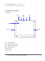
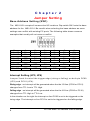
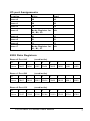
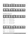
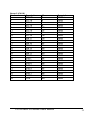
MSI -0101
PC/104 48 Bit Digital I/O Module
Quick Reference Manual
(Version 3.2)
Table of Contents
Chapter 0
Packing List
1
Chapter 1
Specifications
2
Chapter 2
Jumper Settings
4
Chapter 3
Operational Description
Chapter 4
Warranty
6
I/O Port Pin Assignment 10
12
iii
Chapter 0
Packing List
Function
MSI - 0101
Function
Package
48 Bit Digital I/O M S I - 0 1 0 1 4 8 B i t D i g i t a l I / O P C / 1 0 4
Module
Module
PC/104 Multi -I/O Module User's Manual
1
Chapter 1
Specifications
Description
The MSI -0101 is a 48-bit digital I/O module. The module can be used together with
TTL level input /output circuitry. Its 48 bits are arranged in two 24-bit digital I/O groups.
Each group emulates an 8255 PPI (programmable peripheral interface) mode 0, but
has a higher driving capacity than the 8255 PPI. Each 24-bit group is divided into
three 8-bit ports. A port can be configured to function as input or output.
l
48 digital I/O lines (2 groups)
l
Group emulates 8225 PPI mode 0
l
Buffered circuits for higher driving capacity than 8255 PPI
l
Bit 0 of port C can generate an interrupt to IRQ 2, 3, 4, 5, 6, 7
l
Interrupt trigger on rising / falling edge
l
Output status readback
l
Pin-compatible with OPTO-22 I/O module racks
l
Transfer rate: 300 KB/sec. (typical)
l
Digital output:
Logic level 0: 0.5 V max. @ 24 mA sink
Logic level 1: 2.0 V min. @ 15 mA source
l
Digital input:
Logic level 0: 0.8 V max.
Logic level 1: 2.0 V min.
Power requirements:
l
Single 5V @ 600 mA
Physical and Environmental
l
Dimensions: 95 x 90 mm
l
Weight: 100 gram
l
Operating temperature: 0 ~ +50°C
2
PC/104 Multi -I/O Module User's Manual
l
Storage temperature: -25 ~ +80°C
l
Relative humidity: 0 ~ 90% non-condensing
Component Location
MSI -0101
JP1
JP3
JP4
JP2
JP6
JP5
SW1
CN10
CN19
JP1 ~ JP2: IRQ select
JP3 ~ JP4: IRQ Level select
JP5 ~ JP6: IRQ Mode select
SW 1: Address select
CN10: Group 1
CN19: Group 2
PC/104 Multi -I/O Module User's Manual
3
Chapter 2
Jumper Setting
Base Address Setting (SW1)
The MSI -0101 occupies 8 consecutive I/O locations. Dip-switch SW1 sets the base
address for the MSI -0101. Be careful when selecting the base address as some
settings can conflict with existing PC ports. The following table shows common
examples that usually will not cause a conflict.
Hex
000-00F
010-01F
1
ON
ON
2
ON
ON
200-20F
210-21F
OFF
OFF
ON
ON
300-30F
OFF
OFF
3F0-3FF
OFF
OFF
3
ON
ON
………
ON
ON
……….
ON
……….
OFF
4
ON
ON
5
ON
ON
6
ON
OFF
ON
ON
ON
ON
ON
OFF
ON
ON
ON
OFF
OFF
OFF
Interrupt Setting (JP5, JP6)
J u m p e r 3 and 4 control the trigger edge (rising or falling) on both pin PC00
(JP3) and PC10 (JP4).
Rising edge : an interrupt will be generated when the the I/O line (PC00 or PC10)
changes from TTL Low to TTL High.
Falling edge : an interrupt will be generated when the the I/O line (PC00 or PC10)
changes from TTL High to TTL Low.
In the situation on the right the interrupt on line PC00 is set to be triggered on the
rising edge. The interrupt on line PC10 is set to be triggered on the falling edge.
4
PC/104 Multi -I/O Module User's Manual
Interrupt Mode (JP1, JP2)
The interrupt function can be enabled (INT) or disabled (DIS) by jumper setting. A
third option, a more dynamic approach, is to choose for an external device to
enable/disable the interrupt function (EXT).
Although you can only make one choice for both groups, the groups interrupt function
can be enabled/disabled separately when you choose for the EXT setting. Line PC04
and PC14 control the mode of interrupt for PC00 and PC10. TTL Low disables an
interrupt and TTL High enables an interrupt.
PC/104 Multi -I/O Module User's Manual
5
Chapter 3
Operational Description
Mode 0 Operation
Mode 0 operation provides simple input and output operation for each of the
three ports. No handshaking is required, data is simply written to or read from
a specific port.
Mode 0 Basic Functional Definitions:
- Three 8-bit ports
- Any port can be input or output
- Outputs are latched
- Inputs are not latched
6
PC/104 Multi -I/O Module User's Manual
I/O port Assignments
Location
W r ite
Re a d
Base+0
A0
A0
Base+1
B0
B0
Base+2
C0
C0
Base+3
Mode Register for N/A
A0, B0, C0
Base+4
A1
A1
Base+5
B1
B1
Base+6
C1
C1
Base+7
Mode Register for N/A
A1, B1, C1
8255 Data Registers
Base+0 Port A0
(read/write)
Bit
7
6
5
4
3
2
1
0
Value
PA07
PA06
PA05
PA04
PA03
PA02
PA01
PA00
Base+1 Port B0
(read/write)
Bit
7
6
5
4
3
2
1
0
Value
PB07
PB06
PB05
PB04
PB03
PB02
PB01
PB00
Base+2 Port C0
(read/write)
Bit
7
6
5
4
3
2
1
0
Value
PC07
PC06
PC05
PC04
PC03
PC02
PC01
PC00
PC/104 Multi -I/O Module User's Manual
7
Base+4 Port A1
(read/write)
Bit
7
6
5
4
3
2
1
0
Value
PA17
PA16
PA15
PA14
PA13
PA12
PA11
PA01
Base+5 Port B1
(read/write)
Bit
7
6
5
4
3
2
1
0
Value
PB17
PB16
PB15
PB14
PB13
PB12
PB11
PB10
8255 Mode Registers
Base+4 Port A0, B0, C0
(write)
Bit
7
6
5
4
3
2
1
0
Value
1
0
0
PA0
PC0
0
PB0
PC0
PA0=0
à
Port A0 is oupput
PA0=1
à
Port A0 is input
PB0=0
à
Port B0 is oupput
PB0=1
à
Port B0 is input
PC0=0
à
Port C0 is o u p p u t
PC0=1
à
Port C0 is input
Base+7 Port A1, B1, C1
(write)
Bit
7
6
5
4
3
2
1
0
Value
1
0
0
PA0
PC0
0
PB0
PC0
PA0=0
à
Port A0 is oupput
PA0=1
à
Port A0 is input
PB0=0
à
Port B0 is oupput
PB0=1
à
Port B0 is input
8
PC/104 Multi -I/O Module User's Manual
PC0=0
à
Port C0 is oupput
PC0=1
à
Port C0 is input
Note:
After power-on or reset of the module the A0, B0, C0, A1, B1 and C1 ports are default
set to input mode!
PC/104 Multi -I/O Module User's Manual
9
Chapter 4
I/O Port Pin Assignment
Group 1 (CN 10)
Pin
Description
Pin
Description
1
3
5
7
9
11
13
15
17
19
21
23
25
27
29
31
33
35
37
39
41
43
45
47
49
2
4
6
8
10
12
14
16
18
20
22
24
26
28
30
32
34
36
38
40
42
44
46
48
50
GND
GND
GND
GND
GND
GND
GND
GND
GND
GND
GND
GND
GND
GND
GND
GND
GND
GND
GND
GND
GND
GND
GND
GND
GND
10
PC07
PC06
PC05
PC04
PC03
PC02
PC01
PC00
PB07
PB06
PB05
PB04
PB03
PB02
PB01
PB00
PA07
PA06
PA05
PA04
PA03
PA02
PA01
PA00
+5V
PC/104 Multi -I/O Module User's Manual
Group 2 (CN 19)
Pin
Description
Pin
Description
1
3
5
7
9
11
13
15
17
19
21
23
25
27
29
31
33
35
37
39
41
43
45
47
49
2
4
6
8
10
12
14
16
18
20
22
24
26
28
30
32
34
36
38
40
42
44
46
48
50
GND
GND
GND
GND
GND
GND
GND
GND
GND
GND
GND
GND
GND
GND
GND
GND
GND
GND
GND
GND
GND
GND
GND
GND
GND
PC17
PC16
PC15
PC14
PC13
PC12
PC11
PC10
PB17
PB16
PB15
PB14
PB13
PB12
PB11
PB10
PA17
PA16
PA15
PA14
PA13
PA12
PA11
PA10
+5V
PC/104 Multi -I/O Module User's Manual
11
Warranty
This product is warranted to be in good working order for a period of one
year from the date of purchase. Should this product fail to be in good
working orderat any time during this period, we will, at our option, replace or
repair it at noadditional charge except as set forth in the following terms.
This warranty doesnot a pply to products damaged by misuse, modifications,
accident or disaster. Vendor assumes no liability for any damages, lost
profits, lost savings or anyother incidental or consequential damage
resulting from the use, misuse of, orinability to use this product. Vendor will
not be liable for any claim made by anyother related party. Return
authorization must be obtained from the vendor before returned merchandise will be accepted. Authorization can be obtained by calling or faxing the
v e n d o r a n d r e q u e s t i n g a Return Merchandise Authorization (RMA) number.
Returned goods should always be accompanied by a clear problem
description.
12
PC/104 Multi -I/O Module User's Manual