1
ABSTRACT
GODBOLE, RAHUL PUSHPAK. Design of a Flexible DSP Based Controller Hardware
System for Power Electronics Applications. (Under the direction of Prof. Subhashish
Bhattacharya).
This thesis proposes the concept of a universal controller hardware system for
power electronics applications. With the presence of generic interfaces and communication
schemes, this system can be used in various other control scenarios. A prototype hardware
system incorporating a high performance floating point digital signal processor (DSP) and a
powerful field programmable gate array (FPGA) has been built to demonstrate the concept
of real-time hardware simulation. Prior to being deployed for control of a complete power
electronics system, an intermediate step that would yield more information pertaining to
system timing is the hardware simulation enabled by such a board. Extracting maximum
throughput from this system with a few innovative schemes has been another goal of this
project. In order to achieve this objective, the embedded peripherals of the Texas Instruments C6000 series DSP have been programmed to facilitate a higher degree of parallelism.
The core of this thesis deals with the different sub-systems that comprise the real-time
controller (RTC) board, and their interaction with one another. One of the novel schemes
proposed in this thesis involves the on-board communication between the DSP and several
analog-to-digital converter (ADC) chips using the multi-channel audio serial port (McASP)
peripheral. The efficacy of this concept is made possible by a robust software architecture,
enabled by the enhanced direct memory access (EDMA) peripheral. In addition to the
DSP peripheral activity, significant processing capability is offered by the Cyclone II series
FPGA. The option of universal connectivity is provided over either ethernet or USB. The
FPGA also provides a platform for developing a complete system with an embedded 32-bit
processor. The RTC board prototype can be used for power electronics applications with
the addition of certain interface boards, which can be readily developed.
Design of a Flexible DSP Based Controller Hardware System for Power Electronics
Applications
by
Rahul Pushpak Godbole
A thesis submitted to the Graduate Faculty of
North Carolina State University
in partial fullfillment of the
requirements for the Degree of
Master of Science
Electrical Engineering
Raleigh, North Carolina
2008
APPROVED BY:
Dr. Alexander G. Dean
Dr. Alex Q. Huang
Dr. Subhashish Bhattacharya
Chair of Advisory Committee
DEDICATION
To
Mama - Papa
ii
BIOGRAPHY
Rahul Pushpak Godbole was born on 6th November 1981 in Pune, India. He received the
Bachelor of Engineering (B.E.) Degree in Electronics and Telecommunication Engineering
from Government College of Engineering Pune (C.O.E.P.), University of Pune in 2003. He
worked briefly as a Programmer Analyst at Cognizant Technology Solutions Pune, India.
Thereafter he worked for about 2 years as an Electronic Design Engineer at Honeywell
Automation India Limited, Pune, India.
Rahul has been a graduate student in the Electrical and Computer Engineering Department at North Carolina State University, Raleigh, NC since Spring 2006. He completed a
three month summmer internship in the summer of 2007 with Qualcomm Incorporated in
the processor verification group at Cary, NC. He is a member of the Honor Society of Phi
Kappa Phi.
iii
ACKNOWLEDGMENTS
Through my two year stay at the SPEC lab and the ECE department in NCSU, I have had
the fortune of working with some of the most brilliant minds in the electrical engineering
field.
I would like to thank Dr. Alex Dean who helped me develop a good understanding
in the field of embedded systems. It was in my first semester at NC State, when I took
his embedded system design course, that I understood the broad areas of application of
embedded systems. Our SPEC center director, Dr. Alex Huang, has always been a source
of inspiration. His insightful inputs during our weekly SPEC team meetings gave a certain
sense of direction for my work. A special thank you is also due to my primary advisor Dr.
Subhashish Bhattacharya, who was always there to guide my work. He has proved to be
much more than a research advisor for me, and I am very grateful that I got a chance to
work with him on this project.
The friendships and working relationships I built over the course of my stay at the
SPEC lab will be cherished by me forever. Honest feedback and collaborative work with
Sameer, Peter and Zhigang helped me a great deal when I needed it the most.
I have never had a chance to thank my family for being my pillar of strength and
support. My parents were very encouraging of my work from the outset. Anupama, Smita,
Raj and Ash were my extended family away from home. The person I would like to thank
the most however, is my wife Namrata, for being so very patient and understanding through
the course of my Masters studies.
All work with no fun would have really made education incomplete at NC State. I
found a bunch of excellent roommates in Abhishek, Binoy, Nikhil, Amod, Rajeev, Sampath,
Mohan, Ghatol, Kanishka, Abhay and Gautam. That was a whole lot of housemates to
have over the course of two years. Our weekend gang of Pande, Mehra, Vas, Kundi and
Bob always helped ease any work pressure that may have existed. Life at NC State was
complete thanks to all these guys.
iv
v
TABLE OF CONTENTS
LIST OF FIGURES . . . . . . . . . . . . . . . . . . . . . . . . . . . . . . . . . . . . . . . . . . . . . . . . . . . . . . vii
LIST OF TABLES . . . . . . . . . . . . . . . . . . . . . . . . . . . . . . . . . . . . . . . . . . . . . . . . . . . . . . . . ix
1 Introduction . . . . . . . . . . . . . . . . . . . . . . . . . . . . . . . . . . . . . . . . . . . . . . . . . . . . . . . . . . .
1.1 Overview . . . . . . . . . . . . . . . . . . . . . . . . . . . . . . . . . . . . .
1.2 Previous Work . . . . . . . . . . . . . . . . . . . . . . . . . . . . . . . . . .
1.3 Organization . . . . . . . . . . . . . . . . . . . . . . . . . . . . . . . . . . .
1
1
2
3
2 Specification and Device Selection . . . . . . . . . . . . . . . . . . . . . . . . . . . . . . . . . . . . .
2.1 System Hardware Requirements . . . . . . . . . . . . . . . . . . . . . . . . .
2.2 Device Selection . . . . . . . . . . . . . . . . . . . . . . . . . . . . . . . . .
2.2.1 Differential to Single ended converter . . . . . . . . . . . . . . . . . .
2.2.2 Analog to Digital Converter . . . . . . . . . . . . . . . . . . . . . . .
2.2.3 Digital Signal Processor . . . . . . . . . . . . . . . . . . . . . . . . .
2.2.4 Field Programmable Gate Array . . . . . . . . . . . . . . . . . . . .
5
5
7
7
8
11
15
3 System Architecture . . . . . . . . . . . . . . . . . . . . . . . . . . . . . . . . . . . . . . . . . . . . . . . . . . .
3.1 Overview of the System Hardware . . . . . . . . . . . . . . . . . . . . . . .
3.2 Hardware Design . . . . . . . . . . . . . . . . . . . . . . . . . . . . . . . . .
3.2.1 Power Supply Design . . . . . . . . . . . . . . . . . . . . . . . . . . .
3.2.2 Differential to Single Ended Converter . . . . . . . . . . . . . . . . .
3.2.3 ADC-DSP Interface . . . . . . . . . . . . . . . . . . . . . . . . . . .
3.2.4 External Memory Interfacing . . . . . . . . . . . . . . . . . . . . . .
3.2.5 FPGA and peripherals . . . . . . . . . . . . . . . . . . . . . . . . . .
19
19
21
22
25
27
31
34
4 Hardware Software Co-design . . . . . . . . . . . . . . . . . . . . . . . . . . . . . . . . . . . . . . . . . .
4.1 DSP Software Setup . . . . . . . . . . . . . . . . . . . . . . . . . . . . . . .
4.1.1 GEL File Programming . . . . . . . . . . . . . . . . . . . . . . . . .
4.1.2 Linker Command File Setup . . . . . . . . . . . . . . . . . . . . . .
4.2 ADC Interface using DSP Peripheral Programming . . . . . . . . . . . . . .
4.2.1 ADC Timing Specifications . . . . . . . . . . . . . . . . . . . . . . .
4.2.2 McASP Configuration Setup . . . . . . . . . . . . . . . . . . . . . .
4.2.3 EDMA Setup . . . . . . . . . . . . . . . . . . . . . . . . . . . . . . .
4.3 FPGA - Digital Logic and Embedded Processor Programming . . . . . . . .
4.3.1 Logic Implementation . . . . . . . . . . . . . . . . . . . . . . . . . .
4.3.2 SOPC Builder System . . . . . . . . . . . . . . . . . . . . . . . . . .
38
38
39
42
43
43
45
49
55
56
57
vi
5 Results and Conclusion . . . . . . . . . . . . . . . . . . . . . . . . . . . . . . . . . . . . . . . . . . . . . . . . 59
5.1 Hardware Results . . . . . . . . . . . . . . . . . . . . . . . . . . . . . . . . .
59
5.2 Conclusion and Recommendations for Future Work . . . . . . . . . . . . . .
61
Bibliography . . . . . . . . . . . . . . . . . . . . . . . . . . . . . . . . . . . . . . . . . . . . . . . . . . . . . . . . . . . . . 63
Appendices . . . . . . . . . . . . . . . . . . . . . . . . . . . . . . . . . . . . . . . . . . . . . . . . . . . . . . . . . . . . . . . 66
A Firmware Code for DSP . . . . . . . . . . . . . . . . . . . . . . . . . . . . . . . . . . . . . . . . . . . . . . . 67
A.1 Main() function . . . . . . . . . . . . . . . . . . . . . . . . . . . . . . . . . .
67
A.2 McASP configuration . . . . . . . . . . . . . . . . . . . . . . . . . . . . . . .
69
A.3 EDMA Configuration . . . . . . . . . . . . . . . . . . . . . . . . . . . . . .
73
vii
LIST OF FIGURES
Figure 2.1 Comparison of SAR and Sigma Delta Converters . . . . . . . . . . . . . . . . . . . . . . . . . . .
9
Figure 2.2 C6713B DSP Functional Block Diagram [1] . . . . . . . . . . . . . . . . . . . . . . . . . . . . . . . . 15
Figure 3.1 System Block Diagram of Real Time Controller and Interfacing boards . . . . . 20
Figure 3.2 Block Diagram of Real Time Controller Board . . . . . . . . . . . . . . . . . . . . . . . . . . . . . 21
Figure 3.3 Typical schematic of TPS5461x regulator [2] . . . . . . . . . . . . . . . . . . . . . . . . . . . . . . . 23
Figure 3.4 Switching frequency trimming resistor selection [2] . . . . . . . . . . . . . . . . . . . . . . . . . 23
Figure 3.5 Simulation Circuit used for INA2132 biasing selection . . . . . . . . . . . . . . . . . . . . . . 26
Figure 3.6 Transient characteristics showing differential to single ended conversion . . . . 26
Figure 3.7 Hardware connections for ADS8345-C6713 DSK interface . . . . . . . . . . . . . . . . . . 27
Figure 3.8 Hardware connections for MAX1168-C6713 DSP for RTC board . . . . . . . . . . . 30
Figure 3.9 McASP Block Diagram . . . . . . . . . . . . . . . . . . . . . . . . . . . . . . . . . . . . . . . . . . . . . . . . . . . . 32
Figure 3.10 128MB Micron SDRAM Connection on EMIF Bus . . . . . . . . . . . . . . . . . . . . . . . . 33
Figure 3.11 Memory Map of DSP for Real Time Controller Board . . . . . . . . . . . . . . . . . . . . . 34
Figure 3.12 Cyclone II FPGA Internal Architecture [3] . . . . . . . . . . . . . . . . . . . . . . . . . . . . . . . . 35
Figure 3.13 Configuration scheme for RTC board FPGA - Active Serial and JTAG . . . . 37
Figure 4.1 Serial digital interface timing diagram for MAX1168 [4] . . . . . . . . . . . . . . . . . . . . 44
Figure 4.2 Individual serializer and connections within McASP [5]. . . . . . . . . . . . . . . . . . . . . 46
Figure 4.3 Transfer format for RTC board . . . . . . . . . . . . . . . . . . . . . . . . . . . . . . . . . . . . . . . . . . . . 51
Figure 4.4 EDMA Transfer from Memory to McASP XMT . . . . . . . . . . . . . . . . . . . . . . . . . . . . 51
Figure 4.5 EDMA Transfer from McASP RCV to Memory . . . . . . . . . . . . . . . . . . . . . . . . . . . . 52
Figure 4.6 Ping-pong operation for both XMT and RCV McASP sections . . . . . . . . . . . . . 54
viii
Figure 4.7 FPGA Hierarchical View of Internal Modules . . . . . . . . . . . . . . . . . . . . . . . . . . . . . . 56
Figure 4.8 Example SOPC Builder System with USB PHY ISP1362 . . . . . . . . . . . . . . . . . . . 57
Figure 5.1 Real-Time Controller Board Prototype . . . . . . . . . . . . . . . . . . . . . . . . . . . . . . . . . . . . . 60
Figure 5.2 DSP Code Composer Studio Memory Snapshot for Ping-pong buffering . . . . 61
Figure 5.3 Real-time Hardware Simulation Results . . . . . . . . . . . . . . . . . . . . . . . . . . . . . . . . . . . . 62
ix
LIST OF TABLES
Table 2.1 Difference Amplifier Comparison Chart . . . . . . . . . . . . . . . . . . . . . . . . . . . . . . . . . . . . .
8
Table 2.2 A-to-D Converter Comparison Chart. . . . . . . . . . . . . . . . . . . . . . . . . . . . . . . . . . . . . . . . 11
Table 4.1 Configuration register in RTC board for MAX1168 . . . . . . . . . . . . . . . . . . . . . . . . . . 45
Chapter 1
Introduction
1.1
Overview
Real-time control and complete system simulation in hardware are fairly typical in power
electronics. The concepts of data acquisition and high-speed digital input/output are a
requirement for these applications. The IO requirement for power electronic systems tends
to be very high. This is due to the large number of variables to be controlled in the system,
which on several occassions includes not just the power electronic devices, but also the
connected electric load. Consequently, the processing requirement on the control system
also tends to grow exponentially.
Controllers for power electronics tend to be very application specific. Off the shelf
controllers do not exist for power electronics applications. This is more of a problem as
we move towards large converter controls. A couple of proprietary control systems, such as
the Simatic TDC from Siemens and the Mach II from ABB, designed for power electronic
converters have successfully accomplished real-time control. These are large multi-processor
systems with extreme computational capability. However, besides being very expensive,
these systems need to be used in conjunction with the power converter systems provided
by these very manufacturers. This is a constraint very few would be able to work with.
This thesis aims to develop a generic control system that could be applied for
different applications in power control. A power electronics converter based system is taken
1
2
as the base for demonstrating the effectiveness of the proposed architecture. Prior to the
real-time control of these systems, hardware in the loop simulation of the controlled variables is an added feature of the controller. The flexible interface nature of the proposed
architecture make it ideal for hardware simulation of any data acquisition type system.
1.2
Previous Work
A few control systems developed in academic labs have proposed architectures that
have been employed for the control of power electronic systems. These form the subject of
discussion in this section.
WEMPEC Reconfigurable Real-Time Controller
This system has been developed at the University of Wisconsin, Madison [6]. The
closed loop digital control of power electronic systems is obtained with a 32-bit floating
point 50MHz TMS320C31 DSP from Texas Instruments. The Xilinx XCS40 FPGA is used
to implement PWM functionality required for providing the switching signals for power
electronic converters. The processing capability of this controller is inadequate as per the
requirements that will be outlined in chapter 2. Moreover, this controller uses 12-bit serial
A-to-D converters. Ideally, a higher ADC resolution is a requirement for real-time digital
control in power electronics.
Versatile DSP/FPGA structure from University of Aachen
The versatile DSP/FPGA structure proposed by Claus Ulrich [7] has a number
of attractive features. It introduces the concept of a flexible hardware structure that can
be used for implementing real-time digital control and hardware in the loop simulation
of control systems. The computing core of this system is the SHARC DSP from Analog
Devices, which is a 40MHz floating point CPU. The FPGA used on-board is a Lucent
Technology FPGA that can be used for booting along with the SHARC DSP. Similar to the
WEMPEC board, this system also has limited throughput rate, which can be a hindrance
when it comes to developing robust control systems.
3
Digital Controller for STATCOM Systems at NC State University
The digital controller for Cascaded Multi-level Converter (CMC) based static synchronous compensators (STATCOM) systems proposed by Yang [8] is used as a reference
point for developing the controller board in this lab. The DSP used in this system is the
C6713B DSP, which is identical to the one that will be used in this thesis. However, the
DSP in this system is present on an evaluation board provided by TI. Due to the limited
nature of IO from this evaluation board, a daughter card incorporating a separate FPGA,
interfaced with front-end 12-bit ADCs, is connected to the DSK board. The architecture of
this system has 3 different FPGA devices (on separate boards) to accomplish PWM functionality and high-speed digital IO. This makes the system unnecessarily large and unwieldy.
The ADC resolution also could use improvement here.
One common thing in all the above systems is the method of interfacing ADC
channels with the DSP. An indirect scheme is used in all these architectures, implying that
the FPGA acts as the intermediate link between serial ADCs and the DSP. This is done to
offload the CPU activity from ADC processing. System throughput can be increased with
another scheme, as will be outlined in chapter 4.
This section has touched upon a few controller architectures proposed for accomplishing power electronic control. With the growing hardware and software requirement on
control systems, these controllers become unsuitable for system expansion. Chapter 2 deals
with the necessary specifications for the example system. The controller architecture being
proposed as a part of this thesis aims to overcome some of the limitations of the existing
systems, while providing additional throughput and a few extra features.
1.3
Organization
The rest of the thesis is organized as follows. Chapter 2 outlines the actual system
specifications in terms of hardware and software requirements. These system requirements
naturally lead into the components that would enable us to meet these specifications. Hence,
the selection of specific devices or components that go into the control hardware is covered
in detail in this chapter. Chapter 3 describes the architecture of the real-time controller.
This chapter also serves as a detailed hardware design document for the control board. The
various sub-system connections are described here from a hardware perspective. Some of the
4
device specific hardware considerations are also described in this chapter. Chapter 4 deals
with the underlying firmware for the DSP as well as the HDL and embedded firmware and
HDL of the FPGA. This chapter describes the software details of the ADC-DSP interface in
order to be in agreement with the ADC timing requirement. As this chapter deals with some
of the partitioning of tasks in both hardware and software, it is befitting that this chapter
be titled hardware software co-design. Chapter 5 shows a few hardware simulation results.
It also provides a conclusion with recommendations for future work. The appendices at the
end of the thesis include source code for the DSP used on the RTC board.
Chapter 2
Specification and Device Selection
Although the goal of this project is to develop a generic system that could be applied
for control of power electronic systems, its interaction with the external world needs to be
well defined. This chapter details the specification requirement of an example system that
will be used to demonstrate the working of the controller board. The next few sections
can serve as a reference point for systems that will be interfacing with this board. The
system specification leads into the device selection parameters. These criteria will also
be touched upon, with a comparative study of different devices that were considered for
implementation. Components of interest in the signal chain that are analyzed in this chapter
include the analog signal buffer op-amp, the analog to digital converter (ADC), the digital
signal processor (DSP) and the field programmable gate array (FPGA).
2.1
System Hardware Requirements
A study of different existing systems for accomplishing power control was done
to formulate a set of requirements for the real-time controller (RTC) board. A few key
specifications are listed here in decreasing order of importance, with a brief explanation
provided for each.
• Floating point signal processing is a must for this system. The problem of scaling
inherent with fixed point processing is to be avoided at any cost. The loss of precision
5
6
with fixed point implementation can have a significant impact in a high power system.
• System processing rate:
– The processing capability of the DSP needs to be significantly large - in the
order of about 800 million instructions per second [8]. This figure does take the
input/output requirement of the system into account.
– The ADC througput rate needs to be such that analog signals are sampled within
1 degree of resolution of the fundamental frequency of 60Hz. This leads to a
time between successive analog channel conversions of 46µsec. This figure also
indicates the total program time, implying that the entire control loop needs to
be executed within the cycle time of 46µsec.
• Differential analog input provision. The interface provided with the signal conditioning board needs to have an option of being differential in nature to increase the
noise immunity of the system. At the same time, single ended signals should also be
accomodated.
• Number of analog inputs: 32. This is a worst case estimate of the number of analog
inputs that would be connected to a single controller system. These analog signals
include the three-phase voltage levels, the reference currents and any other analog
control signals for a power electronic converter system.
• The above specification also leads to the requirement of serial A-to-D converters.
Parallel converters for 32 analog channels would significantly increase the real estate
on the board. Moreover, serial ADCs used in conjunction with DSPs have the ability
to exceed the processing speed expectation from the system.
• The ADC resolution desirable is 16 bits, specially with the power electronics systems in
place as of today. Earlier systems were limited to a maximum of 14 bits of resolution,
but the effective number of bits (ENOB) was obviously lower than that. Consequently,
with the signal levels being dealt with, 16 bit resolution, with an acceptable ENOB
of 14 bits is an important requirement.
• Number of digital input/outputs (including digital PWM): approx 128. This again is
an estimate of the number of status signals, PWM outputs, relay operating signals
among other digital IO that will be in use for the system.
7
• Voltage signal levels internal to the system i.e. on board will be at the nominal 3.3V
digital signal level prevalent these days. As the interface with external boards is at
the 5V level, buffers will need to be provided. Moreover, the analog inputs will need
to be constrained to a peak to peak amplitude of +/-2.5V when interfaced with the
system.
• Universal connectivity provided over USB or Ethernet. This has been a very desirable feature of all generic control systems for long. Numerous systems incorporating
various industrial interface standards including Ethernet, Profibus or even CAN bus
protocols exist. These systems tend to win over those that have limited connectivity.
An important feature that gets added to the system with this level of connectivity is
the merging of control and communication hardware on the same board. In a communication scenario, each board acts as a node, to communicate with other nodes on
the network. The emerging area of power electronics control over a network interface
can thus get a system for validation of the ”control and communication” concepts.
2.2
Device Selection
This section discusses the details of the selection criteria used for different de-
vices on-board. Where possible, the vendor specific selection is presented as well with a
comparative study of the options available.
2.2.1
Differential to Single ended converter
The entire signal chain for the system starts with an analog signal processing
board that is separate from the board being designed. The signal conditioning circuitry
that includes stages of operational amplifiers and analog filters is outside the scope of this
document. The first stage of devices in the signal chain encountered on the RTC board is
the differential to single ended analog signal converter. A unity gain difference amplifier
needs to be used for this purpose.
As stated in [9], the first and foremost parameters to be seen in the selection of an
op-amp are the Gain Bandwidth product (GBW) and the slew rate. To pre-empt component
induced errors, amplifiers with a fixed gain G=1 are chosen. Also, the bandwidth needs
8
to be atleast 100 times the maximum signal frequency content. Difference amplifiers from
several manufacturers were considered, before narrowing down on the following four options
- AD629 and AMP03 from Analog Devices(ADI), and INA132 and INA2132 from Texas
Instruments(TI).
Table 2.1: Difference Amplifier Comparison Chart
Amplifier
AD629 [10]
AMP03 [11]
INA132 [12]
INA2132 [13]
Bandwidth
500kHz
3MHz
300kHz
300kHz
Slew Rate
2.1V/µs
9.5V/µs
0.1V/µs
0.1V/µs
Channels
Single
Single
Single
Dual
CMRR
77dB
100dB
90dB
90dB
Package
8SOIC
8SOIC
8SOIC
14SOIC
As per the comparison table 2.1, the amplifiers from ADI have excellent GBW
and slew rate. The two amplifiers from TI also have very good performance, keeping the
application in mind. As the frequencies of interest for conversion (including upto the tenth
harmonic) will not exceed 1kHz, both the slew rate and GBW product of the TI amplifiers
are well over the acceptable limit. Moreover, since real estate of the board is another
important criterion, the dual op-amp INA2132 is selected for the RTC board. This
op-amp also has the capability to sustain higher input voltages, thus providing automatic
protection of the input circuitry in the system.
2.2.2
Analog to Digital Converter
Following the op-amp is the single ended analog input ADC. It is desirable for
this device to satisfy a few other important characteristics besides the ones listed in the
specification section. These parameters and the final device selection will be outlined in
this section. This happens to be one of the most important devices in the system as it
bridges the world of analog and digital. Errors occurring in this device could potentially be
devastating for the application. Hence, it is crucial that the selected ADC meet the system
specifications.
The application being targeted dictates that a 16-bit resolution serial A-to-D converter be used. The different ADC architecture options that can be explored include the
Successive Approximation Register (SAR) type, Sigma Delta, Flash converter, Voltage-toFrequency and Pipeline converters. Out of these, only the first two can be applied suitably
9
for the application. Typically, SAR ADCs are used for data acquisition systems, and sigma
delta ADCs find use in industrial measurement and multimedia applications. Figure 2.1
shows a qualitative comparison of the SAR ADC with the Sigma Delta converters. As
the graph indicates, the accuracy of sigma delta ADCs is better than SAR ADCs at low
throughput. However, this accuracy begins to drop off as the sampling frequency (which
depends on the throughput rate) increases. Depending on the number of channels we are
able to integrate in one ADC, a lower throughput may be acceptable for the RTC board.
Hence, both sigma delta and SAR ADCs have been considered.
Figure 2.1: Comparison of SAR and Sigma Delta Converters
Accuracy of the ADC is dependent on several key specs, which include integral
nonlinearity error (INL), offset and gain errors, and the accuracy of the voltage reference,
temperature effects, and AC performance. It is best to begin the ADC analysis by reviewing
the DC performance, because ADCs use a plethora of nonstandardized test conditions for
the AC performance, making it easier to compare two ICs based on DC specifications. The
DC performance will in general be better than the AC performance[14].
Though not mentioned as a key parameter for an ADC, the differential nonlinearity
(DNL) error is the first specification to observe. DNL reveals how far a code is from a
neighboring code. The distance is measured as a change in input-voltage magnitude and
10
then converted to LSBs. Note that INL is the integral of the DNL errors, which is why
DNL is not included in the list of key parameters. The key for good performance for an
ADC is the claim ”no missing codes.” This means that, as the input voltage is swept over
its range, all output code combinations will appear at the converter output. A DNL error
of less than ± 1LSB guarantees no missing codes. With a value equal to -1LSB, the device
is not necessarily guaranteed to have no missing codes. Whereas, a DNL value greater than
± 1LSB implies that the device has missing codes. The DNL specification implies that the
accuracy of the ADC is more often than not less than the stated resolution in terms of
number of bits. A more standard comparison of ADCs is done keeping this in mind.
The AC performance of the ADC includes signal to noise ratio SNR specified in
terms of signal to noise and distortion (SINAD) and total harmonic distortion (THD). For
the device selection, DC parameters will be used for comparison, while ensuring that the
AC specifications of the selected device are within acceptable limits. AC specifications of
an ADC imply repeatability, whereas DC specifications guarantee accuracy of a converter.
The only AC parameter that will be used in the comparative analysis is the effective number
of bits (ENOB) of ADCs. This is defined as follows:
EN OB =
SIN AD − 1.76
6.02
(2.1)
Note: In equation 2.1, SINAD is expressed in dB.
As external analog multiplexing will not be adopted in the RTC board, the shortlisted ADCs for comparison would need to have a minimum of 4 analog inputs. Typically,
internal multiplexing of analog channels is employed in these devices. This requirement
places a few restrictions on the form factors of the ADCs that will be considered. Serial
ADCs have a smaller form factor and will be considered for comparison over parallel ADCs
for this board.
The ADCs that have been used for comparison include one sigma delta converter
viz. ADS1178 from Texas Instruments. All other ADCs that come close to meeting the
requirements are SAR type converters. From the comparison table 2.2, it is clear that
the ADCs from the three manufacturers Analog Devices (AD7656), Texas Instruments
(ADS1178, ADS8342 and ADS8345) and Maxim Semiconductor (MAX1168) match closely
in their performance characteristics. Going back to the specification 2.1, the ADC should
11
Table 2.2: A-to-D Converter Comparison Chart
ADC
AD7656
ADS1178
ADS8342
ADS8345
MAX1168
Num Channels
6
8
8
8
8
ENOB
13.9
15.7
14
15
14.2
DNL
2LSB
1LSB
1LSB
1LSB
1LSB
Throughput
250kSps
52kSps
250kSps
100kSps
200kSps
Package
64LQFP
64HTQFP
48TQFP
20SSOP
24SOIC
be able to match the system throughput to give atleast 46µs between conversions. As 8
channels will be cycled through, the actual cycle time for one ADC needs to be atleast 46/8
i.e. approx 8µs. This leads to a sampling frequency of atleast 125kHz. There is a tradeoff
involved in the selection of the ADC here. From the candidate ADCs that have a sampling
rate greater than 125kHz, both AD7656 and ADS8342 have a fairly large form factor. The
16-bit 8-channel 200kSPS MAX1168 ADC satisfies all the selection criteria while
providing readings within the acceptable error limit.
Moreover, the MAX1168 has several attractive features on the serial digital interface side, which none of the other ADCs that were considered had. These features will be
outlined in chapter 3.
2.2.3
Digital Signal Processor
Further down the signal chain, the digital equivalent of the analog input is passed
to the DSP from the ADC. The DSP selection criteria have been stated in this section, with
a justification of the selected DSP.
First of all, when the system specifications were stated, DSP was not the only
architecture that was considered for the application. There are numerous architecture
options available for implementing the digital control functionality in most control systems
besides DSP, viz. custom ASIC solution, FPGA and even a general purpose processor
implementation. However, where the DSP architecture scores over the others for the RTC
board application are the following:
1. Dedicated multiply accumulator (MAC) unit in hardware - the control loop that
needs to be implemented uses heavy computation that needs to be completed in a
finite interval of time (requirements stated in the specification section). The Parks
12
Transform equation which is repeatedly executed to convert from ABC to DQ0 coordinates in power electronics, needs a multiply accumulate operation for efficient
execution. Most general purpose processors do not have the MAC unit and as a
result consume precious multiple cycles for executing the MAC operation. Although
ASIC implementations would yield the best performance for a given application, the
development cycle time is rarely justified. Certain FPGAs do contain MAC units, but
this requires additional device resources to be consumed for implementation. Hence,
a DSP is preferred for this very efficient piece of hardware.
2. The computation performance of the DSPs that will be considered can be in the order
of what is required for the RTC board application. The 800 MIPS requirement stated
earlier can be easily achieved with good DSP architectures.
3. A side advantage of using DSPs is the peripherals it offers for use. Due to the signal
processing capability, multimedia application requirements have tended to influence
the DSP peripheral provision. These very peripherals can be leveraged for power
electronics control functions. The subsequent chapters will show how one of these
peripherals viz. Multichannel Audio Serial port (McASP), designed primarily for
audio applications has been applied for multiple ADC interfacing, thus providing an
elegant solution for our control application.
As the decision to select a DSP as the processor for the RTC board is evident, the
next step is evaluation of different DSP architectures. While DSPs from Analog Devices
were considered, the comparative analysis done below talks more about those from Texas
Instruments. This was primarily due to existing systems incorporating TI DSPs. Moreover,
the initial study of these DSPs showed that TI DSP architectures had covered the gamut
of applications being addressed by Analog Devices DSPs as well.
TI C2000 High Performance 32-bit Controllers
The first controllers that were considered for the task at hand were the C2000
controllers that are optimized for motor control applications. Some of the advantages of
this series of DSP are the following:
1. Presence of on-chip PWM functionality.
13
2. On-chip A-to-D converter.
3. Latest series of TMS320F283xx DSPs having floating point performance.
4. Two multi-channel buffered serial ports (McBSP) for interfacing serial peripherals.
Even though these devices have a few of the attractive features listed above, the
limitations of their peripherals (as far as meeting the specifications is concerned) were as
follows:
1. The highest end DSP in this series has only 18 CH of PWM available. There are an
additional 88 general purpose IO (GPIO) available on the F28xx series controllers.
The application requirements stated earlier necessitate the presence of atleast 120
GPIO. As stated in the next section, only a FPGA would be capable of meeting this
requirement. Hence, the presence of this peripheral does not offer too much of an
advantage for our application.
2. There is one 16-CH 12-bit ADC on the highest end DSP. Our application needs a
16-bit resolution ADC with 32 input channels. Hence, this ADC peripheral on the
C2000 series DSP cannot be adequately exploited.
3. The serial port peripheral Multichannel buffered serial port (McBSP) is adequate for
interfacing only one serial input. As this DSP has 2 ports, a maximum of 2 serial
channels can be interfaced. For higher number of channels to be interfaced, it would
be necessary to employ external multiplexing, which we have avoided for the RTC
board. For direct interfacing with upto 32 channels, a more powerful peripheral such
as the multi-channel audio serial port (McASP) is preferred.
C6000 Floating Point DSP
The C6000 series of TI DSPs has two versions viz. the performance value DSP,
which is essentially a fixed point DSP and the other one being the Floating point series
DSP. Although these devices are ideal for multimedia, imaging and voice applications, the
features offered by them can be successfully exploited for industrial control applications as
well.
A few of the key features that worked in favor of the C6000 floating point DSP
were as follows:
14
1. Certain DSPs in this series have frequencies of operation in excess of 200MHz. This
makes the DSP ideal for achieving a throughput well in excess 1000 MIPS, leaving a
lot of margin for future expansion of the system such as upgrading from the existing
3-level Static synchronous compensator (STATCOM) to a 13-level STATCOM [8].
2. Rich set of peripherals, such as the External Memory Interface (EMIF), Enhanced
Direct Memory Access (EDMA) and serial peripherals.
3. The Multichannel Audio serial port (McASP) peripheral makes it easier to work with
multiple serial ADCs. The detailed description of this peripheral interfaced with the
MAX1168 ADC is included in the next chapter.
The C6713B DSP was shortlisted from the portfolio of C6000 DSPs. As all devices
in the C6000 series have an identical set of peripherals, the deciding factor proved to be
the core voltage for powering the DSP. It should be noted that the selection of the DSP
was done in conjunction with the FPGA selection. Having a common core voltage for the
two devices was deemed necessary for reducing the number of power supplies required on
board. The C6713B DSP has a core supply of 1.2V, which is identical to that required by
the Cyclone II series FPGA (selection outlined in next section). The IO supply operates
off the standard 3.3V digital interface.
Figure 2.2 depicts the full architectural characteristics of the C6713B DSP. The
peripherals that are of interest for the RTC board have been highlighted in red in the figure.
The key features of the C6713B DSP are as follows[1]:
• 225 MHz frequency of operation enabling more than 1800 Million instructions per
second (MIPS).
• 32-bit external memory interface (EMIF).
• Flexible Phase locked loop (PLL) based clock generator module.
• Two 32-bit general purpose timers.
• Two multichannel buffered serial ports.
• Two multichannel audio serial ports.
– Two independent clock zones each (1 TX and 1 RX).
15
Figure 2.2: C6713B DSP Functional Block Diagram [1]
– 8 serial data pins per port.
– Support for slot size from 8 bits to 32 bits.
– Different data formats such as time division multiplexing (TDM) and burst mode
supported.
• Dedicated GPIO module with 16 pins - can be used with external interrupts.
2.2.4
Field Programmable Gate Array
Last amongst the critical devices in our system is the FPGA, the selection of
the specific make will be justified here. The FPGA is used to accomplish the digital IO
16
functionality for the RTC board. The PWM signal commands are sent to the device by
the DSP. Fault detection and diagnosis of inverters can be achieved with the help of direct
digital IO in the FPGA as well. The selection of the FPGA has the following primary
considerations:
• Number of logic resources available. This includes device space for both combinational
and sequential logic functions. The currently implemented central controller code is
taken as a reference [8] for estimating the device resource requirement for the FPGA.
What needs to be noted however is that the bulk of the device resources will be spent
in implementing the universal connectivity options viz. ethernet and/or USB.
• Number of input/output pins available on device.
• Embedded intellectual property (IP) cores available with the device. These cores
assume significance when one moves towards complete system-on-chip (SoC) design.
Having pre-verified IP cores proves very useful in implementing complex designs, specially in a multi-block environment such as the one present on the RTC board.
The selection of the FPGA did not follow a detailed comparison of device resources
of multiple FPGA vendors. The two main FPGA vendors viz. Xilinx and Altera were
considered for the selection process. In contrast, Xilinx offered the ML310 platform for
rapid prototyping applications. The DE2 board was also provided with several example
projects. Moreover, on initial testing, it was found that the Cyclone II FPGA EP2C35 on
the DE2 board had several features [15] ideal for our application. These are listed below:
• More than 33,000 logic elements.
• Approximately 480,000 bits i.e. about 60KBytes of M4K RAM available on device,
in addition to the logic fabric for implementing the user code.
• More than 300 general purpose IO pins available.
• The device core is powered with a 1.2V supply, whereas the IO banks can operate at
3.3V. This specification is important for the RTC board, as this ensures that the DSP
and FPGA can operate off the same power supply.
Only the relevant features of the device have been listed above. The M4K memory available
in the device is especially important because the embedded 32-bit Nios processor soft core
17
needs to be a part of a system on chip solution for interfacing different IP blocks in the
FPGA.
Universal connectivity
Universal connectivity is one of the important options that needs to be offered by
the RTC board in order to prove its utility. While performing the initial evaluation for
this option, ethernet was found to be a very attractive proposition. The MC9S12NE64
single chip ethernet microcontroller was a serious contender for establishing ethernet
connectivity of the RTC board. The advantages of using the NE64 solution [16] for ethernet:
1. Only one chip needed for establishing ethernet connectivity. This NE64 incorporates
the PHY layer of ethernet as well on the chip itself.
2. NE64 educational demonstration kit provided for verification of code. Prototypes can
be verified with ease using this kit.
3. Reference TCP/IP code available for direct implementation on this device.
On the other hand, there are a few drawbacks of this approach, specifically for the
RTC board application:
1. The DSP needs to address an additional external device. The NE64 cannot implement
RTC board functionality requiring the processing and IO capability of the FPGA.
Thus, the FPGA is required in the system, in addition to the presence of the NE64 if
we decide on the NE64 option for ethernet connectivity.
2. A completely independent software development cycle needs to be adopted for programming the NE64. Code Warrior will need to be used for NE64 algorithm development. This is over and above the Code Composer Studio (for DSP) and Quartus II
(for FPGA) IDE tools for the RTC board.
3. Scheduling accesses to these different devices could become a problem for the DSP
when programs get more complex.
The DE2 demonstration code includes examples that can be implemented and
modified by users. As these examples are actually implemented on the FPGA device (at the
18
network and transport layer of the communication protocol), enabling peripheral devices at
the physical layer are present on the DE2 board. These networking layers are with reference
to the universal Open Systems Interconnection (OSI) model. As the interface for universal
connectivity viz. for ethernet and for USB has been verified on the functional DE2 board,
the DE2 system can serve as a good reference. Lastly, the entire system development for
this FPGA involves three tightly integrated tools viz. Quartus II, SOPC Builder and Nios
II IDE. This programming environment gives the user ultimate control over the system
being built. It also provides a platform from which more complex systems on the FPGA
can be built for the RTC board.
The Cyclone II series FPGA - EP2C35 used on the DE2 board was eventually
selected over the NE64 single chip ethernet solution. The reasons for this are summarized
below:
• The DSP would need to address one device less (due to the absence of the NE64),
thus reducing the overhead of external memory addressing for the DSP.
• There would be a unified programming environment for the communication and control software in the form of the Altera development tool kit.
• The presence of pre-verified IP for ethernet and USB cores was an additional advantage
of the FPGA selection.
Chapter 3
System Architecture
This chapter introduces the architecture of the power electronics controller unit
that will use the real time controller (RTC) board for achieving the control objective. It
also talks in length about the hardware architecture of the RTC board incorporating few of
the key components that have been discussed in the previous chapter.
3.1
Overview of the System Hardware
As shown in the block diagram of the setup (figure 3.1), the RTC board needs to
be eventually used in a larger system setup in the lab for achieving the power electronics
control objective.
The different blocks of the system diagram are explained below:
• Analog field inputs coming from the power inverters are typically current and voltage
values in the high power range. These high power signals would need to undergo
signal processing on a separate analog signal processing board before being interfaced
with the low voltage levels of the RTC board.
• The all important task of closed loop digital control on the RTC would be accomplished using the C6713 floating point DSP. As a result, the DSP forms the heart
of the control system. The RTC board also has provision for a universal connection scheme, which would enable system integration and control. The system human
19
20
machine interface (HMI) could be developed in the industry standard Labview environment. The architecture of the RTC board is discussed in detail in the next section.
Figure 3.1: System Block Diagram of Real Time Controller and Interfacing boards
• The FPGA on the RTC board obtains information for firing angles and has pulse
width modulation (PWM) functionality encoded in it. However, electrical signals
cannot be directly connected to power converters due to noise concerns[8]. Hence, an
interface such as the Valve Based Electronic (VBE) board is needed to convert from
the electrical domain to a more reliable fiber optic channel. Status information is
passed onto the RTC board as well from this VBE board. This enables diagnosis and
protection of associated power electronics components in the system.
• The FPGA of the RTC board does not have the capability to drive a solid state
relay system. As a result, a separate solid state relay board (SSRB) is necessary for
interfacing solid state relays that form an integral part of power electronic systems.
21
Figure 3.2 illustrates the block diagram and component interconnection of the
various on-board system blocks.
Figure 3.2: Block Diagram of Real Time Controller Board
The TMS320C6713B DSP[1] forms the core of the developed RTC board. Most
of the other system components are connected as peripherals of this DSP. The architecture
of the C6000 series DSP family is fully exploited to achieve maximum throughput for this
control system. Tasks have been distributed accordingly between the serial and parallel
protocol peripherals of the DSP. The subsequent sections in this chapter are devoted to
explaining each of the blocks of the RTC board.
3.2
Hardware Design
This section outlines the detailed design of the individual blocks shown in figure 3.2.
22
3.2.1
Power Supply Design
The RTC board is provided 5V from an external power supply. There needs to be
a provision for DC conversion of this voltage to the DSP and FPGA core voltage of 1.2V
and the IO voltage of 3.3V. As the switching activity on the board is estimated to be quite
large, and also as the two main devices are known to be power hungry, a large capacity
power supply is a requirement for the RTC board. This section outlines the design of the
switching regulators used for powering majority of the chips on the RTC board. The two
regulators used on the board are:
• TPS54612: Provides 1.2V supply.
• TPS54616: Provides 3.3V supply.
The SWIFT™family of dc/dc regulators, low-input voltage high-output current synchronousbuck PWM converters integrate all required active components [17]. The application note
provided by TI at [2] has been referred to for the design of the power supply and the associated components. Figure 3.3 shows a typical schematic for a power supply incorporating
the SWIFT™regulator.
A complete power supply design can be accomplished by performing the following
five steps:
1. Select a switching frequency.
2. Select the input filter components.
3. Select the output filter components.
4. Select the bias and bootstrap capacitors.
5. Select a slow start time.
• Switching frequency selection: To get a precise switching frequency, the switching
frequency can be programmed by connecting an external resistor (R1 in Figure 3.3)
between the RT pin and ground. The switching frequency can be programmed to any
value between 280 kHz and 700 kHz by selecting R1 from the graph in Figure 3.4.
When setting the frequency through this method, the FSEL pin should be left open[2].
The design decision made here is to have a switching frequency of 675kHz. This implies
that a resistor of 75kΩ, with a tolerance of about 0.1% needs to be selected.
23
Figure 3.3: Typical schematic of TPS5461x regulator [2]
Figure 3.4: Switching frequency trimming resistor selection [2]
24
• Input Filter Component Selection: The input decoupling capacitor (C3 in Figure 3.3)
is needed to attenuate high frequency noise on the input of the device. The recommended component which is selected here is a 10µF, 10-V, 1210, X5R (or X7R)
capacitor. The X5R capacitor has an inherent low ESR as well. The purpose of the
bulk input capacitor (C1 in Figure 3.3) is to reduce the ripple voltage on the input
bus. Depending on the application, a 10µF ceramic decoupling capacitor may provide
enough filtering, and a bulk input capacitor may not be required. To determine the
requirement for this part, the maximum allowable ripple voltage for the application
is obtained.
∆VIN =
IOU T (M AX) ∗ 0.25
6 ∗ 0.25
=
= 222mV [2]
10µ ∗ FSW
10µ ∗ 675k
(3.1)
To ensure proper operation of the TPS5461x device, the maximum allowable ripple
should be less than 300mV. As the value calculated in equation 3.1 is less than this
value, no bulk input capacitor is required.
• Output Filter Component Selection: These are L1 and C2 in figure 3.3, both very
critical for determining the stability of the power supply.
– Output Inductor - For selecting L1, the RMS and saturation current ratings of
the inductor are calculated first using the formula shown below:
v
u
u
(VIN (M AX) − VOU T ) ∗ VOU T 2
2
) [2]
IL(RM S,M AX) = tIOU
T (M AX) + 1/12 ∗ ( V
∗L
∗F
∗ 0.8
IN (M AX)
OU T
SW
(3.2)
Substituting VIN (M AX) =5.5V, VOU T =3.3V and 1.2V (for the two power supplies required), FSW =675kHz, IOU T (M AX) =6A and LOU T =7.8µH (this value is
arrived through some trial and error), the IL(RM S,M AX) allowed works out to
approximately 6.01A. Note that the TPS5461x is supposed to typically provide
6A current. Similar to the above equation, IL(P EAK,M AX) is calculated to be
about 7A. The output inductor that is selected needs to have a maximum Irms
and Ipeak greater than these values. The inductor of 7.8µH selected for the application for both power supplies is part number HC1-7R8-R that has ratings
of Irms =6.7A and Ipeak =12.79A.
– Output Capacitor - The selection of C2 is a more involved process. It first requires
25
the calculation of the max RMS output capacitor current, followed by the max
allowable ESR (equivalent series resistance) for this capacitor. Based on the
calculation of the ESR value, graphs are provided in the TI application note
(not shown here) [2] that help determine possible capacitor values that will ensure
stability of the TPS regulator. The capacitor that needs to be selected should
satisfy the low ESR requirement of 0.1Ω. From the graph, a selection of 680µF
capacitor is made. A Kemet low ESR 10% tantalum capacitor rated at 6.3V is
selected for the RTC board.
• Bias and Bootstrap capacitors:
Ceramic capacitor 0.1µF is selected as the bias
capacitor (C4 in figure 3.3), and the bootstrap capacitor (C5 in figure 3.3) is selected
to be a 0.047µF capacitor. This is in accordance with the recommendations for the
TPS device.
• Slow start time: The slow start capacitor (C6 in figure 3.3) controls the rise time of
the output voltage during startup. For the RTC board application, there is no real
need for controlling the rise time, as there will be sufficient time provided for system
startup. Hence, the SS pin is left unconnected.
3.2.2
Differential to Single Ended Converter
The INA2132 is a dual version of the INA132 op-amp. It is used on the RTC board
as a purely differential to single ended waveform converter. The circuitry on the external
signal conditioning board takes care of anti-alias filtering and signal isolation. The Network
Analyzer tool from TI - TINA™is used for selecting the biasing supply and reference voltages
for the INA2132. The INA2132 is a low power single supply difference amplifier. One of
the reasons it is used on the RTC board is that it is a unity gain amplifier, hence, does
not require external resistors for setting the gain. Precision gain selection through external
resistors can become problematic with temperature variations, leading to gain variations as
well. Furthermore, the selection for this buffer has been justified in chapter 2.
Figure 3.5 shows the test circuit that was used for deciding the external biasing
and reference voltages required by this op-amp. The output of the op-amp is fed back to
the sense input, as shown in the figure. The output voltage of this buffer is fed to the ADC
input. Hence, the output voltage specification is first noted as V+ − 1 [13], where V+ is the
positive supply voltage of the INA2132. As the ADC is expected to have a full-scale analog
26
Figure 3.5: Simulation Circuit used for INA2132 biasing selection
input of 5V, the positive and negative supplies are connected to 6V and -6V respectively.
Thus, the op-amp is used in a dual supply mode. Due to the characteristics of the input
differential voltage, the reference is centered at the mid-point of output voltage i.e. at 2.5V.
The transient analysis of the op-amp shows the behavior indicated in figure 3.6. The green
and dark yellow color waveforms indicate the differential mode input to the op-amp. Thus,
the actual difference voltage at this op-amp swings from +2.5 to -2.5V. Consequently, with
the reference being centered at 2.5V, the output voltage obtained is shown in red color.
The single ended waveform swinging from 0 to 5V is then input to the A-to-D converter. If
Figure 3.6: Transient characteristics showing differential to single ended conversion
27
input voltages less than ±1.25V are input to the RTC board, the input range of the ADC
will not be fully utilized.
3.2.3
ADC-DSP Interface
This section talks in length about one of the novel contributions as a part of this
thesis. The hardware design involving the actual physical connections is presented here.
This is done with the intention of an easier software development effort for DSP peripheral
programming, which will be discussed in chapter 4.
The different A-to-D converters that were considered for the RTC board had been
outlined previously in 2.2. The decision to go in for the Multi-channel audio serial port
(McASP) peripheral was taken after thorough testing of this architectural scheme between the ADS8345 ADC and the Texas Instruments TMS320C6713 Developers System
Kit (DSK)[18]. Initially, the multichannel buffered serial port (McBSP) was evaluated
for its suitability with the ADC-DSP digital interface. The hardware connections for this
scheme are shown in figure 3.7.
Figure 3.7: Hardware connections for ADS8345-C6713 DSK interface
The McBSP consists of a data path and a control path that connect to external devices[19]. Separate pins for transmission and reception communicate data to these
external devices. Four other pins communicate control information (clocking and frame
synchronization). The device communicates to the McBSP using 32-bit-wide control registers accessible via the internal peripheral bus. These characteristics of the McBSP make it
an attractive peripheral for ADC control and data path communication. Although typically
32-bit wide registers are used in the C6000 series DSPs (as these are 32 bit devices), support
for 16-bit and 8-bit devices is also included. This involves zero padding and shifting data,
28
which becomes a software issue more than anything else.
The ADS8345 has conversion timing very similar to the MAX1168 that was eventually selected for the RTC board. The advantage of using the ADS8345 for testing the
serial interface with the C6713 device was the provision of an evaluation daughter board
which plugged into the C6713 DSK and talked over the external peripheral interface connector. This evaluation daughter card also contained provision for additional analog signal
conditioning circuitry in the form of the 5-6K Interface Board[20], which allows one to buffer
the ADC inputs through op-amps. The signal conditioning in the form of differential to
single ended conversion that has been discussed in the previous section can be built on a
section of this board. The ADS8345 Evaluation module is plugged into a connector slot of
the 5-6K Interface board.
The purpose of incremental testing in this manner was to get a feel of the hardware software co-design effort required for the ADC-DSP interfacing. Moreover, once the
hardware connections are setup, the bulk of the system testing becomes a software task.
Although the McBSP is not an ideal peripheral for interfacing multiple ADC devices to the DSP, the digital interface testing provided added insight into the McASP interface considerations. Each C6713B device has two McBSP ports, with only one serializer or
data input pin per port. Although time division multiplexing (TDM) can be used for the
McBSP peripheral, the multiplexing with 32 channels becomes a task for an external device,
which would add significant complexity for switching the channel multiplexer. Hence, the
McBSP is not used for interfacing the 32 analog input channels.
Instead, the McASP peripheral offers a few significant advantages as far as this
application is concerned.
• Each C6713B device has two McASP ports, with 8 serializer pins available with each
port. Hence this gives upto 16 serializers to work with for our application.
• The serializers operate in lock-step fashion. This implies that all the transmitters need
to follow a certain standard for communication, whereas all receivers could comply
to a completely independent interface standard. This is particularly attractive as the
ADC operation and control needs precisely this kind of digital interface.
• When used in conjunction with the Enhanced DMA (EDMA) peripheral, the McASP
pins can continuously send and receive data without being bothered by the CPU
29
intervention. The DMA can signal to the CPU when data is available in memory
to be read. More details about this mechanism are covered in the software design
chapter in section 4.2.
As indicated, the initial testing of this interface has been done using the ADS8345
ADC, which had a digital interface similar to that of the MAX1168, with a few notable
differences viz.
• The speed of the external serial ADC clock is 4.8MHz for the MAX1168, versus
2.4MHz for the ADS8345. This is one of the main reasons that the MAX1168 was
selected over the ADS8345, as mentioned in section 2.2.
• The MAX1168 has both DSPX and DSPR pins, that enable the McASP peripherals
frame sync signals for both XMT and RCV sections to be connected to the ADC.
This provides a more robust ADC-DSP interface scheme. In contrast, the ADS8345
has only the BUSY signal for the McASP to monitor.
• On the hardware side, the ADS8345 operates using a single power supply. As the
DSP IO needs to be at 3.3V, in the absence of additional level translation buffers,
it would require the ADS8345 to operate at 3.3V. However, this would reduce the
analog resolution of the ADC, as Full Scale (FS) input voltage of the ADC would be
limited to 3.3V. However, with the MAX1168, two independent supplies are possible
on the analog and digital side. So, the analog side can be powered with a 5V supply,
increasing the FS voltage range. At the same time, the digital side can be powered
with the 3.3V DSP IO voltage.
Figure 3.8 illustrates the hardware connection between a single MAX1168 device and a
McASP peripheral. The naming convention of the MAX1168 pins itself shows that the
device has an interface tailored for DSP interfacing applications. The signaling significance
of these pins will be pointed out in section 4.2 in the software design chapter.
It is worth noting that there are four MAX1168 devices connected to a single
McASP port. The second McASP port has been left unused, which indicates the future
capability of this device to add more channels for ADC interfacing. The only difference
is that when connecting multiple ADC devices to a single ACLKX pin of a McASP port,
buffering is done as a precautionary measure for keeping the clock edges sharp enough. The
CDCVF2310 high performance clock buffer is used for this purpose on the RTC board. In
30
Figure 3.8: Hardware connections for MAX1168-C6713 DSP for RTC board
addition, here is a summary of the other hardware connections between the MAX1168 and
the DSP:
¯ pin of the ADC is connected to a GPIO pin of the DSP. This allows software
• The CS
control of the chip and DSP mode selection of the MAX1168. A falling edge is
necessary on this pin to put the ADC in DSP mode, hence this provision is essential.
¯ end-of-conversion output of the ADC is left unconnected for the RTC board
• The EOC
as this pin is used only in the internal clock mode.
• The DSEL data-bit transfer select input pin of the ADC is pulled down to ground
(not shown in figure). This connection places the device in 8-bit transfer mode, which
implies that 24-clock periods will be required for the entire conversion result of one
channel to be available. This will be covered in detail in 4.2.
• Lastly, the GPIO[14] pin of the C6713B DSP needs to be pulled to ground in order
to enable the McASP1 port of the device[1].
The architectural details of the McASP peripheral are shown in figure 3.9[5]. The C6713B
DSP has 2 McASP ports, each having 8 serializer pins. The diagram is representative of
only one of these peripheral ports. The RTC board uses the McASP1 port for the ADC
interfacing. Some of the abbreviations of the pins used in the McASP are explained here:
• AXR[0] through AXR[7]: These are the serializer pins.
• Clock generator:
– AHCLKX: McASP transmit high-frequency master clock.
31
– AHCLKR: McASP receive high-frequency master clock.
– ACLKX: McASP transmit bit clock - this is the source of the ADC SCLK.
– ACLKR: McASP receive bit clock - this is left unconnected as the transmit and
receive sections are selected to be driven by the same clock source.
• Frame sync generator:
– AFSX: Transmit frame synchronization signal - connected to DSPR of all four
MAX1168 ADCs.
– AFSR: Receive frame synchronization signal - this is the input signal connected
from only one of the MAX1168 ADCs. Test points provided on-board will be
probed to ensure that all ADCs are synchronized in providing their results to
the DSP.
3.2.4
External Memory Interfacing
The C6713B DSP on the RTC board has a parallel interface on the external
memory interface (EMIF) shared bus with three devices viz. Cyclone II FPGA, SDRAM
and Flash memory. The EMIF interface uses a 32-bit data bus (ED31:ED0) and a 20-bit
address bus (EA21:EA2 - this numbering is given to maintain backward compatibility with
other devices in the C6000 family). Not all data and address bits need to be used with all
interfacing devices. The EMIF for the RTC board operates off the same crystal frequency,
which is input to the ECLKIN pin. This implies that the maximum frequency of EMIF
operation is 48MHz with the current crystal on the RTC board.
The RTC board has the following bus configuration:
1. Cyclone II FPGA: 16-bit data bus (ED15:ED0) and 14-bit address bus (EA15:EA2).
2. 128MB Micron SDRAM: This device uses the complete 32-bit data bus (as it is used
as program memory as well) and 14 bits of the address bus connected in the manner
shown in the schematic in figure 3.10.
3. 1MB 8-bit Atmel Flash: This device has an interface that uses 8 bits of the data bus
(ED7:ED0) and 17 address lines (EA18:EA2).
Some of the supporting control signals for the EMIF interface are as follows:
32
Figure 3.9: McASP Block Diagram
33
Figure 3.10:
128MB Micron SDRAM Connection on EMIF Bus
¯ BE3
¯ are used for asserting the byte enables of the SDRAM
• Byte enable signals BE0chip.
¯ CE3
¯ are connected to the respective chips depending on the section
• Chip enables CE0of memory they are mapped into.
¯ and column address strobe CAS
¯ are connected only for
• Row address strobe RAS
SDRAM chips.
¯ and W¯E are connected to the flash and FPGA.
• Read enable and write enable RE
DSP Memory Map
The C6713B DSP has an addressing scheme whereby external peripherals can be
addressed as sections of external memory. This makes software coding easier, as all one
needs to do is provide pointers to the memory locations. It is the DSP hardware that takes
care of asserting the corresponding chip select, read/write enable signals, and in the case
of SRAMs, it also asserts the corresponding byte enables, row address or column address
strobes.
34
Figure 3.11 shows the memory map of the C6713B DSP, along with its customization for the RTC board.
Figure 3.11:
3.2.5
Memory Map of DSP for Real Time Controller Board
FPGA and peripherals
As shown in figure 3.2, the Cyclone II FPGA is interfaced with the following
devices and peripherals on the RTC Board:
1. The C6713B DSP over the EMIF interface.
2. The USB PHY device ISP1362 from Philips Semiconductor [15].
3. The Ethernet PHY device DM9000A from Davicom Semiconductor [15].
4. D-to-A converter DAC7551 for debugging signals of the RTC board.
5. Bidirectional voltage converters to convert 3.3V FPGA IO to 5V signals and vice versa
for interfacing with the Solid state relay and valve based electronic board connectors.
Cyclone II Architecture
The Cyclone II device has been selected for the RTC board due to a number of
attractive architectural features available for our application, as outlined in section 2.2.4.
These devices contain a two-dimensional array structure that can implement custom digital logic. This structure is in a column and row format, with interconnects providing
35
connections between logic array blocks (LABs), embedded memory blocks and embedded
multipliers [3]. The architecture of the device is such that there are exactly 16 logic elements (LEs) in each LAB. The user logic is implemented in the LEs. The selected device
from this family, EP2C35, has 33,216 LEs i.e. 2076 LABs. Each LE contains an internal
lookup table (LUT) for implementing user functions and sequential logic elements in the
form of registers. A global clock network is provided as well, with 4 PLLs available in the
EP2C35 device. The user IO pins are provided at the periphery and are connected to IO
elements (IOEs). Although a few different single ended and differential IO standards are
supported, the RTC board uses the single ended 3.3V standard. The embedded memory
blocks are termed as M4K blocks, as they have 4Kbits of memory plus parity checking
(giving 4,608 bits). The EP2C35 device has 105 M4K blocks in all. Figure 3.12 illustrates
the interconnection of the architectural blocks just mentioned.
Figure 3.12:
Cyclone II FPGA Internal Architecture [3]
FPGA IO Connections
As outlined in the system specifications in section 2.1, the RTC board needs in
excess of 120 digital IO to interface with the SSRB and VBE boards. The 3.3V digital IO
from the FPGA do not have sufficient drive capability, hence they are connected to the
16-bit transceivers 74LVCH16T245 with direction pin. As the board IO are at 5V, the two
36
VCC supplies for this level translator IC are 3.3V and 5V. In order to get maximum control
over the user IO, the direction pins of the buffers are connected to FPGA user IO. Here is
a summary of the FPGA IO to the power electronics interface boards:
1. 24 outputs from FPGA to SSRB.
2. 12 inputs from SSRB to FPGA.
3. 48 PWM outputs from FPGA to VBE board.
4. 24 status signals for monitoring from VBE board to FPGA.
In addition to the above power electronics interface, there are FPGA IO connections to the
USB and Ethernet PHY devices. The hardware design of these PHY devices is done using
the DE2 board as a reference [15].
FPGA-DAC interface
The FPGA is also connected to the D-to-A converter DAC7551. This is a 12-bit
single channel converter, which will be used primarily for debugging purposes on the RTC
board. This DAC has been selected for the RTC board as it can be powered with the 3.3V
digital supply. It has a standard serial SPI interface, which the FPGA can easily adhere to
for communication.
FPGA Configuration
The FPGA on the RTC board is connected to a 16MB serial configuration device
EPCS16. There is provision for both JTAG configuration as well as Active serial programming on the same board. However, as the hardware connections of the configuration pins
are different, two separate connectors need to be provided on the RTC board. Figure 3.13
shows the configuration connectors and the serial configuration device. The JTAG pins of
the FPGA have not been shown here. The TCK,TDI,TMS,TDO pins of the header shown
are connected to the corresponding dedicated JTAG pins on the EP2C35 FPGA. At a time,
the Quartus tool for downloading the bitstream on the FPGA, can use either JTAG or
Active Serial programming. The difference between the two is in the downloading method
used. In Active Serial mode, the FPGA provides the clock EP DCLK to the EPCS device
on system startup. The advantage of this method is that the FPGA can be booted with
37
Figure 3.13:
Configuration scheme for RTC board FPGA - Active Serial and JTAG
configuration data directly from the EPCS even after loss of power. This is not the case
with JTAG programming for the FPGA, that requires the bitstream to be reloaded if a
power cycle occurs.
Chapter 4
Hardware Software Co-design
The success of any embedded system hinges on the performance of the underlying software
algorithms. The RTC system hardware has provided an ideal software development platform
in the form of the peripheral rich C6713B DSP. The FPGA on-board the RTC also has its
own 32-bit Nios II processor. This chapter discusses the software architecture of the DSP
code as also the details of the Verilog and C code implemented in the FPGA.
4.1
DSP Software Setup
The Integrated Development Environment (IDE) that is used for TI DSP software
development is known as Code Composer Studio (CCS). The C6713 DSK used its own
customized IDE setup. However, in case of platforms that have their own custom built
DSP boards, CCS needs to be setup separately. This happens to be a one-time setup for
specific target boards in most cases. Two distinct steps are involved in the CCS setup:
1. System Configuration Setup: For this project, CCS version 3.3 was used. The setup
tab required the selection of the XDS510USB emulator and the selection of the specific
device. While creating the new target board, the C67xx family was chosen with the
XDS510USB platform.
2. Secondly, the General Extension Language (GEL) file setup is done using the CCS
Editor itself. The GEL file used for the C6713 DSK was taken as the template, which
had to be modified quite significantly. This was due to several changes being apparent
in the custom target board.
38
39
4.1.1
GEL File Programming
GEL is an interpreted language which has a C type syntax[21]. The primary
purpose of using GEL programming is to setup the CCS environment such that it matches
the processor of the target board in terms of hardware register visibility, memory map and
other chip specific features. In addition, the GEL file also serves the purpose of initializing
the hardware to a known state that can be recognized by CCS. The provided GEL functions
can be used for performing the necessary device specific initialization.
Following is a brief summary of the different GEL functions that have been used
for setting up the environment and the target board:
• Startup(): This function is called each time CCS is started. For the RTC board,
the only setup that is done when starting CCS is the setting up of the memory
map. The custom function setup memory map() is called by the Startup() function.
This function in turn has several function calls to the GEL MapAdd() function that
initializes the internal and external memory addresses related to the custom target
board. This step only serves to indicate to CCS what processor it would be dealing
with, so that its menus can be setup accordingly. However, it is crucial that the
addresses specified in the setup memory map() function match those present in the
actual hardware device. The target is attempted to be connected to only in the next
step.
• OnTargetConnect(): This function is called when a user goes in the CCS menu option
Debug->Connect. Note that this function call should not be a part of the Startup()
function. This is the first step when CCS attempts to access the device on the target
board. The GEL Reset() function is called from this function. It attempts to reset
the target processor via emulation, so as to put the device in a known good state.
The init emif() function is also called here, where custom initializations of the target
board are done. It is in this function that the different memory spaces are initialized
by writing to registers such as the EMIF GCTL, EMIF CE0, EMIF CE1 etc. It is
also here that the SDRAM used on the board is setup, so that the C6713B device is
aware of the timing and control considerations for the memory chip that stores the
program and data memory of the DSP. The reset pll() and init pll() can be called
optionally. This is because the on-chip PLL could be re-initialized by the specific
40
program that gets executed. In short, the program that runs on the device ultimately
will override the settings of the GEL PLL functions.
• OnReset(): This function is called whenever the Debug->Reset option is used. There
is a possibility that device registers may have been corrupted, which would call for
them to be initialized to a known good state. The init emif() function call assures
this.
• OnPreFileLoaded(): This function is called whenever the File->Load Program option
is selected. This step involves a call to the init emif() and the flush cache() functions.
The flush cache() function serves to invalidate the 4KByte L1 program and 4KByte
L1 data cache, besides cleaning the L2 cache as well.
It is important that the above sequence of function calling be followed, else it
may lead to unexpected behavior of the target board on a disconnect and power cycling.
CCS provides menu specific options, and excessive customization is avoided in the GEL file
programming step. The DSP development effort using a custom target board is closely tied
with CCS and the emulation capabilities provided by the IDE.
PLL Setup
If a user does not initialize the settings of the PLL, then whatever initializations
were done in the GEL file take precedence. The following two custom functions defined in the
GEL file are used for setting the clock frequencies using the on-chip prescalers and dividers
[1]. Clocks for the DSP core, peripheral data bus, EMIF, McASP and other peripherals
are setup using the code snippet shown below. As stated earlier, the PLL registers can
be written to in individual project setup code as well. However, writing to these registers
during loop operation could lead to timing problems.
/*--------------------------------------------------------------*/
/* reset_pll()
*/
/* Pll Reset
*/
/*--------------------------------------------------------------*/
reset_pll()
{
/* Set the PLL back to power on reset state*/
*(int *)PLL_CSR
= 0x00000048;
*(int *)PLL_DIV3
= 0x00008001;
41
*(int
*(int
*(int
*(int
*(int
*(int
}
*)PLL_DIV2
*)PLL_DIV1
*)PLL_DIV0
*)PLL_MULT
*)PLL_MULT
*)PLL_OSCDIV1
=
=
=
=
=
=
0x00008001;
0x00008000;
0x00008000;
0x00000007;
0x00000007;
0x00008007;
/*--------------------------------------------------------------*/
/* init_pll()
*/
/* Pll Initialization
*/
/*--------------------------------------------------------------*/
init_pll()
{
/*------------------------------------------------------*/
/* When PLLEN is off DSP is running with CLKIN clock
*/
/* source, currently 48MHz or 20.83ns clk rate.
*/
/*------------------------------------------------------*/
*(int *)PLL_CSR &= ~CSR_PLLEN;
/* Reset the pll. PLL takes 125ns to reset. */
*(int *)PLL_CSR |= CSR_PLLRST;
/*------------------------------------------------------*/
/* PLLOUT = CLKIN/(DIV0+1) * PLLM
*/
/* 432
= 48/1 * 9
*/
/*------------------------------------------------------*/
*(int *)PLL_DIV0
= DIV_ENABLE + 0;
*(int *)PLL_MULT
= 9;
*(int *)PLL_OSCDIV1 = DIV_ENABLE + 4;
/*------------------------------------------------------*/
/* Program in reverse order.
*/
/* DSP requires that peripheral clocks be less then
*/
/* 1/2 the CPU clock at all times.
*/
/*------------------------------------------------------*/
*(int *)PLL_DIV3
= DIV_ENABLE + 4;
*(int *)PLL_DIV2
= DIV_ENABLE + 3;
*(int *)PLL_DIV1
= DIV_ENABLE + 1;
*(int *)PLL_CSR
&= ~CSR_PLLRST;
/*------------------------------------------------------*/
/* Now enable pll path and we are off and running at
*/
/* 216MHz with 86.4 MHz SDRAM.
*/
42
/*------------------------------------------------------*/
*(int *)PLL_CSR |= CSR_PLLEN;
}
4.1.2
Linker Command File Setup
The C6713B DSP has a unified data and program memory space. As a result,
the emulator needs to inform the device where to place the program and data in different
sections of memory. In order to have real-time emulation on the target board, the memory
map specified in the linker command file (.cmd file) is extremely critical. The cmd file used
for the RTC board is shown next:
MEMORY
{
IDRAM
IPRAM
}
: origin = 0xA0000000,
: origin = 0xA0060000,
SECTIONS
{
.vectors
.text
.bss
.cinit
.const
.sysmem
.far
.stack
.cio
.switch
}
>
>
>
>
>
>
>
>
>
>
len = 0x060000
len = 0x090000
IDRAM
IPRAM
IPRAM
IDRAM
IDRAM
IDRAM
IDRAM
IPRAM
IDRAM
IPRAM
The cmd file follows the format where Memory is defined first, followed by the
mapping using the Section specification. The IDRAM identifier is reserved for data memory,
whereas IPRAM signifies the program memory allocation. An estimate of the program code
size can be obtained by the size of the .out file in bytes. The different sections of the cmd
file[22] are explained here:
• .vectors: The interrupt service table is generated here.
• .text: The actual program code is located in this section.
43
• .bss: The data segment containing global and static uninitialized variables.
• .cinit: This section contains tables for explicitly initialized global and static variables.
• .const: Global and static constants which are explicitly initialized.
• .sysmem: This section reserves space for dynamic memory allocation, used by malloc,
calloc type functions.
• .far: Far declarations of global and static variables.
• .stack: The stack used by the program.
• .cio: This space is used as a buffer that supports C input/output.
• .switch: Jump tables for large switch statements.
As the RTC board is essentially meant to be a generic platform for development
of controller applications, specifying as many as the above memory sections is helpful.
Certain sections out of these may not be used by certain projects. However, the lack of
certain sections in cmd files could result in run-time memory errors, if the space allocated
is not sufficient.
4.2
ADC Interface using DSP Peripheral Programming
Section 3.2.3 had introduced the hardware interface between the MAX1168 ADC
and the C6713B DSP using the McASP peripheral. This section discusses the details of the
software setup of the two peripherals involved in the ADC interfacing with the DSP.
4.2.1
ADC Timing Specifications
In order to understand the McASP and EDMA peripheral setup for the RTC board,
it is essential that one get a feel of the ADC digital interface timing that is being worked
with. The MAX1168 supports different digital clocking schemes. The options available
while working with this ADC are as follows:
1. Internal clocking at 4MHz with 8-bit wide data transfer.
2. Internal clocking at 4MHz with 16-bit wide data transfer.
44
3. External clocking upto 4.8MHz with 8-bit wide data transfer.
4. External clocking upto 4.8MHz with 16-bit wide data transfer.
Figure 4.1 shows a typical serial interface timing diagram of the MAX1168 when interfaced
with a DSP that controls the conversion process. This is the timing diagram that is used
for the serial conversion process on the RTC board viz. option 3 indicated above. In the
Figure 4.1: Serial digital interface timing diagram for MAX1168 [4]
timing diagram, DIN refers to the configuration data that is transmitted by the DSP on
one of the serializer pins that is configured to transmit data. DOUT is the converted digital
equivalent of the analog input being sent from the ADC to the DSP. An essential part of
¯
the conversion process that has not been captured by the timing diagram is that the CS
¯ pin is
signal needs to be asserted just once by the DSP i.e. only one falling edge at the CS
sufficient to place the MAX1168 in DSP conversion mode.
Brief explanation of the timing diagram:
1. Once the MAX1168 is in DSP mode, a falling edge on DSPR indicates the start of
incoming configuration data from the DSP. Typically, a single clock cycle DSPR will
be asserted by the DSP.
2. Beginning in the cycle after DSPR goes low, the MAX1168 clocks in the configuration
data for eight clock cycles. The format of the command/configuration register is
45
shown in table 4.1 specifically for the RTC board.
3. The ADC typically starts its channel acquisition after 3 clock cycles of the configuration command and. The typical time the device takes to acquire the analog input
signal is indicated by tACQ in figure 4.1.
4. The ADC then sends out a single cycle pulse at the eighth clock cycle on the DSPX
pin to indicate that it will be sending data.
5. In the cycle after DSPX goes low, the MAX1168 starts transmitting the 16-bit digital
word on the DOUT pin, starting with the MSB first.
6. So 24 clock cycles after the DSPR pulse, the channel conversion results can be fully
read by the DSP. The next conversion can be started immediately by asserting the
DSPR signal again.
Table 4.1: Configuration register in RTC board for MAX1168
CHSEL2 (MSB)
0/1
CHSEL1
0/1
CHSEL0
0/1
SCAN1
x
SCAN0
x
REF/PD SEL1
1
REF/PD SEL0
1
INT/EXTCLK (LSB)
0
Brief explanation of the command word:
• Bits 7-5 serve to select the corresponding analog input channel for conversion. These
can cycle from 000 through 111 to scan analog input channels 0 through 7.
• Bits 4-3 are used only in internal clock mode - for specifying different options for
scanning inputs. These are don’t care for external clock conversion, hence shown with
x’s in the table.
• Bits 2-1 should be both 1s, in order to turn off the internal reference voltage and
buffer, so as to minimize ADC power consumption.
• Bit 0 should be 0 to enable external clock conversion.
4.2.2
McASP Configuration Setup
The peripheral configuration described in this section is done using the Chip Select Library (CSL) functions [23] provided by TI. It is worth noting that earlier versions of CCS
involved a graphical setup of peripherals, which although much easier, was not a portable
46
solution. Hence, projects developed for a certain DSP using the graphical database format
(GDB) in earlier versions of CCS could not be migrated to other DSP platforms. Having
C style statements for configuring peripherals is a more preferred method. CSL provides
in-built macros and functions that make it easier to build and write chip register values.
Eg. MCASP RFMT RMK which is a register make (RMK) macro for the RFMT register
of the MCASP peripheral. The arguments to this macro are the defines that make up the
individual register fields. The advantage of this approach is that future versions of the DSP
could change the internal register defines, and this would not involve a change of the project
code.
Section 4.2.1 provided a detailed description of the ADC timing requirements. In
order to comply with these, the DSP McASP peripheral needs to be setup correctly in software itself. The McASP peripheral is a flexible serial interface, which is optimized for audio
applications using different data formats such as time division multiplexing (TDM), InterIntegrated Sound (I2S) protocols, and intercomponent digital audio interface transmission
(DIT) [5]. It can however, be effectively used for interfacing multiple serial ADC channels
as well due to its audio signal interfacing characteristics. The McASP architectural details
have been illustrated in figure 3.9. This section will cover the software configuration details
of the McASP peripheral. There are a number of registers provided for the configuration
and correct operation of the McASP. These need to be first setup correctly, in a specific
sequence, else the peripheral may provide unexpected results. Figure 4.2 shows the McASP
serializer block diagram. The alias for the transmitting register buffer is XBUF and that
for the receiving buffer is RBUF. The XRSR register copies data to and from the serializer
pin AXR.
Figure 4.2: Individual serializer and connections within McASP [5]
47
Transmit/Receive Section Initialization
Prior to configuring the McASP, the peripheral clocks need to be setup, as indicated in section 4.1.1. The master clock for the McASP peripheral is known as AUXCLK.
The transmit and receive section clock initializations are done with the AUXCLK frequency
as the reference.
The code for the initialization of McASP needs to follow a very specific sequence.
This is illustrated in appendix A. The first and foremost hardware related setup that needs
to be done is a part of the main() function, where the DEVCFG (device configuration)
register is written to. Here, the multiplexed DSP pins for McASP/Timer functionality
are configured to output McASP data. The points mentioned below indicate the other
customizations necessary for the RTC board in order to interface the MAX1168 device with
timing indicated in figure 4.1.
1. The global control register GBLCTL is reset first. This ensures that both the XMT/RCV
section clocks, serializers and frame syncs are reset.
2. The RCV section is initialized before the XMT section. The following items are crucial
for the successful working of the McASP peripheral on the RTC board:
(a) None of the bits of the RMASK register are masked i.e. all bits are transmitted
as it is.
(b) For the RFMT (receive format) register, the RDATDLY (receive data delay after
receive frame sync) is selected to be a 1-bit delay i.e. in the cycle following the
AFSR (or DSPX) signal 4.1. The receiver should be storing the data in the
form of MSB first; this is selected with the RRVRS bit. Lastly, the bus selected
for McASP receiver is DAT i.e. the Data port. The other option viz. CFG
or configuration bus is not selected because it is faster and easier working with
the EDMA through the DAT. The configuration is simpler as well for the RTC
board, because with DAT, only the start address of the McASP serializer needs to
be specified; the McASP automatically cycles through consecutively configured
XMT and RCV serializers. Whereas, with the CFG bus, explicit addresses need
to be given for the data transfer operation.
(c) The McASP needs to be aware of the receive frame sync coming from the
MAX1168. The AFSRCTL register controls the frame sync of the receiver.
48
RMOD bit here configures the receiver for Burst mode of operation i.e. the
frame sync is data triggered for every word that is transmitted. The FRWID
bit configures frame sync to be a single clock cycle pulse. The FSRM bit selects
receive frame sync to be externally generated i.e. from the MAX1168.
(d) The ACLKRCTL and AHCLKRCTL controls the receiver clock. CLKRP bit
configures the receiver for falling edge polarity i.e. it clocks in data from the
MAX1168 on the falling edge. The HCLK divides clock by 10 i.e. AUXCLK
(48MHz) divided by 10 is 4.8MHz. CLKDIV bit is 0, i.e. HCLK is divided by 1
to give an eventual clock of 4.8MHz.
3. The XMT section is initialized next.
(a) XMASK register also contains all 1s i.e. no masking used.
(b) XFMT register is configured similar to the RFMT. XDATDLY of 1 bit and MSB
transmitted first configuration is done here. The XSSZ (implying transmitted
slot size) is configured for 24 bit 4.1. Similar to RFMT, the XFMT register
selects the DAT bus for data access.
(c) The AFSXCTL configures XMT for burst mode access, similar to RCV. Frame
sync is selected to be single cycle bit width.
(d) The ACLKXCTL has the transmit and receiver synchronized, indicating a common clock. CLKXP rising indicates that data is shifted out by the transmitter
section on the rising edge of the clock.
4. The serializers are configured with the MCASP SRCTL RMK macro. SRCTL0 through
SRCTL3 are configured to receive and SRCTL4 through SRCTL7 will transmit. This
is per the actual hardware connections on the RTC board.
5. Other global registers such as the AMUTE, DITCTL, DLBCTL, DIT etc. are left at
their default value as these are don’t care for the RTC board.
6. In line with the above setup, the MCASP PDIR RMK macro is used for configuring
the actual pin directions as input/output. This setup needs to match the XMT and
RCV directions for the SRCTL register.
7. In the next step, both the transmit and receive high frequency clocks are started with
a call to the MCASP enableHclk function. All this function does is to set only the
49
RHCLKRST and XHCLKRST bits in the GBLCTL register. Before proceeding to the
next step, it is important that the GBLCTL register be read back. This is because the
McASP state machines operates off a slower clock than the DSP core. Hence, it takes
upto several (for the RTC board setting, it would take about 7 DSP clock cycles) clock
cycles for the actual clocks to be started, with the McASP taking those many cycles to
recognize the write to GBLCTL bits [5].
8. Once the high frequency clocks have been setup, the serial clocks need to be started.
That means that the clocks need to be taken out of reset by writing to the RCLKRST
and XCLKRST bits in the GBLCTL register.
Similar to the HCLK setup, the
GBLCTL needs to be read back for the serial clocks as well.
9. For the RTC board, the EDMA setup is done in a separate function, as illustrated in
section 4.2.3. This step is essential before the McASP is taken out of reset. The other
options of servicing the McASP viz. CPU interrupt and polling are not adopted as
they have a lower throughput.
10. Once the EDMA and any interrupts required are setup, the serializers are activated
with a call to the WakeRcvXmt() function, which is a part of the main() function.
11. Release state machines from Reset with a call to the MCASP enableSm() function.
This has been called from within the WakeRcvXmt() function itself. Respective bits
are written to the GBLCTL register to release the peripheral from reset.
12. Lastly, the frame sync generators are taken out of reset with a call to the function
named MCASP enableFsync(). McASP transfers begin after this step has successfully
completed.
4.2.3
EDMA Setup
This section describes the setup required of the EDMA peripheral for the interfac-
ing of the ADC and DSP to work correctly. The EDMA of the C6713B has 16 independent
channels that can be configured in a special Parameter RAM (PaRAM). Six parameters
make up the PaRAM for one EDMA channel.
1. The most important of the PaRAM registers is the EDMA Channel Options (OPT)
register. The settings used in this register determine the characteristics and efficiency
50
of the data transfer between the McASP and memory.
2. EDMA Channel Source Register (SRC) is a 32-bit value that provides the address of
the source for the EDMA transfer.
3. Count parameter - this is further divided into the element count (ELECNT) and the
frame count (FRMCNT) fields that are 16 bits each. ELECNT specifies the number
of elements per frame. FRMCNT specifies the number of frames per block minus 1.
More details on this terminology are provided in section 4.2.3.
4. EDMA Channel Destination Register (DST) is a 32-bit value that provides the address
of the destination for the EDMA transfer.
5. Index parameter - the element index (ELEIDX) 16-bit field provides the address offset
of elements within a frame. Frame index (FRMIDX) is the offset of frames within a
block. Section 4.2.3 shows the values for these parameters in the RTC board.
6. Reload parameter - this contains two 16-bit fields viz. Element count reload (ELERLD) and link address (LINK). The LINK parameter specifies the PaRAM address
for reloading, once the current transfer completes. This parameter will be used in the
RTC board for chaining in the form of continuous EDMA operation.
Frame Transfer between EDMA and McASP
The first thing one needs to determine when it comes to EDMA transfers is whether
1D or 2D transfers will be used. The different types of transfers supported by the C6713B
DSP is quite large. Hence, in order to find the most suitable one for the RTC board, it
would help to first illustrate the type of transfer required from memory. Figure 4.3 shows
the source memory for the transmitting section of the McASP. The locations shown in the
figure all contain 32-bit data. The fastest method for transferring data between the EDMA
and peripherals is to have a 32-bit element transfer. As shown in section 4.2, eventually,
the McASP is configured to transfer only 24 bits from the 32-bit word. This is in line with
the timing diagram of the ADC to achieve maximum sampling rate 4.1. The configuration
word of the ADC has been described in table 4.1. Hence, the data seen in figure 4.3
goes from 0x06 through 0x76, cycling from channel 0 through channel 7 of the ADC. The
reason multiple configuration words with the same 32-bit data are shown is that there are
51
Figure 4.3: Transfer format for RTC board
4 MAX1168 ADCs that are interfaced to the DSP. The conversion start commands to all
these are synchronized. Consequently, this data needs to be transferred simultaneously
to all 4 McASP serializers that are configured to transmit.
Having outlined the data transfer requirement for the RTC board, referring to
[24], the most ideal form of data transfer would be 1D frame synchronized type. The
actual transfer mechanism for the EDMA transmit section between memory and the McASP
peripheral is shown in figure 4.4. The transfer mechanism for the EDMA receive section
Figure 4.4: EDMA Transfer from Memory to McASP XMT
52
between McASP and memory is shown in figure 4.5. The configuration settings for the
Figure 4.5: EDMA Transfer from McASP RCV to Memory
EDMA to achieve the objective shown in these figures are listed below. For the SetupEdma
function that configures the EDMA, refer to section A.3.
• Handles to the PaRAM tables are obtained. As McASP1 is used as the serviced
peripheral, channels 14 and 15 need to be allocated for the C6713B DSP to handle
the EDMA transmit and receive transfers respectively [1].
• The OPT register is written to for configuring the different options for the RTC board.
– McASP transmit section options are sumarized below.
1. Element size (ESIZE) is kept at 32-bits.
2. Source Update mode (SUM) is Index referenced i.e. ELEIDX and FRMIDX
will determine modification of source address for each transfer.
3. No destination update mode is used i.e. DUM=0h, as the McASP XMT
register address is constant.
4. Source and destination are both kept 1D i.e.2DS and 2DD are both 0h (note:
2D is only used for complex array type operations).
5. Frame sync is enabled i.e. FS bit is set to 1h.
6. Linking is enabled i.e. LINK=1h.
– McASP receive section options are sumarized below.
53
1. Element size (ESIZE) is 32-bits here as well, as it is easier and faster to
operate on 32 bits for this DSP. As the MAX1168 sends only 16 bits of data,
the lower 16 bits will be operated on.
2. No source update mode used i.e. SUM=0h as McASP receiver register remains the constant source.
3. Destination Update mode (DUM) is kept as Increment type INC. The 32
consecutive locations contain ADC converted data present in the order shown
in figure 4.5.
4. Source and destination are both kept 1D i.e. 2DS and 2DD are both 0h
(note: 2D is only used for complex array type operations).
5. Frame sync is enabled i.e. FS bit is set to 1h.
6. Linking is enabled i.e. LINK=1h.
• For both the XMT and RCV sections, 8 frames in all are transferred, with 4 elements
per frame. The size of each element is 32 bits (as stated above). Hence, both channels
14 and 15 have FRMCNT=8 and ELECNT=4.
• For the XMT section, the order of transferring data between memory and McASP determines the operation of the respective ADC channels. From figure 4.4, ELEIDX=4
and FRMIDX=16 is required. These values indicate the actual address increments.
For the RCV section, plain address incrementing is used currently, so the IDX parameter here equals 0. If channels 1 to 32 are desired in sequential order, then parameters
identical to the XMT section need to be used.
Ping pong buffering
The scheme for continuous EDMA transfers presented above requires handshaking
in the form of an interrupt to indicate when all 32 channels have been successfully received.
Once this is done, the interrupt service routine (ISR) needs to process all the data from the
32 receiver address buffer locations. As per [8], the ISR time for a typical central controller
code used in the SPEC lab is about 17µs. As the EDMA continues operating, there is a
chance that in this much time some of the received ADC data may get overwritten. To
avoid this kind of situation, having two sets of buffers for both XMT and RCV sections can
prove very useful.
54
Figure 4.6 illustrates the ping-pong mode of operation for the EDMA transfers.
RBUF and XBUF are the aliases for the XRBUF buffer register shown in figure 4.2. XRSR
is not shown in the figure below. The EDMA alternates between the ping and pong buffers
while performing continuous operation. Transfer complete interrupts are enabled for this
scheme to function. This indicates that a switch of buffers can be performed. Hence, when
the EDMA is operating on ping buffers, the CPU is manipulating the pong buffers. In the
Figure 4.6: Ping-pong operation for both XMT and RCV McASP sections
figure, actual address locations for the RTC board are shown for the different buffers:
• Ping Transmit: 0xA000 5000
• Ping Transmit: 0xA000 6000
• Ping Receive: 0xA000 D000
• Pong Receive: 0xA000 E000
55
Note that this buffering scheme is transparent to the McASP. Hence, the McASP
setup does not change after adopting ping-pong buffering. A few changes need to be made
to the EDMA setup A.3; these are as follows:
• Additional PaRAM space needs to be allocated for the pong buffers for both XMT
and RCV sections.
• The parameter set for the pong table needs to be a replica of the ping PaRAM space,
with the following exceptions:
– Link address LINK for the ping table is given as the address of the PaRAM table
of the pong buffer.
– Likewise, LINK for the pong table is given as the address of the PaRAM table
of the ping buffer.
– SRC register for the ping buffer retains the ping buffer address. Wheras, SRC
register for the pong buffer is updated with the pong buffer pointer.
Thus, with the alternate ping-pong buffering scheme, the serial McASP peripheral
can be serviced to maintain a high throughput from the system.
4.3
FPGA - Digital Logic and Embedded Processor Programming
Traditionally, FPGAs have been used in industrial control systems for implement-
ing only custom digital logic functions. However, with advancements in chip design, it has
become possible to embed even more functionality in FPGAs in the form of soft intellectual
property (IP) cores. The EP2C35 Cyclone II FPGA has an embedded 32-bit processor,
called the Nios-II CPU. The SOPC Builder tool, which is closely tied to the Quartus II
compiler provided by Altera for its FPGA devices, is used to generate the system that will
be built on this FPGA. The DE2 board system [15] is used as a reference for developing
the System on chip incorporating the Ethernet and USB PHY devices. Currently, only one
of ethernet or USB cores can be embedded on the device due to limited memory content.
However, the memory footprint could be optimized further, and it may be possible to fit
both these cores on the RTC board for later. This section talks about the user logic im-
56
plemented in the FPGA, as also the system generated with the help of the Altera SOPC
Builder tool.
4.3.1
Logic Implementation
As shown in figure 4.7, the top level entity of the FPGA is termed SPEC FPGA.
User logic in the form of Verilog HDL is required for only four modules viz. DSP Interface,
PWM Generation, custom IO logic and DAC interface. The fifth block shown in the figure,
SPEC SOPC is a block created by the SOPC Builder tool.
Figure 4.7: FPGA Hierarchical View of Internal Modules
• DSP Interface: This module implements the address decoder for the DSP EMIF lines.
It accepts inputs from the EMIF address and control lines. Depending on the FPGA
blocks being addressed, corresponding internal blocks (such as the PWM module) are
enabled for further functionality. At the same time, this module is also interfaced with
custom IO logic so that the DSP can read the digital information from the FPGA if
required.
• PWM Generator: This module accepts commands from the DSP Interface block and
generates PWM signal waveforms on the FPGA IO pins.
57
• IO Logic: This block implements the fast acting custom digital IO logic required for
fault protection and diagnosis.
• DAC Interface: This module implements the customized DAC interface. As this uses
the SPI protocol for communication, this could be moved into the SOPC Builder
section.
• SOPC Builder Block: This module is generated by the SOPC Builder tool. Verilog
code is chosen to be generated and the DSP Interface block typically has connections
to an instance of this module.
4.3.2
SOPC Builder System
The SOPC Builder tool provided by Altera for its FPGA devices enables designers
to build systems using embedded processors, memories and other peripherals [25]. The tool
provides an easy to user graphical interface that allows designers to drag and drop and make
connections between blocks that will eventually be embedded on chip. The original system
Figure 4.8: Example SOPC Builder System with USB PHY ISP1362
on the DE2 board [15] needs to be modified when implementing on the RTC board. The
DE2 board included several additional memory devices that do not form a part of the RTC
board. The only memory that is connected to the FPGA is the EPCS serial configuration
device. The on-chip memory is used for loading the software programs. Figure 4.8 depicts
58
an example SOPC Builder application for the RTC board. The Nios II Processor is a must
for any SOPC Builder system. The internal FPGA interface used for interconnecting the
different SOPC blocks is known as the Avalon interface. As shown in the figure, the Nios II
processor is the Avalon Master on its Instruction and Data port. The example system has
a JTAG UART for communication, in addition to the ISP1362 user interface shown. The
epcs controller and on-chip memory peripheral are required as they contain the software
program before and after FPGA configuration respectively. The on-chip memory contains
an image of the entire program code in its RAM. This implies that for the RTC board, the
size of the user program needs to be less than 60KBytes (the size of on-chip memory). This
number reduces further to about 48KBytes as the Nios-II core occupies about 12KBytes of
on-chip memory.
The design indicated above is only an example of a system that can be implemented
using the SOPC Builder tool. The point that needs to be noted here is that SOPC Builder
provides a platform from which complete systems can be built from scratch with minimal
design effort. All that is needed is hardware to enable the system components.
Chapter 5
Results and Conclusion
This chapter includes some hardware simulation results for the RTC board. It concludes
the thesis with some observations and recommendations for future work on the RTC board
platform.
5.1
Hardware Results
A snapshot of the actual prototype of the RTC board is shown in figure 5.1. This
prototype is an 8-layer board, with 4 routing layers (top, bottom and two internal layers),
2 power and 2 ground planes. The red connector on the right side has the external power
supply connections. External analog connections from a signal generator are used for testing
the analog inputs of the ADC. The black box in the connected to the 14-pin header in the
center of the board is the JTAG Emulator XDS510USB. This enables real-time debugging
of the code being executed on the DSP. A USB connection is shown for the board as well.
The software algorithm implemented on the RTC board is the Central Controller
closed loop software project, developed as a part of Yang’s thesis [8]. The McASP configuration along with the EDMA control scheme is added to the base DSP code. A few address
map changes have been made to this code to make them compatible with the RTC board
as well.
With the timer and EDMA interrupts enabled, the DSP captures the data shown
in figure 5.2 from the MAX1168 after being configured for continuous operation with pingpong buffering. The memory locations starting with 0xA000 D000 point to the ping buffer,
whereas the 0xA000 E000 location refers to the pong buffer. A DC value of 2.6V is seen
59
60
Figure 5.1: Real-Time Controller Board Prototype
at the input of the ADC. The ADC readings shown in the figure are varying from 0x855D
through 0x8562 i.e. decimal 34141 through decimal 34146. As one LSB of the ADC corresponds to approximately 76.29µV, the analog readings interpreted are 2.6046 to 2.6049V.
Although there are more than 5 LSBs changing here, it is a fairly acceptable DC reading
for the ADC, within error limits.
The actual serial communication results in hardware for the ADC-DSP interface
are indicated in the figure 5.3. The 3 waves shown here are as follows:
1. DSPX signal output of the first MAX1168 IC. This indicates the start of a frame of
16-bit data from the MAX1168 to the DSP.
2. SCLK signal of 4.8MHz going as input from the DSP McASP clock to the MAX1168
clock input.
3. DOUT line from the first MAX1168 ADC, indicating serial data output from the
MAX1168 to the DSP McASP serializer input.
61
Figure 5.2: DSP Code Composer Studio Memory Snapshot for Ping-pong buffering
5.2
Conclusion and Recommendations for Future Work
The RTC board architecture has been proposed as a part of this thesis, with
the development of a working prototype for demonstrating some of the key architectural
features. The system provides a platform over which other power electronic systems can
be built. With its data acquisition and digital IO capability, it can be employed for both
real-time digital control as well as hardware simulation of various power electronic systems.
With the presence of different sub-systems and programmable devices on a single
board, several software architectural features can be added to the RTC board. The complete
TCP/IP and USB stack can be optimized further for full implementation on the RTC board.
This would involve software development in the Nios-II IDE. Furthermore, with data being
exchanged using a universal protocol of USB or ethernet, an industry standard front-end
tool in the form of Labview from National Instruments can be used for implementation of
the human machine interface (HMI).
62
Figure 5.3: Real-time Hardware Simulation Results
Bibliography
[1] Texas Instruments TMS320C6713B Datasheet - SPRS294B, at http://focus.ti.com/
lit/ds/symlink/tms320c6713b.pdf.
[2] Brian King. Designing with the tps54611 through tps54616 synchronous buck regulators. Texas Instruments Application Report, 2002.
[3] Altera Inc.
Cyclone II Device Family Data Sheet at http: // www. altera. com/
literature/ hb/ cyc2/ cyc2_ cii5v1_ 01. pdf , 2008.
[4] Multichannel, 16-Bit, 200ksps Analog-to-Digital Converters, at http://datasheets.
maxim-ic.com/en/ds/MAX1167-MAX1168.pdf.
[5] Texas Instruments. TMS320C6000 DSP Multichannel Audio Serial Port (McASP) Reference Guide at http: // focus. ti. com/ lit/ ug/ spru041i/ spru041i. pdf , 2007.
[6] University of Wisconsin, Madison. WEMPEC Reconfigurable Real-Time Digital Controller, 2001.
[7] Claus-Ulrich Karipdis. Versatile DSP/FPGA Structure Optimized for Rapid Prototyping and Digital Real-time Simulation of Power Electronic and Electrical Drive Systems.
PhD thesis, University of Aachen, Germany, 2001.
[8] Zhaoning Yang. Digital controller design for cascaded-multilevel-converter based statcom systems. Master’s thesis, NC State University, 2006.
[9] Bonnie Baker. Real Analog Solutions for Digital Designers. Elsevier, 2005.
[10] High Common-Mode Voltage Difference Amplifier, at http://www.analog.com/
UploadedFiles/Data_Sheets/AD629.pdf.
63
64
[11] Precision,
Unity-Gain
Differential
Amplifier,
at
http://www.analog.com/
UploadedFiles/Data_Sheets/AMP03.pdf.
[12] Low Power, Single-Supply DIFFERENCE AMPLIFIER, at http://focus.ti.com/
lit/ds/symlink/ina132.pdf.
[13] Dual, Low Power, Single-Supply DIFFERENCE AMPLIFIER, at http://focus.ti.
com/lit/ds/symlink/ina2132.pdf.
[14] The ABCs of ADCs: Understanding How ADC Errors Affect System Performance, at
http://www.maxim-ic.com/appnotes.cfm/appnote_number/748/.
[15] Terasic
Systems.
DE2 Development and Education Board User Manual
at http: // www. terasic. com. tw/ attachment/ archive/ 30/ DE2_ UserManual_ 1.
4_ final. pdf , 2007.
[16] 16-bit
microcontroller
mc9s12ne64
at
http://www.freescale.com/files/
microcontrollers/doc/fact_sheet/MC9S12NE64FS.pdf, 2004.
[17] 3-V TO 6-V INPUT, 6-A OUTPUT SYNCHRONOUS BUCK PWM SWITCHER
WITH INTEGRATED FETs (SWIFT), at http://focus.ti.com/lit/ds/symlink/
tps54612.pdf.
[18] Texas Instruments. Interfacing the ADS8345 to TMS320C5416 DSP, 2002.
[19] Texas Instruments. TMS320C6000 DSP Multichannel Buffered Serial Port (McBSP)
Reference Guide at http: // www. ti. com/ litv/ pdf/ spru580g , 2006.
[20] Texas Instruments.
5-6K Interface Board at http: // focus. ti. com/ lit/ ug/
slau104b/ slau104b. pdf , 2006.
[21] Texas Instruments. Creating Device Initialization GEL Files at http: // focus. ti.
com/ lit/ an/ spraa74a/ spraa74a. pdf , 2004.
[22] Texas Instruments. TMS320C6000 Optimizing Compiler v 6.0 Beta User’s Guide at
http: // focus. ti. com/ lit/ ug/ spru187n/ spru187n. pdf , 2005.
[23] Texas Instruments. TMS320C6000 Chip Support Library API Reference Guide at
http: // www. ti. com/ litv/ pdf/ spru401j , 2004.
65
[24] Texas Instruments. TMS320C6000 DSP Enhanced Direct Memory Access (EDMA)
Controller Reference Guide, spru234c.
[25] Altera Inc. Quartus II Handbook Volume 4: SOPC Builder at http: // www. altera.
com/ literature/ hb/ qts/ qts_ qii5v4. pdf , 2007.
Appendices
66
Appendix A
Firmware Code for DSP
This appendix shows the important functions related to initialization of the McASP and
EDMA peripherals used in the project.
A.1
Main() function
The main() function provides an indication of the sequence followed for system
startup and execution.
void main()
{
int i, port;
int error=0;
/* Configuration for DEVCFG register */
CHIP_Config devCfgReg =
{
CHIP_DEVCFG_RMK(
CHIP_DEVCFG_EKSRC_ECLKIN,
CHIP_DEVCFG_TOUT1SEL_MCASPPIN,
CHIP_DEVCFG_TOUT0SEL_MCASPPIN,
CHIP_DEVCFG_MCBSP0DIS_1,
CHIP_DEVCFG_MCBSP1DIS_1)
};
CSL_init();
cslCfgInit();
67
68
IRQ_globalDisable(); /* GIE=0 */
CHIP_FSET(CSR, PGIE, CHIP_CSR_PGIE_DEFAULT);
for (i = 4; i < 16; ++i)
{
IRQ_reset(i);
}
xmtDone = 0;
rcvDone = 0;
/* Programs the DEVCFG register so that the muxed pins on the
C6713 device functions as MCASP pins.
*/
CHIP_config(&devCfgReg);
port =1 ;
SetupSrcLocations((Uint32)PING_SRC, TOTAL_XMT_DATA*NUM_XMT_SERIALIZER,
NUM_XMT_SERIALIZER);
SetupSrcLocations((Uint32)PONG_SRC, TOTAL_XMT_DATA*NUM_XMT_SERIALIZER,
NUM_XMT_SERIALIZER);
/* Clear Destination Location */
ClearMem((Uint32)PING_DST, TOTAL_RCV_DATA*NUM_RCV_SERIALIZER);
ClearMem((Uint32)PONG_DST, TOTAL_RCV_DATA*NUM_RCV_SERIALIZER);
hGpio = GPIO_open(GPIO_DEV0,GPIO_OPEN_RESET);
if(hGpio == INV)
printf("\nGPIO Open Failed\n");
else
printf("\nCongratulations!! GPIO Opened\n");
initgpio();
hMcasp = MCASP_open(port, MCASP_OPEN_RESET);
InitMcasp(port);
/* Setup EDMA and enable channels to service MCASP */
error = SetupEdma(port);
/* Sets up interrupts to service EDMA transfers */
69
SetInterruptsEdma();
/* Wake up the Receiver by taking serializer and state machine
out of reset */
WakeRcvXmt(port);
/*Enable internal frame sync of the frame sync master */
MCASP_enableFsync(hMcasp, MCASP_XMT);
while(!MCASP_FGETH(hMcasp,GBLCTL, XFRST));
/* This shows continuous operation if no XFR complete interrupt */
while(!(rcvDone & xmtDone));
/*If timer used with Central Controller code, then interrupt loop
processing occurs */
while(1);
}
A.2
McASP configuration
The periph mcasp1.c file contains all DSP peripheral related functions. Besides
the McASP and EDMA setup and configuration code, GPIO peripheral initialization is also
a part of this file.
void InitMcasp(int port)
{
/*---------------------------------------------------------------*/
/* Define structures for later use
*/
/*---------------------------------------------------------------*/
MCASP_ConfigRcv rcvRegs =
{
0xFFFFFFFF, //RMASK register - no masking
MCASP_RFMT_RMK(
MCASP_RFMT_RDATDLY_1BIT,
MCASP_RFMT_RRVRS_MSBFIRST,
MCASP_RFMT_RPAD_RPBIT,
MCASP_RFMT_RPBIT_OF(19),
MCASP_RFMT_RSSZ_16BITS,
MCASP_RFMT_RBUSEL_DAT,
MCASP_RFMT_RROT_NONE),
MCASP_AFSRCTL_RMK(
70
MCASP_AFSRCTL_RMOD_OF(MCASP_AFSRCTL_RMOD_BURST),
MCASP_AFSRCTL_FRWID_BIT,
MCASP_AFSRCTL_FSRM_EXTERNAL,
MCASP_AFSRCTL_FSRP_ACTIVEHIGH),
MCASP_ACLKRCTL_RMK(
MCASP_ACLKRCTL_CLKRP_FALLING,
MCASP_ACLKRCTL_CLKRM_INTERNAL,
MCASP_ACLKRCTL_CLKRDIV_OF(0)), //Div HCLK by 1
MCASP_AHCLKRCTL_RMK(
MCASP_AHCLKRCTL_HCLKRM_INTERNAL,
MCASP_AHCLKRCTL_HCLKRP_RISING,
MCASP_AHCLKRCTL_HCLKRDIV_OF(0x00000009)), //Div AUXCLK by 10
0xFFFFFFFF,
//RTDM
MCASP_RINTCTL_RMK(
MCASP_RINTCTL_RSTAFRM_DISABLE,
MCASP_RINTCTL_RDATA_DISABLE,
MCASP_RINTCTL_RLAST_DISABLE,
MCASP_RINTCTL_RDMAERR_DISABLE,
MCASP_RINTCTL_RCKFAIL_DISABLE,
MCASP_RINTCTL_RSYNCERR_DISABLE,
MCASP_RINTCTL_ROVRN_DISABLE),
MCASP_RCLKCHK_DEFAULT
};
MCASP_ConfigXmt xmtRegs =
{
0xFFFFFFFF, //XMASK
MCASP_XFMT_RMK(
MCASP_XFMT_XDATDLY_1BIT,
MCASP_XFMT_XRVRS_MSBFIRST,
MCASP_XFMT_XPAD_XPBIT,
MCASP_XFMT_XPBIT_OF(31),
MCASP_XFMT_XSSZ_24BITS,
MCASP_XFMT_XBUSEL_DAT,
MCASP_XFMT_XROT_NONE),
MCASP_AFSXCTL_RMK(
MCASP_AFSXCTL_XMOD_OF(MCASP_AFSXCTL_XMOD_BURST) ,
MCASP_AFSXCTL_FXWID_BIT,
MCASP_AFSXCTL_FSXM_INTERNAL,
MCASP_AFSXCTL_FSXP_ACTIVEHIGH),
MCASP_ACLKXCTL_RMK(
MCASP_ACLKXCTL_CLKXP_RISING,
MCASP_ACLKXCTL_ASYNC_SYNC,
MCASP_ACLKXCTL_ASYNC_SYNC,
71
MCASP_ACLKXCTL_CLKXM_INTERNAL,
MCASP_ACLKXCTL_CLKXDIV_OF(0)), //Div HCLK by 1
MCASP_AHCLKXCTL_RMK(
MCASP_AHCLKXCTL_HCLKXM_INTERNAL,
MCASP_AHCLKXCTL_HCLKXP_RISING,
MCASP_AHCLKXCTL_HCLKXDIV_OF(0x00000009)), //Div AUXCLK by 10
0xFFFFFFFF,
//XTDM
MCASP_XINTCTL_RMK(
MCASP_XINTCTL_XSTAFRM_DISABLE,
MCASP_XINTCTL_XDATA_DISABLE,
MCASP_XINTCTL_XLAST_DISABLE,
MCASP_XINTCTL_XDMAERR_DISABLE,
MCASP_XINTCTL_XCKFAIL_DISABLE,
MCASP_XINTCTL_XSYNCERR_DISABLE,
MCASP_XINTCTL_XUNDRN_DISABLE),
MCASP_XCLKCHK_DEFAULT
};
MCASP_ConfigSrctl srctlRegs
{
MCASP_SRCTL_RMK(
MCASP_SRCTL_DISMOD_LOW,
MCASP_SRCTL_SRMOD_RCV), /*
MCASP_SRCTL_RMK(
MCASP_SRCTL_DISMOD_LOW,
MCASP_SRCTL_SRMOD_RCV), /*
MCASP_SRCTL_RMK(
MCASP_SRCTL_DISMOD_LOW,
MCASP_SRCTL_SRMOD_RCV), /*
MCASP_SRCTL_RMK(
MCASP_SRCTL_DISMOD_LOW,
MCASP_SRCTL_SRMOD_RCV), /*
MCASP_SRCTL_RMK(
MCASP_SRCTL_DISMOD_LOW,
MCASP_SRCTL_SRMOD_XMT), /*
MCASP_SRCTL_RMK(
MCASP_SRCTL_DISMOD_LOW,
MCASP_SRCTL_SRMOD_XMT), /*
MCASP_SRCTL_RMK(
MCASP_SRCTL_DISMOD_LOW,
MCASP_SRCTL_SRMOD_XMT), /*
MCASP_SRCTL_RMK(
MCASP_SRCTL_DISMOD_LOW,
MCASP_SRCTL_SRMOD_XMT), /*
=
SRCTL0 */
SRCTL1 */
SRCTL2 */
SRCTL3 */
SRCTL4 */
SRCTL5 */
SRCTL6 */
SRCTL7 */
72
};
MCASP_ConfigGbl globalRegs =
{
MCASP_PFUNC_RMK(
MCASP_PFUNC_AFSR_MCASP,
MCASP_PFUNC_AHCLKR_MCASP,
MCASP_PFUNC_ACLKR_MCASP,
MCASP_PFUNC_AFSX_MCASP,
MCASP_PFUNC_AHCLKX_MCASP,
MCASP_PFUNC_ACLKX_MCASP,
MCASP_PFUNC_AMUTE_DEFAULT,
MCASP_PFUNC_AXR7_MCASP,
MCASP_PFUNC_AXR6_MCASP,
MCASP_PFUNC_AXR5_MCASP,
MCASP_PFUNC_AXR4_MCASP,
MCASP_PFUNC_AXR3_MCASP,
MCASP_PFUNC_AXR2_MCASP,
MCASP_PFUNC_AXR1_MCASP,
MCASP_PFUNC_AXR0_MCASP),
MCASP_PDIR_RMK(
MCASP_PDIR_AFSR_IN,
MCASP_PDIR_AHCLKR_OUT,
MCASP_PDIR_ACLKR_OUT,
MCASP_PDIR_AFSX_OUT,
MCASP_PDIR_AHCLKX_OUT,
MCASP_PDIR_ACLKX_OUT,
MCASP_PDIR_AMUTE_DEFAULT,
MCASP_PDIR_AXR7_OUT,
MCASP_PDIR_AXR6_OUT,
MCASP_PDIR_AXR5_OUT,
MCASP_PDIR_AXR4_OUT,
MCASP_PDIR_AXR3_IN,
MCASP_PDIR_AXR2_IN,
MCASP_PDIR_AXR1_IN,
MCASP_PDIR_AXR0_IN),
MCASP_DITCTL_DEFAULT,
MCASP_DLBCTL_DEFAULT,
MCASP_AMUTE_DEFAULT
};
/*---------------------------------------------------------------*/
/* 2. Configure all registers except GBLCTL
*/
/*---------------------------------------------------------------*/
73
// Step 2a: Leave PWRDEMU at default.
// Step 2b: Receiver registers
MCASP_configRcv(hMcasp, &rcvRegs);
// Step 2c: Transmitter registers
MCASP_configXmt(hMcasp, &xmtRegs);
// Step 2d: Serializer registers
MCASP_configSrctl(hMcasp, &srctlRegs);
// Step 2e: PFUNC, PDIR, DITCTL, DLBCTL, AMUTE.
MCASP_configGbl(hMcasp, &globalRegs);
/*---------------------------------------------------------------*/
/* 3. Start Serial Clocks
*/
/*---------------------------------------------------------------*/
// Step 3a: Take clk dividers out of reset
// Step 3b: Read back GBLCTL to make sure the clock resets are
// written to
MCASP_enableHclk(hMcasp, MCASP_XMTRCV);
while(!(
MCASP_FGETH(hMcasp, GBLCTL,XHCLKRST)));
MCASP_enableClk(hMcasp, MCASP_XMTRCV);
while(!(
MCASP_FGETH(hMcasp, GBLCTL,XCLKRST)));
} /* end of InitMcasp() */
/************************************************************************
A.3
EDMA Configuration
The following snippet of code shows the SetupEdma function which is used for
setting up the EDMA peripheral for data transfers between the memory and McASP peripheral. EDMA needs to be setup before the McASP is taken out of reset. Ping-pong
buffering changes are indicated with the #ifdef PONGBUFS code.
74
int SetupEdma(int port)
{
int edmaChaAXEVT;
int edmaChaAREVT;
EDMA_Config config;
Uint32 link_ping_xmt, link_ping_rcv;
EDMA_Handle hEdma_ping_xmt, hEdma_ping_rcv;
#ifdef PONGBUFS
Uint32 link_pong_xmt, link_pong_rcv;
EDMA_Handle hEdma_pong_xmt, hEdma_pong_rcv;
#endif
/* Program ESEL registers to select EDMA
used to service McASP */
if (port == 0) /* McASP0 */
{
edmaChaAXEVT = EDMA_map(EDMA_CHA_AXEVT0,
edmaChaAREVT = EDMA_map(EDMA_CHA_AREVT0,
}
else if (port == 1) /* McASP1 */
{
edmaChaAXEVT = EDMA_map(EDMA_CHA_AXEVT1,
edmaChaAREVT = EDMA_map(EDMA_CHA_AREVT1,
}
channels
12);
13);
14);
15);
/* Open EDMA handles */
if (!EDMA_allocTableEx(1, &hEdma_ping_xmt)) return(-1);
link_ping_xmt = EDMA_getTableAddress(hEdma_ping_xmt);
if (!EDMA_allocTableEx(1, &hEdma_ping_rcv)) return(-1);
link_ping_rcv = EDMA_getTableAddress(hEdma_ping_rcv);
#ifdef PONGBUFS
if (!EDMA_allocTableEx(1, &hEdma_pong_rcv)) return(-1);
link_pong_rcv = EDMA_getTableAddress(hEdma_pong_rcv);
if (!EDMA_allocTableEx(1, &hEdma_pong_xmt)) return(-1);
link_pong_xmt = EDMA_getTableAddress(hEdma_pong_xmt);
#endif
hEdmaAXEVT = EDMA_open(edmaChaAXEVT, EDMA_OPEN_RESET);
hEdmaAREVT = EDMA_open(edmaChaAREVT, EDMA_OPEN_RESET);
#ifdef ANULL_LINK
75
hEdmaNull
#endif
= EDMA_allocTable(-1);
/* Configure EDMA parameters */
/* Transmit parameters. See function SetupSrcLocation for
details on data structure */
config.opt = (Uint32)((EDMA_OPT_PRI_HIGH << _EDMA_OPT_PRI_SHIFT )
| (EDMA_OPT_ESIZE_32BIT << _EDMA_OPT_ESIZE_SHIFT )
| (EDMA_OPT_2DS_NO << _EDMA_OPT_2DS_SHIFT )
| (EDMA_OPT_TCINT_YES << _EDMA_OPT_TCINT_SHIFT )
| (EDMA_OPT_TCC_OF(edmaChaAXEVT) << _EDMA_OPT_TCC_SHIFT )
| (EDMA_OPT_LINK_YES << _EDMA_OPT_LINK_SHIFT )
| (EDMA_OPT_FS_YES << _EDMA_OPT_FS_SHIFT ));
config.src = (Uint32)PING_SRC;
config.cnt = (Uint32)((TOTAL_XMT_DATA-1 << 16) | (NUM_XMT_SERIALIZER));
config.idx = (Uint32)(((NUM_XMT_SERIALIZER*4) << 16) | 4) ;
#ifdef PONGBUFS
config.rld = (Uint32)((NUM_XMT_SERIALIZER << 16) |
(link_pong_xmt & 0xffff));
#else
config.rld = (Uint32)((NUM_XMT_SERIALIZER << 16) |
(link_ping_xmt & 0xffff));
#endif
config.dst = (Uint32)(MCASP_getXbufAddr(hMcasp)); /* 0x3C000000 or
0x3C100000 */
EDMA_config(hEdmaAXEVT, &config);
EDMA_config(hEdma_ping_xmt, &config);
#ifdef PONGBUFS
config.src = (Uint32)PONG_SRC; /* 0x80001000 */
config.rld = (Uint32)((NUM_XMT_SERIALIZER << 16) |
(link_ping_xmt & 0xffff));
EDMA_config(hEdma_pong_xmt, &config);
#endif
config.opt = (Uint32)
((EDMA_OPT_PRI_HIGH << _EDMA_OPT_PRI_SHIFT )
| (EDMA_OPT_TCC_OF(edmaChaAREVT) << _EDMA_OPT_TCC_SHIFT )
| (EDMA_OPT_LINK_YES << _EDMA_OPT_LINK_SHIFT )
| (EDMA_OPT_FS_YES << _EDMA_OPT_FS_SHIFT ));
76
config.src = (Uint32)(MCASP_getRbufAddr(hMcasp)); /* 0x30000000 */
config.idx = (Uint32)0; /* 0x00000000 */
config.cnt = (Uint32)(((TOTAL_RCV_DATA-1) << 16) | NUM_RCV_SERIALIZER);
config.dst = (Uint32)PING_DST; /* 0x0000D000 */
#ifdef PONGBUFS
config.rld = (Uint32)((NUM_XMT_SERIALIZER << 16) |
(link_pong_rcv & 0xffff)); /* &pong */
#else
config.rld = (Uint32)((NUM_XMT_SERIALIZER << 16) |
(link_ping_rcv & 0xffff)); /* &ping */
#endif
EDMA_config(hEdmaAREVT, &config);
EDMA_config(hEdma_ping_rcv, &config);
#ifdef PONGBUFS
config.dst = (Uint32)PONG_DST; /* 0x0000E000 */
config.rld = (Uint32)((NUM_XMT_SERIALIZER << 16) |
(link_ping_rcv & 0xffff)); /* &ping */
EDMA_config(hEdma_pong_rcv, &config);
#endif
EDMA_intHook(12,
EDMA_intHook(13,
EDMA_intHook(14,
EDMA_intHook(15,
setXmtDone1);
setRcvDone1);
setXmtDone2);
setRcvDone2);
/* Enable EDMA interrupts */
EDMA_intDisable(edmaChaAXEVT);
EDMA_intDisable(edmaChaAREVT);
EDMA_intClear(edmaChaAXEVT);
EDMA_intClear(edmaChaAREVT);
EDMA_intEnable(edmaChaAXEVT);
EDMA_intEnable(edmaChaAREVT);
/* enable EDMA channels */
EDMA_enableChannel(hEdmaAXEVT);
EDMA_enableChannel(hEdmaAREVT);
return(0);
}

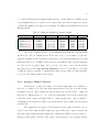
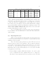
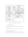

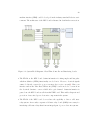
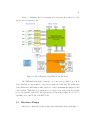
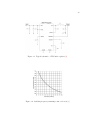
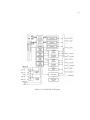
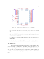
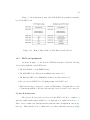
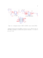
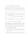
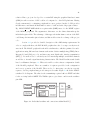
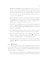
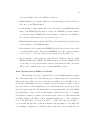
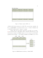
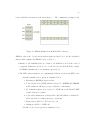
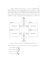
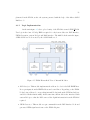
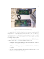
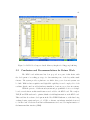
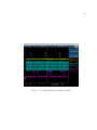


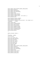

![View full document [PDF 2.57 MB]](http://vs1.manualzilla.com/store/data/006374774_1-e98d1a98aaa1be6ff2fb7da87afe8418-150x150.png)