1
®
UltraSPARC IV Processor
User’s Manual Supplement
Version 1.0
April 2004
Copyright © 2004 Sun Microsystems, Inc., 4150 Network Circle, Santa Clara, California
95054, U.S.A. All rights reserved.
Sun Microsystems, Inc. has intellectual property rights relating to technology embodied in
the product that is described in this document. In particular, and without limitation, these
intellectual property rights may include one or more of the U.S. patents listed at http://
www.sun.com/patents and one or more additional patents or pending patent applications in
the U.S. and in other countries.
This document and the product to which it pertains are distributed under licenses restricting
their use, copying, distribution, and decompilation. No part of the product or of this
document may be reproduced in any form by any means without prior written authorization
of Sun and its licensors, if any.
Third-party software, including font technology, is copyrighted and licensed from Sun
suppliers.
Sun, Sun Microsystems, the Sun logo, Java, Solaris, UltraSPARC IV, UltraSPARC III Cu,
UltraSPARC, Sun Fireplane Interconnect, VIS and OpenBoot PROM are trademarks or
registered trademarks of Sun Microsystems, Inc. in the U.S. and other countries.
All SPARC trademarks are used under license and are trademarks or registered trademarks of
SPARC International, Inc. in the U.S. and other countries. Products bearing SPARC
trademarks are based upon architecture developed by Sun Microsystems, Inc.
DOCUMENTATION IS PROVIDED "AS IS" AND ALL EXPRESS OR IMPLIED
CONDITIONS, REPRESENTATIONS AND WARRANTIES, INCLUDING ANY IMPLIED
WARRANTY OF MERCHANTABILITY, FITNESS FOR A PARTICULAR PURPOSE OR
NON-INFRINGEMENT, ARE DISCLAIMED, EXCEPT TO THE EXTENT THAT SUCH
DISCLAIMERS ARE HELD TO BE LEGALLY INVALID.
UltraSPARC IV Processor User’s Manual • April 2004
Table of Contents
Preface ................................................................................................................................ xi
1.
Introducing the UltraSPARC IV Processor .....................................................................1
1.1
2.
3.
Overview ................................................................................................................1
Architectural Overview .....................................................................................................3
2.1
Introduction ............................................................................................................3
2.2
New Features in the UltraSPARC IV Processor .....................................................4
2.3
RAS Architecture ...................................................................................................5
Chip Multithreading (CMT) .............................................................................................7
3.1
3.2
3.3
Introduction ............................................................................................................7
3.1.1
CMT Definition ........................................................................................7
3.1.2
General CMT Behavior ............................................................................8
Accessing CMT Registers ......................................................................................9
3.2.1
Types of CMT Registers ...........................................................................9
3.2.2
Accessing CMT Registers Through ASI Interface ...................................10
Private Processor Registers ....................................................................................10
3.3.1
LP ID Register (ASI_CORE_ID) .............................................................11
3.3.2
LP Interrupt ID Register (ASI_INTR_ID) ................................................11
3.3.3
CESR (Cluster Error Status Register) ID Register ...................................12
Table of Contents
i
3.4
3.5
3.6
Disabling and Suspending Logical Processors ...................................................... 13
3.4.1
LP Available Register (ASI_CORE_AVAILABLE) ................................. 13
3.4.2
Enabling and Disabling Logical Processors ............................................. 14
3.4.3
Suspending and Running Logical Processors .......................................... 16
Reset Handling ...................................................................................................... 20
3.5.1
Private Resets (SIR and WDR Resets) ..................................................... 20
3.5.2
Full-CMT Resets (System Reset) ............................................................ 20
3.5.3
Partial CMT Resets (XIR Reset) .............................................................. 20
Private and Shared Registers Summary ................................................................. 22
3.6.1
3.7
4.
4.1
Write Cache (W-cache) .......................................................................................... 25
4.2
External L2-Cache ................................................................................................. 27
4.2.1
L2-Cache Control Register ...................................................................... 27
4.2.2
Shared L2-Cache Configuration and Timing Control Register ................ 29
4.2.3
Secondary L2-Cache Control Register ..................................................... 30
4.2.4
2-Way Support in L2-Cache Data/ECC
Fields R/W ............................................................................................... 30
4.2.5
Direct L2-Cache Tag Bank Access and Displacement Flush ................... 32
ASI Access to L2-Cache Tag ECC Bits ................................................................. 35
Reset, RED_state, and Error_state .................................................................................. 37
5.1
Machine States After Reset ................................................................................... 37
6.
Performance Instrumentation .......................................................................................... 43
7.
Assembly Language ........................................................................................................... 45
7.1
8.
ii
CMT Register Changes Due to Reset .................................................................... 24
Caches and Cache Coherency ........................................................................................... 25
4.3
5.
Implementation Registers ........................................................................ 22
Prefetch Instruction ............................................................................................... 45
Memory Controller ............................................................................................................ 47
UltraSPARC IV Processor User’s Manual • April 2004
9.
8.1
SDRAM Timing Control ........................................................................................47
8.2
Chip-Kill DIMM Support .......................................................................................49
IEEE 754-1985 Standard ...................................................................................................51
9.1
9.2
Introduction ............................................................................................................51
9.1.1
Floating-Point Operations ........................................................................51
9.1.2
Rounding Mode ........................................................................................52
9.1.3
Nonstandard Floating Point Operating Mode ...........................................52
9.1.4
Memory and Register Data Images ..........................................................52
9.1.5
Subnormal Operations ..............................................................................52
9.1.6
FSR.CEXC and FSR.AEXC Updates .......................................................53
9.1.7
Prediction Logic .......................................................................................53
Floating-Point Numbers .........................................................................................53
9.2.1
9.3
9.4
Floating-Point Number Line ....................................................................55
IEEE Operations ....................................................................................................55
9.3.1
Addition ...................................................................................................56
9.3.2
Subtraction ...............................................................................................57
9.3.3
Multiplication ...........................................................................................58
9.3.4
Division ....................................................................................................59
9.3.5
Square Root ..............................................................................................60
9.3.6
Compare ...................................................................................................60
9.3.7
Precision Conversion ................................................................................61
9.3.8
Floating-point to Integer Number Conversion ..........................................62
9.3.9
Integer to Floating-point Number Conversion ..........................................63
9.3.10
Copy/Move Operations ............................................................................63
9.3.11
f Register Load/Store Operations .............................................................64
9.3.12
VIS Operations .........................................................................................64
Traps and Exceptions .............................................................................................64
9.4.1
Summary of Exceptions ...........................................................................66
9.4.2
Trap Event ................................................................................................66
Table of Contents
iii
9.4.3
9.5
9.6
9.7
9.8
9.9
10.
IEEE Traps ............................................................................................................ 67
9.5.1
IEEE Trap Enable Mask (TEM) ............................................................... 67
9.5.2
IEEE Invalid (nv) Trap ............................................................................. 67
9.5.3
IEEE Overflow (of) Trap ......................................................................... 67
9.5.4
IEEE Underflow (uf) Trap ....................................................................... 68
9.5.5
IEEE Divide-by-Zero (dz) Trap ............................................................... 68
9.5.6
IEEE Inexact (nx) Trap ............................................................................ 68
Underflow Operation ............................................................................................. 69
9.6.1
Trapped Underflow .................................................................................. 69
9.6.2
Untrapped Underflow ............................................................................... 70
IEEE NaN Operations ............................................................................................ 70
9.7.1
Signaling and Quiet NaNs ....................................................................... 71
9.7.2
SNaN to QNaN Transformation ............................................................... 71
9.7.3
Operations with NaN Operands ............................................................... 71
9.7.4
NaN Results from Operands without NaNs ............................................. 73
Subnormal Operations ........................................................................................... 73
9.8.1
Response to Subnormal Operands ........................................................... 73
9.8.2
Subnormal Number Generation ............................................................... 74
Conditions for Software Trapping ......................................................................... 76
Error Handling .................................................................................................................. 77
10.1
iv
Trap Priority ............................................................................................ 67
Error Handling in UltraSPARC IV Processors ....................................................... 77
10.1.1
Error Reporting Specific to a Logical Processor ...................................... 77
10.1.2
Shared Resource Error Reporting ............................................................ 79
10.1.3
Listing of CMT Errors ............................................................................. 81
UltraSPARC IV Processor User’s Manual • April 2004
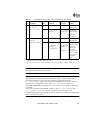
List of Tables
TABLE 2-1
Enhancements to the UltraSPARC IV Processor’s Core
..........................................................4
TABLE 2-2
Changes Due to CMT Enhancement
TABLE 3-1
LP ID Register
TABLE 3-2
LP Interrupt ID Register Fields
TABLE 3-3
CESR ID Register
TABLE 3-4
LP Available Register (Shared)
TABLE 3-5
LP Enable Status Register (Shared)
TABLE 3-6
LP Enable Register (Shared)
TABLE 3-7
LP Running Register (Shared)
TABLE 3-8
LP Running Status Register (Shared)
TABLE 3-9
XIR Steering Register (Shared)
TABLE 3-10
UltraSPARC IV Processor Private Registers
............................................................................22
TABLE 3-11
UltraSPARC IV Processor Shared Registers
............................................................................22
TABLE 4-1
Data Cache Unit Control Register
TABLE 4-2
L2-Cache Control Register
TABLE 4-3
L2-Cache Configuration and Timing Control Register
TABLE 4-4
4 MB Direct-Mapped
TABLE 4-5
4MB 2-Way Direct Mapped
TABLE 4-6
8 MB Direct-Mapped
TABLE 4-7
8 MB 2-Way Direct Mapped
........................................................................................5
........................................................................................................................11
................................................................................................12
...................................................................................................................13
...............................................................................................14
.........................................................................................15
....................................................................................................15
.................................................................................................17
.......................................................................................19
...............................................................................................21
............................................................................................25
......................................................................................................28
.............................................................29
..............................................................................................................31
....................................................................................................31
..............................................................................................................31
...................................................................................................32
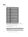
List of Tables
v
vi
TABLE 4-8
4 MB Direct-Mapped
..............................................................................................................32
TABLE 4-9
4 MB 2-way Direct-Mapped
TABLE 4-10
8 MB Direct-Mapped
TABLE 4-11
8 MB 2-Way Direct Mapped
TABLE 4-12
4 MB L2-cache Tag/State Access Data Format
........................................................................34
TABLE 4-13
8 MB L2-cache Tag/State Access Data Format
........................................................................34
TABLE 4-14
4 MB and 8 MB L2-Cache Tag/State Access Data Format
TABLE 5-1
UltraSPARC IV Processor New Defined Private Register/Field Reset Machine State
TABLE 5-2
UltraSPARC IV Defined Shared Registers/Field Reset Machine State
TABLE 6-1
Counter Behavior differences
TABLE 7-1
Prefetch Functions
TABLE 8-1
New MCU Timing Control Register
TABLE 8-2
CK_DIMM mode setting
TABLE 9-1
FSR.RD bit options
TABLE 9-2
Floating-point Numbers
..........................................................................................................53
TABLE 9-3
Floating-point Addition
...........................................................................................................56
TABLE 9-4
Floating-point Subtraction
TABLE 9-5
Floating-point Multiplication
TABLE 9-6
Floating-point Division
TABLE 9-7
Floating-point Square Root
TABLE 9-8
Number Compare
TABLE 9-9
Precision Conversion
TABLE 9-10
Floating-point to Integer Number Conversion
.........................................................................62
TABLE 9-11
Integer to Floating-point Number Conversion
.........................................................................63
TABLE 9-12
Floating-point Unit Exceptions
TABLE 9-13
Response to Traps
TABLE 9-14
Floating Point ↔ Integer Conversions that Generate Inexact Exceptions
....................................................................................................32
..............................................................................................................33
...................................................................................................33
......................................................35
..............38
.....................................39
..................................................................................................43
...................................................................................................................46
........................................................................................48
.........................................................................................................50
.................................................................................................................52
.......................................................................................................57
...................................................................................................58
...........................................................................................................59
.....................................................................................................60
....................................................................................................................60
..............................................................................................................61
................................................................................................66
...................................................................................................................66
UltraSPARC IV Processor User’s Manual • April 2004
.................................68
TABLE 9-15
Underflow Exception Summary
...............................................................................................70
TABLE 9-16
Results from NaN Operands
TABLE 9-17
Subnormal Handling Constants per Destination Register Precision
TABLE 10-1
EMU Error Mask Register Additional Bits
TABLE 10-2
L2-cache Error Enable Register Format
...................................................................................79
TABLE 10-3
CMT Error Steering Register (Shared)
.....................................................................................80
TABLE 10-4
Etag ECC errors
TABLE 10-5
Internal errors of the MCU
TABLE 10-6
Internal Error of the Write Cache
.............................................................................................82
TABLE 10-7
System Bus Protocol Error - Data
............................................................................................83
TABLE 10-8
Internal Errors of the DPCTL
TABLE 10-9
System Bus Protocol Errors - Transaction
TABLE 10-10
Cache Consistency Errors
TABLE 10-11
Snoop Result Errors
TABLE 10-12
Mtag Errors
TABLE 10-13
Internal errors on the PENDQ and QCTL
TABLE 10-14
Internal Errors of the TOB
.......................................................................................................87
TABLE 10-15
Internal errors of the ECU
.......................................................................................................87
TABLE 10-16
UltraSPARC IV Processor New Internal Error in TOB
....................................................................................................72
..........................................74
..............................................................................78
......................................................................................................................82
......................................................................................................82
..................................................................................................83
...............................................................................84
........................................................................................................85
................................................................................................................86
.............................................................................................................................86
................................................................................86
List of Tables
............................................................88
vii
viii
UltraSPARC IV Processor User’s Manual • April 2004
List of Figures
FIGURE 3-1
CMT Register Changes During Reset
FIGURE 9-1
Floating-point Number Line
...................................................................................... 24
.................................................................................................... 55
List of Figures
ix
x
UltraSPARC IV Processor User’s Manual • April 2004
Preface
This book contains information about the architecture and programming of the
UltraSPARC® IV processor, one of Sun Microsystems’ family of SPARC® V9 compliant
processors. This document is a supplement to the UltraSPARC III Cu Processor User’s
Manual and should be read in conjunction with that document.
This document extends the material in the UltraSPARC III Cu Processor User’s Manual. Any
material that is not referred to in this supplement remains unchanged for the UltraSPARC IV
processor.
Target Audience
This user’s manual is mainly targeted for programmers who write software for the
UltraSPARC IV processor. This user’s manual supplement contains a depository of
information that is useful to operating system programmers, application software
programmers, logic designers, and third party vendors, who are trying to understand the
architecture and operation of the UltraSPARC IV processor. This supplement is both a guide
and a reference manual for low-level programming of the processor.
Prerequisites
This user’s manual is a companion to the UltraSPARC III Cu Processor User’s Manual. The
reader of this user’s manual should be familiar with the contents of the UltraSPARC III Cu
Processor User’s Manual.
xi
Textual Usage
Fonts
Fonts are used as follows:
• Italic font is used for emphasis, assembly language terms, book titles, and the first
instance of a word that is defined. It is used for exception and trap names. Examples
include:
• “The privileged_action exception”
• fp_exception_ieee_754, unfinished_fp
• Courier font is used for register names (named bits), software examples, instruction
fields, and instruction names. Examples include:
• “The rs1 field contains...”
• PSTATE.RED, RED_state, NWINDOWS, PREFETCH, assign,
rand_out={lfsr_reg[1] & lfsr_reg[0]...}, FLUSH, RETRY
• UPPERCASE items are acronyms, instruction names, or writable register fields. Some
common acronyms are listed in the UltraSPARC III Cu Processor User’s Manual. Note:
Names of some instructions contain both upper- and lowercase letters.
• Underbar characters join words in register, register field, exception, and trap names. Note:
Such words can be split across lines at the underbar without an intervening hyphen. “This
is true whenever the integer_condition_code field...” is an example of how the underbar
characters are used.
Notational Conventions
The following notational conventions are used:
• Square brackets, [ ], indicate a numbered register in a register file. For example, r[0]
translates to register 0, indicate a bit number or colon-separated range of bit numbers
within a field. “Bits FSR[29:28] and FSR[12] are...”.
• Curly braces, {}, indicate textual substitution. For example, the string
“PRIMARY{_LITTLE}” expands to “ASI_PRIMARY” and “ASI_PRIMARY_LITTLE.”
• If a bar, |, is used with the curly braces, it represents multiple substitutions. For example,
the string “ASI_DMMU_TSB_{8KB|64KB|DIRECT}_PTR_REG” expands to
“ASI_DMMU_TSB_8KB_PTR_REG”, “ASI_DMMU_TSB_64KB_PTR_REG”, and
“ASI_DMMU_TSB_DIRECT_PTR_REG”.
• The
symbol designates concatenation of bit vectors. A comma (,) on the left side of an
assignment separates quantities that are concatenated for the purpose of assignment. For
example, if X, Y, and Z are 1-bit vectors and the 2-bit vector T equals 112, then
xii
UltraSPARC IV Processor User’s Manual • April 2004
(X, Y, Z) ← 0
T
results in X = 0, Y = 1, and Z = 1.
• “A mod B” means “A modulus B”, where the calculated value is the remainder when A is
divided by B.
Notation for Numbers
Numbers throughout this specification are decimal (base-10) unless otherwise indicated.
Numbers in other bases are followed by a numeric subscript indicating their base (for
example, 10012, FFFF 000016). In some cases, numbers may be preceded by “0x” to indicate
hexadecimal (base-16) notation (for example, 0xFFFF.0000). Long binary and hexadecimal
numbers within the text have spaces or periods inserted every four characters to improve
readability.
The notation 7h’1F indicates a hexadecimal number of 1F16 with 7 binary bits of width.
Informational Notes
This guide provides several different types of information in notes, as follows:
Programming Note – Programming notes contain incidental information about
programming the UltraSPARC IV processor unless otherwise restricted to a
particular processor in the family.
Implementation Note – Implementation notes contain information that contains
implementation specific information to the UltraSPARC IV processor compared to
other UltraSPARC processors.
Compatibility Note – Compatibility notes contain information relevant to the
previous SPARC-V8 architecture.
Note – This highlights a useful note regarding important and informative processor
architecture or functional operation. This may be used for purposes not covered in
one of the other notes.
Preface
xiii
xiv
UltraSPARC IV Processor User’s Manual • April 2004
CHAPTER
1
Introducing the UltraSPARC IV
Processor
Chapter Topics
1.1
• Overview on page 1
Overview
The UltraSPARC IV processor is derived from Sun Microsystems high-end UltraSPARC III
processor, providing the same fundamental features, and offering the advantage of high
throughput utilizing Chip Multithreading (CMT) technology. The UltraSPARC IV processor
features two cores, each based on the UltraSPARC III processor. From the software
perspective, the UltraSPARC IV processor appears as two software-visible logical
processors. It implements both the full 64-bit, SPARC-V9 architecture and version 2.0 of Sun
Microsystems’ VIS™ instruction set. The VIS instruction set provides a wide range of
“Single Instruction, Multiple Data” (SIMD) acceleration functions for working with 8-, 16-,
and 32-bit data values, pixel manipulation, 2D image processing, 3D graphics, data
compression, and other specialized performance-critical operations.
In common with all other members of the UltraSPARC III processor family, the
UltraSPARC IV processor is a 4-way superscalar processor, meaning it attempts to fetch 4
instructions at a time from the L1 instruction cache, and (given the appropriate instruction
mix) is capable of sustaining an execution rate of 4 instructions per clock cycle. Each
instruction is processed through a 14-stage pipeline that starts with address generation and
ends with the final retirement of any valid execution result. A 16-entry instruction queue
decouples instruction fetch from instruction issue, working to buffer any discrepancies
1-1
between these two rates. Thus, if more instructions are fetched than can be issued repeatedly,
an empty instruction queue gradually will fill. Or, if the next instruction fetch misses in the
L1 cache, a filled instruction queue can hide this break in the flow of instructions through the
pipeline, by continuing to supply the execution units with instructions for the several clock
cycles needed to retrieve the missing block of instructions from the integrated L2 cache.
To enhance throughput, while instructions enter and exit the instruction queue in strict
program order, they can complete executing out-of-order. For example, if a short latency
instruction (like an integer add) follows a long latency instruction (like an integer divide) in
the pipeline, the fast operation does not need to wait on the slow one to finish. Instructions
fetched together will enter the queue in parallel, but, within the constraints imposed by
program order, they may exit the queue in company with instructions fetched either earlier or
later (depending on the specific instruction mix and availability of the necessary functional
units).
The UltraSPARC IV processor is supported by Sun’s popular Solaris™ operating system,
providing access to the more than eight thousand applications that have been developed for
the SPARC/Solaris platform over the years. Comprehensive sets of programs are available for
many fields, including engineering, manufacturing, telecommunications, financial services,
health, retail, ecommerce, and a variety of other industry segments. Additional operating
systems available for use with UltraSPARC processors include Linux and leading real-time
operating systems. A robust set of tools for developing software also can be readily acquired,
either from Sun Microsystems or independent software vendors.
1-2
UltraSPARC IV Processor User’s Manual • April 2004
CHAPTER
2
Architectural Overview
This chapter supplements Chapter 3 of the UltraSPARC III Cu Processor User’s Manual and
contains additional information for the UltraSPARC IV processor.
Chapter Topics
2.1
• Introduction on page 3
• New Features in the UltraSPARC IV Processor on page 4
• RAS Architecture on page 5
Introduction
The UltraSPARC IV processor features two cores, each based on the UltraSPARC III
processor. From the software perspective, the UltraSPARC IV processor appears as two
software-visible logical processors. Each logical processor has access to the same size
external cache as the UltraSPARC III Cu processor, however, the UltraSPARC IV processor’s
caches have smaller lines for less contention and optimal Least Recently Used (LRU)
replacement.
The primary design goal for the UltraSPARC IV processor is to improve the performance on
commercial applications such as databases and web servers. The following three key
techniques are used to improve the UltraSPARC IV processor’s performance:
• Integrated two cores on a single processor. This technique significantly increases
throughput per cubic foot, per Watt and per dollar.
• Improved L2-cache configuration. Each logical processor has access to an 8 MB, 2-way
set associative cache. The line sizes are also reduced from 512 bytes to 128 bytes to
reduce extra contention with sub-blocked caches. In addition, a more optimal cache
replacement policy (LRU) is used.
2-3
• Enhanced Floating Point Unit and Write Cache. The write cache is enhanced with hashed
index to reduce conflict misses, especially in case of multiple write streams. This
enhancement helps codes such as high radix Fast Fourier Transform (FFT).
Executing applications share the address and data bus when accessing the L2-cache data, the
Memory Control Unit (MCU), and the SunTM Fireplane Interconnect port. The bus to the L2cache and the physical SRAM modules containing the L2-cache is shared. The two L2caches are split across 2 SRAM modules in such a fashion that both modules are used by
each cache.
This document describes only the changes for the UltraSPARC IV processor with respect to
the UltraSPARC III Cu processor. Section 2.2 summarizes all of the feature changes of the
UltraSPARC IV processor. These changes may be due to enhancing processor performance
or adopting CMT technology.
2.2
New Features in the UltraSPARC IV
Processor
This section summarizes the UltraSPARC IV processor changes with respect to the
UltraSPARC III Cu processor in TABLE 2-1 and TABLE 2-2. TABLE 2-1 lists these changes,
which includes clock rate increment and new cache organization; TABLE 2-2 lists changes
resulting from the employment of CMT technology.
TABLE 2-1
Enhancements to the UltraSPARC IV Processor’s Core
Feature
Each logical processor has access to 8 MB of L2-cache with 128-byte line size (2
sub-blocks per line) or 4 MB with 64-byte line size (no sub-block).
L2-cache employs LRU replacement strategy to increase cache hit rates.
Support L2-cache modes: 5-5-2, 5-5-3, 5-5-4, 5-5-5, 6-6-5, 6-6-6.
Support higher system frequency ratios, up to 10:1.
Low power mode is not supported.
Chip-Kill DIMM1 support allows detection and correction of DRAM chip failure.
Internal Banking support allows for more optimal DIMM scheduling.
(Only available when CK-DIMMs are used).
L2-cache Address Bus error detection for all system platforms.
2-4
UltraSPARC IV Processor User’s Manual • April 2004
TABLE 2-1
Enhancements to the UltraSPARC IV Processor’s Core
Feature
New Write cache indexing-hashing feature.
Hardware support for rare corner cases in floating point add/sub operations. Avoids
unfinished_FPop traps.
More optimal software prefetch semantics. Hardware response to the prefetch
instruction.
1. Dual Inline Memory Module (DIMM)
TABLE 2-2
Changes Due to CMT Enhancement
Feature
Some resources such as some MCU registers, some pins, and some Sun Fireplane
Interconnect registers are shared.
One new shared MCU Timing Control register is added to support a broader range of
SDRAM timing.
New registers have been added to support the Sun Standard CMT model.
Certain processor registers have been mapped to allow CMT operation.
Each logical processor has an associated CESR ID register for enhanced error
diagnostics and recovery in tightly clustered systems.
Note – In the UltraSPARC IV processor, applications can access shared registers. If
applications being executed on separate logical processors try to read/write the
same shared register at the same time, the UltraSPARC IV processor will arbitrate
and sequence the requests. However, the order is not guaranteed. To obtain a
deterministic result, the software must program it correctly, e.g., by using “mutex”
semantics.
2.3
RAS Architecture
The UltraSPARC IV processor inherits all of the RAS (Reliability, Availability and
Serviceability) features implemented in the UltraSPARC III Cu processor with the following
differences and enhancements:
Architectural Overview
2-5
The UltraSPARC IV Processor Adds Chip-Kill DIMM Support
In addition to NG-DIMM, the UltraSPARC IV processor also supports Chip-Kill SDRAM
DIMM (CK-DIMM). The CK-DIMM employs x4 SDRAM parts. Each bit of an SDRAM is
protected by different Error Correction Code bits. Therefore, the system can correct errors
resulting from one failed SDRAM.
The UltraSPARC IV Processor Adds L2-cache Address Bus Error Detection
Capability
In the UltraSPARC III Cu processor, two sets of address and control signals are used to
read/write the L2-cache data: one for the lower 16 bytes of data and its corresponding ECC;
the other for the upper 16 bytes of data and the corresponding ECC. In the UltraSPARC IV
processor, the same two sets of address and control signals are maintained. However, the set
of signals that accesses the lower 16 bytes of data now accesses the ECC of the upper 16
bytes of data, and the set of signals that accesses the upper 16 bytes of data now accesses the
ECC of the lower 16 bytes of data. By splitting the ECC this way, the address buses used to
access the L2-cache are implicitly protected.
2-6
UltraSPARC IV Processor User’s Manual • April 2004
CHAPTER
3
Chip Multithreading (CMT)
The UltraSPARC IV processor supports Sun’s new software interface and registers to support
logical processor identification, reset, diagnostics, and error reporting. These CMT registers
can be classified as private or shared.
Chapter Topics
3.1
•
•
•
•
•
•
•
Introduction on page 7
Accessing CMT Registers on page 9
Private Processor Registers on page 10
Disabling and Suspending Logical Processors on page 13
Reset Handling on page 20
Private and Shared Registers Summary on page 22
CMT Register Changes Due to Reset on page 24
Introduction
This chapter corresponds to Sun’s common interface between hardware and software and
addresses issues common to CMT processors.
3.1.1
CMT Definition
A CMT processor is defined by its external visible nature and not its internal organization.
The following section provides background terminology followed by a description of the
CMT definition.
3-7
3.1.1.1
Background Terminology
Thread
The basic unit of program execution; a stream of computer instructions that is in control of a
process.
Logical Processor (LP)
The abstraction of a processor’s architecture that maintains the state and management of an
executing thread.
Core
A hardware unit that instantiates one or more logical processors.
Processor
A single piece of silicon that interprets and executes operating system functions and other
software tasks. A processor is implemented by one or more cores.
Chip Multithreading (CMT)
A processor capable of executing 2 or more software threads simultaneously without
resorting to a software context switch. Chip Multithreading may be achieved through the use
of multiple processor cores, supporting multiple threads per core, or a combination of these
strategies.
3.1.2
General CMT Behavior
In general, each logical processor of a CMT processor behaves functionally, from the
viewpoint of software visibility, as if it was an independent unit. This is an important aspect
of CMT because user code running on a logical processor need not know whether or not that
logical processor is part of a CMT device. The operating system exploits logical processors
to simultaneously schedule multiple threads of execution. Various low-level software – boot,
error, diagnostic, among others – must be aware of multiple logical processors. This chapter
describes mainly the interface between low-level software and multiple logical processors.
Logical processors obey the same memory model semantics as if they were independent
processors. All multiprocessing libraries, thread libraries and code will be able to operate on
multiple logical processors without any modification.
3-8
UltraSPARC IV Processor User’s Manual • April 2004
Note – All previous documentation including the UltraSPARC III Cu Processor User’s
Manual and The SPARC Architecture Manual, Version 9 use the term processor. When
these earlier documents are read in conjunction with this supplement, replace the
term processor with logical processor to read them in context of the UltraSPARC IV
processor.
3.2
Accessing CMT Registers
A key part of the CMT Programming Model is a set of specific, privileged registers. This
section covers how these registers are organized and accessed. These registers can be
accessed by software running on each of the logical processors.
The CMT-specific registers, private or shared, can be accessed by privileged software
running on one of the logical processors as ASI-mapped registers. The SPARC instruction set
provides a convenient way to map an additional architectural state through the use of address
space identifiers (ASIs). This state is accessible through special load and store instructions
that provide an ASI value and an address (virtual address). Certain address space identifier
values are used to access main memory but with different behaviors than the default
semantics of normal load and store operations. Other ASI values are used to access special
state for configuration, diagnostics, or other uses. The CMT Programming Model defines a
number of ASIs specifically for accessing the CMT-specific registers.
3.2.1
Types of CMT Registers
The two main classes of CMT-specific registers are: private registers and shared registers.
• Private registers: a private copy of the register is associated with each logical processor.
• Shared registers: a single copy of each register is shared by all the logical processors.
Both private and shared registers can be accessed as ASI-mapped registers by privileged
software running on one of the logical processors. Software can access the private registers
as well as the shared registers. Each logical processor can access only its own private
registers. It cannot access the private registers of another logical processor as there is no way
to address those registers. The specific semantics for accessing the CMT registers through the
ASI interface are described in Section 3.2.2, “Accessing CMT Registers Through ASI
Interface”.
Chip Multithreading (CMT)
3-9
3.2.2
Accessing CMT Registers Through ASI Interface
Each CMT-specific register is accessible through an ASI address – a combination of an
address space identifier value and virtual address. All CMT registers are mapped into ASI
values that are only accessible in privileged mode. The specific ASI number and virtual
address of each CMT register is covered later in this document.
Each logical processor can access the private registers associated with that logical processor.
Accesses to these registers follow the standard semantics for accessing ASI mapped internal
registers.
Each logical processor can access all the shared registers. An update to a shared register from
one logical processor will be visible to all other logical processors. The ordering of accesses
to shared registers from different logical processors is not defined, but there are a number of
hardware rules that are enforced:
• The hardware guarantees that accesses to a shared register from the same logical
processor follow sequential semantics.
• The hardware also guarantees that if multiple logical processors attempt to store to the
register at the same time, after the updates, the register contains the value from one of
those stores. That is, stores to these registers must be performed atomically on all bits of
the register.
All the CMT registers are 64-bit registers, although some of the bits of individual registers
can be reserved or defined to a fixed value. Reserved register fields should always be written
by software with values of those fields previously read from that register or with zeroes; they
should read as zero in hardware. Software intended to run on future versions of CMTs should
not assume that these fields will read as 0 or any other particular value. This software
convention makes future expansion of the interface easier.
Only the LDXA, LDDFA, STXA, and STDFFA instructions can be used to access the CMT
registers. Only the Load extended from alternate space (LDXA) or Load double floating-point
register from alternate space (LDDFA) instructions can be used to read CMT registers. Only
the Store extended into alternate space (STXA) and the Store double floating-point register to
alternate space (STDFA) instructions can be used to store to CMT registers. An attempt to
access a CMT register with any other instruction results in a data_access_exception trap.
3.3
Private Processor Registers
There are three private registers used for logical processor identification.
3-10
UltraSPARC IV Processor User’s Manual • April 2004
3.3.1
LP ID Register (ASI_CORE_ID)
The LP ID register is a read-only, private register that holds the ID value assigned by
hardware to each implemented logical processor. The ID value is unique within the CMT.
The LP ID register corresponds to a bit offset for corresponding bit mask CMT registers (like
LP Enable register). Many of the CMT-specific registers provide a bit mask wherein each bit
corresponds to an individual logical processor. For these registers, the LP ID field indicates
which bit of a bit mask corresponds to a specific logical processor.
Name: ASI_CORE_ID
ASI 0x63, VA[63:0] == 0x10,
Read-Only, Privileged Access, JTAG Accessible
As described in the TABLE 3-1, the LP ID register has two fields.
TABLE 3-1
3.3.2
LP ID Register
Bit
Field
Description
[63:22]
Reserved
Reserved
[21:16]
MAX_LP_ID
Max LP ID, which gives the logical
processor ID value of the highest
numbered implemented, but not
necessarily enabled, logical processor in
this CMT processor. For the UltraSPARC IV
processor, the value of this field is 1
because there are two logical processors.
[15:6]
Reserved
Reserved
[5:0]
LP_ID
A LP ID field, which represents this
logical processor’s number, as
assigned by the hardware. The LP ID
is encoded in 6-bits. In the
UltraSPARC IV processor, one logical
processor has a value of 6’b000000; the
other logical processor has a value of
6’b000001.
LP Interrupt ID Register (ASI_INTR_ID)
The LP Interrupt ID register, described in TABLE 3-2, is added to support the Sun Fireplane
Interconnect interrupt transaction. This register is used to differentiate to which logical
processor the interrupt is sent. This private register is used by software to assign a 10-bit
interrupt ID to a logical processor that is unique within the system. This is important to
enable logical processors to receive interrupts. The ID in this register is used by other logical
processors and other bus agents to address interrupts to this specific logical processor. It is
Chip Multithreading (CMT)
3-11
also used by this logical processor to identify the source of interrupts it issues to other
logical processors and bus agents. It is expected to be changed only at boot or
reconfiguration time.
Name: ASI_INTR_ID
ASI 0x63, VA[63:0] == 0x00,
Read-Write, Privileged Access
Note – The UltraSPARC IV processor sets the Sun Fireplane MID[9:5] to SID_U and
MID[4:0] to SID_L. The source of MID[9:0] is the ASI_INTR_ID[9:0] of the logical
processor issuing the INT.
TABLE 3-2
LP Interrupt ID Register Fields
Bits
Field
Description
[63:10]
Reserved
Reserved.
[9:0]
Int ID
The Int ID is used as the source or target logical processor
identities in a Sun Fireplane Interconnect INT transaction.
In a Sun Fireplane Interconnect INT transaction, the source
logical processor identity is placed in the Sun Fireplane
Interconnect Address bus bits [38:29], and the target logical
processor identity is placed in Address bus bits [23:14].
Note – If the Int ID of the two logical processors in an UltraSPARC IV processor are
not unique in a system, then the behavior of the logical processor when an interrupt
specifying that ID is sent or received is undefined.
3.3.3
CESR (Cluster Error Status Register) ID Register
The CESR ID register, summarized in TABLE 3-3, provides support for a tightly clustered
system. This register contains an 8-bit field, CESR ID, which uniquely identifies a logical
processor in a tightly clustered system. Certain transactions append this value into the
transaction. This allows software at a remote node or within the cluster switch to associate
the initiating logical processor with the transaction.
The CESR ID register should only be used with the appropriate cluster interconnect and the
corresponding cluster specific software support. The specific value to encode in the
CESR ID register is platform−specific. When not used in a cluster architecture, this register
should always be programmed to zero.
3-12
UltraSPARC IV Processor User’s Manual • April 2004
Name: ASI_CESR_ID
ASI 0x63, VA[63:0]==0x40,
Read-Write, Privileged Access
TABLE 3-3
CESR ID Register
Bit
Field
Description
[63:8]
Reserved
Reserved
[7:0]
CESR ID
The CESR ID field is an 8-bit CESR ID in
the bus transaction. For a RBIO/WBIO
transaction, CESR[7:0] is encoded
appropriately.
Note – The CESR_ID only affects the Sun Fireplane Interconnect RBIO and WBIO
transactions. It does not affect other types of Sun Fireplane Interconnect transactions.
3.4
Disabling and Suspending Logical
Processors
The CMT programming model provides the ability to disable or temporarily suspend logical
processors. This section describes the interface for probing which logical processors are
available, enabled, and not suspended. This section also describes the interface for enabling/
disabling and suspending/running logical processors. The registers described in this section
are shared between logical processors.
3.4.1
LP Available Register (ASI_CORE_AVAILABLE)
The LP Available register is a shared register that indicates the number of logical processors
implemented in a CMT processor and which logical processor numbers are assigned to them.
Name: ASI_CORE_AVAILABLE
ASI 0x41, VA[63:0]==0x00,
Read-Only, Privileged
The LP Available register is a read-only register with fields in which each bit position
corresponds to a logical processor. Bit [0] represents LP 0; bit [1] represents LP 1.
Chip Multithreading (CMT)
3-13
If a bit position in the register is asserted (1), the corresponding logical processor is
implemented and is functional in the CMT processor. If a bit position in the register is not
asserted (0), the corresponding logical processor is not implemented or was permanently
disabled at manufacturing time. An implemented logical processor is a logical processor that
can be enabled and used.
In the UltraSPARC IV processor, this register is always read as 2’b11.
TABLE 3-4 shows the format of the LP Available register. Each bit represents one logical
processor: bit 0 for LP 0, bit 1 for LP 1, and so on. If a logical processor is available (or
implemented), then the hardware will set the corresponding bit 1. Otherwise, the hardware
sets bit 0. In the UltraSPARC IV processor, bit 1 and bit 0 will be set to 1; bits [63:2] are
always 0.
TABLE 3-4
3.4.2
LP Available Register (Shared)
Bit
Field
Description
[63:2]
Reserved
Reserved. 0 when read
[1]
LP 1
This bit represents LP 1.
[0]
LP 0
This bit represents LP 0.
Enabling and Disabling Logical Processors
The CMT programming model allows logical processors to be enabled and disabled.
Enabling or disabling a logical processor is a heavyweight operation that requires a system
reset for updates. Disabled logical processors produce no architectural effects observable by
other logical processors, and do not participate in cache coherency. Any transaction issued to
a disabled logical processor, such as an interrupt, results in an “unmapped” reply or a
time-out.
3.4.2.1
LP Enable Status Register (ASI_CORE_ENABLE_STATUS)
The LP Enable Status register is a shared register that indicates whether each logical
processor is currently enabled. The register is a read-only register with a single 64-bit field
(assuming a maximum of 64 logical processors per CMT processor) in which each bit
corresponds to a possible logical processor. The UltraSPARC IV processor has only two
software-visible logical processors.
Name: ASI_CORE_ENABLE_STATUS
ASI 0x41, VA[63:0]==0x10,
Read-Only, Privileged, JTAG Accessible
3-14
UltraSPARC IV Processor User’s Manual • April 2004
Bit [0] and bit [1] represents LP 0 and LP 1, respectively. If a bit in the register is asserted
(1), the corresponding logical processor is implemented and enabled. A logical processor not
implemented in a CMT device, indicated as “not available” in the LP Available register,
cannot be enabled and its corresponding enabled bit in this register will be 0. A logical
processor that is suspended is still considered enabled.
TABLE 3-5 shows the format of the LP Enable Status register. Each bit represents one logical
processor. A bit set to 1 indicates the corresponding logical processor is enabled; if set to 0,
it is otherwise. In the UltraSPARC IV processor, bit [0] and bit [1] are defined for LP 0 and
LP 1, respectively. Bits [63:2] are reserved and read as 0.
LP Enable Status Register (Shared)
TABLE 3-5
Bit
Field
Description
[63:2]
Reserved
Reserved. Must be 0 when read
[1]
LP 1
This bit represents LP 1.
[0]
LP 0
This bit represents LP 0.
A logical processor disabled by programming the LP Enable register (it requires a power on
reset or system reset for the updates to the LP Enable register to take effect) is considered not
enabled. A logical processor suspended for debug or diagnostics is considered enabled.
State After Reset
The LP Enable Status register changes only at system resets or power on reset. The logical
processor enable status register value is set by hardware to the value of the LP Enable
register at the deassertion of reset.
3.4.2.2
LP Enable Register (ASI_CORE_ENABLE)
The LP Enable register, illustrated in TABLE 3-6, is used by software to enable/disable logical
processor(s). The enable/disable action takes effect only when a power on reset or a system
reset (Soft POR) is deasserted.
Name: ASI_CORE_ENABLE
ASI 0x41, VA[63:0]==0x20,
Privileged, Read-Write, JTAG Accessible
LP Enable Register (Shared)
TABLE 3-6
Bit
Field
Description
[63:2]
Reserved
Reserved. Must be 0 when read
[1]
LP 1
This bit represents LP 1.
[0]
LP 0
This bit represents LP 0.
Chip Multithreading (CMT)
3-15
The LP Enable register is a 64-bit register. Each bit of the register represents one logical
processor, with bit [0] representing LP 0, and bit [1] representing LP 1. A bit set to 1 means
a logical processor should be enabled after the next system reset and a bit set to 0 means a
logical processor should be disabled after the next reset. Note that bits [63:2] are forced to 0
since their corresponding logical processors are not implemented in the UltraSPARC IV
processor.
If a bit in the LP Available register is 0 (unavailable), hardware forces the corresponding bit
in the LP Enable register to 0 and ignores attempts to write “1” to that bit. Since the
UltraSPARC IV processor always has both logical processors available, this scenario does
not exist in the UltraSPARC IV processor.
Note – A disabled logical processor in the UltraSPARC IV processor will not
respond to any transaction issued to it. The sender should encounter an unmapped
reply or a timeout error.
Note – In the UltraSPARC IV processor, if both bits 1 and 0 are set to 0, then both
logical processors will be disabled after a Hard/Soft POR.
State After Reset
The value of the LP Enable register is set to the value of the LP Available register at the
assertion of a power on reset. The value of the LP Enable register remains unchanged during
all other resets, including system resets, or equivalent resets.
3.4.3
Suspending and Running Logical Processors
Suspending is a way to temporarily suspend the operation of a logical processor. Suspended
logical processors can be set to run later. The suspending and running of logical processors
can be performed at arbitrary points in time and, unlike disabling a logical processor, a
system reset is not required. There may be an arbitrarily long, but bounded, delay from when
a logical processor is directed to suspend until the change takes effect. There is a LP
Running Status register that can be used to determine if a logical processor has completed
the process of becoming suspended.
A suspended logical processor does not execute instructions and does not initiate any
transactions on its own. A suspended logical processor does remain coherent with the
system. To remain coherent, a suspended logical processor fully participates in cache
coherency and can generate transactions in response to coherency requests from other logical
processors on the same or different CMT processor. When a logical processor is set to run, it
continues execution with the instruction that was next to be executed when the logical
processor was suspended. It is transparent to the software running on a logical processor that
it was ever suspended.
3-16
UltraSPARC IV Processor User’s Manual • April 2004
An interrupt to a suspended logical processor behaves the same as if the logical processor
was too busy to accept the interrupt. For example, if an interrupt buffer is available, the
interrupt is ACK’ed and a trap is taken only when the logical processor is set to run. If,
however, no interrupt buffer is available, the interrupt is NACK’ed.
The STICK and TICK counters will continue to count while a logical processor is suspended.
Suspending logical processors is intended for critical diagnostic and recovery code. The
interference with performance monitors using the TICK or STICK counters should not be a
general issue. Using the TICK or STICK counter to detect the suspending of a logical
processor is not recommended.
3.4.3.1
LP Running Register (ASI_CORE_RUNNING)
The LP Running register is a shared register, used by software to suspend and run selected
logical processors. When a logical processor is suspended, the logical processor stops
executing new instructions and will not initiate transactions except in response to a
coherency transaction initiated by another logical processor. There may be an arbitrarily
long, but bounded, delay from when the LP Running register is updated until the
corresponding logical processor(s) actually suspends or is set to run.
The LP Running register, is described in TABLE 3-7, is used by software to suspend selected
logical processors.
Name: ASI_CORE_RUNNING_RW
ASI 0x41, VA[63:0]==0x50,
Privileged, Read-Write, JTAG Accessible
Name: ASI_CORE_RUNNING_W1S
ASI 0x41, VA[63:0]==0x60,
Privileged, Write-Only (Write-One to Set)
Name: ASI_CORE_RUNNING_W1C
ASI 0x41, VA[63:0]==0x68,
Privileged, Write-Only (Write-One to Clear)
LP Running Register (Shared)
TABLE 3-7
Bit
Field
Description
[63:2]
Reserved
Reserved. Must be 0 when read
[1]
LP 1
This bit represents LP 1.
[0]
LP 0
This bit represents LP 0.
The LP Running register is a 64-bit register. Each bit of the register represents one logical
processor, with bit [0] representing LP 0, and bit [1] representing LP 1.
Chip Multithreading (CMT)
3-17
Once a logical processor is set to suspend, the logical processor will stop fetching
instructions, complete the instructions in the logical processor and the instruction buffers,
and then become idle. When the logical processor is set to run, it continues execution from
the point it was suspended.
A logical processor is allowed to suspend itself. A logical processor that suspends itself
should follow the ASI write by a FLUSH instruction. This satisfies the ASI writing rules and
guarantees that the logical processor will be suspended and no instructions will be executed
following the FLUSH if the logical processor is successfully suspended. The FLUSH
instruction itself may be erected before or after the logical processor is suspended.
Note – The UltraSPARC IV processor will not allow software to set both logical
processors to be suspended. On an update to the LP Running register that would
cause both logical processors to become suspended, the logical processor making the
update is automatically set to run by hardware.
To minimize the need for synchronization between logical processors in writing to this
register, separate virtual addresses are provided to set and reset the bits of this register. This,
combined with the reset setting, means that the need for special interlocking on the register
is not necessary.
When writing to this register, there is a choice between writing an exact value and modifying
individual bits. When a logical processor suspends itself, a write to the clear bit VA should
be used. When a logical processor wants to become the only logical processor active, it is
more appropriate to write the desired value directly to the direct access VA. A direct write
eliminates the need to perform a set and a clear operation to write a specific value to the
register.
State After Reset
On assertion of power on reset or system reset (Soft POR), the LP Running register will be
initialized such that all the logical processors are suspended, except the logical processor
with the lowest number which is marked “enabled” in the LP Enable Status register. This
provides an integrated “boot master” logical processor for systems without a System
Controller (SC), reducing bootbus contention. In systems with a SC, the value of the LP
Running register can be changed using JTAG. In this way the SC (which is the boot master
in these systems) can be set to run the proper logical processor before removing the reset
signal. The logical processor that is suspended at the end of the reset should be set to run by
the master logical processor at the proper time in the booting process.
3.4.3.2
LP Running Status Register (ASI_CORE_RUNNING_STATUS)
Since there is a delay from when a logical processor is directed to suspend until it actually
becomes suspended, the LP Running Status register is provided to indicate when a logical
processor actually becomes suspended. The LP Running Status register is a shared, read-only
register where each bit indicates if the corresponding logical processor is active.
3-18
UltraSPARC IV Processor User’s Manual • April 2004
In the UltraSPARC IV processor, a logical processor is considered suspended successfully if
the following conditions are satisfied:
1. No instruction in the instruction queue and logical processor.
2. No pending I-cache fetch, D-cache load, D-cache store, P-cache load, and W-cache
eviction requests.
3. No requests in the Store Queue.
Note – A D-cache load is considered finished if the D-cache has received the data.
Name: ASI_CORE_RUNNING_STATUS
ASI 0x41, VA[63:0]==0x58,
Privileged, Read-Only, JTAG Accessible
LP Running Status Register (Shared)
TABLE 3-8
Bit
Field
Description
[63:2]
Reserved
Reserved. Must be 0 when read
[1]
LP 1
This bit represents LP 1.
[0]
LP 0
This bit represents LP 0.
As shown in TABLE 3-8, the LP Running Status register is a 64-bit register. Each bit of the
register represents one logical processor, with bit [0] representing LP 0, and bit [1]
representing LP 1.
For any bit set to 1 in the LP Running register, the corresponding bit needs to be 1 in the LP
Running Status register.
Note – For one suspend command to a logical processor, the corresponding bit of
the specified logical processor in the LP Running Status register will have only one
transition from 1 to 0.
Note – The LP Enable, LP Running, and LP Running Status registers are mainly
used to support debug and diagnostics. The LP Running register is also used to
support booting.
State After Reset
The value of the LP Running Status register is the same as the value of the LP Running
register at the end of a system reset.
Chip Multithreading (CMT)
3-19
3.5
Reset Handling
Each Reset is handled differently in a CMT processor. Some resets apply to all the logical
processors, some apply to an individual logical processor, and some apply to an arbitrary
subset. The following sections address how each type of reset is handled with respect to
having multiple logical processors integrated into a package. In general, the reset
nomenclature used is consistent with UltraSPARC IV processors. Future processors may
have a different classification of resets; if this is the case, the processors should extend this
model appropriately.
3.5.1
Private Resets (SIR and WDR Resets)
The only resets that are limited to a single logical processor are the private resets internally
generated by a logical processor. An UltraSPARC IV processor has a number of resets of this
class. These types of resets are generated by an individual logical processor and are not
propagated to the other logical processors on a CMT processor.
3.5.2
Full-CMT Resets (System Reset)
There is a class of resets that are generated by an external agent and apply to all the logical
processors in a CMT processor. These include any reset that can be associated with
fundamentally reconfigure the CMT processor. Current SPARC processors have a system
reset, of which power-on reset is a special case. This is a reset that is required for certain
reconfigurations of the processor. Future processors may have multiple resets that replace the
single system reset of current processors.
The power-on and system resets (or their equivalents in future processors) are sent to all
logical processors in a CMT processor. All logical processors except the lowest enabled
logical processor are set, by default, to suspended at the beginning of system reset. The
logical processor that is set to run is the default master logical processor, which should
arbitrate for the bootbus (if multiple CMT processors share the same bootbus). The master
logical processor should run the other logical processors at the proper time in the booting
process.
3.5.3
Partial CMT Resets (XIR Reset)
There is a class of resets that are generated by an external agent and apply to an arbitrary
subset of logical processors within a CMT processor. The subset may be anything from all
logical processors to no logical processors. The UltraSPARC IV processors have, in addition
3-20
UltraSPARC IV Processor User’s Manual • April 2004
to a system reset, an additional externally initiated reset called an XIR. This is a reset
intended to reset a specific processor in a system, primarily for diagnostic and recovery
purposes. Future processors may have multiple resets that replace the single XIR reset of
current processors.
For this class of resets there must be a mechanism to specify which subset of logical
processors should be reset. There are two possible ways to specify the subset. The first way
to specify the subset is to have a steering register that is set up ahead of time to specify the
subset of logical processors. For systems using an XIR reset, the XIR Steering register
described in Section 3.5.3.1, “XIR Steering Register (ASI_XIR_STEERING)” should be
used.
The second way to specify the subset is to specify the subset concurrently with delivering the
reset across the interface used for communicating the reset. This method would require that
the interface used for communicating resets supports sending packets of information along
with the resets.
3.5.3.1
XIR Steering Register (ASI_XIR_STEERING)
The XIR reset can be steered only to specific logical processors under the control of the XIR
Steering register described in TABLE 3-9.
Name: ASI_XIR_STEERING
ASI 0x41, VA[63:0]==0x30,
Privileged, Read-Write, JTAG Accessible
XIR Steering Register (Shared)
TABLE 3-9
Bit
Field
Description
[63:2]
Reserved
Reserved. Must be 0 when read
[1]
LP 1
This bit represents LP 1.
[0]
LP 0
This bit represents LP 0.
The XIR Steering register is a 64-bit register out of which only bits [1:0] are used in the
UltraSPARC IV processor. Each bit of the register represents one logical processor, with bit
[0] representing LP 0, and bit [1] representing LP 1. An XIR is blocked to a logical processor
if the corresponding bit is 0. Hardware will force a 0 for unimplemented logical processors.
State After Reset
At the end of a system reset (or equivalent reset), the value of the XIR reset is equal to the
value of the LP Enable Status register (which in turn is equal to the value of the LP Enable
register).
Chip Multithreading (CMT)
3-21
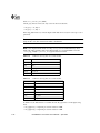
3.6
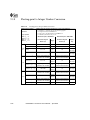
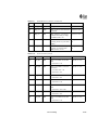
Private and Shared Registers Summary
The UltraSPARC IV processor implements the following private and shared registers.
3.6.1
Implementation Registers
TABLE 3-10 and TABLE 3-11 summarize the private and shared registers, respectively.
TABLE 3-10
UltraSPARC IV Processor Private Registers
ASI
Value
ASI Name
Access
VA
Description
JTAG
Accessible
0x63
ASI_INTR_ID
RW
0x00
Interrupt ID
register
No
0x63
ASI_CORE_ID
R
0x10
LP ID register
Yes
0x63
ASI_CESR_ID
RW
0x40
CESR ID
No
register
TABLE 3-11
3-22
UltraSPARC IV Processor Shared Registers
ASI
Value
ASI Name
Access
VA
Description
JTAG
Accessible
0x41
ASI_CORE_AVAILABLE
R
0x00
LP Available register
No
0x41
ASI_CORE_ENABLE_STATUS
R
0x10
LP Enable Status
register
Yes
0x41
ASI_CORE_ENABLE
RW
0x20
LP Enable register,
Read-Write
Yes
0x41
ASI_XIR_STEERING
RW
0x30
XIR Steering register,
Read-Write
Yes
0x41
ASI_CORE_RUNNING_RW
RW
0x50
LP Running register,
Read-Write
Yes
0x41
ASI_CORE_RUNNING_W1S
W
0x60
LP Running register,
Write One Set
-
0x41
ASI_CORE_RUNNING_W1C
W
0x68
LP Running register,
Write One Clear
-
0x41
ASI_CORE_RUNNING_STATUS
R
0x58
LP Running Status
register
Yes
0x41
ASI_CMT_ERROR_STEERING
RW
0x40
Error Steering
register, Read-Write
Yes
UltraSPARC IV Processor User’s Manual • April 2004
Note – ASI accesses to the registers must use LDXA/STXA/LDDFA/STDFA
instructions. Using another type of load or store instruction will cause a
data_access_exception trap (with SFSR.FT = 8, illegal ASI value, VA, RW, or size).
Attempt to access these registers while in non-privileged mode will cause a
privileged_action trap (with SFSR.FT = 1, privilege violation). A non-aligned access
will cause a mem_address_not_aligned trap. If the instruction is LDDFA/STDFA and if
the address is aligned to a 32-bit boundary but not to a 64-bit boundary, then the
trap type will be LDDF/STDF_mem_address_not_aligned.
Chip Multithreading (CMT)
3-23
3.7
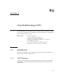
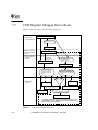
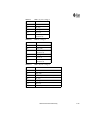
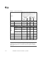
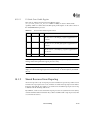
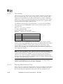
CMT Register Changes Due to Reset
FIGURE 3-1 shows the changes in CMT registers during reset.
LP_AVAILABLE
Set at time
of manufacture
encoded index of
most sig. ‘1’ bit
max_LP_id
State of running
processor before
reset
Set at beginning
of reset
LP_ENABLE
non-POR
system reset
POR
POR
non-POR
system reset
least significant ‘1’
bit remains ‘1’;
others set to ‘0’
LP_ENABLE
LP_RUNNING
During reset
value is unchanged by
processor, but may be
changed by an external
agent*
Set at end
of reset
value is unchanged by
processor, but may be
changed by an external
agent*
LP_RUNNING
LP_ENABLE
LP_ENABLE_STATUS
LP_RUNNING_STATUS
encoded index of
least significant ‘1’ bit
XIR_STEERING
LP_ERROR_STEERING
* If modification of this value by an external agent causes it to be
incompatible with other logical processor states, logical processor
behavior after reset is undefined.
FIGURE 3-1
3-24
CMT Register Changes During Reset
UltraSPARC IV Processor User’s Manual • April 2004
CHAPTER
4
Caches and Cache Coherency
This chapter supplements Chapter 10 of the UltraSPARC III Cu Processor User’s Manual
and contains additional information for the UltraSPARC IV processor. All registers described
in this chapter are private unless otherwise specified.
Chapter Topics
4.1
• Write Cache (W-cache) on page 25
• External L2-Cache on page 27
Write Cache (W-cache)
To reduce W-cache miss rates for certain classes of applications, such as radix-8 FFT, the
UltraSPARC IV processor adds an option that uses hashed index to access the W-cache. This
feature is controlled on a logical processor basis by the WIH bit in the Data Cache Unit
Control Register (ASI 0x45, VA 0x00), illustrated in TABLE 4-1.
Name: ASI_DCU_CONTROL_REGISTER
ASI 0x45, VA[63:0] == 0x00,
Read-Write
TABLE 4-1
Data Cache Unit Control Register
Bit
Field
[63:50]
Reserved
[49]
CP
[48]
CV
[47]
ME
[46]
RE
4-25
TABLE 4-1
Data Cache Unit Control Register (Continued)
Bit
Field
[45]
PE
[44]
HPE
[43]
SPE
[42]
SL
[41]
WE
[40:33]
PM
[32:25]
VM
[24]
PR
[23]
PW
[22]
VR
[21]
VW
[20:5]
Reserved
[4]
WIH
[3]
DM
[2]
IM
[1]
DC
[0]
IC
The following occurs if the WIH bit 4 is set to:
• 0 = Use PA[8:6] for index selection
• 1 = Use the hash function, PA[8:6] ^ PA[11:9] ^ PA[14:12] ^ PA[17:15], for index
selection (where ^ is bit-wise exclusive OR).
Note – WIH is used only if the WE is set.
Note – It is required to flush the W-cache and store buffer before changing the WIH
setting. This may require disabling interrupt and using MEMBAR before and after
the WIH setting instruction.
4-26
UltraSPARC IV Processor User’s Manual • April 2004
Note – The following lists a way of flushing W-cache:
1) Use ASI_WCACHE_TAG (ASI 0x3A, VA 0x0) to get W-cache line addresses.
2) For each W-cache line, calculate its L2-cache index, and apply L2-cache
Displacement Flush (ASI 0x4E, VA[24] = 1) to this index.
4.2
External L2-Cache
The external L2-cache changes described here are due to the following:
• The UltraSPARC IV processor provides support for a high processor clock rate
• The UltraSPARC IV processor L2-cache uses LRU replacement strategy
• The two software-visible logical processors in an UltraSPARC IV processor share the
same physical SRAM modules, i.e. the same physical address/data bus
The L2-cache Tag Array ECC protection mechanism, ECC algorithm, and error reporting
method in the UltraSPARC IV processor are the same as those in the UltraSPARC III Cu
processor.
Since the two software visible logical processors in an UltraSPARC IV processor share the
same physical L2-cache data memory, only one copy is needed for the cache configuration
and timing control parameters. These parameters include EC_assoc, addr_setup,
trace_out, trace_in, EC_turn_rw, EC_early, EC_size, and EC_clock. The
UltraSPARC IV processor defines a new shared register, accessed by
ASI_ECACHE_CFG_TIMING_CTRL, for these parameters. Thus, those fields in the register
accessed by ASI_ECACHE_CTRL become unused.
Note – In the UltraSPARC IV processor, the physical memory for cache data is
divided into two parts: one for LP 0; the other for LP 1. If it is accessed by LP 0, then
ex_addr[22] is always equal to 0; on the other hand, if it is accessed by LP 1, then
ex_addr[22] is always equal to 1.
The UltraSPARC IV processor supports 6-6-5 and 6-6-6 L2-cache modes, in addition to the
UltraSPARC III Cu processor modes.
4.2.1
L2-Cache Control Register
As mentioned before, the L2-cache Control register, described in TABLE 4-2, is the same as
the register accessed by ASI_ECACHE_CTRL in the UltraSPARC III Cu processor except
that the EC_assoc, addr_setup, trace_out, ZZ, trace_in, EC_turn_rw,
Caches and Cache Coherency
4-27
EC_early, EC_size, and EC_clock fields are removed. The bits for these fields are
reserved in the UltraSPARC IV processor. Writing to bits [23:11] has no effect; reading
returns an undefined value. Other fields (bits [63:25], [10:0]) have the same definitions and
access restrictions as in the UltraSPARC III Cu processor.
Bit 24, EC_FIXED_PRE_ARB, is a new defined bit in the UltraSPARC IV processor that
indicates which priority scheme should be employed in the L2-cache unit pre-arbiter for each
logical processor. Each logical processor has multiple request queues to access the L2-cache.
The arbitration between these request queues for each logical processor is decided by the
pre-arbiter for that logical processor. If the EC_FIXED_PRE_ARB bit is set to 1, a fixed
priority scheme is selected by the pre-arbiter for that logical processor. If
EC_FIXED_PRE_ARB is set to 0 (default), then a “round-robin + fixed” priority scheme is
used.
A simple distributed fair arbitration algorithm is used between the two software visible
logical processors of the UltraSPARC IV processor, to ensure that each logical processor gets
access to L2-cache. A token is passed between the two software visible logical processors. If
a logical processor has the token and the other logical processor has pending requests, the
logical processor with the token will complete its current request (if any) and hands the token
to the requesting logical processor. In this way, if only one logical processor has requests it
will hold the token and complete its requests. If both logical processors have requests, the
token will bounce back and forth with each logical processor completing single requests
when it receives the token.
Name: ASI_ECACHE_CTRL
ASI 0x75, VA[63:0] == 0x0,
Read-Write
TABLE 4-2
4-28
L2-Cache Control Register
Bit
Field
[63:27]
Reserved
[26]
pf2_RTO_en
[25]
EC_TCC_en
[24]
EC_FIXED_PRE_ARB
[23:11]
Reserved
[10]
EC_ECC_en
[9]
EC_ECC_force
[8:0]
EC_check
UltraSPARC IV Processor User’s Manual • April 2004
4.2.2
Shared L2-Cache Configuration and Timing Control
Register
The UltraSPARC IV processor L2-cache configuration and timing is controlled by the L2Cache Configuration and Timing Control register defined below, described in
TABLE 4-3. Therefore, both logical processors in the UltraSPARC IV processor will have the
same L2-cache configuration and timing. In this register, writing to the reserved bits has no
effect; reading them returns 0. Software should not program a field with “reserved” values;
Doing so will result in undefined hardware behavior.
Name: ASI_ECACHE_CFG_TIMING_CTRL
ASI 0x73, VA[63:0] == 0x00 (new assigned)
Read-Write
TABLE 4-3
L2-Cache Configuration and Timing Control Register
Bits
Field
Description
[63:25]
Reserved
Reserved.
[24]
EC_assoc
0 = Direct-mapped L2-cache
1 = 2-way L2-cache
[23]
addr_setup
Address setup cycles prior to SRAM rising clock
edge
0 = 1 cycle
1 = 2 cycles
[22:21]
trace_out
Address trace out cycles
00 = Reserved
01 = 4 cycles
10 = 5 cycles
11 = 6 cycles
[20]
Reserved
Reserved.
[19:17]
trace_in
Data trace in cycles
000 = 2 cycles
100 = 3 cycles
001 = 4 cycles
010 = 5 cycles
011 = 6 cycles
101 = Reserved
110 = Reserved
111 = Reserved
[16]
EC_turn_rw
0 = 1 SRAM cycle between read→ write
1 = 2 SRAM cycles between read→ write (default)
[15]
EC_early
Reserved.
Caches and Cache Coherency
4-29
TABLE 4-3
L2-Cache Configuration and Timing Control Register (Continued)
Bits
Field
Description
[14:13]
EC_size
[14:13]
[14:13]
[14:13]
[14:13]
==
==
==
==
00 Reserved
01 4 MB L2-cache Size
10 8 MB L2-cache Size
11 Reserved
[12:11]
EC_clock
[12:11]
[12:11]
[12:11]
[12:11]
==
==
==
==
00 Reserved
01 Reserved
10 Selects 5:1 L2-cache clock ratio
11 Selects 6:1 L2-cache clock ratio
[10:0]
Reserved
Reserved.
Note – At Hard POR and system reset (soft POR), all L2-cache mode settings
default to 6-6-5, i.e., trace_out = “6 cycles” = 2’b11, EC_clock = "selects 6:1" = 2’b11,
and trace_in = "5 cycles" = 3’b010.
Note – Similar to the UltraSPARC III/UltraSPARC III Cu processors, specifying a
1 cycle EC_turn_rw time may cause contention on the SRAM data bus for some
L2-cache modes.
4.2.3
Secondary L2-Cache Control Register
The UltraSPARC IV processor does not support the secondary L2-cache Control register
since the UltraSPARC IV processor does not support low power modes and since this register
is solely for 1/2 low power mode and 1/32 low power mode. Writing to this register has no
effect; reading will get undefined data.
4.2.4
2-Way Support in L2-Cache Data/ECC
Fields R/W
TABLE 4-4, TABLE 4-5, TABLE 4-6 and TABLE 4-7 explains the L2-cache data access address
format.
Note – Due to the new L2-cache organization, the address and data formats may
differ from the UltraSPARC III Cu processor in the ASI access discussed in
Section 4.2.4, Section 4.2.5, and Section 4.3.
4-30
UltraSPARC IV Processor User’s Manual • April 2004
ASI 0x76 (Writing) or 0x7E (Reading), VA[63:23] == 0,
Name: ASI_ECACHE_W (0x76), ASI_ECACHE_R (0x7E)
TABLE 4-4
4 MB Direct-Mapped
Bit
Field
Description
[63:22]
Reserved
Reserved
[21:5]
EC_addr
uses a 17-bit index[21:5]
to read and write a 32byte field from the
L2-cache to and from
the L2-cache Data
Staging registers.
[4:0]
Mandatory value
should be 0’s
TABLE 4-5
4MB 2-Way Direct Mapped
Bit
Field
Description
[63:22]
Reserved
Reserved
[21]
EC_way
[20:5]
EC_addr
uses a 16-bit index[20:5] plus way select to
read and write a 32-byte field from the
L2-cache to and from the L2-cache Data
Staging registers.
[4:0]
Mandatory value
should be 0’s
TABLE 4-6
8 MB Direct-Mapped
Bit
Field
Description
[63:23]
Reserved
Reserved
[22:5]
EC_addr
uses a 18-bit index [22:5] to read and
write a 32-byte field from the L2-cache to
and from the L2-cache Data Staging
registers.
[4:0]
Mandatory value
should be 0’s
Caches and Cache Coherency
4-31
TABLE 4-7
8 MB 2-Way Direct Mapped
Bit
Field
Description
[63:23]
Reserved
Reserved
[22]
EC_way
[20:5]
EC_addr
uses a 17-bit index[21:5] plus way select to
read and write a 32-byte field from the
L2-cache to and from the L2-cache Data
Staging registers.
[4:0]
Mandatory value
should be 0’s
The size of EC_addr is determined by the EC_size field specified in Section 4.2.2 “Shared
L2-Cache Configuration and Timing Control Register” on page 4-29.
4.2.5
Direct L2-Cache Tag Bank Access and Displacement
Flush
TABLE 4-8, TABLE 4-9, TABLE 4-10 and TABLE 4-11 explains the L2-cache tag access address
format.
TABLE 4-8
Bit
Field
[63:25]
Reserved
[24]
disp_flush
[23]
Mandatory value
[22]
Reserved
[21:6]
EC_tag_addr
[5:3]
Reserved
[2:0]
Mandatory value
(should be 0)
TABLE 4-9
4-32
4 MB Direct-Mapped
4 MB 2-way Direct-Mapped
Bit
Field
[63:25]
Reserved
[24]
disp_flush
[23]
Mandatory value
(should be 0)
UltraSPARC IV Processor User’s Manual • April 2004
TABLE 4-9
4 MB 2-way Direct-Mapped
Bit
Field
[22]
Reserved
[21]
EC_way
[20:6]
EC_tag_addr
[5:3]
Reserved
[2:0]
Mandatory value
(should be 0)
TABLE 4-10
8 MB Direct-Mapped
Bit
Field
[63:25]
Reserved
[24]
disp_flush
[23]
Mandatory value
(should be 0)
[22:7]
EC_tag_addr
[6:3]
Reserved
[2:0]
Mandatory value
(should be 0)
TABLE 4-11
8 MB 2-Way Direct Mapped
Bit
Field
[63:25]
Reserved
[24]
disp_flush
[23]
Mandatory value (should be 0)
[22]
EC_way
[21:7]
EC_tag_addr
[6:3]
Reserved
[2:0]
Mandatory value (should be 0)
Caches and Cache Coherency
4-33
Name: ASI_ECACHE_TAG (0x4E)
The EC_way field is an L2-cache way select for directed read/write.
• EC_way == 0, Way 0
• EC_way == 1, Way 1
If the disp_flush field is set, it means displacement flush. If it is clear, L2-cache tag access is
performed.
Note – Displacement flush will invalidate the line and cause writeback if the line is
dirty. In this case, data return from EMU is undefined.
Note – For displacement flush, use only LDXA (STXA has NOP behavior). Since
EMU will return garbage data to the MS pipeline, it is recommended to use the
“ldxa [reg_addr]ASI_ECACHE_TAG,%g0” instruction format.
TABLE 4-12
4 MB L2-cache Tag/State Access Data Format
Bit
Field
[63:43]
Reserved
[42]
LRU
[41:21]
EC_tag
[20:3]
Reserved
[2:0]
EC_state0
TABLE 4-13
8 MB L2-cache Tag/State Access Data Format
Bit
Field
[63:43]
Reserved
[42]
LRU
[41:21]
EC_tag
[20:6]
Reserved
[5:3]
EC_state1
[2:0]
EC_state0
In TABLE 4-13, the LRU field is a 1-bit LRU bit. The EC_tag field is a 21-bit physical tag
field.
• EC_tag[41:21] == PA[41:21] of associated data for 4 MB
• EC_tag[41:22] == PA[41:22] of associated data for 8 MB
4-34
UltraSPARC IV Processor User’s Manual • April 2004
Note – In the UltraSPARC IV processor and UltraSPARC III Cu processor, PA[42] is
removed from all cache tags since in all UltraSPARC III Cu processor−based
platforms, PA[42] is always 0 for cacheable address space.
Note – When writing the L2-cache tag using direct ASI access, the correct L2-cache
tag ECC bits are also automatically generated and written to the L2-cache Tag ECC
array. To intentionally inject errors, the ECC value can be changed using direct ASI
write (see Section 4.3).
Note – Each UltraSPARC IV logical processor contains 32K LRU bits. They are
addressable by VA[20:6] (4 MB) or VA[21:7] (8 MB). The EC_way signal has no effect
on accessing the LRU bits. In direct-mapped mode, normal L2-cache accesses do not
update the LRU bits, hence, the ASI_ECACHE_TAG read should return 0 unless the
LRU bits have been updated by the ASI_ECACHE_TAG write.
4.3
ASI Access to L2-Cache Tag ECC Bits
ASI 0x4E, VA[63:24] = 0x0, VA[23] = 0x1,
• For direct-mapped L2-cache:
VA[21:6] == EC_tag_addr for 4 MB
VA[22:7] == EC_tag_addr for 8 MB
• For 2-way L2-cache:
VA[21] == EC_way, VA[20:6] == EC_tag_addr for 4 MB,
VA[22] == EC_way, VA[21:7] == EC_tag_addr for 8 MB,
VA[5:0] == 0
TABLE 4-14
4 MB and 8 MB L2-Cache Tag/State Access Data Format
Bit
Field
Description
[63:8]
Reserved
Reserved
[7:0]
ECC_value
The ECC_value field is an
8-bit ECC value written to/
read from L2-cache Tag
ECC RAM
Caches and Cache Coherency
4-35
Note – The UltraSPARC IV processor uses the same algorithm as the
UltraSPARC III Cu processor to generate L2-cache tag ECC. The signals covered by
the L2-cache tag ECC include the tag and the coherence states. The LRU bit is not
covered by the ECC.
The ECC value of zero L2-cache tag is also 0. Thus, after STXA 0x40, all lines will have
correct ECC values and will be in INVALID states.
4-36
UltraSPARC IV Processor User’s Manual • April 2004
CHAPTER
5
Reset, RED_state, and Error_state
This chapter supplements Chapter 18 of the UltraSPARC III Cu Processor User’s Manual
and contains additional information for the UltraSPARC IV processor.
Chapter Topics
5.1
• Machine States After Reset on page 37
Machine States After Reset
TABLE 5-1 and TABLE 5-2 list the states of the newly added registers and fields at hard POR
and system reset (Soft POR). These new added registers or fields are unchanged after
Watchdog Reset (WDR), External Initiated Reset (XIR), Software-Initiated Reset (SIR), or
after entering RED_state.
5-37
TABLE 5-1
UltraSPARC IV Processor New Defined Private Register/Field Reset Machine
State
No.
New Register
Field
Hard_POR
State
System Reset
(Soft POR)
1.
ASI_ECACHE_CT
RL
(0x75,
VA = 0x00)
All
0
Unchanged
Default to
direct-mapped
L2-cache
All
Undefined
Unchanged
Unused in the
UltraSPARC IV
processor
Max_LP_ID
000001
Unchanged
2 LPs per
UltraSPARC IV
processor
LP ID
000000
Unchanged
LP ID
Max_LP_ID
000001
Unchanged
2 LPs per
UltraSPARC IV
processor
LP ID
000001
Unchanged
LP ID
Undefined for
both LPs
Comments
in both LPs
2.
ASI_ECACHE_CT
RL2 (0x75, VA ==
0x08)
in both LPs
3.
ASI_CORE_ID
- LP 0
ASI_CORE_ID
- LP 1
5-38
4.
ASI_INTR_ID
All
Undefined
Unchanged
5.
ASI_ESTATE_ER
ROR_EN_REG
[22:19]
0
0
6.
ASI_CESR_ID
[7:0]
0
Unchanged
7.
ASI_DCU_CONTROL_REGISTER
WIH [4]
0
0
8
Dispatch Control
Register (ASR 18)
OBS [11:6]
0
Unchanged
UltraSPARC IV Processor User’s Manual • April 2004
Default to use
PA[8:6] to index
W-cache
TABLE 5-2
UltraSPARC IV Defined Shared Registers/Field Reset Machine State
No.
New Register
Field
Hard POR
System Reset
(Soft POR)
1.
ASI_ECACHE_CFG
_TIMING_CTRL
EC_assoc
0
Unchanged
Default to
direct-mapped
L2-cache
trace_out
11
Unchanged
Default to 6
cycles (6-6-5)
trace_in
010
Unchanged
Default to 5
cycles (6-6-5)
EC_clock
11
Unchanged
Default to 6:1
L2-cache clock
ratio
EC_size
10
Unchanged
Default to 8 MB
L2-cache
EC_turn_
rw
1
Unchanged
Default to 2
cycles
Others
0
Unchanged
(0x73, VA = 0x00)
Comments
2.
New Sun Fireplane
Interconnect Clock
Ratio in
SAFARI_CONFIG
and
SAFARI_CONFIG_
21
CLK[2],
[1:0]
0,10
Unchanged
Default to 6:1
system clock
ratio
3.
SAFARI_CONFIG2
[26:17]
= ASI_INTR_ID
[9:0] of LP 0
= ASI_INTR
_ID [9:0] of
LP 0
Default to
reflect LP 0’s
INTR_ID
4.
Mem_Timing5_CTL
All
Undefined
Unchanged
5.
Mem_Address_CTL [63]
Undefined
Unchanged
Default to
disable internal
banking
6
ASI_CORE_AVAIL
ABLE
3 (decimal)
3 (decimal)
UltraSPARC IV
processor
hardware
always sets 3
(decimal) to this
register
[63:0]
(0x41, VA = 0x00)
Reset, RED_state, and Error_state
5-39
TABLE 5-2
No.
New Register
Field
Hard POR
System Reset
(Soft POR)
7.
ASI_CORE_ENABL
E_STATUS
[63:2]
0
0
(0x41, VA = 0x10)
[1:0]
Value of
ASI_CORE_ENAB
LE[1:0] at the
time of reset
deassertion
Value of
ASI_CORE_
ENABLE[1:0]
at the time of
reset
deassertion
ASI_XIR_STEERI
NG
[63:2]
0
0
(0x41, VA = 0x30)
[1:0]
Value of
ASI_CORE_ENAB
LED[1:0] at the
time of reset
deassertion
Value of
ASI_CORE_
ENABLED[1:0
] at the time
of reset
deassertion
ASI_CORE_ENABL
E
[63:2]
0
0
63-2 are not
implemented
(0x41, VA = 0x20)
[1:0]
11
Unchanged
Both LPs are
enabled by
default. During
reset, this
register could
be overwritten
by the JTAG
controller.
ASI_CORE_RUNNI
NG
[63:2]
0
0
63-2 are not
implemented
(0x41, VA = 0x50,
0x60, 0x68)
[1:0]
Deassertion:
Deassertion:
= 01, if LP 0 is
enabled;
= 01, if LP 0
is enabled;
= 10, otherwise
= 10,
otherwise
By default, only
the lowest
enabled LP will
be running after
reset. The JTAG
controller can
overwrite this
default setting.
However, only
enabled LPs can
become
running.
8.
9.
10.
5-40
UltraSPARC IV Defined Shared Registers/Field Reset Machine State
UltraSPARC IV Processor User’s Manual • April 2004
Comments
63-2 are not
implemented
63-2 are not
implemented
TABLE 5-2
UltraSPARC IV Defined Shared Registers/Field Reset Machine State
No.
New Register
Field
Hard POR
System Reset
(Soft POR)
11.
ASI_CORE_RUNNI
NG_STATUS
[63:2]
0
0
(0x41, VA = 0x58)
[1:0]
= ASI_CORE_RUN = ASI_CORE
NING[1:0]
_RUNNING[1:
0]
0 when the
corresponding
LP is
successfully
suspended
ASI_CMP_ERROR_
STEERING
[63:1]
0
0
63-2 are not
implemented
(0x41, VA = 0x40)
[0]
Deassertion:
Deassertion:
= 0, if LP 0 is
running;
= 0, if LP 0 is
running;
= 1, otherwise
= 1,
otherwise
By default, this
register encodes
the lowest
running LP
after reset.
However, the
JTAG controller
can overwrite
the default
value.
12.
Comments
63-2 are not
implemented
1. Except for the Sun Fireplane Interconnect Clock Ratio, SAFARI_CONFIG_2 has the same reset values as the
SAFARI_CONFIG in the UltraSPARC III Cu processor.
2. Except for the INT_ID field, the SAFARI_CONFIG has the same reset values as the SAFARI_CONFIG_2 register.
Note – AFAR2 (ASI 0x4C, VA 0x8) has an unknown state after Hard POR, and is
unchanged after all other types of resets.
Note – The following UltraSPARC IV processor implementations may cause
different behavior regarding the initial state after reset for some CMT registers.
1) Final states after reset of some CMT registers are determined by the
ASI_CORE_ENABLED register. However, the UltraSPARC IV processor requires a
system reset to propagate the value of the ASI_CORE_ENABLE register to
ASI_CORE_ENABLED even though ASI_CORE_ENABLE is programmed while reset
is asserted.
2) After the assertion of Hard_POR, changes to the ASI_CORE_RUNNING and
ASI_CMP_ERROR_STEERING registers will be preserved. In other words,
considering the initial states after System reset of these two registers are unchanged
unless overwritten by JTAG.
Reset, RED_state, and Error_state
5-41
5-42
UltraSPARC IV Processor User’s Manual • April 2004
CHAPTER
6
Performance Instrumentation
This chapter supplements Chapter 14 of the UltraSPARC III Cu Processor User’s Manual
and contains additional information for the UltraSPARC IV processor.
TABLE 6-1 lists the counters that count differently in the UltraSPARC IV processor in
comparison with the UltraSPARC III Cu processor.
TABLE 6-1
Counter Behavior differences
Counter
Encoding
EC_ref
[PICL]
PIC.SL = 001100
UltraSPARC IV Processor
Behavior
UltraSPARC III Cu Processor
Behavior
Total L2-Cache references,
excluding non-cacheable and
speculative load accesses
Total L2-Cache references,
excluding non-cacheable
accesses; but including
speculative load accesses.
6-43
6-44
UltraSPARC IV Processor User’s Manual • April 2004
CHAPTER
7
Assembly Language
This chapter supplements Appendix B of the UltraSPARC III Cu Processor User’s Manual
and contains additional information for the UltraSPARC IV processor.
Chapter Topics
7.1
• Prefetch Instruction on page 45
Prefetch Instruction
The UltraSPARC III Cu processor implements ten prefetch functions whose function codes
are 0, 1, 2, 3, 4, 16, 20, 21, 22, and 23. The UltraSPARC IV processor features the following
changes:
1. Prefetch with fcn = 3 now performs the same as prefetch with fcn = 2
2. Prefetch with fcn = 23 now performs the same as prefetch with fcn = 22
3. Prefetch with fcn = 17 is added whose behavior is the same as prefetch with fcn =
3 in the UltraSPARC III Cu processor.
7-45
TABLE 7-1 summarizes the prefetch instruction behavior.
Prefetch Functions
TABLE 7-1
Prefetch Instruction
for
Several Reads
Description
Modified / New
in the
UltraSPARC IV
processor
64 bytes of data from the specified target address are
prefetched by means of an RTS transaction and
installed in both E-cache and P-cache
NO
64 bytes of data from the specified target address are
prefetched by means of an RTS transaction and
installed in the P-cache
NO
64 bytes of data from the specified target address are
prefetched and install in the L2-cache. If the
ASI_ECACHE_CTRL.pf2.RTO_en bit is set, an RTO
transaction is issued for the prefetch; otherwise, an
RTS is issued
NO
YES
(fcn = 17)
64 bytes of data from the specified target address are
prefetched by means of an RTS transaction and
installed in the E-cache
Page
Implemented as NOP
NO
a line in the P-cache is invalidated if the specified
target address is found in the P-cache. A prefetch
invalidate instruction must be followed by a
MEMBAR #sync instruction
NO
(fcn = 0, 20)
One Read
(fcn = 1, 21)
Several Writes
(fcn = 2, 22 )
One Write
(fcn = 3, 23)
Read to Nearest
Unified Cache
YES
(fcn = 4)
Prefetch Invalidate
(fcn = 16)
7-46
UltraSPARC IV Processor User’s Manual • April 2004
CHAPTER
8
Memory Controller
This chapter enhances the material described in Chapter 1 of the Secondary Document to
UltraSPARC III Cu Processor User’s Manual.
Chapter Topics
8.1
• SDRAM Timing Control on page 47
• Chip-Kill DIMM Support on page 49
SDRAM Timing Control
In the UltraSPARC III Cu processor, some of the MCU timing settings were based on
processor clock rate. Due to the clock rate increase, the UltraSPARC IV processor needs to
add one bit, the most significant bit, for each of the following 12 fields: sdram_ctl_dly,
sdram_clk_dly, rd_wait, auto_rfr_cycle, rfr_int, rd_msel_dly,
rdwr_rd_ti_dly, rd_wr_ti_dly, wr_wr_ti_dly, rdwr_rd_pi_more_dly,
addr_le_pw, and cmd_pw. The UltraSPARC IV processor adds another MCU timing
control register to accommodate these bits. This register bears the same access constraints as
other MCU timing control registers.
Name: Mem_Timing5_CTL
ASI 0x72, VA[63:0] == 0x48,
PIO Addr = SAFARI ADDRESS REG + 0x400048,
Read-Write, shared register
8-47
TABLE 8-1
New MCU Timing Control Register
Bit
Feild
[63:23]
Reserved
[22]
add_le_hold
[21]
dimm_type
[20]
addr_le_pw[3]
[19]
cmd_pw[4]
[18]
Reserved
[17]
rd_msel_dly[6]
[16]
rdwr_rd_ti_dly[6]
[15]
Reserved
[14]
rdwr_rd_ti_dly[6]
[13]
Reserved
[12]
wr_wr_ti_dly[6]
[11]
rdwr_rd_pi_more_dly[5]
[10]
sdram_ctl_dly[4]
[9]
sdram_ctl_dly[3]
[8]
auto_rfr_cycle[7]
[7]
rd_wait[5]
[6:1]
Reserved
[0]
rfr_int[9]
Except for bits 21 and 22, all other parameters have the same meaning as those in the
UltraSPARC III Cu processor except that their maximum values are 2 times that of the
UltraSPARC III Cu processor. Bit 22 is defined as follows:
addr_le_hold: Address Hold Time to Address Latch Enable
0 = 2 processor clock cycles, default
1 = 3 processor clock cycles
The reserved bits have no effect when writing, and will return 0 when reading.
Note – The UltraSPARC IV processor supports 0, 1, and 2 wait states. It does not
support 3 wait states.
8-48
UltraSPARC IV Processor User’s Manual • April 2004
Note – There is only one copy of MCU registers, including those in the
UltraSPARC III Cu processor and the new one defined in this section. These registers
can be accessed by using ASI or PIO. However, the ASI access is only available for
the logical processors that are on the same die as these registers, and the PIO access
is only available for foreign UltraSPARC IV processor agents. The UltraSPARC III Cu
processor MCU registers include 4 Memory Timing Control registers, 4 Memory
Address Decoding registers, and 1 Memory Address Control register.
Note – Using the PIO method to access the MCU registers by either of the 2 logical
processors that are on the same die as these registers will result in undefined
behavior.
Note – Since the UltraSPARC IV processor does not support low power modes,
writing to Mem_Timing3_CTL and Mem_Timing4_CTL registers, and to bits 55-37
of the Memory Address Control register has no effect, reading from these registers
will result in undefined data.
Note – The UltraSPARC IV processor, requires that the Mem_Timing5_CTL register
is programmed first before all other MCU Timing Control registers.
8.2
Chip-Kill DIMM Support
In addition to NG-DIMMs, the UltraSPARC IV processor can also support Chip-Kill
SDRAM DIMMs (CK-DIMMs). CK-DIMM solely uses x4 SDRAM. Each bit of an SDRAM
is protected by one ECC code. Therefore, the system can correct errors resulting from one
failed SDRAM.
When the CK-DIMMs are used, the SDRAM internal banking can be enabled to enhance the
memory bandwidth. Moreover, the refresh, mode register setting, and precharge all to one
CK-DIMM can be spread into two consecutive commands to minimize the maximum
SDRAM power. Three bits are added for supporting these features:
dimm_type: Memory_Timing5_CTL bit 21
0 = NG-DIMM is used
1 = CK-DIMM is used
int_bank_enable: Memory Address Control register bit 63
Memory Controller
8-49
0 = internal banking disable
1 = internal banking enable
rfr_mrs_pcall_spread: Memory_Timing1_CTL bit 56
This bit is used to determine whether to spread refresh, mode register setting, and precharge
all to a CK-DIMM into two consecutive commands.
0 = no spread
1 = spread
When turning on the rfr_mrs_pcall_spread, the software must also add additional 2*clkr
cycles to the value of auto_rfr_cycle that was set when the feature is off. Otherwise, it may
cause unexpected behavior.
TABLE 8-2 summarizes the setting of these three additional bits. Note that when the NGDIMM is selected, the int_bank_enable and rfr_mrs_pcall spread bits are ignored
by the hardware. In this case, no internal banking and no command spreading are allowed.
TABLE 8-2
CK_DIMM mode setting
UltraSPARC IV processor
MCU operation mode
DIMM Type
mem_tim5_ctl[21]
Internal Banking
mem_addr_ctl[63]
rfr/mrs/pc spread
mem_tim1_ctl[56]
NG DIMM
0
X
X
CK DIMM
1
1
1
1
1
0
1
0
1
1
0
0
internal bank enabled
spread enabled
CK DIMM
internal bank enabled
spread disabled
CK DIMM
internal bank disabled
spread enabled
CK DIMM
internal bank disabled
spread disabled
Note – Only bank1 0 & 1 are available when the CK DIMM is used and the internal
banking is disabled.
Note – The other bits of the Memory Address Control register are not changed, and
should maintain their behavior as in the UltraSPARC III Cu processor.
8-50
UltraSPARC IV Processor User’s Manual • April 2004
CHAPTER
9
IEEE 754-1985 Standard
The implementation of the floating-point unit for standard and nonstandard operating modes
are described in this chapter.
This chapter defines debug and diagnostics support in these sections:
Chapter Topics
•
•
•
•
•
•
•
•
•
Introduction on page 51
Floating-Point Numbers on page 53
IEEE Operations on page 55
Traps and Exceptions on page 64
IEEE Traps on page 67
Underflow Operation on page 69
IEEE NaN Operations on page 70
Subnormal Operations on page 73
Conditions for Software Trapping on page 76
9.1
Introduction
9.1.1
Floating-Point Operations
Floating-point Operations (FPops) include the algebraic operations and usually do not
include the specially treated floating point Load/store, FBfcc, or the VIS instructions. The
FABS, FNEG, and FMOV instructions are also treated separately from the algebraic
operations.
9-51
9.1.2
Rounding Mode
The rounding mode of the floating point unit is determined either by the FSR.RD bit while in
standard rounding mode or by the GSR.IRND bit when in interval arithmetic rounding mode.
The rounding direction effects the result after any under or overflow condition is detected.
Underflow is detected before rounding.
FSR.RD bit options
TABLE 9-1
9.1.3
FSR.RD
Round Toward
0
Nearest (even, if tie)
1
0
2
+∞
3
−∞
Nonstandard Floating Point Operating Mode
The processor supports a nonstandard floating point mode to facilitate in the handling of
Subnormals by the hardware, avoiding a software trap to supervisor software. The floating
point operating mode is controlled by the FSR.NS bit. When FSR.NS = 1, nonstandard mode
is selected. However, when GSR.IM = 1, interval arithmetic rounding mode is selected, then
regardless of the FSR.NS bit the processor will be in standard mode.
9.1.4
Memory and Register Data Images
The floating-point values are represented in the f registers in the same way that they are
represented in memory. Any conversions for ALU operations are completed within the
floating point execution unit. Load and store operations do not modify the register value.
VIS instructions (logical and move/copy operations) can be used with values generated by
the floating point unit.
9.1.5
Subnormal Operations
Subnormal operations include operations with Subnormal number operands and situations
where an operation without Subnormal number operands generate a Subnormal number
result. The floating point unit response to Subnormal numbers is described in section 9.8,
Subnormal Operations, on page 73.
9-52
UltraSPARC IV Processor User’s Manual • April 2004
9.1.6
FSR.CEXC and FSR.AEXC Updates
The current exception (cexc) and accrued exception (aexc) fields in the FSR are described
in section 9.5, IEEE Traps, on page 67.
In general:
• Only floating-point operations (FPops) will update cexc and only when an exceptional
condition is detected. All other instructions will leave cexc unchanged.
• When an exception is detected, but the trap is masked, then the FPop will update the
appropriate aexc field of the FSR.
9.1.7
Prediction Logic
Prediction logic is used by the hardware to predict overflow, underflow and inexact traps.
Prediction always errs on the side of providing correct results when the hardware can do so
and generating an exception when it cannot or the hardware is not sure.
Prediction of inexact occurs unless one of the operands is a Zero, NaN, or Infinity. When
prediction occurs and the exception is enabled, system software will properly handle these
cases and resume program execution. If the exception is not enabled, the result status is used
to update the FSR.aexc and FSR.cexc bits of the FSR.
9.2
Floating-Point Numbers
The floating-point number types and their abbreviations are shown in TABLE 9-2. In general
the IEEE 754-1985 Standard reserves exponent field values of all 0s and all 1s to represent
special values in the standard’s floating-point scheme.
TABLE 9-2
Floating-point Numbers
Data Representation
Number Type
Zero
Subnormal
Normal
Abbreviation
0
Sign
Exponent
Fraction
0 or 1
000...000
000...000
000...000
000...001
to
111...111
000...001
to
111...110
000...000
to
111...111
SbN
0 or 1
Normal
0 or 1
IEEE 754-1985 Standard
9-53
TABLE 9-2
Floating-point Numbers
Data Representation
Number Type
Abbreviation
Sign
Exponent
Fraction
Infinity
0 or 1
111...111
000...000
Signalling NaN
SNaN
0 or 1
111...111
0xx...xxx
Quiet NaN
QNaN
0 or 1
111...111
1xx...xxx
Infinity
Zero
Zero is not directly representable if the straight format is followed, this is due to the
assumption of a leading 1. To allow the number zero to yield a value of zero, the fraction (or
mantissa) must be exactly zero. Therefore the number zero is special cased with exponent
and fraction fields of zero. It is also important to note that -0 and +0 are considered to be
distinct values, though they both compare as equal.
SubNormal
If the exponent field is all 0s and the fraction field is non-zero then the value is a subnormal
(denormalized) number. These numbers do not have an assumed leading 1 before the binary
point. For single precision, these numbers are represented as (-1)s x 0.f x 2-126, in double
precision the representation is (-1)s x 0.f x 2-1022. In both cases s is the sign bit and f is the
fraction. Note that exponent and fraction fields of all 0s is the special representation of the
number zero. From this point of view, the number zero can be considered a subnormal.
Infinity
The values -infinity and +infinity are represented with an exponent field of all 1s and a
fraction field of all 0s. The sign bit distinguishes between positive and negative infinities.
The infinity representation is important as it allows operations to continue past overflow.
Operations dealing with infinities are well defined by the IEEE 754-1985 Standard.
Not a Number
The value NaN (Not a Number) is used to represent values that do not represent real
numbers. The NaN exponent field is all 1s and the fraction field is non-zero. There are two
categories of NaN; the QNaN (quiet NaN) and the SNaN (signalling NaN). A QNaN is a
NaN with the most significant fraction field bit set. QNaN is allowed to freely propagate
through most arithmetic operations; this NaN tends to appear when an operation produced
mathematically undefined results. A SNaN fraction field significant bit is clear. The SNaN is
used to signal an exception when it appears out of an operation being executed. Semantically,
QNaN can be considered to denote indeterminate operations, while SNaN indicates invalid
operations.
9-54
UltraSPARC IV Processor User’s Manual • April 2004
9.2.1
Floating-Point Number Line
QNaN
SNaN
+Infinity
+Normal
Exp = All 1s
Sign Bit = 0
Positive
Register=
7FF...FFF
Negative
Exp =
All 1s
Register=000...000
Register=800...000
Register=FFF...FFF
9.3
+0
Exp =
All 0s
Exp = All 1s
FIGURE 9-1
-0
+Subnormal
-Subnormal
-Normal
SNaN
-Infinity
QNaN
The floating-point number line in FIGURE 9-1 represents the floating-point numbers used in
the processor.
Floating-point Number Line
IEEE Operations
The response of each operation to operands with 0, Normal, Infinite, and NaN numbers are
described in this section. The response to Subnormal numbers are described in section 9.8,
Subnormal Operations, on page 73.
The result of each operation is concluded by one of the following:
•
•
•
A number is written to the destination f register (rd).
A number is written to the destination register and an IEEE flag is set.
An IEEE flag is set and an IEEE trap is generated (rd is unchanged).
Each instruction is defined with one or more operands. Most instructions generate a result.
The FCMP{E} instruction does not generate a result, instead it sets the fccN bits.
IEEE 754-1985 Standard
9-55
9.3.1
Addition
TABLE 9-3
Floating-point Addition
RESULT from the operation includes one or more of the following:
ADDITION
Instruction
FADD rs1, rs2 [rs2,
rs1] → rd
+0, +0
Masked Exception, TEM=0
Destination Register
Written (rd)
Flag(s)
+0
no
+0 (FSR.RD=0,1,2)
-0 (FSR.RD=3)
+0, -0
no
Enabled Exception, TEM=1
Destination Register
Written (rd)
Flag(s), Trap
+0
no
+0 (FSR.RD=0,1,2)
-0 (FSR.RD=3)
no
−0
no
-0
no
±0, +Normal
+Normal
no
+Normal
no
±0, -Normal
−Normal
no
-Normal
no
±0, +Infinity
+Infinity
no
+Infinity
no
±0, -Infinity
−Infinity
no
-0, -0
±Normal, +Infinity
±Normal, -Infinity
no
-Infinity
+Infinity
set
set
set
set
ofc,
ofa,
nvc,
nva
no
set ofc,
set nvc,
ieee trap
−Infinity
set
set
set
set
ofc,
ofa,
nvc,
nva
no
set ofc,
set nvc,
ieee trap
+Normal, +Normal
May overflow, see 9.5.3
May overflow, see 9.5.3
+Normal, -Normal
±Normal
Normal
−Normal, +Normal
±Normal
Normal
−Normal, -Normal
May underflow, see 9.5.4
+Infinity, +Infinity
9-56
• Number in f register, see Trap Event note, page 66.
• Exception bit set, see TABLE 9-12.
• Trap occurs, see abbreviations in TABLE 9-12.
• Underflow/Overflow may occur.
+Infinity
May underflow, see 9.5.4
no
+Infinity, -Infinity
QNaN
set nvc,
set nva
−Infinity, +Infinity
QNaN
set nvc,
set nva
−Infinity, -Infinity
−Infinity
no
UltraSPARC IV Processor User’s Manual • April 2004
+Infinity
no
no
set nvc,
ieee trap
no
set nvc,
ieee trap
-Infinity
no
9.3.2
Subtraction
TABLE 9-4
Floating-point Subtraction
RESULT from the operation includes one or more of the following:
SUBTRACTION
Instruction
rs1 - rs2
• Number in f register, see Trap Event note, page 66.
• Exception bit set, see TABLE 9-12.
• Trap occurs, see abbreviations in TABLE 9-12.
• Underflow/Overflow may occur.
Masked Exception, TEM=0
FSUB rs1, rs2 → rd
Enabled Exception, TEM=1
Flag(s)
Destination Register
Written (rd)
Flag(s), Trap
+0
no
+0
no
-0
no
-0
no
-0
no
-0
no
Destination Register
Written (rd)
+0, +0
+0, -0
-0, +0
+0
no
+0
no
±0, +Normal
-Normal
no
-Normal
no
±0, -Normal
+Normal
no
+Normal
no
±0, +Infinity
-Infinity
no
-Infinity
no
±0, -Infinity
+Infinity
no
+Infinity
no
-Infinity
set
set
set
set
ufc,
nvc,
ufa,
nva
no
set ufc,
set nvc,
ieee trap
+Infinity
set
set
set
set
ufc,
nvc,
ufa,
nva
no
set ofc,
set nvc,
ieee trap
-0, -0
±Normal, +Infinity
±Normal, -Infinity
+Normal, -Normal
+Normal, +Normal
May overflow, see 9.5.3
±Normal
no
May overflow, see 9.5.3
±Normal
no
-Normal,+Normal
May underflow, see 9.5.4
May underflow, see 9.5.4
-Normal,−Normal
May underflow, see 9.5.4
May underflow, see 9.5.4
+Infinity, [±0,
±Normal]
+Infinity
no
+Infinity
no
-Infinity, [±0,
±Normal]
-Infinity
no
-Infinity
no
+Infinity, +Infinity
QNaN
+Infinity, -Infinity
+Infinity
-Infinity, +Infinity
-Infinity
-Infinity, -Infinity
QNaN
set nvc,
set nva
no
no
+Infinity
no
-Infinity
set nvc,
set nva
IEEE 754-1985 Standard
no
set nvc,
ieee trap
no
no
set nvc,
ieee trap
9-57
9.3.3
Multiplication
TABLE 9-5
Floating-point Multiplication
RESULT from the operation includes one or more of the following:
MULTIPLICATION Instruction
FMUL rs1, rs2 [rs2, rs1] →
rd
• Number in f register, see Trap Event note, page 66.
• Exception bit set, see TABLE 9-12.
• Trap occurs, see abbreviations in TABLE 9-12.
• Underflow/Overflow may occur.
Masked Exception, TEM=0
Destination Register
Written (rd)
Flag(s)
Flag(s),
Trap
+0, [+0|+Normal]
+0
no
+0
no
+0, [-0|-Normal]
-0
no
-0
no
-0, [+0|+Normal]
-0
no
-0
no
-0, [-0|-Normal]
+0
no
+0
no
no
set nvc,
ieee trap
+0, +Infinity
QNaN
set nvc,
set nva
+0, -Infinity
QNaN
set nvc,
set nva
no
set nvc,
ieee trap
-0, +Infinity
QNaN
set nvc,
set nva
no
set nvc,
ieee trap
-0, -Infinity
QNaN
set nvc,
set nva
no
set nvc,
ieee trap
±Normal, ±Normal
9-58
Enabled Exception, TEM=1
Destination Register
Written (rd)
May underflow/
overflow, see 9.5
May underflow/
overflow, see 9.5
[+Normal|+Infinity], +Infinity
+Infinity
no
+Infinity
no
[+Normal|+Infinity], -Infinity
-Infinity
no
-Infinity
no
[-Normal|-Infinity], +Infinity
-Infinity
no
-Infinity
no
[-Normal|-Infinity], -Infinity
+Infinity
no
+Infinity
no
UltraSPARC IV Processor User’s Manual • April 2004
9.3.4
Division
TABLE 9-6
Floating-point Division
RESULT from the operation includes one or more of the following:
DIVISION Instruction
rs1 rs2
FDIV rs1, rs2 → rd
• Number in f register, see Trap Event note, page 66.
• Exception bit set, see TABLE 9-12.
• Trap occurs, see abbreviations in TABLE 9-12.
• Underflow/Overflow may occur.
Masked Exception,
TEM=0
Destination Register
Written (rd)
Flag(s)
Enabled Exception,
Flag(s), Trap
no
set nvc,
ieee trap
no
sign=0, expo=111...111,
frac=111...111 (QNaN)
set nvc,
±0, ±Normal
±0
no
±0
±0, ±Infinity
±0
no
±0
±0, ±0
set nva
TEM=1
Destination Register
Written (rd)
no
+Normal, +0
+Infinity
set nvc,
set nva
no
set dzc,
set nvc,
ieee trap
+Normal, -0
-Infinity
set nvc,
set nva
no
set dzc,
set nvc,
ieee trap
-Normal, +0
-Infinity
set nvc,
set nva
no
set dzc,
set nvc,
ieee trap
-Normal, -0
+Infinity
set nvc,
set nva
no
set dzc,
set nvc,
ieee trap
±Normal, ±Normal
May underflow/
overflow, see 9.5
May underflow/
overflow, see 9.5
±Infinity, ±Infinity
QNaN
+Infinity, +Normal
+Infinity
no
+Infinity
no
+Infinity, -Normal
-Infinity
no
-Infinity
no
-Infinity, +Normal
-Infinity
no
-Infinity
no
-Infinity, -Normal
+Infinity
no
+Infinity
no
set nvc,
set nva
IEEE 754-1985 Standard
no
set nvc,
ieee trap
9-59
9.3.5
Square Root
TABLE 9-7
Floating-point Square Root
RESULT from the operation includes one or more of the following:
• Number in f register, see Trap Event note, page 66.
• Exception bit set, see TABLE 9-12.
• Trap occurs, see abbreviations in TABLE 9-12.
• Underflow/Overflow may occur.
SQUARE ROOT
Instruction
sq root of rs2
Masked Exception, TEM=0
FSQRT rs2 → rd
+0
-0
Flag(s)
+0
no
+0
-0
set nvc,
set nva
May underflow/
overflow, see 9.5
+Normal
[-Normal|-Infinity]
QNaN
(sign=0,
expo=111...111,
frac=111...111)
+ Infinity
+Infinity
9.3.6
Enabled Exception, TEM=1
Destination Register
Written (rd)
Destination Register
Written (rd)
no
Flag(s), Trap
no
set nvc,
ieee trap
May underflow/
overflow, see 9.5
set nvc,
set nva
no
no
+ Infinity
set nvc,
ieee trap
no
Compare
Two f registers are compared. The result of the compare is reflected in the fccN bits of the
FSR.
The FCMPE version of the instruction relates to Subnormal operations, see TABLE 9-16,
Results from NaN Operands, on page 72.
TABLE 9-8
Number Compare
RESULT from the operation includes one or more of the following:
Floating Point NUMBER
COMPARE Instruction
• Exception bit set, see TABLE 9-12.
• Trap occurs, see abbreviations in TABLE 9-12.
• The fcc bit set.
Masked Exception, TEM=0
FCMP{E} rs1, rs2
9-60
Enabled Exception, TEM=1
Flag(s)
Condition Code Setting
(fccN)
Flag(s), Trap
fcc=0 (rs1 = rs2)
no
fcc=0 (rs1 = rs2)
no
fcc=0 (rs1 = rs2)
no
fcc=0 (rs1 = rs2)
no
+0, [+Normal|+Infinity]
fcc=1 (rs1 < rs2)
no
fcc=1 (rs1 < rs2)
no
-0, [-Normal|-Infinity]
fcc=0 (rs1 = rs2)
no
fcc=0 (rs1 = rs2)
no
Condition Code Setting
(fccN)
+0, +0
-0, -0
UltraSPARC IV Processor User’s Manual • April 2004
Number Compare (Continued)
TABLE 9-8
RESULT from the operation includes one or more of the following:
Floating Point NUMBER
COMPARE Instruction
• Exception bit set, see TABLE 9-12.
• Trap occurs, see abbreviations in TABLE 9-12.
• The fcc bit set.
Masked Exception, TEM=0
FCMP{E} rs1, rs2
9.3.7
Flag(s)
Flag(s), Trap
fcc=1 (rs1 < rs2)
no
fcc=1 (rs1 < rs2)
no
fcc=2 (rs1 > rs2)
no
fcc=2 (rs1 > rs2)
no
=, >, or <
no
=, >, or <
no
-0,
[+0|+Normal|+Infinity]
+0, [-0|-Normal|Infinity]
±Normal, ±Normal
Enabled Exception, TEM=1
Condition Code Setting
(fccN)
Condition Code Setting
(fccN)
Precision Conversion
Precision Conversion
TABLE 9-9
RESULT from the operation includes one or more of the following:
PRECISION
CONVERSION
Operations
single operand
• Number in f register, see Trap Event note, page 66.
• Exception bit set, see TABLE 9-12.
• Trap occurs, see abbreviations in TABLE 9-12.
• Underflow/Overflow may occur.
Masked Exception, TEM=0
FsTOd rs2 → rd
FdTOs rs2 → rd
Enabled Exception, TEM=1
Destination Register
Written (rd)
Flag(s)
Destination Register
Written (rd)
Flag(s), Trap
±0
no
±0
no
FsTOd ±Normal
Normal
no
±Normal
no
FdTOs ±Normal
May underflow/
overflow, see 9.4.
FsTOd ±Infinity
FdTOs ±Infinity
±Infinity
FsTOd ±0
FdTOs ±0
May underflow/
overflow, see 9.4.
no
±Infinity
no
Examples:
•
•
•
•
FsTOd
FsTOd
FdTOs
FdTOs
(7FD1.0000) = 7FFA.2000.0000.0000
(FDD1.0000) = FFFA.2000.0000.0000
(7FFA.2000.0000.0000) = 7FD1.0000
(FFFA.2000.0000.0000) = FFD1.0000
IEEE 754-1985 Standard
9-61
9.3.8
Floating-point to Integer Number Conversion
TABLE 9-10
Floating-point to Integer Number Conversion
Floating Point to Integer
NUMBER CONVERSION
Instruction
RESULT from the operation includes one or more of the following:
• Number in f register, see Trap Event note, page 66.
• Exception bit set, see TABLE 9-12.
• Trap occurs, see abbreviations in TABLE 9-12.
• Underflow/Overflow may occur.
single operand
FsTOi
FsTOx
FdTOi
FdTOx
SP/DP
Int
rs2 → rd
rs2 → rd
rs2 → rd
rs2 → rd
Masked Exception, TEM.NVM=0
Enabled Exception, TEM.NVM=1
Destination Register
Written (rd)
Flag(s)
Destination Register
Written (rd)
Flag(s),
Trap
+0
000...000
no
000...000
no
-0
111...111
no
111...111
no
+Infinity
011...111
no
no
set nvc,
ieee trap
-Infinity
100...000
no
no
set nvc,
ieee trap
+Normal < 231
Integer representation
of the Normal number
no
Integer representation
of the Normal number
no
+Normal ≥ 231
011...111
no
set nvc,
ieee trap
Integer representation
of the Normal number
no
no
set nvc,
ieee trap
Integer representation
of the Normal number
no
no
set nvc,
ieee trap
SP Int
DP Int
-Normal > –[231 + 1]
Integer representation
of the Normal number
-Normal ≤–[231 + 1]
100...000
+Normal < 263
Integer representation
of the Normal number
+Normal ≥ 263
011...111
-Normal > –[263 + 1]
-Normal ≤
9-62
–[263
+ 1]
set nvc,
set nva
no
set nvc,
set nva
no
set nvc,
set nva
Integer representation
of the Normal number
no
Integer representation
of the Normal number
no
100...000
no
100...000
no
UltraSPARC IV Processor User’s Manual • April 2004
9.3.9
Integer to Floating-point Number Conversion
TABLE 9-11
Integer to Floating-point Number Conversion
Integer to Floating Point
NUMBER CONVERSION
Instruction
RESULT from the operation includes one or more of the following:
• Number in f register, see Trap Event note, page 66.
• Exception bit set, see TABLE 9-12.
• Trap occurs, see abbreviations in TABLE 9-12.
• Underflow/Overflow may occur.
single operand
FiTOs rs2 → rd
FiTOd rs2 → rd
FxTOs rs2 → rd
FxTOd rs2 → rd
SP/DP
Masked Exception,
Destination Register
Written (rd)
DP
9.3.10
Flag(s)
Destination Register
Written (rd)
Flag(s),
Trap
0
no
0
no
+Normal
no
+Normal
no
Integer is rounded to
23 msb and converted.
set nvc,
no
set nvc,
ieee trap
-Integer > –[223 + 1]
+Normal
no
+Normal
no
-Integer ≤ –[223 + 1]
Integer is rounded to
23 msb and converted.
set nvc,
no
set nvc,
ieee trap
+Integer < 252
+Normal
no
+Normal
no
+Integer ≥ 252
Integer is rounded to
52 msb and converted.
set nvc,
no
set nvc,
ieee trap
-Integer > –[252 + 1]
+Normal
no
+Normal
no
-Integer ≤ –[252 + 1]
Integer is rounded to
52 msb and converted.
set nvc,
no
set nvc,
ieee trap
0
+Integer < 223
+Integer ≥ 223
SP
TEM.NXM=0 Enabled Exception, TEM.NXM=1
set nxc
set nxc
set nxc
set nxc
Copy/Move Operations
Floating-point numbers are not modified by the copy and move instructions: FMOV, FABS,
and FNEG. The copy/move instructions will not generate an unfinished_FPop or
unimplemented_FPop exception, but they will generate the fp_disabled exception if the
floating point unit is disabled.
The processor performs the appropriate sign bit transformation but will not cause an invalid
exception and will not perform a QNaN to SNaN transformation.
These are single operand instructions that use the rs2 register as the source operand.
FMOV
• f register to f register move.
• No change to any bit, regardless of register content.
• Useful with VIS instructions.
IEEE 754-1985 Standard
9-63
FABS
• Changes the floating point/integer sign bit to positive, if needed.
• No change to any other bit, regardless of register content.
FNEG
• Changes the floating point/integer sign bit (If 0, then 1. If 1, then 0.)
• No change to any other bit, regardless of register content.
9.3.11
f Register Load/Store Operations
A load single floating-point (LDF) instruction writes to a 32-bit register. This must be
converted to a 64-bit value (FsTOd) for use with double precision instructions.
A load double floating-point (LDDF) instruction writes to a pair of adjacent, 32-bit f
registers aligned to an even boundary, and it can write to a 64-bit register. This must be
converted to a 32-bit value (FdTOs) for use with single precision instructions.
Two LDF instructions can be used to load a 64-bit value when the memory address alignment
to 64-bits is not guaranteed. Similarly, two STF instructions can be used to store a 64-bit
value when the memory address alignment to 64 bits is not guaranteed.
9.3.12
VIS Operations
VIS instructions are unaffected by floating-point models. However, the floating point unit
must be enabled. VIS instructions do not generate interrupts unless the floating point unit is
disabled.
9.4
Traps and Exceptions
There are 3 trap vectors defined for floating-point operations:
•
•
•
fp_disabled
fp_exception_ieee_754 (see section 9.5, IEEE Traps, on page 67)
fp_exception_other
fp_disabled Trap
The floating-point unit can be either enabled or disabled.
9-64
UltraSPARC IV Processor User’s Manual • April 2004
fp_exception_other Trap
The fp_exception_other trap occurs when a floating-point operation cannot be completed by the
processor (unfinished_FPop) or an operation is requested that is not implemented by the
processor (unimplemented_FPop).
IEEE 754-1985 Standard
9-65
9.4.1
9.4.2
Summary of Exceptions
TABLE 9-12
Floating-point Unit Exceptions
Description
IEEE
Flag
Trap
Abbreviation
Floating point unit
disabled
none
disable trap none
Floating point operation
invalid (IEEE)
nv
Floating point operation
overflow (IEEE)
of
Floating point operation
underflow (IEEE)
uf
Floating point operation
division by zero (IEEE)
dz
Floating point operation
inexact (IEEE)
nx
ieee trap
Fault Trap Type
Exception/Trap Vector
fp_disabled
(02016)
IEEE_745_exception fp_exception_ieee_754
(02116)
(FSR.FTT = 1)
Trap Event
When a floating-point exception causes a trap, the trap is precise. The response to traps is
described in TABLE 9-13.
TABLE 9-13
Response to Traps
fp_exception_other
Exception Event →
fp_disabled
unimplemented_FPop
unfinished
fp_exception_ieee_754
_FPop
Resulting Action ↓
9-66
Address of instruction that caused
the trap is put in the PC and pushed
onto the trap stack.
✓
✓
✓
✓
The destination f register (rd) is
unchanged from its state prior to the
execution of the instruction that
caused the trap.
✓
✓
✓
✓
The floating-point condition codes
(fccN) are unchanged.
✓
✓
✓
✓
The FSR.aexc field is unchanged.
✓
✓
✓
✓
The FSR.cexc field is unchanged.
✓
✓
✓
Appropriate bit is
set to 1.
The FSR.ftt field is set to:
nc
3
2
1
UltraSPARC IV Processor User’s Manual • April 2004
9.4.3
Trap Priority
The traps generated by floating-point exceptions (fp_disabled, fp_exception_ieee_754, and
fp_exception_other) are prioritized.
9.5
IEEE Traps
The Underflow, Overflow, Inexact, Division-by-zero, and Invalid IEEE traps are supported in
standard and nonstandard modes. They are listed in TABLE 9-12, Floating-point Unit
Exceptions, on page 66 and operate according to the IEEE 754-1985 Standard.
9.5.1
IEEE Trap Enable Mask (TEM)
Individual IEEE traps (nv, of, uf, dz, and nx) are masked by the FSR.TEM bits.
When a trap is masked and an exception is detected, then the appropriate FSR.cexc bit(s)
are set and the destination register is written with data shown in TABLE 9-3, TABLE 9-4,
TABLE 9-5, TABLE 9-6, TABLE 9-7, TABLE 9-8, and TABLE 9-9.
9.5.2
IEEE Invalid (nv) Trap
The IEEE invalid exception (nv) is generated when the source operand is a NaN (signalling
or quiet), or the result cannot fit in the integer format.
The nv trap for an invalid case can be masked using the FSR.
9.5.3
IEEE Overflow (of) Trap
When an overflow occurs the inexact flag is also set.
If an overflow occurs and the IEEE Overflow (of) and Invalid (nv) traps are enabled
(FSR.TEM.NVM = 1), then a fp_exception_IEEE_754 is generated. If the Overflow trap is
masked and the operation is valid, then the destination register (rd) receives Infinity.
The Overflow Trap is caused when the result of an arithmetic operation exceeds the range
supported by the floating-point or integer number precision. This can happen in many
different cases as listed in the tables of this section.
IEEE 754-1985 Standard
9-67
9.5.4
IEEE Underflow (uf) Trap
When a Normal number underflows the inexact flag is also set. Underflow is detected before
rounding.
The Underflow condition leads to a Subnormal result unless gross underflow is detected. In
that case the result is 0 and the inexact flag is raised.
Underflow is discussed in detail in section 9.6, Underflow Operation, on page 69.
9.5.5
IEEE Divide-by-Zero (dz) Trap
When a number is divided by zero, the Divide-by-zero flag is asserted and an ieee_exception
is generated, if enabled. The dz flag and trap can only be generated by the FDIV instruction.
9.5.6
IEEE Inexact (nx) Trap
When an inexact condition occurs, the processor sets the FSR.aexc.nxa and/or the
FSR.cexc.nxc bits whenever the rounded result of an operation differs from the precise
result.
The Inexact (nx) flag is asserted for most of overflow or underflow conditions.
The Inexact trap is caused when the ideal result cannot fit into the destination format:
•
•
•
most square root operations
some add, subtract, multiply, and divide operations
some number and precision conversion operations
TABLE 9-14
Floating Point ↔ Integer Conversions that Generate Inexact Exceptions
Instruction Conversion Description
9-68
Masked
Unmasked
Exception,
Exception, TEM=0
TEM=1
FsTOi
FdTOi
Floating point to 32-bit integer when the source
operand is not between −(231 − 1) and 231, then
the result is inexact.
Integer number,
nx
nx ieee trap
FsTOx
FdTOx
Floating point to 64-bit integer when the source
operand is not between −(263 − 1) and 263, then
the result is inexact.
Integer number,
nx
nx ieee trap
FiTOs
Integer to floating point when the 32-bit integer
Single Precision
source operand magnitude is not exactly
Normal, nx
1
representable in single precision (23-bit fraction).
nx ieee trap
UltraSPARC IV Processor User’s Manual • April 2004
TABLE 9-14
Floating Point ↔ Integer Conversions that Generate Inexact Exceptions
Instruction Conversion Description
Masked
Unmasked
Exception,
Exception, TEM=0
TEM=1
FxTOs
Integer to floating point when the 64-bit integer
Single Precision
source operand magnitude is not exactly
Normal, nx
1
representable in single precision (23-bit fraction).
nx ieee trap
FxTOd
Integer to floating point when the 64-bit integer
source operand magnitude is not exactly
representable in double precision (52-bit
fraction).2
nx ieee trap
Double
Precision
Normal, nx
1. Even if the operand is > 224 − 1, if enough of its trailing bits are zeros, it may still be exactly representable.
2. Even if the operand is > 253 − 1, if enough of its trailing bits are zeros, it may still be exactly representable.
9.6
Underflow Operation
Underflow occurs when the result of an operation (before rounding) is less than that
representable by a Normal number.
After rounding, the tiny number (underflow) is usually represented by a Subnormal number,
but may equal the smallest Normal number if the unrounded result is just below the range of
Normal numbers and the rounding mode (specified in FSR.RD) moves it into the Normal
number range. The underflow result will be zero, Subnormal, or the smallest Normal value.
Compatibility Note – The floating point unit does not support exponent wrapping
for underflow or overflow.
9.6.1
Trapped Underflow
The floating point unit will trap on underflow if the FSR.TEM.UFM bit is set to 1. Since
tininess is detected before rounding, trapped underflow occurs when the exact unrounded
result has a magnitude between zero and the smallest representable Normal number in the
precision of the destination format.
When underflow is trapped, the destination and other registers are left unchanged, see
section 9.4.2, Trap Event, on page 66.
IEEE 754-1985 Standard
9-69
9.6.2
Untrapped Underflow
The floating point unit will not generate an underflow trap when an underflow occurs, if the
FSR.TEM.UFM bit is set to 0.
If the result causes an underflow and the result after rounding is exact, then the floating point
unit will not generate an inexact trap.
Tininess detection before rounding is summarized in TABLE 9-15.
Define a few terms:
•
•
•
u is the unrounded (exact) value of the result.
r is the rounded value of u (occurs when there is no trap generated)
Underflow is when: 0 < |u| < smallest Normal number.
TABLE 9-15
Underflow Exception Summary
Underflow :
Inexact :
u=r
exact
result
u r
inexact
result
r is minimum Normal
r is Subnormal
r is Zero
r is minimum Normal
enabled (UFM = 1)
masked (UFM = 0)
masked (UFM = 0)
don’t care (NXM = x)
enabled (NXM = 1)
masked (NXM = 0)
none
none
none
set ufc, ieee trap
none
none
none
none
none
set ufc, ieee trap
set nxc, ieee trap
set ufc, set ufa
r is Subnormal
set ufc, ieee trap
set nxc, ieee trap
set ufc, set ufa
r is Zero
set ufc, ieee trap
set nxc, ieee trap
set ufc, set ufa
set nxc means FSR.cexc.nxc set to 1
set ufc means FSR.cexc.ufc set to 1
set ufa means FSR.aexc.ufa set to 1
ieee trap means fp_exception_ieee_754
9.7
IEEE NaN Operations
When a NaN operand appears or a NaN result is generated, and the invalid (nv) trap is
enabled (FSR.TEM.NVM = 1), then the fp_exception_ieee_754 occurs.
If the invalid (nv) trap is masked (FSR.TEM.NVM = 0), then a signalling NaN operand is
transformed into a quiet NaN. A quiet NaN operand will propagate to the destination register.
Subnormals operations are described in TABLE 9-16, Results from NaN Operands, on
page 72.
Whenever a NaN is created from non NaN operands, the nv flag is set.
9-70
UltraSPARC IV Processor User’s Manual • April 2004
9.7.1
Signaling and Quiet NaNs
SNaN and QNaN numbers are unsigned, the sign bit is an extension of the NaN’s fraction
field.
SNaN operands propagate to the destination register as a QNaN result when the nv exception
is masked. All operations with NaN operands keep the sign bit unchanged including a
FSQRT operation.
NaNs are generated for the conditions shown in section 9.7.4, NaN Results from Operands
without NaNs, on page 73.
9.7.2
SNaN to QNaN Transformation
The signalling to quiet NaN transformation causes:
• The most significant bits of the operand fraction are copied to the most significant bits of
the result’s fraction. In conversion to a narrower format, excess low-order bits of the
operand fraction are discarded. In conversion to a wider format, unwritten low-order bits
of the result fraction are set to 0.
• The quiet bit (the most significant bit of the result fraction) is set to 1 (the NaN
transformation produces a QNaN).
• The sign bit is copied from the operand to the result without modification.
9.7.3
Operations with NaN Operands
Operations with NaN operands may assert the IEEE invalid trap flag (nv). These operations
are listed in TABLE 9-16.
If the Invalid Trap is enabled (FSR.TEM.NVM = 1), then a trap event occurs as described in
section 9.4.2, Trap Event, on page 66.
IEEE 754-1985 Standard
9-71
TABLE 9-16
Results from NaN Operands
RESULT from the operation includes one or more of the
following:
• Number in f register, see Trap Event note, page 66.
• Exception bit set, see TABLE 9-12.
• Trap occurs, see abbreviations in TABLE 9-12.
• Underflow/Overflow may occur.
Operation
Masked Exception,
TEM.NVM=0
One Operand
Enabled Exception,
TEM.NVM=1
rd or fcc Register
Written
flag set
rd or fcc
Register
Written
flag set
no
QNaN,
see note1
no
no
set nvc,
ieee trap
rs2 → rd
Any
QNaN
QNaN,
see note1
Any
SNaN
SNaN → QNaN,
see note1
set nvc,
QNaNrs2
no
QNaNrs2
no
QNaN
no
QNaN
no
no
set nvc,
ieee trap
no
set nvc,
ieee trap
no
set nvc,
ieee trap
no
set nvc,
ieee trap
fcc=3
(unordered)
no
Two Operand
rs1, rs2 [rs2, rs1] → rd
QNaN, QNaN
QNaN, anything except SNaN
and QNan
FADD,
FSUB,
FMUL,
FDIV
set nva
SNaN, SNaN
SNaNrs2 →
QNaN,
see note1
SNaN, anything except SNaN
SNaN → QNaN,
see note1
FCMPEs,d
[SNaN or QNaN], anything
fcc=3 (unordered)
FCMPs,d
SNaN, anything
fcc=3 (unordered)
FCMPs,d
QNaN, anything except SNaN fcc=3 (unordered)
set nvc,
set nva
set nvc,
set nva
set nvc,
set nva
set nvc,
set nva
no
1. For the Fs,dTOs,d and other instructions, see section 9.7.2, SNaN to QNaN Transformation, on page 71.
Note – Notice from TABLE 9-16 that the compare and cause exception if unordered
instruction (FCMPEs,d) will cause an invalid (nv) exception if either operand is a
quiet or signalling NaN. The FCMP instruction causes an exception for signalling
NaNs only.
9-72
UltraSPARC IV Processor User’s Manual • April 2004
9.7.4
NaN Results from Operands without NaNs
The following operations generate NaNs, see section 9.3, IEEE Operations, on page 55, for
details.
• FSQRT [−Normal, or −0]
• FDIV ±0
9.8
Subnormal Operations
The handling of Subnormals is different for standard and nonstandard floating-point modes.
The handling of operands and results are described separately in the following sections.
9.8.1
Response to Subnormal Operands
The floating point unit responds to Subnormal operands and results in either hardware or by
generating an fp_exception_other (with FSR.ftt = 2, unfinished_FPop).
The response of the floating point unit depends on the operating mode of the floating-point
unit. This is controlled by the FSR.NS bit.
Standard Mode
In Standard mode, the floating point unit generally traps when a Subnormal operand is
detected or a Subnormal result is generated. In this situation, the system software must
perform or complete the operation.
The floating point unit supports the following in Standard mode:
• Some cases of Subnormal operands are handled in hardware.
• Gross underflow results are supported in hardware for FdTOs, FMULs,d, and FDIVs,d
instructions.
Nonstandard Mode
In Nonstandard mode the floating point unit generally flushes Subnormal operands to 0 (with
the same sign as the SbN number) and proceeds to use the value in the operation. Subnormal
results (those that would otherwise cause an unfinished_FPop) are also flushed to 0 in
Nonstandard mode.
IEEE 754-1985 Standard
9-73
If the higher priority invalid operation (nv) or divide-by-zero (dz) condition occurs, then the
corresponding condition(s) are flagged in the FSR.cexc field. If the trap is enabled
(FSR.TEM), then an fp_exception_ieee_754 trap occurs. If the trap is disabled, then the
corresponding condition(s) are also flagged in the FSR.aexc field.
If neither the invalid nor divide-by-zero conditions occur, then an inexact condition plus any
other detected floating-point exception conditions are flagged in the FSR.cexc field. If an
IEEE trap is enabled (FSR.TEM), then an fp_exception_ieee_754 trap occurs. If the trap is
disabled, then the corresponding condition(s) are also flagged in the FSR.aexc field.
9.8.2
Subnormal Number Generation
Handling of the FMULs, FMULd, FDIVs, FDIVd, and FdTOs instructions requires further
explanation.
Define:
•
•
•
•
•
•
•
•
•
Signr = sign of result,
RTEff = round nearest effective truncate or round truncate,
RP = round to +Infinity,
RM = round to −Infinity,
RND = FSR.RD,
Er = biased exponent result,
Erb = the biased exponent result before rounding,
E(rs1) = biased exponent of rs1 operand, and
P_rs1 = precision of the rs1 operand.
The value of the constants dependent on precision type, see TABLE 9-17.
TABLE 9-17
Subnormal Handling Constants per Destination Register Precision
Destination
Register Precision
(P)
Number of Bits in
Exponent Field
Exponent Bias
(EBIAS)
Exponent Max
(EMAX)
Exponent Gross
Underflow (EGUF)
Single
8
127
255
-24
Double
11
1023
2047
-53
•
•
For FMULs and FMULd: Er = E(rs1) + E(rs2) − EBIAS.
For FDIVs and FDIVd: Er = E(rs1) − E(rs2) + EBIAS − 1.
When two Normal operands of FMULs,d and FDIVs,d generate a Subnormal result, the Erb
is calculated using the algorithm shown in code example 9-1.
9-74
UltraSPARC IV Processor User’s Manual • April 2004
CODE EXAMPLE 9-1
Normal Operands Generating a Subnormal Result Pseudocode
If (fraction_msb overflows)
// i.e., fraction_msb >= 1’d2
{
Erb = Er + 1
}
ELSE
{
Erb = Er
}
• For FdTOs, Er = E(rs2) − EBIAS(P_rs2) + EBIAS(P_rd), where P_rs2 is the larger
precision of the source and P_rd is the smaller precision of the destination.
Even though 0 ≤ [E(rs1) or E(rs2)] ≤ 255 for each single precision biased operand
exponent, the computed biased exponent result (Er) can be 0 ≤ Er ≤ 255 or can even be
negative. For example, for the FMULs instruction:
• If E(rs1) = E(rs2) = +127, then Er = +127 (127 + 127 − 127)
• If E(rs1) = E(rs2) = 0, then Er = −127 (0 + 0 − 127)
Overflow Result
•
•
If the appropriate trap enable masks are not set (FSR.OFM = 0 and FSR.NXM = 0), then set
FSR.aexc and FSR.cexc overflow and inexact flags: FSR.ofa = 1, FSR.nxa = 1,
FSR.ofc = 1, and FSR.nxc = 1. No trap is generated.
If any or both of the appropriate trap enable masks are set (FSR.OFM = 1 or FSR.NXM = 1), then
only an IEEE overflow trap is generated: FSR.ftt = 1. The particular FSR.cexc bit that is set
follows the SPARC-V9 architecture:
• If FSR.OFM = 0 and FSR.NXM = 1, then FSR.nxc = 1.
• If FSR.OFM = 1 (independent of FSR.NXM), then FSR.ofc = 1 and FSR.nxc = 0.
Gross Underflow Zero result
•
•
Result = 0 (with correct sign).
If the appropriate trap enable masks are not set (FSR.UFM = 0 and FSR.NXM = 0), then set the
FSR.aexc and FSR.cexc underflow and inexact flags: FSR.ufa = 1, FSR.nxa = 1,
FSR.ufc = 1, and FSR.nxc = 1. A trap is not generated.
IEEE 754-1985 Standard
9-75
•
If either or both of the appropriate trap enable masks are set (FSR.UFM = 1 or FSR.NXM = 1),
then only an IEEE underflow trap is generated: FSR.ftt = 1 and FSR.cexc.uf = 1. The
particular FSR.cexc bit that is set diverges from previous UltraSPARC implementations to
follow the SPARC-V9 architecture:
• If FSR.UFM = 0 and FSR.NXM = 1, then FSR.nxc = 1.
• If FSR.UFM = 1, independent of FSR.NXM, then FSR.ufc = 1 and FSR.nxc = 0.
Subnormal Handling Override
• Result is an QNaN or SNaN
•
•
Subnormal + SNaN = QNaN, invalid exception generated
• Standard mode: No unfinished_FPop
• Nonstandard mode: No FSR.NX
Subnormal + QNaN = QNaN, no exception generated
• Standard mode: No unfinished_FPop
• Nonstandard mode: No FSR.NX
• Result already generates an exception (Divide-by-zero or Invalid operation)
•
FSQRT(number less than zero) = invalid
• Result is Infinity:
•
•
•
Subnormal + Infinity = Infinity, no exception generated
• Standard mode: No unfinished_FPop
• Nonstandard mode: No FSR.nx
Standard mode: Subnormal × Infinity = Infinity
Nonstandard mode: Subnormal × Infinity = QNaN with nv exception (Subnormal is flushed to
zero)
• Result is zero:
•
9.9
Subnormal × 0 = 0, no exception generated
• Standard mode: No unfinished_FPop
• Nonstandard mode: No FSR.nx
Conditions for Software Trapping
The following special case generate traps to software:
• Floating-point conversions of fixed to floating point format, where there are more
significant bits in the fixed point representation than bits of mantissa in the floating point
representation.
9-76
UltraSPARC IV Processor User’s Manual • April 2004
CHAPTER
10
Error Handling
This chapter describes processor behavior to a programmer writing operating system and
service processor diagnosis and recovery code for the UltraSPARC IV processor. This
chapter discusses only asynchronous errors. Synchronous error reporting is the same as the
UltraSPARC III Cu processor.
Chapter Topics
10.1
• Error Handling in UltraSPARC IV Processors on page 77
Error Handling in UltraSPARC IV
Processors
Errors within a logical processor are reported using the error reporting mechanism. These
errors are considered specific to a logical processor. An error in a shared structure is,
whenever possible, reported to the logical processor initiating the request that caused or
detected the error. These errors are considered specific to a logical processor. Some errors in
a shared structure cannot be attributed to a logical processor, and are therefore not specific to
any one logical processor.
10.1.1
Error Reporting Specific to a Logical Processor
Errors specific to a logical processor are reported using only that logical processor’s error
reporting mechanism. These errors consist of both synchronous and asynchronous errors.
They also include errors that occur in shared structures. It is the responsibility of the error
handling software to recognize the implication of errors in shared structures and take
appropriate action.
10-77
The EMU Error Status Register (EESR) contains information to identify errors. Other error
registers are strictly specific to logical processors and therefore, their behavior is identical to
the registers in the UltraSPARC III Cu processor. Those error registers are not described in
this chapter.
10.1.1.1
EMU Error Status Register
Each logical processor has its own EMU Error Status Register (EESR). Fatal hardware errors
that belong to the PERR, IERR, and TUE error types are reported in the EESR if their
corresponding mask bits are 0 in the EMU Error Mask Register (EEMR). EESR content can
only be updated when there is no prior fatal error logged in the AFSR register; therefore,
only the first fatal error is logged, and subsequent errors are ignored. Multiple errors can be
reported if they happen in the same cycle.
Once an error is logged in the EESR, a corresponding bit (PERR, or IERR, or TUE) in the
AFSR will also be set and error signal will be asserted. Errors that are logged in the EESR
can be cleared when their associated field in the AFSR is cleared by software. The EESR is
reset to 0 only during Power-on reset; other resets have no effect on this register.
10.1.1.2
EMU Error Mask Register
Each logical processor has its own EMU Error Mask Register (EEMR). The EEMR is used to
disable error generation of certain error conditions. Each bit in the EEMR controls a group of
errors in the EESR, or the AFSR. Once a bit is set in the EEMR, error logging for the
affected fields in the EESR, or the AFSR is disabled and the processors error output pin will
not be asserted for these events.
For the UltraSPARC IV processor, one new bit was added to this register.
TABLE 10-1
10-78
EMU Error Mask Register Additional Bits
Bit
Field
Description
[20]
M_TOB1
When this bit is set to 1, all the errors
corresponding to TABLE 10-16 will not be
reported to the EESR[85:79] and
AFSR.IERR bit.
UltraSPARC IV Processor User’s Manual • April 2004
10.1.1.3
L2-Cache Error Enable Register
Three bits are added to the L2-Cache Error Enable register
(ASI_ESTATE_ERROR_EN_REG, ASI=0x4B VA=0x00), in order to enhance RAS
capability. TABLE 10-2 defines these bits. Bits [18:0] of this register are the same as those in
the UltraSPARC III Cu processor.
TABLE 10-2
L2-cache Error Enable Register Format
Bits
Field
RW
Use
[22]
FPPE
RW
Force CPORT data parity error on data parity bit. When
this bit is set to 1, the datapty_n signal is toggled before it
is driven.
[21]
FDPE
RW
Force CPORT data parity error on data LSB bit. When
this bit is set to 1, the data_n[0] signal is toggled before it
is driven.
[20]
FSAPE
RW
Force Fireplane address parity error on parity bit. When
this bit is set to 1, the addrpty_n signal is toggled before
it is driven.
[19]
Reserved
--
Reserved field
Note – This private register is accessed by ASI_ESTATE_ERROR_EN_REG. Its
settings affects that particular logical processor only.
Note – FPPE, FDPE, and PSAPE have effect on outgoing transactions (to other
chips), as well as inter logical processor transactions, so do FMT (bit 18) and FMD
(bit 13).
10.1.2
Shared Resource Error Reporting
An error not specific to any one logical processor is handled in a special way. When an error
not related to a logical processor occurs, it must be recorded and a logical processors must be
trapped to deal with the error. Where to record the error and which logical processor to trap
is addressed in the following subsections.
By definition, errors not associated with a logical processor are asynchronous errors (if they
could be identified with an instruction they could be identified with a logical processor) that
occur in shared resources.
Error Handling
10-79
10.1.2.1
Error Steering
When an error occurs in a shared resource, the error must be reported to one of the logical
processors that shares that resource. Error steering registers are used to determine which
logical processor will handle the error. Error steering registers are software configurable
registers where software can specify which logical processor should handle an error. That is,
the error steering register defines to which logical processor the error is reported and that
logical processor will be trapped to handle the error.
The CMT Error Steering register, described in TABLE 10-3, is used to direct the hardware
which logical processor’s AFAR/AFSR is used to report an error not specific to any one
logical processor.
Name: ASI_CMP_ERROR_STEERING
ASI 0x41, VA[63:0]==0x40,
Privileged, Read-Write, JTAG Accessible
TABLE 10-3
CMT Error Steering Register (Shared)
Bit
Field
[63:6]
Reserved
[5:1]
Mandatory Value (Should be 0’s)
[0]
Target ID
The register has only one 6-bit field that encodes the LP ID. When an error in a shared
resource is detected, the AFSR/AFAR of the logical processor whose LP ID matches with the
one specified in the CMT Error Steering register is updated and, if enabled, a trap is
triggered. If the logical processor is suspended, the trap will be taken after the logical
processor enters the running state. The Target ID indicates the TTE that has a LP ID equal in
value to that of the target ID.
Note – It is the responsibility of the software to make sure that the CMT Error
Steering register identifies an appropriate logical processor. If the register identifies a
logical processor that is not “enabled,” an error not specific to any one logical
processor may result in an update of the EESR and AFSR/AFAR of this disabled
logical processor. However, the error should not report to, and thus causing no effect
on, either of the enabled logical processors.
Although an UltraSPARC IV processor always sets bits [5:1] to 0, it is suggested that
software always program these bits to 0 for future compatibility.
10.1.2.2
Reporting Shared Resource Errors
Before a trap can be generated for a shared resource error, the error must be recorded. shared
resource errors are recorded in the asynchronous error reporting mechanism of the logical
processor specified by the CMT Error Steering register. The same asynchronous error
10-80
UltraSPARC IV Processor User’s Manual • April 2004
reporting mechanism is used that is used for reporting logical processor specific errors. This
reporting mechanism may require extending the logical processor’s asynchronous error
reporting mechanism to enable it to record a larger set of errors.
Asynchronous errors may be defined as logical processor specific. If the same error can occur
also in a shared resource, it must be broken into two different errors for reporting purposes.
The type of trap sent to the logical processor to handle a shared resource is
implementation-specific. A logical processor can choose to use the same trap type used for
corresponding logical processor specific asynchronous errors or it can choose to use a new
trap type.
10.1.3
Listing of CMT Errors
The following tables from TABLE 10-4 to TABLE 10-16 list the various errors reported in the
EMU Error Status register described in Section 10.1.1.1, “EMU Error Status Register”. A
logical processor’s errors are reported to its AFSR/AFAR. All other errors are serviced by the
logical processor whose ID is in the Error Steering Register.
TABLE 10-4, TABLE 10-5, TABLE 10-6 describes the Etag ECC Errors, Internal errors of the
MCU and of the Write Cache, respectively.
TABLE 10-7, TABLE 10-8 explains the System Bus Protocol Error- Data and Internal errors of
the DPCTL, respectively.
TABLE 10-9, TABLE 10-10 describes the System Bus Protocol Errors- Transaction, and Cache
Consistency Errors, respectively.
TABLE 10-11, TABLE 10-12, TABLE 10-13 explains the Snoop result errors, Mtag Errors and
Internal errors on the PENDQ and QCTL, respectively.
TABLE 10-14, TABLE 10-15 describes the Internal Errors of the TOB and the ECU, respectively.
Error Handling
10-81
In addition, the UltraSPARC IV processor adds three bits in L2-cache error enable register
(ASI_ESTATE_ERROR_EN_REG). Each of the bits enforce one type of parity error so that
the software can test the error report mechanism.
TABLE 10-4
Bit
Field
Error
Type
[0]
TSUE
[1]
[2]
Description
Comment
TUE
Uncorrectable Etag ECC error
due to DCache or ICache
access
Specific to a
LP
TSNPU
TUE
Uncorrectable Etag ECC error
due to foreign snoop request
Specific to a
LP
THUE
TUE
Uncorrectable Etag error due to
other Etag accesses (PCache,
WCache, write back etc.)
Specific to a
LP
TABLE 10-5
Internal errors of the MCU
Bit
Field
Error
Type
[3]
CANCL_NH
[4]
[5]
Description
Comment
IERR
Request to cancel a transaction
that has never entered the
MCU queues
Not specific to a
LP
NO_REFSH
IERR
Refresh starvation on one of
SDRAM banks
Not specific to a
LP
MQ_OV
PERR
Memory controller backing
queue overflows after
PauseOut is asserted
Not specific to a
LP
TABLE 10-6
10-82
Etag ECC errors
Internal Error of the Write Cache
Bit
Field
Error
Type
Description
Comment
[6]
PRB_MH
IERR
Multiple way probe hits
Specific to a LP
[7]
ST_MH
IERR
Multiple way store hits
Specific to a LP
UltraSPARC IV Processor User’s Manual • April 2004
System Bus Protocol Error - Data
TABLE 10-7
Bit
Field
Error
Type
Description
Comment
[8]
UDT
PERR
Undefined DTransID
Not specific to a LP
* Read Tx: Incoming DTransID
does not match any outstanding
ATransID
* Write Tx: Incoming DTransID
does not match any outstanding
TargID
[9]
UTT
PERR
Undefined TTransID. Incoming
TTransID does not match any
outstanding ATransID
Not specific to a LP
[10]
MTARG
PERR
Multiple TargetID issued for the
same write transaction.
Not specific to a LP
[11]
UDG
PERR
Unexpected DtransID grant
Not specific to a LP
[12]
UTG
PERR
Unexpected TargetID, TTransID
grant
Not specific to a LP
Internal Errors of the DPCTL
TABLE 10-8
Bit
Field
Error Type
Description
Comment
[13]
LWQ_OV
IERR
Local Write Queue Overflow
Not specific to a LP
[14]
LWQ_UF
IERR
Local Write Queue Underflow
Not specific to a LP
[15]
FRDQ_OV
IERR
Foreign Read Queue
Overflow
Specific to a LP
[16]
FRDQ_UF
IERR
Foreign Read Queue
Underflow
Specific to a LP
[17]
C2MS_WER
IERR
Overwrite a valid C2MS entry
by trying to update the valid
entry of a Local write
transaction
Not specific to a LP
[18]
C2MS_IR
IERR
Request to invalidate a
unoccupied C2MS entry
Not specific to a LP
[19]
S2M_WER
IERR
Overwrite a valid S2M entry
Not specific to a LP
[20]
FRARB_OV
IERR
Foreign Read Arbitration
Queue Overflow
Not specific to a LP
[21]
FRARB_UF
IERR
Foreign Read Arbitration
Queue Underflow
Not specific to a LP
[22]
M2SARB_OV
IERR
M2S Arbitration Queue
Overflow
Not specific to a LP
Error Handling
10-83
Internal Errors of the DPCTL
TABLE 10-8
Bit
Field
Error Type
Description
Comment
[23]
M2SARB_UF
IERR
M2S Arbitration Queue
Underflow
Not specific to a LP
[24]
LWARB_OV
IERR
Local Write Arbitration Queue
Overflow
Not specific to a LP
[25]
LWARB_UF
IERR
Local Write Arbitration Queue
Underflow
Not specific to a LP
[26]
WRD_UE
IERR
Unexpected write data
request, write data check.
Write data request for
unissued TargID
Not specific to a LP
[27]
RDR_UE
IERR
Unexpected read data ready
Not specific to a LP
[28]
DROB_WER
IERR
Overwrite a valid DROB entry Not specific to a LP
[29]
DROB_IR
IERR
Request to invalidate a
invalid DROB entry
System Bus Protocol Errors - Transaction
TABLE 10-9
10-84
Not specific to a LP
Bit
Field
Error Type
Description
Comment
[30]
USC
PERR
Undefined system bus
command
Not specific to a
LP
[31]
CPQ_TO
PERR
CPQ system bus time-out
Specific to a LP
[32]
NCPQ_TO
PERR
NCPQ system bus time-out
Specific to a LP
[33]
WQ_TO
PERR
Write transaction time-out
Not specific to a
LP
[34]
TID_TO
PERR
TargetID timeout - When
UltraSPARC IV sends out a
valid targetID but no data
arrives after the specified
timeout period.
Not specific to a
LP
[35]
AID_LK
PERR
ATransID leakage error - A
remote transaction R_* is issued
by the processor, but the
reissued transaction is unable
to complete.
Specific to a LP
[36]
CPQ_OV
PERR
CPQ overflows after PauseOut
is asserted
Specific to a LP
[37]
NCPQ_OV
IERR
NCPQ overflows after
PauseOut is asserted
Specific to a LP
[38]
CPQ_UF
IERR
CPQ Underflow
Specific to a LP
UltraSPARC IV Processor User’s Manual • April 2004
System Bus Protocol Errors - Transaction
TABLE 10-9
Bit
Field
Error Type
Description
Comment
[39]
NCPQ_UF
IERR
NCPQ Underflow
Specific to a LP
[40]
ORQ_OV
PERR
ORQ overflows after PauseOut
is asserted
Specific to a LP
[41]
ORQ_UF
IERR
ORQ underflow - Incoming is
asserted when ORQ is empty
and HBM mode is set
Specific to a LP
[42]
HBM_CON
PERR
HBM mode contention Incoming asserts 2 cycles after
PreReq
Not specific to a
LP
[43]
HBM_ERR
PERR
HBM mode error - PreReq or
Incoming is asserted while
HBM mode is not set
Not specific to a
LP
TABLE 10-10
Cache Consistency Errors
Bit
Field
Error Type
Description
Comment
[44]
RTS_ER
IERR
Detect a local RTS on the bus
with
Specific to a LP
* PTA state != dI
[45]
RTO_ER
IERR
Detect a local RTO on the bus
with either
Specific to a LP
* L2-cache state = M
* PTA state = dT
[46]
WB_ER
IEER
Detect a local WB with
Specific to a LP
* PTA state = dT
[47]
RS_ER
IERR
Detect a local RS on the bus with
Specific to a LP
* PTA state != dI
[48]
RTSR_ER
IERR
Detect a local RTSR on the bus
with
Specific to a LP
* PTA state = dT or dO
[49]
RTOR_ER
IERR
Detect a local RTOR with
Specific to a LP
* PTA state = dT
[50]
RSR_ER
IERR
Detect a local RSR on the bus
with
Specific to a LP
* PTA state != dI
Error Handling
10-85
TABLE 10-11
Snoop Result Errors
Bit
Field
Error
Type
Description
Comment
[51]
RTS_SE
PERR
Local RTS Shared with Error
Specific to a LP
SharedIn = 0 and OwnedIn = 1
[52]
RTO_NDE
PERR
Local RTO no data and SharedIn
=0
Specific to a LP
[53]
RTO_WDE
PERR
Local RTO wait data with
SharedIn = 1
Specific to a LP
TABLE 10-12
Mtag Errors
Bit
Field
Error
Type
Description
Comment
[54]
SSM_MT
PERR
Mtag != gM in non-SSM mode
Specific to a LP
[55]
SSM_URT
PERR
Unexpected remote transaction
(R_*) in non SSM mode
Not specific to a
LP
[56]
SSM_URE
PERR
Unexpected reissued transaction
from SSM device (transactions
that are not initiated by
UltraSPARC IV)
Not specific to a
LP
[57]
SSM_IMT
PERR
Illegal MTag on returned data
Not specific to a
LP
* Mtag = gI for RTSR, RSR
* MTag = gI, gS for RTOR
TABLE 10-13
10-86
Internal errors on the PENDQ and QCTL
Bit
Field
Error Type
Description
Comment
[58]
CPBK_MH
IERR
Multiple hits in fast copyback
buffer
Specific to a LP
[59]
PTA_OV
IERR
Too many transaction hit on a
same PTA entry (attempt to
increment PTA counter > 23)
Specific to a LP
[60]
PTA_UDS
IERR
Undefined PTA state
Specific to a LP
UltraSPARC IV Processor User’s Manual • April 2004
TABLE 10-14
Internal Errors of the TOB
Bit
Field
Error Type
Description
Comment
[61]
AID_ERR
IERR
Trying to retire inactive AID
Specific to a
LP
[62]
AID_ILL
IERR
Illegal AID (transaction with
AID == 0)
Specific to a
LP
[63]
AID_UD
IEER
Undefined AID for retry
Specific to a
transaction request (request for LP
a retry Tx with an inactive AID)
[64]
WB_FSM_ILL
IERR
Write Back state machine
encounters illegal state
Specific to a
LP
[65]
WBAR_OV
IERR
WBAR queue overflow
Specific to a
LP
[66]
RTOV
IERR
Retry queue overflow
Specific to a
LP
[67]
MRET
IERR
Multiple retire request for the
same transaction
Specific to a
LP
[68]
MPF
IERR
Multiple Pull Flag requests for
the same transaction
Specific to a
LP
[69]
USB_OV
IERR
USB buffer overflow
Specific to a
LP
[70]
CWBB_UE
IERR
Unexpected write back or
copyback request for data from
the CWBB
Specific to a
LP
[71]
CUSB_UE
IERR
Unexpected data request for
non-cached data buffer
Specific to a
LP
TABLE 10-15
Internal errors of the ECU
Bit
Field
Error Type
Description
Comment
[72]
CAM_OV
IERR
Overflow condition for the
blocking CAM in the miss
block
Specific to a
LP
[73]
WBE_UF
IERR
Underflow condition for a write
back entry, a WB entry is
retired multiple times
Specific to a
LP
[74]
MRQ_ERR
IERR
Illegal miss request. Src,
src_idx, size,.... are not legal
Specific to a
LP
Error Handling
10-87
TABLE 10-15
Internal errors of the ECU
Bit
Field
Error Type
Description
Comment
[75]
MPT_ERR
IERR
Miss request protocol error.
Handshaking protocol
(ec_si_rq, si_ec_req_ack)
between SIU and ECU is
broken
Specific to a
LP
[76]
EC_MH
IERR
Multiple hits for any Etag
access
Specific to a
LP
[77]
EC_ILL_WAY
IERR
Illegal way select info when
ECU allocates for a new Etag
entry
Specific to a
LP
[78]
EC_ILL_CAM_HIT
IERR
Illegal CAM hit on the new
ECache miss request
Specific to a
LP
TABLE 10-16 lists the new errors introduced in the UltraSPARC IV processor. When one of
these errors happen, the IERR bit in the AFSR will be set
TABLE 10-16
10-88
UltraSPARC IV Processor New Internal Error in TOB
Bit
Field
Error Type
Description
Comment
[79]
CA_FSM_ILL
IERR
CA FSM encounters illegal
state
Not specific
to a LP
[80]
CA_GNT_ERR
IERR
Both LPs are getting grant
Not specific
to a LP
[81]
XAID_REQ_ILL
IERR
Simultaneous xaid request
from both LPs
Not specific
to a LP
[82]
AID_TBL_CNFT
IERR
Same AID shared by both
LPs
Not specific
to a LP
[83]
LP_AID_TAB_ILL
IERR
Main AID table is free, yet
individual LP AID tables are
allocated
Not specific
to a LP
[84]
ARB_SYNC_ERR
IERR
Fireplane address arbiter out
of sync
Not specific
to a LP
[85]
XACTN_OE_ILL
IERR
xactn output enable enabled
by both LPs
Not specific
to a LP
UltraSPARC IV Processor User’s Manual • April 2004
Index
UltraSPARC IV Processor User’s Manual • April 2004
A
I
address space identifiers 9
aexc field of FSR 53
ASI
_ECACHE_TAG 34
_ECACHE_W 31
ASI_ECACHE_R 31
implementation note xiii
Implementation Registers 22
L
L2-cache 27
LRU 3
B
bit vector concatenation xii
M
MCU timing 47
Multithreading 7
C
cexc field of FSR 53
Chip Multithreading 7
Chip-Kill 6
CMT 1, 8
concatenation of bit vectors xii
conventions
font xii
notational xii
N
note
implementation xiii
programming xiii
P
D
Prefetch 45
programming note xiii
Data Cache Unit Control Register 25
Q
E
quiet NaN (not-a-number) 71
ECACHE_W
.EC_addr 32
ECC
check vector 32
R
F
fp_exception_other exception 53, 64, 65, 73
FPops 51
FSR
aexc field 53
cexc field 53
RED_state 37
S
Subnormal operations 52
T
Thread 8
trap handler
user 70
Index
xiii
U
underflow mask (UFM) bit of TEM field of FSR 70
underflow operation 69
unfinished_FPop exception 73
user
trap handler 70
W
W-cache 25
xiv
UltraSPARC IV Processor User’s Manual • April 2004