1
Hitachi 8-Bit Microcomputer
HD63265
Floppy Disk Controller (FDC)
User's Manual
•
HITACHI
ADE-602-001A
When using this document, keep the following in mind:
I.
This document may, wholly or partially, be subject to change without notice.
2.
All rights are reserved: No one is permitted to reproduce or duplicate, in any form, the whole or part
of this document without Hitachi's permission.
3.
Hitachi will not be held responsible for any damage to the user that may result from accidents or any
other reasons during operation of the user's unit according to this document.
4.
Circuitry and other examples described herein are meant merely to indicate the characteristics and
performance of Hitachi's semiconductor products. Hitachi assumes no responsibility for any intellectual
property claims or other problems that may result from applications based on the examples described
herein.
5.
No license is granted by implication or otherwise under any patents or other rights of any third party or
Hitachi, Ltd.
6.
MEDICAL APPLICATIONS:
Hitachi's products are not authorized for use in MEDICAL APPLICATIONS
without the written consent of the appropriate officer of Hitachi's sales company. Such use includes, but
is not limited to, use in life support systems. Buyers of Hitachi's products are requested to notify the
relevant Hitachi sales offices when planning to use
th~
products in MEDICAL APPLICATIONS.
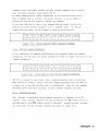
CONTENTS
Section 1.
General Description
1.1
Introduction.. . . . . . . . . . . . . . . . . . . . • . . . . . . . . . . . . . . . . . . . . . . . . . . . . . . . . . . .
1
1.2
Notes on Usage . . • . . . . . . . . . . . . . . . . . . • . . . . . . . . . . . . . . . . . . . . . . . . . . . . . . . . .
1
1.3
Features.............................................................
2
1.4
Corrunand Description List . . . . . . . . . . . . . . . . . • . . . . . . . . . . . . . . . . . . . . . . . . . . .
3
Section 2.
Pin Description
2.1
Pin Configuration . . . . . . . . . . . . . . . . . . . . . . . . . • . . . . . . . . . . . • • . . . . . . . . . . . . .
5
2.2
Signal Description . . . . • . . . . . . . . . • . . . . . . . . . . . . . . . . . . . . . . . . . . . . . . . . . . . .
8
Section 3.
Internal Registers
3.1
Internal Register Access . . . . . . . . • . . . . . . . . . . . . . . . . . . . . . . . . . . . . . . . . . . . . 12
3.2
Internal Register Functions . . . . . . . . . . . . . . • . . • . . . . . . . . . . . . . . . . . . . . . . . . 12
Section 4.
Host Interface
4.1
68 Series Interface (IFS
1)
. . . . . . • . . . . . . • . . . • . . . . . . . . . . . . . . . . • . . . . 14
4.2
80 Series Interface (IFS
0)
. . . . . • . . . . . . • . . . . . . . . . . • . . . . . . . . . . . . . . • 14
Section 5.
Drive Polling
. . . . . . . . . . . . . . . . . . . . • . . . . . . . . . . . . . . • . . . . . . . . . . . . 16
Section 6.
Corrunand Description
6.1
Corrunand Code List
6.2
Corrunand Parameters
6.3
Result Parameters
6.4
Issuing Corrunands
6.5
Corrunand Functions
6.6
Track Format
6.7
Corrunand Code Rejection
Section 7.
. . . . . . . . . . . . . . . . . . . . . . . . . . • . . . . . . • . . . . . . . . . . . . . . . .. 18
. . . . . . . . . . . . . . . . . . . . . . . . . . . . . . . . • . . . . . . . . . . . • • . . .. 19
. . . . . . . . . . . . . . . . . . . . . . . . . . . . . . . . . . . • • . . . . . . . . . . . . . . 28
. . . . . . . • . . . . . . . . . . . . . . . . . . . • . . . . . . . . • . . . . . . . . . . . . . . . 32
. . . . . . . . • . . . . . . . . . . . . . . . . . . . . • . . . . . . . . . . . • . . • . . . . .. 43
• • . • • • • • • • • • • • . • • • • • . . • • • • • • • • • • • • • • • . • • • • . • • • • • • • • • • • .• 74
.••••.••••..••••..••.•••••.••.•••••••..••••..•
75
VFO Circuit
7.1
VFO Synchronization
. . . . . . . . . . . . . . . . . . . . . • . . . . . . . . . . . • . . . . . . . . . . . . . . . 85
7.2
Controlling the VFO
. . . . . . . . • . • . . . . . . . . . . . . . . . . . . . . . • . . . . . . . . . . • . . . . . 85
7.3
PLL Circuit
. . . . . . . . . . . . . . . . . . . . . . . . . . . . . . . . . . . . . • . . • . . . . . . . . . . . . . . . 88
Section 8.
Write Precompensation Circuit
Section 9.
System Application
9.1
System Configuration
.......................•....•.•..•......•.•..... 90
9.2
System Operation Sequence
9.3
Data Transfer Timing
9.4
Data Transfer Completion Timing
9.5
FDC Control
9.6
Host Interface
9.7
FDD Interface
Section 10.
.....•.........•....•...•....... 89
.. . . . • . . . . . . . . . . • . . . . . • . . . . . . . • . . . . . . • . . . .. 91
... • . . . . . • . . . . . . . . . . . . . . . . . . . . . . . . . . . . . . . . • . . . .. 92
.....•••.........•..............•..•. 93
....•.......•.....•.....•..•........•..............•..... 97
. . . . . . . . . . • • . . • . . . . . . . . . . . . . . • . . . . . . . . . . . • . . . . . . . . . . .. 97
.................•..............•....................•. 106
Characteristics
10.1
Absolute Maximum Ratings
10.2
Recommended Operating Conditions
10.3
Electrical Characteristics
10.4
Package Dimensions ................................................•. 124
....•....................•................. 114
........•..•.....•........•••...... 114
.•....•...••....•........................ 115
SECTION 1.
1.1
GENERAL DESCRIPTION
INTRODUCTION
Recently, floppy disc drives (FDDs) have taken on the following features:
Smaller size
• Larger capacity
· Higher speed
· Lower power dissipation
· Lower cost
To control and manage data transfers to and from such FDDs, Hitachi has
developed a new Floppy Disk Controller (FDe).
This FDC has the following major
features.
1.
Built-in VFO and write precompensation circuits:
Since this FDC contains
a built-in VFO circuit and a write precompensation circuit, which
previously had to be externally installed, a compact system and lower system
construction cost can be achieved.
The VFO circuit is an analog PLL
type to meet the high accuracy requirements for controlling large-capacity,
high-speed FDDs.
2.
CMOS process plus SLEEP command:
ing CMOS process.
Low power dissipation is achieved utiliz-
Furthermore, a SLEEP command which enables the FDC to
enter a very low power dissipation mode is provided for use in FDD systems
requiring or having a standby mode.
3.
Command code compatible with standard FDCs:
This FDC is command code
compatible with standard FDCs, making it easy to be integrated into an
existing design.
Furthermore, for easy use in existing systems, the FDC
has various modes to include control of all types of FDDs, and interfaces
for both 68- and 80- series microprocessors.
1.2
NOTES ON USAGE
· Stepping rate is programmable from 1 ms to 16 ms by 1 ms increments in
both 5" and 8" modes.
In 5" mode, the stepping rate is also programmable
from 2 ms to 32 ms by 2 ms increments.
· There is no read skip area around the Index.
· Requires no write clock.
• Stepping rate is always exact as specified.
HITACHI
• The delay from the detection of USO, USl signals to read the FDD status
is 3 lls.
The delay is 2 ms (8" mode) or 4 ms (5" mode) from WGATE signal's falling
edge to HSEL signal's rising edge in multitrack write mode.
• Recalibrateoperation is based on 255 step pulses.
WDATA signal is always at low level when WGATE signal is at low level.
• IRQ and DREQ become inactive (high level) automatically when a data overrun
error is detected.
1.3
FEATURES
• On-chip high accuracy data separator (adjustment-free analog VFO system)
- No adjustment required
• On-chip write precompensation circuit
Delay times programmable from 0 to 750 ns in 62.5 ns increments
Different delay times for inner and outer tracks
- Outer to inner switchover track programmable from 1 to 254
· Low power dissipation
- CMOS circuit plus SLEEP command
· Command code compatible with standard FDCs
· Selectable recording codes
- FM and MFM
· Serial data transfer rate
- FM mode: 125, 150, 250 Kbps
- MFM mode: 250, 300, 500 Kbps
· Selectable DMA and Non-DMA host data transfers
• Compatible with both 68- and 80- series microprocessors
• Formatting
- Both IBM and ECMA (ISO) track formats supported
· Error checking
- 16-bit CRC generator and checker incorporated
.
16 12 5
CRe polynomlal: x +x +x +1
• Multi-sector and multi-track read/write capability
• Data scan capability
- Scans a single sector or an entire cylinder comparing the disk data
byte-by-byte with the host memory data
· Multi-drive parallel seek capability
· Stepping rate, head load time, and head unload time programmable
- Stepping rate programmable in 1 ms increments in 5" mode
2
HITACHI
. Maximum drive control range:
- Number of drives:
4
- Number of cylinders:
- Number of sectors:
- Number of heads:
255 cylinders/drive
255 sectors/track
2 heads/drive
. Sector length programmable
- 128, 256, 512, 1024, 2048, 4096, 8192 bytes/sector
1.4
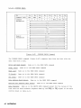
COMMAND DESCRIPTION LIST
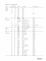
This FDC supports 20 commands listed in Table 1-1.
READ LONG and WRITE LONG
commands become valid only after command SPECIFY 2 has been issued.
Table 1-1.
FDC Commands
Commands
Functions
READ DATA
Reads data from any specified sector(s) except the
deleted sector(s)
READ DELETED DATA
Reads data from any specified sector(s) containing
a data address mark of F8
READ ERRONEOUS DATA
Reads data from the first sector immediately after the
index to the end of track regardless whether there
are errors or not
READ ID
Reads the first errorfree ID encountered on a track
WRITE DATA
Writes data to any specified sector(s) using a data
address mark of FB
WRITE DELETED DATA
Writes data to any specified sector(s) using a data
address mark of F8
WRITE FORMAT
Formats the track where the head is currently
positioned
SEEK
Moves the selected FDD's head to a specified track
RECALIBRATE
Moves the selected FDD's head to track 0
COMPARE EQUAL
COMPARE LOW OR EQUAL
Compares the data read from the selected FDD with the
data sent from the host according to the chosen
command
COMPARE HIGH OR EQUAL
CHECK DEVICE STATUS
Reads the selected FDD's status
CHECK INTERRUPT STATUS
Reads the interrupt causes
HITACHI
3
Table 1-1.
FDC Commands (cont)
Commands
Functions
SPECIFY 1
Specifies the FDC operating mode and sets up the
various timers in the FDC
SPECIFY 2*
SLEEP
*
Sets the FDC to the low power dissipation mode
ABORT
*
Software reset command
READ LONG
WRITE LONG
*
Reads the CRC bytes as well as the data from a sector
to the host
*
writes the CRC bytes as well as the data to a sector
from the host
Note: Commands marked with
this FDC.
commands.
4
HITACHI
*
are newly added commands which are unique to
Rest of the commands are identical to other standard FDC
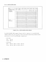
SECTION 2.
2.1
PIN DESCRIPTION
PIN CONFIGURATION
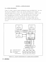
Figure 2-1 shows the pin configuration.
Table 2-1 describes the pin functions.
lCT
VCC1
NUM1
NUM2
SFORM
HDIR
STEP
IFS
8"/5"
41
E,RD
R/W,WR
CS
10
DACK
11
RS
VSS1
12
FAULT
TRKO
INDEX
13
usa
Do
14
D1
15
DSIDE
16
17
18
19
20
US1
EARLY
LATE
WDATA
WGATE
RDATA
VCC2
23
NC
NC
VSS2
24
ClK
21
22
Figure 2-1.
Pin Configuration
HITACHI
5
VCC1-VCC4
VSS1 -VSS3
NUM1
NUM2
SFORM
IFS
8"/~
RESET
E,RD
R/W,WR
CS
DACK
RS
Do
01
02
03
04
05
06
07
lCT
FRES
HlOAO
HSEl
HDIR
STEP
READY
WPRT
DSIDE
FAULT
TRKO
INDEX
USO
US1
EARLY
LATE
WOATA
WGATE
RDATA
NC
ClK
+5V
Ground
Not User Mode 1
Not User Mode 2
Select Format
Interface Select
8" /5" Mode Select
Reset
Enable, Read
Read/Write, Write
Chip Select
DMA Acknowledge
Register Select
Data Bus 0-7
DREQ
IRQ
OENO
low Current
Fault Reset
Head load
Head Select
Head Direction
Step
Ready
Write Protected
Double Sided
Fault
Track 00
Index
Unit Select 0
Unit Select 1
Early
late
Write Data
Write Gate
Read Data
No Connection
Clock
DMA Request
Interrupt Request
DMA End
NC
NC
51
NC
NC
READY
E,RD
R/W,WR
DSIDE
FAULT
TRKO
INDEX
NC
NC
NC
CS
RS
NC
NC
VSS1
USD
USl
Vsss
Do
D\
EARLY
LATE
WDATA
WGATE
D2
Ds
D4
NC
NC
33
19
Top
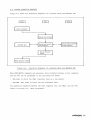
Figure 2-2.
6
HITACHI
View
Pin Arrangement (FP-64)
NC
Table 2-1.
Type
Pin Functions
Pin No.
DP-48 FP-64
Symbol
Pin Name
Power
1
58
VCCI
VCCI
Supply,
13
11
VSSI
VSSI
Clock
29
31
VCC2
VCC2
26
28
VSS2
VSS2
25
27
CLK
Clock
59
VCC3
VCC3
26
VCC4
VCC4
12
VSS3
VSS3
7
3
RESET
Reset
MPU
Interface
Input/Output
Input
Input
8
4
E, RD
Enable, Read
Input
9
5
R/W, WR
Read/write, Write
Input
10
6
CS
Chip select
Input
12
8
RS
Register select
Input
14-21
13-22 DO-D7
Data bus, bits 0-7
Input/Output
23
24
IRQ
Interrupt request
Output
DMA
11
7
DACK
DMA acknowledge
Input
Control
22
23
DREQ
DMA request
Output
24
25
DEND
DMA end
Input
FDD
30
32
RDATA
Read data
Input
Interface
31
35
WGATE
write gate
Output
32
36
WDATA
Write data
Output
33
37
LATE
Late
Output
34
38
EARLY
Early
Output
35
39
USI
Unit select 1
Output
36
40
USO
unit select 0
Output
37
44
INDEX
Index
Input
38
45
TRKO
Track 0
Input
39
46
FAULT
Fault
Input
40
47
DSIDE
Double sided
Input
41
48
WPRT
Write protect
Input
42
49
READY
Ready
Input
43
52
STEP
Step
Output
44
53
HDIR
Head direction
Output
45
54
HSEL
Head select
Output
46
55
HLOAD
Head load
Output
47
56
FRES
Fault reset
Output
48
57
LCT
Low current
Output
HITACHI
7
Table 2-1.
Pin Functions (cont)
Type
Pin No.
DP-48 FP-64
FDC
Symbol
Pin Name
Input/Output
SFORM
Select format
Input
4
62
Function
5
63
IFS
Interface select
Input
Switching
6
64
8"/5"
8"/5" mode select
Input
Others
2
60
NUMI
Not-user mode 1
Input
3
61
NUM2
Not-user mode 2
Input
27
28
1,2
9,10
18,19
29,30
33,34
41-43
50,51
NC
No Connection
2.2
SIGNAL DESCRIPTION
2.2.1
Power Supply, Clock
VCC1, VCC2, VCC3, VCC4, VSS1, VSS2, VSS3 (power Supply): VCC1, VCC3, VCC4,
VSS 1' and VSS3 are the power and "ground for the logic area (+5 V ±5%).
and VSS3 are connected to ground.
the internal VFO (+5 V ±5%).
VSS1
VCC2 and VSS2 are the power and ground for
VSS 2 is connected to ground.
CLK (Clock): CLK is the 16 MHz clock input (19.2 MHz for 150 and 300 kbps).
2.2.2
MPU Interface
RESET (Reset): RESET sets the DREQ and IRQ signals high and sets all the other
output signals low.
It forces DO-D7 into the input state.
E, Ri5 (Enable, Read), R/W,
E, RD and R/W, WR depend
Table 2-2.
E,
and R/W,
(Read/Write, Write): The functions of
on the IFS input (table 2-2).
WR
Function
Signal
IFS
E, RD
0
RD
Accepts the 80-series Read signal
1
E
Accepts the 68-series Enable signal
0
WR
Accepts the 80-series Write signal
R!W
Accepts the 68-series Read/Write signal
R/W, WR
1
CS
Function
(Chip Select): CS selects the chip and enables the read/write of the internal
registers.
8
R5
WR
HITACHI
RS (Register Select): RS selects the internal register on which an MPU
read/write is performed (table 2-3).
Table 2-3.
RS Function
RS
Register Selected
Conditions
o
Status Register
Read
Abort Register
Write
Data Register
Read/Write
1
DO-D7
(Data Bus): DO-D7 form the bidirectional 8-bit data bus, enabled by
read/write.
IRQ (Interrupt Request): IRQ requests data transfer with the MPU in Non-DMA
mode.
It informs the MPU that a READ, WRITE, or SEEK command has been completed.
When IFS is high, IRQ becomes an open drain output.
2.2.3
DMA Control
BACK (DMA Acknowledge): DACK receives the DMA acknowledge signal from the DMAC
during a DMA transfer.
5RE'Q
(DMA Request): DREQ requests the DMAC to perform a DMA transfer.
BEND
(DMA End): DEND receives the DMA end signal from the DMAC and terminates the
DMA transfer.
2.2.4
FDD Interface
RDATA (Read Data): RDATA inputs the read data signal from the FDD.
WGATE (Write Gate): WGATE outputs the write control signal to the FDD.
WDATA (Write Data): WDATA outputs the write data signal to the FDD.
LATE, EARLY (Late, Early): The LATE and EARLY output the write precompensation
control signals used to advance or delay the write data before sending it to the FDD.
U8l, USO (Unit Select 1, 0): The USl and
usa
unit select outputs select the FDD.
A maximum of 4 FDDs can be selected by decoding USl and USO (table 2-4).
Table 2-4
FDD Selection
USl
USO
o
o
FDD 0
o
1
FDD 1
FDD
1
o
FDD 2
1
1
FDD 3
HITACHI
9
INDEX (Index): INDEX inputs the index signal from the FDD.
TRKO (Track 0): TRKO inputs the track 00 signal from the FDD.
FAULT (Fauit): FAULT inputs the fault signal from the FDD.
DSIDE (Double Sided): DSIDE inputs the double sided signal from the FDD.
WPRT (Write Protect): WPRT inputs the write protected signal from the FDD.
READY (Ready): READY inputs the ready signal from the FDD.
STEP (Step): The STEP output moves the FDD head.
HDIR (Head Direction): The HDIR output controls the direction of FDD head
movement. HDIR = 0 indic'ates outward direction (towards track 0), while HDIR
1
indicates inward direction.
HSEL (Head Select): The HSEL output selects the FDD head.
HSEL
=
0 selects head 0, while HSEL
=
1 selects head 1.
HLOAD (Head Load): The HLOAD output directs the FDD to load the heads onto the disk.
FRES (Fault Reset): The FRES output resets the FDD fault status FF.
LCT (Low Current): The LCT output reduces the FDD write current for inner
tracks.
After the SPECIFY 1 command is issued, the most outer position of the
low current tracks is specified as track 43.
For tracks
~
this track, LCT
= 1.
A different most outer track position can be specified by the SPECIFY 2 command.
2.2.5
FDC Function Switching
SFORM (Select Format): The SFORM input selects the track format for formatting.
SFORM high selects IBM format, SFORM low selects ECMA (ISO) format.
needed for formatting only.
SFORM is
The FDC can read or write in either format
regardless of the SFORM input level.
IFS (Interface Select): The IFS input specifies the host interface.
IFS defines
the functions of pins 8 and 9 (E, RD and R/W, WR) as shown in table 2-2.
IFS
0 for 80-series interface, IFS = 1 for 68-series interface.
8"/'.5'i (8"/5" Mode Select): The 8"/5" input selects the FDD type.
It specifies
the drive data rate depending on the modulation method selected (table 2-5).
Table 2-5.
Drive Data Rate
8"/5"
FM
0
125 kbits/s
150 kbits/s
1
250 kbits/s
Note: When CLK
2.2.6
MFM
250 kbits/s
(Note)
300 kbits/s
(Note)
500 kbits/s
19.2 MHz
Others
NUMl, NUM2 (Not-User Mode 1, 2): NUMI and NUM2 are not for user applications.
10 HITACHI
They must be tied to low.
NC (No Connection): NC pins require no connection.
HITACHI 11
SECTION 3.
3.1
INTERNAL REGISTERS
INTERNAL REGISTER ACCESS
The host can access three registers: Data register (DTR), status register (STR) ,
and abort register (ATR).
These registers are selected by the RS signal and
read/write operations (table 3-1).
Table 3-1.
Register Selection
RS
Read/Write
Selected Register
o
Read
Status Register (STR)
Write
Abort Register (ATR)
Read/Write
Data Register (DTR)
1
3.2
INTERNAL REGISTER FUNCTIONS
3.2.1
Status Register
The status register (figure 3-1) is a read-only register
whi~h
indicates the
FDC status and also whether each FDD selected by signals USO and USl is currently
performing a seek or recalibrate operation.
STR
Bit
7
Symbols
6
5
Figure 3-1.
Bit 7
4
3
Z
I
0
TXR DIR NDM BSY D3S DZS DIS DOS
Status Register
TXR (Transfer Ready): Bit 7 is set to 1 when DTR is in the read/write
enabled state and it is cleared to 0 when data starts to be read or written
by the host.
Bit 6
DIR (Data Direction): Bit 6 indicates the data transfer direction
between the host and the FDC.
DIR
0: The host writes data to the FDC.
DIR
1: The host reads data from the FDC.
Bit 5
NDM (Non-DMA Mode): Bit 5 set to 1 indicates that the FDC transfers data
in Non-DMA mode.
When Non-DMA mode is selected by commands SPECIFY 1 and
SPECIFY 2, this bit is cleared to 0, except during the execution of read/write
related commands.
12 HITACHI
Bit 4
BSY (Controller Busy): Bit 4 is set to 1 when the FDC cannot accept the
next command because it is decoding or executing a command.
except for the ABORT command, must be issued only when BSY
Bit 0-3
A new command,
= O.
DOS-D3S (Drives 0-3 Seek): Bits 0-3 are set to 1 when the FDD selected
by signals
usa
and USI is executing a SEEK or RECALIBRATE command.
corresponds to FDDO and bit 3 to FDD3.
Bit 0
Bits DOS to D3S are lIs when
the seek or recalibrate command is issued.
Even if all of the step pulses
are output, these bits stay as lIs until the SEEK and RECALIBRATE end status
information is accepted by the CHECK INTERRUPT STATUS command.
3.2.2
Abort Register
Abort register is a write-only register used exclusively for the ABORT command.
ABORT command is issued by writing HEX FF into this register.
This command is
valid when the RESET signal is inactive regardless of the state of the FDC.
Values other than HEX FF written into this register are ignored by the FDC.
3.2.3
Data Register
Data register is a read/write register (actually a stack of registers with
only one connected to the data bus at a time) which is used to receive commands
and command parameters, transfer data, and read out result parameters.
HITACHI 13
SECTION 4.
HOST INTERFACE
This FDC can easily be interfaced to the 68- as well as the 80-series 8-bit
devices.
4.1
IFS (pin 5) is used for selecting between 68-and 80-series interfaces.
68 SERIES INTERFACE (IFS
QFP
DIP
Pin 4
Pin 8:
E
Pin 5
Pin 9:
R/W
Pin 24 Pin 23 (IRQ):
1)
Open-drain output
For the 68-series interface only, the data flow direction controlled by R/W
input (pin 9) is reversed between DMA and Non-DMA transfers (table 4..,..1).
Here, DMA FDC
access is by DACK signal (pin 11), and Non-DMA FDC access is
by CS signal (pin 10).
Table 4-1.
Data Transfer 68-Series
R/W
E
Data Transfer Direction
1
0
1
FDC
~
Main memory
0
1
1
1
Main memory
~
FDC
Non-
1
0
0
1
Host
~
FDC
DMA
1
0
1
1
FDC
~
Host
Mode
DACK
DMA
0
CS
When the FDC is accessed by the DACK signal, the RS. signal (pin 12) is ignored,
andDTR (data register) is always accessed.
4.2
80 SERIES INTERFACE (IFS
QFP
DIP
Pin 4
Pin 8
RD
Pin 5
Pin 9
WR
Pin 24 Pin 23 IRQ:
0)
CMOS output the same as the other output pins
Table 4-2 shows the data transfer signals.
Table 4-2.
Mode
DACK
DMA
Data Transfer, 80-Series
CS
RD
WR
0
1
1
0
Main memory
~
FDC
0
1
0
1
FDC
~
Main memory
Non-
1
0
1
0
Host
~
FDC
DMA
1
0
0
1
FDC
14 HITACHI
Data Transfer Direction
II
Host
During DMA transfer, in which the FDC is accessed by the DAC:K signal, the RS
signal (pin 12) is ignored and DTR (data register) is always acCessed.
HITACHI
15
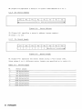
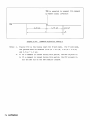
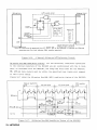
SECTION 5.
DRIVE POLLING
This FOC performs drive polling every 1 ms (actually 1. 024 ms) in 8" mode
and every 2 ms (2.048 ms) in 5" mode during command waiting.
and head loading, no polling is performed.
During sleep
Polling and seek operation
(step pulse output) are performed concurrently.
I
·--------1024 l1sec, 2048 l1sec
(8" mode), (5" mode)
1-01
usa
USl
-_-+-I--11-011- 128 l1sec, 256 l1sec
I
I
(8" mode), (5" mode)
CLK
Figure 5-1.
16 MHz
Drive Selection Timing during Polling
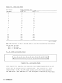
USO and USl signals are changed (Figure 5-1) and the Ready signals of all
four drives are polled (Figure 5-2).
During this time, a step pulse is
issued to the drive requiring it (Figure 5-2).
When high speed seek mode is
specified using SPECIFY 2 command, 1 ms polling is performed even in 5" mode.
us 0,1
STEP
--~~~------------------------i------------ln'----
t
I
Ready signal is
Polled
1
.. I ..
I •
I
Figure 5-2.
16 HITACHI
16.usee, 32.usee
CS"mode), C5"mode)
16 .usee, 32 .usee
CS"mode), C5"mode)
CLK
Ready Signal Polling and Step Pulse Output Timing
16 MHz
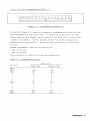
During polling, if the ready signal level is inverted compared to the last
time it was polled:
INC (interrupt code) bits of SSBO are set to CDS (Change in Drive Status)
code,
. USI and USO bits of SSBO are updated to the drive number whose ready signal
is inverted, and
IRQ signal is set active to request the host to issue CHECK INTERRUPT STATUS
cormnand.
Also, when a drive completes a seek operation, IRQ is set active to make a
request for CHECK INTERRUPT STATUS command.
When a CHECK INTERRUPT STATUS cormnand request source is accepted from
the FDC by the CHECK INTERRUPT STATUS command, if there is no Seek-End
status information in .the FDC, the next cormnand request is not generated
even if the Ready Signal Inversion status information is present.
However, when the CHECK INTERRUPT STATUS cormnand is issued, the command is
not treated as the INVALID command; the Ready Signal Inversion status
information can be accepted.
When Ready Signal Inversion is detected while
the IRQ signal is inactive, the CHECK INTERRUPT STATUS cormnand is requested
by activating the IRQ signal.
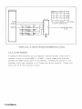
FDDO
FDC
internal
status
FDDI
READY inversion! SEEK end
FDD2
FDD3
1-
1-
READY inversion
-
!
READY inversion
!
-
IRQ does
IR.;.;.Q_ _ _.....
r
CIS
I
FDDO
status
return
1j 1 I
CIS
FDDI CIS
status
return
FDD2
status
return
r
CIS
I
FDD3
status
return
CIS: CHECK INTERRUPT STATUS cormnand
If the FDC has statuses for more than one CIS command request, it returns
FDD statuses to the host each time a CIS cormnand is issued, starting at the
lowest-numbered FDD's status.
HITACHI
17
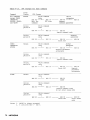
SECTION 6.
COMMAND DESCRIPTION
COMMAND CODE LIST
6.1
Table 6-1 lists the FDC commands and the corresponding command codes.
Table 6-l.
Command Codes
Command Codes
Commands
D7
D6
DS
D4
D3
D2
D1
DO
READ DATA
MT
MM
SD
0
0
1
1
0
READ DELETED DA'l'A
MT
MM
SD
0
1
1
0
0
READ ERRONEOUS DATA
0
MM
0
0
0
0
1
0
READ ID
0
MM
0
0
1
0
1
0
WRITE DATA
MT
MM
0
0
0
1
0
1
WRITE DELETED DATA
MT
MM
0
0
1
0
0
1
WRITE FORMAT
0
MM
0
0
1
1
0
1
SEEK
0
0
0
0
1
1
1
1
RECALIBRATE
0
0
0
0
0
1
1
1
COMPARE EQUAL
MT
MM
SD
1
0
0
0
1
COMPARE LOW OR EQUAL
MT
MM
SD
1
1
0
0
1
COMPARE HIGH OR EQUAL
MT
MM
SD
1
1
1
0
1
CHECK DEVICE STATUS
0
0
0
0
0
1
0
0
CHECK INTERRUPT STATUS
0
0
0
0
1
0
0
0
SPECIFY 1
0
0
0
0
0
0
1
1
SPECIFY 2
0
A
H
0
1
0
1
1
SLEEP
0
0
0
0
1
1
1
0
ABORT
1
1
1
1
1
1
1
1
READ LONG
MT
MM
SD
1
0
0
1
0
WRITE LONG
MT
MM
0
1
0
1
1
0
MT: Multi Track
MT = 1 specifies read/write of multi tracks.
MM: MFM Mode
MM= 0 selects FM mode
MM= 1 selects MFM mode
SD: Skip DDAM
Sector with DDAM (deleted data address mark) is read or skipped depending
on whether SD
18 HITACHI
=
0 or 1.
When SD
=
1, the sector with DDAM is skipped.
A:
Auto precompensation
When A
H:
=
1, auto write precompensation is performed.
High speed seek
H
6.2
=
1 selects high speed seek mode.
COMMAND PARAMETERS
6.2.1
HSL-US: Head Select-Unit Select
Do
x
x
x
x
x
Don't
care
HSL
Head
Select
US
1
Unit
Select 1
usa
Unit
SelectO
Figure 6-1.
usa
x
HSL
US 1
USa
Head Select-Unit Select
and USl bits (figure 6-1) specify the FDD that performs the command.
HSL specifies the read/write head to be used.
When SEEK and RECALIBRATE
commands are issued, HSL has no meaning.
6.2.2
CA: Cylinder Address
Figure 6-2.
Cylinder Address
CA (figure 6-2) specifies a sector's or track's cylinder address.
CA range:
6.2.3
a
to 255
HA: Head Address
Do
o
o
o
o
Figure 6-3.
o
o
o
HA
Head Address
HITACHI
19
HA (figure 6-3) specifies a sector's or track's head address as 0 or 1.
6.2.4
SA: Sector Address
Figure 6-4.
Sector Address
SA (Figure 6-4) specifies a sector's address (sector number).
SA range: 1 to 255
6.2.5
RL: Record Length
D7
D6
D5
D4
D3
0
0
0
0
0
Figure 6-5.
D2
I
-Record
Dl
I
Do
Len gth---.
Record Length
RL (figure 6-5) specifies the sector length using a 3-bit binary code.
Using values 0 to 6, different sector lengths are specified as in table 6-2.
Table 6-2.
RL
Record Length
Sector Length
0
128 Bytes/sector
1
256 Bytes/sector
2
512 Bytes/sector
3
1024 Bytes/sector
4
2048 Bytes/sector
5
4096 Bytes/sector
6
8192 Bytes/sector
20 HITACHI
6.2.6
ESN:
End Sector Number
Figure 6-6.
End Sector Number
ESN (figure 6-6) specifies the sector number of the last sector on the track.
This number need not be the same as the actual (physical) last sector number.
Read/Write access starts from the sector specified by SA, cQntinues to and
ends with the sector specified by ESN on the same track.
However, if DEND
signal is received during this time, the access terminates immediately.
ESN range: 1 to 255.
6.2.7
However, for COMPARE commands, the range is 1 to 253.
GSL: Gap Skip Length
Gap Skip Length
Figure 6-7.
Gap Skip Length
GSL (figure 6-7) specifies the number of bytes skipped in between sectors as GAP3.
6.2.8
MNL: Meaning Length
~---------------------- Meaning
Figure 6-8.
Length
Meaning Length
To access part of a sector, MNL (Figure 6-8) specifies the byte count of data
to be accessed.
This function is valid only for sectors with RL
=
0 (128 bytes/
sector) .
Values from 0 to 255 can be set for MNL. If a value exceeding 128 (HEX 80) is
specified, it is treated as 128, and the entire sector is accessed.
sectors with RL
~
When
0 are accessed, MNL has no effect.
HITACHI 21
6.2.9
SCNT: Sector Count
D
D
",,1.
___D_7_ _ __6_ _ __5_ _
s:c
40r C
t
Figure 6-9.
o:~
D_°-t.~1
t ___D_2_ _ _D_l_ _ _
Sector Count
SCNT (figure 6-9) specifies the sector count for formatting a track.
SCNT range: 1 to 255
6.2.10
GP3L: Gap 3 Length
I. .__-D-7----D-6---D-5--G~p4
3
Figure 6-10.
Le~;th
_ _D_2_ _ _ _D_I_ _ _
D_o~.1
Gap 3 Length
GP3L (figure 6-10) specifies in bytes the GAP3 length used in formatting a
track.
GP3L range: 1 to 255
6.2.11
DUD: Dummy Data
I·
D7
D6
D5
D4
D3
D2
Dummy Data
Figure 6-1l.
Dl
Do
·1
Dummy Data
DUD (figure 6-11) specifies the dummy data pattern to be written into a sector's
data area when formatting.
DUD range: 0 to 255
22 HITACHI
6.2.12
STEP: Step
Do
o
o
o
o
o
Figure 6-12.
o
S T EP
Step
STEP (figure 6-12) specifies the sector increment for incrementing the sectors
whose data is to be compared byte-by-byte with the data sent from the host using
a COMPARE command.
STEP
1: Data from contiguous sectors is used for comparison.
STEP
2: Data from alternate sectors is used for comparison.
6.2.13
NCN: New Cylinder Number
D7
D6
I
I
D5
I
D4
I
New CyI inder
Figure 6-13.
D3
I
D2
I
Dl
I
Do
..
Number
New Cylinder Number
NCN (figure 6-13) specifies the cylinder number to which the head is to be moved.
NCN range: 0 to 255.
6.2.14
STR-HDUT: Stepping Rate-Head Unload Time
D7
I
D6
I
Stepping
D5
Rate
Figure 6-14.
I
D4
D3
I
D2
I
Dl
I
Head Unload Time
Do
.---..
Stepping Rate-Head Unload Time
STR-HDUT (figure 6-14) is a one-byte code in which the upper 4 bits represent
STR (stepping rate) and the lower 4 bits represent HDUT (head unload time).
STR: STR specifies the step pulse interval (stepping rate) for the seek and
recalibrate operations. Using values 1 to 15, different stepping rates are
HITACHI 23
specified as in table 6-3.
Table 6-3.
Values
(Decimal)
Stepping Rates
Stepping Rate (ms)
8"/5" = 1 or high-speed
8"/5" = 0 and high-speed
seek mode is selected
seek mode is not selected
o
16
32
1
15
30
2
14
28
3
13
26
4
12
24
5
11
22
6
10
20
7
9
18
8
8
16
9
7
14
10
6
12
11
5
10
12
4
8
13
3
6
14
2
4
15
1
2
eLK = 16 MHz
24 HITACHI
HOUT: HDUT specifies the time to wait from the completion of the head-load
associated command execution before deactivating the head load signal.
Using values 0 to 15, different head unload times are specified as in table 6-4.
Table 6-4.
Head Unload Times
Set Values
Head Unload Time (ms)
(Decimal)
8" /5"
=
8"/5"
1
0
0
0
1
16
32
2
32
64
3
48
96
4
64
128
5
80
160
6
96
192
7
112
224
8
128
256
9
144
288
10
160
320
11
176
352
12
192
384
13
208
416
14
224
448
15
240
480
0
eLK
6.2.15
16 MHz
HDLT-NDM: Head Load Time-Non-DMA Mode
Do
NDM
Figure 6-15.
Head Load Time-Non-DMA Mode
The upper 7 bits of HDLT-NDM (figure 6-15) denote HDLT (head load time) while
the lowest bit denotes NDM (Non-DMA mode).
HDLT: HOLT specifies the time to walt from setting the head load signal active
to start the command execution.
When specifying HDLT, an allowance for head
settle waiting time should be made also.
Using values 0 to 127, different
head load times are specified as in table 6-5.
HITACHI 25
Head Load Times
Table 6-5.
Set Values
Head Load Time (ms)
(Decimal)
8"/5"
=
8"/5"
1
0
0
0
1
2
4
2
4
8
3
6
12
4
8
16
5
10
20
6
12
24
7
14
28
8
16
32
+
+
+
124
248
496
125
250
500
126
252
504
127
254
508
0
CLK
~:
=
16 MHz
NDM specifies if DMA or Non-DMA mode is used for transferring data between
the FDC and the host.
NDM
0: DMA mode
NDM
1: Non-DMA mode
6.2.16
LCTK: Low Current Track
~u
D
..-_D_7_ _ __6_ _ _D_5_ Low D
"",1.
Figure 6-16.
D
r r en t
~
.~1
r ack _D_2_ _ _D_l_ _ _D_O__
Low Current Track
LCTK (figure 6-16) specifies the cross-over track number beyond which the LCT
signal (pin 48) becomes active in SPECIFY2 mode.
With LCTK set to a value
ranging from 1 to 255, the LCT signal becomes active for tracks exceeding
the LCTK value.
26 HITACHI
Witp LCTK set to 0, the LCT signal is inactive at every track.
6.2.17
PCl, PCO: Precompensation Delay 1, 0
D7
D6
5
4
t - __ _ _ _ __ P C 1_D__ _ _D__ .+1..._
Figure 6-17.
D2
D3
_ _ _ _ __ P C 0 _D_l_ _ _D_0--l
Precompensation Delay 1, 0
PCl and PCO (figure 6-17) specify the amount of precompensation delays for the
auto precompensation mode (table 6-6).
PCO specifies the delay for the outer
tracks (smaller track numbers) and PCl specifies the delay for the inner tracks
(larger track numbers).
The FDC switches between PCO and PCl automatically
depending on the head position.
The switch-over track position is specified
by PCDCT.
Maximum programmable values for PCl and PCO are
. HEX C in 5" mode
. HEX 6 in 8" mode
Values exceeding the above limits may cause malfunction.
Table 6-6.
Precompensation Delay
Delay (ns)
PCl, PCO
HEX 0
HEX 1
HEX 2
I
I
I
I
CLK=16 MHz
0
62.5
125
0
52.1
104.2
I
I
I
I
I
I
I
I
I
I
I
I
I
I
I
I
I
HEX 6
I
I
I
I
I
I
HEX B
HEX C
CLK=19.2 MHz
375
I
I
I
I
I
312.5
I
I
I
I
I
I
I
687.5
750
572.9
625
HITACHI 27
6.2.18
PCDCT: Precompensation Delay Change Track
~1
I"."
D
D
4
7
...-D__ _ _
D_6_ _ __5_ _ _ : CDC : 3_ _ __2_ _ _D_l_ _ _D_°-l..
Figure 6-18.
Precompensation Delay Change Track
PCDCT (figure 6-18) specifies the track where the precompensation delay amount
is changed in the auto precompensation mode.
For tracks with a number equal
to or larger than PCDCT, the delay amount is specified by PC1, and for tracks
with a smaller number, the delay is specified by PCO.
PCDCT range: 1 to 255
6.3
RESULT PARAMETERS
6.3.1
CA, HA, SA, and RL: Cylinder Address, Head Address, Sector Address,
Record Length
CA, HA, SA, and RL are provided as command execution results and their values
depend on the command type and how the command execution ended, with or without
errors.
6.3.2
See section 6.5, "Command Functions".
SSBO: Sense Status Byte 0
D7
I
D6
I
N
C
D5
D4
D3
D2
Dl
Do
SED
DER
DN R
HSL
US 1
USO
Figure 6-19.
28 HITACHI
Sense Status Byte 0
INC (Interrupt Code): INC (figure 6-19) indicates the cause of an interrupt
request (table 6-7).
Table 6-7.
Interrupt Code
Code
Symbol
Code Name
Meaning
0
NOR
Normal End
Command normally ended
D7
D6
0
0
1
ABE
Abnormal End
Command abnormally ended
1
0
IVC
Invalid
Command
Issued command is invalid
1
1
CDS
Change in
Drive Status
Ready signal level from a drive is
inverted compared to the last time
it was polled
SED (Seek End): SED is set to 1 at the completion of SEEK and RECALIBRATE
commands.
DER (Drive Error): DER is set to 1 when the fault signal is active during or at
the completion of write related command execution, and when the track 0 signal
cannot be detected from a drive to which 255 step pulses were applied during a
RECALIBRATE command execution.
DNR (Drive Not Ready): DNR is set to 1 when a low level ready signal is
detected from a drive at the start of or during the execution of drive access
commands other than the CHECK DEVICE STATUS command.
HSL (Head Select): HSL indicates the head selected at the completion of command
execution.
In response to the CHECK INTERRUPT STATUS command, a zero is
returned.
USl, USO (Unit Select 1, 0): USI and USO indicate the drive number selected at
the completion of a command execution or the one that caused an interrupt
request.
6.3.3
SSBl: Sense Status Byte 1
D7
D6
D5
D4
D3
D2
Dl
Do
NDE
0
CER
DOR
0
INF
WPM
ANF
Figure 6-20.
Sense Status Byte 1
NDE (No DMA End): NDE (figure 6-20) is set to 1 if the
DEND
signal is not
received active even after the last sector data has been transferred with
a read/write related command.
The last sector is determined depending on
the MT (multi track) bit value as follows:
HITACHI 29
=
. MT
0: The last sector is specified by the ESN (end sector number) byte on
the track of the side specified as part of the command parameters .
=
. MT
1: The last sector is specified by the ESN byte but always corresponds
to the track on side 1.
CER (CRC Error): CER is set to 1 when a CRC error is detected in the ID or
data field.
READ ID command does not have any effect on this bit.
errors in the ID field, only the CER bit is set to 1.
For CRC
For CRC errors in the
data field, the CDF bit of SSB2 as well as the CER bit are set to 1.
DOR (Data Overrun): DOR is set to 1 if the host cannot complete data transfer
requested by the FDC within a specified time to satisfy the FDC data throughput
requirements.
For details, see section 6.5, "Command Functions".
INF
(ID Not Found):
1.
In READ DATA, READ DELETED DATA, READ LONG, WRITE DATA, WRITE DELETED DATA,
The meaning of INF depends on its context.
WRITE LONG, and COMPARE commands: INF is set to 1 if the sector number
(CA, HA, SA, RL) specified by a command parameter or updated during a
multisector read/write operation cannot be found by the time three index
pulses are detected.
2.
In READ ID command: INF is set to 1 when an address mark in the ID field
was detected but a CRC error-free ID was not found by the time three index
pulses were detected.
3.
In READ ERRONEOUS DATA command:
INF is set to 1 if ID data in the FDC does
not match the ID found.
WPM (Write Protected Medium): WPM is set to 1 when an active write protected
signal is detected at 1:he start of write related command execution.
ANF (AM Not Found): ANF is set to 1 if no ID address mark is detected by the
time three index pulses are detected.
ANF as well as the NAM bit of SSB2
are set to 1 when no address mark (data address mark or deleted data
address mark) is detected in the data field within 1 ms after the desired
ID was found, or when the first data other than HEX 00 found after the
desired ID and at least 4 bytes (FM mode) or 5 bytes (MFM mode) of HEX 00
were detected is not AM.
6.3.4
SSB2: Sense Status Byte 2
D7
D6
D5
D4
D3
D2
Dl
Do
0
DDA
CDF
CAD
CCS
CNS
BDC
NAM
Figure 6-21.
30 HITACHI
Sense Status Byte 2
DDA (Deleted Data Address Mark): DDA (figure 6-21) is set to 1 when a deleted
data address mark is
detected.
In executing the READ DELETED DATA command,
however, it is set to 1 when a normal data address mark is detected.
CDF (CRC Error in Data Field): CDF is set to 1 if a CRC error is detected in
the data field.
CAU (Cylinder Address Unmatch):
CAU is set to 1 when the disk ID's CA byte
does not match the command parameter's CA byte, except when the disk ID's
CA byte is HEX FF.
However, CAU is not set by the READ ERRONEOUS DATA command.
CCS (Compare Condition Satisfied): CCS is set to 1 when the equal condition is
satisfied while executing a COMPARE command.
CNS (Compare Condition Not Satisfied): CNS is set to 1 when the specified
compare condition is not satisfied while executing a COMPARE command.
BDC
(Bad Cylinder): BDC is set to 1 when the CA byte read from the disk does
not match the command parameter's CA byte and also when the read CA byte is
HEX FF.
However, BDC is not set by the READ ERRONEOUS DATA command.
NAM (No Data Address Mark): NAM is set to 1 if no address mark (data address
mark or deleted data address mark) is detected in the data field within 1 ms
after the desired ID was found, or when the first data other than HEX 00 found
after the desired ID and at least 4 bytes
(FM mode) or 5 bytes
(MFM mode) of
HEX 00 were detected is not AM.
6.3.5
SSB3: Sense Status Byte 3
D7
D6
D5
D4
D3
D2
Dl
Do
FLT
WPT
RDY
T RZ
DSD
HSL
US 1
USa
FLT; Fault
D S D : Doub I e
WPT: Write Protected
HSL:Head
Select
R D Y : Ready
USl
Unit
Select
TRZ:Track 0
usa
Unit
Select
Figure 6-22.
1)
Sided
0
Sense Status Byte 3
FLT, WPT, RDY, TRZ, and DSD: Sense bits FLT, WPT, RDY, TRZ, and DSD
indicate the status of the drive specified in the CHECK DEVICE STATUS
command.
2)
HSL, US1, and
HSL, US1, and
usa: Sense
usa of the
bits HSL, US1, and
usa
have the same values as
command parameters.
HITACHI 31
6.3.6
PCN: Physical Cylinder Number
.
D7
I
D6
D5
I
D..
I
Physical
Figure 6-23.
I
Da
Cyl inder
D2
I
I
Dl
I
Do
Numbe r
Physical Cylinder Number
PCN (figure 6-23) represents the physical address of the drive head position
stored in the FDC (physical number of the track where a head is currently
placed).
If a SEEK or RECALIBRATE command ends abnormally, the PCN value may
not match the head's current physical address.
When the FOC is reset, the
PCN values for all four drives are set to HEX 00.
Accordingly, drives with
an auto-recalibrate function (a function which automatically moves the heads
onto track 0 at power on)
do not require the RECALIBRATE command to be
issued after the power on reset.
The lower two bits of SSBO read last
indicate which drive the PCN value belongs to.
6.4
ISSUING COMMANDS
6.4.1
Writing Command Codes
Commands can be issued by writing the desired command codes into the FDC.
The
status register must be read before issuing a command.
TXR
DIR
NDM
BSY
D3S
D2S
DIS
DOS
o
o
o
x
x
x
x
Figure 6-24.
Status Register Before Issuing a Commanq
The FDC is ready to accept commands when the status register bits are as shown
in figure 6-24.
When any of the DOS to D3S bits are set to 1:
1.
CHECK DEVICE STATUS command and CHECK INTERRUPT STATUS command can be
issued for all four drives.
However, CHECK INTERRUPT STATUS command is
treated as an invalid command when the FDC has no SEEK end and no READY
inversion status.
2.
SEEK and RECALIBRATE commands can be issued only for drives whose corresponding DOS to D3S bits are zeros.
32 HITACHI
Commands other than CHECK related and SEEK related commands can be issued
when the status register value equals HEX 80.
An ABORT command can be issued independent of the status register value.
When a command code is written, the status register is set as shown in
figure 6-25 and the FDC begins to decode the command.
If the Data Register is read in the command waiting state, the FDC will
malfunction since the FDC considers it as a command issue.
So, during
command waiting state, do not attempt to read the Data Register.
TXR
DIR
NDM
o
o
o
Figure 6-25.
6.4.2
BSY
D3S
DZS
DIS
DOS
x
x
x
x
Status Register After Issuing a Command
Writing Command Parameters
At the completion of command code decoding, for commands requiring command
parameters, the FDC sets the status register as shown in figure 6-26 and wait for
command parameters.
TXR
DIR
NDM
o
o
Figure 6-26.
BSY
D3 S
DZ S
DIS
DOS
x
x
x
x
Status Register Waiting for Command Parameters
TXR bit is cleared to zero every time a command parameter byte is received.
When the FDC is ready to receive the next command parameter byte the TXR bit
is again set to one and the next byte is transferred.
After all the command
parameter bytes have been received, no more transfer requests are made.
6.4.3
Transferring Data
Data transfer is performed during command execution in
request.
r~sponse
to an FDC
Data transfer requests are made by setting the IRQ signal active in
Non-DMA mode or the DREQ signal active in DMA mode.
Status register contents
for both types of data transfer requests are shown in figure 6-27.
HITACHI 33
Read request in Non-DMA mode
TXR
DIR
NDM
BSY
1
D3S
D2 S
DIS
DOS
0
0
0
0
D3S
D2S
DIS
DOS
0
0
0
0
D3S
D2S
DIS
DOS
0
0
0
0
D3S
D2S
DIS
DOS
0
0
0
0
Write request in Non-DMA mode
TXR
DIR
NDM
BSY
0
Read request in DMA mode
TXR
DIR
NDM
BSY
0
Write request in DMA mode
TXR
Figure 6-27.
6.4.4
DIR
NDM
0
0
BSY
Status Register Contents for Various Data Transfer Requests
Transferring Result Status
For commands having a result status, the FDC requests the host to accept the
result parameter bytes at the completion of the command execution. Commands
which have no result status are SEEK, RECALIBRATE, SPECIFY1, SPECIFY2, SLEEP,
and ABORT.
Commands which cause the status register to be set up as shown in
figure 6-28 and request the host to accept the result parameters are: CHECK
DEVICE STATUS, CHECK INTERRUPT STATUS, and INVALID.
TXR
DIR
NDM
o
Figure 6-28.
34 HITACHI
BSY
D3S
D2 S
DIS
DOS
x
x
x
x
Status Register Requesting Result Parameter Transfer (No
IRQ)
The above commands do not activate the IRQ signal in order to transfer the
result parameters.
After one byte of the result parameters has been transferred, TXR and DIR are
cleared to zero.
When the next byte of the result parameters is ready to be
transferred, it is loaded into the data register.
Then both the DIR and TXR
bits of the status register are set to I requesting the host to accept the
new parameter byte.
After the last byte of the result parameters has been
transferred, some dummy data is loaded into the data register, TXR is set to I
and BSY is cleared to 0 to enter the command waiting state (DIR remains zero).
For all the other commands, the result status transfer is performed by setting
the IRQ signal active and the status register as shown in figure 6-29.
The IRQ
signal is active only when the first byte of the result parameters is transferred, and becomes inactive after that.
TXR
DIR
NDM
o
Figure 6-29.
BSY
D3S
D2 S
D1S
DOS
o
o
o
o
Status Register Requesting Result Parameter Transfer (with IRQ)
The first byte of the result parameters is transferred according to the
following sequence of operations.
· IRQ signal is set active
· DIR bit is set to I
Result parameter byte is loaded into the data register
· TXR bit is set to I
· FDC waits for the result parameter byte to be transferred
· Host reads the result parameter byte and TXR bit is reset to
· DIR bit is reset to
o.
o.
· IRQ signal is set inactive.
The remaining bytes are transferred in the same way except that the IRQ signal
is not activated again.
After the last byte of the result parameters is trans-
ferred, some dummy data is loaded into the data register, TXR is set to I and
BSY is cleared to 0 to enter the command waiting state (DIR remains zero).
HITACHI 35
6.4.5
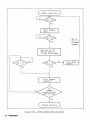
Command Issue Flowchart
Input low level to RESET pin
Issue
SPECIFY
command
Issue
RECALIBRATE
command
Issue
CHECK
INTERRUPT
STATUS
command
Figure 6-30.
36 HITACHI
SPECIFY 1 or SPECIFY 2 command
Move FDD's heads to track 0
Correctly end the RECALIBRATE command
FDC Initial Setup Flowchart
READ, WRITE,
COMPARE command
Read a result
parameter
from DTR
write a command
parameter
to DTR
Next
process
Figure 6-31.
READ, WRITE, COMPARE Command Execution Flowchart
HITACHI
37
SEEK, RECALIBRATE
command
Write a command
code to DTR
CHECK INTERRUPT
STATUS command
Next
process
Figure 6-32.
38 HITACHI
SEEK, RECALIBRATE Command Execution Flowchart
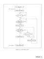
CHECK DEVICE
Write a command
parameter
to DTR
Read a result
parameter
from DTR
Write 'HSL-US'
Read SSB3
Next
process
Figure 6-33.
CHECK DEVICE STATUS Command Execution Flowchart
HITACHI 39
CHECK INTERRUPT
STATUS command
Read a result
parameter
from DTR
IVC: Invalid command
Read SSBO
>-No______F_D_C-,has an FDD status
FDC has no FDD
Read a result
parameter
from DTR
Figure 6-34.
40 HITACHI
Read PCN
CHECK INTERRUPT STATUS Command Execution Flowchart
SPECIFY 1, 2
corrunand
write a corrunand
parameter
to DTR
Figure 6-35.
SPECIFY 1, SPECIFY 2 Corrunand Execution Flowchart
HITACHI 41
Figure 6-36.
SLEEP Command Issue Flowchart
Next
process
Figure 6-37.
42 HITACHI
ABORT Command Issue Flowchart
6.5
6.5.1
COMMAND FUNCTIONS
READ DATA
Bit
D7
MT
r------~~-------- r--~-------
Command Code
Command
Parameters
x
D6
MM
D5
SD
x
x
--~---
D4
D3
D2
DI
0
0
1
1
0
x
HSL
US 1
US 0
----
~--
x
~
CA
.
HA
..
.
SA
•
~
RL
ESN
..
~
~
Result
Parameters
Do
.
..
..
..
.
..
•
GSL
MNL
S SB0
..
..
..
SSB1
..
..
..
SSB2
CA
,.
,.
,.
HA
SA
..
..
•
RL
Figure 6-38.
READ DATA Command
The READ DATA command (figure 6-38) transfers data to the host from the disk.
The command parameters specify the location of the data on the disk.
sector read is automatically performed.
Multi-
Multitrack read can also be performed
if specified.
Selection of Unit and Head:
When the command execution begins, a unit (drive)
and a head are selected according to the command parameters.
Ready Check:
The ready signal from the drive is checked after waiting for
more than 3 Ws following the drive selection.
If the drive is not ready, the
DNR (drive not ready) bit of SSBO is set and the command execution is abnormally
terminated.
Head Load:
The ready check is also performed during an ID search.
If the heads of a selected drive are not already loaded, they are
automatically loaded on the disk and the command is executed after waiting for
the head load time specified by the SPECIFY command.
If the heads are already
loaded, the FDC does not wait for the head load time.
ID Search:
The FDC searches for the ID specified in the command parameters.
If an ID different from the specified ID is found, a CRC check is performed for
HITACHI 43
the ID.
If the ID address mark cannot be found by the time three index
pulses are detected, the ANF (AM not found) bit of SSBI is set and the
command execution is abnormally terminated.
Even after an ID address mark
is found, if the specified ID cannot be found by the time three index pulses
are detected, the INF (ID not found) bit of SSBI is set and the command
execution is abnormally terminated.
If the found ID's CA (cylinder address)
byte does not match the desired ID's CA byte, the result parameters are set
as follows depending on the contents of the command parameter CA byte .
. The loaded CA
=
HEX FF:
BDC (bad cylinder) bit of SSB2 as well as the INF
bit are set and the command execution is abnormally terminated .
. The loaded CA
t-
HEX FF:
CAD (cylinder address unmatch) bit of SSB2 as well
as the INF bit are set and the command execution is abnormally terminated.
CRe Check:
CRC check is performed every time an ID and data are read.
When a CRC error is detected in an ID field, the CER (CRC error) bit of SSBI is
set and the command execution is abnormally terminated.
When a CRC error is detected in a data field, the CDF (CRC error in data field)
bit of SSB2 as well as the CER bit of SSBI are set and the command execution is
abnormally terminated.
Detection of Data Address Mark:
The NAM (no data address mark) bit of SSB2 as
well as the ANF (AM not found) bit of SSBI are set and the command execution is
abnormally terminated in the following two conditions: a data address mark is
not found within 1 ms after a CRC check on the specified read ID, or the first
data other than HEX 00 found after the desired ID and at least 4 bytes (FM
mode) or 5 bytes (MFM mode) of HEX 00 were detected is not AM.
Detection of Deleted Data Address Mark:
(data address mark: HEX FB
When a deleted data address mark
deleted data address mark: HEX FB) is detected,
the DDA (deleted data address mark) bit of SSB2 is set.
If the SD (skip
DDAM) bit of the command code is 0, the data in the sector is transmitted
and the command execution is normally terminated.
If the SD bit is 1, the
data in the sector is skipped (not transmitted, not CRC checked in the data
field) and the FDC starts to process the next sector.
Data Transmission:
The FDC requests the host to accept the data read from
a disk in one of two ways depending on the NDM bit of the SPECIFY command.
Data transmission is requested by the DREQ signal in DMA mode or by the IRQ
signal in Non-DMA mode.
44 HITACHI
If the host does not access the data in the data
register within the periods shown in table 6-S after the data transmission
request, the DOR (data overrun) bit of SSBl is set, a CRC check is performed
on the sector data read and the command is abnormally terminated.
Table 6-S.
Read Data Transfer Request wait Times
8"/5" (pin 6)
FM mode
MFM mode
Low
54 )Js
22 )Js
High
27 )Js
11 )Js
Multisector/Multitrack Read:
If the i:5E'ND signal is not received even after
the last byte 6f a sector has been transmitted to the host, SA is incremented
and the FDC starts to process the next sector (multisector read).
However, if SA of the processed sector is ESN, the following operations are
performed depending on the Head Address HA and the MT bit of the command code.
MT bit
=
1 and HA
HEX 00:
SA and HA are set to HEX 01 and a multitrack
read is performed.
MT bit
=
0 or HA
=
HEX 01:
The NDE (No DMA end) bit of SSBI is set and the
command execution is abnormally terminated.
When the DEND signal is received in the middle of a sector data transfer, the
data transmission to the host stops immediately.
However, the rest of the
sector data is read from the drive and its CRC bytes are checked.
If there
exists no CRC error, the command execution is terminated normally.
Also, when
the DEND signal is received during the transmission of the last byte of a
sector, access of the next sector is not performed and the command execution
is terminated normally.
If the DEND signal is received within the time shown
below after a data transmission request, transmission of the next data byte is
not performed.
For DEND signal received during the transmission of a byte in the middle of
a sector, see table 6-9.
Table 6-9.
BEND in the Middle of a Sector
S"/5" (pin 6)
FM mode
MFM mode
Low
59 lls
27 )Js
High
27 )Js
11 )Js
For DEND signal received during the transmission of the last byte of a
sector, see table 6-10.
HITACHI 45
DEN5
Table 6-10.
at the Last Byte of a Sector
8"/5" (pin 6)
Low
FM mode
MFM mode
128 l1sec
64 l1sec
64 l1sec
32 l1sec
High
Head Unload Time:
The head loaded state is maintained for the period specified
by the head unload time after the command execution is terminated.
Con-
sequently, during this period if a command is issued for the same cylinder of
the same drive, it can be executed before the head load wait time.
Transmitting Only the Number of Bytes Specified by MNL from a Sector:
command parameter's RL byte
=
with
HEX 00 and MNL byte < HEX 80, only the bytes
specified by the MNL byte are transmitted from each sector.
Remaining bytes
are checked for a CRC error, but they are not transmitted to the host.
until the DEND signal is received, a multisector read is performed with only
MNL bytes being transmitted from each sector.
Result Parameters CA, HA; SA, and RL after Normal Termination with
5EN5
Signal:
When the command execution is normally terminated by the DEND signal, the result
parameters CA, HA, SA, and RL take on the values shown in table 6-11 depending
on the values of the MT bit in the command code, ESN of the command parameters,
and SA of the sector to which the DEND signal was applied.
CAd, HAd, SAd, and RLd represent the ID of the sector, the DEND signal was
applied to.
Table 6-11.
Result of
BEND Termination
Result parameters
SAd
MT
HAd
CA
HA
SA
RL
SAd < ESN
x
x
CAd
HAd
SAd + 1
RLd
SAd > ESN
0
x
CAd + 1
HAd
HEX 01
RLd
HEX 00
CAd
HEX 01
HEX 01
RLd
HEX 01
CAd + 1
HEX 00
HEX 01
RLd
1
Note:
x
46 HITACHI
Don't care
6.5.2
READ DELETED DATA
Bit
Command Code
Command
Parameters
D7
MT
D6
MM
D5
SD
D4
D3
D2
D.
Do
0
1
1
0
0
x
x
x
x
x
HSL
USl
USo
..
II
HA
.•
SA
II
II
II
..
RL
ESN
II
II
GSL
MNL
...
II
S S B0
II
II
SSB1
..
II
S SB2
II
CA
..
..
Result
Parameters
II
CA
II
II
HA
SA
II
RL
Figure 6-39.
II
II
..
..
II
READ DELETED DATA Command
The READ DELETED DATA command (figure 6-39)
is identical to the READ DATA command
except that HEX FB and HEX F8 are regarded as the deleted data address mark and
the data address mark, respectively.
HITACHI
47
6.5.3
READ ERRONEOUS DATA
Bi t
D7
D6
D5
D4
D3
D2
D\
Do
Command Code
0
MM
0
0
0
0
1
0
Command
Parameters
x
x
x
x
x
HSL
US 1
..
Result
Parameters
USO
CA
III
HA
III
SA
..
•
•
•
•
•
•
..
III
RL
ESN
III
GSL
III
MNL
III
SSB0
III
SSB1
III
SSB
CA
..
..
HA
...
III
SA
..
RL
..
Figure 6-40.
..
•
..
2
•
•
READ ERRONEOUS DATA Command
The READ ERRONEOUS DATA command (Figure 6-40) reads the data starting from
the first sector detected after the index to the end of the track regardless
whether there are errors present or not.
Sectors are read in the order, they
occur after index pulse detection, independent of CA, HA, SA and RL.
The SA
byte of the command parameters is ignored and HEX 01 is specified in the FDC
at the start of the command execution.
incrementing SA by 1.
Selection of Unit and Head:
Ready Check:
Multisector read is performed by
Multitrack read cannot be specified.
Same as in the READ DATA command.
Same as in the READ.DATA command.
Head Load:
Same as in the READ DATA command.
ID Search:
An ID following the index pulse is searched independent of the
command parameters.
The FDC uses CA, HA, and RL just as set in the command parameters but ignores
SA and sets it to HEX 01 to begin the ID search.
If the contents of an ID
field following the index pulse do not match the specified CA, HA, SA, and
RL, the INF bit of SSBI is set.
Simultaneously, the data in the sector is
read and SA is incremented to search for an ID in the next sector.
48 HITACHI
If the
CA byte does not match, only the INF bit of SSBI is set.
Although an ID
mismatch is detected, the command execution is not abnormally terminated.
If an ID address mark cannot be found by the time three index pulses are
detected, the ANF bit of SSBI is set and the command execution is abnormally
terminated.
CRC Check:
CRC check is performed every time an ID and data are read.
When
a CRC error is detected, the CER bit of SSBI and the CDF bit of SSB2 are set
in the same way as in the READ DATA command.
CRC error detection does not
cause abnormal end of the command execution.
Detection of Data Address Mark:
Same as in the READ DATA command.
Detection of Deleted Data Address Mark:
detected, the DDA bit of SSB2 is set.
When a deleted data address mark is
Data on a sector containing a
deleted data address mark is also accessed.
Detection of a deleted data
address mark does not cause the command execution to terminate.
Data Transmission:
Multisector Read:
Same as in the READ DATA command.
Multisector read is performed in a sequential order as
they physically occur after the index pulse.
received, the read operation stops.
When the DEND signal is
SA is initially set to HEX 01
independent of the contents of any ID read and is incremented by 1 for
every sector read.
All other operations are the same as in the READ DATA command.
The READ ERRONEOUS DATA command has no multi-track read function.
Head Unload Timing:
Same as in the READ DATA command.
Transmitting Only the Number of Bytes Specified by the MNL from a Sector:
Same
as in the READ DATA command.
Result Parameters CA, HA, SA, and RL after Normal Termination by DENB Signal:
Same as in the READ DATA command.
HITACHI 49
6.5.4
READ ID
D7
D6
Command Code
a
MM
a
a
1
a
1
a
Command Parameters
X
X
X
X
X
HSL
US 1
USa
Bit
Resu1 t
Parameters
..
..
..
..
..
..
D5
D4-
D3
D2
DI
•
•
•
•
•
•
•
SSBa
SSB
1
SSB
2
CA
HA
SA
.
RL
Figure 6-41.
Do
READ ID Command
The READ ID command (figure 6-41) transmits the first error-free ID detected
after the command execution has started to the host as result parameters CA,
HA, SA, and RL.
Selection of Unit and Head:
Ready Check:
Same as in the READ DATA command.
Same as in the READ DATA command.
Head Load:
Same as in the READ DATA command.
ID Search:
The FDC searches for a CRC error-free ID.
If an ID address mark cannot be found by the time three index pulses are
detected, the ANF bit of SSBI is set and the command execution in abnormally
terminated.
If a CRC-error-free ID cannot be found by the time three index
pulses are detected, even if an ID address mark has been found, the INF
(ID Not Found) of SSBI is set and the command execution is abnormally terminated.
CRC Check:
A CRC check is performed on the read ID.
If an error exists
the SSBO byte is not modified, but the next ID is searched.
Head Unload Timing:
50 HITACHI
Same as in the READ DATA command.
6.5.5
WRITE DATA
Bi t
Command Code
Command
Parameters
D7
MT
D6
MM
D5
D4
D3
D2
D.
Do
0
0
0
1
0
1
x
x
x
x
x
HSL
1
USa
CA
•
"
HA
SA
•
III
"
RL
II
ESN
GSL
..
..
..
..
..
•
III
MNL
S SBa
III
SSB1
•
•
SSB2
•
•
III
Result
Parameters
US
...
.
CA
III
...
..
HA
SA
•
..•
RL
III
Figure 6-42.
WRITE DATA Command
The WRITE DATA command (figure 6-42) requests the data transfer from the
host and writes it to a sector on a track specified by the command parameters at the current head position.
performed.
Multisector write is automatically
Multitrack write can also be performed if specified.
Selection of Unit and Head:
Ready Check:
Same as in the READ DATA command.
Same as in the READ DATA command.
Head Load:
Same as in the READ DATA command.
ID Search:
Same as in the READ DATA command.
CRC Check:
CRC is checked every time an ID is read.
If a CRC error is
detected, the CER bit of SSBI is set and the command execution is abnormally
terminated.
Writing a Data Address Mark:
One-byte and four-byte data address marks are
written in the FM and MFM modes respectively.
FM mode
Data:
Clock:
HEX FB
HEX C7
HITACHI
51
MFM mode
Data:
HEX Al HEX Al HEX Al HEX FB
Clock:
HEX OA HEX OA HEX OA HEX 00
Transmitting Data:
According to the NDM bit of the SPECIFY command, data
transmission is requested from the host by the DREQ (DMA mode) or IRQ signal
(Non-DMA mode).
The data from the host are written to the disk in order of
upper bits to lower bits.
If the host does not transmit the data within the
times shown in table 6-12 after a transmission request by the DREQ or IRQ
signal, the DOR bit of SSBl is set and the command execution is abnormally
terminated.
Table 6-12.
Write Data Transfer Request Wait Times
8"/S" (Pin 6)
FM Mode
MFM mode
Low
52 l-ls
20 l-ls
High
26 l-ls
10 l-ls
Multisector/Multitrack Write:
If the DEND signal is not received after all the
data for one sector has been transmitted from the host, SA is incremented by 1
and processing of the next sector begins (multisector write).
However, if
SA of the last sector processed is ESN, the following operations are
performed depending on the Head Address HA and the MT bit of the command code:
MT bit
=
1 and HA
HEX 00
Multitrack write is performed with SA
. MT bit
=
0 or HA
=
HEX 01, HD
HEX 01 .
HEX 01
The NDE bit of SSBl is set and the command execution is abnormally terminated.
If the DEND signal is received during the transmission of the data bytes for
a sector, the data transmission request to the host ends immediately and HEX 00
is written for the remaining data bytes; the command execution is normally
terminated.
Also, when the DEND signal is received during the transmission
of the last byte for a sector, access of the next sector is not performed
and the command execution is normally terminated.
Valid input timing of
the DEND signal is the same as in the READ DATA command.
Head Unload Timing:
Same as in the READ DATA command.
Transmitting Only the Number of Bytes Specified by MNL to a Sector:
command parameter RL byte
=
with the
HEX 00 and MNL byte < HEX 80, only the number of
bytes specified by the MNL byte is requested to be transmitted to a sector.
52 HITACHI
HEX 00 is written for the remaining bytes.
Until the DEND signal is
received, a multisector write is performed with only MNL bytes being
transmitted for each sector.
Result Parameters CA, HA, SA, and RL after Normal Termination with DEND Signal:
Same as in the READ DATA command.
Checking Write Protected Signal:
The write protected signal is checked
immediately after the ready signal check.
If a write protected signal is
active, the WPM (write protected medium) bit of SSBl is set and the command
execution is abnormally terminated.
Checking Write Fault Signal:
The write Fault signal is checked when the write
gate signal is deactivated after the data has been written into a sector. If the
write fault signal is active, the DER (drive error) bit of SSBO is set and
the command execution is abnormally terminated.
writing CRC and Data Gap:
CRC and a
l~byte
A data field write is completed by writing a 2-byte
data gap at the end of the data field.
signal is deactivated.
Then the write gate
The contents of the CRC bytes are calculated based
on the data transmitted from the host.
The contents of the data gap are:
FM mode:
MFM mode:
HEX FF
HEX 4E
HITACHI 53
6.5.6
WRITE DELETED DATA
Bit
Command Code
Command
Parameters
D7
D6
D5
D4
D3
D2
D\
Do
MT
MM
0
0
1
0
0
1
x
x
x
x
x
HSL
USI
USo
.
CA
..
..
..
HA
SA
RL
ESN
GSL
MNL
SS B0
SSB1
,.
,.
•
Result
Parameters
.
..
..
..
.,
..
.,
..
..
.
.,
.,
.,
.,
III
SSB2
CA
HA
SA
.,
.,
III
RL
...
.
Figure 6-43.
..
WRITE DELETED DATA Command
The WRITE DELETED DATA command (figure 6-43) is identical to the WRITE DATA
command except that the following i-byte and 4-byte deleted data address marks
are written in the FM and MFM mode, respectively.
In FM mode
Data
HEX F8
Clock:
HEX C7
In MFM mode
Data :
HEX Ai, HEX Ai, HEX Ai, HEX F8
Clock:
HEX OA, HEX OA, HEX OA, HEX 03
54 HITACHI
6.5.7
WRITE FORMAT
Bi t
Connnand Code
Connnand
Parameters
D7
a
x
D6
MM
D5
a
D4a
x
x
x
..
.
D2
DI
Do
1
1
a
1
x
HSL
USI
USa
RL
SCNT
..
..
..
Result
Parameters
D3
GP3L
DUD
S SBa
r----
...
S SB1
.
.
.
S SB2
CA
HA
.
SA
..
RL
Figure 6-44.
..
..
..
..
.
..
.
..
.,
..
..
WRITE FORMAT Connnand
The WRITE FORMAT command (figure 6-44) formats a single track where the head is
currently positioned depending on the SFORM input (pin 4).
SFORM
1:
IBM format
SFORM
0:
ECMA (ISO) format
See section 6.6, "Track Format".
When an index pulse is detected, the
write gate signal is activated to begin the formatting operation.
Drive and Head Select:
Ready Check:
Head Load:
Same as in the READ DATA command.
Same as in the READ DATA command.
Same as in the READ DATA command.
Head Unload Timing:
Same as in the READ DATA command.
Write Protected Signal Check:
Write Fault Signal Check:
Same as in the WRITE DATA command.
A write fault signal check is performed immediately
after the write gate signal is deactivated at the end of each track formatting.
At this time if the write fault signal is active, the DER bit of SSBO is set and
the command is abnormally terminated.
Formatting Start and End:
Formatting begins when the index pulse is detected.
After the last sector has been written, the gap is written continually until
HITACHI 55
the next index pulse is detected.
When the next index pulse is detected, the
formatting operation ends by deactivating the write gate signal.
Note:
When the second index pulse is detected, the write gate signal is
deactivated even if the last sector write has not yet been completed and the
command is normally terminated.
Data Transfer:
During formating, ID field's CA, HA, SA, and RL bytes must be
transferred as data for each sector.
possible.
Both DMA and Non-DMAtransfers are
Data transfer timing is the same as in the WRITE DATA command.
If
the data transfer from the host is delayed and cannot meet the transfer request
made by the FDC's IRQ or DREQ signal, the DOR bit of SSBI is set and the
command is abnormally terminated.
The FDC continues to write the gap from the
time an overrun error occurred (in the middle of an ID field) until the next
index pulse is detected.
The CA, HA, SA, and RL bytes from the transferred
data are written intact into the ID field.
Therefore, even if command
parameter's RL byte value is different from the transferred data's, the
transferred data's RL value is written in the ID field.
The actual sector
length, however, complies with command parameter's RL byte rather than the
RL byte on the disk.
Format:
Format conforms to section 6.6, "Track Format". Sector length is
specified by the command parameter's RL byte.
The number of sectors to be
written is specified by the SCNT (sector count) byte.
byte's contents are written into all data fields.
The DUD (dummy data)
Length of the gap between
the adjacent sectors (GAP3) is specified by the GP3L (gap 3 length) byte.
56 HITACHI
6.5.8
SEEK
D7
D6
D5
D4-
D3
D2
Dl
Command Code
0
0
0
0
1
1
1
1
Command
parameter
x
x
x
x
x
x
US 1
usa
Bit
..
Do
NCN
---
Result parameter
Figure 6-45.
SEEK Command
In the SEEK operation (figure 6-45), a drive's head is moved onto the track
specified by the command parameter's NCN (New Cylinder Number) byte.
The
stepping rate (step pulse interval) is specified by the SPECIFY command.
Ready Checking:
Timing for the ready check conforms to section 5, "Polling".
If the ready signal of the drive selected is inactive at the start or during
the command execution, the step pulse output is halted immediately, and the
SED (seek end) and DNR (drive not ready) bits of SSBO are set.
The command is
terminated abnormally and a request for issuing the CHECK INTERRUPT STATUS
command is made by setting the IRQ signal active.
Drive Seek Bits Setting:
After the ready signal has been checked, the drive
seek bit (DOS-D3S) of the status regi"Ster (STR) corresponding to the drive for
which the command was issued is set.
The drive seek bits can be reset only by
issuing the CHECK INTERRUPT STATUS or ABORT command after the seek operation.
Direction Signal (HDIR) Setting:
Command parameter's NCN and FDC's PCN
(physical cylinder number) bytes are compared:
If NCN > PCN, HDIR is set
If NCN < PCN, HDIR is reset
HDIR is undefined (lor 0) when NCN=PCN
PCN Setting:
Step pulse count is calculated from the PCN and NCN values after
which the NCN value is substituted for PCN.
Accordingly, the head's actual
physical address will differ from the PCN value if a command ends (abnormal end
due to change in state of ready signal, or end by ABORT command) before all
step pulses are issued.
The head's physical address will also differ from the
PCN value if a second SEEK command is issued to a drive while it is seeking.
When issuing the SEEK command, make sure that the drive seek bit of the status
register corresponding to the drive to which the command is issued is zero.
HITACHI 57
Seek Completion:
After all the calculated number of step pulses have been
output, SSBO's SED (seek end) bit is set after the step rate time specified by
the SPECIFY command following the last step pulse output.
The number of the
drive which terminates the seek is then set in USO and USI of SSBO.
Following
this, the command terminates normally and the CHECK INTERRUPT STATUS command
is requested by setting the IRQ signal active.
Additionally, when HDIR=O,
if TRKO becomes active, the step pulse output is halted prematurely.
Following this, as described in the previous paragraph, the SED,
usa,
and
USI bits of SSBO are modified and the command normally ends with an interrupt request to the host for issuing a CHECK INTERRUPT STATUS command.
At this time, the result parameter PCN of the CHECK INTERRUPT STATUS
command is the same as the command parameter NCN value of the SEEK command,
and is not always HEX 00.
I
~s
The TRKO signal is latched 500 ns (8" mode) or
(5" mode) before the step pulse output.
Parallel Seek:
The FDC is placed into the command waiting state when the step
pulse output begins after receiving the SEEK or RECALIBRATE command.
At this
time, another SEEK or RECALIBRATE command can be issued for a new drive whose
drive seek bit in the status register is zero.
Head Unload:
The head must be unloaded (HLOAD
command is issued.
0) immediately after the SEEK
However, if the SEEK command is issued for a drive whose
head is loading and parameter NCN is equal to PCN, the command is terminated
without head unload.
Note:
If the SEEK command is issued to a drive which is not ready, the status
register's drive seek bit is not set.
58 HITACHI
6.5.9
RECALIBRATE
Bit
D7
D6
D5
D4-
D3
D2
1
1
US 1
USO
Command Code
0
0
0
0
0
1
Command Parameter
x
x
x
x
x
x
Result Parameter
D1
Do
--
Figure 6-46.
RECALIBRATE Command
The RECALIBRATE command (figure 6-46) moves a drive's head to track O.
Head
movement speed is the stepping rate (step pulse interval) specified by the
SPECIFY command.
Ready Checking:
Same as in the SEEK command.
Drive Seek Bit Setting:
Same as in the SEEK command.
Direction Signal Setting:
PCN Setting:
Resets HDIR.
Step pulse count is 255, and PCN
=
HEX 00.
However, if the
system is in the drive-not-ready state, the PCN value does not change.
End of Recalibration:
If the TRKO signal becomes active during recalibration
or after the step rate period specified by the SPECIFY command following the
255th step pulse, SSBO's SED bit is set and the recalibrated drive number
is set in
usa
and USl and the command ends normally.
Following this, a
request for the CHECK INTERRUPT STATUS command is made to the host by
setting the IRQ signal active.
If the TRKO signal does not become active
following the step rate time specified by the SPECIFY command after 255
step pulses, SSBO's SED and DER (drive error) bits are set,
usa
and USl are
set to the recalibrated drive number, and a CHECK INTERRUPT STATUS command
is requested by setting the IRQ signal active.
Parallel Seek:
Head Unload:
Same as in the SEEK command.
Head unload state (HLOAD
0) is specified immediately after the
RECALIBRATE command is issued.
Note:
If the RECALIBRATE command is issued to a drive which is not ready, the
status register's drive seek bit is not set.
HITACHI 59
6.5.10
COMPARE EQUAL
Bit
Command Code
D7
D6
MT
x
Command
Parameters
D5
D4
D3
D2
D\
Do
MM
SD
1
0
0
0
1
x
x
x
x
HSL
US 1
USo
..
..
CA
HA
..
SA
..
...
RL
ESN
..
STEP
.
GSL
..
..
Result
Parameters
SSB0
SSB1
..
..
..
II
..
..
..
..
..
..
SSB2
..
CA
•
...
..
HA
SA
•
Figure 6-47.
II
RL
..
..
II
COMPARE EQUAL Command
The COMPARE EQUAL command (figure 6-47) compares data from the host with the
data read from a disk.
Drive and Head Select:
Ready Check:
Same as in the READ DATA command
Same as in the READ DATA command
Head Load:
Same as in the READ DATA command
ID Search:
Same as in the READ DATA command
CRC Check:
Same as in the READ DATA command
Data Address Mark Detect:
Same as in the READ DATA command
Deleted Data Address Mark Detect:
Data Transfer:
Same as in the READ DATA command
Same as in the WRITE DATA command except for the values of the
time from the data transfer requests made by the DREQ or IRQ signal to the data
overrun shown in table 6-13.
60 HITACHI
Table 6-13.
Data Overrun Times
8"/S" (Pin 6)
FM mode
MFM mode
Low
43 l1s
15 l1s
High
21 l1s
7 l1s
Multisector/Multitrack Compare:
SA is updated by SA + STEP (command parameter's
STEP byte) to locate the next sector which may satisfy the compare condition;
the sector is then processed in multisector comparison.
However, if the
processed sector's SA is ESN, or SA + STEP> ESN, the following is performed
depending on HA and the command code MT bit:
When MT bit
=
=
1 and HA
HEX 00
Multitrack comparison is performed with SA
When MT bit
=
1 or HA
=
HEX 01, and HA
HEX 01.
HEX 01
CNS (compare condition not satisfied) bit of SSB2 is set and the command ends
normally. In COMPARE commands, ESN
~
HEX FD.
If the DEND signal is received in the middle of sector processing, obtained
data comparison results are checked whether or not they satisfy the specified
condition.
If the condition is not satisfied, the comparison data for the
remaining sector data are not requested by the host to be transferred.
the data from the drive is read and the CRC check is performed.
Still,
However, the
transfer of the comparison data for the next sector indicated by the SA
increment is requested.
That is, the DEND signal is not a command execution
termination condition, so the DEND signal need not be activated at the end of a
sector processing.
A multisector comparison requires that all sector comparison data for all
sector comparison results is to be transferred to the host.
DEND signal valid timing is shown in table 6-14.
Table 6-14
DEND
8"/5" (Pin 6)
in the Middle of a Sector
FM mode
MFM mode
Low
45 l1s
15 l1s
High
21 l1s
7 l1s
Head Unload Timing:
Same as in the READ DATA command
Result Parameter's CA, HA, SA and RL Bytes after a Normal End:
Sector ID
contents which determined a normal end are output to the host.
HITACHI 61
Comparison Condition:
When the data sent from the host matches the data read
from the drive, the compare condition is considered to be satisfied.
HEX FF
data from the host is considered to match any data from the drive, so the
compare condition is always satisfied.
When a specified condition is
satisfied, CCS (compare condition satisfied) bit of SSB2 is set and the
command normally ends.
If no seqtor satisfying the specified conditions is
detected, even if comparison is performed as far as the sector specified by the
ESN byte, the command is completed normally by setting the SSB2 1 s CNS (Compare
Condition Not Satisfied).
62 HITACHI
6.5.11
COMPARE LOW OR EQUAL
Bit
Command Code
Command
Parameters
Result
Parameters
D7
MT
x
D6
MM
x
D5
SD
x
D4
1
x
D3
1
x
II
CA
•
HA
II
SA
II
RL
II
ESN
~
GSL
~
STEP
•
SSBa
II
SSB1
SSB2
.
..
..
..
.
Figure 6-48.
D2
DI
0
a
Do
1
HSL
US 1
USa
..
•
..
..
..
.
..
..
CA
..
.
..
HA
SA
..
RL
..
..
COMPARE LOW OR EQUAL Command
The COMPARE LOW OR EQUAL command (figure 6-48) is identical to the COMPARE EQUAL
command except for the comparison condition.
Comparison Condition:
When the data from the host matches the data from the
drive, the same processing as in the case of COMPARE EQUAL command is performed.
If the data from the host is HEX FF, any data from the drive is considered to
match.
If the first pair of bytes which do not match satisfied the follow-
ing condition:
host data
>
drive data,
the CRC check is performed before ending the command normally.
the CCS bit of SSB2 is not set.
In this case,
If no sector satisfying the specified condi-
tions is detected, even if comparison is performed as far as the sector
specified by the ESN byte, the command is completed normally by setting the
SSB2's CNS (Compare Condition Not Satisfied).
HITACHI 63
6.5.12
COMPARE HIGH OR EQUAL
Bi t
Command Code
Command
Parameters
D6
D7
MT
x
MM
x
D5
SD
x
D4
D3
D2
Dl
1
1
1
0
1
x
x
HSL
USI
USo
..
.
..
CA
•
HA
..
RL
•
•
•
..
ESN
GSL
•
SA
..
..
..
Result
Parameters
Do
STEP
SSBO
.
SSB1
..
SSB2
..
..
..
CA
HA
SA
..
RL
Figure 6-49.
..
...
..
..
..
..
..
..
..
COMPARE HIGH OR EQUAL Command
The COMPARE HIGH OR EQUAL command (figure 6-49) is identical to the COMPARE
EQUAL command except for the comparison condition.
Comparison Condition:
When the data from the host matches the data from the
drive, the same processing as in the case of COMPARE EQUAL command is performed.
If the data from the host is HEX FF, any data from the drive is considered to
match.
It the first pair of bytes which do not match satisfies the following
condition:
host data
<
drive data,
the CRC check is performed before ending the command normally.
the CCS bit of SSB2 is not set.
In this case,
If no sector satisfying the specified condi-
tions is detected, even if comparison is performed as far as the sector
specified by the ESN byte, the command is completed normally by setting the
SSB2's CNS (Compare Condition Not Satisfied).
64 HITACHI
6.5.13
CHECK DEVICE STATUS
Bit
Command Code
CornmandParameters
D7
D6
D5
D..
Da
D2
Dl
Do
0
0
0
0
0
1
0
0
x
x
x
x
x
HSL
Figure 6-50.
US
1
USO
S SB3
Result Parameters
CHECK DEVICE STATUS Command
The CHECK DEVICE STATUS command (figure 6-50) reads the status of a drive and
sets it up in SSB3 transfer to the host.
HSL, USI and
usa
bits of SSB3 are
updated to contain exactly the same values as the respective command parameter values.
This command can also be issued for a drive which is performing
a seek or recalibrate operation.
If the command is issued for a different
drive than the one currently selected, then its heads must be immediately
unloaded (HLOAD
=
0).
HITACHI 65
6.5.14
CHECK INTERRUPT STATUS
Bit
D7
I D6 I
D5
I
D4
I
Da
D2
Dl
Do
Command Code
0
I
0
I
0
I
1
0
0
0
0
I
CommandParameters
ResultParameters
--
..
Figure 6-51.
SSBO
~
peN
~
CHECK INTERRUPT STATUS Command
The CHECK INTERRUPT STATUS command (figure 6-51) transfers to the host the
causes of the interrupt request made by the FDC, when the status register
value is HEX
ax
(command waiting state).
There are two types of interrupt causes:
. SEEK or RECALIBRATE command has ended normally or abnormally
. Ready signal has changed state since last polling
When the FDC does not have the Seek End (SED) or Ready Inversion (CDS)
status, issuance of the CHECK INTERRUPT STATUS command is treated as an
INVALID command.
66 HITACHI
6.5.15
SPECIFY 1
Bit
Command Code
Command
Parameters
D7
0
I
I
D6
0
I
I
D5
0
I
I
D4
D3
0
0
I
I
STR
D2
0
I
I
DI
I
Do
1
I
1
HDUT
HDLT
I NDM
--
Result Parameters
Figure 6-52.
SPECIFY 1 Command
The SPECIFY 1 command (figure 6-52) specifies the stepping rate, head unload
time, head load time, and Non-DMA mode (or DMA mode).
If a SPECIFY 1 command is issued after a SPECIFY 2 command, the auto-precompensation and high-speed seek modes specified under SPECIFY 2 command are
reset, and the track position activating the LCT signal is specified as track 43.
HITACHI 67
6.5.16
SPECIFY 2
Bit
D7
Command Code
Command
Parameter
0
I
I
D6
I
D5
I
D4-
D3
A
I
H
I
0
1
I
I
STR
D2
I
Dl
I
Do
1
I
1
I
0
HDUT
1
I NDM
HDLT
LCTK
Command
Parameter
PCl
PCO
2
PCDCT
--
Result Parameter
Figure 6-53.
SPECIFY 2
The SPECIFY 2 command (figure 6-53) specifies the stepping rate, head unload
time, head load time, Non-DMA mode, low write current starting track position,
auto-precompensation mode, high-speed seek mode, precompensation delays for
auto precompensation, and precompensation delay change track number.
parameter 1 is required whenever this command is issued.
is needed only when command code bit A
= 1.
When A
=
Command
Command parameter 2
0, the FDC cannot accept
this parameter.
Auto-Precompensation Mode:
selected.
When A
= 1,
the auto-precompensation mode is
In this mode, the write data which has been adjusted for the PCl or
PCO specified precompensation delays is output (only in MFM mode), with the
EARLY (pin 34) and LATE (pin 33) outputs fixed at low level.
When A = 0,
autoprecompensation is not performed, but the EARLY and LATE precompensation
control signals are output (only in MFM mode).
High-Speed Seek Mode:
When H ::: 1, the high-speed seek mode is selected.
This
mode allows the stepping rate to be set to a value ranging from 1 to 16 ms in
1 ms increments in the 5" mode (8"/S"
has no meaning.
68 HITACHI
= low).
In the 8" mode (8"/S"::: high), H
6.5.17
SLEEP
D7
Bi t
Command Code
0
D6
I
I
0
I
I
D5
0
I
I
D40
I
I
Command Parameters,
--
Result Parameters
--
Figure 6-54.
D3
1
I
I
D2
1
I
I
Dl
1
I
I
Do
0
SLEEP Command
The SLEEP command (figure 6-54) allows the FDC to dissipate lower power.
When the FDC receives this command,
1.
HLOAD (Head Load)
is set low,
2.
USO and USl are set high,
and the SLEEP mode is entered.
In this mode, no drive polling is performed.
In the SLEEP mode, the FDC's status register is set to HEX 80 indicating that
the FDC is in the command waiting state.
When the FDC receives a command in
the SLEEP mode, it automatically releases the SLEEP mode and executes the
command.
Power dissipation can be reduced by halting the FDC clock after saving the
status conditions gathered immediately before the SLEEP mode is entered.
HITACHI 69
6.5.18
ABORT
Bit
Command Code
D7
I
D6
1
I
1
r D5
I
1
1
D4-
I
1
1 D3 I
1 I
1
Command Parameters
--
Result Parameters
--
Figure 6-55.
D2
I
Dl
1
1
1
I
I
Do
1
ABORT Command
The ABORT command (figure 6-55) resets the FDC by software.
Note:
This command is issued by writing it into the abort register (ATR) , and
holding RS
= O.
The abort register can be accessed at any time, irrespective of the FDC state,
except when the RESET input signal is active.
When the FDC receives the ABORT command:
1.
FRES, HLOAD, STEP, EARLY, LATE, WDATA, and WGATE signals are set to low
level.
2.
DREQ and IRQ signals are set to high level
3.
Status register (STR) is set to HEX 80 and the drive polling starts.
This command cannot reset FDC's cylinder numbers or the values specified by
the SPECIFY command.
However, when the ABORT command is issued during the
execution of a SEEK or RECALIBRATE command, the cylinder number is the value
set by the SEEK or RECALIBRATE command, although the remaining step pulses
are no longer generated.
Thus, in such a case, a RECALIBRATE command must be
be issued before the next command is issued.
70 HITACHI
6.5.19
READ LONG
Bit
Command Code
Command
Parameters
D7
D6
D5
D4-
D3
D2
DI
MT
MM
SD
1
0
0
1
0
x
x
x
x
x
HSL
USl
USo
..
..
..
•
HA
..
SA
,.
Result
Parameters
•
CA
•
•
•
RL
,.
,.
,.
,.
,.
,.
ESN
GSL
..•
MNL
SSB0
SSB1
SSB
,.
2
CA
,.
HA
,.
r-----
SA
..
RL
Figure 6-56.
Do
•
•
•
•
•
•
READ LONG Command
The READ LONG command (figure 6-56) transfers the 2-byte CRC information as
well as the data read from a sector to the host.
This command is valid
only after a SPECIFY 2 command has been issued.
Otherwise it is invalid.
This command is identical to the READ DATA command with the following two
exceptions:
The CRC bytes of the sector whose data has been just transferred are also
transferred to the host computer.
Data transfer of the type requiring only the number of bytes specified by
MNL from a sector is ignored.
With the
DE~D
signal, however, the data
transfer can be terminated even in the middle of a sector data or CRC byte
transfer.
This command also performs a CRC check for the sector from which the data was
transferred.
HITACHI 71
6.5.20
WRITE LONG
Bit
Command Code
Command
Parameters
D7
D6
D5
D4-
D3
D2
D,
MT
MM
0
1
0
1
1
x
x
x
x
x
..,.
USI
0
US
CA
•
HA
~
..
SA
~
RL
~
...
ESN
~
.
..,.
Result
Parameters
HSL
Do
0
•
SSB1
~
SSB
..
..
..
.
..
.
Figure 6-57.
•
•
GSL
MNL
..
0
SSB2
~
CA
~
..
..
HA
SA
~
RL
WRITE LONG Command
The WRITE LONG command (figure 6-57) writes to a disk the 2-byte CRC information
as well as the data sent from the host.
SPECIFY 2 command has been issued.
This command is valid only after
Otherwise it is invalid.
This command
is identical to the WRITE DATA command except for the following:
The host sends the 2-byte CRC information also for the sector whole
data has just been sent.
Only the number of bytes specified by the MNL byte can be written to a sector.
The CRC byte also must be sent.
If the data transfer is halted in the middle of a sector by the DEN5 signal,
HEX 00 is written into the remaining sector including the CRC bytes.
72 HITACHI
6.5.21
INVALID
Bit
D'j
I
D6
I
Ds
Command Code
I
DIt
I
D3
1 D2
J
D1
J
Do
INV ALID Code
Command Parameters
Result Parameters
---
..
SSBO
Figure 6-58.
INVALID Command
The FDC processes the following cases as an INVALID command (Figure 6-58):
· Undefined command codes are written into the data register (DTR).
· HEX FF is written into DTR as a command.
• Issuing the CHECK INTERRUPT STATUS command when FDC has no Seek-end or
Ready Inversion status informations.
SSBO of the result parameter is HEX 80.
The following codes are not considered as INVALID commands after the SPECIFY 2
command has been issued:
HEX 10, 13, 14, 15, 17, 18, lA, lB, lC, lF, 57, 58
Consequently, if any of these codes is written into the FDC as a command, the
FDC will malfunction.
The ABORT command can be used to bring the FDC to the
command waiting state, but the internal RAM contents may be destroyed.
To prevent this a SPECIFY command followed by the RECALIBRATE command must be
issued before any other command is issued.
Do not write these codes into
FDC as a command at SPECIFY 2 mode.
HITACHI 73
6.6
TRACK FORMAT
Figure 6-59 shows the IBM and ISO track formats
SFORM=1
IBM Format
Index
~----------------------~~----~J~
I
I
Code
(HEX)
4E
Length
(Byte)
80
SFORM=O: ISO Format
Index
n
----~;
.
r--l
~----------------------------~I~
:
One Sector
~
:
I
I
FF
4E
Length
(Byte)
(U) :
(A) :
32
(U): User programmable
(A): Automatically calculated
CA:
HA:
SA:
RL:
Cylinder Address
Head Address
Sector Address
Record Length
IXM : Index Mark
lAM : 10 Address Mark
DAM: Data (Deleted Data) Address Mark
GAP4 length extends from the end of GAP3 in the last sector to the next index pulse.
Codes marked with asterisk ( • ) contain a missing clock.
Figure 6-59.
74 HITACHI
Track Format
6.7
Command Code Rejection
6.7.1
Phenomenon
The FDC rejects command codes under the following timing conditions:
within the period 2.25 us before to 1.75
~s
(1)
after the IRQ signal is asserted
to request a CIS command caused by READY signal inversion in 8-inch mode
~s
(or 4.5
before to 3.5
~s
after IRQ assertion in 5-inch mode); or (2) if
the IRQ signal has been asserted to request a CIS command when READY signal
inversion is detected.
This malfunction is described below for each timing
condition.
Command Rejection Timing Condition 1:
From 2.25
~sbefore
to 1.75
~s
after the IRQ signal is asserted to request a CIS command initiated by the
READY signal in 8-inch mode (or 4.5
~s
before to 3.5
~s
after IRQ assertion
in 5-inch mode)
In 8-inch mode, the FDC rejects all commands except ABORT if those commands
are issued within the period 2.25
to 3.5
~s
~s
before to 1.75
~s
after (or 4.5
~s
before
after in 5-inch mode) the IRQ signal is asserted to request a CIS
command initiated by READY signal
i~version,
as shown in figure 6-60.
time during which commands are rejected is indicated by period A.
tion, for 0.5
~s
(1.0
~s
The
In addi-
in 5-inch mode) (period B) after period A, the FDC
accepts commands but the BSY bit of the status register (STR) remains
cleared.
The BSY bit of the STR is set when the host system writes the
first-byte parameter to the FDC.
Changes in the STR according to the timing
of each issued command are summarized in table 6-15.
Note that the FDC will
not reject a command if the IRQ signal is asserted to request a CIS command
initiated by SEEK or RECALIBRATE command completion.
HITACHI 75
IRQ is asserted to request CIS command
by READY signal inversion
~
1. 75 11s
2. 25 11 s
A
.Figure 6-60.
Notes: 1.
0.5 11 s
B'
~
Command Rejection Timing 1
Figure 6-60 is the timing chart for 8-inch mode.
For 5-inch mode,
the periods must be doubled (2.25 11s + 4.5 11s, 1. 75 ]..ls + 3.5 ]..ls,
and 0.5 11s + 1. 0 ]..ls).
2.
A: If a command is issued during this period, the FDC rejects it.
B: If a command is issued during this period, the FDC accepts it,
but the BSY bit of the STR remains cleared.
76 HITACHI
Command Rejection Timing Condition 2:
The IRQ signal has been asserted to
request a CIS command when READY signal inversion is detected
The FDC rejects commands other than ABORT if those commands are issued when
READY signal inversion has been detected while IRQ is asserted to request
a CIS command initiated by SEEK or RECALIBRATE command completion or by a
READY signal change.
are ignored for 20
~s
As shown by period A in figure 6-61, such commands
in 8-inch mode (40
during period B, which is the 0.5
~s
(1.0
~s
in 5-inch mode).
~s
In addition,
in 5-inch mode) after period
A, the FDC accepts commands, but the BSY bit of the STR remains cleared.
The BSY bit of the STR is .set when the first-byte command parameter is
written by the host system.
IRQ assertion by SEEK or RECALIBRATE command completion
or by a READY signal change
IRQ--------~---------------------------------------------------------
USO
USI
READY
128
128
128
~s
~s
~s
1024
140
~s
160
~s
~s
~--------
READY signal of a drive
changes
Figure 6-61.
Notes: 1.
Command Rejection Timing 2
Figure 6-61 is the timing chart for 8-inch mode.
the periods must be doubled (e.g. , 128
2048
2.
~s,
and 0.5
~s
~s
+ 256
For 5-inch mode,
~s,
1024
~s
+
+ 1.0 ~s) .
A: If a command is issued during this period, the FDC rejects it.
B: If a command is issued during this period, the FDC accepts it,
but the BSY bit of the STR remains cleared.
HITACHI 77
Table 6-15.
STR Changes for Each Command
Issue
Timing
Command
All commands
except CHECK
INTERRUPT
STATUS, SLEEP,
and ABORT
Normal
STR Change
FDC busy
Wait for
command
+
HEX 8X --------
During
period B
+
Normal
+
+
+
+
+
78 HITACHI
t
HEX DX -------Request parameter
acceptance
HEX IX
HEX IX -------- HEX 8X
Ignore command code
HEX IX --------
HEX OX -------- HEX CX
Request
Reset BSY
parameter
acceptance
HEX 10 --------
HEX 80
SLEEP
HEX 10 -------- HEX 80
(Ignore command code)
Do not enter sleep mode
Write command
code
+
HEX 80 --------
Notes: 1.
2.
Accept
parameter
Write command
code
HEX 80 --------
During
period B
HEX IX
HEX 8X
write command
code
HEX 80 --------
During
period A
HEX OX -------Reset BSY
Write command
code
HEX 8X --------
Normal
HEX IX --------
Write command
code
HEX 8X --------
SLEEP
Request
parameter
Write command
code
HEX 8X
During
period B
HEX IX -------- HEX 8X
Ignore command code
Write command
code
HEX 8X --------
During
period A
Request
command parameter
Write command
code
During
period A
CHECK
INTERRUPT
STATUS
Write
parameter
HEX 9X ____ J___ HEX IX
Write command
code
HEX 8X ____ J___ HEX IX
ABORT is always accepted.
X indicates HEX a - HEX F.
HEX 10 --------
HEX 00 -------- HEX 80
Enter SLEEP
Reset BSY
mode
6.7.2
Countermeasures
Hitachi recommends implementing one of the following three countermeasures to
prevent the above malfunctions:
commands);
(1) check the IRQ signal level (valid for all
(2) check the STR status (valid for all commands except SLEEP); or
(3) issue the ABORT command (valid for all command except SLEEP).
These
countermeasures are described in detail below.
IRQ Signal Level Check (valid for all commands)
Whether or not the FDC accepts a command code can be determined by checking
the IRQ signal level after the TXR bit of the STR has been set to 1.
If the
FDC accepts a command code, the IRQ signal is negated high at least 5.5
before the TXR bit is set to 1.
(TXR
=
~s
I indicates command parameter request,
result parameter accept request, or command wait state.)
On the other hand,
if the FDC rejects a command code, the IRQ remains asserted low when the TXR
bit is set to 1.
Therefore, if IRQ is negated high, the next process, such as
a parameter transfer, can be performed correctly; but if IRQ remains asserted
low, the command must be written to the FDC again.
Figure 6-62 shows this
IRQ signal level checking procedure.
HITACHI 79
Command issue start
No
Yes
Yes
Write command
parameter
No
Yes
Command execution
Figure 6-62.
80
HITACHI
IRQ
Signal Level Checking Procedure
STR Check (valid for all commands except SLEEP)
Whether or not the FDC accepts a command code can be determined by checking
the contents of the STR during the T2 state, as shown in figure 6-63.
If the contents of the STR are HEX 00, a command code was issued during
period B shown in figures 6-60 and 6-61.
proces~,
the command code and the next
In this case, the FDC has accepted
such as a parameter transfer, can be
performed after the TXR bit of the STR is checked.
On the other hand, if the contents of the STR are HEX 10, a command code may
be issued during period
and 6-61.
A
or a period other than
A
and B shown in figures 6-60
In this case, whether or not the FDC has accepted the command code
can be determined by the BSY bit of the STR as follows.
(8-inch mode) or 1.2
~s
If BSY is set 0.6
~s
(5-inch mode) after the TXR bit has been set, the FDC
has accepted the command correctly and the next process, such as parameter
transfer, can be performed.
If BSY is cleared, the FDC has rejected the
command and the command code must be issued again.
The STR check procedure is summarized in figure 6-64.
A command code is written
STR
j)
L-
WR
HEX 80
HEX 10
rx
\\
HEX 00
HEX 00
//
T1
Note:
HEX 80 or HEX CO
T2
T1 State
8-inch mode
X
T2 State
5-inch mode
8-inch mode
5-inch mode
Min
Max
Min
Max
unit
Min
Max
Min
Max
unit
o
350
o
600
ns
9.5
18.0
19.0
36.0
~s
STR is HEX 00 during the T2 state if a command code is issued during
period B shown in figures 6-60 and 6-61.
Figure 6-63.
Timing Diagram When STR is HEX 00
HITACHI 81
Command issue start
No
Yes
The STR must be
checked during
the T2 state
shown in
figure 6-63.
Yes
Yes
No
Yes
Wait for
0.6 ].ls (a-inch
mode) or 1. 2 11s
(5- inch mode)
Write command
parameter
No
Yes
No
Yes
Command execution
Figure 6-64.
82 HITACHI
STR Checking Procedure
ABORT Command Issue (valid for all commands except SLEEP)
Whether or not the FDC accepts a command can be determined by checking the BSY
bit of the STR 0.6
~s
~s
(8-inch mode) or 1.2
(5-inch mode) after the TXR bit
has been set.
If a command is issued during period A shown in figures 6-60 and 6-61, the BSY
bit is cleared 0.6
has been set.
~s
~s
(8-inch mode) or 1.2
(5-inch mode) after the TXR bit
In addition, if a command is issued during period B shown in
figures 6-60 and 6-61, the BSY bit is always cleared after the TXR bit has been
set.
Therefore, if the BSY bit is cleared 0.6
~s
(8-inch mode) or 1.2
~s
(5-inch
mode) after the TXR bit has been set, the command must be issued again after
the ABORT command has been issued.
If BSY is set 0.6
~s
(8-inch mode) or 1.2
~s
(5-inch mode) after the TXR bit
has been set, the FDC has accepted a command correctly and the next process,
such as parameter transfer, can be performed.
Figure 6-65 shows the ABORT command issue procedure.
HITACHI
83
Command issue start
Yes
Yes
BSY is
set to 1
by·ABORT
command
Wait for 0.6 lls
(8-inch mode) or
1.2 lls (5-inch mode)
No
Issue ABORT
conunand
Yes
Yes
Write command
parameter
No
Yes
Command execution
Figure 6-65.
84 HITACHI
ABORT Command Issue Procedure
SECTION 7.
VFO CIRCUIT
The VFO circuit (figure 7-1) uses an analog PLL and requires no adjustment and
no external components.
7.1
VFO SYNCHRONIZATION
The VFO synchronizes with the following serial data rates:
FM : 125, 150, 250 kbps
MFM: 250, 300, 500 kbps
To synchronize to the data transferred at 150 kbps in FM or 300 kbps in MFM,
a 19.2 MHz clock must be input to CLK (pin 25) with 8"/5" (pin 6) tied low.
7.2
CONTROLLING THE VFO
The VFO changes the loop gain of the PLL (phase locked loop) while synchronizing
to the SYNC field.
It starts with a high gain to achieve fast synchronization
and switches to a low gain to reduce bit jitter (figure 7-2). While not performing a read operation the VFO synchronizes to the FDC's clock, eliminating
the need for a multiplexed reference clock input on the RDATA pin (pin 30).
During a read operation, when an internally generated SYNC signal becomes
active, the VFO begins to detect an FM/MFM zero pattern on the RDATA (pin 30)
input.
Until detecting a zero, the VFO synchronizes with the FDC's clock.
After detecting one byte of zeros, the VFO starts to synchronize to the RDATA
input with high loop gain.
Synchronization is completed within 3 bytes in FM
mode and 4 bytes in MFM mode, and then the PLL switches to low loop gain.
Now
the FDC determines whether it should read the data or inform the VFO to
resynchronize depending on whether the first non-zero pattern encountered is
an address mark or not.
HITACHI 85
r------- -------------- V F 0 -------- ---- --------,
FDC internal
clock
I
I
I
I
I
I
I
SYNC signal-+----------<p-----t------------,
I
I
I
I
R D A T A--+----.----I
I
CONTROL CIRCUIT
I
I
I
I
I
I
I
I
I
r------Gain switch signal
,----...1--...1...-----,
Compensates for
frequency difference
I
------------------~
I
I
I
I
I
I
Regulated voltage:
I
I
I
Compensates for phase difference
HWINDOW
PLLI
CIRCUIT
I
I
I
WIN DOW - ; - - - - - - - - . - 4
I
I
I
I
Divider
WINDOW
I
I
I
~-------------------------------------Constant
voltage
source
I
----t
I
I
I
I
I
I
REGULATOR
CIRCUIT
I
I
I
I
~--------------------
Figure 7-1.
86 HITACHI
I
_____________________ J
VFO Circuit Block Diagram
Reset FDC
FDC's operation
Reset SYNC signal
NO
NO
Switch PLL gain
FDC's operation {
Detect address mark
Figure 7-2.
VFO Control Flow
HITACHI 87
7.3
PLL CIRCUIT
This PLL circuit, eliminates the need for a noise-sensitive, lag-lead type
filter and instead employs a new system to compensate for phase and frequency
differences.
In this method, frequency differences are compensated using
phase difference measurements.
A constant current source circuit is used
with the charge pump and the VCO (voltage controlled oscillator) circuits
so that supply voltage variations and noise will not influence the PLL.
center frequency of the VCO is 4 MHz.
Separate phase comparators are used
for the SYNC and DATA sections to perform the phase comparisons.
are applied to the phase comparators.
separate the data.
The
Two clocks
One is a WINDOW clock necessary to
The other is a HWINDOW clock with double the WINDOW
frequency which is generated in the process of generating the WINDOW by
dividing the VCO output.
Phase comparison is performed between the center
of the WINDOW and the RDATA input (figure 7-3).
I
v:
WINDOW
i
I
HWINDOW
RDATA
l . . __~
I
Center of WINDOW
~I------------~
n
----------------~I~
~-----------------------
~•.,!-----'--!__ phase difference
Figure 7-3.
88 HITACHI
Phase Comparison
SECTION 8.
WRITE PRECOMPENSATION CIRCUIT
· Digital precompensation circuit
· Delay time programmable by software
· Delay time independently selectable for inner and outer tracks
• Outer to inner switchover track specifiable
· When auto-precompensation mode is not selected by command SPECIFY 2, the
precompensation control signals (EARLY, LATE) are output.
When auto-
precompensation mode is selected, the control signals are not output;
EARLY and LATE are fixed at low level.
· Delay time programmable by 62.5 ns increments
(Note)
· Auto-precompensation and precompensation control signals are output in MFM
mode only
· Range of delay time programmable (in MFM mode)
250 kbps: 0 - 750 ns
300 kbps: 0 - 625 ns (Note)
500 kbps: 0 - 375 ns
When a value beyond this range is specified, FDC may malfunction.
Note: CLK
19.2 MHz, delay time programmable by 52.1 ns increments at 300 kbps.
HITACHI 89
SECTION 9.
9.1
SYSTEM APPLICATION
SYSTEM CONFIGURATION
Figure 9-1 shows a typical system configuration using the HD63265 FDC.
By tying
the IFS pin of HD63265 to high or low, the host interface can be directly
connected respectively to a 68- or 80- series 8-bit system bus.
for data transfer in the DMA mode.
A DMAC is used
Since the HD63265 has on-chip VFO and
write precompensation circuits, the FDD interface requires an oscillator,
a multiplex decoder circuit for decoding the unit select signals, and a
driver/receiver circuit as external circuits.
All signals other than the
unit select and ready signals can be directly connected to the driver/receiver
circuit.
MPU
MAIN
(HD68B09)
MEMORY
ADDRESS BUS
DATA BUS
DMAC
HD63265
(HD68B44)
FDC
FDC
Floppy Disk Controller
MPU
Microprocessing Uni t
DMAC : Direct Memory
Access Controller
Figure 9-1.
90 HITACHI
Typical Configuration of a System Using the HD63265
9.2
SYSTEM OPERATION SEQUENCE
Figure 9-2 shows the operation sequence of a system using the HD63265 FDC.
Host
~_ _~~
Transfer data
Figure 9-2.
F DD
FDC
Perform READ/WRITE
or seek operation
Operation Sequence of a System Using the HD63265 FDC
When READ/WRITE commands are executed, data transfer between a host computer
and the FDC can be performed in the following two modes.
DMA mode in which the DMAC transfers data as a bus master
Non-DMA (PIO) mode in which the CPU transfers data
For operation sequence between the host computer CPU, the DMAC, and the FDC,
refer to section 9.6, "Host Interface".
HITACHI 91
9.3
DATA TRANSFER TIMING
The FDC performs two types of data transfer operations to a floppy disk: one is
a WRITE operation which converts 8-bit parallel data from the host memory to
serial data for writing to a floppy disk, and the other is a READ operation
which converts serial data from a floppy disk to parallel data for transferring
to the host memory.
Therefore, when designing a system with the FDC, the data
transfer timing of the FDD and the data transfer timing of the system must be
coordinated.
9.3.1
READ Operation
Figure 9-3
shows the READ operation timing.
FDD READ
data
FDC data
register
-- - } 2-byte
--------------------~------~------~------~----------------------~----~--~----~--~--~---
delay
IRQ
Non-
DMA
[
CSoR/WoE
(CSoRD)
~t.
DREQ
DMA [ DACKoR/WoE
(DACKoRD)
Note: 80-series signals indicated within parentheses
Figure 9-3.
READ Operation Timing
The serial data transfer rate is --selected by the input level of the 8"/5" pin
and also by the FM/MFM mode.
on the serial data rate.
92 HITACHI
The above timings, tl through ts, vary depending
Table 9-1 shows their variations.
9.3.2
WRITE Operation
Figure 9-4 shows the WRITE operation timing.
IRQ
Non-
DMA
[
CS-R/W-E
(CS-WR)
~
t
~
.~
t6
S
t6
DMA [DREQ
-D-A-C-K~-R~/-W---E----------~
(DACK-WR)
ts
WRITE DATA
FDC data
register
- --I
Ds~DI5
Do~D7
/---
./'-.
\
\
} 2-byte
l
Dg 1__
FDC write data
1--Do 1 Dl 1---1 D7 1 Ds 1
I
I
I
------------~--~--~--~~--+-~~~~--~~~--~--~~
tg=tlOx8
1
t
10
delay
.1
Note: 80-series signals indicated within parentheses
Figure 9-4.
WRITE Operation Timing
As in the case of the READ operation, the above timings t6 through tlO vary
depending on the serial data rate.
9.4
Table 9-1 show their variations, also.
DATA TRANSFER COMPLETION TIMING
During data transfer, the data transfer is completed by asserting the DEND
(transfer completion) signal.
The requirement on the i5ENi5 assertion timing
varies depending on whether it is a READ or WRITE operation, whether
DENB
is
asserted in the middle or at the end of a sector, and what the data transfer
rate is.
9.4.1
The following shows the DEND signal assertion timing for each case.
BEND Signal for READ
BEND Signal in the Middle of a Sector:
Figure 9-5 shows the DEND signal
assertion timing in the middle of a sector.
If the DEND signal is asserted
within tll of a data transfer request made by IRQ or DREQ, further transfer
requests do not occur after transferring the data requested by IRQ or DREQ.
Table 9-2 shows the range of tll depending on the data transfer rate.
HITACHI 93
IRQ or DREQ
CSoR/WoE
or DACKoR/WoE
DATA (Byte)
®
Figure 9-5.
DEN5
®
,-"
------~Do~--------------~DI ~---------------r(~I~-------" • .1
DEND Signal Assertion Timing in the Middle of a Sector
Signal at the End of a Sector:
timing at the last byte of a sector.
Figure 9-6 shows the DEND signal assertion
For transfer request of the last byte of
a sector, asserting the DEND signal within t12 (see Table
9-2) completes
command execution for the sector.
IRQ or DREQ
CSoR/WoE
or DACKoR/WoE
DEND
ILast byte of data in a sector I
DATA (Byte)
Figure 9-6.
94 HITACHI
-----~~------------~d6~--------------------BEND
Signal Assertion Timing at the Last Byte of a Sector
Table 9-1.
FDC Data Transfer Timing
8"/5"
Read
t
MFM
tl
2 "lls
4 "lls
t2
16 "lls
32 "lls
t3
16 "lls
32 "lls
32 "lls
t4
Write
8"/S"
1
FM
0
MFM
FM
Notes
4 "lls
8 "lls
1
32 "lls
64 "lls
1
64 "lls
1
~l
"lls
;;,27 "lls
;;,22 "lls
~54
"lls
~7
"lls
~l
~5
~43
2
"lls
3
t5
16 "lls
32 "lls
32 "lls
64 "lls
1
t6
16 "lls
32 "lls
32 "lls
64 "lls
4
t7
~O
~26
"lls
"lls
~20
"lls
"lls
~52
"lls
"lls
4
4
t8
16 "lls
32 "lls
32 "lls
64 "lls
t9
16 "lls
32 "lls
32 "lls
64 "lls
4
2 "lls
4 "lls
4 "lls
8 "lls
4
tlO
Notes l. For commands READ DATA, READ DELETED DATA, READ ERRONEOUS DATA,
READ LONG, COMPARE EQUAL, COMPARE LOW OR EQUAL, and COMPARE HIGH
OR EQUAL.
2. For commands READ DATA, READ DELETED DATA, READ ERRONEOUS DATA, and
READ LONG.
3. For commands COMPARE EQUAL, COMPARE LOW OR EQUAL, and COMPARE HIGH
OR EQUAL.
4. For commands WRITE DATA, WRITE DELETED DATA, and WRITE LONG.
Table 9-2.
DEND Signal Assertion Timing
8"/S"
MFM
t
Read
Write
Notes:
8"/S"
1
FM
0
FM
MFM
Notes
Middle of
a sector
tll
~l
"lls
S,.27 "lls
~27
"lls
~59
lls
2
Middle of
a sector
tll
~7
"lls
S,.21 "lls
~15
"lls
S,.45 lls
3
End of
a sector
t12
~32
"lls
~64
"lls
~64
"lls
~28
lls
2
Middle of
a sector
t13
~ll
"lls
~27
"lls
~7
"lls
~9
lls
4
End of
a sector
t14
~32
"lls
~64
"lls
~64
"lls
~28
11s
4
See table 9-1.
DEND signal assertion at the end of a sector has no effect on COMPARE commands.
HITACHI 95
DEN5
9.4.2
DEND
Signal for WRITE
Signal in the Middle of a Sector:
If DEND is asserted in the middle of
a sector during a write data transfer, HEX 00 is written in the remaining data
area.
Figure 9-7 shows the DEND signal assertion timing in the middle of a
sector.
If the DEND signal is asserted within t13 of a data transfer request
made by IRQ or DREQ, further transfer requests do not occur after the data
transfer requested by IRQ or DREQ.
The variation of t13 with respect to the
different data transfer rates is shown in table 9-2.
IRQ or DREQ
DATA (Byte)
Do
CS-R/W-E
or DACK-"R/W-E
t
13
DEND
DEN5 Signal Assertion Timing in the Middle of a Sector
Figure 9-7.
DEND
Signal at the End of a Sector:
timing at the last byte of a sector.
Figure 9-8 shows the DEND signal assertion
For transfer request of the last byte of
a sector, asserting the DEND signal within t14 completes command execution for
the sector.
The variation of t14 with respect to the different data transfer
rates is shown in Table 9-2.
IRQ or DREQ
DATA (Byte)
CS-ltjW-E
or DACK-R:/W-E
DEND
Figure 9-8.
96 HITACHI
DEN5
signal Assertion Timing at the Last Byte of a Sector
9.5
FDC CONTROL
9.5.1
FDC Operating States
The FDC has three operating states as follows.
1.
IDLE state:
Usual command wait state
2.
SLEEP mode:
Low power dissipation mode, and also command wait state
3.
Execution state:
9.5.2
State during command execution
Interrupt Servicing
The FOC generates the IRQ signal in the following four cases:
1. Data read/write request in Non-DMA (PIO) mode
2. Result status read request at the termination of READ/WRITE commands
3. Starting request of CHECK INTERRUPT STATUS command at the termination of a
SEEK or RECALIBRATE operation
4. Starting request of CHECK INTERRUPT STATUS command when the READY signal
from an FDD has changed state since it was polled last time.
Thus, a host computer detects IRQ of the FDC, reads the status register,
identifies which of the above cases caused the interrupt, and then services
the request, accordingly.
9.6
HOST INTERFACE
The following examples show how to connect the FDC to the 80-series and
68-series 8-bit bus systems.
9.6.1
80-Series 8-Bit Bus System
Figure 9-9 shows a typical FDC interface circuit for a HD64B180-based
80-series 8-bit bus system.
HITACHI 97
To memory circuit
HD64B180
{(
~
Address Bus Ao-A\/
Ao....... AI8
IOE :>--
~
k
RD
Do
C CS
Yh.
-
G
AO
Do ....... D 7 Knata Bus
HD 6 3 26 5 (FDC)
Address D eco der
(LS138)
DACK
1=---./''-----,
I DACK is generated I
I by decoder because I
L2f.A~.aLaddress~ -1
RS
~
~
~
D7
k
r
D o....... D 7
RD
rWR
WRP
DMRQ h.
e:
TEND ~
~
DREQ
--
INT :>
r
DEND
IRQ
RES
~
RESET
r
Reset
circuit
~CLK
OSC
I
~IFS
TXS
MOTOR
ON
(To FDD interface)
Figure 9-9.
A Typical FDC Interface Circuit Using HD64180 (80-series)
The HD64180 is a CMOS high integration 8-bit microprocessor consisting of a
high-speed CPU, memory management unit (MMU) , DMA controller, timer, asynchronous serial communication interface (ASCI), and serial I/O port.
The MPU
interface is based on the 8080 family (Intel) interface; an E clock is provided
to enable interface with a 6800 family (Motorola) MPU.
In this example,
the
FDC host interface is set to the 8080 family type by tying the IFS pin to low.
HD64180 Address Space:
The HD64180
divi~es
its address space into memory space
(512 kbytes) and I/O space (64 bytes). The FDC is assigned to the I/O space by
connecting the HD64180 IOE pin to the enable (G) pin of the address decode
circuit.
HD64180 I/O Access Timing:
Read/Write operations to the internal registers of
the HD63265 FOC are synchronized with the RO, WR signals of the 80 series.
Therefore, the HD64180 interface should be performed within the specified
setup and hold times of the address, CS and DATA signals.
Figure 9-10 shows the 80-series Non-DMA (MPU) read/write timing of the H063265.
98
HITACHI
CS
RS (Ao )
tAH
tAR
(Wb~)
(min)
PVVimL Ons
RD
fDatalS wrITten
L!!t this edge l
-PW~-~'\
WR
tDDR
(rl~xns)
DATA
Read cycle
\
Figure 9-10.
/
Write cycle
/
80-Series Non-DMA Read/Write Timing of the HD63265
HD63265 timing specifications require minimum setup and hold times of 0 ns for
CS with respect to RD and WR.
However, the HD64180 may not be able to meet
this requirement since the memory and r/o access addresses are decoded
externally, respectively enabled by ME and rOE.
For I/O address decoding, since the address signals (AO to A7) are controlled
by rOE, the resulting r/o access timing of the HD64180 is as shown in figure
9-11.
rn the r/o read cycle, since rOE and RD are asserted simultaneously at
the falling edge of
¢
in state Tl, CS cannot provide setup time for RD.
However, in the read cycle of the HD63265, even if CS is delayed, access time
tDDR is only prolonged up to the CS delay time.
Thus, a sufficient margin
between tDDR and PWRDL enables access.
HITACHI 99
'~HD64180 - l
IOE
I Fetches
Datal
'----------'
Note: WR comes
later than IOE since
it is output from the
rising edge of T2
RD
cs
/1
~
__________________________- J
(.!::..------,
I CS comes later I
LtE an B:~ __
J
WRP
>,
WR
~II
'4
--<
DAT A
DATA OUT (FROM CPU)
r-
tWDH
(min)
40n8
Figure 9-11.
HD64180 I/O Access Timing
Moreover, since data is written to the HD63265 at the rising edge of the WR
pulse, sufficient margin of tWRP enables write as well as read cycles.
(For
details, see HD64180 Hardware Application Note.)
DMA Transfer Mode:
Since the HD63265 has DACK (implicit access), DMA transfer
is possible in single addressing mode.
However, DMA transfer in the case of
HD64l80 employs dual addressing mode in which both the I/O and memory addresses
are generated respectively in an I/O (FDC) read cycle and memory write cycle.
Thus, in response to a DMA request from the FDC, the DACK signal is generated
by I/O address decoding.
Figure 9-12 shows the DMA transfer timing in dual
addressing mode.
CPU Machine
cycle
DMA I/O Read
cycle
DMA Memory
Write cycle
CPU Machine
cycle
DMA cycle in dual addressing mode
DACK
Figure 9-12.
100 HITACHI
DMA Transfer Timing in Dual Addressing Mode
Since the DACK signal of the FDC can replace the CS signal in DMA operation, Tw
(wait) state should be inserted to maintain the FDC read or write access time,
depending on the frequency of
¢
employed.
(For details, refer to HD64180 User's
Manual. )
DMA Transfer Sequence:
Figure 9-13 and 9-14 show the basic sequences of DMA
transfer between the host (HD64180), DMAC (HD64180 built-in DMAC) , and FDC
(HD63265) .
DMAC
(HD64180
built -in)
Host
(HD64180)
FDC
(HD63265)
1. Initialize D MAC
2. Send command to FDC
I
t
1. Set DREQ
--l
I
I
1. Detect falling edge of DMRQ
I
2. Initiate DMAC
3. Set FDC allocated I/O
address (DACK) and RD
I
I
I
I
t
I
I
I
I
I
1. Reset DREQ
2. Send read data
I
I
I
1. Hold data in a register
2. Write data to memory
I
LComplete trat::i;;~-----L;;-~ re:; -:;;:~~
byte counter becomes "0"
2. Set TEND
(Repeat until all
data are transferred)
1. Detect DEND input and
complete read operation
2. Set IRQ (interrupt request)
at command termination
t
1. Detect IRQ
2. Read FDC result
status
Figure 9-13.
DMA Read (FDC
~
Memory) Sequence
HITACHI 101
DMAC
(HD64180
built-in)
Host
(HD64180)
FDC
(HD63265)
1. Initialize DMAC
2. Send command to
FDC
t
1. Set DREQ
---,
I
t
1. Detect falling edge
2.
3.
4.
5.
6.
of DMRQ
Initiate DMAC
Read data from memory
Hold data in a register
Send write data
Set FDC allocated I/O
address (DACK) and WR
t
1. Reset DREQ
~
2. Write data into a register
___________......JI
__ --.J
1. Complete transfer if DMA
byte counter becomes "0"
2. Set TEND
/
DMA write cycle
Repeat until all
(data are transferred)
I
t
1. Detect DEND input and
complete write operation
2. Set IRQ (interrupt request)
at command termination
~--------------------------------------------~I
1. Detect IRQ
2. Read FDC result
status
Figure 9-14.
102 HITACHI
DMA Write (Memory
+
FDC) Sequence
9.6.2
68-Series 8-Bit Bus System
Figure 9-15 shows a typical FDC interface circuit for a HD64B180-based 68-series
8-bit bus system.
To memory circuit
HD 6 4B 180
Address decoder
HD63265(FDC)
(LS138)
~
Ao~ AI8 !Address BusAo'"'"' A7
CS
__~A
=v )
y
[)~----_---------::J --DACK
1---t----aG
Ao
~-------------------~----------iRS
Do~D7 (Data
Bus
Do~D7
")
v
'I
E
WR
r
E
_
: R/W
U:1PU
Do~D7
logic is inverted between
mode and DMA mode
~J~"-]---=~'"
- I C~rtu1Y 11------1 R/W
Selection I
DMRQD-------------------------+---+---------a DREQ
r DEND
TENDO-----~:~I=n~6~8---s-e-r-ie~s-,~H-D-6-3-26-5~'-S~I~R~Q~;----+-5--------~
I-N-T
0--------'=:=P;...:l=·n=i=s:.=.;a=n=o~p=e:.=n=-=d~r=a:.=in=o::.::u=t:..;P=u=t=f~'---:::::.--=-.:=-----_-___1
~ -IRQ
f ' RESET
RESO-----------~l---------------~-------------u
Reset
circuit
I
+5 _J<"VVA'V----t I F S
§---..
C_L_K_ _
~
TXSI--_ _ _ _ _ _ _ _ _ _ _ _ _ _ _ _ _ _ _ _ _ _ _ _ _ _ _ _ _ _ MOTOR
ON
(To FDD interface)
Figure 9-15.
A Typical FDC Interface Circuit Using HD64180 (68-series)
Using the E clock of the HD64180 with the IFS pin of the HD63265 tied to high,
the FDC host interface is set to the 6800 family type.
The following points should be noted when the host interface of the HD63265 is
set to a 6800 interface.
1.
IRQ pin of the·HD63265 is an open-drain output in 68-series.
2.
R/W logic is inverted between the MPU and DMA modes in 68-series.
MPU mode
R/W
DMA mode
W/R
Therefore the IRQ output should be tied to a pull-up resistance.
A typical
circuit for the R/W selection is illustrated in Figure 9-16.
HITACHI 103
R/W switch circuit
HD64BlSO
HD63265( FDC)
,--------------,
DREQ
LS74
LSS6
Q
~-t---r----t\
>----+------uR!W
\
DACK --1---4>
WR
RESET
ST(DMA
(Note)
CL
I
\ '------l
~ If the MPUj
I has DMA I
Q
I
signal, use
I it here.
I
I
I
I I
I
L- _ _ _ _ .J
I
I
I
IL. _ _ _ _ _ _ _ _ _ _ _ _ _ _ _ ...JI
PULL UP
r--'
I
I
I
I
I
L
+5
I
I
I
I
I
_J
IRQ
INT
d;~~;-utP~~(
iopen
L _________ J
Note: ST(DMA)must be generated from ST, HALT, LIR of the HD64180, to indicate the HD64180
operating state Claw level indicates DMA transfer operation) 0
Figure 9-16.
A Typical 68-Series R/W Selection Circuit
68-Series Non-DMA Read/Write Timing:
For the 68-series, read/write operations
to the internal registers of the HD63265 are all synchronized with the E clock.
Thus, to interface with the HD64180, the setup and hold times for the Address,
CS, R/W and Data signals must be within the specified time limits with respect
to the E clock timing.
Figure 9-17 shows the 68-series Non-DMA (MPU) read/write timing of the HD63265.
Memory read/write
cycle
1>
Tl
T2
T3
I/O write cycle
110 read cycle
Tl
T2
Tw
T3
Tl
CPU machine
cycle
T2
HD.4180( E
tAH
hs
(min Ons)
(min Ons)
CS ,RM, RS (Ao)
tDDR
(max 140ns)
Do~D7
Figure 9-17.
104 HITACHI
--1---__-
tDHW
(min 5ns)
68-Series Non-DMA Read/Write Timing of the HD63265
R/W, CS and RS are sampled at the rising edge of the E clock, and a read or
write operation is performed depending on their states (if tAS is satisfied).
Although hold times
(tAH, tDHW) for CS and DATA are required with respect to
the E clock falling edge, since the E clock is negated a half cycle earlier
than in the I/O read than in the I/O write cycle, the hold time for CS and
DATA can be satisfied.
Since R/W is a status signal, either RD or WR of the
HD64180 should be used to generate R/W.
During a HD64180 I/O access, the E clock pulse width (PWEH) can be calculated
from the following expression.
n.Tw + T3/2
n: Number of wait states
Tw, T3:
HD64B180 requires a 6.0 MHz clock for the
be 200 ns minimum.
¢
¢
cycles
input and PWEH of the HD63265 must
Since PWEH is 250 ns with n
=
1, HD63265 requirements are
satisfied.
DMA transfer mode:
DMA transfer in the 68-series employs a dual addressing
mode as in the case of 80-series.
Moreover, I/O read/write timing of the
68-series DMA transfer is basically the same as that of the 68-series Non-DMA
mode.
Note that CS in Non-DMA mode is DACK in DMA mode and both of them have
identical timing.
HITACHI 105
9.7
FDD INTERFACE
Examples of a 5"/3.5" FDD interface and an 8" FDD interface are described below.
9.7.1
5"/3.5" FDD Interface
A typical 5"/3.5" FDD interface circuit requires a driver/receiver circuit and
a decoding circuit to decode
usa
and USl of the HD63265 into DRIVE SELECT
a
DRIVE SELECT 3.
Figure 9-18 shows such a 5"/3.5" FDD interface circuit.
DRIVER/RECEIVER Circuit
HD63265( FDC)
To 5"/3.5"FDD
WDATA~------------~
WRITE DATA
WGATE~--------------~
WRITE GATE
HLOAD~------------~
HEAD LOAD
.,-----------c; SIDE ONE SELECT
HSEL~-----------~
m - - - - - - - - { ) DIRECT ION SELECT
HDIR~------------~
STEP~-------------~
.,.---------+-5-C STEP
-,
RDATA~-------------_<~p---~~-~~{)READ DATA
INDEX
INDEX
TRKO
TRACKoo
WPRT
WRITE PROTECT
READY
READY
LS 139
US 1
~--------4 B
US 0
~------I A
EARLY
LATE
G
LSa4
DRIVE SELECT3
DRIVE SELECT 2
. , . . - - - - - - - - u DRIVE SELECT1
.,.------u DRIVE SELECTO
~-------{)
Y3
Y.
Y.
Yo
~------o
SFORM
8"/5"
7438
To HD64B180 - - - - - - - - - - - - - - O > - - - - - - - - - - - < O M O T O R ON
TXS
Note: Used for external precompensation mode
Figure 9-18.
A Typical 5"/3.5" FDD Interface Circuit
Selection of Data Transfer Speed:
Data can be transferred to the FDD at
different data transfer rates as shown in table 9-3, depending on the 8"/5"
pin input level and CLK input frequency.
106 HITACHI
to
Table 9-3
Data Transfer Rate Selection
CLK input
16
FM
8"/5"
MHz
19.2 MHZ
Data Format Selection:
MFM
1
250 kbps
500 kbps
0
125 kbps
250 kbps
0
150 kbps
300 kbps
Data format can be selected during the WRITE FORMAT
command execution, depending on the SFORM pin input level.
SFORM
1
IBM Format
SFORM
o
ECMA (ISO) Format
Disk read/write operations except for formatting can be performed in either
format regardless of the SFORM input level.
Decoding of Drive Select Signals:
To control 4 FDDs, the drive select signals
USO and USI of the HD63265 must be decoded into DRIVE SELECT 0 to DRIVE
SELECT3 signals.
The interface circuit uses an LS139 decoder for this purpose.
MOTOR ON Signal:
To interface to 5" and 3.5" FDDs, the MOTOR ON signal is
required.
Since the HD63265 does not support this signal it must be generated
by an external circuit.
The circuit uses the HD64B180 TXS (transfer data for
serial I/O port) serial I/O port to generate the signal.
Alternatively, the
MOTOR ON signal can be generated using a dedicated port such as a flip-flop or
latch.
Applicable Floppy Disk Drives:
The interface circuit design is based on, but
not restricted to, the following floppy disk drives.
5" FDD
3.5" FDD
FD-55GFV
(TEAC)
FD-35F-20 (TEAC)
External Precompensation Circuit:
In figure 9-18, the FDD interface circuit
uses the internal precompensation circuit of the HD63265 where the EARLY and
LATE pins are left unconnected.
The EARLY and LATE signals are not output in
the auto precompensation mode selected by issuing the SPECIFY 2 command.
When
the SPECIFY 1 command is issued or auto precompensation mode is not selected
by the issue of the SPECIFY 2 command, the EARLY and LATE signals of the
HD63265 are output (MFM mode only) and the external precompensation mode is
selected.
A typical external precompensation circuit is shown in figure
10-19.
HITACHI 107
HD63265(FDC)
EARLY
LS153
LATEr-----------------------------~B
EARLY
LS 0 4.
Delay Line
LS04.
o
o
o
1
1
o
Y
Co
The state EARLY=l and LATE=l
is never generated.
A
WDAT A r------t
LATE
Co
>----f-+----1 C 1
Yr-------~WRITE
C2
to FDD
DATA
Cs
G
Figure 9-19.
9.7.2
A Typical External Precompensation Circuit
8" FDD Interface
A typical 8" FDD interface circuit requires a driver/receiver circuit and a
selector circuit to select READY 0 to READY 3 from a floppy disk drive and
generate the READY signal input to the HD63265.
Decoding USO and USl is not
necessary since they interface to 8" floppy disk drives directly.
shows such an 8" FDD interface circuit.
108 HITACHI
Figure 9-20
DRIVER/RECEIVER:
HD63265 (FDC)
To 8"
--------7-4-3-8x-l-O--------~,
WDATA~----------------------------~
WGATE J - - - - - - - - - - - - - - - f l
HLOAD~----------------------------~
HSEL~------------~
HDIR~------------------------------~
LCT J - - - - - - - - - - - - - - - - - 1
STEP
FRES
US1
US 0
~----------------------------~
~------------~
FDD
WRITE DATA
WRITE GATE
. : > - - - - - - - - - l ) HEAD ENGAGE
HEAD 1 SELECT
STEP DIRECTION
LOW CURRENT
STEP
FAULT RESET
~----------------._----------~
UNIT SELECT 21
J---------------.--+---------~
UNIT SELECT 2° .
+5
FILE DATA
RDATA
INDEX
TRKo
FAULT
INDEX
TRACK 00
FAULT
DISKETTE II
SENSE
FILE PROTECT
DSIDE
WPRT
LS153
READY
EARLY
LATE
} (Note)
A B
C3
C2
Y
C1
Co
G
READY 3
READY 2
READY 1
READY 0
Note: Used in external precompensation mode
SFORM
8 "/5fi
Figure 9-20.
Data Transfer Rate Setting:
500 kbps for MFM with 8"/5"
Data Format Selection:
A Typical 8" FDD Interface Circuit
Data transfer rate is set to 250 kbps for FM and
=
1 and CLK
=
16 MHz.
IBM format is selected when SFORM
=
1.
Disk read/write
operations other than formatting can be performed regardless of the SFORM input
level.
READY Signal Selection:
When interfacing four floppy disk drives to the FDC,
one of the four drive READY signals (READY 0 to READY 3) is selected by the
drive select signals (USO and US1) and input to the FDC.
The interface circuit
uses an LS153 multiplexer for this purpose.
HITACHI 109
Applicable Floppy Disk Drives:
The interface circuit design is based on, but
not restricted to, the following floppy disk drive:
8" FDD --- YD-180 (Y. E. Data)
9.7.3
FDD Interface Specifications
The following interface specifications should be followed for the 8", 5" and
3.5" FDDs.
Table 9-4 lists the driver/receiver and terminator specifications.
Figure 9-21 shows the circuit connection to floppy disk drives.
Table 9-4.
Driver/Receiver and Terminator Specifications
Controller
Drive
Line driver
7438 or equivalent
7438 or equivalent
Line receiver
7414 or equivalent
7414 or equivalent
Terminator
150 or 220/330
(input ++ +5V)
Controller
board
FDD 0
~
150 or 220/330 ~ (input ++ +5V by
the drive furthest from the
controller)
FDD 1
FDD 2
FDD 3
+5V
TTL
TTL
TTL
TTL
500
7438
Figure 9-21.
FDD Interface Signals:
7438
7438
Circuit Connection to Floppy Disk Drives
(FDDs)
Tables 9-5 through 9-7 list the 8",5", and 3.5" FDD
interface signals, respectively.
110 HITACHI
7438
Table 9-5.
Pin #
8" FDD Interface Signals (YD-180i Y. E. Data)
Pin #
Signal Name
1
GND
Signal Name
2
UNIT SELECT 21 - N
3
UNIT SELECT 2 0 -
4
GND
5
DISKETTE II SENSE - N
6
GND
7
INDEX - N
8
GND
9
STEP - N
10
GND
N
11
LOW CURRENT - N
12
GND
13
WRITE GATE - N
14
GND
15
HEAD 1 SELECT - N
16
GND
17
WRITE DATA - N
18
GND
19
READY 0 - N
20
GND
21
READY 1 - N
22
GND
23
READY 2 - N
24
GND
25
READY 3 - N
26
GND
27
TRACK 00 - N
28
GND
29
FILE PROTECT - N
30
GND
31
STEP DIRECTION - N
32
GND
33
VFO CLOCK - N
34
GND
35
SEPARATED DATA - N (Note)
36
GND
37
DATA AREA - N
38
GND
39
SEPARATED CLOCK - N
40
GND
41
MFM GATE - N
42
GND
43
RESERVED
44
GND
45
RESERVED
46
GND
47
FAULT - N
48
FAULT RESET - N
49
HEAD ENGAGE - N
50
KEY
Note:
(No pin)
Used as FILE DATA - N by selecting short plug.
HITACHI 111
Table 9-6.
5" FDD Interface Signals (FD-55GFV, TEAC)
Pin Number
Signal Name
Input/Output
Signal
oV
Notes
HIGH/NORMAL DENSITY
I
2
1
1
IN USE/HEAD LOAD/OPEN
I
4
3
2
DRIVE SELECT 3
I
6
5
INDEX
0
8
7
DRIVE SELECT 0
I
10
9
DRIVE SELECT 1
I
12
11
DRIVE SELECT 2
I
14
13
15
MOTOR ON
I
16
DIRECTION SELECT
I
18
17
STEP
I
20
19
WRITE DATA
I
22
21
WRITE GATE
I
24
23
TRACK 00
0
26
25
WRITE PROTECT
0
28
27
READ DATA
0
30
29
SIDE ONE SELECT
I
32
31
READY/DISK CHANGE
0
34
33
3
Notes: 1. For details, refer to the TEAC FD-55GFV manual.
2. This signal is used as the HEAD LOAD signal by setting a jumper
switch in the drive.
3. This signal is used as the READY signal by setting a jumper switch
in the drive.
112 HITACHI
3.5" FDD Interface Signals (FD-35Fj TEAC)
Table 9-7.
Pin Number
Signal Name
Input/Output
Signal
o
DISK CHANGE RESET
I
1
DISK CHANGE
0
2
IN USE (or MOTOR ON 2)
I
4
3
DRIVE SELECT 3 (or MOTOR ON 1)
I
6
5
1
INDEX
0
8
7
DRIVE SELECT 0
I
10
9
DRIVE SELECT 1
I
12
11
DRIVE SELECT 2
I
14
13
MOTOR ON (0)
I
16
15
DIRECTION SELECT
I
18
17
STEP
I
20
19
WRITE DATA
I
22
21
WRITE GATE
I
24
23
TRACK 00
0
26
25
WRITE PROTECT
0
28
27
READ DATA
0
30
29
SIDE ONE SELECT
I
32
31
READY
0
34
33
Notes: 1
Notes
V
DISK CHANGE RESET is set to low by connecting to GND.
2
DISK CHANGE
should be open (For details, refer to the TEAC FD-35F manual).
2
The HEAD LOAD signal of the controller is used as the IN USE signal.
HITACHI 113
SECTION 10.
10.1
CHARACTERISTICS
ABSOLUTE MAXIMUM RATINGS
Symbol
Item
Rating
Unit
Supply Voltage
VCC (Note 1)
-0.3 to +7.0
V
Input Voltage
Vin (Note 1)
-0.3 to VCC + 0.3
V
Allowable Output Current
1101
(Note 2)
5
rnA
Total Allowable Output Current
IElol (Note 3)
80
rnA
Operating Temperature
Topr
Storage Temperature
o
Tstg
=
Notes: 1. This value is in reference to VSS
to +70
°c
-55 to +150
°c
0 V
2. The allowable output current is the maximum current that may be
drawn from, or flow out to, one output terminal or one input/output
common terminal.
3. The total allowable output current is the total sum of currents that
may be drawn from, or flow out to, output terminals or input/output
common terminals.
4. Using an LSI beyond its maximum ratings may result in its permanent
destruction.
LSI's should usually be used under recommended operating
conditions.
Exceeding any of these conditions may adversely affect its
reliability.
10.2
RECOMMENDED OPERATING CONDITIONS
Item
Unit
Symbol
Min
Typ
Max
Supply Voltage
VCC (Note)
4.75
5.0
5.25
V
Input Low Level Voltage
VIL (Note)
0
0.8
V
Input High Level Voltage
VIH (Note)
2.2
VCC
V
Operating Temperature
Topr
Note:
This value is in reference to VSS
114 HITACHI
25
0
o
V
70
10.3
ELECTRICAL CHARACTERISTICS
10.3.1
(VCC
DC Characteristics
5.0 V ±5%, VSS
o
V, Ta
Item
o
to +70°C unless otherwise noted) ,
Symbol
Measuring
Conditions
Limits
Min
Max
Unit
Supply
Voltage
VCC, VCC2
VCC
4.75
5.25
V
Input High Level
Voltage
All Inputs
VIH
2.2
VCC
V
Input Low Level
Voltage
All Inputs
VIL
-0.3
0.8
V
Input Leak
Current
All Inputs
except
DO - D7
lin
Vin
o to
VCC
-2.5
2.5
l1A
Three State (Off
State) Input
Current
DO
ITSI
Vin
0.4 to
VCC
-10
10
l1A
Output High
Level Voltage
All Outputs
except IRQ
when
IFS = 1
VOH
IOH
-400 l1A
2.4
Output Low
Level Voltage
All Outputs
VOL
IOL
1.6 rnA
0.5
V
Output Leak
Current
(Off State)
IRQ when
IFS = 1
ILOH
VOH
VCC
10
l1A
Input
Capacitance
All inputs
and
outputs
Cin
Vin = 0 V,
Ta = 25°C
f = 1.0 MHz
15
pF
ICC
FDC unselected
and Disk
operation with
data transfer
in progress
40
rnA
FDC in sleep
mode
10
rnA
Current
Consumption
D7
V
HITACHI 115
10.3.2
AC Timing Specification
No.
Item
Symbol
Min
Typ
Max
unit
tcyc C
50
62.5
80
ns
1
Clock cycle time
2
Clock high level width
PWHC
15
ns
3
Clock low level width
PWLC
15
ns
4
Clock falling time
tCf
20
ns
5
Clock rising time
tCr
20
ns
6
Read data high level width
PWHRDT
40
ns
7
Read data low level width
PWLRDT
40
ns
8
Write data high level width
PWHWDT
9
Index signal high level width
4
PWIDX
61
136 1
tcycC2
tcycC
140 1
10
Fault reset signal high level width
PWFRS
11
DEND signal low level width
PWDEND
40
12
RESET signal low level width
PWRES
28 1
tcycC
13
Enable signal cycle time
tcycE
410
ns
14
Enable signal low level width
PWEL
200
ns
15
Enable signal high level width
PWEH
200
ns
16
Enable signal rising time
tEr
20
ns
17
Enable signal falling time
tEf
20
ns
18
Address setup time
tAS
0
ns
19
Address hold time
tAH
0
ns
20
Data delay time
tDDR
21
Data hold time
tDHR
22
IRQ release time
tIRQ
23
Data setup time
tDSW
60
ns
24
Data hold time
tDHW
5
ns
25
DREQ signal release time
tDRQ
26
RD signal low level width
27
tcycC
ns
140
20
ns
ns
200
ns
200
ns
PWRDL
200
1200 1
ns
WR signal low level width
PWWRL
200
1200 1
ns
28
DACK signal low level width
tAA
200
ns
29
DACK signal response time
tRA
0
ns
30
RD signal response time 1
tRR
0
ns
31
WR signal response time 1
tRW
0
ns
32
Unit selection time
tus
128 1
11s
tup
32 1
11 s
33
STEP signal timing
116 HITACHI
AC Specification (cant)
No.
34
35
Item
Symbol
STEP signal high level width
Typ
Min
PWHSTP
uso signal switching time
Max
71
tuso
128
Unit
lJs
1
lJs
36
USI signal low level width
tUSl
256 1
37
Polling cycle time
tcyc US
1024 1
lJs
38
Head selection signal switching time
tHSL
21
ms
39
FDD selection time
tSFD
40
EARLY, LATE signal high level width
lJs
3
II
PWELH
1
lJs
lJs
Notes: 1. These numbers are doubled for 5.25 inch mode.
2. tcycC refers to a clock period of the input clock (CLK).
CD
.)~
.....,~
elK
tcycC
I
-l"-
I\~
CV
PWHC
"
]'r-
ter @
@PWLC
tefe!)
Figure 10-1.
Clock Timing
Figure 10-2.
Reset Timing
HITACHI 117
@
PWHRDT
RDATA
(f)
PWLRDT
WDATA
Figure 10-3.
INDEX
t
-,
1\
~®PW'D;~
Figure 10-4.
118 HITACHI
FDD Data Timing
, -
Index Timing
)<
RS,CS
K
f+- tAH@
@
@·tAS
PWROL
~f\
V
..,
l-
Read
cycle
®
@
~~
tOOR
00-0 7
(outpu t)
----------
~------
- - - - -----~
":k
@
F-
f--
tAS
V~
...,
It--
Write
cycle
@
tosw~
(input )
tAH@
PWWRL.(ii)
.~I\
00-0 7
tOHR
I--- tDHW!@
---------------- - - -- - -~~
~-------
It-
ItIRQ@
Processor Interface
OMA Interface
tRR
\
@ and tRW
®
J
tORQ
K
@\
tRA
Figure 10-5.
@
I--- tAH@
~V
tAS@
tAA
~
28
Data Transfer Timings for 80XX Interface
HITACHI 119
t eye E
-
@
@
..e----tEr:@
PWEH@
PWEL
E
\
It/
~
-
-tEf@
.. ~
f-
@
tAS
CS,R S
R/W
~tAH@)
~~
~K
~
:K
tOOR® I+--..lI
00-0 7 (output, read cycle)
--------
--<
..;
>------
..,'-
tOHR@
f-
00- 07 (input, write cycle)
--------1---~~:~~·
Processor Interface
.....
~---- - ---
f-
-tOHw
@
J
tIRO@
OMA Interface
J
tORO@
@
\
Figure 10-6.
120 HITACHI
tAS
I
@
r--tAH
V
..,
Data Transfer Timings for 68XX Interface
@tus
usa. US1. HDIR
tup
STEP
Figure 10-7.
Seek, Recalibrate Timing
~t SFD
~:
usa. US1
)~
Signals
from FDD
(pins 30.37-4 8)
Valid
-I.-
Figure 10-8.
tuso
tuso
Drive Select Timing
tuso
usa
US1
@ tcycus
Figure 10-9.
Automatic Polling Timing
HITACHI 121
WGATE
;-
HSEL
_ _ _ _ _ _ _ _ _ _ _ _ _ _ _ _ _ _ _ _ _ _ _ _ _ _ _ _ _ _ _ _ _ _- J
Figure 10-10.
WDATA
}
EARLY
Multitrack Write Timing
v
-"v
\
V
\
-----'
LATE
7
- - - -.... 1
PWELH@
Figure 10-11.
Precompensation Timing
Figure 10-12.
Figure 10-13.
122 HITACHI
Fault Reset Timing
DMA End Timing
5.0V
2.4 kQ
IS2074
Load
00-07
e = 130 pF
R = 10 kQ
All other output pins
except IRQ when
IFS = 1
e = 40pF
R = 10 kQ
®
All diodes
are 1S2074H
or equivalent.
Figure 10-14.
Signal
Output Load Circuit for AC Testing
5.0V
Test point
(TRCi pin)
1.3 kQ
;+;
Figure 10-15.
2.4V---l~-
0.8V---.JI~-
Measurement
point
IRQ
l00pF
Load Circuit for AC Testing When IFS
->r-+-2.4V
2.2V
---,,.......-0.8V
0.8V
Output signal
from FOe
Figure 10-16.
Vcc=5V±5%
Vss=OV
Ta =0 to ±70·e
Measurement
point
1
---l~'--2. 2V
--I-;--0.8V
Input signal
to FOe
AC Testing Measurement Conditions
HITACHI 123
10.4
PACKAGE DIMENSIONS
(Unit: mm (inch) )
• DP-48
61.72(2.430)
63.50max.(2.579max.)
48
25
x
~
00
N
'"
'" s'"
~M
o
---l ~3(0.051)
x
~.;
24
15.24(0.600)
.x
~
)( co
r------------.-----,-~g
.
ON
~e
c
.-
.~
~ ~ .~.~
0.48±O.IO ci ~ ~ ~
(O.OI9±O.004) S M;
2.54±0.25
(O.IOO±O.OIO)
O' - 15'
• FP-64
(Unit: mm (inch) )
2.9max
(O.114max)
32
64
Immnrmmrummrg
I.O(O.O~
0 35~.I$lO.15(o.o06)(Mj1
(OOI4±0004)
...Aiuuuuuuuuuuuuuuuuuu~
\1~±0012)
124 HITACHI
.-Jl-
·OIS±OOS
(0 OOo± 0002)
-
0·-10·
HD63265 User's Manual
Publication Date: 1st Edition, August 1987
2nd Edition, March 1989
Published by:
Semiconductor and IC Div.
Hitachi, Ltd.
Application Engineering Dept.
Edited by:
Hitachi Microcomputer Engineering, Ltd.
Copyright © Hitachi, Ltd., 1987. All rights reserved. Printed in Japan.
HITACHI, LTD. SEMICONDUCTOR AND
INTEGRATED CIRCUITS DIVISION SALES OFFICE
HEADQUARTER
New Marunouchi Bldg., 5-1 Marunouchi 1 chome
Chiyoda-ku, Tokyo 100, Japan
Tel: Tokyo (03) 212-1111
Telex: J22395, J22432, J24491,
J26375 (HITACHY)
Cable: HITACHY TOKYO
Branch Offices
Hitachi Europe GmbH Electronic Components Division
Central European Headquarters
Breslauer StraBe 6,4040 Neuss 1, West Germany
Tel: 02101-15027~29
Telex: 8-518039 (HIEC D)
Fax: 02101-10513
US SALES OFFICES
Hitachi America, Ltd.
Semiconductor & IC Sales & Service Div.
Hitachi Plaza
2000 Sierra Point Parkway
Brisbane, CA 94005-1819, U.S.A.
Tel: 415-589-8300
Fax: 41 5-583-4207
Hitachi Europe GmbH Electronic Components Division
Central European Headquarters
Verkaufsburo Stuttgart
FabrikstraBe 17,7024 Filderstadt 4, West Germany
Tel: 0711-772011
Telex: 7-255267 (HIES D)
Fax: 0711-77751·16
Regional offices
Northwest Region
Hitachi America, Ltd.
Northwest Regional Sales Office
2210 O'Toole Ave.,
San Jose, CA 95131, U.S.A.
Tel: 408-435-2200
Southwest Region
Hitachi America, Ltd.
Southwest Regional Sales Office
18300 Von Karman Ave.
Suite 730
Irvine, CA 92715, U.S.A.
Tel: 714-553-8500
North Central Region
Hitachi America, Ltd.
North Central Regional Sales Office
500 Park Boulevard, Suite 415
Itasca, IL 60143, U.S.A.
Tel: 312-773-4864
Twx:
910-651-4734
Hitachi Europe GmbH Electronic Components Division
Central European Headquarters
Bureau de Representation en France
95-101, Rue Charles-Michels
93200 Saint Denis, France
Tel: 01-821-6015
Telex: 611387 (HITACHI F)
Fax: 01-2436997
Hitachi Europe GmbH Electronic Components Division
Central European Headquarters
Via B. Davanzati, 27
20158 Milano, Italy
Tel: 02-3763024
Telex: 323377 (HITEC I)
Fax: 02-3453006
EUROPEAN SALES OFFICES
Hitachi Europe Ltd. Electronic Components Division
Northern Europe Headquarters
21 Upton Road
Watford, Herts WD17TB England
Tel: 0923-24-6488
Telex: 936293 (HITEC G)
Fax: 0923-5361 0
South Central Region
Hitachi America, Ltd.
South Central Regional Sales Office
Two Lincoln Centre, Suite 865
5420 LBJ Freeway
Dallas, TX 75240, U.S.A.
Tel: 214-991-4510
Twx:
910-860-5457
Northeast Region
Hitachi America, Ltd.
Northeast Regional Sales Office
Five Burlington Woods Drive
Burlington, MA 01803, U.S.A.
Tel: 617-229-2150
Twx:
710-332-0341
Mid-Atlantic Region
Hitachi America, Ltd.
1700 Galloping Hill Rd.
Kenilworth, NJ 07033, U.S.A.
Tel: 201-245-6400
Southeast Region
Hitachi America, Ltd.
4901 N.W. 17th Way
Suite 302
Ft. Lauderdale, FL 33309, U.S.A.
Tel: 305-491-6154
EUROPEAN SALES OFFICES
Hitachi Europe GmbH Electronic Components Division
Central European Headquarters
Hans-Pinsel-StraBe 10A, 8013 Haar bei Munchen
West Germany
Tel: 089-46140
Telex: 5-22593 (HITEC D)
Fax: 089-463068
Branch office
Hitachi Europe Ltd. Electronic Components Division
Northern Europe Headquarters
Box 1062, 163 11 Spanga, Sweden
Tel: 08-751-0035
Telex: 14106 (HITECST S)
ASIAN SALES OFFICES
Hitachi Electronic Components (Asia). Ltd.
Unit 512-513, 5/F North Tower
World Finance Centre
Harbour City, Canton Road, Tsim sha tsui
Kowloon, Hong Kong
Tel: 3-7219218~9, 7220698~9
Telex: 40815 (HISAL HX)
Branch offices
Hitachi Electronic Components (Asia). Ltd.
Taipei Branch Office
No. 64-1 9th FI. Tun Hwa N. RD.
Taipei Financiai Center
Taipei, Taiwan R.O.C.
Tel: 02-773-2162~3
Telex: 23222 (HITEC TP 02 7414021)
Hitachi Electronic Components (Asia). Ltd.
Singapore Branch Office
75 Bukit Timah Road, 303-06 Boon Siew Bldg.
Singapore 0922
Tel: 3371200
Telex: 35534 (HISEKS RS)