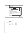
1
C60_2-019_818217_0806-e.p65
1
Manual
Electronic Identification Systems BIS
Processor BIS C-60_2
Profibus DP
Deutsch – bitte wenden!
2
No. 818 217 D/E • Edition 0806
Subject to modification.
Replaces edition 0608.
Balluff GmbH
Schurwaldstrasse 9
73765 Neuhausen a.d.F.
Germany
Phone +49 7158 173-0
Fax +49 7158 5010
[email protected]
www.balluff.com
C60_2-019_818217_0806-e.p65
3
Contents
Safety Considerations ................................................................................................................. 4
Introduction, BIS C Identification Systems .............................................................................. 5-7
BIS C-60_2 Processor, Basic knowledge for application ........................................................ 8/9
BUS interface PROFIBUS-DP .............................................................................................. 10-12
Compatibility with BIS C-6_2 processor .................................................................................. 13
Function Description:
Communication with the processor ................................................. 14
Input and Output Buffers ............................................................ 15/16
Output Buffer, configuration and explanation ............................. 17-20
Input Buffer, configuration and explanation ................................ 21-24
Parametering the BIS C-60_2 processor ................................... 25-28
Processing data carriers ............................................................ 29-35
Examples for protocol sequence .............................................. 36-53
Read/Write Times ............................................................................................................... 54/55
LED Display ............................................................................................................................. 56
BIS C-6002 BIS C-6022
Mounting Head / Processor ..............................................................................57 .................. 75
Opening the Processor .....................................................................................58 .................. 76
Installing the connection cables / Mounting the PG connection .............. 59/60
Interface information / Wiring Diagrams ..................................................... 61-68 ............. 77-80
Changing the EEPROM .....................................................................................69 .................. 81
Technical Data ............................................................................................. 70-72 ............. 82/83
Ordering Information: Ordering Code / Accessory .................................... 73/74 .................. 84
Appendix, ASCII Table ............................................................................................................. 85
english
4
Safety Considerations
Approved Operation
Series BIS C-60_2 processors along with the other BIS C system components comprise an
identification system and may only be used for this purpose in an industrial environment in
conformity with Class A of the EMC Law.
Installation and
Operation
Installation and operation should be carried out by trained personnel only. Unauthorized work
and improper use will void the warranty and liability.
When installing the processor, follow the chapters containing the wiring diagrams closely.
Special care is required when connecting the processor to external controllers, in particular
with respect to selection and polarity of the signals and power supply.
Only approved power supplies may be used for powering the processor. See chapter 'Technical Data' for details.
Use and Checking
Prevailing safety regulations must be adhered to when using the identification system. In particular, steps must be taken to ensure that a failure of or defect in the identification system
does not result in hazards to persons or equipment.
This includes maintaining the specified ambient conditions and regular testing for functionality
of the identification system including all its associated components.
4
Fault Conditions
Should there ever be indications that the identification system is not working properly, it
should be taken out of commission and secured from unauthorized use.
Scope
This manual applies to processors in the series BIS C-6002-019-...-03-... and
BIS C-6022-019-050-03-....
english
3
C60_2-019_818217_0806-e.p65
5
Introduction
BIS C Identification Systems
This manual is designed to assist the user in setting up the control program and installing and
starting up the components of the BIS C Identification System, and to assure rapid, troublefree operation.
Principles
The BIS C Identification Systems belongs in the category of
non-contact systems for reading and writing.
This dual function permits applications for not only transporting information in fixed-programmed Data carriers, but also for gathering and passing along up-to-date information as well.
☞
If 2 read/write heads are connected to a BIS C-60_2 processor, both heads can be operated
independently of each other. This means for example that you can read a Data carrier from one
head while writing to another Data carrier at the other head.
Some of the notable areas of application include
Applications
– for controlling material flow in production processes
(e.g. in model-specific processes),
for workpiece conveying in transfer lines,
in data gathering for quality assurance,
for gathering safety-related data,
– in tool coding and monitoring;
– in equipment organization;
– in storage systems for monitoring inventory movement;
– in transporting and conveying systems;
– in waste management for quantity-based fee assessment.
english
6
Introduction
BIS C Identification Systems
System Components
The main components of the BIS C Identification Systems are:
– Processor,
– Read/Write Heads and
– Data carriers
Configuration with
BIS C-6002
processor
PROFIBUS-DP
Processor BIS C-6002
Processor BIS C-6002
with
adapter
with
adapter
BIS C-670
BIS C-650
Processor BIS C-6002
with
read/
write head
Schematic
representation of an
Identification System
(example)
6
english
Read/write
head 2)
BIS C-65_
BIS C-35_
Read/write
heads 1)
BIS C-3_ _
Data carriers BIS C-1_ _-...
1
) BIS C-3_ _ series, except BIS C-350 and -352
2
) only BIS C-350 or -352
BIS C-3_ _
5
C60_2-019_818217_0806-e.p65
7
Introduction
BIS C Identification Systems
PROFIBUS-DP
Configuration with
BIS C-6022
processor
Processor BIS C-6022
Processor BIS C-6022
version -050
BIS C-3_ _
version -050
1)
BIS C-3_ _ Read/write heads
BIS C-3_ _
BIS C-3_ _
Data carriers BIS C-1_ _-...
Schematic
representation of an
identification system
(example)
1
) BIS C-3_ _ series, except BIS C-350 and -352
english
8
BIS C-60_2 Processor
Basic knowledge for application
Selecting System
Components
The BIS C-6002 processor has a plastic housing. Depending on the version, connections are
made either through a terminal strip, with the cable secured using a PG fitting, or via round
connectors. A single read/write head from BIS C-65_ series can be directly mounted to the
processor, which creates a compact unit. If the BIS C-650 adapter is attached instead of the
BIS C-65_ read/write head, two read/write heads may be cable connected. If the BIS C-670
adapter is attached, one read/write head may be cable connected.
The BIS C-6022 processor has a metal housing. Connection is made through round connectors. Two read/write heads can be cable connected to the BIS C-6022 processor.
Series BIS C-60_2 processors have in addition a digital input. The input has various functions
depending on the configuration (see Parametering).
Whether the compact version of the processor with integrated read/write head makes sense
or whether the external solution is preferred depends primarily on the spatial arrangement of
the components. There are no functional limitations. All read/write heads are suitable for both
static and dynamic reading. Distance and relative velocity are based on which Data carrier is
selected. Additional information on the read/write heads in series BIS C-65_ and series
BIS C-3_ _ including all the possible Data carrier/read-write head combinations can be found
in the manuals for the respective read/write heads.
The system components are electrically supplied by the processor. The Data carrier represents an free-standing unit and needs no line-carried power. It receives its energy from the
read/write head. The latter constantly sends out a carrier signal which supplies the code head
as soon as the required distance between the two is reached. The read/write operation takes
place during this phase. Reading and writing may be dynamic or static.
8
english
7
C60_2-019_818217_0806-e.p65
9
BIS C-60_2 Processor
Basic knowledge for application
Control Function
The processor writes data from the host system to the Data carrier or reads data from the
tag through the read/write head and prepares it for the host system. Host systems may
include:
– a host computer (e.g. industrial PC) or
– a programmable logic controller (PLC)
Data checking
When sending data between the read/write head and the Data carrier a procedure is required for recognizing whether the data were correctly read or written.
The processor is supplied with standard Balluff procedure of double reading and comparing. In addition to this procedure a second alternative is available: CRC_16 data checking.
Here a test code is written to the Data carrier, allowing data to be checked for validity at
any time or location.
Advantages of CRC_16
Data checking even during the non-active phase
(CT outside read/write head zone).
Shorter read times since each page is read only
once.
Advantages of double reading
No bytes on the data carrier need to be
reserved for storing a check code.
Shorter write times since no CRC needs to be
written.
Since both variations have their advantages depending on the application, the user is free
to select which method of data checking he wishes to use (see Parametering on 26).
☞
It is not permitted to operate the system using both check procedures!
english
10
BUS interface PROFIBUS-DP
PROFIBUS-DP
Communication between the BIS C-60_2 processor and the host system is via PROFIBUS-DP.
The PROFIBUS-DP system consists of the components:
– the bus master and
– the bus modules/slaves (here the BIS C-60_2 processor).
☞
Important hints for use with PLC:
In some control systems the PROFIBUS-DP data area is not synchronously transmitted with the
updating of the input/output content. If more than 2 bytes of data are sent, a mechanism must
be used which guarantees that the data in the PLC and the data in the BIS C are always identical!
1st alternative: Synchronous data transmission as a setting on the Master
In this method the bus Master ensures that all the data necessary for the respective Slave are
always sent contiguously. There is usually a special software function in the PLC which likewise
controls access between the PLC and bus Master so that data are always sent contiguously.
2nd alternative: Set 2nd bit header
Data exchange between PLC and BIS is controlled by the so-called bit header. This is always
the first byte of the respective read/write head in the data buffer. This bit header exists both in
the input range (data from BIS to the PLC) and in the output range (data from the PLC to the
BIS). lIf this bit header is also sent as the last byte, a comparison of these two bytes can be
used to guarantee the consistency of the transmitted data.
In this method the PLC cycle is unaffected nor is the bus access time changed. All that is
required is that a byte in the data buffer be used for the 2nd bit header instead of for user data.
This 2nd alternative is the Balluff recommended setting (factory default).
10
english
9
C60_2-019_818217_0806-e.p65
11
BUS interface PROFIBUS-DP
Unit's Master Data
For the correct parametering of the bus master as per type, a diskette, containing the unit’s
master data in the form of a GSD file is included with the BIS C-60_2 processor.
Station Address
The Processor BIS C-60_2 is delivered with the station address 126. This has to be set individually before using in a bus system. See information on 12.
Input/Output Buffer
An input buffer and an output buffer are used for the data exchange with the control system.
The size of these buffers has to be configured via the master.
☞
Parametering Bytes
User-Parameter Bytes
☞
The possible settings are entered in the GSD file (and Type file). A minimum of 4 and a maximum of 128 bytes can be accommodated. However, it must be an even number.
Besides, in the case of the BIS C-60_2 processor, there are 6 further bytes (User-Parameter
Bytes) which have to be set while parametering. The significance of the 6 bytes for parametering is described starting from 25.
The preset is stored in the GSD file.
11
english
12
BUS interface PROFIBUS-DP
Station Address
setting
The station address under which the unit is accessed on the bus can be assigned through the
slide switch S1. Each address shall be assigned only once.
The slide switch S1 is binary coded. The setting of the station address is carried out according
to the scheme shown in the table. Switch position: no = left, yes = right.
The address 85 is set in the following figure.
Slide switch S1
Station
Address
➪
7
6
5
4
3
2
1
26
25
24
23
22
21
20
1
no
no
no
no
no
no
yes
2
no
no
no
no
no
yes
no
3
no
no
no
no
no
yes
yes
0
no yes
not allowed
4
no
no
no
no
yes
no
no
5
no
no
no
no
yes
no
yes
yes
no
yes
no
yes
no
yes
123
yes
yes
yes
yes
no
yes
yes
124
yes
yes
yes
yes
yes
no
no
125
yes
yes
yes
yes
yes
no
yes
126
yes
yes
yes
yes
yes
yes
no
...
85
...
Slide switch S1
(with cover removed)
127
To open the cover of the processor, see
12
english
58 for BIS C-6002 or
not allowed
76 for BIS C-6022.
C60_2-019_818217_0806-e.p65
13
Compatibility with BIS C-6_2 processor
Setting compatibility
☞
Slide switch S1 is used to set compatibility with the BIS C-602 and BIS C-622 processors.
If the BIS C-60_2 processor is set to be compatible with the BIS C-602 or BIS C-622, all settings for data exchange must be made as described in the sections on parametering, function
description, protocol sequence and LED display in the user’s manual for the BIS C-6_2 processor! This user’s manual can be mailed on request, or you may download it from the Internet at
www.balluff.de.
➪
Slide switch S1
8
no yes
compatible with
yes
BIS C-6_2
no
BIS C-60_2
Key:
no = switch left
yes = switch right
In the illustration compatibility with the BIS C-6_2 is not set.
To open the cover of the BIS C-6002 processor, see
and for BIS C-6022 see 76.
58,
Slide switch S1
(with cover removed)
english
14
Function Description
Communication with the processor
Basic Procedure
Communication between the host system and the processor takes place using a fixed protocol sequence. Data integrity from the control to the processor and vice-versa is indicated by a
control bit. This bit is used to implement a handshake between the control and the processor.
Following is a simplified representation of the sequence of a job sent from the control to the
processor:
1. The control sends a command designator to the processor together with the associated
command parameters and sets a bit (AV bit). This bit indicates to the processor that the
transmitted data are valid and that the job is now beginning.
2. The processor takes the job and sets a bit (AA bit), which indicates this to the control.
3. If an additional exchange of data between the control and the processor is required to
carry out the job, each uses a bit (TI bit and TO bit) to indicate that the control / processor
is now ready for additional data exchange or has accepted the received data.
4. Once the processor has carried out the job correctly, it sets a bit (AE bit).
5. Once the control has accepted all the important data, it indicates this to the processor by
resetting the bit that was set at the beginning (AV bit).
6. The processor now in turn sets all the control bits that were set during the sequence
(AA bit, AE bit) and is ready for the next job.
Please see also
29...35 and the
examples on
36...53.
14
english
13
C60_2-019_818217_0806-e.p65
15
Function Description
Input and Output Buffers
Input and Output
Buffers
In order to transmit commands and data between the BIS C-60_2 and the host system, the
latter must prepare two fields. These two fields are:
– the output buffer
for the control commands which are sent to the BIS Identification System and
for the data to be written.
– the input buffer
for the data to be read and
for the designators and error codes which come from the BIS Identification System.
The possible setting values are stored in the GSD file.
The buffer size can be selected between 4 and 128 bytes in steps of 2 bytes. This must be
given by the master during parametering. The total buffer size is divided into 2 ranges:
Buffer range 1 for Read/Write Head 1; size is specified in paramter byte 6.
Buffer range 2 for Read/Write Head 2; size = total buffer size – buffer size of Read/Write
Head 1. See 16 for example.
☞
Please note the
basic procedure on
14 and 29...35
and the examples on
36...53.
pages
If a buffer size of less than 6 bytes (8 bytes with double bit header) is set for a read/write head, a
read/write request can be carried out without specifying the start address and the number of
bytes. Automatic reading for Codetag-Present (see 30) remains active. This permits fast
reading of small data quantities without placing an unnecessary load on the bus.
Buffer size – 1 = number of bytes read without double bit header;
Buffer size – 2 = number of bytes read with double bit header.
15
english
16
Function Description
Input and Output Buffers
Input and Output
Buffers
(continued)
Example: The 82 bytes for the total buffer need to be distributed. An input/output buffer of
46 bytes is assigned to Read/Write Head 1. This results in an input/output buffer of 36 bytes
for Read/Write Head 2.
Procedure: The buffer size for Read/Write Head 1 is set to 46 bytes. This means using the
parameter byte 6 to enter Hex value 2E (corresponds to 46 decimal), which corresponds to
binary 00101110.
PLC Organisation: The buffer range starts at input byte IB 32 and output byte OB 32.
Result:
Read/Write Head 1:
(R/W 1)
Read/Write Head 2:
(R/W 2)
☞
Subaddress 00
Input buffer
Output buffer
IB 32 and OB 32
IB 32 to IB 77
OB 32 to OB 77
Subaddress 00
Input buffer
Output buffer
IB 78 and OB 78
IB 78 to IB 113
OB 78 to OB 113
Note that these buffers can be in two different
sequences depending on the type of control.
The following description is based on sequence 1!
Please note the
basic procedure on
14 and 29...35
and the examples on
36...53.
pages
16
english
IB 0 / OB 0
PLC buffer
Buffer for R/W 1
Buffer for R/W 2
Sequence 1
Sequence 2
Subaddress 00
01
02
03
04
05
06
07
Subaddress 01
00
03
02
05
04
07
06
C60_2-019_818217_0806-e.p65
17
Function Description
Output buffer, configuration and explanation
Configuration of the
output buffer for one
(1) read/write head
The last byte can be arranged as a 2nd bit header through parametering (default).
Bit No.
7
6
5
4
3
2
1
0
Subaddress
00Hex = Bit Header
HD
GR
01Hex
CT
Command Designator
TI
or
02Hex
Start Address (Low Byte) or Program No.
or
Data
03Hex
Start Address (High Byte)
or
Data
04Hex
No. of Bytes (Low Byte)
or
Data
05Hex
No. of Bytes (High Byte)
or
Data
06Hex
Data
or
Data
...
Bit Name
Data
Last Byte
Description of
Output Buffer
AV
Data
Subaddress
2nd Bit Header (as above)
Bit
Meaning
Name
CT
00 Hex
Bit Header
Please note the
basic procedure on
14 and 29...35
and the examples on
36...53.
pages
Function Description
Data carrier type Select Data carrier type:
for Data carrier type:
0
32 Byte block size BIS C-1_ _-02, -03, -04, -05
1
64 Byte block size BIS C-1_ _-10, -11, -30
TI
Toggle-Bit In
HD
Head select
0
1
Shows during a read action that the controller is ready
for additional data.
for Head 1
for Head 2
Select Head 1.1
Select Head 2.1
Select Head 1.2
Select Head 2.2
(only in conjunction with Adapter 655)
(continued next )
english
18
Function Description
Output buffer, configuration and explanation
Description of
Output Buffer
(continued)
SubBit
Meaning
address
Name
GR
Ground state
00Hex
Bit Header
AV
Please note the
basic procedure on
14 and 29...35
and the examples on
36...53.
pages
18
english
Command
Function Description
Causes the BIS system to go to the ground state
for the respective read/write head.
Any pending command is cancelled.
Signals the identification system that a command
for the respective read/write head is present.
Subaddress
Meaning
01Hex
Command designator
No command present
00Hex
Read Data carrier
01Hex
Write to Data carrier
02Hex
Store program in the EEPROM for the Mixed Data Access
06HEX
function
Store the start address for the Auto-Read function in the
07 HEX
EEPROM
Copying from Head 1 to Head 2
11 HEX
Initialize the CRC_16 data check
12 HEX
Read for Mixed Data Access function
21HEX
(corresponding to the program stored in the EEPROM)
Write for Mixed Data Access function
22HEX
(corresponding to the program stored in the EEPROM)
Data
for writing to the Data carrier
Program data
for writing to the EEPROM.
or
or
(continued next )
Function Description
17
C60_2-019_818217_0806-e.p65
19
Function Description
Output buffer, configuration and explanation
Description of
Output Buffer
(continued)
Please note the
basic procedure on
14 and 29...35
and the examples on
36...53.
pages
Subaddress
Meaning
Function Description
02 Hex
Start address
(Low Byte)
or
Start address
(Low Byte)
or
Program No.
or
Program No.
or
or
Data
Program data
Address at which reading from or writing to the Data carrier
begins.
(The Low Byte includes the address range from 0 to 255).
Address for the Auto-Read function, starting at which the code
tag is to be read. The value is stored in the EEPROM. (The Low
Byte covers the address range from 0 to 255).
Number of the program to be stored in the EEPROM in
conjunction with command ID 06Hex for Mixed Data Access
function (values between 01Hex and 0AHex are allowed!).
Number of the program stored in the EEPROM for read or write
operations in conjunction with command ID 21Hex or 22 Hex for the
Mixed Data Access function.
for writing to the Data carrier
for writing to the EEPROM.
03 Hex
Byte
or
Start address
(High Byte)
Start address
(High Byte)
or
or
Data
Program data
Address for reading from or writing to the Data carrier (the High
is additionally used for the address range from 256 to 8,191).
Address for the Auto-Read function, starting at which the code
tag is to be read. The value is stored in the EEPROM (the High
Byte is also required for the address range from 256 to 8,191).
for writing to the Data carrier
for writing to the EEPROM.
(continued next )
english
20
Function Description
Output buffer, configuration and explanation
Description of
Output Buffer
(continued)
Subaddress
Meaning
Function Description
04Hex
No. of bytes
(Low Byte)
Data
Program data
Number of bytes to read or write beginning with the start address
(the Low Byte includes from 1 to 256 bytes).
for writing to the Data carrier
for writing to the EEPROM.
No. of bytes
(High Byte)
or
or
05Hex
or
Data
Number of bytes to read or write beginning with the start address
(the High Byte is additionally used for the range between 257 and
8,192 bytes).
for writing to the Data carrier
or
Program data
for writing to the EEPROM.
06Hex
or
Data
Program data
for writing to the Data carrier
for writing to the EEPROM.
...
Data
Program data
for writing to the Data carrier
for writing to the EEPROM.
or:
Last byte
Please note the
basic procedure on
14 and 29...35
and the examples on
36...53.
pages
20
english
or
or
2nd Bit header The data are valid if the 1st and 2nd bit header are identical.
Data
for writing to the Data carrier
Program data
for writing to the EEPROM.
19
C60_2-019_818217_0806-e.p65
21
Function Description
Input buffer, configuration and explanation
Configuration of the
input buffer for one
(1) read/write head
The last byte can be arranged as a 2nd bit header through parametering (default).
Bit No.
7
6
5
4
HF
TO
IN/KN
3
2
AF
AE
1
0
AA
CP
Subaddress
00Hex = Bit Header
BB
Error Code
01Hex
02Hex
Data
03Hex
Data
04Hex
Data
05Hex
Data
06Hex
Data
...
Please note the
basic procedure on
14 and 29...35
and the examples on
36...53.
pages
Bit Name
Data
Data
2nd Bit Header
(as above)
Last byte
Description of
Input Buffer
or
Subaddress
Bit
Meaning
Name
00Hex
BB
Bit Header HF
TO
or
Data
Function Description
Ready
The BIS Identification System is in the Ready state.
Head Error
Cable break from read/write head or
no read/write head connected.
Toggle-Bit Out
for read: BIS has new/additional data ready.
for write: BIS is ready to accept new/additional data.
(continued on next )
english
22
Function Description
Input buffer, configuration and explanation
Description of
Input Buffer
(continued)
Subaddress
Bit
Meaning
Name
Function Description
00Hex
(continued)
Bit Header IN/KN
Use the same bit in the bit header. Either IN or KN
may be displayed. Therefore select either Parameter
4th byte, bit 7 = 1 or Parameter 4th byte, bit 6 = 1.
(see 27)
IN
Input
If the parameter is 4th byte, bit 7 = 1 and 4th byte,
bit 6 = 0, this bit indicates the status of the input.
KN
Head No.
If the parameter is 4th byte, bit 6 = 1 and 4th byte,
bit 7 = 0, this bit indicates the selected head.
AF
Command Error The command was incorrectly processed or aborted.
AE
Command end
The command was finished without error.
AA
Command start The command was recognized and started.
CP
Codetag Present Data carrier present within the active zone of the
read/write head.
In addition to the CP bit, the output signal CT-Present is available. This allows
you to process the presence of a Data carrier directly as a hardware signal.
Please note the
basic procedure on
14 and 29...35
and the examples on
36...53.
pages
22
english
Subaddress
Meaning
01Hex
Error code
Function Description
Error number is entered if command was incorrectly processed
or aborted. Only valid with AF bit!
No error.
00Hex
Reading or writing not possible because no Data carrier is present
01Hex
in the active zone of a read/write head.
(continued on next )
21
C60_2-019_818217_0806-e.p65
23
Function Description
Input buffer, configuration and explanation
Description of
Input Buffer
(continued)
Please note the
basic procedure on
14 and 29...35
and the examples on
36...53.
pages
Subaddress
Meaning
01 Hex
Error code (continued)
Read error.
02Hex
Data carrier was removed from the active zone of the read/write
03Hex
head while it was being read.
Write error.
04Hex
Data carrier was removed from the active zone of the read/write
05Hex
head while it was being written.
AV bit is set but the command designator is missing or invalid.
07Hex
or Number of bytes is 00Hex .
Cable break to select read/write head, or head not connected.
09Hex
0CHex
The EEPROM cannot be read/programmed.
0DHex
Faulty communication with the Data carrier.
Note: Verify installation criteria or distance between data carrier
and read/write head.
The CRC of the read data does not coincide with the CRC of
0EHex
the Data carrier.
Contents of the 1st and 2nd bit header (1st and last bytes) of
0FHex
the output buffers are not identical (2nd bit header must be
served).
11Hex
Invoking a function that is not possible, since the processor is in
“compatible with BIS C-6_2” mode.
12Hex
Copying is not possible, since a command is already started
on Head 2.
Data
Data which was read from the Data carrier.
or:
Function Description
(continued on next )
english
24
Function Description
Input buffer, configuration and explanation
Description of
Input Buffer
(continued)
Subaddress
Meaning
Function Description
02Hex
Data
Data which was read from the Data carrier.
...
Data
Data which was read from the Data carrier.
2nd Bit header
The data are valid if the 1st and 2nd bit headers are in
agreement.
Data which was read from the Data carrier.
Last byte
or
Please note the
basic procedure on
14 and 29...35
and the examples on
36...53.
pages
24
english
Data
23
C60_2-019_818217_0806-e.p65
25
Function Description
Parametering the BIS C-60_2 processor
Parameters,
Overview
Please note the
basic procedure on
14 and 29...35
and the examples on
36...53.
pages
There are 6 user parameter bytes stored on the Profibus master that can be used to activate
and deactivate various functions. Setting is done directly by linking a device to the Profibus
master. The parameter default settings are stored in the GSD file.
– CRC_16 data check:
If this function is activated, the correctness of the read or written data is ensured by a
CRC_16 data check (see 9).
– Simultaneous data transmission for both read/write heads:
With simultaneous data transmission shorter read/write times can be achieved depending
on the amount of data to be read/written and the type of controller.
– Dynamic operation on read/write head 1 or 2:
If dynamic operation is parametered, a read/write job can be sent even though there is no
Data carrier in the active zone of the head. As soon as a Data carrier passes by the head,
the command is immediately carried out.
– "Auto-Read” for read/write head 1 or 2:
If this function is activated, the processor reads out the first (max. 31) bytes from the Data
carrier starting at a defined start address as soon as the tag enters the active zone of the
read/write head. The start address must first have been stored in the processor’s EEPROM
with the command ID 07Hex.
– 2nd bit header at end of in- and output buffer:
The 2nd bit header (factory setting) prevents data from being accepted by the bus as long
as it is not fully updated.
– Display state of the digital input in the bit header of the input buffer:
If this function is activated, the IN-bit displays the state of the digital input of the processor:
IN = 0 → digital input low; IN = 1 → digital input high
– Reset BIS C-60_2 processor through the digital input:
If this function is activated, the processor is reset when the digital input is set to high.
25
english
26
Function Description
Parametering, Parametering Bytes
Parametering Bytes
User-Parameter Bytes
For parametering all 6 bytes must always be transferred in Hex. Only the bits mentioned
may be changed. No guaranty will be given for the proper functioning of the
BIS C-60_2 if any of the other bits are changed.
The default values (factory setting) for the 6 bytes are:
1st byte
00
Binary 00000000
Hex
These are used for
configuration:
bit 5
2nd byte
80
10000000
bit 4
bit 5
3rd byte
00
00000000
4th byte
82
10000010
bit 6
bit 7 bit 2
bit 8
5th byte
00
00000000
6th byte
02
00000010
bit 4
bit 5
bit 8
bit 1...8
Having the following The bits which serve for parametering have the following functions:
functions:
1st byte, bit 5
Activate CRC_16 data checking
Bit state: 0 = no
1 = yes
☞
26
english
2nd byte, bit 5
Dynamic mode on read/write head 1
(for effects on read/write times, see
2nd byte, bit 4
Activate Auto-Read function starting at specified address after CTPresent for Head 1 (the number of bytes read depends on the selected
buffer size minus bit headers for Head 1)
4th byte, bit 8
Arrange a 2nd bit header at the end of the input and output buffers
54/55)
If this function is selected, then the minimum size of both buffers is 4 words (8 bytes) each.
Please note the basic procedure on
14 and 29...35 and the examples on pages
36...53.
C60_2-019_818217_0806-e.p65
27
Function Description
Parametering, Parametering Bytes
Parametering Bytes
User-Parameter Bytes
(continued)
4th byte, bit 7
0 = no
1 = yes
Display state of the digital input in the bit header of the input buffers:
Input is Low: "IN" in the bit header of the input buffers = 0.
Input is High: "IN" in the bit header of the input buffers = 1.
Important: „KN“ and „IN“ use the same bit in the bit header.
If the BIS C-655 adapter is connected for 2 x 2 heads, you must select 0 = no.
4th byte, bit 6
0 = no
1 = yes
Select read/write adapter 2 Head/4 Head connection
Select this setting if no more than 2 read/write heads can be connected.
Standard configuration.
Select this setting if the processor is being operated using the
BIS C-655 read head adapter and 2 x 2 heads.
Important: If 4th byte, bit 6 is set to 1 = yes, the setting 4th byte, bit 7 must be set to
0 = no.
4th byte, bit 2
0 = no
1 = yes
5th byte, bit 8
Bit state: 0 = no
1 = yes
Reset the BIS C-60_2 processor through the digital input:
Input is Low:
Do not reset.
Input is High:
Reset.
Activate simultaneous data transmission for both read/write heads
5th byte, bit 5
Dynamic mode on read/write head 2
(for effects on read/write times, see
5th byte, bit 4
Activate Auto-Read function for Head 2 starting at specified address
after CT-Present (the number of bytes read depends on the selected
buffer size minus bit headers for Head 2)
54/55)
6th byte, bit 1...8 No. of bytes in input and output buffer which shall be used for
read/write head 1, see example on 16
27
english
28
Function Description
Parametering, Parametering Bytes
Parametering Bytes
User-Parameter Bytes
(continued)
☞
28
english
The specification for the input and output buffer on the Master applies to both read/write
heads, i.e. this buffer must be divided for both heads. The specification is done in Hex
format and must be in a range between 02Hex and 80Hex (128 dec.).
If only one read/write head (Head 1) will be used, you may enter the same value here as for the
total buffer size. An entry of less than 2 bytes results in an undefined state.
Please note the basic procedure on
14 and 29...35 and the examples on pages
36...53.
C60_2-019_818217_0806-e.p65
29
Function Description
Processing data carriers
Reading and writing
To carry out a read or write job, the Data carrier must be located in the active zone of the read/
write head.
A read/write job has the following sequence (see examples on
38ff):
1. The host sends to the output buffer:
– the command designator to subaddress 01Hex,
– the start address for reading or writing to subaddress 02HEX/03HEX,
– the number of bytes for reading or writing to subaddress 04HEX/05HEX,
– the CT bit in the bit header according to the Data carrier type (block size),
– and sets the AV bit in the bit header to high.
2. The processor:
– takes the request (AA bit in the bit header of the input buffer to high),
– begins to transport the data;
read = from data carrier to input buffer,
write = from output buffer to data carrier.
Larger data quantities are sent in blocks
(block size with 2nd bit header = buffer size – 2),
block size without 2nd bit header = buffer size – 1).
The toggle bits in the two bit headers are used as a kind of handshaking between the
host and the BIS C-60_2 processor.
3. The processor has processed the command correctly (AE bit in the bit header of the input
buffer). If an error occurred during execution of the command, an error number will be
written to subaddress 01Hex of the input buffer and the AF bit in the bit header of the input
buffer will be set.
english
30
Function Description
Processing data carriers
Codetag Present
☞
As soon as the data carrier enters the active one of the read/write head, the processor indicates this by setting the CP bit (Codetag Present).
To accelerate the reading of small amounts of data, the ID system makes the first bytes of the
data carrier available in the input buffer of the respective read/write head as soon as the tag is
detected (30 bytes with 2nd bit header, 31 bites without 2nd bit header, or less if the buffer
size has been set smaller).
The data are only valid after the rising edge of the CP bit in the bit header of the input buffer.
They remain valid until the falling edge of the CP bit, or until the controller issues a new job.
Special
characteristics
To adjust the read/write functions to the numerous possible applications, a few unique features have been implemented that the user can select and set when parametering or programming the processor. These are as follows:
Auto-Read
If the Auto-Read function is activated, the data are read as soon as a data carrier is recognized. No command from the controller is required. Since there is an in- and output buffer for
each read/write head, the start address must be specified for each head using the command
designator 07Hex. The start addresses may be different. The number of bytes read is determined by the selected size of the input buffer, which is distributed over both heads when 2 are
used.
This distinguishes the Auto-Read function from the standard setting for automatic reading,
which always starts at Address 0 and includes a maximum number of 30 bytes with 2nd bit
header or 31 bytes without 2nd bit header (or les if the buffer size has been set smaller).
30
english
29
C60_2-019_818217_0806-e.p65
31
Function Description
Processing data carriers
Reading and writing
in dynamic mode
In normal operation a read/write job is rejected by the BIS C-60_2 processor by setting the AF
bit and an error number if there is no data carrier in the active zone of the read/write head. If
dynamic mode is configured, the processor accepts the read/write job and stores it. When a
data carrier is recognized, the stored job is carried out.
Reading and writing
with simultaneous
data transmission
Reading without simultaneous data transmission: In the case of a read job the processor first reads our all requested data from the data carrier after receiving the start address
and the desired number of bytes, and then sets the AE bit. Then the data read from the
data carrier are written to the input buffer. In the case of larger data amounts this is done in
blocks, controlled by the handshake with the toggle bits as described on 29.
Reading with simultaneous data transmission: In the case of a read job the processor
begins by transmitting the data into the input buffer as soon as the first 30 bytes (with 2nd
bit header, or 31 bytes without 2nd bit header, or less if the buffer size was set smaller)
have been read from the data carrier beginning with the start address, and indicates this
by inverting the TO bit. As soon as the controller inverts the TI bit, the processor sends the
data, which have in the meantime been read, to the input buffer. This is repeated until the
processor has read out all the desired data from the data carrier. Now the processor sets
the AE bit and outputs the remaining data on the input buffer.
Writing without simultaneous data transmission: In the case of a write job the processor waits until it has received all the data that need to be written from the controller. Only
then are the data written to the data carrier as described on 29.
Writing with simultaneous data transmission: In the case of a write job the processor
begins to write the data to the data carrier as soon as it has received the first data to be
written from the controller’s output buffer. Once all the data have been written to the data
carrier, the AE bit is set.
english
32
Function Description
Processing data carriers
Mixed Data Access
Small read/write programs can be stored in the BIS C-60_2 processor’s EEPROM.
The Mixed Data Access function is useful when the required information is stored on the
data carrier at various addresses. This function makes it possible to read out this “mixed”,
i.e. non-contiguously stored data from the data carrier in a single procedure and using just
one command.
Up to 10 programs with up to 25 instructions can be stored. Each program instruction contains a “start address” and a “number of bytes” specification. The amount of data for reading
may not exceed 2 kB.
Storing a program:
The command identifier 06Hex is used to send the read/write program to the BIS C-60_2 processor. One program per command can be stored. All 25 program records plus an additional
2 bytes with FFHexFFHex as a terminator must always be sent. This means a total of 104 bytes
of information per program must be sent (including the command identifier and program number).
☞
The individual program records must all be contiguous. They must be sent one after the other
and be terminated with 2 bytes FF HexFF Hex as a terminator. It is recommended that the remaining,
unused memory sector be filled with FFHexFF Hex.
If an address range is selected twice, the data will also be output twice.
32
english
31
C60_2-019_818217_0806-e.p65
33
Function Description
Processing data carriers
Mixed Data Access
(cont.)
The following shows the structure of a program:
Program structure
Subaddress
Value
Command designator
1. Program record
Program number
1st data record:
Start address Low Byte
Start address High Byte
Number of bytes Low Byte
Number of bytes High Byte
2nd data record:
...
25th data record:
Start address Low Byte
Start address High Byte
Number of bytes Low Byte
Number of bytes High Byte
Terminator
01Hex
06 Hex
02Hex
01Hex
Range
01Hex to 0AHex
03Hex
04Hex
05Hex
06Hex
03Hex
04Hex
05Hex
06Hex
FFHex FFHex
To store a second program, repeat this process.
The procedure for writing these settings to the EEPROM is described in the 10th example
48...50.
on
Replacing the EEPROM is described on
69 for BIS C-6002 and on
81 for BIS C-6022.
english
34
Function Description
Processing data carriers
Read from data
carrier, with program
Mixed Data Access
The command identifier 21Hex can be used to read out the program records stored in the program from the data carrier. The user must document exactly which data are to be read from
where and with what number of bytes for the respective program (see example 11 on 51).
Write to data carrier,
with program Mixed
Data Access
The command identifier 22Hex can be used to write the program records stored in the program to the data carrier. The user must document exactly which data are to be written from
where and with what number of bytes for the respective program (see example 12 on 52).
Copying from
Head 1 to Head 2
For a copy command there must be a data carrier in front of both read/write heads (even if
dynamic mode is configured). Simultaneous data transmission is used to read (even if simultaneous data transmission is not configured). The total process is controlled with the
bit header(s) for Head 1. The start address and number of bytes applies both to reading at
Head 1 and to writing at Head 2. The copy command is in principle the same as reading
with simultaneous data transmission. In addition, the data which are placed in the input
buffer are written at the same time to the data carrier at Head 2.
The AE bit is not set until the write procedure at Head 2 has finished successfully. If the
GR bit is set during a started copy command, both read/write heads are placed in the
base state and the pending job is aborted (see example 8 on 45).
34
english
33
C60_2-019_818217_0806-e.p65
35
Function Description
Processing data carriers
CRC initialization
To be able to use the CRC check, the data carrier must first be initialized with the command identifier 12Hex (see 36). The CRC initialization is used like a normal write job. The
latter is rejected (with an error message) if the processor recognizes that the data carrier
does not contain the correct CRC. Data carriers as shipped from the factory (all data are 0)
can immediately be programmed with a CRC check.
If CRC_16 data checking is activated, a special error message is output to the interface
whenever a CRC error is detected.
If the error message is not caused by a failed write request, it may be assumed that one
or more memory cells on the data carrier is defective. That data carrier must then be replaced.
If the CRC error is however due to a failed write request, you must reinitialize the data carrier in order to continue using it.
The checksum is written to the data carrier as a 2-byte wide datum. Two bytes per page
are 'lost', i.e., the page size becomes 30 bytes or 62 bytes depending on data carrier type
(setup of page size see 17). This means that the actual usable number of bytes is reduced:
Data carrier type
Usable bytes
128 bytes
=
120 bytes
256 bytes
=
240 bytes
511 bytes *)
=
450 bytes
1023 bytes *)
=
930 bytes
2047 bytes *)
=
1922 bytes
2048 bytes
=
1984 bytes
8192 bytes
=
7936 bytes
*) The last data carrier page for these EEPROMbased data carriers is not available.
english
36
Function Description
Examples for protocol sequence
Example No. 1
Initializing the Data carrier for the CRC_16 data checking
For configuring with
double bit header
and 8-byte buffer
size!
The processing of this command is similar to a write command. Start address and number
of bytes have to correspond to the maximum number of data to be used.
In this example the complete memory range of a Data carrier with 128 bytes shall be used
(BIS C-1_ _-03/L with 32 byte block size). Because 2 bytes are used for the CRC only
120 bytes can be used as data bytes, hence: start address = 0, number of bytes = 120.
Host:
BIS C-60_2 Identification System:
1.) Process subaddresses of the output buffer in the
order shown:
2.) Process subaddresses of the input buffer in the
order shown:
01Hex
Command designator 12Hex
02Hex
Start address 00 Hex
03Hex
Start address 00 Hex
04Hex
No. of bytes 78Hex
05Hex
No. of bytes 00Hex
00Hex /07Hex
Set AV-Bit, CT-Bit to 0
3.) Process subaddresses of the output buffer:
01...06 Hex
Enter first 6 bytes of data
00Hex /07Hex
Invert TI-Bit
00Hex /07Hex
4.) Process subaddresses of the output buffer:
01...06 Hex
...To be continued
until the complete
memory range is
written. See next .
36
english
01...06 Hex
Enter the second 6 data bytes
00Hex /07Hex
Invert TI-Bit
Copy first 6 data bytes
Process subaddress of the input buffer:
00Hex /07Hex
5.) Process subaddresses of the output buffer:
Set AA-Bit, invert TO-Bit
Invert TO-Bit
6.) Process subaddresses of the output buffer:
01...06 Hex
Copy second 6 data bytes
Process subaddress of the input buffer:
00Hex /07Hex
Invert TO-Bit
35
C60_2-019_818217_0806-e.p65
37
Function Description
Examples for protocol sequence
Example No. 1
(continued)
For configuring with
double bit header
and 8-byte buffer
size!
Host:
BIS C-60_2 Identification System:
7.) Process subaddresses of the output buffer:
01...06 Hex
Enter the remaining data byte
00Hex /07Hex
Invert TI-Bit
8.) Process subaddresses of the output buffer:
01...06 Hex
00Hex /07Hex
9.) Process subaddresses of the output buffer:
00Hex /07Hex
Reset AV-Bit
Copy the remaining data byte
Process subaddress of the input buffer:
Set AE-Bit
10.)Process subaddresses of the input buffer:
00Hex /07Hex
Reset AA-Bit and AE-Bit
english
38
Function Description
Examples for protocol sequence
Example No. 2
For configuring with
double bit header
and 8-byte buffer
size!
Read 17 bytes starting at data carrier address 10 (Data carrier type with 32 byte block size):
Host:
BIS C-60_2 Identification System:
1.) Process subaddresses of the output buffer in the
order shown:
00Hex /07Hex
Set AA-Bit
01...06 Hex
Enter first 6 bytes of data
03Hex
Start address High Byte 00Hex
00Hex /07Hex
Set AE-Bit
04Hex
05Hex
No. of bytes Low Byte 11Hex
No. of bytes High Byte 00Hex
00Hex /07Hex
CT-Bit to 0 (32 Byte block size),
set AV-Bit
3.) Process subaddresses of the input buffer:
01...06 Hex
Copy first 6 data bytes
Process subaddress of the output buffer:
00Hex /07Hex
01...06 Hex
Copy second 6 data bytes
Process subaddress of the output buffer:
00Hex /07Hex
Copy the remaining 5 data bytes
Process subaddress of the output buffer:
00Hex /07Hex
english
01...06 Hex
Enter the second 6 data bytes
00Hex /07Hex
Invert TO-Bit
6.) Process subaddresses of the input buffer:
01...05 Hex
00Hex /07Hex
Enter the remaining 5 data bytes
Invert TO-Bit
Invert TI-Bit
7.) Process subaddresses of the input buffer:
01...05 Hex
4.) Process subaddresses of the input buffer:
Invert TI-Bit
5.) Process subaddresses of the input buffer:
38
2.) Process subaddresses of the input buffer in the
order shown:
Command designator 01Hex
Start address Low Byte 0AHex
01Hex
02Hex
Reset AV-Bit
8.) Process subaddresses of the input buffer:
00Hex /07Hex
Reset AA-Bit and AE-Bit
37
C60_2-019_818217_0806-e.p65
39
Function Description
Examples for protocol sequence
Example No. 3
(like 2nd example
but with
simultaneous data
transmission)
For configuring with
double bit header
and 8-byte buffer
size!
Read 17 bytes starting at data carrier address 10, with simultaneous data transmission
(data carrier type with 32 byte block size):
While the read job is being carried out and as soon as the input buffer is filled, the first data
are sent. The AE bit is not set until the “Read” operation is completed by the processor.
The reply “Job End” = AE bit is reliably set no later than before the last data are sent. The
exact time depends on the requested data amount, the input buffer size and the timing of the
controller. This is indicated in the following by the note Set AE-Bit (in italics).
Host:
BIS C-60_2 Identification System:
1.) Process subaddresses of the output buffer in the
order shown:
2.) Process subaddresses of the input buffer in the
order shown:
01Hex
Command designator 01Hex
00Hex /07Hex
Set AA-Bit
02Hex
Start address Low Byte 0AHex
01...06 Hex
Enter first 6 bytes of data
03Hex
Start address High Byte 00Hex
00Hex /07Hex
Invert TO-Bit
04Hex
05Hex
No. of bytes Low Byte 11Hex
No. of bytes High Byte 00Hex
00Hex /07Hex
Set AE-Bit
00Hex /07Hex
CT-Bit to 0 (32 Byte block size),
set AV-Bit
3.) Process subaddresses of the input buffer:
01...06 Hex
Copy first 6 data bytes
Process subaddress of the output buffer:
00Hex /07Hex
Invert TI-Bit
Continued on next
4.) Process subaddresses of the input buffer:
01...06 Hex
Enter the second 6 data bytes
00Hex /07Hex
Invert TO-Bit
00Hex /07Hex
Set AE-Bit
.
english
40
Function Description
Examples for protocol sequence
Example No. 3
(continued)
(like 2nd example but
with simultaneous
data transmission)
For configuring with
double bit header
and 8-byte buffer
size!
40
english
Host:
BIS C-60_2 Identification System:
5.) Process subaddresses of the input buffer:
01...06 Hex
Copy second 6 data bytes
Process subaddress of the output buffer:
00Hex /07Hex
Invert TI-Bit
7.) Process subaddresses of the input buffer:
01...05 Hex
Copy the remaining 5 data bytes
Process subaddress of the output buffer:
00Hex /07Hex
Reset AV-Bit
6.) Process subaddresses of the input buffer:
01...05 Hex
Enter the remaining 5 data bytes
00Hex /07Hex
Invert TO-Bit
00Hex /07Hex
Set AE-Bit
8.) Process subaddresses of the input buffer:
00Hex /07Hex
Reset AA-Bit and AE-Bit
39
C60_2-019_818217_0806-e.p65
41
Function Description
Examples for protocol sequence
Example No. 4
Read 30 bytes starting at data carrier address 10 with read error
(data carrier type with 64 byte block size):
For configuring with
double bit header
and 8-byte buffer
size!
Host:
BIS C-60_2 Identification System:
1.) Process subaddresses of the output buffer in the
order shown:
2.) Process subaddresses of the input buffer in the
order shown:
If an error occurs right away:
01Hex
02Hex
Command designator 01Hex
Start address Low Byte 0AHex
00Hex/07Hex
Set AA-Bit
03Hex
Start address High Byte 00Hex
01Hex
Enter error number
04Hex
No. of bytes Low Byte 1EHex
00Hex/07Hex
Set AF-Bit
05Hex
00Hex /07Hex
No. of bytes High Byte 00Hex
Set CT-Bit to 1 (64 Byte block size),
set AV-Bit
3.) Process subaddress of the input buffer:
01Hex
Copy error number
4.) Process subaddresses of the input buffer:
00Hex/07Hex
Reset AA-Bit and AF-Bit
Process subaddress of the output buffer:
00Hex /07Hex
Reset AV-Bit
english
42
Function Description
Examples for protocol sequence
Example No. 5
(like 4th example
but with
simultaneous data
transmission)
Read 30 bytes starting at data carrier address 10, with read error and simultaneous data
transmission (data carrier type with 64 byte block size):
For configuring with
double bit header
and 8-byte buffer
size!
Host:
BIS C-60_2 Identification System:
1.) Process subaddresses of the output buffer in the
order shown:
2.) Process subaddresses of the input buffer in the
order shown:
If an error occurs right away:
If an error occurs, the AF bit is set instead of the AE-Bit, with a corresponding error number.
When the AF-BIT is set the job is interrupted and declared to be ended.
01Hex
02Hex
Command designator 01Hex
Start address Low Byte 0AHex
00Hex/07Hex
Set AA-Bit
03Hex
Start address High Byte 00Hex
01Hex
Enter error number
04Hex
No. of bytes Low Byte 1EHex
00Hex/07Hex
Set AF-Bit
05Hex
00Hex /07Hex
No. of bytes High Byte 00Hex
Set CT-Bit to 1 (64 Byte block size),
set AV-Bit
3.) Process subaddress of the input buffer:
01Hex
Copy error number
4.) Process subaddresses of the input buffer:
00Hex/07Hex
Reset AA-Bit and AF-Bit
Process subaddress of the output buffer:
00Hex /07Hex
☞
42
english
Reset AV-Bit
An error can also occur after the data have already been sent (see 6th example on the next ).
41
C60_2-019_818217_0806-e.p65
43
Function Description
Examples for protocol sequence
Example No. 6
(with simultaneous
data transmission)
For configuring with
double bit header
and 8-byte buffer
size!
Read 30 bytes starting at data carrier address 10, with read error and simultaneous data
transmission (data carrier type with 64 byte block size):
If an error occurs after data have started to be sent, the AF-Bit is set instead of the AE-Bit along
with the corresponding error number. The error message AF is dominant. It cannot be specified
which data are incorrect. When the AF-Bit is set the job is interrupted and declared to be ended.
Host:
BIS C-60_2 Identification System:
1.) Process subaddresses of the output buffer in the
order shown:
2.) Process subaddresses of the input buffer in the
order shown:
01Hex
02Hex
Command designator 01Hex
Start address Low Byte 0AHex
03Hex
Start address High Byte 00Hex
04Hex
No. of bytes Low Byte 1EHex
05Hex
00Hex /07Hex
No. of bytes High Byte 00Hex
Set CT-Bit to 1 (64 Byte block size),
set AV-Bit
3.) Process subaddress of the input buffer:
01...06 Hex
Copy first 6 data bytes
Process subaddress of the output buffer:
00Hex /07Hex
Invert TI-Bit
5.) Process subaddress of the input buffer:
01Hex
Copy error number
00 Hex/07 Hex
Set AA-Bit
01...06Hex
00 Hex/07 Hex
Enter the first 6 data bytes
Invert TO-Bit
4.) Process subaddresses of the input buffer:
If an error has occurred:
01Hex
Enter error number
00Hex/07Hex
Set AF-Bit
6.) Process subaddresses of the input buffer:
00Hex/07Hex
Reset AA-Bit and AF-Bit
Process subaddress of the output buffer:
00Hex /07Hex
Reset AV-Bit
english
44
Function Description
Examples for protocol sequence
Example No. 7
For configuring with
double bit header
and 8-byte buffer
size!
Write 16 bytes starting at data carrier address 20 (data carrier type with 32 byte block size):
Host:
BIS C-60_2 Identification System:
1.) Process subaddresses of the output buffer in the
order shown:
01Hex
Command designator 02Hex
02Hex /03Hex
04Hex /05Hex
Start address 14 Hex / 00Hex
No. of bytes 10Hex / 00 Hex
00Hex /07Hex
CT-Bit to 0 (32 Byte block size),
set AV-Bit
3.) Process subaddresses of the output buffer:
01...06 Hex
00Hex /07Hex
Enter the first 6 data bytes
Invert TI-Bit
2.) Process subaddresses of the input buffer in the
order shown:
00Hex /07Hex
4.) Process subaddresses of the output buffer:
01...06 Hex
01...06 Hex
Enter the second 6 data bytes
00Hex /07Hex
Invert TI-Bit
01...04 Hex
Enter the remaining 4 data bytes
00Hex /07Hex
Invert TI-Bit
01...06 Hex
00Hex /07Hex
44
english
Reset AV-Bit
Copy the second 6 data bytes
Process subaddress of the input buffer:
Invert TO-Bit
8.) Process subaddresses of the output buffer:
01...04 Hex
Copy the remaining 4 data bytes
Process subaddress of the input buffer:
00Hex /07Hex
9.) Process subaddresses of the output buffer:
Invert TO-Bit
6.) Process subaddresses of the output buffer:
00Hex /07Hex
7.) Process subaddresses of the output buffer:
Copy the first 6 data bytes
Process subaddress of the input buffer:
00Hex /07Hex
5.) Process subaddresses of the output buffer:
Set AA-Bit, invert TO-Bit
Set AE-Bit
10.)Process subaddresses of the input buffer:
00Hex /07Hex
Reset AA-Bit and AE-Bit
43
C60_2-019_818217_0806-e.p65
45
Function Description
Examples for protocol sequence
Example No. 8
Copy 17 bytes starting at data carrier address 10
(data carrier type with 32-byte block size):
For configuring with Data from the data carrier in front of Head 1 are read and written to the same memory lodouble bit header!
cation in the data carrier in front of Head 2. Data transmission can be started even while
the data carrier in front of Head 1 is being read. This is indicated by the TO bit in the input
buffer.
During data transmission ("toggling" of the TI bit / TO bit), and only then are the bytes read
written to the data carrier in front of Head 2. The AE bit is not set until the write process at
Head 2 has been successfully completed. Any errors at Head 2 are indicated by the AF bit
in the bit header for Head 1.
Host:
BIS C-60_2 Identification System:
1.) Process subaddresses of the output buffer in
the order shown:
2.) Process subaddresses of the output buffer in
the order shown:
01Hex
Command designator 11Hex
00Hex /07Hex
set AA-Bit
02Hex
Start address Low Byte 0AHex
Enter the first 6 data bytes
03Hex
04Hex
Start address High Byte 00Hex
No. of bytes Low Byte 11Hex
01...06 Hex
00Hex /07Hex
05Hex
No. of bytes High Byte 00Hex
00/07 Hex
CT-Bit to 0 (32 Byte block size),
set AV-Bit
3.) Process subaddresses of the input buffer:
01...06 Hex
Copy the first 6 data bytes
Process subaddresses of the output buffer:
00Hex /07Hex
Invert TI-Bit
Invert TO-Bit
4.) Process subaddresses of the input buffer:
01...06 Hex
00Hex /07Hex
Enter the second 6 data bytes
Invert TO-Bit
Continued on next .
english
46
Function Description
Examples for protocol sequence
Example No. 8
(continued)
5.) Process subaddresses of the input buffer:
01...06 Hex
Copy the second 6 data bytes
Process subaddresses of the input buffer:
For configuring with
double bit header!
00Hex /07Hex
01...05 Hex
Enter the remaining 5 data bytes
00Hex /07Hex
Invert TO-Bit
Invert TI-Bit
7.) Process subaddresses of the input buffer:
01...05 Hex
6.) Process subaddresses of the input buffer:
Copy the remaining 5 data bytes
8.) Process subaddresses of the input buffer:
00Hex /07Hex
Set AE-Bit
Process subaddresses of the output buffer:
00Hex /07Hex
Invert TI-Bit
9.) Process subaddresses of the output buffer:
00Hex /07Hex
46
english
Reset AV-Bit
10.)Process subaddresses of the input buffer:
00Hex /07Hex
Reset AA-Bit and AE-Bit
45
C60_2-019_818217_0806-e.p65
47
Function Description
Examples for protocol sequence
Example No. 9
Address assignment
for the Auto-Read
function
For configuring with
double bit header
and 8-byte buffer
size!
Programming start address 75 (data carrier type with 32 byte block size):
Host:
BIS C-60_2 Identification System:
1.) Process subaddresses of the output buffer in the
order shown:
2.) Process subaddresses of the input buffer:
00Hex /07Hex
01Hex
Command designator 06Hex
02Hex
03Hex
Start address Low Byte 488ex
Start address High Byte 008ex
00Hex /07Hex
CT-Bit to 0 (32 byte block size),
set AV-Bit
3.) Process subaddresses of the output buffer:
00Hex /07Hex
☞
4.) Process subaddresses of the input buffer:
00Hex /07Hex
Reset AV-Bit
Set AA-Bit and AE-Bit
Reset AA-Bit and AE-Bit
To ensure correct data output, use command identifier 07Hex for each distributed buffer Head 1
and/or Head 2.
If the Auto-Read function is not activated, the processor runs in standard mode and sends
starting with data carrier address 0 until the buffer is filled, but a maximum of 30 bytes for
double bit header or 31 bytes for a single bit header.
english
48
Function Description
Examples for protocol sequence
Example No. 10
Store Mixed Data
Access program
Storing a program for reading out 3 data records:
For configuring with
double bit header
and 8-byte buffer
size!
Total number of bytes exchanged in the operation:
1st data record
2nd data record
3rd data record
Start address
Start address
Start address
5
75
312
Number of bytes
Number of bytes
Number of bytes
7
3
17
27 bytes
All 104 bytes are written for the programming.
Host:
Host:
1.) Process subaddresses of the output buffer in the
order shown:
2.) Process subaddresses of the input buffer:
01Hex
02Hex
00Hex /07Hex
Command designator 06Hex
Program number 01Hex
CT-Bit to 0 or 1
(depending on block size),
set AV-Bit
3.) Process subaddresses of the output buffer:
01Hex
1st start address
02Hex
03Hex
04Hex
05Hex
Set AA-Bit, invert TO-Bit
4.) Process subaddresses of the input buffer:
00 Hex/07 Hex
Invert TO-Bit
(High Byte) 00 Hex
1st number of
bytes
2nd start address
06Hex
00Hex /07Hex
(Low Byte) 05 Hex
00 Hex/07 Hex
(Low Byte) 07 Hex
(High Byte) 00 Hex
(Low Byte) 4B Hex
(High Byte) 00 Hex
Invert TI-Bit
Continued on next .
48
english
47
C60_2-019_818217_0806-e.p65
49
Function Description
Examples for protocol sequence
Example No. 10
Store Mixed Data
Access program
(continued)
For configuring with
double bit header
and 8-byte buffer
size!
Host:
BIS C-60_2 Identification System:
5.) Process subaddresses of the output buffer:
6.) Process subaddresses of the input buffer:
01Hex
02Hex
03Hex
04Hex
2nd number of
bytes
3rd start address
(Low Byte) 03Hex
(High Byte) 00Hex
(Low Byte) 38Hex
(High Byte) 01Hex
05Hex
3rd number of
bytes
(Low Byte) 11Hex
06Hex
00Hex /07Hex
Invert TI-Bit
00 Hex/07 Hex
Invert TO-Bit
(High Byte) 00Hex
7.) Process subaddresses of the output buffer:
01Hex /02Hex
Terminator
FFHex /FFHex
03Hex /04Hex
(not used)
FFHex /FFHex
05Hex /06Hex
(not used)
FFHex /FFHex
00Hex /07Hex
Invert TI-Bit
8.) Process subaddresses of the input buffer:
00 Hex/07 Hex
Invert TO-Bit
Fill all unused start addresses and number of bytes with FFHex !
Continued on next .
english
50
Function Description
Examples for protocol sequence
Example No. 10
Store Mixed Data
Access program
(continued)
For configuring with
double bit header
and 8-byte buffer
size!
Host:
BIS C-60_2 Identification System:
9.) Process subaddresses of the output buffer:
10.)Process subaddresses of the input buffer:
01Hex /02Hex
(not used)
FFHex/FFHex
03Hex /04Hex
(not used)
FFHex/FFHex
05Hex /06Hex
00Hex /07Hex
(not used)
Invert TI-Bit
FFHex/FFHex
11.)Process subaddresses of the output buffer:
00Hex /07Hex
☞
Reset AV-Bit
00Hex /07Hex
Set AE-Bit
12.)Process subaddresses of the input buffer:
00Hex /07Hex
Reset AA-Bit and AE-Bit
We recommend that you carefully document which parameters are used for start addresses and
number of bytes for writing/reading the desired data records.
The data are sequenced in the exact order specified in the program.
50
english
49
C60_2-019_818217_0806-e.p65
51
Function Description
Examples for protocol sequence
Example No. 11
Use Mixed Data
Access program
For configuring with
double bit header
and 8-byte buffer
size!
Read data carrier using Program No. 1 (data carrier type with 32 byte block size):
Host:
BIS C-60_2 Identification System:
1.) Process subaddresses of the output buffer in the
order shown:
2.) Process subaddresses of the input buffer in the
order shown:
01Hex
Command designator 21Hex
00Hex /07Hex
Set AA-Bit
02Hex
00Hex /07Hex
Program number 01Hex
CT-Bit to 0 (32 byte block size),
set AV-Bit
01...06 Hex
Enter first 6 bytes of data
00Hex /07Hex
Set AE-Bit
3.) Process subaddresses of the input buffer:
4.) Process subaddresses of the output buffer:
01...06 Hex
01...06 Hex
00Hex /07Hex
Copy first 6 data bytes
Process subaddress of the output buffer:
00Hex /07Hex
Invert TO-Bit
Invert TI-Bit
... A total of 27 bytes of data are exchanged.
For the remainder of the procedure, see Example 2 on
☞
Enter the second 6 data bytes
38.
Dynamic mode is turned off while the Mixed Data Access program is being run.
english
52
Function Description
Examples for protocol sequence
Example No. 12
Use Mixed Data
Access program
For configuring with
double bit header
and 8-byte buffer
size!
Write data carrier using Program No. 1 (data carrier type with 32 byte block size):
Host:
BIS C-60_2 Identification System:
1.) Process subaddresses of the output buffer in
the order shown:
2.) Process subaddresses of the input buffer in the
order shown:
01Hex
Command designator 22Hex
02Hex
00Hex /07Hex
Program number 01Hex
CT-Bit to 0 (32 byte block size),
set AV-Bit
3.) Process subaddresses of the output buffer:
01...06 Hex
Enter first 6 bytes of data
00Hex /07Hex
Invert TI-Bit
00Hex /07Hex
4.) Process subaddresses of the output buffer:
01...06 Hex
00Hex /07Hex
52
english
Copy the first 6 data bytes
Process subaddress of the input buffer:
... A total of 27 bytes of data are exchanged.
For the remainder of the procedure, see Example 7 on
☞
Set AA-Bit, invert TO-Bit
Invert TO-Bit
44.
Dynamic mode is turned off while the Mixed Data Access program is being run.
51
C60_2-019_818217_0806-e.p65
53
Function Description
Examples for protocol sequence
Example No. 13
Put the relevant read/write head into ground state:
Both read/write heads can be independently set to the ground state.
Host:
BIS C-60_2 Identification System:
1.) Process subaddresses of the output buffer:
2.) Go to ground state;
Process subaddresses of the input buffer:
00Hex /07Hex
Set GR-Bit
00Hex /07Hex
3.) Process subaddresses of the output buffer:
00Hex /07Hex
00Hex /07Hex
Reset GR-Bit
Reset BB-Bit
4.) Process subaddresses of the input buffer:
Set BB-Bit
english
54
Read/Write Times
Read times from
Data carrier to
processor in
static mode
(parametering:
2nd byte, bit 5 = 0,
without CRC_16 data
check)
Write times from
processor to Data
carrier in static
mode
(parametering:
2nd byte, bit 5 = 0,
without CRC_16 data
check)
For double read and compare:
Data carrier with 32 byte blocks
Data carrier with 64 byte blocks
No. of bytes
Read time [ms]
No. of bytes
Read time [ms]
from 0 to 31
110
from 0 to 63
220
for each additional
32 bytes add
120
for each additional
64 bytes add
230
from 0 to 255
= 950
from 0 to 2047
= 7350
Including readback and compare:
Data carrier with 32 byte blocks
Data carrier with 64 byte blocks
No. of bytes
Write time [ms]
No. of bytes
Write time [ms]
from 0 to 31
110 + n * 10
from 0 to 63
220 + n * 10
for 32 bytes or more
y * 120 + n * 10
for 64 bytes or more
y * 230 + n * 10
n = number of contiguous bytes to write
y = number of blocks to be processed
Example: 17 bytes from address 187 have to be written. Data carrier with 32 bytes per block.
The blocks 5 and 6 will be processed since the start address 187 is in block 5 and the end
address 203 in block 6.
t = 2 * 120 + 17 * 10 = 410 ms
☞
54
english
The indicated times apply after the Data carrier has been recognized. If the Data carrier is not
yet recognized, an additional 45 ms for building the required energy field until the Data carrier is
recognized must be added.
53
C60_2-019_818217_0806-e.p65
55
Read/Write Times
Read times from
Data carrier to
processor in
dynamic mode
(parametering:
2nd byte, bit 5 = 1,
without CRC_16 data
check)
Read times within the 1st block for dual read and compare:
The indicated times apply after the Data carrier has been recognized. If the Data carrier is not
yet recognized, an additional 45 ms for building the required energy field until the Data carrier is
recognized must be added.
Data carrier with 32 byte blocks
Data carrier with 64 byte blocks
No. of bytes
Read time [ms]
No. of bytes
Read time [ms]
from 0 to 3
for each additional
byte add
from 0 to 31
14
from 0 to 3
for each additional
byte add
from 0 to 63
14
3.5
112
3.5
224
m = highest address to be read
Formula: t = (m + 1) * 3.5 ms
Example: Read 11 bytes starting at address 9, i.e. the highest address to be read is 19.
This corresponds to 70 ms.
english
56
LED Display
Function displays
on BIS C-60_2
The BIS C-60_2 uses the three side-mounted LED's to indicate important conditions of the
identification system.
Status
Ready / Bus active
LED
Meaning
red
Supply voltage OK; no hardware error,
however, bus not active.
Supply voltage / hardware OK,
bus active.
green
CT1 Present / operating
green
yellow
Data carrier read/write-ready at read/write head 1.
Read/write command at read/write head 1 in
process.
yellow flashes Cable break to read/write head or not connected.
off
No Data carrier in read/write range of
read/write head 1.
CT2 Present / operating
green
yellow
Data carrier read/write-ready at read/write head 2.
Read/write command at read/write head 2 in
process.
yellow flashes Cable break to read/write head or not connected.
off
No Data carrier in read/write range of
read/write head 2.
If all three LED's are synchronously flashing, it means a hardware error. Return the unit to the factory.
56
english
55
C60_2-019_818217_0806-e.p65
57
BIS C-6002
Mounting Head / Processor
Orientation of the
read/write head or
adapter
Depending on model, the processor is equipped with a read/write head or the adapter for
offset read/write heads. Both the read/write head and the adapter can be rotated by the user
by + or –90 deg. to the desired
Caution: wires inside!
position (see drawing). Be sure
that power is off first. Loosen
both screws (indicated with
arrows). Carefully pull the head
or adapter out towards the side
(direction of arrow, right drawing).
Caution: wires inside!
Reattach at the desired orientation and screw tight again.
Mounting the
BIS C-6002
processor
The processor is attached using
4 M4 screws.
english
58
BIS C-6002
Opening the Processor
Opening the
Processor
BIS C-6002
The BIS C-6002 processor must be opened to perform the following steps:
– Set PROFIBUS-DP address
– Activate/deactivate termination resistor
– Set/change compatibility mode
– Replace EEPROM
– Make electrical connections (supply voltage, in-/output,
PROFIBUS-DP connections).
Be sure that the unit is disconnected from power before
opening.
Remove the 4 screws on the BIS C-6002 and lift off the
cover.
Perform the desired action. To make the electrical connections, push the cables through the fittings. For additional
wiring details, see the following .
Mounting of the cover (4 screws),
max. permissible tightening torque: 0.15 Nm
Opening the processor
58
english
57
C60_2-019_818217_0806-e.p65
59
BIS C-6002-...-KL2
Installing the connection cables
Make connections
on the BIS C-6002
processor
The BIS C-6002 processor must be opened in order to make the connections for the supply
voltage, the digital input and the PROFIBUS connections (see 58).
First be sure that the unit is disconnected from power.
Remove the 4 screws on the BIS C-6002 and lift off the cover.
Guide the two PROFIBUS cables through the PG 11 fittings (see
.
mation on wiring, see the following
60). For additional infor-
Push the cable for supply voltage and for the digital input through the PG 9 fitting.
Close up the processor.
If the processor is equipped with an adapter:
–
–
BIS C-650:
BIS C-670:
Connect the read/write heads to terminals Head 1 and Head 2.
Connect the read/write head to terminal Head 1.
english
60
BIS C-6002-...-KL2
Mounting the PG Connection for PROFIBUS-DP
Connecting the
shield of the
PROFIBUS-DP cable
in the PG 11 housing
on the processor
BIS C-6002
After connecting the (field) bus leads to the termional block, make sure that the shield has
proper connection to the PG housing.
Screw socket
Inside O-ring
Cable clamp
Screw the
swivel nut
with a torque
of 4.17 Nm
60
english
ca. 3 - 4 mm
59
C60_2-019_818217_0806-e.p65
61
BIS C-6002-...-KL2
Interface Information / Wiring Diagrams
Remote bus cable
and interfaces for
PROFIBUS-DP
To insert BIS C-6002 processor into the serial PROFIBUS, terminals 1and 2 and 5 and 6 for
the PROFIBUS-DP interface are located on the terminal block ("incoming" and "outgoing").
Bus station BIS C-6002
Bus station
Bus station
Terminal
block
red
green
red
green
In case the processor is the last bus module in the chain, then only the incoming cable is connected. You can either use the connections 1 and 2 or 5 and 6.
The last bus module must terminate the bus with a resistor. In the case of the BIS C-6002, this
can be realized in two different ways:
S2
Terminating resistor
1. In the device
by closing the switch S2
(factory standard is open)
closed
open
active
passive
2. Outside the device in a plug. In this case the signals VP (terminal 4) and DGND (terminal 3)
should be brought out in order to connect the external resistor to the potential.
Note: In this case S2 has to be open!
61
english
62
BIS C-6002-...-KL2
Interface Information / Wiring Diagrams
Wiring diagram for
BIS C-6002
processor with
integrated read/write
head
7
6
5
4
3
2
1
DGND
A
B
VP
DGND
A
B
PROFIBUS-DP
13
12
11
10
9
8
+IN
–IN
+VSO
–VSO
01
02
INPUT
OUTPUT
01 = CT Present 1
02 = CT Present 2
Terminal
block
Protection
ground PE
PROFIBUS-DP
Terminal location and
designation
62
english
Supply voltage,
input/output
19
18
+VS
–VS
17
16
15
14
TxD
RxD
GND
POWER
RS 232
Terminal block connections
The ground connector should be connected to earth directly
or through a RC combination depending on the system (potential counterpoise).
When connecting the bus leads, make sure that the shield has
proper connection to the PG housing. Please note the assembling instructions on 60.
C60_2-019_818217_0806-e.p65
63
BIS C-6002-...-KL2
Interface Information / Wiring Diagrams
Wiring diagram
for BIS C-6002
processors with
adapter BIS C-650
7
6
5
4
3
2
1
DGND
A
B
VP
DGND
A
B
PROFIBUS-DP
13
12
11
10
9
8
+IN
–IN
+V SO
–VSO
01
02
INPUT
OUTPUT
01 = CT Present 1
02 = CT Present 2
19
Terminal
block
18
+VS
17
16
–VS
TxD
POWER
Protection
ground PE
Terminal location and
designation
PROFIBUS-DP
Supply voltage,
input/output
15
14
RxD
GND
RS 232
Terminal block connections
The ground connector should be connected to
earth directly or through a RC combination depending on the system (potential counterpoise).
When connecting the bus leads, make sure that the
shield has proper connection to the PG housing.
Please note the assembling instructions on 60.
63
english
64
BIS C-6002-...-KL2
Interface Information / Wiring Diagrams
Wiring diagram
for BIS C-6002
processors with
adapter BIS C-670
Terminal for read/write head (8 pin)
7
6
5
4
3
2
1
DGND
A
B
VP
DGND
A
B
PROFIBUS-DP
13
12
11
10
9
8
+IN
–IN
+VSO
–VSO
01
02
INPUT
OUTPUT
01 = CT Present 1
02 = CT Present 2
19
+VS
18
–VS
17
16
TxD
POWER
Terminal
block
Protection
ground PE
Terminal location and
designation
64
english
PROFIBUS-DP
Supply voltage, input/output
15
14
RxD
GND
RS 232
Terminal block connections
The ground connector should be connected to
earth directly or through a RC combination depending on the system (potential counterpoise).
When connecting the bus leads, make sure that the
shield has proper connection to the PG housing.
Please note the assembling instructions on 60.
C60_2-019_818217_0806-e.p65
65
BIS C-6002-...-ST11
Interface Information / Wiring Diagrams
Remote bus cable
for PROFIBUS-DP
To insert BIS C-6002-...-ST11 processor into the serial PROFIBUS-DP, there are the terminal
X2 for the PROFIBUS input and the terminal X3 for the PROFIBUS output.
Bus station BIS C-6002-...-ST11
Bus station
A
3 DGND
B
...
green
A 2
2A
red
DGND 3
B 4
4B
A
red
Connect shield
to connector
housing
Output
Bus station
VP 1
1 VP
green
B
Connect shield
to connector
housing
5-pin male
X2, input
Input
5-pin female
X3, output
In case the processor is the last bus module in the chain, then only the incoming cable is connected to X2.
The last bus module must terminate the bus with a resistor. In the case of the BIS C-602, this
can be realized in two different ways:
1. In the device by closing the switch S2
(factory standard is open)
Note: Output terminal must be closed
off with a screw cover in order to
maintain the enclosure rating.
S2
Terminating resistor
closed
open
active
passive
2. Outside the device in a connector to socket X3. In this case the signal VP (pin 1) and
DGND (pin 3) should be brought out in order to connect the external resistor to the potential. Note: In this case S2 has to be open!
65
english
66
BIS C-6002-...-ST11
Interface Information / Wiring Diagrams
Wiring diagram for
BIS C-6002-...-ST11
processor with
adapter BIS C-650
Connection for Read/Write Head 1
X1, supply voltage, digital input
Connection for
Read/Write Head 1
4
3
5
1
X2, PROFIBUSinput (male)
4
2
Pin
Function
1
+Vs
2
–IN
3
–Vs
4
+IN
5
n.c.
Pin
Function
X3, PROFIBUSoutput (female)
3
3
4
1
5
5
1
2
2
1
VP
2
A
3
DGND
4
B
5
n.c.
n.c. = do not connect
Terminal location
and designation
66
english
Supply
voltage,
digital input
Protection
ground PE
PROFIBUS-DP
The ground connector should be connected to
earth directly or through a RC combination
depending on the system (potential counterpoise).
When connecting the bus leads, make sure
that the shield has proper connection to connector housing.
C60_2-019_818217_0806-e.p65
67
BIS C-6002-...-ST11
Interface Information / Wiring Diagrams
Wiring diagram for
BIS C-6002-...-ST11
processor with
adapter BIS C-654
X1, supply voltage, digital input
Connection for
Read/Write Head
BIS C-355/...S92
4
3
Pin
Function
1
+Vs
5
X2, PROFIBUSinput (male)
4
–IN
3
–Vs
4
+IN
5
n.c.
Pin
Function
2
1
2
X3, PROFIBUSoutput (female)
3
3
4
1
5
5
2
1
1
2
VP
2
A
3
DGND
4
B
5
n.c.
n.c. = do not connect
Protection The BIS C-6002-654-03-ST11 processor may only be
ground PE operated in a compatible mode. This means switch S1/8
Terminal location
and designation
must be in the CN position (see 13). Please refer to the
manual for BIS C-6_2 for the parameter values and enabling
the "Select both heads" function and use the GSD file
C6x2.
Supply volt- PROFIBUS-DP
age, digital
input
The ground connector should be connected to earth directly or through
a RC combination depending on the system
.
(potential counterpoise).
When connecting the bus leads, make sure that the shield has proper connection to connector housing.
67
english
68
BIS C-6002-019-655-03-ST11
Interface Information / Wiring Diagrams
Wiring diagram
for BIS C-6002
processors with
adapter BIS C-655
(2 × 2 heads)
Connection for Read/Write Heads 1.1/1.2
Connection for
Read/Write Heads 2.1/2.2
X1, supply voltage, digital input
4
3
5
2
1
X2, PROFIBUSinput (male)
4
☞
Supply voltage,
digital input
PROFIBUS-DP
4
2
1
2
Function ground
FE
+Vs
–IN
3
–Vs
4
+IN
5
n.c.
Pin
Function
1
VP
2
A
3
DGND
4
B
5
n.c.
n.c. = do not connect
Terminal block connections
The ground connector should be connected to earth directly or through
a RC combination depending on the system (potential counterpoise).
When connecting the bus leads, make sure that the shield has proper
connection to connector housing.
68
3
5
1
Function
1
2
X3, PROFIBUSoutput (female)
3
5
Pin
english
11
10
9
8
BK
YE
GY
Head Select
C60_2-019_818217_0806-e.p65
69
BIS C-6002
Changing the EEPROM
Changing the
EEPROM in the
BIS C-6002
processor
To replace the EEPROM, open up the processor as described on
58.
Be sure before opening that the unit is disconnected from power..
To avoid damaging the EEPROM, please observe the requirements for handling electrostatically sensitive components.
The EEPROM is replaced by unplugging and
plugging back into the socket.
Location of the
EEPROM
english
70
BIS C-6002
Technical Data
70
Dimensions,
Weight
Housing
Dimensions with read/write head BIS C-65_
Dimensions with adapter BIS C-650
Weight
Plastic ABS
ca. 169 x 90 x 35 mm
ca. 185 x 90 x 35 mm
ca. 500 g
Operating
Conditions
Ambient temperature
0 °C to + 50 °C
Enclosure Rating
Enclosure rating
IP 65 (with read/write head)
Connections
BIS C-6002-...-KL2
Terminal block
Cable entry
Cable diameter
Cable entry
Cable diameter
19-pin
2 x PG 11 fittings (metal)
5 to 10 mm
1 x PG 9 fittings (metal)
4 to 8 mm
Conductor size
with ferrules
0.14 to 1 mm2
0.25 to 0.34 mm 2
Connections
BIS C-6002-...-ST11
Integral connector X1 for VS, IN
Integral connector X2 for PROFIBUS-DP Input
Integral connector X3 for PROFIBUS-DP Output
Electrical
Connections
Supply voltage VS, input
Ripple
Current draw
DC 24 V ± 20 %
≤ 10 %
≤ 400 mA
PROFIBUS-DP slave
electrically isolated
english
5-pin (male)
5-pin (male)
5-pin (female)
69
C60_2-019_818217_0806-e.p65
71
BIS C-6002
Technical Data
Digital Input (+IN, –IN)
Control voltage active
Control voltage inactive
Input current at 24 V
Delay time, typ.
Optocoupler isolated
4 V to 40 V
1.5 V to –40 V
11 mA
5 ms
with KL2 only: Control outputs CT Present 1 and 2
Output circuit PNP (current sourcing)
Operating voltage V SO (external) for output
Ripple
Output current
Voltage drop at 20 mA
Output resistance R A
Optocoupler isolated
Electrical
Connections
(continued)
DC 24 V ± 20 %
≤ 10 %
max. 20 mA
approx. 2.5 V
10 kΩ to –V SO
Service interface
RS 232
Read/Write Head
option for mounted adapter BIS C-650 *)
integrated, BIS C-65_ and following *);
2 x connectors 4-pin (male)
for all read/write heads BIS C-3_ _
with 4-pin connector (female),
except BIS C-350 and BIS C-352
1 x connector 8-pin (male)
for one of the read/write heads
BIS C-350 or BIS C-352
option for mounted adapter BIS C-670 *)
*) rotatable by 90 degrees
Function Displays
BIS operating messages:
Ready / Bus active
CT1 Present / operating
CT2 Present / operating
LED red / green
LED green / yellow
LED green / yellow
english
72
BIS C-6002
Technical Data
The CE-Mark is your assurance that our products are in conformance with the
EU Directive
2004/108/EC (EMC-Guideline)
and the EMC Law. Testing in our EMC Laboratory, which is accredited by the DATech for
Testing of Electromagnetic Compatibility, has confirmed that Balluff products meet the
EMC requirements of the Generic Standard
EN 61000-6-4 (Emission) and EN 61000-6-2 (Noise Immunity).
72
english
71
C60_2-019_818217_0806-e.p65
73
BIS C-6002
Ordering Information
Ordering Code
BIS C-6002-019-_ _ _-03-_ _ _
Balluff Identification System
Type C Read/Write System
Hardware Type
6002 = plastic housing, PROFIBUS-DP
Software-Type
019 = PROFIBUS-DP
Read/Write Head / Adapter
000 = no read/write head
651 = with read/write head Type 651 (with circular antenna on top)
652 = with read/write head Type 652 (with circular antenna on front)
653 = with read/write head Type 653 (with rod antenna)
650 = adapter with two connections for external read/write heads BIS C-3_ _
(except BIS C-350 and -352)
654 = adapter with one connection for external read/write heads BIS C-355/_ _S92
with cable BIS C-520-...
655 = adapter with 4 connections for external read/write heads BIS C-3_ _
(execpt BIS C-35_)
670 = adapter with one cable connection for an external read/write head
BIS C-350 or BIS C-352)
Interface
03 = bus versions
User Connection
KL2 = terminal block via 2 x PG 11 and 1 x PG 9 cable fittings
ST11 = Connector version X1, X2, X3 (2× male 5-pin, 1× female 5-pin)
english
74
BIS C-6002
Ordering Information
Accessory for ST11
Type
Connector
Protective cap
Termination
Protective cap
74
english
Ordering code
for X1
for X2
for X3
for X3
for X3
for Head 1, Head 2
BKS-S 79-00
BKS-S103-00
BKS-S105-00
BKS 12-CS-00
BKS-S105-R01
BES 12-SM-2
73
C60_2-019_818217_0806-e.p65
75
BIS C-6022
Mounting Processor
Mounting the
BIS C-6022
processor
The processor is mounted using 4 M4 screws.
Head 2 Head 1
ca. 15
M4
145
X2
160
X1
ca. 15
X3
X4
ca. 20
60
63
100
75
english
76
BIS C-6022
Opening the processor / Interface information
Opening the
BIS C-6022
processor
To set the PROFIBUS-DP address, activate or deactivate the internal termination resistor, set
the compatibility mode or to change the EEPROM, you must open up the BIS C-6022 processor.
Remove the 4 screws on the BIS C-6022 and lift off the cover. See the following
tional information.
BIS C-6022
interfaces
Head 2 Head 1
Connection for read/write head 2
Supply voltage,
X1
input,
output (ST10 only)
Connection locations
and names
76
for addi-
english
PROFIBUS-DP
X2
PROFIBUS-DP
X3
Service interface X4
Connection for read/write head 1
Be sure before
opening that the unit
is disconnected
from power.
Mounting of the cover
(4 screws),
max. permissible tightening
torque: 0.15 Nm
Protection ground PE
C60_2-019_818217_0806-e.p65
77
BIS C-6022
Interface Information / Wiring Diagrams
To insert BIS C-6022 processor into the serial PROFIBUS and to connect the supply voltage
and the digital input, the cables have to be connected to the terminals of the processor. For
more details regarding the wiring see the following . The read/write heads have to be connected to the to terminals Head 1 and Head 2.
PROFIBUS-DP
Ensure that the device is turned off.
Connect the "incoming" PROFIBUS cable to the PROFIBUS-Input. Connect the "outgoing"
PROFIBUS cable to the PROFIBUS-Output.
The last bus module must terminate the bus with a resistor. In the case of the BIS C-6022, this
can be realized in two different ways:
S2
Terminating resistor
1. In the device
by closing the switch S2
closed
active
(factory standard is open)
open
passive
The PROFIBUS-Output must
be closed off with a screw cover in order to maintain the enclosure rating.
2. Outside the device in a connector. In this case the signal VP and DGND should be brought
out in order to connect the external resistor to the potential.
Note: In this case the S2 switch has to be open!
No supply voltage is allowed on the PROFIBUS connections!
Connect cable for the supply voltage, the digital input, and the outputs to terminal X1.
77
english
78
BIS C-6022
Interface Information / Wiring Diagrams
Remote bus cable
for PROFIBUS-DP
BIS C-6022-...-ST10
To insert BIS C-6022 processor into the serial PROFIBUS-DP, there are the terminal X2 for the
PROFIBUS output and the terminal X3 for the PROFIBUS input.
Bus station
Bus station BIS C-6022-...-ST10
green
red
red
Connect shield
to connector
housing
Bus station
red
english
3 DGND
4B
B
78
1 VP
2A
A
...
12-pin female
X2, output
Input
Bus station BIS C-6022-...-ST14
green
Output
Connect shield
to connector
housing
12-pin female
X3, input
Output
BIS C-6022-...-ST14
Bus station
green
VP 1
A 2
DGND 3
B 4
Connect shield
to connector
housing
Bus station
green
A
red
B
Connect shield
to connector
housing
5-pin male
X2, input
5-pin female
X3, output
Input
C60_2-019_818217_0806-e.p65
79
BIS C-6022-...-ST10
Interface Information / Wiring Diagrams
Head 2 Head 1
Wiring diagram for
BIS C-6022-...-ST10
processor
X1, supply voltage, digital input, and
CT Present outputs
Pin
+Vs
CT Present 2
3
1
2
3
4
5
6
7
8
X1
Function
1
2
–Vs
4
+IN
5
CT Present 1
S1
X2, PROFIBUS output
X3, PROFIBUS input
Head 1
X2
Pin
Function
1
DGND
2
A
3
n.c.
Head 2
19 18 17 16 15 14 13 12 11 10 9 8 7 6 5 4 3 2 1
S2
X3
4
B
5
n.c.
6
VP
7
+24 V
8
GND
9
X4, Service interface
☞
X4
4
Protection
ground PE
10 ... 12
n.c.
Pin
Function
3
1
The ground connector should be connected to earth directly or through
a RC combination depending on the system (potential counterpoise).
When connecting the bus leads, make sure that the shield has proper
connection to connector housing.
n.c.
2
TxD
3
GND
4
RxD
2
1
n.c. =
do not connect!
79
english
80
BIS C-6022-...-ST14
Interface Information / Wiring Diagrams
Head 2 Head 1
Wiring diagram for
BIS C-6022-...-ST14
processor
X1, supply voltage, digital input
4
3
5
X1
1
2
3
4
5
6
7
8
2
1
Pin
Function
1
+Vs
2
–IN
3
–Vs
4
+IN
5
n.c.
Pin
Function
S1
X2, PROFIBUS
input (male)
Head 1
X2
X3, PROFIBUS
output (female)
Head 2
4
3
3
4
1
19 18 17 16 15 14 13 12 11 10 9 8 7 6 5 4 3 2 1
S2
5
X3
5
1
☞
Protection
ground PE
english
1
2
A
3
DGND
4
B
5
n.c.
Pin
Function
X4, Service interface
X4
The ground connector should be connected to earth directly or through
a RC combination depending on the system (potential counterpoise).
When connecting the bus leads, make sure that the shield has proper
connection to connector housing.
80
2
VP
2
4
3
1
1
2
n.c.
2
TxD
3
GND
4
RxD
n.c. =
do not connect!
C60_2-019_818217_0806-e.p65
81
BIS C-6022
Changing the EEPROM
Changing the
EEPROM in the
BIS C-6022
processor
To change the EEPROM, open the processor as described on
76.
Be sure before opening that the unit is
disconnected from power.
Head 2 Head 1
To avoid damaging the EEPROM, please
observe the requirements for handling
electrostatically sensitive components.
The EEPROM is replaced by unplugging
and plugging back into the socket.
X1
1
2
3
4
5
6
7
8
S1
Head 1
X2
Head 2
19 18 17 16 15 14 13 12 11 10 9 8 7 6 5 4 3 2 1
S2
X3
Location of the
EEPROM
X4
english
82
BIS C-6022
Technical Data
Dimensions, weight
Housing
Dimensions
Weight
Metal
190 x 120 x 60 mm
820 g
Operating conditions
Ambient temperature
0 °C to +60 °C
Enclosure
Protection class
IP 65 (when connected)
Connections
BIS C-6022-...-ST10
Integral connector X1 for VS, CT Present_, +IN
Round connector X2 / X3 for PROFIBUS-DP
Integral connector X4 for Service interface
5-pin (male)
12-pin (female)
4-pin (male)
Connections
BIS C-6022-...-ST14
Integral connector X1 for VS, +IN
Integral connector X2 for PROFIBUS-DP input
Integral connector X3 for PROFIBUS-DP output
Integral connector X4 for Service interface
5-pin (male)
5-pin (male)
5-pin (female)
4-pin (male)
Electrical
connections
Supply voltage VS
Ripple
Current draw
DC 24 V ± 20 %
≤ 10 %
≤ 400 mA
with ST10 only: Control outputs CT Present 1 and 2
Output circuit
Operating voltage VS for output
Ripple
Output current
Voltage drop at 20 mA
Output resistance RA
82
english
Optocoupler isolated
PNP (current sourcing)
DC 24 V ± 20 % via X1
≤ 10 %
max. 20 mA
approx. 2.5 V
10 kΩ to –VS
81
C60_2-019_818217_0806-e.p65
83
BIS C-6022
Technical Data
Electrical
Connections
(continued)
Digital input +IN
Control voltage active
Control voltage inactive
Input current at 24 V
Delay time, typ.
Optocoupler isolated
4 V to 40 V
1.5 V to –40 V
11 mA
5 ms
PROFIBUS-DP, Connector X2, X3
Head 1, Head 2, Read/Write Head
serial interface for PROFIBUS stations
via 2 x connectors for all
read/write heads BIS C-3_ _
with 4-pin connector (female),
excluding BIS C-350 and BIS C-352
RS 232
Service interface X4
Function displays
BIS operating messages:
Ready / Bus active
CT1 Present / operating
CT2 Present / operating
LED red / green
LED green / yellow
LED green / yellow
The CE-Mark is your assurance that our products are in conformance with the
EU Directive
2004/108/EC (EMC-Guideline)
and the EMC Law. Testing in our EMC Laboratory, which is accredited by the DATech for
Testing of Electromagnetic Compatibility, has confirmed that Balluff products meet the
EMC requirements of the Generic Standard
EN 61000-6-4 (Emission) and EN 61000-6-2 (Noise Immunity).
english
84
BIS C-6022
Ordering Information
Ordering code
BIS C-6022-019-050-03-ST_ _
Balluff Identification System
Type C Read/Write System
Hardware Type
6022 = metal housing, PROFIBUS-DP
Software Type
019 = PROFIBUS-DP
Version
050 = with two connections for external read/write heads BIS C-3_ _
(except BIS C-350 and -352)
Interface
03 = bus versions
User Connection
ST10 = Connector version X1, X2, X3, X4 (male: 1× 5-pin, 1× 4-pin, female: 2× 12-pin)
ST14 = Connector version X1, X2, X3, X4 (male: 2× 5-pin, 1× 4-pin, female: 1× 5-pin)
Accessory
(optional,
not included)
Type
Mating connector
Protective cap
Protective cap
Termination
84
english
for X1
for X2
for X3
for X4
for Head_, X4
Ordering code for ST10
Ordering code for ST14
BKS-S 79-00
BKS-S 86-00
BKS-S 86-00
BKS-S 10-3
BES 12-SM-2
115 475 for X2
BKS-S 79-00
BKS-S103-00
BKS-S105-00
BKS-S 10-3
BES 12-SM-2
BKS 12-CS-01 for X3
BKS-S105-R01 for X3
83
C60_2-019_818217_0806-e.p65
85
Appendix, ASCII Table
DeciControl
Hex
ASCII
mal
Code
0
00 Ctrl @ NUL
DeciControl
Hex
ASCII
mal
Code
22 16 Ctrl V SYN
DeciHex ASCII
mal
44 2C
,
DeciHex ASCII
mal
65 41
A
DeciHex ASCII
mal
86 56
V
DeciHex ASCII
mal
107 6B
k
1
01
Ctrl A
SOH
23
17
Ctrl W
ETB
45
2D
-
66
42
B
87
57
W
108
6C
l
2
02
Ctrl B
STX
24
18
Ctrl X
CAN
46
2E
.
67
43
C
88
58
X
109
6D
m
3
03
Ctrl C
ETX
25
19
Ctrl Y
EM
47
2F
/
68
44
D
89
59
Y
110
6E
n
4
04
Ctrl D
EOT
26
1A
Ctrl Z
SUB
48
30
0
69
45
E
90
5A
Z
111 6F
o
5
05
Ctrl E
ENQ
27
1B
Ctrl [
ESC
49
31
1
70
46
F
91
5B
[
112
70
p
6
06
Ctrl F
ACK
28
1C
Ctrl \
FS
50
32
2
71
47
G
92
5C
\
113
71
q
7
07
Ctrl G
BEL
29
1D
Ctrl ]
GS
51
33
3
72
48
H
93
5D
]
114
72
r
8
08
Ctrl H
BS
30
1E
Ctrl ^
RS
52
34
4
73
49
I
94
5E
^
115
73
s
Ctrl _
US
53
35
5
74
4A
J
95
5F
_
116
74
t
SP
54
36
6
75
4B
K
96
60
`
117
75
u
9
09
Ctrl I
HT
31
1F
10
0A
Ctrl J
LF
32
20
11
0B
Ctrl K
VT
33
21
!
55
37
7
76
4C
L
97
61
a
118
76
v
12
0C
Ctrl L
FF
34
22
"
56
38
8
77
4D
M
98
62
b
119
77
w
13
0D
Ctrl M
CR
35
23
#
57
39
9
78
4E
N
99
63
c
120
78
x
14
0E
Ctrl N
SO
36
24
$
58
3A
:
79
4F
O
100
64
d
121
79
y
15
0F
Ctrl O
SI
37
25
%
59
3B
;
80
50
P
101 65
e
122
7A
z
16
10
Ctrl P
DLE
38
26
&
60
3C
<
81
51
Q
102
66
f
123
7B
{
17
11
Ctrl Q
DC1
39
27
'
61
3D
=
82
52
R
103
67
g
124
7C
|
18
12
Ctrl R
DC2
40
28
(
62
3E
>
83
53
S
104
68
h
125
7D
}
19
13
Ctrl S
DC3
41
29
)
63
3F
?
84
54
T
105
69
i
126
7E
~
20
14
Ctrl T
DC4
42
2A
*
64
40
@
85
55
U
106
6A
j
127
7F
DEL
21
15
Ctrl U
NAK
43
2B
+
english
85