1
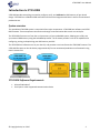
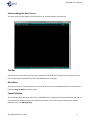
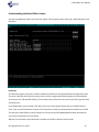
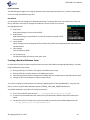
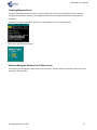
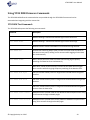
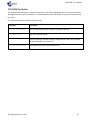
VTOS DDR™ User Manual March 25, 2015 VTOS DDR™ User Manual Table of Contents Introduction to VTOS DDR ................................................................................................................. 3 System overview ........................................................................................................................................3 VTOS DDR Software Requirements .............................................................................................................3 Using VTOS DDR Software ................................................................................................................. 4 Getting Started ..........................................................................................................................................4 Loading and Running VTOS DDR Firmware ..................................................................................................7 Configuring the DDR controller ...................................................................................................................8 Running DDR Tests .....................................................................................................................................8 Managing Logs ......................................................................................................................................... 11 Using Boards ............................................................................................................................................ 12 Creating Memory Parts............................................................................................................................. 16 Using the kScript Interpreter .................................................................................................................... 20 Tuning DDR .............................................................................................................................................. 21 Understanding the VTOS DDR Home Directory .......................................................................................... 21 Using VTOS DDR Firmware Commands ............................................................................................ 24 VTOS DDR Test Commands ....................................................................................................................... 24 VTOS DDR Test Suites ............................................................................................................................... 25 Understanding VTOS DDR Memory Tests ......................................................................................... 26 Memory Tests Quick Overview ................................................................................................................. 26 Running the SDRAM Tests ........................................................................................................................ 27 Measuring SDRAM Performance ............................................................................................................... 28 Configuring the SDRAM Tests ................................................................................................................... 29 Improvising RAM tests ............................................................................................................................. 30 Contact Information ........................................................................................................................ 40 About Kozio, Inc. ............................................................................................................................. 40 © Copyright Kozio, Inc. 2015 2 VTOS DDR™ User Manual Introduction to VTOS DDR VTOS DDR provides everything you need to configure, verify, and calibrate the DDR memory of your board design. VTOS DDR is a standalone DDR verification tool that also integrates with Kozio's vAccess for automated production test. System overview The standalone VTOS DDR system is comprised of two major components: VTOS DDR host software, and VTOS DDR firmware. These components communicate through a communication device such as a serial port. The VTOS DDR firmware runs from the on-chip memory of your embedded system, allowing you to fully test your external DDR memory using the embedded processor. The firmware provides a rich set of capabilities for configuring, testing, and optimizing your DDR memory and PHY. The VTOS DDR host software runs on your host PC, and provides a user interface to the VTOS DDR firmware. The VTOS DDR firmware can also be driven programmatically from an automated production test framework using Kozio’s vAccess DLL. VTOS DDR Software Requirements Microsoft Windows 7 Serial port or other supported communication device © Copyright Kozio, Inc. 2015 3 VTOS DDR™ User Manual Using VTOS DDR Software Getting Started Installing the Software VTOS DDR has a single installer that includes support for all supported architectures. To install the software, run the latest VTOS DDR installer. The installer creates program icons for launching the software under your Windows Start menu and places icons on your desktop for each supported architecture. For example, you will see an icon and start menu item for VTOS DDR (Sitara AM335). It also installs software resources and DUT firmware to a home directory in your User Profile directory. See Understanding the VTOS DDR Home Directory for further details. You can install support for multiple system architectures on the same machine. The installer creates resources that are specific to particular system architectures as necessary. Configuring the Software The first time you launch VTOS DDR, it will guide you through a number of steps to configure the software for your system. Installing a License VTOS DDR software requires a valid license for activation. A single license enables one instance of the software to be used on a specific host machine for a specific embedded system architecture. Contact [email protected] to obtain a license for your use. To install a license, launch an unlicensed instance of VTOS DDR. From the No License dialog, click OK to install a license. Use the file selection dialog to select your license file. VTOS DDR will install and validate the selected license. Selecting a Communication Device VTOS DDR software communicates with the VTOS DDR firmware using a communication device on your host machine. You must select which device on your host machine to use for this communication. VTOS DDR will prompt you to select a communication device when one has not previously been configured. From the Communication Device dialog, use the Up and Down arrow keys to highlight the device you wish to use from the list of available devices. Press Enter to select the device. © Copyright Kozio, Inc. 2015 4 VTOS DDR™ User Manual Tip: You can change the communication device using ‘Tools > Settings’. Configuring a Board VTOS DDR requires several parameters that differ by circuit board design. These parameters are stored in board configuration files. You must select a board configuration file that specifies these parameters for your circuit board. VTOS DDR will prompt you to select or create a board configuration file when one has not previously been configured. Using a Reference Board VTOS DDR includes board configuration files for popular reference boards. If your custom circuit board design is similar to one of these reference boards, you can select the reference board configuration file as a starting point, and tailor the board settings as necessary for your design. To use a reference board, select Open from the No Board File Configured dialog, and use the file browser to select a reference board file. Board configuration files come in two varieties: ‘register-based’ and ‘timing-based’. With timing-based files, the values for memory controller registers are derived from memory timing specifications. With register-based files, the values for memory controller registers are specified directly as numeric values. If you are starting with timing specifications from a memory data sheet as the basis for configuring the memory controller, select a timingbased file. If you are starting with a raw register dump, select a register-based file. Creating a New Board You can create a new board file rather than starting from a reference board. Select New from the No Board File Configured dialog, and use the board editor to specify the parameters for your board. See Using Boards. © Copyright Kozio, Inc. 2015 5 VTOS DDR™ User Manual Understanding the Main Screen The main screen has four regions: Title bar, Main menu, Console window, and Status bar. Title Bar The title bar runs across the top of the screen. It displays the product name and processor architecture on the left, and the version and build time of the VTOS DDR software on the right. Main Menu The main menu runs horizontally below the title bar. Main menu items are displayed with their hot key shown in bold. See Using the Menu for further details. Console Window The console window is below the main menu. VTOS DDR output is displayed in the console window. Tip: You can scroll the console window using the Up and Down arrow keys. You can also log the contents of the console window to a file. See Managing Logs. © Copyright Kozio, Inc. 2015 6 VTOS DDR™ User Manual Status Bar The status bar runs across the bottom of the screen. It is divided into four regions: Info, Board, Device, and Status. ● Info: Displays context-specific help information. ● Board: Displays the currently selected board configuration. ● Device: Displays the currently selected communication device. If there is a problem with the device, it will be highlighted in red. ● Status: Displays the state of the VTOS DDR software, Ready or Busy. Ready indicates that VTOS DDR is ready to process new commands. Busy indicates that VTOS DDR is running a command. Tip: You can interrupt the currently running command using Ctrl-C. Using the Menu Each item in the main menu has a “hot key” that is identified in bold. To select an item from the main menu, press Alt-<hot key>. For example, the hot key for the File menu item is F, and is identified with a bold font. To select the File menu item, press Alt-F. Once the menu has been activated by a hot key, you can navigate it using arrow keys. Use the Right and Left arrow keys to navigate across the main menu selections. Use the Up and Down arrow keys to select items from pull-down submenus. Use Enter to select the currently highlighted item from a pull-down submenu. Tip: As you navigate the menu, you can view a brief description of the currently highlighted item in the Info region of the Status bar. Loading and Running VTOS DDR Firmware The VTOS DDR software provides a user interface to the VTOS DDR firmware running on your embedded device. This firmware must be loaded and executed on your board using a boot loader, JTAG, or similar process. The VTOS DDR firmware images are installed in the VTOS DDR home directory on your host PC. See Understanding the VTOS DDR Home Directory for further details. © Copyright Kozio, Inc. 2015 7 VTOS DDR™ User Manual Please see the VTOS DDR Application Note for your system architecture for details on how to load and execute the VTOS DDR firmware image on your board. When the VTOS DDR firmware successfully boots, it prints the message “DUT Ready” in the VTOS DDR console window. The VTOS DDR firmware typically boots and is ready in under one second. Configuring the DDR controller You must configure the memory controller each time you boot the VTOS DDR firmware. VTOS DDR calculates the proper register values for the memory controller based on the data specified in your board configuration file, converting timing information into register values as necessary. To apply the register values to the controller hardware, select ‘Configure > Configure DDR controller’ from the VTOS DDR menu. The firmware will write the values to the hardware in the proper sequence to accomplish the specified configuration. Displaying register settings You can display the current values of the memory controller registers to the console. The values are given as a tabular display of register names and corresponding hexadecimal values. To display the values, select ‘Configure > Display DDR registers’. The VTOS DDR firmware reads the value of each register in the controller, and prints its value to the console. In some cases, memory controller registers are write-only, and consequently, the current value cannot be read. When a register is write-only, the last value written to the register is displayed. Exporting register settings You can export the current value of memory controller registers so that they can be used in other programs. The register values are converted into well-defined C data structures which can then be compiled into these programs. To export memory controller values, select ‘Configure > Export DDR configuration’. The exported values are displayed to the console. You can cut and paste these values into a text editor. You can also enable the console log to capture the exported values to the console log file. See Managing Logs. At the time of press, VTOS DDR can export data structures that are compatible with the U-Boot boot loader. You can use these data structures with U-Boot to ensure that U-Boot configures the system memory for your application with the same values that you have verified with VTOS DDR. Please see the VTOS DDR Application Note for your platform for further details. Running DDR Tests VTOS DDR provides a rich suite of memory tests that verify the design, layout, fabrication, and assembly of your DDR subsystem, including data and address bus tests, burst tests, noise tests, stress tests, and memory cell tests. © Copyright Kozio, Inc. 2015 8 VTOS DDR™ User Manual Note: Before testing DDR, you must configure the memory controller. See Configuring the DDR controller. You can run the DDR tests directly from the main menu. Test messages and pass/fail results are displayed to the console window. You capture log test results and console messages to log files for further analysis. See Managing Logs. Running Structural Tests To run a suite of structural tests, select ‘Test > Run structural tests’ from the main menu. The structural test suite checks for stuck-at faults that can arise from manufacturing defects such as faulty solder connections. It verifies that the data and address lines on the DDR bus are not stuck high or low. The structural test suite is comprised of the following tests: ● ● ● Data bus walking 0 Verifies each data bus signal can be driven low. Data bus walking 1 Verifies each data bus signal can be driven high. Address bus test Verifies each address line can be driven high and low. Running Noise Tests To run a suite of noise tests, select ‘Test > Run noise tests’ from the main menu. The noise test suite checks for data bus signal integrity problems such as crosstalk and reflection issues that can arise from design, layout, and manufacturing problems. The noise test suite is comprised of the following tests: ● ● ● Simultaneous Switching Output (SSO) Verifies successive reads and writes to the same memory word, holding one bit constant while toggling all other data bits simultaneously. Noise Verifies successive reads and writes while forcing high-frequency switching of all data bus lines simultaneously. Noise burst Similar to the noise test, but uses the CPU data cache to trigger burst transfers while forcing highfrequency switching of the data bus lines. Running Comprehensive Tests To run a suite of comprehensive tests, select ‘Test > Run comprehensive tests’ from the main menu. The comprehensive test suite checks for defective memory cells in addition to running all structural and noise tests. The comprehensive test includes the following in addition to all noise and structural tests. © Copyright Kozio, Inc. 2015 9 VTOS DDR™ User Manual ● ● ● Full byte Verifies memory cells in a range can be read and written using 8-bit accesses. Full word Verifies memory cells in a range can be read and written using 32-bit accesses. Full burst Verifies memory cells in a range can be read and written using burst accesses from the data cache. Tip: While VTOS DDR provides three separate tests to verify memory cells, in practice, the non-burst tests run much slower than the burst test. The global test setting are configured by default to run the non-burst tests over a small address range, and then run the burst test over the entire range. See Managing Test Settings. Managing Test Settings You can control the address ranges and bus width used by DDR tests by changing the global DDR test settings. To display the current settings in the console window, select ‘Test > Display test settings’ from the main menu. You can find descriptions of the DDR test settings in the table below: $sdram.bus.width Controls the access width used by the tests. Can be 8, 16, 32, or 64 bits, as supported by the hardware. $sdram.base64 Starting physical address of the memory test range. This is a 64-bit value. $sdram.len64 Length in bytes of the address range used for full burst tests. This is a 64bit value. $sdram.nonburst.len64 Length in bytes of the address range use for full non-burst tests. This is a 64-bit value. The DDR test settings are actually variables in the kScript scripting language. You can modify the values of these variables using the kScript command interpreter (‘Tools > Command’ or ‘Tools > Command Shell’). To assign a value to a setting, use the following syntax: value -> $variable © Copyright Kozio, Inc. 2015 10 VTOS DDR™ User Manual The assignment operator is comprised of two characters: Minus (-) and Greater (>). You must separate the value, assignment operator, and variable name with one or more spaces. To specify a constant value in hexadecimal, use the prefix ‘0x’ (e.g., 0xFF). Variables ending in ‘64’ are 64-bit values. To assign a 64-bit constant value to such a variable, use the ‘:64’ suffix (e.g., 0:64 specifies a 64-bit value of zero, 0xFF:64 specifies a 64-bit value of 255). Note: You must be connected to the VTOS DDR firmware to change DDR test settings. The settings are not persistent. You must apply them each time the VTOS DDR firmware reboots. Managing Logs You can capture VTOS DDR console text and test results to log files. These log files are stored in the ‘data’ subdirectory of the VTOS home directory. ● ● Console log Captures text written to the VTOS DDR console window. The log is a plain ASCII text file. Test log Captures results of DDR tests, including test name, parameters, and pass/fail result. The log is a commaseparated value (CSV) file that is compatible with third-party spreadsheet programs. To enable or disable these logs, select ‘Tools > Manage logs’. In the Enable/Disable Log Files dialog, use the Up and Down arrow keys to select the log you wish to manage. Use the Spacebar to toggle the state of the log. When the log is marked with an [x], it is enabled. Otherwise, it is disabled. © Copyright Kozio, Inc. 2015 11 VTOS DDR™ User Manual Using Boards VTOS DDR requires several parameters that differ by system architecture and circuit board design. These parameters are stored in board configuration files. You can load an existing board configuration, or create new configurations to tailor VTOS DDR to your custom circuit board. Board configuration files come in two varieties: ‘register-based’ and ‘timing-based’. With timing-based files, the values for memory controller registers are derived from memory timing specifications. With register-based files, the values for memory controller registers are specified directly as numeric values Load an Existing Board From the main menu, select ‘File > Open board’ to load settings from an existing board configuration file. Use the file browser to select the board file containing the desired settings. VTOS DDR updates the Board region in the Status bar with the name of the board you selected. The selected board is automatically loaded each time you launch VTOS DDR. Tip: VTOS DDR includes board configuration files for popular reference boards. If your circuit board is similar to a reference board, you can start by loading the reference board, and editing the settings as necessary for your board. Creating New Boards VTOS DDR provides a board configuration editor that enables you to create new board configurations and edit existing configurations. To launch the board editor, select ‘File > New board’ to create a new board, or ‘File > Edit current board’ to edit the currently selected board. © Copyright Kozio, Inc. 2015 12 VTOS DDR™ User Manual Understanding the Board Editor Screen The board configuration editor screen has five regions: Title bar, Board menu, Data entry, Data description, and Status bar. Data Entry The data entry region consists of a number of data entry fields that correspond with board configuration data. The cursor indicates which field is currently active. You can navigate the fields using either the Up and Down arrow keys or the Tab and Shift-Tab keys. To enter data into a field, move the cursor to the field, type the value, and press Enter. Some fields require you to choose a file. Move the cursor to the Browse button next to the field and press Enter. Then, use the file browser to select a file. The path to the file you selected will be entered into the field. The data entry fields differ by system architecture. Please see the VTOS DDR Application Note document for your system architecture for more details. Tip: You can enter Kozio script expressions into data entry fields as well as numeric values. © Copyright Kozio, Inc. 2015 13 VTOS DDR™ User Manual Data Description The data description region runs along the bottom of the screen above the Status bar. It contains a description of the currently selected data entry field. Board Menu Use the board menu to manage your edited board settings. To activate the menu, use the Alt-F key. Then, use the Up and Down arrow keys to navigate the submenu. Press the Enter key to choose the highlighted choice. ● ● ● ● ● Save board Save board settings to the current board file. Save board as Save board settings to a specified file. Use the file browser to specify the file name and folder. Import board Import settings from an existing board file. The data entry fields will be populated with values from the imported board. Clear settings Clear all data entry fields Exit to main menu Exit the board editor and return to the main menu. Creating a Board Initialization Script In some cases it may be necessary to perform actions on your board before configuring DDR memory. Possible board initialization steps include: ● ● ● ● Driving a GPIO pin to release a reset signal to the DDR memory chips Driving a GPIO pin to enable power to the DDR memory chips Communicating with a power management IC (PMIC) device to enable power to the DDR memory chips. Change the CPU core frequency to improve performance. You can use scripting to read and write any memory mapped registers of the embedded CPU. Using any text editor, create a script file under Windows directory %KOZIO_VTOS_DDR_HOME%\boards\user. Your board initialization script file must contain these items: ● ● ● Line 1 must of the file must be set to “// filetype=ddr-board_init_script” A custom command definition that contains all script commands needed to setup and initialize your board. The last line of the file installs your custom command for execution by the DDR configuration step. “=> my_board_init is ddr.board.init”. © Copyright Kozio, Inc. 2015 14 VTOS DDR™ User Manual Tip: There is a template file provided called %KOZIO_VTOS_DDR_HOME%\boards\user\board_init_script_template.ksc. An example board initialization script file for the AM437 GP EVM reference board is shown below. // filetype=ddr-board_init_script : am437_gp_evm.init // Print out information about what board script is running ." AM437 GP EVM board initialization" cr ." Driving GPIO5_7 high to enable VDDR_VTT" cr // Configure the pad for GPIO operation 0x00020007 0x44E10A5C write32 // Enable GPIO5 clocks 0x00000002 0x44DF8C98 write32 // Wait 100 microseconds 100 timer.delay.us // Enable GPIO5 module 0x00000000 0x48322130 write32 // Enable GPIO5_7, drive high 7 0x48322134 bitclear // clear bit in GPIO_OE 1 7 << 0x48322194 write32 // Write to SETDATAOUT ." Increasing MPU clock to 600 MHz" cr 600 mpu.clock.setup ." Board initialization complete" cr ; => am437_gp_evm.init is ddr.board.init After creating your board initialization script, you must edit your board file using the VTOS DDR board editor, and select the file using the “Board initialization file” selection dialog. © Copyright Kozio, Inc. 2015 15 VTOS DDR™ User Manual Creating Memory Parts Using the VTOS DDR memory part editor, you can create new memory part configuration files for use with timing-based board files. Memory part configuration files contain timing information from memory part datasheets. To launch the memory part editor, select ‘File > New memory part’ from the main menu. Next, select the memory part type. Understanding the Memory Part Editor Screen The memory part configuration editor screen has five regions: Title bar, Memory part menu, Data entry, Data description, and Status bar. © Copyright Kozio, Inc. 2015 16 VTOS DDR™ User Manual Data Entry The data entry region consists of a number of data entry fields that correspond with memory part data sheet timing parameters. The cursor indicates which field is currently active. You can navigate the fields using either the Up and Down arrow keys or the Tab and Shift-Tab keys. To enter data into a field, move the cursor to the field, type the value, and press Enter. Tip: You can enter Kozio script expressions into data entry fields as well as numeric values. The data entry region is split into 3 data field types. The DDR type and geometry fields are listed as a single column at the top of the Data entry region. © Copyright Kozio, Inc. 2015 17 VTOS DDR™ User Manual DDR timing parameters that are entered as an integer number of DDR clock cycles are listed in the first column with the heading “Timing Parameter in clocks”. DDR timing parameters that are entered as an integer number of picoseconds are listed in the second column with the heading “Timing Parameters in picoseconds”. © Copyright Kozio, Inc. 2015 18 VTOS DDR™ User Manual Some DDR timing parameters appear in both columns. In this case VTOS DDR automatically selects the value that results in the most conservative timing. For example, a datasheet for a DDR3 memory part may specify the minimum tWTR timing parameter as “greater of 4CK or 7.5 ns”. In this case, the tWTR field in the first column is set to 4, and the tWTR field in the second column is set to 7500. For a given parameter if the memory vendor datasheet only provides timing information in clocks, set the corresponding picosecond value in the second column to 0. If the memory vendor datasheet only provides timing information in nanoseconds/picoseconds, set the corresponding clock value in the first column to 0. Data Description The data description region runs along the bottom of the screen above the Status bar. It contains a description of the currently selected data entry field, as well as the name of the current memory part file. Memory Part Menu Use the memory part menu to manage your edited memory part settings. To activate the menu, use the Alt-F key. Then, use the Up and Down arrow keys to navigate the submenu. Press the Enter key to choose the highlighted choice. ● ● ● ● ● Save memory part Save memory part settings to the current file. Save memory part as Save memory part settings to a specified file. Use the file browser to specify the file name and folder. Import memory part Import settings from an existing memory part file. The data entry fields will be populated with values from the imported memory part. Clear settings Clear all data entry fields Exit to main menu Exit the memory part editor and return to the main menu © Copyright Kozio, Inc. 2015 19 VTOS DDR™ User Manual Using the kScript Interpreter The kScript scripting language is a powerful programming language that allows you to automate and extend the functionality of VTOS DDR. Please see the VTOS DDR Command Shell document for more details about kScript. You can run kScript commands from the VTOS DDR user interface, or exit to a command shell to interact with the kScript interpreter directly. You can also load kScript script files that are stored on your host file system. Running kScript Commands To run kScript commands from the user interface, select ‘Tools > Command’ from the main menu. Type the commands that you wish to run into the command text box, separated by spaces. Press the Enter key to run the commands. Loading Scripts You can load kScript files that are stored on your host file system. To load a kScript file, select ‘Tools > Load script’. Use the file browser to select the script you want to load. When you load a kScript file, it is interpreted by the kScript interpreter immediately. Your kScript files can create new commands, and also run existing commands. Your kScripts can define complex control flows using the rich constructs available in the kScript language. Invoking the Command Shell To exit the VTOS DDR user interface and enter the kScript command shell, select ‘Tools > Command shell’ from the main menu. The command shell prints a prompt to indicate that it is ready to accept commands. You can type commands directly into the console. You can also drag and drop kScript files onto the console. To return to the VTOS DDR user interface, type DDRMENU at the command prompt and press Enter. © Copyright Kozio, Inc. 2015 20 VTOS DDR™ User Manual Tuning DDR You can use VTOS DDR to tune the settings of your memory controller and DDR PHY for best operation with your circuit board. The tuning process differs by system architecture. The tuning process is performed from the command shell using script files included with VTOS DDR. Please see the VTOS DDR Application Note for further details. Understanding the VTOS DDR Home Directory The installer creates a VTOS DDR home directory in your User profile directory. The home directory contains software and firmware resources for the VTOS DDR system. The location of this directory is stored in the %KOZIO_VTOS_DDR_HOME% environment variable. Firmware Images VTOS DDR firmware images are stored in the VTOS_DDR directory. VTOS DDR firmware images adhere to the following naming convention: vtos.<system-architecture>_ddr.elf ELF object file. Compatible with a wide variety of loaders, including many JTAG-based loaders vtos.<system-architecture>_ddr.img U-Boot compatible vtos.<system-architecture>_ddr.srec Motorola S-Record vtos.<system-architecture>_ddr.bin Raw binary © Copyright Kozio, Inc. 2015 21 VTOS DDR™ User Manual Board Folder Board configuration files are stored in the ‘board’ folder. This folder contains a ‘user’ subfolder along with subfolders for various system architectures. The ‘user’ folder is a container for your custom board configuration files. You should store your custom board configuration files under the ‘user’ folder to ensure that they are preserved by future updates of the VTOS DDR software. Board configuration files come in two varieties: ‘register-based’ and ‘timing-based’. With timing-based files, the values for memory controller registers are derived from memory timing specifications. With register-based files, the values for memory controller registers are specified directly as numeric values. Board configuration files adhere to the following naming convention: <board-name>_timing_based.ksc Timing-based board configuration file <board-name>_register_based.ksc Register-based board configuration file Board configuration files are plain ASCII text. Their contents differs by system architecture. Please see the VTOS DDR Application Note document for your system architecture for more details. Memory_parts Folder Memory part configuration files are stored in the ‘memory_parts’ folder. This folder contains a ‘user’ subfolder along with subfolders for various memory vendors. The ‘user’ folder is a container for your custom memory part configuration files. You should store your custom memory part configuration files under the ‘user’ folder to ensure that they are preserved by future updates of the VTOS DDR software. Memory part configuration files adhere to the following naming convention: <vendor>_<ddr-type>_<part-number>-<speed-grade>.ksc Memory part configuration files are plain ASCII text. They contain data sheet timing specifications for particular memory parts. Scripts Folder kScript files are stored in the ‘scripts’ folder. This folder contains two subfolders: ‘kozio’ and ‘user’. The ‘kozio’ folder contains script files supplied by Kozio. The ‘user’ folder is a container for your custom scripts. You should store your custom scripts under the ‘user’ folder to ensure that they are preserved by future updates of the VTOS DDR software. kScript files are plain ASCII text. The kScript scripting language is a powerful programming language that allows you to automate and extend the functionality of VTOS DDR. Please contact [email protected] for requests and additional details. © Copyright Kozio, Inc. 2015 22 VTOS DDR™ User Manual Data Folder The data folder contains log files generated by VTOS DDR. There are three types of log files: debug logs, console logs, and test logs. When multiple instance of VTOS DDR are running, each instance creates its own set of log files. Log files adhere to the following naming convention: debug.instance<n>.log Debug log for instance n console.instance<n>.log Console log for instance n test.instance<n>.csv Test log for instance n ● ● ● Debug logs Always created by VTOS DDR. Debug logs are plain ASCII text. They contain information to help troubleshoot problems with the VTOS DDR software. Console logs Only created when enabled. See Managing Logs. Console logs are plain ASCII text. They contain a transcript of messages written to the VTOS DDR console window. Test logs Only created when enabled. See Managing Logs. Test logs are comma-separated value (CSV) files. They contain a history of test runs, including test algorithm name, test parameters, and pass/fail result. Etc Folder The etc folder contains miscellaneous program resources, including INI files that control VTOS DDR program settings. The INI file is managed by the program, and should not be edited by users. The etc folder also stores example JTAG debugger configuration files for popular JTAG devices. You can use these files to initialize your debugger for use with VTOS DDR. Please see the VTOS DDR Application Note for further details. © Copyright Kozio, Inc. 2015 23 VTOS DDR™ User Manual Using VTOS DDR Firmware Commands The VTOS DDR API defines the commands that are provided through the VTOS DDR firmware and can be executed when integrating with the vAccess DLL. VTOS DDR Test Commands The VTOS DDR API exposes the following test commands: Command Description test.sdram.walk0 Data bus walking 0. Verifies each data bus signal can be driven low. test.sdram.walk1 Data bus walking 1. Verifies each data bus signal can be driven high. test.sdram.address Address bus test. Verifies each address line can be driven high and low. test.sdram.sso Simultaneous Switching Output (SSO). Verifies successive reads and writes to the same memory word, holding one bit constant while toggling all other data bits simultaneously. test.sdram.noise Noise. Verifies successive reads and writes while forcing high-frequency switching of all data bus lines simultaneously. test.sdram.noise.burst Noise burst. Similar to the noise test, but uses the CPU data cache to trigger burst transfers while forcing high-frequency switching of the data bus lines. test.sdram.full.byte Full byte. Verifies memory cells in a range can be read and written using 8-bit accesses. test.sdram.full.word Full word. Verifies memory cells in a range can be read and written using 32-bit accesses. test.sdram.full.burst Full burst. Verifies memory cells in a range can be read and written using burst accesses from the data cache. perf.sdram.cache.read32 DDR performance (cached reads 32-bit). Measures DDR read performance using 32-bit accesses through cacheable pages. perf.sdram.cache.write32 DDR performance (cached writes 32-bit). Measures SDRAM write performance using 32-bit accesses through cacheable pages. © Copyright Kozio, Inc. 2015 24 VTOS DDR™ User Manual VTOS DDR Test Suites The VTOS DDR API also exposes a number of test suites. A test suite is grouping of one or more test commands. Although these test suites are provided, it is recommended that your test executive use test commands and not test suites. The VTOS DDR API exposes the following test suites: Command Description test.ddr.structural Data bus walking 0, data bus walking 1, and address bus test. test.ddr.noise SSO, noise, and noise burst. test.ddr.comprehensive Data bus walking 0, data bus walking 1, address bus test, SSO, noise, full byte, full word, full burst, and noise burst. test.ddr.performance Cached reads 32-bit and cached writes 32-bit. © Copyright Kozio, Inc. 2015 25 VTOS DDR™ User Manual Understanding VTOS DDR Memory Tests VTOS DDR firmware provides several preprogrammed tests that use the CPU to exercise your SDRAM devices. These tests exercise the data and address busses to SDRAM, and verify correct operation of the memory controller. The tests also verify that SDRAM devices can store data without data corruption. A synopsis of each test is given below: Memory Tests Quick Overview TEST.SDRAM.WALK0 - Tests that each bit on the data bus to SDRAM can be set to logical 0. The CPU performs writes to a single address in SDRAM using a rotating 0 data pattern. The CPU verifies each write by reading back the address and comparing its data to the data that was written. The CPU data cache is disabled for the duration of the test. See Creating Data Bus Tests for a detailed description of the underlying test algorithm. TEST.SDRAM.WALK1 - Tests that each bit on the data bus to SDRAM can be set to logical 1. The CPU performs writes to a single address in SDRAM using a rotating 1 data pattern. The CPU verifies each write by reading back the address and comparing its data to the data that was written. The CPU data cache is disabled for the duration of the test. See Creating Data Bus Tests for a detailed description of the underlying test algorithm. TEST.SDRAM.ADDRESS - Tests that each address line to SDRAM can be set high and low, and that no address lines are shorted. The CPU performs writes to a series of address offsets in SDRAM. The address offsets are chosen in a manner that allows the CPU to verify that individual address lines are not stuck or shorted. The CPU data cache is disabled for the duration of the test. See Creating Address Bus Tests for a detailed description of the underlying test algorithm. TEST.SDRAM.SSO - Tests the data bus under stress by performing a “Simultaneous Switching Output” test. The CPU performs successive writes and reads to the same memory word, holding one bit constant while toggling all other data bits simultaneously. See Creating Data Bus Tests for a detailed description of the underlying test algorithm. TEST.SDRAM.NOISE - Tests the data bus for noise related issues by forcing high frequency switching of all the lines simultaneously. See Creating Data Bus Tests for a detailed description of the underlying test algorithm. TEST.SDRAM.FULL.BYTE - Tests SDRAM using non-burst accesses to verify that the memory can store data without corruption. The CPU writes and verifies a pattern to each address of the device. The CPU performs the test using 8-bit accesses. See Creating Memory Device Tests for a detailed description of the underlying test algorithm. TEST.SDRAM.FULL.WORD - Tests SDRAM using non-burst accesses to verify that the memory can store data without corruption. The CPU writes and verifies a pattern to each address of the device. The CPU performs the test using its native bus width for accesses. See Creating Memory Device Tests for a detailed description of the underlying test algorithm. © Copyright Kozio, Inc. 2015 26 VTOS DDR™ User Manual TEST.SDRAM.MARCH - Tests SDRAM to verify that all bits can be programmed to 0 and 1. The CPU marches up and down the address range, writing and verifying each bit can be set and cleared. See Creating Memory Device Tests for a detailed description of the underlying test algorithm. TEST.SDRAM.NOISE.BURST - Tests the data bus for noise related issues using burst transfer modes. The CPU data cache is enabled, and the test forces cache flushes to trigger burst transfers. The test uses a data pattern that forces high frequency switching of the data lines. See Creating Data Bus Tests for a detailed description of the underlying test algorithm. TEST.SDRAM.FULL.BURST - Tests that the SDRAM device can be successfully programmed using burst transfer modes. The CPU data cache is enabled, and cache flushes are forced to trigger burst transfers. The CPU writes and verifies a data pattern to the device. See Creating Memory Device Tests for a detailed description of the underlying test algorithm. Running the SDRAM Tests You can run each of the preprogrammed SDRAM tests individually or as part of a script. To run an individual test, enter the command string name. When a test completes, it displays a final result of PASS, FAIL, or ABORT. In addition, the test displays diagnostic messages describing test activity and detected errors. You can use these messages to diagnose SDRAM problems. While you can run the individual tests in any sequence, the following sequence will help you isolate errors most effectively: 1. Check data bus lines Use and to verify that each data bus line to the device can be set to logical 0 and logical 1, and that no lines are shorted. 2. Check address lines Use to verify that each address line to the device can be set to logical 0 and logical 1, and that no lines are shorted. 3. Stress the data bus Use to stress the data bus and test for noise related problems triggered by high frequency switching. 4. Verify the SDRAM device Use and to verify that the SDRAM device can store data without data corruption. Optionally, use to test every bit in the device. 5. Verify data caching and bursting Use and to verify the data bus and memory with CPU data caching and burst mode transfers enabled. The table below provides a summary of SDRAM functional tests. Follow the test row to find out which features are tested by a particular test. © Copyright Kozio, Inc. 2015 27 VTOS DDR™ User Manual Feature Tested Test Data Bus TEST.SDRAM.WALK0 X TEST.SDRAM.WALK1 X Address Bus TEST.SDRAM.ADDRESS Memory Burst Modes X TEST.SDRAM.SSO X TEST.SDRAM.NOISE X TEST.SDRAM.FULL.BYTE X X X TEST.SDRAM.FULL.WORD X X X TEST.SDRAM.MARCH X X X TEST.SDRAM.NOISE.BURST X TEST.SDRAM.FULL.BURST X X X X X X Measuring SDRAM Performance VTOS DDR provides a wide assortment of tests that you can use to measure the read and write performance of your SDRAM devices under various conditions. You can run these tests individually to measure the throughput and average access times to SDRAM. You can also run the tests as part of a preprogrammed test suite. The suites and tests are summarized below. Each test category contains several command name variants. The CPU uses 8, 16, 32, or 64-bit accesses according to the width in the command name. See Creating Performance Tests for a detailed description of the underlying algorithm used to measure performance. Test Batches or Suites o PERF.SDRAM runs the cached, 32-bit tests in a batch o PERF.SDRAM.ALL runs all performance tests in a batch Read Performance Tests o o Non-cached: Measure read performance to a non-cached region of SDRAM. PERF.SDRAM.NONCACHE.READ8 PERF.SDRAM.NONCACHE.READ16 PERF.SDRAM.NONCACHE.READ32 PERF.SDRAM.NONCACHE.READ64 Cached: Measure read performance to a cached region of SDRAM. PERF.SDRAM.CACHE.READ8 PERF.SDRAM.CACHE.READ16 PERF.SDRAM.CACHE.READ32 PERF.SDRAM.CACHE.READ64 © Copyright Kozio, Inc. 2015 28 VTOS DDR™ User Manual Write Performance Tests o o Non-cached: Measure write performance to a non-cached region of SDRAM. PERF.SDRAM.NONCACHE.WRITE8 PERF.SDRAM.NONCACHE.WRITE16 PERF.SDRAM.NONCACHE.WRITE32 PERF.SDRAM.NONCACHE.WRITE64 Cached: Measure write performance to a cached region of SDRAM. PERF.SDRAM.CACHE.WRITE8 PERF.SDRAM.CACHE.WRITE16 PERF.SDRAM.CACHE.WRITE32 PERF.SDRAM.CACHE.WRITE64 Note: The CPU incurs a small amount of overhead as it measures access times, and this overhead is included in the performance measurements. Therefore, the performance statistics may be slightly less than the maximum possible from the device. Configuring the SDRAM Tests You can reconfigure the SDRAM tests in a number of ways to troubleshoot problems according to your needs. To reconfigure the SDRAM tests, you must modify the appropriate environment variables. To set an environment variable, use the “->” directive. Supply the new value and apply it to the desired variable. Here is the usage for 32-bit and 64-bit settings. val -> $variable-name val:64 -> $variable-name-64 Displaying Test Configuration Information Use TEST.SDRAM.DEBUG to display the current test configuration to the console. Usage: TEST.SDRAM.DEBUG The command displays the values of all environment variables that control the SDRAM tests. Setting the Bus Width Modify $sdram.bus.width. This variable controls the access width used by the tests. Specify the value in units of bits. You can specify a width of 8, 16, 32, or 64 bits. Support for various bus widths is hardware dependent. You must select a value that is supported by your CPU. VTOS DDR uses a default bus width of 32 bits. Note: TEST.SDRAM.MARCH uses a fixed width, and cannot be configured with this variable. Setting the Address Ranges The memory ranges used by the SDRAM tests are controlled by a set of variables. Modify the appropriate variable to change the address range of the tests. You must specify valid physical addresses for your platform. © Copyright Kozio, Inc. 2015 29 VTOS DDR™ User Manual $sdram.base64 - Starting physical address of the test range $sdram.len64 - Length of the address range used for the burst tests $sdram.nonburst.len64 - Length of the address range used for non-burst tests TEST.SDRAM.FULL.BYTE and TEST.SDRAM.FULL.WORD. Note: You can display the physical address of the first testable SDRAM address using the command: MEM.RAM.START PHYSADDR .HEX64 VTOS DDR provides three separate tests that verify the operation of memory cells in the SDRAM device. The non-burst tests TEST.SDRAM.FULL.BYTE and TEST.SDRAM.FULL.WORD run much slower than the burst test TEST.SDRAM.FULL.BURST. It is usually sufficient to run the non-burst over a smaller range of SDRAM memory and to run the burst test over the entire range of SDRAM memory. By default, VTOS DDR sets the $sdram.nonburst.len64 variable to test a 1 megabyte range of SDRAM. Configuring the Incrementing Pattern Tests Modify $mem.full.mask to change the data pattern used by the incrementing data pattern tests. The value in this variable is used by the tests as a bit mask. Only the bits that are set in the bit mask are tested. You can specify any 32-bit value to use as the new mask. The default value is 0xFFFFFFFF, which specifies that all bits are used by the test. This variable controls the following tests: TEST.SDRAM.BYTE TEST.SDRAM.WORD Configuring the Data Bus Noise Tests The data bus noise tests provide additional configuration variables that allow you to fine tune their operation. Using these variables, you can control the data pattern and number of test cycles performed by these tests. $mem.pattern - Controls the data pattern used by the noise tests. The CPU writes this pattern and its bitwise inverse in rapid succession to generate noise on the data lines. The default value is 0xFFFFFFFF. This variable controls the following tests: o TEST.SDRAM.DATA.NOISE o TEST.SDRAM.BURST.NOISE $mem.cycles - Controls the number of test cycles performed by the noise tests. The CPU repeats its cycles of writes the number of times given by this variable. You can specify any positive integer as the new value. The default value is 10,000 cycles. This variable controls the following tests: o TEST.SDRAM.DATA.NOISE Improvising RAM tests VTOS provides several memory related commands that you can use to create custom memory tests and troubleshoot memory problems according to your needs. You can invoke these commands interactively from © Copyright Kozio, Inc. 2015 30 VTOS DDR™ User Manual the command shell. You can also combine these commands into sophisticated, automated control flows using kScript. Reading and Writing Single Addresses Use the READ and WRITE commands to read and write values to single RAM addresses. You can specify a particular access width to use for the read or write using the bit width as a suffix. addr READ[8|16|32|64] val addr WRITE[8|16|32|64] Copying One Address Range to Another Use MEM.COPY to copy the contents of one address range to another. Supply the source and destination address, length, and the access width as parameters. Specify the length and access width in units of bytes. You can specify an access width of 1, 2, or 4 bytes. addr-src addr-dest len width MEM.COPY The CPU copies the specified number of bytes from the source to the destination address range. For each address in source range, the CPU reads the value at the address, and then writes this value to the same offset in the destination address range. The CPU uses 32-bit operations when the access width is 4, 16-bit operations when the width is 2, and 8-bit operations when the width is 1. If an invalid width is specified, the command displays an error message and no bytes are copied. Displaying Memory Regions With VTOS DDR, you can display the contents of memory regions in a variety of formats. You can display the raw contents of a region with values grouped by words, half-words or bytes. You can also display a region with decoded ASCII displayed alongside the right margin. Use the DUMP command to display memory regions with values grouped into words. Supply the starting address and length, in bytes, as parameters. To select a different display format, append the appropriate suffix to the command. addr len DUMP[8|16|32|.ASCII] The command displays the address offsets and values to the console according to the chosen format. The offsets are displayed along the left-most column, followed by multiple columns containing the corresponding values. The offsets and values are displayed using hexadecimal notation. Creating Data Bus Tests VTOS DDR provides several preprogrammed test algorithms for testing the data bus to RAM devices. To test whether data bus lines are shorted or “stuck” high or low, use the Walking 0 and Walking 1 algorithms. To stress the data bus, use the Simultaneous Switching Output test (SSO) algorithm. To test the data bus for noise issues, use the Noise test algorithms. © Copyright Kozio, Inc. 2015 31 VTOS DDR™ User Manual Perform Walking Bit and Address Bus tests before performing SSO and Noise tests. This test sequence allows you to pinpoint data bus problems most effectively. Walking 0’s Use METHOD.MEM64.WALK0 to verify that each bit at an address can be set to logical 0. Supply the physical address and data width to use as parameters. Specify the data width in units of bits. You can specify a width of 8, 16, 32, or 64 bits. Also supply a string to display as a label as the test runs. S" <display>" physaddr64 width-bus METHOD.MEM64.WALK0 The command displays diagnostic messages as it runs. The CPU data cache is disabled for the duration of the test. The CPU performs successive writes to the given address. First, the CPU sets the least significant bit to 0 and all other bits to 1; next, the CPU sets the next least significant bit to 0 and all other bits to 1; and so on, until each bit has been set to 0 according to the specified width. The data pattern is illustrated below: After each write, the CPU reads the address that was written to verify that it contains the correct data. If the CPU detects a mismatch, the command displays a diagnostic message indicating the data bit in error. The command completes with a PASS result if no mismatches were detected. Otherwise, the command completes with a FAIL result, and generates the following error code: MEMORY_DATA_BIT_STUCK_HIGH - A data bit is stuck at logical 1. Walking 1’s Use METHOD.MEM64.WALK1 to verify that each bit at an address can be set to logical 1. Supply the physical address and data width to use as parameters. Specify the data width in units of bits. You can specify a width of 8, 16, 32, or 64 bits. Also supply a string to display as a label as the test runs. S" <display>" physaddr64 width-bus METHOD.MEM.WALK1 The command displays diagnostic messages as it runs. The CPU data cache is disabled for the duration of the test. The CPU performs successive writes to the given address. First, the CPU sets the least significant bit to 1 and all other bits to 0; next, the CPU sets the next least significant bit to 1 and all other bits to 0; and so on, until each bit has been set to 1 according to the specified width. The data pattern is illustrated below: © Copyright Kozio, Inc. 2015 32 VTOS DDR™ User Manual After each write, the CPU reads the address that was written to verify that it contains the correct data. If the CPU detects a mismatch, the command displays a diagnostic message indicating the data bit in error. The command completes with a PASS result if no mismatches were detected. Otherwise, the command completes with a FAIL result and generates the following error code: MEMORY_DATA_BIT_STUCK_LOW - A data bit is stuck at logical 0. Simultaneous Switching Output (SSO) Use METHOD.MEM64.SSO to stress the data bus over an address range. Supply the starting physical address, data length, and data width to use as parameters. Specify the data width in units of bits. You can specify a width of 8, 16, 32, or 64 bits. Also supply a string to display as a label as the test runs. S" <display>" physaddr64 len64 width-bus METHOD.MEM64.SSO The command displays diagnostic messages as it runs. The CPU data cache is disabled for the duration of the test. The CPU performs a series of writes to each address in the given range. For each bit within the specified data width, first the CPU holds the bit at 1 while toggling the other bits, and then the CPU holds the bit at 0 while toggling the other bits. The SSO data pattern is illustrated below: © Copyright Kozio, Inc. 2015 33 VTOS DDR™ User Manual After each write, the CPU reads the address that was written to verify that it contains the correct data. If the CPU detects a mismatch, the command displays a diagnostic message describing details of the error. The command completes with a PASS result if no mismatches were detected. Otherwise, the command completes with a FAIL result and generates the following error code: MEM_VERIFY_ERROR - The CPU read a value that did not match the expected value. Data Bus Noise Use METHOD.MEM64.NOISE to test the data bus for noise issues. Supply a physical address and a data width to use as parameters. Specify the data width in units of bits. You can specify a width of 8, 16, 32, or 64 bits. Also supply a string to display as a label as the test runs. S" <display>" physaddr64 width-bus METHOD.MEM64.NOISE The command displays diagnostic messages as it runs. The CPU tests the data bus by rapidly changing all bits on the data bus with successive reads and writes in a highly optimized loop. © Copyright Kozio, Inc. 2015 34 VTOS DDR™ User Manual The CPU performs 4 iterations of back-to-back write/read/write/read cycles. For each iteration, the CPU writes a data pattern, then reads the pattern, then writes the bitwise inverse of the pattern, and finally reads the inverted pattern. The CPU accumulates the read values in registers for verification. Once the CPU has performed all 4 iterations, it compares the values it has read with the expected values. If the data does not match, the CPU detects a data verification error. The command stops, displaying a diagnostic message describing the error and a FAIL result. Otherwise, the command completes, displaying a PASS result. You can customize the data pattern used by this test, as described in earlier sections. This test is designed to be used on memory regions that are marked as non-cacheable in the CPU memory map. The test should still pass when used with cacheable regions, but it will not exercise the physical bus as intended. Data Bus Noise (Burst Mode) Use METHOD.MEM64.NOISE.BURST to test data bus noise during burst transfers to memory. Supply the address region and data width to use as parameters. Specify the data width in units of bits. You can specify a width of 8, 16, 32, or 64 bits. Also supply a string to display as a label as the test runs. S" <display>" physaddr64 len64 width-bus METHOD.MEM64.NOISE.BURST The command displays diagnostic messages as it runs. The CPU tests data bus noise by performing successive writes to the specified address range, toggling all data bits with each write. The CPU data cache is used so that the writes are written to memory using burst transfer modes. For each address in the given range, the CPU writes a pattern to the address, and the inverse of the pattern to the next consecutive the address. Once all addresses in the range have been written, the CPU flushes its data cache. Next, the CPU reads each address to verify it contains the expected pattern. If an address does not contain the expected pattern, the CPU detects a verification error, and the command displays a diagnostic message describing the error. Once all addresses have been verified, the command completes. If verification errors were detected, the command displays a FAIL result. Otherwise, the command displays a PASS result. This command generates the following error codes: MEM_VERIFY_ERROR - The CPU read a value that did not match the expected value. If the command detects a large number of errors, it stops displaying diagnostic messages by design. This prevents the console from being flooded with error messages. The messages are still available in the TRACE buffer. Use TRACE.DUMP to display them. © Copyright Kozio, Inc. 2015 35 VTOS DDR™ User Manual [1|2|3|3|4|5|6] TRACE.DUMP Creating Address Bus Tests Use METHOD.MEM64.ADDRESS to verify an address bus over an address range. Supply the starting and ending addresses of the range to test as parameters. addr-start addr-end METHOD.MEM64.ADDRESS The command displays diagnostic messages as it runs. The CPU writes to a series of addresses that are within the given address range. Each address in the series is at a power of 2 offset from the base address, as follows: By using power of 2 offsets, the CPU can isolate individual address lines for test without having to read each address in the given range. This allows the CPU to test large address ranges in minimal time. To verify the address bus, the CPU performs the following steps: Initializes the address range. The CPU: o Writes d0 to each address (A0…An). Verifies no address lines are stuck high. The CPU: o Writes d1 to A0. o Reads (A1…An), verifying that none contain d1. If any contains d1, the CPU detects an address line stuck high. The command displays a diagnostic message describing the error. Verifies no address lines are stuck low or shorted. For each Am, where 0 < m < n, the CPU: o Writes d0 to A0, and d1 to Am. o Reads A0. If A0 contains d1, the CPU detects an address line stuck low. The command displays a diagnostic message describing the error. o Reads (Am + 1…An), verifying that none contain d1. If any contains d1, the CPU detects an address line short. The command displays a diagnostic message describing the error. The command completes with a PASS result if no errors were detected. Otherwise, the command completes with a FAIL result and generates one of the following error codes: MEM_ADDR_BIT_STUCK_HIGH - The CPU detected an address line stuck high. MEM_ADDR_BIT_STUCK_LOW - The CPU detected an address line stuck low. MEM_ADDR_BIT_SHORTED - The CPU detected shorted address lines. Creating Memory Device Tests With VTOS DDR, you can test memory devices to ensure that they successfully store data without data corruption. Use the incrementing pattern algorithm to perform a quick pass over a device, storing and verifying © Copyright Kozio, Inc. 2015 36 VTOS DDR™ User Manual a pattern to each address in a range. Use the marching bit algorithm to hammer each address in a range, testing every single bit at each address. VTOS DDR also provides a generic set of commands that you can use to create custom pattern based tests. Incrementing Pattern Test Use METHOD.MEM64.FULL to quickly test basic memory device functionality. Supply the physical address range, data length, and data width to use as parameters. Specify the data width in units of bits. You can specify a data width of 8, 16, 32, or 64 bits. Also supply a string to display as a label as the test runs. Also supply a string to display as a label as the test runs. S" <display>" physaddr64 len64 width-bus METHOD.MEM64.FULL The command displays diagnostic messages as it runs. The CPU writes an incrementing data pattern to each address in the given range. Next, for each address in the given range, the CPU reads the address, verifies it contains the expected pattern, and then writes the inverse of the pattern to the address. If the address does not contain the expected pattern, the CPU detects a verification error, and the command displays a diagnostic message. Finally, once all addresses have been verified and overwritten, the CPU reads each address and verifies it contains the inverse pattern that was written in the previous step. If the address does not contain the expected pattern, the CPU detects a verification error, and the command displays a diagnostic message. This command generates the following error codes: MEM_VERIFY - The CPU detected a data mismatch while verifying the incrementing data pattern. MEM_VERIFY_ONES_COMPLEMENT - The CPU detected a data mismatch while verifying the bitwise inverse of the incrementing data pattern. Perform data bus and address bus tests before performing this test. This sequence will allow you to pinpoint memory related problems most effectively. If the command detects a large number of errors, it stops displaying diagnostic messages by design. This prevents the console from being flooded with error messages. The messages are still available in the TRACE buffer. Use to display them. Marching Bits Use METHOD.MEM64.MARCH to test that each bit in an address range can transition from 0 to 1 and from 1 to 0. Supply the physical address and data length to test as a parameter. Also supply a string to display as a label as the test runs. S" <display>" physaddr64 len64 METHOD.MEM64.MARCH The command displays diagnostic messages as it runs. The CPU uses its native bus width for all accesses. First, the CPU initializes the address range with 0’s. Next, the CPU performs two passes over the address region, starting from the lowest address and moving upward. On the first pass, the CPU writes each bit of each word to © Copyright Kozio, Inc. 2015 37 VTOS DDR™ User Manual 1 in succession, verifying each write. On the second pass, the CPU writes each bit of each word to 0 in succession, verifying each write. Next, the CPU performs two more passes over the address region, this time starting from the highest address and moving downward. Again, the CPU writes each bit of each word to 1 in succession, verifying each write, and then writes each bit to 0, verifying each write. Finally, the CPU makes one more pass to verify that the entire region is zero. The CPU detects a verification error if it reads an address that does not contain the expected pattern. If no verification errors are detected, the command completes with a PASS result. Otherwise, the command completes with a FAIL result. If the command detects a large number of errors, it stops displaying diagnostic messages by design. This prevents the console from being flooded with error messages. The messages are still available in the TRACE buffer. Use TRACE.DUMP to display them. Generic Pattern Testing VTOS DDR provides a basic set of commands for performing generic pattern tests on memory devices. These commands are summarized below. Supply each command with a starting address, length, access width, and data pattern as parameters. Specify lengths and access width in units of bytes. You can specify an access width of 1, 2, or 4 bytes. addr length width-bytes pattern MEM.FILL addr length width-bytes pattern MEM.VERIFY addr length width-bytes pattern MEM.CHECK addr width-bytes pattern count size-window MEM.DUMP.WINDOW You can specify data patterns with hexadecimal notation using the “0x” prefix. For example, to specify a 32-bit data pattern consisting of alternating 1’s and 0’s, use 0xAAAAAAAA. Writing Data Patterns MEM.FILL - The CPU writes the specified data pattern to each address in an address range. It uses the specified access width for each write. Verifying Data Patterns Each of these commands verifies that an address range contains a data pattern. The commands return 0 to indicate that the CPU detected an error, and 1 to indicate that all addresses in the range contain the data pattern. The commands differ only by how they display errors to the console. For each address in the range, the CPU reads the address and verifies that it contains the given pattern. The CPU detects an error if it reads a value that does not equal the given pattern. The CPU uses the specified access width for each read. © Copyright Kozio, Inc. 2015 38 VTOS DDR™ User Manual MEM.VERIFY - The command does not display errors to the console. It simply returns 0 to indicate that errors were detected, and 1 to indicate no errors. MEM.CHECK - The command summarizes errors to the console as they are detected. It displays a running count of the number of errors detected, as well as the starting address and length of each region containing an error. MEM.DUMP.WINDOW - The command displays windows of memory surrounding the detected errors. Lines containing corrupted patterns are marked with a visual indicator. The window parameter controls the size of the window. Creating Performance Tests Use PERF.MEM64.CACHE.READ and PERF.MEM64.CACHE.WRITE to measure read and write performance over a specified memory range. Supply the physical address, data length, and data width to use as parameters. Specify the data width in units of bits. You can specify a width of 8, 16, 32, or 64 bits. Also supply a string to display as a label as the test runs. S" <display>" physaddr64 len64 width-bus PERF.MEM64.CACHE.READ S" <display>" physaddr64 len64 width-bus PERF.MEM64.CACHE.WRITE The CPU measures performance by performing a series of sequential reads or writes over the address range. The CPU uses the specified access width for each access. The CPU records a timestamp immediately before and immediately after each access, accumulating the total elapsed time over all accesses. Once all accesses over the range are complete, the CPU computes the average time for each access, and the total throughput for all accesses in units of bytes per second. The command displays these statistics to the console. © Copyright Kozio, Inc. 2015 39 VTOS DDR™ User Manual Contact Information Kozio, Inc., +1 (303) 776-1356 x1, [email protected], www.kozio.com For technical support questions, please email [email protected]. About Kozio, Inc. Kozio, Inc. is a software technology company focused on providing superior embedded tools solving a variety of challenges during the design, production, and support of embedded devices. With its wide range of embedded tools, Kozio offers solutions to aerospace, automotive, consumer, industrial, military, medical, networking, and wireless markets. Kozio has been crafting embedded software since 2003 and has served the needs of thousands of engineers working for hundreds of companies, from the smallest to the largest. Kozio’s line of embedded tools include everything you need to configure, test, and tune DDR memory; identify interconnect faults and component placement problems on your printed circuit board; program on-board devices such as NAND Flash, NOR Flash, eMMC, FPGAs, and other programmable devices; and control, monitor, and calibrate power settings and usage. Kozio’s tools are reusable across a family of SoC-based designs and reusable across teams © 2015 Kozio, Inc. All rights reserved worldwide. Kozio and the Kozio logo are registered trademarks of Kozio, Inc. VTOS, VTOS DDR, VTOS Scan, VTOS Program, and vAccess are trademarks of Kozio, Inc. All other trademarks are the property of their respective owners. © Copyright Kozio, Inc. 2015 40