1
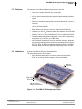
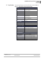
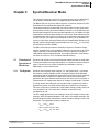
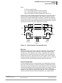
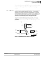
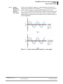
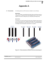
DNx-AI-255 — User Manual 2-Channel Synchro/Resolver I/O Interface Layer for the PowerDNA Cube and PowerDNR RACKtangle USPTO Patent: 7,957,942 Release 4.5 February 2012 PN Man-DNx-AI-255-212-DRAFT © Copyright 1998-2012 United Electronic Industries, Inc. All rights reserved. No part of this publication may be reproduced, stored in a retrieval system, or transmitted, in any form by any means, electronic, mechanical, by photocopying, recording, or otherwise without prior written permission. Information furnished in this manual is believed to be accurate and reliable. However, no responsibility is assumed for its use, or for any infringement of patents or other rights of third parties that may result from its use. All product names listed are trademarks or trade names of their respective companies. See the UEI website for complete terms and conditions of sale: http://www.ueidaq.com/cms/terms-and-conditions/ Contacting United Electronic Industries Mailing Address: 27 Renmar Avenue Walpole, MA 02081 U.S.A. For a list of our distributors and partners in the US and around the world, please see http://www.ueidaq.com/partners/ Support: Telephone: Fax: (508) 921-4600 (508) 668-2350 Also see the FAQs and online “Live Help” feature on our web site. Internet Support: Support: Web-Site: FTP Site: [email protected] www.ueidaq.com ftp://ftp.ueidaq.com Product Disclaimer: WARNING! DO NOT USE PRODUCTS SOLD BY UNITED ELECTRONIC INDUSTRIES, INC. AS CRITICAL COMPONENTS IN LIFE SUPPORT DEVICES OR SYSTEMS. Products sold by United Electronic Industries, Inc. are not authorized for use as critical components in life support devices or systems. A critical component is any component of a life support device or system whose failure to perform can be reasonably expected to cause the failure of the life support device or system, or to affect its safety or effectiveness. Any attempt to purchase any United Electronic Industries, Inc. product for that purpose is null and void and United Electronic Industries Inc. accepts no liability whatsoever in contract, tort, or otherwise whether or not resulting from our or our employees' negligence or failure to detect an improper purchase. Specifications in this document are subject to change without notice. Check with UEI for current status. DNA/DNR-AI-255 Synchro/Resolver Interface Contents Table of Contents Chapter 1 Introduction .................................................... 1 1.1 Organization of Manual. . . . . . . . . . . . . . . . . . . . . . . . . . . . . . . . . . . . . . . . . . . . . . . . 1 1.2 The AI-255 Interface Board. . . . . . . . . . . . . . . . . . . . . . . . . . . . . . . . . . . . . . . . . . . . . 3 1.3 Features . . . . . . . . . . . . . . . . . . . . . . . . . . . . . . . . . . . . . . . . . . . . . . . . . . . . . . . . . . . 4 1.4 Indicators . . . . . . . . . . . . . . . . . . . . . . . . . . . . . . . . . . . . . . . . . . . . . . . . . . . . . . . . . . 4 1.5 Specification . . . . . . . . . . . . . . . . . . . . . . . . . . . . . . . . . . . . . . . . . . . . . . . . . . . . . . . . 5 Chapter 2 Synchro/Resolver Mode .......................................... 6 2.1 2.1.1 2.1.2 Overview of Synchros & Resolvers. . . . . . . . . . . . . . . . . . . . . . . . . . . . . . . . . . . . . . . 6 The Synchro. . . . . . . . . . . . . . . . . . . . . . . . . . . . . . . . . . . . . . . . . . . . . . . . . . . 6 The Resolver . . . . . . . . . . . . . . . . . . . . . . . . . . . . . . . . . . . . . . . . . . . . . . . . . . 8 2.2 Device Architecture. . . . . . . . . . . . . . . . . . . . . . . . . . . . . . . . . . . . . . . . . . . . . . . . . . 13 2.3 Setting Operating Parameters . . . . . . . . . . . . . . . . . . . . . . . . . . . . . . . . . . . . . . . . . 14 2.4 Pinout . . . . . . . . . . . . . . . . . . . . . . . . . . . . . . . . . . . . . . . . . . . . . . . . . . . . . . . . . . . . 14 2.5 Synchro-Resolver Wiring Connections . . . . . . . . . . . . . . . . . . . . . . . . . . . . . . . . . . . 15 Chapter 3 Programming with the High Level API . . . . . . . . . . . . . . . . . . . . . . . . . . . . . . 19 3.1 Creating a Session . . . . . . . . . . . . . . . . . . . . . . . . . . . . . . . . . . . . . . . . . . . . . . . . . . 20 3.2 Configuring the Resource String. . . . . . . . . . . . . . . . . . . . . . . . . . . . . . . . . . . . . . . . 20 3.3 Configuring for Input . . . . . . . . . . . . . . . . . . . . . . . . . . . . . . . . . . . . . . . . . . . . . . . . . 20 3.4 Simulated Synchro/Resolver Output. . . . . . . . . . . . . . . . . . . . . . . . . . . . . . . . . . . . . 21 3.5 Configuring the Timing . . . . . . . . . . . . . . . . . . . . . . . . . . . . . . . . . . . . . . . . . . . . . . . 21 3.6 Read Data. . . . . . . . . . . . . . . . . . . . . . . . . . . . . . . . . . . . . . . . . . . . . . . . . . . . . . . . . 22 3.7 Write Data . . . . . . . . . . . . . . . . . . . . . . . . . . . . . . . . . . . . . . . . . . . . . . . . . . . . . . . . . 22 3.8 Cleaning-up the Session. . . . . . . . . . . . . . . . . . . . . . . . . . . . . . . . . . . . . . . . . . . . . . 22 Chapter 4 Programming with the Low-level API . . . . . . . . . . . . . . . . . . . . . . . . . . . . . . . 23 4.1 4.1.1 DNx-AI-255 Modes of Operation. . . . . . . . . . . . . . . . . . . . . . . . . . . . . . . . . . . . . . . . 24 Wiring. . . . . . . . . . . . . . . . . . . . . . . . . . . . . . . . . . . . . . . . . . . . . . . . . . . . . . . 25 4.2 Low‒Level Functions . . . . . . . . . . . . . . . . . . . . . . . . . . . . . . . . . . . . . . . . . . . . . . . . 27 © Copyright 2012 United Electronic Industries, Inc. Tel: 508-921-4600 Date: February 2012 www.ueidaq.com Vers: 4.5 DNx-AI-255-ManualTOC.fm iii DNA/DNR-AI-255 Synchro/Resolver Interface Figures List of Figures 1-1 2-1 2-2 2-3 2-4 2-5 2-6 2-7 2-8 2-9 2-10 2-11 2-12 A-1 B-1 B-2 B-3 B-4 B-5 B-6 B-7 B-8 B-9 B-10 The DNR-AI-255 Analog-Input Layer............................................................................ 4 Typical Synchro Transmitter/Receiver .......................................................................... 7 Brushless Resolver Control Transformer...................................................................... 8 SIN and COS Output Voltages vs. Rotor Angle............................................................ 9 Resolver Waveforms at 30° Rotor Angle .................................................................... 10 Resolver Waveforms at 135° Rotor Angle .................................................................. 10 Resolver Waveforms at 45° Rotor Angle .................................................................... 11 Synchro Waveforms at 0° Rotor Angle. ...................................................................... 11 Magnitudes of SIN and COS Output RMS Voltages vs. Rotor Angle ......................... 12 Block Diagram of DNx-AI-255 I/O Board .................................................................... 13 Pinout Diagram for DNx-AI-255 .................................................................................. 14 Peak-to-peak voltage measurement of Synchro......................................................... 16 Connection in Z-grounded mode of Synchro .............................................................. 17 Pinout and photo of DNA-STP-62 screw terminal panel............................................. 28 AI-255 in Synchro Input Mode with Internal Excitation ............................................... 29 AI-255 in Synchro Input Mode with External Excitation .............................................. 30 AI-255 in Synchro Simulator Mode with Internal Excitation ........................................ 31 PowerDNA Explorer in Simulator Mode, Int. Exc., 180º ............................................. 32 Waveforms for Simulator Mode w/ Int. Exc. at 0º (left) and 180º (right)...................... 32 AI-255 in Synchro Simulator Mode with External Excitation ....................................... 33 AI-255 in Resolver Input Mode with Internal Excitation .............................................. 35 AI-255 in Resolver Input Mode with External Excitation ............................................. 36 AI-255 in Resolver Simulator Mode with Internal Excitation ....................................... 37 AI-255 in Resolver Simulator Mode with External Excitation ...................................... 38 © Copyright 2012 United Electronic Industries, Inc. Tel: 508-921-4600 Date: February 2012 www.ueidaq.com Vers: 4.5 DNx-AI-255-ManualLOF.fm iv DNA/DNR-AI-255 Synchro/Resolver Interface Chapter 1 Introduction Chapter 1 Introduction This document outlines the feature-set of the DNR- and DNA-AI-255 layer and how to use it for synchro/resolver applications. 1.1 Organization of Manual © Copyright 2012 United Electronic Industries, Inc. This AI-255 User Manual is organized as follows: • Introduction This section provides an overview of the AI-255 features. • Synchro/Resolver Input and Output/Simulator This chapter provides an introduction to the synchro/resolver interface features, device architecture, and connectivity of the AI-256. • Programming with the High-Level API This chapter provides an overview of the how to create a session, configure the session, and format relevant data with the Framework API. • Programming with the Low-Level API Describes low-level API commands for configuring and using the AI-255 series layer for Synchro/Resolver/LVDT/RVDT operating modes. • Appendix A - Accessories This appendix provides a list of accessories available for use with the DNx-AI-255 Synchro/Resolver interface board. • Appendix B - Connection Diagrams This appendix contains connection diagrams for various operating and synchro/resolver excitation modes of the DNx-AI-255 interface board. • Index This is an alphabetical listing of the topics covered in this manual. Tel: 508-921-4600 Date: February 2012 www.ueidaq.com Vers: 4.5 DNx-AI-255 Chap1x.fm 1 DNA/DNR-AI-255 Synchro/Resolver Interface Chapter 1 Introduction Manual Conventions To help you get the most out of this manual and our products, please note that we use the following conventions: Tips are designed to highlight quick ways to get the job done or to reveal good ideas you might not discover on your own. NOTE: Notes alert you to important information. CAUTION! Caution advises you of precautions to take to avoid injury, data loss, and damage to your boards or a system crash. Text formatted in bold typeface generally represents text that should be entered verbatim. For instance, it can represent a command, as in the following example: “You can instruct users how to run setup using a command such as setup.exe.” Text formatted in fixed typeface generally represents source code or other text that should be entered verbadim into the source code, initialization, or other file. Examples of Manual Conventions Before plugging any I/O connector into the Cube or RACKtangle, be sure to remove power from all field wiring. Failure to do so may cause severe damage to the equipment. Usage of Terms Throughout this manual, the term “Cube” refers to either a PowerDNA Cube product or to a PowerDNR RACKtangle rack mounted system, whichever is applicable. The term DNR is a specific reference to the RACKtangle, DNA to the PowerDNA I/O Cube, and DNx to refer to both. © Copyright 2012 United Electronic Industries, Inc. Tel: 508-921-4600 Date: February 2012 www.ueidaq.com Vers: 4.5 DNx-AI-255 Chap1x.fm 2 DNA/DNR-AI-255 Synchro/Resolver Interface Chapter 1 Introduction 1.2 The AI-255 Interface Board The DNx-AI-255 layer can act as a 2-channel synchro or resolver input or simulator output interface. It is suited for a wide variety of industrial, military, and simulator applications. The AI-255 functionality is similar to the AI-256, and uses the same subset of Synchro/Resolver software functions as the AI-256, but operates at lower frequency, lower currents and higher voltages than the AI-256. The board provides two channels that can monitor either 3/4-wire (plus excitation) synchros or 4-wire (plus rotor excitation) resolvers or, as an alternative, provide simulated outputs for test and simulator applications. It is capable of angle measurement accuracies approaching ±2.6 arc-minutes. Each channel may be configured either as an input or an output, in any combination. Output accuracy is ±4 arc-minutes. The inputs may be sampled at rates up to the excitation frequency of 4 kHz. Each channel provides its own Programmable Reference Voltage with outputs independently programmable from 2 to 28 Vrms at 1.2 VA and at frequencies from 50 to 4000Hz. The DNx-AI-255 also provides two channels of Synchro or Resolver Output, ideal for driving devices such as attitude indicators or as test sources for a wide range of synchro or resolver input devices. The two outputs each accept an independent reference signal and offer 16-bit output resolution. Each channel can drive up to 28 Vrms at 1.2 VA without external buffering. The AI-255 is available in two versions: the DNA-AI-255 for mounting in UEI Cube products, and the DNR-AI-255 for insertion into the UEI RACKtangle and HalfRACK chassis. The DNx-AI-255 is physically a two-board module composed of one of two types of base boards (one for the DNA version and another for the DNR version) plus an AI-255-specific daughter board. The DNA and DNR are functionally the same except for the bus connectors used. The DNx-AI-255 is fully supported by the UEIDAQ Framework API, which provides a simple and complete software interface to all popular programming languages, operating systems, and data acquisition/control application packages such as LabVIEW, DASYLab, and MATLAB. As with all UEI PowerDNA boards, the DNx-AI-255 can be operated in harsh environments and has been tested at 5g vibration, 50g shock, -40 to +85°C temperature, and altitudes up to 70,000 feet. Each board provides 350 Vrms isolation between channels and also between the board and its enclosure or any other installed boards as well as electro-shock-discharge (ESD) isolation. Software for the DNx-AI-255 is provided as part of the UEI Framework. Framework provides a comprehensive, yet easy-to-use, API that is compatible with all popular Windows programming languages and that also supports programmers using Linux and most realtime operating systems such as QNX, RTX, or RT Linux. Also, UEI Framework can be used for creating applications in LabVIEW, MATLAB/SImulink, DASYLab, or any application that supports ActiveX or OPC servers. © Copyright 2012 United Electronic Industries, Inc. Tel: 508-921-4600 Date: February 2012 www.ueidaq.com Vers: 4.5 DNx-AI-255 Chap1x.fm 3 DNA/DNR-AI-255 Synchro/Resolver Interface Chapter 1 Introduction 1.3 1.4 Features Indicators The features of the DNx-AI-255 that are important to note are: • Two input or output channelsin any combination • 16-bit Resolution • 3/4-wire (plus excitation) Synchro and 4-wire (plus excitation) Resolver Inputs • Reference (excitation) Output (28 Vrms) for each channel with 1.2 mVrms resolution • User-programmable Excitation Frequency Range of 50 Hz to 4 kHz (±0.5%) for Each Channel • Each channel can drive up to 28 Vrms without External Buffering • Isolation up to 350 Vrms between channel and between I/O’s and GND • Weight of 136 g or 4.79 oz for DNA-AI-255; 817 g or 28.8 oz with PPC5. • Tested to withstand 5g Vibration, 50g Shock, -40 to +85°C Temperature, and Altitude up to 70,000 ft or 21’000 meters. • UEI Framework Software API may be used with all popular Windows programming languages and most real time operating systems such as RT Linux, RTX, or QNX and graphical applications such as LabVIEW, MATLAB, DASYLab and any application supporting ActiveX or OPC. A photo of the DNx-AI-255 unit is illustrated below. The front panel has two LED indicators: • RDY: indicates that the layer is receiving power and operational. • STS: can be set by the user using the low-level framework. DNA bus connector RDY LED STS LED DB-62 (female) 62-pin I/O connector Figure 1-1. The DNR-AI-255 Analog-Input Layer © Copyright 2012 United Electronic Industries, Inc. Tel: 508-921-4600 Date: February 2012 www.ueidaq.com Vers: 4.5 DNx-AI-255 Chap1x.fm 4 DNA/DNR-AI-255 Synchro/Resolver Interface Chapter 1 Introduction 1.5 Specification The technical specification for the DNx-AI-255 board are listed in Table 1-1. Table 1-1. DNx-AI-255 Technical Specifications Inputs Number of channels Configuration Resolution Accuracy Frequency Signal Inputs Acceleration Step response Update rate Reference output Number of channels Output voltage Voltage resolution Reference Frequency Synchro / Resolver Outputs Number of channels Configuration Resolution Output Voltage Output Accuracy General Specifications Operating temperature Vibration IEC 60068-2-6 IEC 60068-2-64 Shock IEC 60068-2-27 Humidity Altitude MTBF © Copyright 2012 United Electronic Industries, Inc. Tel: 508-921-4600 Date: February 2012 2 Synchro (3-wire) or Resolver (4-wire) may be selected via software 16-bit ± 2.6 arc-minute 50 Hz to 4.0 kHz 2-28 Vrms. 300 rps/s @ 60 Hz 450 rps/s @ 400 Hz 1000 rps/s @ 4000 Hz 800 mS - 179° @ 60 Hz 150 mS - 179° @ 2500 Hz Maximum update rate is equal to the excitation frequency. 2 (one per input channel) 28 Vrms up to 1.2 VA. 1.2 mVrms 50 Hz to 4 kHz (±0.5%) 2 (total number of synchro/resolver inputs and simulated outputs is limited to 2.) Synchro (3-wire) or Resolver (4-wire) 16-bit 28 Vrms up to 1.2 VA. ±4 arc-minutes Tested -40 °C to +85 °C 5 g, 10-500 Hz, sinusoidal 5 g (rms), 10-500 Hz, broad-band random 50 g, 3 ms half sine, 18 shocks @ 6 orientations 30 g, 11 ms half sine, 18 shocks @ 6 orientations 5 to 95%, non-condensing 0 to 70,000 feet 275,000 hours www.ueidaq.com Vers: 4.5 DNx-AI-255 Chap1x.fm 5 DNA/DNR-AI-255 Synchro/Resolver Interface Chapter 2 Synchro/Resolver Mode Chapter 2 Synchro/Resolver Mode This chapter provides an overview of synchros/resolvers, how the DNx-AI-255 can be used to manipulate them, and supporting documentation to do so. The DNx-AI-255 can act as a 2-channel Synchro or Resolver interface for UEI’s PowerDNA and PowerDNR data acquisition systems. The board provides two channels that can monitor either 3/4-wire (plus excitation) synchros or 4-wire (plus rotor excitation) resolvers or, as an alternative, provide simulated outputs for test and simulator applications. It is capable of angle measurement accuracies approaching ±2.6 arc-minutes. Each channel may be configured either as an input or an output, in any combination. Output accuracy is ±4 arc-minutes. The inputs may be sampled at rates up to the excitation frequency of 4 kHz. Each channel provides its own Programmable Reference Voltage with outputs independently programmable from 2 to 28 Vrms at 1.2 VA and at frequencies from 50 to 4000Hz. The DNx-AI-255 also provides two channels of Synchro or Resolver Output, ideal for driving devices such as attitude indicators or as test sources for a wide range of synchro or resolver input devices. The two outputs each accept an independent reference signal and offer 16-bit output resolution. Each channel can drive up to 28 Vrms at 1.2 VA without external buffering. 2.1 2.1.1 Overview of Synchros & Resolvers Synchros and resolvers are electromechanical transducers that are used either to detect and measure a rotary shaft position or to position a shaft at a desired angle. The devices can be further classified as transmitters, receivers, differentials, or control transformers. The Synchro Synchros were originally called “selsyns”, for “self-synchronous”. A generator and receiver are wired together so that the angular position of the generator (transmitter) shaft is automatically reproduced in the motor (receiver). Although they may appear to be similar in construction to synchronous motors and generators, the major difference between them is that the rotor of a synchro is excited with an AC voltage rather than a DC voltage. In other words, a synchro is a single phase device with AC rotor excitation and a synchronous motor or generator is typically a 3-phase (time-phase) device with DC rotor excitation. The rotor of a synchro normally has a single-phase winding, usually referred to as a “dumbbell” rotor. The stator has 3 windings connected in a star configuration at 120°. The AC voltage applied to the rotor winding induces AC voltages in three stator windings, which are spatially displaced 120° apart. The voltages induced in the stator windings are either in time-phase with the excitation voltage or 180° out of time-phase. The magnitudes of these voltages are: VS1-3 = KVR2-1 sin θ VS3-2 = KVR2-1 sin (θ + 120°) VS2-1 = KVR2-1 sin (θ + 240°) © Copyright 2012 United Electronic Industries, Inc. Tel: 508-921-4600 Date: February 2012 www.ueidaq.com Vers: 4.5 DNx-AI-255 Chap2.fm 6 DNA/DNR-AI-255 Synchro/Resolver Interface Chapter 2 Synchro/Resolver Mode where θ is the rotor position angle VS1-3 is the voltage between S1 and S3 terminals VR2-1 is the voltage between R2 and R1 terminals and K is the maximum coupling transformation ratio Vout/Vin Since the set of three voltages transmitted by the synchro generator is unique for each position of the rotor throughout a 360° rotation, a synchro receiver, whose rotor is excited in parallel with the generator, measures the magnitude and time-phase relation of the voltages and produces a torque that causes the receiver rotor to move to the same angular position as the transmitter. A synchro transmitter and receiver thus form a simple synchro system. S1 C S2 C S3 C S1 C S2 C S3 C Stator Stator Rotor Rotor R1 R2 CG Transmitter R1 R2 AC Excitation Source CR Receiver Figure 2-1. Typical Synchro Transmitter/Receiver Receiver When the transmitter and receiver rotors are in alignment, stator voltages are equal and no current flows. If the transmitter rotor is turned (relative to the receiver rotor), a force appears in the receiver, causing the rotor to track the transmitter rotor. The torque produced is proportional to the angle difference between the two rotors. Typical accuracy of such a system is 30 arc-minutes. A single transmitter may be parallel-connected to multiple receivers, at the cost of reducing accuracy and increasing the power drain from the source. Control Transformer A control transformer has a Y-connected stator and a single-phase cylindrical drum rotor. When the stator is connected to the stator of a transmitter and the transmitter rotor is turned relative to the control transformer rotor, the magnitude of the control transformer stator field remains constant, but a voltage is induced in the rotor. The magnitude of this voltage varies with the sine of the angle between the axis of the rotor and that of the stator flux. The control transformer, therefore, provides information about the transmitter rotor angular position. © Copyright 2012 United Electronic Industries, Inc. Tel: 508-921-4600 Date: February 2012 www.ueidaq.com Vers: 4.5 DNx-AI-255 Chap2.fm 7 DNA/DNR-AI-255 Synchro/Resolver Interface Chapter 2 Synchro/Resolver Mode If the control transformer rotor angle differs from that of the transmitter, a voltage proportional to the sine of the angular difference appears on the control transformer rotor. This may be used as an input to a servo control system that causes the control transformer rotor to move to the same angle as the transmitter. 2.1.2 The Resolver A resolver is a rotary transformer in which the magnitude of the energy through the resolver varies sinusoidally with rotation of the shaft. A resolver control transmitter has one primary winding (Reference Winding) and two secondary windings (the SIN and COS windings). The reference winding is located on the rotor and the SIN and COS windings are on the stator, displaced spatially by 90°. If the resolver is a brushless type, current is applied through a rotary transformer, which eliminates the problems of slip rings and brushes. The reference winding is typically excited by an AC voltage. The induced voltages in the SIN and COS windings are equal to the reference voltage multiplied by the sine or cosine of the angle of the input shaft relative to a fixed zero position. The connection arrangement of a brushless resolver control transformer is illustrated below in Figure 2-2. S4 COS Winding Vc = Vr cos T S2 R1 SIN Winding Vr R2 Rotary Transformer T S3 Vc = Vr sin T S1 Figure 2-2. Brushless Resolver Control Transformer © Copyright 2012 United Electronic Industries, Inc. Tel: 508-921-4600 Date: February 2012 www.ueidaq.com Vers: 4.5 DNx-AI-255 Chap2.fm 8 DNA/DNR-AI-255 Synchro/Resolver Interface Chapter 2 Synchro/Resolver Mode 2.1.2.1 Voltage Magnitude, Polarity, and Phase vs. Rotor Angle A sine wave AC Excitation voltage Vexcis applied between R1 and R2. The voltage observed between S1 and S3 is Vsin = Vexc sin A, where A is the rotor angle in radians. SImilarly, the voltage observed between S2 and S4 is Vcos = Vexc cos A, where A is the rotor angle in radians. The two output voltages remain in phase with each other relative to the excitation voltage, but differ in magnitude and/or polarity (relative to excitation) as the rotor angle changes, as shown in Figure 2-3. Figure 2-3. SIN and COS Output Voltages vs. Rotor Angle © Copyright 2012 United Electronic Industries, Inc. Tel: 508-921-4600 Date: February 2012 www.ueidaq.com Vers: 4.5 DNx-AI-255 Chap2.fm 9 DNA/DNR-AI-255 Synchro/Resolver Interface Chapter 2 Synchro/Resolver Mode COS output SIN output Excitation Figure 2-4. Resolver Waveforms at 30° Rotor Angle Referring to 2-4, The SIN and COS output voltages are in phase with excitation, have the same polarity relative to excitation, but have different magnitudes. Referring to 2-5, The SIN and COS output voltages are in phase with excitation, have the opposite polarity relative to excitation, but have equal magnitudes. SIN output COS output Excitation Figure 2-5. Resolver Waveforms at 135° Rotor Angle © Copyright 2012 United Electronic Industries, Inc. Tel: 508-921-4600 Date: February 2012 www.ueidaq.com Vers: 4.5 DNx-AI-255 Chap2.fm 10 DNA/DNR-AI-255 Synchro/Resolver Interface Chapter 2 Synchro/Resolver Mode SIN output COS output Excitation Figure 2-6. Resolver Waveforms at 45° Rotor Angle Referring to 2-6, The SIN and COS output voltages are in phase with excitation, have the same polarity relative to excitation, and also have equal magnitudes. When a synchro is used, the excitation and output voltages appear as shown in Figure 2-7. Note that a synchro has three windings with angles between coils of 120°. S3 (Cyan) S2 (Blue) S1 (Green) Excitation Figure 2-7. Synchro Waveforms at 0° Rotor Angle. © Copyright 2012 United Electronic Industries, Inc. Tel: 508-921-4600 Date: February 2012 www.ueidaq.com Vers: 4.5 DNx-AI-255 Chap2.fm 11 DNA/DNR-AI-255 Synchro/Resolver Interface Chapter 2 Synchro/Resolver Mode The SI coil output voltage (green line) is zero because the rotor is positioned plus or minus 90° relative to the S1 stator winding and therefore produces nothing. The S2 coil (blue line) shows a voltage in phase with excitation and with the same polarity as the excitation voltage. The S3 coil (cyan line) shows a voltage of polarity opposite to that of the excitation (or 180° out of phase). NOTE: Coils on a synchro can be labeled in two different ways -- looking at the synchro from the shaft side as S1at the top, followed in a counterclockwise direction by S2 and S3, or looking at the collector side as S1 at the top, followed in a clockwise direction by S2 and S3. In datasheets from some companies, the labeling may be reversed. NOTE: When using the AI-255 for simulation, you can attach a scope to the simulation outputs, ground the scope probes to AGND and read voltages between S1 and AGND, S2 and AGND, and S3 and AGND. Some synchros have the coil mid points between coils brought out, but most do not. To create a proper transform function, you need to consider the following formula: ϕ actual = 135deg – ϕ calculated where the angle is calculated from the scope display. Figure 2-8 below illustrates how the magnitudes of the SIN and COS output voltages vary with rotor angle. The table that follows lists the calculated data points for the graph. Resolver Output vs. Shaft Angle SIN 1.5 COS 1 0 39 0 36 0 33 0 30 0 27 0 24 0 21 0 18 0 15 0 12 90 60 30 0 0 Output 0.5 -0.5 -1 -1.5 Shaft Angle Figure 2-8. Magnitudes of SIN and COS Output RMS Voltages vs. Rotor Angle © Copyright 2012 United Electronic Industries, Inc. Tel: 508-921-4600 Date: February 2012 www.ueidaq.com Vers: 4.5 DNx-AI-255 Chap2.fm 12 DNA/DNR-AI-255 Synchro/Resolver Interface Chapter 2 Synchro/Resolver Mode A block diagram of a DNx-AI-255 board is shown in Figure 2-9. P G A A D C 32-bit 66MHz BUS DACs LOGIC AIN+ AINBIN+ BINCIN+ CINDIN+ DIN- Analog In/Out Connector Synchro / Resolver or Avionics Equip. Channel 0 Internal Excitation or Analog Outputs OUTA+ OUTAOUTB+ OUTBOUTC+ OUTCOUTD+ OUTD- ISOLATION Device Architecture Overvoltage Protection 2.2 Channel 1 (Same as Channel 0) External Excitation DC/DC Note: Refer to Appendix B for connection diagrams Figure 2-9. Block Diagram of DNx-AI-255 I/O Board As shown in Figure 2-9, board logic is divided into isolated and non-isolated sections. The non-isolated logic complies with the full UEI Common Logic Interface standard. The isolated side handles all functions associated with the sensor input and output circuits.The non-isolated side handles all Cube or chassis-related operations. Referring to Fig. 2-9, the two analog inputs from the synchro or resolver sensor are input to the programmable gain amplifiers (one per input pair) as differential inputs. Selected gain and offset are applied, producing single-ended outputs. These outputs are then converted to differential signals for input to 16-bit SAR analog to digital converters. These converters have serial interface outputs. The signals from the ADC are passed to a 16-bit quad DAC, combined with +VREF voltage, amplified, and output to a sensor/resolver or avionic hardware. Refer to Appendix B for connection diagrams. © Copyright 2012 United Electronic Industries, Inc. Tel: 508-921-4600 Date: February 2012 www.ueidaq.com Vers: 4.5 DNx-AI-255 Chap2.fm 13 DNA/DNR-AI-255 Synchro/Resolver Interface Chapter 2 Synchro/Resolver Mode The DACs may be written from multiple sources, such as: • Direct DAC write registers • Direct DAC output word register • Output FIFO. 1024 word FIFO may be used to hold DAC values or commands (in simulation mode) • Waveform generator — which permits you to output a preloaded waveform on the output channels for simulation purposes • Combination waveform and FIFO with FIFO in command mode — In this mode, output from FIFO may be directed to phase or gain registers or change may be delayed until the index of waveform is equal to zero. The logic computes moving averages of all analog inputs (updated with each sample) and also computes other values like (Sa-Sb)/(Sa+Sb) or (Sa-Sb)/Se, where Sa and Sb are computed values of moving averages of analog inputs and Se is the moving average of the excitation voltage value. Timing is controlled by counting pulses in half periods between zero crossings of the reference voltage signal. More information about the computations performed is available in Chapters 3 and 4 and the API Reference Manuals that describe the high-level and low-level functions used with this layer. 2.3 Setting Operating Parameters For detailed instructions for configuring the board and setting operating modes and parameters, refer to the Functions DqAdv255SetMode, DqAdv255SetExcitation, and DqAdv255GetWFMeasurements, which are described in Chapter 3 and also in the PowerDNA API Reference Manual. 2.4 Pinout The pinout of the DNx-AI-255 62-pin DB connector is shown in Figure 2-10. Pinout Diagram: Chan 0 Chan 1 Pin 1 2 3 4 5 6 7 8 9 10 11 12 13 14 15 16 17 18 19 20 21 Signal Rsvd Out B+ Rsvd In A+ In B+ Gnd Out C+ Out D+ In C+ In D+ Rsvd Out B+ Rsvd In A+ In B+ Gnd Out C+ Out D+ Rsvd In D+ Rsvd Pin 22 23 24 25 26 27 28 29 30 31 32 33 34 35 36 37 38 39 40 41 42 Signal Gnd Out Bn/c In AIn BRsvd Out COut DIn CIn Dn/c Out BGnd In AIn BRsvd Out COut DGnd In Dn/c Pin 43 44 45 46 47 48 49 50 51 52 53 54 55 56 57 58 59 60 61 62 Signal Out AOut A+ Gnd Rsvd n/c Rsvd Rsvd Rsvd Gnd Rsvd Out AOut A+ Gnd Rsvd n/c Rsvd n/c Rsvd In CIn C+ Dashed Line represents the isolation barrier between channels Figure 2-10. Pinout Diagram for DNx-AI-255 © Copyright 2012 United Electronic Industries, Inc. Tel: 508-921-4600 Date: February 2012 www.ueidaq.com Vers: 4.5 DNx-AI-255 Chap2.fm 14 DNA/DNR-AI-255 Synchro/Resolver Interface Chapter 2 Synchro/Resolver Mode Before plugging any I/O connector into the Cube or RACKtangle, be sure to remove power from all field wiring. Failure to do so may cause severe damage to the equipment. 2.5 SynchroResolver Wiring Connections The table shown below (Table 2-1) matches the terminal connections of the AI-255 with the corresponding terminals on a synchro or a resolver device or simulator in each of the various operating modes. For a synchro, the terminals are S1, S2, S3 and C for the three stator windings and common and R1, R2 for the rotor. For a resolver, the terminals are S1/S3 and S2/S4 for stator windings and R1/R2 for the rotor. Exc+ and Exc– refer to excitation. For Connection Diagrams of the various modes, see Appendix B. Table 2-1. Synchro-Resolver Wiring Connections for Various Modes Signal Name Pin No. Ch 0 Input Mode, Internal Excitation Input Mode, External Excitation Simulator Mode, Simulator Mode, Internal Excitation External Excitation Ch 1 Synchro Resolver Synchro Resolver Synchro Resolver Synchro Resolver In A+ 4 14 S1 S1 S1 S1 NC NC NC NC In A- 25 35 C S3 C S3 NC NC NC NC In B+ 5 15 S3 S2 S3 S2 NC NC NC NC In B- 26 36 C S4 C S4 NC NC NC NC In C+ 9 62 S2 NC S2 NC NC NC NC NC In C- 30 61 C NC C NC NC NC NC NC In D+ 10 20 NC NC Exc+ Exc+(R1) NC NC Exc+ Exc+ In D- 31 41 NC NC Exc- Exc-(R2) NC NC Exc- Exc- OutA+ 44 54 NC NC NC NC S1 S1 S1 S1 OutA- 43 53 NC NC NC NC C S3 C S3 OutB+ 2 12 NC NC NC NC S3 S2 S3 S2 OutB- 23 33 NC NC NC NC C S4 C S4 OutC+ 7 17 NC NC(R2) NC NC S2 Opt+(R2) S2 NC OutC- 28 38 NC NC(R4) NC NC C Opt-(R4) C NC OutD+ 8 18 R1 R1 NC NC Exc+ Exc+(R1) NC NC OutD- 29 39 R2 R3 NC NC Exc- Exc-(R3) NC NC NC 24,47 32, 42, 57, 59 -- -- -- -- -- -- -- -- GND 6, 22, 16, 34, 45, 51 40, 55 -- -- -- -- -- -- -- -- Rsvd 1, 3, 27, 46, 48, 49, 50, 52 11, 13, 19, 21, 37, 56, 58, 60 -- -- -- -- -- -- -- -- © Copyright 2012 United Electronic Industries, Inc. Tel: 508-921-4600 Date: February 2012 www.ueidaq.com Vers: 4.5 DNx-AI-255 Chap2.fm 15 DNA/DNR-AI-255 Synchro/Resolver Interface Chapter 2 Synchro/Resolver Mode The AI-255 performs measurement and stimulation to attached synchros and resolvers by comparing each of the inputs (S1, S2, S3) to a ground reference line at the AI-255’s ADC using peak-to-peak voltage (Vpp) values. S1 S3 VPPS3 S2 VPPS2 TBD DNx-AI-255 Layer DAC Phase Correction PowerDNA Driver VPPS1 VPP values to sw app Line-to-Line & Peak-to-Peak Measurement Result to User 2.5.0.1 Synchro Figure 2-11. Peak-to-peak voltage measurement of Synchro The synchro, however, is most commonly rated to use the root mean squared (rms) voltage as measured between two lines (not ground referenced). This is the rms line to line voltage (VLL) measured across two of the three stator wires (VS1-3, VS3-2, or VS2-1; as seen on page 6) or the excitation wires (Vext+, Vext-). The user must convert between the line-to-line RMS voltage amplitude (VLL) from the synchro specification and the peak-to-peak output-to-ground voltage amplitude (VPP) that is the parameter needed by the AI-255 driver. Convert between VLL and VPP with the relation: V LL V PP = 2 2 --------------------------- ≅ 1.63299V LL 2 sin ( 120° ) or using the low-level software macro from powerdna.h: #define DQ_AI255_RMS_LN_LN_TO_PP(V) ((V)*1.633) where input parameter V is VLL, and the resulting output is VPP. Additionally, the low-level API also defines a macro to convert from VLL to VRMS: #define DQ_AI255_RMS_LN_LN_TO_RMS(V) ((V)*0.5774) where input parameter V is the line-to-line voltage VLL, and the result is in volts RMS referenced to ground (VRMS). The constant 0.5774 is 1/(2·sin(120º)). As an example, a synchro with the rms excitation voltage of 23.5V between Vext+ and Vext- will need a ground-referenced peak-to-peak voltage of 66.4V set for the AI-255, since 66.4V ≈ 2·√(2)·23.5V (no phase adjustment necessary). The same synchro’s rms stator voltage of 11.8V that is the rms voltage between any two stator connections (responsible for positioning the rotor) should have a maximum peak-to-peak voltage span of 19.26V ≈ 11.8V/1.633·2·√(2). © Copyright 2012 United Electronic Industries, Inc. Tel: 508-921-4600 Date: February 2012 www.ueidaq.com Vers: 4.5 DNx-AI-255 Chap2.fm 16 DNA/DNR-AI-255 Synchro/Resolver Interface Chapter 2 Synchro/Resolver Mode Exercise caution when wiring and double-check that correct voltage is set on the AI-255 to avoid overloading and permanently damaging the synchro or resolver. In Figure 2-11 on page 16, once the data has been sampled, the Cube logic corrects the phase by subtracting 30º, 150º, and 270º from S1, S2, and S3 resulting waveforms to yield an ideal voltage representation. This transformation is transparent, the final result appears as the final VPP value to user application. 2.5.0.2 Z-grounded mode It is possible to ground the z (S3) lines of some synchros to the vehicle’s common ground to save on wiring - this is called a synchro in z-grounded mode. For z-grounded synchros, the S3 input/output on the AI-255 is left unconnected. The mode must be set for the AI-255 in software when using z-grounded mode. The modes for the low-level API are listed in the table below; refer to Chapter 4 for information on low-level software programming. Mode of Operation Description DQ_AI255_MODE_SI_INTZ Synchro input, int. exc., Z grounded DQ_AI255_MODE_SI_EXTZ Synchro input, ext. exc., Z grounded DQ_AI255_MODE_SS_INTZ Synchro output, int. exc., Z grounded DQ_AI255_MODE_SS_EXTZ Synchro output, ext. exc., Z grounded Table 2-2. Z-grounded modes of operation from powerdna.h The connection diagram for wiring a synchro in z-grounded mode is as follows: S1 VPPS1 DAC VPPS3 S2 VPPS2 S3 TBD AI-256 AGND Synchro Figure 2-12. Connection in Z-grounded mode of Synchro © Copyright 2012 United Electronic Industries, Inc. Tel: 508-921-4600 Date: February 2012 www.ueidaq.com Vers: 4.5 DNx-AI-255 Chap2.fm 17 DNA/DNR-AI-255 Synchro/Resolver Interface Chapter 2 Synchro/Resolver Mode 2.5.0.3 Troubleshooting This section describes some of the symptoms observed when the synchro is not wired correctly to the layer. Incorrect wiring can be as mild as inaccurate rotor position or as severe as permanently damaging the synchro. In the mildest cases, the synchro or rotor lines may be in incorrect positions in the terminal panel. Reversing the rotor (Vext+, Vext-) or stator (S1, S2, S3) wires can cause the position of the rotor to be at a wrong angle, or rotate clockwise. In the more severe cases, the rotor may move in a jerky or erratic manner, the synchro may hum and may be warm/hot to the touch, indicating a possible open connection. Warm or hot synchro’s may also also indicate a short circuit. Whereas the layer does have overvoltage protection up to 350VRMS and thermal protection, the synchro may be permanently damaged by a bad voltage setting. It is recommended to check the configured voltage with an oscilloscope (best set to measure in true RMS mode) to ensure that the output voltages are correct. Unusual waveforms on an oscilloscope may indicate that thermal limits are being reached (normally due to an overloaded synchro), and waveforms that drop to zero may indicate that the overvoltage protection was breached and the layer has shut down. Overvoltage messages will appear on the serial console and also returns as STS_POST_OVERCURRENT in the POST word of the layer status of the low level framework. © Copyright 2012 United Electronic Industries, Inc. Tel: 508-921-4600 Date: February 2012 www.ueidaq.com Vers: 4.5 DNx-AI-255 Chap2.fm 18 DNA/DNR-AI-255 Synchro/Resolver Interface Chapter 3 Programming with the High Level API Chapter 3 Programming with the High Level API This section describes how to control the DNx-AI-255 using the UeiDaq Framework High Level API. UeiDaq Framework is object oriented and its objects can be manipulated in the same manner from different development environments such as Visual C++, Visual Basic or LabVIEW. The following section focuses on the C++ API, but the concept is the same no matter what programming language you use. Please refer to the “UeiDaq Framework User Manual” for more information on use of other programming languages. Also see the BufferedAISynchroResolver and AnalogInBufferedSynchroResolver examples provided by the UEI Framework for a starting point. © Copyright 2012 United Electronic Industries, Inc. Tel: 508-921-4600 Date: February 2012 www.ueidaq.com Vers: 4.5 DNx-AI-255 Chap3x.fm 19 DNA/DNR-AI-255 Synchro/Resolver Interface Chapter 3 Programming with the High Level API 3.1 Creating a Session The Session object controls all operations on your PowerDNx device. Therefore, the first task is to create a session object: // create a session object for input, and a session object for output CUeiSession aiSession; CUeiSession aoSession; 3.2 Configuring UeiDaq Framework uses resource strings to select which device, subsystem the Resource and channels to use within a session. The resource string syntax is similar to a web URL: String <device class>://<IP address>/<Device Id>/<Subsystem><Channel list> For PowerDNA and RACKtangle, the device class is pdna. For example, the following resource string selects analog input lines 0,1 on device 1 at IP address 192.168.100.2: “pdna://192.168.100.2/Dev1/Ai0,1” 3.3 Configuring for Input The AI-255 can be configured for synchro/resolver input. Use the method CreateSynchroResolverChannel() to program the input channels and parameters associated with each channel. The following call configures the analog input channels of an AI-255 set as device 1: // Configure session synchro/resolver input aiSession.CreateSynchroResolverChannel( "pdna://192.168.100.2/Dev1/Ai0,1", UeiSynchroMode, 3.0, 5000.0, false); It configures the following parameters: • Sensor Mode: the type of sensor (synchro or resolver) connected to the input channel. • Excitation Voltage: the amplitude of the excitation sine wave in volts RMS. • Excitation Frequency: the frequency of the excitation sine wave. • External Excitation: specifies whether you wish to provide external excitation or use the excitation provided by the AI-255. If you want to use different parameters for each channel, you can call CreateSynchroResolverChannel() multiple times with a different set of channels (0 or 1) in the resource string. © Copyright 2012 United Electronic Industries, Inc. Tel: 508-921-4600 Date: February 2012 www.ueidaq.com Vers: 4.5 DNx-AI-255 Chap3x.fm 20 DNA/DNR-AI-255 Synchro/Resolver Interface Chapter 3 Programming with the High Level API Note that the external excitation amplitude value that comes back from firmware is a peak-to-peak voltage that is converted to an RMS value by the framework on the assumption that it is a sinusoidal excitation signal. However, position transducers may use a square wave or a pulse for excitation. As a result, the amplitude for these signals will appear to be low, and only serve to verify the existence of a signal. When using the framework, the actual RMS or peak-topeak amplitude of the excitation signal should be measured using an oscilloscope to ensure correctness. 3.4 Simulated Synchro/ Resolver Output The AI-255 can be configured for synchro/resolver output. When using the AI255 in Synchro/Resolver Mode, you can also use the AI-255 to simulate a Synchro or a Resolver output. The following call configures an analog output channel of an AI-255 set as device 1: // Configure session for synchro/resolver output aoSession.CreateSimulatedSynchroResolverChannel( "pdna://192.168.100.2/Dev1/AO0", UeiResolverMode, 3.0, 5000.0, false); It configures the following parameters: 3.5 Configuring the Timing • Sensor Mode: the type of sensor (synchro or resolver) to be simulated. • Excitation Voltage: the amplitude of the excitation sine wave in volts RMS. • Excitation Frequency: the frequency of the excitation sine wave. • External Excitation: specifies whether you wish to provide external excitation or use the excitation provided by the AI-255. You can configure the AI-255 to run in simple mode (point by point), buffered mode (ACB mode), or DMAP mode. NOTE: ACB (buffered) mode is not currently supported for the AI-255, but will be available in the near future. If you have a specific need for this feature, please contact UEI for current availability status In simple mode, the delay between samples is determined by software on the host computer. In DMAP mode, the delay between samples is determined by the AI-255 on-board clock and data is transferred one scan at a time between PowerDNA and the host PC. In buffered mode, the delay between samples is determined by the AI-255 on-board clock and data is transferred in blocks between PowerDNA and the host PC. © Copyright 2012 United Electronic Industries, Inc. Tel: 508-921-4600 Date: February 2012 www.ueidaq.com Vers: 4.5 DNx-AI-255 Chap3x.fm 21 DNA/DNR-AI-255 Synchro/Resolver Interface Chapter 3 Programming with the High Level API The following sample shows how to configure the simple mode. Please refer to the “UeiDaq Framework User’s Manual” to learn how to use other timing modes. // configure timing of input for point-by-point (simple mode) for AI aiSession.ConfigureTimingForSimpleIO(); // configure timing of input for point-by-point (simple mode) for AO aoSession.ConfigureTimingForSimpleIO(); 3.6 Read Data Reading data is done using reader object(s). The following sample code shows how to create a scaled reader object and read samples. // create a reader and link it to the analog-input session’s stream CUeiAnalogScaledReader aiReader(aiSession.GetDataStream()); // the buffer must be big enough to contain one value per channel double data[2]; // read one scan, where the buffer will contain one value per channel aiReader.ReadSingleScan(data); 3.7 Write Data Writing data is done using a writer object. The following sample shows how to create a scaled writer and write samples. The AI-255 simulates angle positions entered in radians. // create a writer and link it to the session’s analog-output stream CUeiAnalogScaledWriter aiWriter(aoSession.GetDataStream()); // to write a value, the buffer must contain one value per channel double data[2] = { 1.0, 2.0 }; // write one scan, where the buffer contains one value per channel aoWriter.WriteSingleScan(data); 3.8 Cleaning-up the Session The session object will clean itself up when it goes out of scope or when it is destroyed. To reuse the object with a different set of channels or parameters, you can manually clean up the session as follows: // clean up the sessions aiSession.CleanUp(); aoSession.CleanUp(); © Copyright 2012 United Electronic Industries, Inc. Tel: 508-921-4600 Date: February 2012 www.ueidaq.com Vers: 4.5 DNx-AI-255 Chap3x.fm 22 DNA/DNR-AI-255 Synchro/Resolver Interface Chapter 4 Programming with the Low-level API Chapter 4 Programming with the Low-level API This chapter illustrates how to program the PowerDNA cube using the low-level API. The low-level API offers direct access to PowerDNA DAQBios protocol and also allows you to access device registers directly. However, we recommend that, when possible, you use the UeiDaq Framework High-Level API (see Chapter 3), because it is easier to use. You should need to use the low-level API only if you are using an operating system other than Windows. NOTE: This chapter contains descriptive information about the various operating modes and wiring connections of the AI-255, and descriptions of the low-level functions that may be used in programming this module. These functions can also be used by the AI-256. Note, however, that the AI-255 only has lower frequencies and current than the AI-256. For additional information about low-level programming of the AI-255, please refer to the PowerDNA API Reference Manual document under: Start » Programs » UEI » PowerDNA » Documentation For a good starting point, please consider reviewing the examples for the AI-255 that are Sample255 (input) and Sample255_Simulation (output) under: Start » Programs » UEI » PowerDNA » Examples © Copyright 2012 United Electronic Industries, Inc. Tel: 508-921-4600 Date: February 2012 www.ueidaq.com Vers: 4.5 DNx-AI-255 Chap4.fm 23 DNA/DNR-AI-255 Synchro/Resolver Interface Chapter 4 Programming with the Low-level API 4.1 DNx-AI-255 Modes of Operation The basic modes of operation supported by an DNx-AI-255 channel are: • Synchro Input • Resolver Input • Synchro Output/Simulator • Resolver Output/Simulator There are eight Synchro or Resolver modes of operation. Functions performed by the eight modes of operation supported by this layer may be described as follows: • Synchro Input with internal excitation: The AI-255 reads the voltages on the stator coils as analog inputs and also supplies the excitation voltage to the rotor coil. • Synchro Input with external excitation: The AI-255 reads the voltages on the stator coils as analog inputs. An external source supplies the excitation voltage to the rotor coil, which is readback by the AI-255 as an analog input. • Resolver Input with internal excitation: The AI-255 reads the voltages on the stator coils as analog inputs and also supplies the excitation voltage to the rotor coil(s). • Resolver Input with external excitation: The AI-255 reads the voltages on the stator coils as analog inputs. An external source supplies the excitation voltage to the rotor coil(s), which is readback by the AI-255 as an analog input. • Synchro Simulation with internal excitation: The AI-255 outputs voltages that simulate the analog signals from stator coils of a synchro. It also outputs an analog excitation voltage generated in the AI-255. • Synchro Simulation with external excitation: The AI-255 outputs voltages that simulate the analog signals from stator coils of a synchro. Excitation voltage is supplied by an external source and read back by the AI-255 as an analog input. • Resolver Simulation with internal excitation: The AI-255 outputs voltages that simulate the analog signals from stator coils of a resolver. It also outputs an analog excitation voltage generated in the AI-255. • Resolver Simulation with external excitation: The AI-255 outputs voltages that simulate the analog signals from stator coils of a resolver. Excitation voltage is supplied by an external source and read back by the AI-255 as an analog input. All the modes, including additional z-ground modes, are defined in powerdna.h. The above eight modes of operation are set by the following definitions: #define #define #define #define #define #define #define #define DQ_AI255_MODE_SI_INT0 DQ_AI255_MODE_RI_INT1 DQ_AI255_MODE_SI_EXT2 DQ_AI255_MODE_RI_EXT3 DQ_AI255_MODE_SS_INT4 DQ_AI255_MODE_RS_INT5 DQ_AI255_MODE_SS_EXT6 DQ_AI255_MODE_RS_EXT7 © Copyright 2012 United Electronic Industries, Inc. // // // // // // // // Synchro input, internal excitation Resolver input, int.exc. Synchro input, ext. exc. - readback exc. on D Resolver input, ext. exc. - readback exc. on D Synchro drive/simulation, int. exc. - fully sourced Resolver drive/simulation, int.exc. - fully sourced Synchro drive/simulation, ext. exc. - readback on D Resolver drive/simulation, ext. exc. - readback on D Tel: 508-921-4600 Date: February 2012 www.ueidaq.com Vers: 4.5 DNx-AI-255 Chap4.fm 24 DNA/DNR-AI-255 Synchro/Resolver Interface Chapter 4 Programming with the Low-level API 4.1.1 Wiring A synchro has three stator coils S1, S2, S3 connected in a star or delta fashion to the Common. The rotor primary coil (exciter) has wires R1 and R2. Resolver stator coils are S1-S3 and S2-S4. Rotor coil is R1-R3 (and R2-R4 when two rotor windings are used). Table 4-1 describes the wiring connections for various modes of operation. Table 4-1. Wiring Connections for Various Synchro/Resolver Operating Modes Synchro (three 120º coils) Mode AOut Resolver (two 90º coils) AIn AOut AIn S1 to A+, S3 to A-, R1 and R3 S2 to B+, S4 to B-. connected to D+ and D-, optionally R2 and R4 to C+ and C- (two windings per rotor). Input, internal excitation, 28Vrms 400Hz-4kHz. R1 and R2 connected to D+ and D- (optionally use A, B or C in parallel). S1 to A+, S2 to B+, S3 to C+. Input, external excitation 28Vrms (from A/C bus). N/C S1 to A+, S2 to B+, N/C S3 to C+, Excitation readback to D+/D-. Output, internal excitation, 28Vrms. S1 to A+, S2 to B+, N/C S3 to C+, R1 to D+, R2 to D- and Common to AGND. S1 to A+, S3 to A-, S2 to B+, S4 to B- S1 to A+, S3 to A-, S2 to B+, S4 to B-, Excitation readback to D+/D-. N/C R1 to D+, R3 to Dand Common to AGND. Optionally, R2 to C+ and R4 to C-. Output, external excitation 28Vrms (from A/C bus), internal drive (resolver only). S1 to A+, S2 to B+, Excitation readback S1 to A+, S3 to A-, Excitation readback S3 to C+ and to D+/ D.S2 to B+ and S4 to to D+/ D-. Common to AGND. B-. Mode: Input, Internal Excitation DQ_AI255_MODE_SI_INT: DQ_AI255_MODE_RI_INT: exc_rate = 400.0; <- excitation frequency is the same for both calls exc_level = 26.0; <- level for the rotor coil adc_rate = 0; -> returns actual sampling rate ret = DqAdv255SetExcitation(hd0, DEVN, CHANNEL, DQ_AI255_ENABLE_EXC_D, // D channel only exc_rate, exc_level, &adc_rate); exc_level = 26.0; <- level for the rotor coil (from the datasheet) ret = DqAdv255SetMode(hd0, DEVN, CHANNEL, mode, flags, (float)exc_rate, (float)exc_level); © Copyright 2012 United Electronic Industries, Inc. Tel: 508-921-4600 Date: February 2012 www.ueidaq.com Vers: 4.5 DNx-AI-255 Chap4.fm 25 DNA/DNR-AI-255 Synchro/Resolver Interface Chapter 4 Programming with the Low-level API Mode: Input, External Excitation DQ_AI255_MODE_SI_EXT: DQ_AI255_MODE_RI_EXT: // Measure frequency and level on input D ret = DqAdv255MeasureWF(hd0, DEVN, CHANNEL_COARSE, &exc_rate, &exc_level, &exc_offs); // use excitation frequency measured on the rotor winding // use excitation voltage measured on the rotor winding // this information is required to estimate A/D settings ret = DqAdv255SetMode(hd0, DEVN, CHANNEL, mode, flags, exc_rate, exc_level); Mode: Output, Internal Excitation DQ_AI255_MODE_SS_INT: DQ_AI255_MODE_RS_INT: exc_rate = 400.0; <- excitation frequency is the same for both calls exc_level = 26.0; <- level for the rotor coil adc_rate = 0; -> returns actual sampling rate ret = DqAdv255SetExcitation(hd0, DEVN, CHANNEL_SIM, DQ_AI255_ENABLE_EXC_D, // D channel only exc_rate, exc_level, &adc_rate); exc_level = 11.8; <- level for the stator coils (from the datasheet) ret = DqAdv255SetMode(hd0, DEVN, CHANNEL_SIM, mode, flags, (float)exc_rate, (float)exc_level); Mode: Output, External Excitation DQ_AI255_MODE_SS_EXT: DQ_AI255_MODE_RS_EXT: // Measure frequency and level on input D ret = DqAdv255MeasureWF(hd0, DEVN, CHANNEL_COARSE, &exc_rate, &exc_level, &exc_offs); exc_level = 11.8; <- level for the stator coils (from the datasheet) ret = DqAdv255SetMode(hd0, DEVN, CHANNEL, mode, flags, exc_rate, exc_level); © Copyright 2012 United Electronic Industries, Inc. Tel: 508-921-4600 Date: February 2012 www.ueidaq.com Vers: 4.5 DNx-AI-255 Chap4.fm 26 DNA/DNR-AI-255 Synchro/Resolver Interface Chapter 4 Programming with the Low-level API 4.2 Low‒Level Functions The low-level synchro/resolver functions for an AI-255 layer used with synchro/ resolvers are described in the PowerDNA API Reference Manual Release 4.5, Section 4.9 to 4.11. The following functions are inherited by the AI-256 from the AI-255 for use with synchro/resolver applications: Function Description DqAdv255SetMode Sets up one of the S/R operating modes supported by the AI-255. DqAdv255SetExt Set up extra (additional) parameters. DqAdv255SetExcitation Sets excitation frequency and amplitude in internal exitation mode. DqAdv255GetWFMeasurements Returns the measured parameters of waveform on selected input(s). DqAdv255MeasureWF Simple form of DqAdv255GetWFMeasurements. DqAdv255Enable Refer to DqAdv256Enable. DqAdv255GetExcitation Gets layer excitation voltage parameters of excitation waveform. DqAdv255Read Read the calculated angle or special data for selected channels. DqAdv255Write Write a simulated position of a synchro or resolver or special data. DqAdv255ConvertSim Converts angle to raw data representation for gain and phase control. DqAdv255WriteBin Writes an angle or special data for selected channels. DqAdv255ReadDIn Reads digital inputs. DqAdv255WriteDOut Writes digital outputs and reads back digital inputs. © Copyright 2012 United Electronic Industries, Inc. Tel: 508-921-4600 Date: February 2012 www.ueidaq.com Vers: 4.5 DNx-AI-255 Chap4.fm 27 DNA/DNR-AI-255 Synchro/Resolver Interface Appendix A A. Accessories The following cables and STP boards are available for the AI-255 layer. DNA-CBL-62 This is a 62-conductor round shielded cable with 62-pin male D-sub connectors on both ends. It is made with round, heavy-shielded cable; 2.5 ft (75 cm) long, weight of 9.49 ounces or 269 grams; up to 10ft (305cm) and 20ft (610cm). DNA-STP-62 The STP-62 is a Screw Terminal Panel with three 20-position terminal blocks (JT1, JT2, and JT3) plus one 3-position terminal block (J2). The dimensions of the STP-62 board are 4w x 3.8d x1.2h inch or 10.2 x 9.7 x 3 cm (with standoffs). The weight of the STP-62 board is 3.89 ounces or 110 grams. DB-62 (female) 62-pin connector: 62 61 60 59 58 57 56 55 54 53 52 51 50 49 48 47 46 45 44 43 UP+ UP+5 UP+5 UP+5 UP+5 UP+5 UP+5 UP+5 UP+5 UP+5 UP+5 UP+5 UP+5 UP+5 UP+5 UP+5 UP+5 UP+5 UP+5 UP+5 42 41 40 39 38 37 36 35 34 33 32 31 30 29 28 27 26 25 24 23 22 UP+ UP+5 UP+5 UP+5 UP+5 UP+5 UP+5 UP+5 UP+5 UP+5 UP+5 UP+5 UP+5 UP+5 UP+5 UP+5 UP+5 UP+5 UP+5 UP+5 UP+5 21 20 19 18 17 16 15 14 13 12 11 10 9 8 7 6 5 4 3 2 1 JT3 — 20-position terminal block: UP+ UP+5 UP+5 UP+5 UP+5 UP+5 UP+5 UP+5 UP+5 UP+5 UP+5 UP+5 UP+5 UP+5 UP+5 UP+5 UP+5 UP+5 UP+5 UP+5 UP+5 44 4 47 GND JT2 — 20-position terminal block: 7 JT1 — 20-position terminal block: J2 — 5-position terminal block: 5 4 3 2 1 4)*&-% (/% SHIELD to J2 to JT1 to JT2 to JT3 Figure A-1. Pinout and photo of DNA-STP-62 screw terminal panel © Copyright 2012 United Electronic Industries, Inc. Tel: 508-921-4600 Date: February 2012 www.ueidaq.com Vers: 4.5 DNx-AI-255 AppxA.fm 28 DNA/DNR-AI-255 Synchro/Resolver Interface Appendix B Connection Diagrams for S/R Operating and Excitation Modes To diff. A/D Typical Input Circuits 232k A+ Channel Ground 150pF 6.8k 232k A– DNx-AI-255 Pin No. Ch0 Ch1 InA+ 4 14 Outputs Other Pins Typical Output Circuit + A+ A– 50pF 6.8k Inputs from D/A 25 5 26 9 30 10 31 35 15 36 62 61 20 41 44 43 2 23 7 28 8 29 54 53 12 33 17 38 18 39 Ch0 Ch1 24,47 32,42 57,59 6, 22 16,34 45,51 40,55 1, 3 27,46 48,49 50,52 11,13 19,21 37,56 58,60 InD– S1 C S3 C S2 C NC NC OutA+ NC OutA– NC OutB+ NC InA– InB+ InB– InC+ InC– InD+ OutB– NC OutC+ NC OutC– NC OutD+ R1 OutD– R2 NC indicates optional conn. If center point is not wired, leave InA-, InB-, InCunconnected. TBD Rotor Synchro in Input Mode, Internal Excitation GND Rsvd Figure B-1. AI-255 in Synchro Input Mode with Internal Excitation © Copyright 2012 United Electronic Industries, Inc. Tel: 508-921-4600 Date: February 2012 www.ueidaq.com Vers: 4.5 DNx-AI-255 AppxB.fm 29 DNA/DNR-AI-255 Synchro/Resolver Interface DNx-AI-255 Inputs Pin No. Ch0 Ch1 4 14 25 35 5 15 26 36 9 62 30 61 10 20 31 41 InA+ S1 C S3 C S2 C Exc+ Exc- InA– InB+ InB– InC+ InC– InD+ InD– Excitation. Source Outputs 44 43 2 23 7 28 8 29 54 53 12 33 17 38 18 39 OutA– OutB+ OutB– OutC+ OutC– OutD+ OutD– Rotor NC NC NC NC NC NC NC NC Synchro in Input Mode, External Excitation Ch0 Other Pins Ch1 24,47 32,42 57,59 6,22 16,34 45,51 40,55 OutA+ TBD 1, 3 27,46 48,49 50,52 11,13 19,21 37,56 58,60 NC indicates optional connection. If center point is not wired, leave InA-, InB-, InCunconnected. GND Rsvd Figure B-2. AI-255 in Synchro Input Mode with External Excitation © Copyright 2012 United Electronic Industries, Inc. Tel: 508-921-4600 Date: February 2012 www.ueidaq.com Vers: 4.5 DNx-AI-255 AppxB.fm 30 DNA/DNR-AI-255 Synchro/Resolver Interface AI-255 Inputs Outputs Pin No. Ch0 Ch1 4 14 25 35 5 15 26 36 9 62 30 61 10 20 31 41 44 43 2 23 7 28 8 29 54 53 12 33 17 38 18 39 InA– InB+ InB– InC+ InC– InD+ InD– OutA+ OutA– OutB+ OutB– OutC+ OutC– OutD+ OutD– NC NC NC NC NC NC NC NC Simulator, Internal Excitation S1 C S3 C S2 TBD C R1 Exc+ R2 Exc- Ch0 Other Pins Ch1 32,42 24,47 57,59 6,22 16,34 45,51 40,55 InA+ 1, 3 27,46 48,49 50,52 11,13 19,21 37,56 58,60 NC GND Rsvd indicates optional connection. If center point is not wired, leave OutA-, OutB-, OutCunconnected. NOTE: Most synchros do not require connections to OutA-, OutB-, and OutC-. Some devices, however, use electronic equivalents of synchros. In such cases, connect the channel ground to the device ground. Figure B-3. AI-255 in Synchro Simulator Mode with Internal Excitation © Copyright 2012 United Electronic Industries, Inc. Tel: 508-921-4600 Date: February 2012 www.ueidaq.com Vers: 4.5 DNx-AI-255 AppxB.fm 31 DNA/DNR-AI-255 Synchro/Resolver Interface As an example of the above configuration, here is a practical setup to drive a synchro with 3-wire stator (20.4VPP) and 2-wire rotor (65VPP) connected to Channel 0 of an AI-255 using a DNA-STP-62 board with pinout: Signal Synchro Pin Practical Notes OutA+ S1 44 One of the three wires placed in a triangle (120º). OutA- (none) 43 Already wired internally to ground. OutB+ S2 2 See above. OutB- (none) 23 See above. OutC+ S3 7 See above. OutC- (none) 28 See above. OutD+ Exc+ 8 OutD- Exc- 29 Striped wire on some synchro’s, goes to the rotor coil. See synchro for excitation voltage (often RMS). Table 6-1. Setup for Simulator Mode w/ Int. Exc. example PowerDNA Explorer configuration for the above setup on Channel 0: Figure B-4. PowerDNA Explorer in Simulator Mode, Int. Exc., 180º Resulting waveform on an oscilloscope: Figure B-5. Waveforms for Simulator Mode w/ Int. Exc. at 0º (left) and 180º (right) © Copyright 2012 United Electronic Industries, Inc. Tel: 508-921-4600 Date: February 2012 www.ueidaq.com Vers: 4.5 DNx-AI-255 AppxB.fm 32 DNA/DNR-AI-255 Synchro/Resolver Interface DNx-AI-255 Inputs Pin No. Ch0 Ch1 4 14 25 35 5 15 26 36 9 62 30 61 10 20 31 41 InA+ NC NC NC NC NC NC Exc+ Exc- InA– InB+ InB– InC+ InC– InD+ InD– Excitation. Source Outputs 44 43 2 23 7 28 8 29 54 53 12 33 17 38 18 39 OutA– OutB+ OutB– OutC+ OutC– OutD+ OutD– S1 C S3 C S2 C NC NC Rotor TBD Ch0 Other Pins Ch1 24,47 32,42 57,59 6,22 16,34 45,51 40,55 OutA+ Simulator, External Excitation 1, 3 27,46 48,49 50,52 11,13 19,21 37,56 58,60 NC indicates optional connection. If center point is not wired, leave OutA-, OutB-, OutCunconnected. GND Rsvd Figure B-6. AI-255 in Synchro Simulator Mode with External Excitation © Copyright 2012 United Electronic Industries, Inc. Tel: 508-921-4600 Date: February 2012 www.ueidaq.com Vers: 4.5 DNx-AI-255 AppxB.fm 33 DNA/DNR-AI-255 Synchro/Resolver Interface DNx-AI-255 Inputs Pin No. Ch0 Ch1 4 14 25 35 5 15 26 36 9 62 30 61 10 20 31 41 InA+ NC NC NC NC NC NC Exc+ Exc- InA– InB+ InB– InC+ InC– InD+ InD– Excitation. Source Outputs 44 43 2 23 7 28 8 29 54 53 12 33 17 38 18 39 OutA– OutB+ OutB– OutC+ OutC– OutD+ OutD– S1 C S3 C S2 C NC NC Rotor X Z Y TBD Ch0 Other Pins Ch1 24,47 32,42 57,59 6,22 16,34 45,51 40,55 OutA+ Simulator, External Excitation 1, 3 27,46 48,49 50,52 11,13 19,21 37,56 58,60 NC GND Rsvd AI-255 in Synchro Simulator Mode with External Excitation in Zgrounding Mode © Copyright 2012 United Electronic Industries, Inc. Tel: 508-921-4600 Date: February 2012 www.ueidaq.com Vers: 4.5 DNx-AI-255 AppxB.fm 34 DNA/DNR-AI-255 Synchro/Resolver Interface DNx-AI-255 Inputs Outputs Pin No. Ch0 Ch1 4 14 25 35 5 15 26 36 9 62 30 61 10 20 31 41 44 43 2 23 7 28 8 29 54 53 12 33 17 38 18 39 InA– InB+ InB– InC+ InC– InD+ InD– OutA+ OutA– OutB+ OutB– OutC+ OutC– OutD+ OutD– S1 S3 S2 S4 NC NC NC NC R1 R3 R2 R4 NC NC NC NC TBD Rotor 1 Rotor 2 Resolver in Input Mode, Internal Excitation Ch0 Other Pins Ch1 32,42 24,47 57,59 6, 22 16,34 45, 51 40,55 InA+ 1, 3 27,46 48,49 50,52 11,13 19,21 37,56 58,60 NC GND Rsvd NOTE: Connect rotor to Output D. If more current is needed, use Ouput B in parallel and add a 2-10 ohm series resistor. Resolvers that use the second rotor coil can be connected to Output C. Figure B-7. AI-255 in Resolver Input Mode with Internal Excitation © Copyright 2012 United Electronic Industries, Inc. Tel: 508-921-4600 Date: February 2012 www.ueidaq.com Vers: 4.5 DNx-AI-255 AppxB.fm 35 DNA/DNR-AI-255 Synchro/Resolver Interface DNx-AI-255 Inputs Pin No. Ch0 Ch1 4 14 25 35 5 15 26 36 9 62 30 61 10 20 31 41 InA+ S1 S3 S2 S4 NC NC Exc+ Exc- InA– InB+ InB– InC+ InC– InD+ InD– Excitation Source Outputs 44 43 2 23 7 28 8 29 54 53 12 33 17 38 18 39 OutA– OutB+ OutB– OutC+ OutC– OutD+ OutD– NC NC NC NC NC NC NC NC Rotor Resolver in Input Mode, External Excitation Ch0 Other Pins Ch1 32,42 24,47 57,59 6, 22 16,34 45, 51 40,55 OutA+ TBD 1, 3 27,46 48,49 50,52 11,13 19,21 37,56 58,60 NC GND Rsvd Figure B-8. AI-255 in Resolver Input Mode with External Excitation © Copyright 2012 United Electronic Industries, Inc. Tel: 508-921-4600 Date: February 2012 www.ueidaq.com Vers: 4.5 DNx-AI-255 AppxB.fm 36 DNA/DNR-AI-255 Synchro/Resolver Interface DNx-AI-255 Inputs Outputs Pin No. Ch0 Ch1 4 14 25 35 5 15 26 36 9 62 30 61 10 20 31 41 44 43 2 23 7 28 8 29 54 53 12 33 17 38 18 39 InA– InB+ InB– InC+ InC– InD+ InD– OutA+ OutA– OutB+ OutB– OutC+ OutC– OutD+ OutD– NC NC NC NC NC NC NC NC S1 S3 S2 S4 Opt+(R2) Opt-(R4) Exc+(R1) Exc-(R3) Simulator, Internal Excitation TBD Rotor Ch0 Other Pins Ch1 24,47 32,42 57,59 6, 22 16,34 45, 51 40,55 InA+ 1, 3 27,46 48,49 50,52 11,13 19,21 37,56 58,60 NC GND Rsvd Figure B-9. AI-255 in Resolver Simulator Mode with Internal Excitation © Copyright 2012 United Electronic Industries, Inc. Tel: 508-921-4600 Date: February 2012 www.ueidaq.com Vers: 4.5 DNx-AI-255 AppxB.fm 37 DNA/DNR-AI-255 Synchro/Resolver Interface DNx-AI-255 Inputs Pin No. Ch0 Ch1 4 14 25 35 5 15 26 36 9 62 30 61 10 20 31 41 InA+ NC NC NC NC NC NC Exc+ Exc- InA– InB+ InB– InC+ InC– InD+ InD– Excitation Source Outputs 44 43 2 23 7 28 8 29 54 53 12 33 17 38 18 39 OutA– OutB+ OutB– OutC+ OutC– OutD+ OutD– TBD Rotor S1 S3 S2 S4 NC NC NC NC Ch0 Other Pins Ch1 24,47 32,42 57,59 6, 22 16,34 45, 51 40,55 OutA+ Simulator, External Excitation 1, 3 27,46 48,49 50,52 11,13 19,21 37,56 58,60 NC GND Rsvd Figure B-10. AI-255 in Resolver Simulator Mode with External Excitation © Copyright 2012 United Electronic Industries, Inc. Tel: 508-921-4600 Date: February 2012 www.ueidaq.com Vers: 4.5 DNx-AI-255 AppxB.fm 38 DNA/DNR-AI-255 Synchro/Resolver Interface Index A Programmable Reference Voltage Architecture 13 B Block Diagram R 13 C Cable(s) 28 Cleaning-up the Session 22 Configuring for Input 20 Configuring the Resource String Configuring the Timing 21 Connection Diagrams 15, 29 Connection Modes 15 Conventions 2 Creating a Session 20 H High Level API I Isolation 20 19 3 J Jumper Settings 5, 15 L Low-level API 23 Low-Level Functions O Organization 3, 6 27 Reading Data 22 Resolver Input Mode with External Excitation 36 Resolver Input Mode with Internal Excitation 35 Resolver Input with external excitation 24 Resolver Input with internal excitation 24 Resolver Simulation with external excitation 24 Resolver Simulation with internal excitation 24 Resolver Simulator Mode with ext. excitation 38 Resolver Simulator Mode with Internal Excitation 37 S Screw Terminal Panels 28 Setting Operating Parameters 4, 14 Simulated Synchro/Resolver Output 21 Specifications 5 Support ii Synchro Input Mode with External Excitation 30 Synchro Input Mode with Internal Excitation 29 Synchro Input with external excitation 24 Synchro Input with internal excitation 24 Synchro or Resolver Output 3, 6 Synchro Simulation with external excitation 24 Synchro Simulation with internal excitation 24 Synchro Simulator Mode with ext. excitation 33, 34 Synchro Simulator Mode with Internal Excitation 31 W 1 Wiring Connections Writing Data 22 P 25 Pinout 15 © Copyright © 2012 Copyright 2012 United Electronic United Electronic Industries,Industries, Inc. Inc. Tel: 508-921-4600 Date: February 2012 www.ueidaq.com Vers: 4.5 DNx-AI-255-ManualIX.fm 39