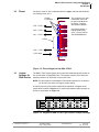
1
DNA/DNR-CT-651
Precision Timing Interface
Board
—
User Manual
January 2010 Edition
Version 1.0
PN Man-DNx-CT-651-0110
© Copyright 1998-2010 United Electronic Industries, Inc. All rights reserved.
No part of this publication may be reproduced, stored in a retrieval system, or transmitted, in any form
by any means, electronic, mechanical, by photocopying, recording, or otherwise without prior written
permission.
Information furnished in this manual is believed to be accurate and reliable. However, no responsibility
is assumed for its use, or for any infringements of patents or other rights of third parties that may result
from its use.
All product names listed are trademarks or trade names of their respective companies.
See UEI’s website for complete terms and conditions of sale:
http://www.ueidaq.com/company/terms.aspx
Contacting United Electronic Industries
Mailing Address:
27 Renmar Avenue
Walpole, MA 02081
U.S.A.
For a list of our distributors and partners in the US and around the world, please see
http://www.ueidaq.com/partners/
Support:
Telephone:
Fax:
(508) 921-4600
(508) 668-2350
Also see the FAQs and online “Live Help” feature on our web site.
Internet Support:
Support
Web-Site
FTP Site
[email protected]
www.ueidaq.com
ftp://ftp.ueidaq.com
Product Disclaimer:
WARNING!
DO NOT USE PRODUCTS SOLD BY UNITED ELECTRONIC INDUSTRIES, INC. AS CRITICAL
COMPONENTS IN LIFE SUPPORT DEVICES OR SYSTEMS.
Products sold by United Electronic Industries, Inc. are not authorized for use as critical components in
life support devices or systems. A critical component is any component of a life support device or
system whose failure to perform can be reasonably expected to cause the failure of the life support
device or system, or to affect its safety or effectiveness. Any attempt to purchase any United Electronic
Industries, Inc. product for that purpose is null and void and United Electronic Industries Inc. accepts
no liability whatsoever in contract, tort, or otherwise whether or not resulting from our or our
employees' negligence or failure to detect an improper purchase.
Note: Specifications shown in this document are subject to change without notice. Please check with
UEI for current status.
ii
iii
Table of Contents
Chapter 1 Introduction . . . . . . . . . . . . . . . . . . . . . . . . . . . . . . . . . . . . . . . . . . . . . . . . . . . . 1
1.1
Organization of this manual . . . . . . . . . . . . . . . . . . . . . . . . . . . . . . . . . . . . . . . . . . . . 1
1.2
DNx-CT-651 Precision Timing Interface Board Features . . . . . . . . . . . . . . . . . . . . . . 2
1.3
Photos. . . . . . . . . . . . . . . . . . . . . . . . . . . . . . . . . . . . . . . . . . . . . . . . . . . . . . . . . . . . . 2
1.4
DNx-CT-651 . . . . . . . . . . . . . . . . . . . . . . . . . . . . . . . . . . . . . . . . . . . . . . . . . . . . . . . . 2
1.5
1.5.1
1.5.2
Functional Description . . . . . . . . . . . . . . . . . . . . . . . . . . . . . . . . . . . . . . . . . . . . . . . . 3
Registers . . . . . . . . . . . . . . . . . . . . . . . . . . . . . . . . . . . . . . . . . . . . . . . . . . . . . 4
Operation . . . . . . . . . . . . . . . . . . . . . . . . . . . . . . . . . . . . . . . . . . . . . . . . . . . . . 4
1.6
Specifications . . . . . . . . . . . . . . . . . . . . . . . . . . . . . . . . . . . . . . . . . . . . . . . . . . . . . . . 5
1.7
Wiring and Connectors . . . . . . . . . . . . . . . . . . . . . . . . . . . . . . . . . . . . . . . . . . . . . . . . 5
1.8
Pinout . . . . . . . . . . . . . . . . . . . . . . . . . . . . . . . . . . . . . . . . . . . . . . . . . . . . . . . . . . . . . 6
1.9
Jumper Settings for DNA Version . . . . . . . . . . . . . . . . . . . . . . . . . . . . . . . . . . . . . . . . 6
Chapter 2 Programming with the High-Level API . . . . . . . . . . . . . . . . . . . . . . . . . . . . . . . 8
Chapter 3 Programming with the Low-Level API . . . . . . . . . . . . . . . . . . . . . . . . . . . . . . . 9
3.1
Data Representation . . . . . . . . . . . . . . . . . . . . . . . . . . . . . . . . . . . . . . . . . . . . . . . . . . 9
3.2
Configuration Settings. . . . . . . . . . . . . . . . . . . . . . . . . . . . . . . . . . . . . . . . . . . . . . . . . 9
3.3
Layer-specific Commands and Parameters . . . . . . . . . . . . . . . . . . . . . . . . . . . . . . . . 9
Index
. . . . . . . . . . . . . . . . . . . . . . . . . . . . . . . . . . . . . . . . . . . . . . . . . . . . . . . . . . . . . . . . . . 10
© Copyright 2010
United Electronic Industries, Inc.
Tel::508-921-4600
Date: January 2010
www.ueidaq.com
Vers: 1.0
DNx-CT-651-ManualTOC.fm
iv
List of Figures
Chapter 1 Introduction . . . . . . . . . . . . . . . . . . . . . . . . . . . . . . . . . . . . . . . . . . . . . . . . . . . . 1
1-1
DNA-and DNR-CT-651 Precision Timing Interface Boards ........................................... 2
1-2
Block Diagram of DNx-CT-651 Precision Timing Reference ......................................... 3
1-3
Pinout Diagram of the DNx-CT-651 ............................................................................... 6
1-4
Diagram of DNA-CT-651 Layer Position Jumper Settings............................................. 6
1-5
Physical Layout of DNA-CT-651 Layer Board ............................................................... 7
Chapter 2 Programming with the High-Level API . . . . . . . . . . . . . . . . . . . . . . . . . . . . . . . 8
(None)
Chapter 3 Programming with the Low-Level API . . . . . . . . . . . . . . . . . . . . . . . . . . . . . . . 9
(None)
© Copyright 2010
United Electronic Industries, Inc.
Tel::508-921-4600
Date: January 2010
www.ueidaq.com
Vers: 1.0
DNx-CT-651-ManualLOF.fm
DNx-CT-651 Precision Timing Interface Board
Chapter 1
Introduction
Chapter 1
Introduction
This document outlines the feature-set and operation of the UEI
DNA- and DNR-CT-651 Precision Timing Interface boards for use with UEI’s
Cube and RACKtangle data acquisition systems.
1.1
Organization This DNA-CT-651 User Manual is organized as follows:
of this manual
•
Chapter 1- Introduction
This section provides an overview of the document content, device
architecture, functional description, connectivity, and logic of the board.
•
Chapter 2 – Programming with the High Level API
This section explains how to program the CT-651 using the UEIDaq
Framework High Level API.
•
Chapter 3 – Programming with the Low Level API
This section describes how to program the CT-651 using the Low Level
API.
•
Appendix – A. Accessories
This appendix contains a list of associated equipment typically used with
the unit.
•
Index
This is an alphabetical listing of topics covered in this manual.
Manual Conventions
To help you get the most out of this manual and our products, please note that
we use the following conventions:
Tips are designed to highlight quick ways to get the job done, or reveal good
ideas you might not discover on your own.
NOTE: Notes alert you to important information.
CAUTION! Caution advises you of precautions to take to avoid
injury, data loss, and damage to your boards or a system crash.
Text formatted in bold typeface generally represents text that should be entered
verbatim. For instance, it can represent a command, as in the following
example: “You can instruct users how to run setup using a command such as
setup.exe.”
Frequently Asked Questions
For frequently answered questions, application notes, and support, visit us
online:
http://www.ueidaq.com/faq/
©
© CopyrightIndustries,
2010
January
all rights
28, 2010
reserved
Scheidt & Bach- Edit: TBD
Electronic
Inc.
Tel: 508-921-4600
www.ueidaq.com
Checked: TBD
www.ueidaq.com
Date:110
mann
UnitedUSA
Electronic Industries, Inc.
-821-2890
ScheidtDate:
& Bachmann
printed
January
January
2010 2010
651_Chap1.fm
Vers: Draft
Vers:
Vers:
1.0
1.0
Fax:
651_Chap1.fm
781-821-2891
1
DNx-CT-651 Precision Timing Interface Board
Chapter 1
Introduction
1.2
1.3
DNx-CT-651
Precision
Timing
Interface
Board
Features
The DNx-CT-651 Precision Timing Interface board s have the following features:
•
Provides 4 independent channels of synchronous 1 PPS timing signals
•
7 Operating Modes
— Input Follower.
— Input Follower w/ user-set pulse width.
— Auto-follower
— Auto- Follower w/ user-set pulse width.
— Free-run/Flywheel oscillator
— Sync_x Pass-through
— Disabled (OFF)
•
Fully software configurable
•
Standard ICD-GPS-060 output levels
•
Uses standard coaxial connectors
•
High accuracy / high stability on-board oscillator
•
UEI 10-year Availability Guarantee
Photos
DNA-CT-651
DNR-CT-651
Figure 1-1. DNA-and DNR-CT-651 Precision Timing Interface Boards
1.4
DNx-CT-651
The purpose of the DNx-CT-651 is to provide an industry-standard precision
timing interface for use with UEI Cube and RACKtangle Ethernet-based DAQ
systems to provide a wide variety of synchronization, timing reference, and
system heartbeat signals.
Each of four output channels may be set independently by software commands
from the host over the Ethernet port on the Cube or RACKtangle chassis to any
of the following configurations:
•
Slaved to the 1 PPS external input signal in “follower” modes
•
Same as above with user-set pulse width
•
Slaved to the 1 PPS external input signal in “auto-follower” mode
(switches to flywheel oscillator if input pulse is invalid)
•
Same as above with user-set pulse width
©
© CopyrightIndustries,
2010
January
all rights
28, 2010
reserved
Scheidt & Bach- Edit: TBD
Electronic
Inc.
Tel: 508-921-4600
www.ueidaq.com
Checked: TBD
www.ueidaq.com
Date:110
mann
UnitedUSA
Electronic Industries, Inc.
-821-2890
ScheidtDate:
& Bachmann
printed
January
January
2010 2010
651_Chap1.fm
Vers: Draft
Vers:
Vers:
1.0
1.0
Fax:
651_Chap1.fm
781-821-2891
2
DNx-CT-651 Precision Timing Interface Board
Chapter 1
Introduction
•
Free running (flywheel) 1 PPS output signal based on the on-board reference oscillator
•
Sync-x Pass-through of DNA Bus Signals to outputs
•
Disabled (OFF)
Two green LEDs are mounted on the front of the boards to indicate Power ON,
and Logic Active.
A functional block diagram of the CT-651 is illustrated in Figure 1-2 below.
Block Diagram:
Control
Logic
Switch
32-bit 66-MHz bus
DC/DC
Optical Isolation
I/O Connector
Frequency
Reference
Calibration
EEPROM
Figure 1-2. Block Diagram of DNx-CT-651 Precision Timing
Reference
1.5
Functional
Description
The 651 has four outputs, each of which can operate in any of five modes:
•
Input follower – accepts input pulses (10V) at a nominal rate of 1 pps
with a pulse width of 20 to 30 uS into a 50 ohm load and distributes them
to up to four outputs. This mode preserves the digital shape of the input
pulse and inserts minimal delay (skew) of 15-20 nS, but does not perform any validation of the input.
•
Input follower with user-set duty cycle – similar ti input follower mode
but has a user-defined duty cycle.
•
Input Auto-follower – output follows the external input signal until it
passes validation criteria. If the input becomes invalid, it switches automatically to the flywheel timing source, which adds a 30-40nS delay.
•
Input Auto- follower with user-set duty cycle – similar to input autofollower mode but has a user-defined duty cycle.
•
Flywheel oscillator – output is driven by an internal flywheel counter at
a user-settable rate (100/160 MHz) and duty cycle.
•
Pass-through – timing pulses from the Sync_x buses on the Cube or
RACKtangle chassis are passed through the CT-651 layer to its output
channels unchanged.
©
© CopyrightIndustries,
2010
January
all rights
28, 2010
reserved
Scheidt & Bach- Edit: TBD
Electronic
Inc.
Tel: 508-921-4600
www.ueidaq.com
Checked: TBD
www.ueidaq.com
Date:110
mann
UnitedUSA
Electronic Industries, Inc.
-821-2890
ScheidtDate:
& Bachmann
printed
January
January
2010 2010
651_Chap1.fm
Vers: Draft
Vers:
Vers:
1.0
1.0
Fax:
651_Chap1.fm
781-821-2891
3
DNx-CT-651 Precision Timing Interface Board
Chapter 1
Introduction
•
1.5.1
1.5.2
Registers
Operation
Disabled (OFF)
The 651 uses the following registers:
•
LCR – Layer Control Register
As the name implies, this register controls the layer.
•
FWCFG – Output Mode Config Register
This register selects the operating mode and sub-modes for each channel, such as input follow and input auto-follow operation
•
DW – DAC Write Register
This register sets the hysteresis of input signal monitoring and also
adjusts the internal 20 MHz reference clock as needed. It also controls
all write and operating functions of the DACs.
•
FWDC – Flywheel Duty Cycle Register
This register sets the duty cycle of the flywheel counter pulse
•
FWDIV – Flywheel Output Period Register
This register sets the total period of the flywheel counter pulse
•
FWCLK_MIN – Flywheel Clock Divider Auto-correction Low Limit
This register sets the low limit for monitoring flywheel period.
•
FWCLK_MAX – Flywheel Clock Divider Auto-correction High Limit
This register sets the high limit for monitoring flywheel period.
•
FWCRH – Input clock “High” count in 100/160 MHz ticks
•
FWCRP – Input clock “Period” count in 100/160 MHz ticks
•
STS – General Status Register
indicates when input clock fails validation and when a DAC write is in
progress.
The general sequence of operation at startup is as follows:
1. Using the DqAdvSetRegister( ) function, write to the LCR. This will enable
the DC/DC converter for power, select 100 or 160 MHz internal flywheel
clock rate “clock_fw”, and if desired, enable the 50-ohm cable termination.
2. Use the DqAdv SetRegister ( ) function to set the following registers:
– FWCFG output mode selection
– DW to adjust hysteresis for input pulse conditioning
– FWDC to control flywheel clock duty cycle
– FWDIV to control flywheel clock period
– FWCLK_MIN to set the FW clock divider auto-correction low limit
– FWCLK_MIN to set the FW clock divider auto-correction high limit
3. The DqAdv GetRegister ( ) function may be used to check the contents or
status of any of the readable registers (R) or (W) listed above.
NOTE: For a more detailed description of functional operation, refer to the API
User Manual.
©
© CopyrightIndustries,
2010
January
all rights
28, 2010
reserved
Scheidt & Bach- Edit: TBD
Electronic
Inc.
Tel: 508-921-4600
www.ueidaq.com
Checked: TBD
www.ueidaq.com
Date:110
mann
UnitedUSA
Electronic Industries, Inc.
-821-2890
ScheidtDate:
& Bachmann
printed
January
January
2010 2010
651_Chap1.fm
Vers: Draft
Vers:
Vers:
1.0
1.0
Fax:
651_Chap1.fm
781-821-2891
4
DNx-CT-651 Precision Timing Interface Board
Chapter 1
Introduction
1.6
Specifications
The following table lists the technical specifications of the CT-651 board.
Technical Specifications:
Outputs
Output channels
Output selection
Output Signal Levels
Output High
Output Low
Output Clamping
Output chan to chan skew
Output Signal Dynamics
Output Rise Time
Output Fall Time
Output Pulse Width
4
7 modes:
1 PPS input follower; Follower w/ user-set pulse
width; Auto follower w/auto switch to flywheel;
Auto follower w/ switch to flywheel and w/
user-set pulse width; 1PPS flywheel oscillator;
Sync-x pass-through; Disabled (off )
Conform to ICD-GPS-060
+10 VDC, +2/-1 VDC (@ 50 Ω)
0 VDC, +2/-1 VDC (@ 50 Ω)
Output not to exceed 13 VDC regardless of load
impedance
2.5 nS max
Conform to ICD-GPS-060 (Rv B, Fig 3-2)
< 50 nS (10% to 90%)
< 1 μS (90% to 10%)
20 μS typical (16 μS min, 30 μS max)
Sync Input
Input Range
Input Impedance
Switch Threshold
Sync Input to Output skew
0 - 10 VDC (-2 VDC min, +20 VDC max)
50 Ω ±10% or >10 kΩ (SW selectable)
2.5 VDC ±5% (SW programmable between
0.5VDC and 9.5 VDC)
35 nS max (@ 2.5 VDC)
Flywheel Oscillator
Output Frequency
Initial Accuracy
Output Stability
Connector
On-board connector
Mating connector
1 PPS
±1 PPM
300 parts per billion per day
(D-sub style with 5 coaxial connections)
Conec 3017W5SCT78N40X or equiv
Conec 3017W5PXK99A10X or equiv
General
Power dissipation
Operating Temp. Range
Operating Humidity
Vibration IEC 60068-2-6
IEC 60068-2-64
Shock IEC 60068-2-27
MTBF
Testing Conditions
1.7
Wiring and
Connectors
<3W
Tested -40 to +85 °C
95%, non-condensing
5 g, 10-500 Hz, sinusoidal
5 g (rms), 10-500 Hz, broad-band random
50 g, 3 ms half sine, 18 shocks @ 6 orientations
30 g, 11 ms half sine, 18 shocks @ 6 orientations
300,000 hours
All testing assumes 50 Ω terminations at 150
foot coaxial cable unless otherwise noted
All external connections to the CT-651 are made through the front-accessible
D-sub combination male connector. This connector has five coaxial connectors
and 12 pins. The mating female connector (supplied by user) is a standard
Conec Type 3017W5PXK99A10X or equivalent, which is widely available from a
number of suppliers.
©
© CopyrightIndustries,
2010
January
all rights
28, 2010
reserved
Scheidt & Bach- Edit: TBD
Electronic
Inc.
Tel: 508-921-4600
www.ueidaq.com
Checked: TBD
www.ueidaq.com
Date:110
mann
UnitedUSA
Electronic Industries, Inc.
-821-2890
ScheidtDate:
& Bachmann
printed
January
January
2010 2010
651_Chap1.fm
Vers: Draft
Vers:
Vers:
1.0
1.0
Fax:
651_Chap1.fm
781-821-2891
5
DNx-CT-651 Precision Timing Interface Board
Chapter 1
Introduction
1.8
Pinout
The pinout of the CT-651 is illustrated below in Figure 1-3. Note that channels
are numbered from 0 to 3.
Coaxial
Connectors
Ch3 - 1 PPS
Ch2 - 1 PPS
Ch1 - 1 PPS
12 Pins
User should supply a
mating female connector -- Conec Part No.
3017W5PXK99A10X
Ch0 - 1 PPS
1 PPS Input
This connector is a male
combination coax and
pin type manufactured
by Conec -- Part No.
3017W5SCT78N40X.
"
C,HD
Figure 1-3. Pinout Diagram of the DNx-CT-651
1.9
Jumper
Settings for
DNA Version
The DNA-CT-651 module (layer) has a jumper block that assigns the position of
the module within a PowerDNA Cube. The jumpers must be set to match the
physical position of an I/O board or layer in the Cube.
NOTE: Since all layers are assembled in Cubes before shipment to a customer,
you should never have to change a jumper setting.
In case a jumper may have been inadvertently misplaced, a diagram of the
jumper block is shown in Figure 1-4. To set the layer address, place jumpers as
shown for I/O position 1in Figure 1-4.
Jx Pins
I/O 1
Layer’s Position as marked on the Faceplate*
I/O 2
I/O 3
I/O 4
I/O 5
I/O 6
9-10
11-12
13-14
15-16
* All I/O Layers are sequentially enumerated from top to the bottom of the Cube
- Open
- Closed
Figure 1-4. Diagram of DNA-CT-651 Layer Position Jumper Settings
©
© CopyrightIndustries,
2010
January
all rights
28, 2010
reserved
Scheidt & Bach- Edit: TBD
Electronic
Inc.
Tel: 508-921-4600
www.ueidaq.com
Checked: TBD
www.ueidaq.com
Date:110
mann
UnitedUSA
Electronic Industries, Inc.
-821-2890
ScheidtDate:
& Bachmann
printed
January
January
2010 2010
651_Chap1.fm
Vers: Draft
Vers:
Vers:
1.0
1.0
Fax:
651_Chap1.fm
781-821-2891
6
DNx-CT-651 Precision Timing Interface Board
Chapter 1
Introduction
DNA 120-pin Bus Connector
4
2
5
7
9
11
15
13
16
14
J1
3
1
6
8
10
12
See Figure 1-4 for
jumper locations for
setting layer position.
DB-62 I/O Connector
External Circuits
Figure 1-5. Physical Layout of DNA-CT-651 Layer Board
©
© CopyrightIndustries,
2010
January
all rights
28, 2010
reserved
Scheidt & Bach- Edit: TBD
Electronic
Inc.
Tel: 508-921-4600
www.ueidaq.com
Checked: TBD
www.ueidaq.com
Date:110
mann
UnitedUSA
Electronic Industries, Inc.
-821-2890
ScheidtDate:
& Bachmann
printed
January
January
2010 2010
651_Chap1.fm
Vers: Draft
Vers:
Vers:
1.0
1.0
Fax:
651_Chap1.fm
781-821-2891
7
DNx-CT-651 Precision Timing Interface Board
Chapter 2
Programming with the High-Level API
Chapter 2
Programming with the High-Level API
No Framework support for the CT-651 is currently available. Although it will be
provided in the near future, the schedule has not yet been determined. Check
with UEI periodically for current status.
©
© CopyrightIndustries,
2010
January
all rights
28, 2010
reserved
Scheidt & Bach- Edit: TBD
Electronic
Inc.
Tel: 508-921-4600
www.ueidaq.com
Checked: TBD
www.ueidaq.com
Date:110
mann
UnitedUSA
Electronic Industries, Inc.
-821-2890
ScheidtDate:
& Bachmann
printed
January
January
2010 2010
651_ Chap2.fm
Vers: Draft
Vers:
Vers:
1.0
1.0
Fax:
651_
781-821-2891
Chap2.fm
8
DNx-CT-651 Precision Timing Interface Board
Chapter 3
Programming with the Low-Level API
Chapter 3
Programming with the Low-Level API
This section describes how to program the PowerDNA cube using the low-level
API. The low-level API offers direct access to PowerDNA DAQBios protocol and
also allows you to directly access device registers.
We recommend that you use UeiDaq High-level Framework (see Chapter 2),
when it is available, because it is easier to use than the low-level API.
You should only need to use the low-level API if you are using an operating
system other than Windows.
3.1
Data
Representation
3.2
Configuration Configuration settings are passed in using the DqAdv651SetRegister function
described below.
Settings
Register data is represented as 32-bit words, unless otherwise specified.
The following bits are used:
#define DQ_LN_ACTIVE
#define DQ_LN_DCEN
(1L<<1)
// “STS” LED status
(1L<<0)
// enable operations
DQ_LN_ACTIVE flag is needed to switch on “STS” LED on CPU layer.
DQ_LN_DCEN flag enables DC power and all operations with the layer
3.3
Layer-specific The CT-651 layer API provides two functions that directly access configuration
registers. See register definition for details. See the PowerDNA API Reference
Commands
Manual for a complete description of these functions.
and
• DqAdv651SetRegister()
Parameters
This function writes value to the selected reg register. reg specifies
the register of interest.
•
DqAdv651GetRegister()
This function reads value from the selected reg register. reg specifies
the register of interest.
©
© CopyrightIndustries,
2010
January
all rights
28, 2010
reserved
Scheidt & Bach- Edit: TBD
Electronic
Inc.
Tel: 508-921-4600
www.ueidaq.com
Checked: TBD
www.ueidaq.com
Date:110
mann
UnitedUSA
Electronic Industries, Inc.
-821-2890
ScheidtDate:
& Bachmann
printed
January
January
2010 2010
651_Chap3.fm
Vers: Draft
Vers:
Vers:
1.0
1.0
Fax:
651_Chap3.fm
781-821-2891
9
10
Index
B
Block Diagram
I
3
Input Auto-follower 3
Input follower 3
Inserting the Mni Card
C
Channel List Settings 9
Configuration Settings 9
Conventions 1
J
Jumper Settings
D
Data Representation 9
Disabled 4
DNx-CT-65 2
DW – DAC Write Register
6
L
Layer position jumper settings 6
Layer-specific Commands 9
LCR – Layer Control Register 4
Low-Level API 9
4
F
Features 2
Flywheel oscillator 3
Functional Description 2, 3
FWCFG – Output Mode Config Register 4
FWCLK_MIN – Flywheel Clock Divider Auto-correction Low Limit 4
FWCNT – Current value of flywheel counter, 4
FWCRH – Input clock “High” count in 100/160 MHz
ticks 4
FWCRP – Input clock “Period” count in 100/160
MHz ticks 4
FWDC – Flywheel Duty Cycle Registe 4
FWDIV – Flywheel Output Period Register 4
H
O
Operation 4
Organization
1
P
Pass-through 4
Photos 2
Physical layout 7
R
Registers
4
S
Specifications 5
STS – General Status Register
4
W
High-Level API 8
© Copyright 2009
United Electronic Industries, Inc.
6
WCLK_MAX – Flywheel Clock Divider Auto-correction High Limit 4
Wiring 5
Tel: 508-921-4600
Date: January 2010
www.ueidaq.com
Vers: 1.0
File: DNx-CT-651-ManualIX.fm