1
Z16C30
USC
User’s Manual
UM009402-0201
ZiLOG Worldwide Headquarters • 910 E. Hamilton Avenue • Campbell, CA 95008
Telephone: 408.558.8500 • Fax: 408.558.8300 • www.ZiLOG.com
Z16C30
USC
This publication is subject to replacement by a later edition. To determine whether a later
edition exists, or to request copies of publications, contact:
ZiLOG Worldwide Headquarters
910 E. Hamilton Avenue
Campbell, CA 95008
Telephone: 408.558.8500
Fax: 408.558.8300
www.ZiLOG.com
Document Disclaimer
ZiLOG is a registered trademark of ZiLOG Inc. in the United States and in other countries. All other products
and/or service names mentioned herein may be trademarks of the companies with which they are associated.
©2001 by ZiLOG, Inc. All rights reserved. Information in this publication concerning the devices,
applications, or technology described is intended to suggest possible uses and may be superseded. ZiLOG,
INC. DOES NOT ASSUME LIABILITY FOR OR PROVIDE A REPRESENTATION OF ACCURACY OF
THE INFORMATION, DEVICES, OR TECHNOLOGY DESCRIBED IN THIS DOCUMENT. ZiLOG
ALSO DOES NOT ASSUME LIABILITY FOR INTELLECTUAL PROPERTY INFRINGEMENT
RELATED IN ANY MANNER TO USE OF INFORMATION, DEVICES, OR TECHNOLOGY
DESCRIBED HEREIN OR OTHERWISE. Except with the express written approval of ZiLOG, use of
information, devices, or technology as critical components of life support systems is not authorized. No
licenses are conveyed, implicitly or otherwise, by this document under any intellectual property rights.
UM009402-0201
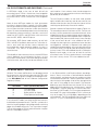
Z16C30 USC® USER'S MANUAL
SUPPLEMENTARY INFORMATION
ZILOG
Z16C30 USC® USER'S MANUAL
Thank you for your interest in Zilog's high-speed Integrated Universal Serial Controller.
To aid the designer, the following support material is available when designing
a High Performance Serial Communication application based on Zilog's USC.
Z16C30 User's Manual
Zilog's USC® User's Manual is a comprehensive breakdown of the functions and features of the USC which will
aid in the development of your application. A good place
to start is the Overview section at the beginning of the
manual, which provides a short description of each feature
and chapter. Then any chapter can be reviewed in more
detail as necessary. This User's Manual provides in-depth
descriptions of all functions and features of the USC as well
as supporting block diagrams, timing diagrams, and sample
applications.
Z16C30 Product Specification
The USC® Product Specification is a good resource to help
determine which of Zilog's High Performance Serial Controllers to use. This document provides an in-depth description of the USC, including descriptions of features,
block diagrams, pin assignments, pin descriptions, register bit functions, and AC and DC specifications. This
specification can be found in the High Speed Serial Communication Controllers Databook, DC-8314-01, which also
includes a product specification on the Z16C30 USC as
well as related Application Notes, support products, and a
list of third party support vendors.
Application Notes
The following Application Notes are useful in demonstrating how the USC can be used in different applications.
Design a Serial Board to Handle Multiple Protocols
This Application Note details an approach to handling
multiple serial communication protocols using Zilog's
Z16C30 USC. This document is included in the High
Speed SCC Databook, DC-8314-01 mentioned above.
The Zilog Datacom Family with the 80186 CPU
This Application Note, DC-2560-03, explains and illustrates how Zilog's datacom family interfaces and communicates with the 80186 on an evaluation board.
Demonstration/Evaluation Boards
By selecting the board that most closely resembles your
desired application, you may be able to use parts of the
design in your implementation. These boards can be used
as software platforms while the application hardware is
being developed.
Z8018600ZCO - This kit contains an assembled circuit
board, software, and documentation to support the evaluation and development of code for Zilog's Z16C30 USC,
Z16C32 IUSC, Z85C30 SCC, Z85230 ESCC, and Z16C35
UM97USC0100
ISCC. The purpose of the board is to illustrate how the
datacom family interfaces and communicates with the
80186 CPU. This will help potential customers evaluate
Zilog's datacommunications with the 80186 CPU. A boardresident monitor program allows code to be downloaded
and executed. A specification on this product is included
in the High Speed Serial Communication Controllers
Databook, DC-8314-01 mentioned above.
UM009402-0201
Z16C30 USC® U SER'S MANUAL
SUPPLEMENTARY INFORMATION
ZILOG
Demonstration/Evaluation Boards (Continued)
Z16C3001ZCO - This kit contains an assembled PC/XT/AT
circuit board with two high-speed serial connections, DB9
and DB25 connectors selectively driven by RS-232 or
RS422 line drivers.
The board illustrates the use of Zilog's USC in communications applications such as ASYNC, SDLC/HDLC and highspeed ASYNC. (Please refer to the Product Specification
Databook for a detailed description.)
The kit also contains software and documentation to support software and hardware development for Zilog's USC.
© 1997 by Zilog, Inc. All rights reserved. No part of this document
may be copied or reproduced in any form or by any means
without the prior written consent of Zilog, Inc. The information in
this document is subject to change without notice. Devices sold
by Zilog, Inc. are covered by warranty and patent indemnification
provisions appearing in Zilog, Inc. Terms and Conditions of Sale
only. Zilog, Inc. makes no warranty, express, statutory, implied or
by description, regarding the information set forth herein or
regarding the freedom of the described devices from intellectual
property infringement. Zilog, Inc. makes no warranty of merchantability or fitness for any purpose. Zilog, Inc. shall not be
responsible for any errors that may appear in this document.
Zilog, Inc. makes no commitment to update or keep current the
information contained in this document.
Zilog’s products are not authorized for use as critical components in life support devices or systems unless a specific written
agreement pertaining to such intended use is executed between
the customer and Zilog prior to use. Life support devices or
systems are those which are intended for surgical implantation
into the body, or which sustains life whose failure to perform,
when properly used in accordance with instructions for use
provided in the labeling, can be reasonably expected to result in
significant injury to the user.
Zilog, Inc. 210 East Hacienda Ave.
Campbell, CA 95008-6600
Telephone (408) 370-8000
Telex 910-338-7621
FAX 408 370-8056
Internet: http://www.zilog.com
UM009402-0201
UM97USC0100
Z16C30 USC®
USER'S MANUAL
ZILOG
Z16C30 USC® USER'S MANUAL
TABLE OF CONTENTS
CHAPTER TITLE AND SUBSECTIONS
PAGE
Chapter 1 Introduction
1.1
Introduction ....................................................................................................... 1-1
1.2
Features ............................................................................................................. 1-1
1.3
Logic Symbol ..................................................................................................... 1-2
1.4
Packaging ......................................................................................................... 1-3
1.5
Overview of the USC and this Manual ............................................................... 1-4
1.5.1 Bus Interfacing ....................................................................................... 1-4
1.5.2 Serial Interfacing ..................................................................................... 1-4
1.5.3 Serial Modes and Protocols .................................................................... 1-4
1.5.4 DMA Operation ....................................................................................... 1-4
1.5.5 Interrupts ................................................................................................ 1-4
1.5.6 Software Summary .................................................................................. 1-4
1.6
Device Structure .............................................................................................. 1-12
1.6.1 The Transmit Data Path ........................................................................ 1-12
1.6.2 The Receive Data Path ......................................................................... 1-12
1.6.3 Clocking ................................................................................................ 1-12
1.6.4 Interrupts .............................................................................................. 1-12
1.7
Document Structure ........................................................................................ 1-13
Chapter 2 Bus Interfacing
2.1
Introduction ....................................................................................................... 2-1
2.2
Multiplexed/Non-Multiplexed Operation ............................................................ 2-1
2.3
Read/Write Data Strobes ................................................................................... 2-3
2.4
Bus Width .......................................................................................................... 2-4
2.5
ACK vs. WAIT Handshaking .............................................................................. 2-4
2.6
Pin Descriptions ................................................................................................ 2-5
2.7
Pull-up Resistors and Unused Pins ................................................................... 2-7
2.8
The Bus Configuration Register (BCR) .............................................................. 2-7
2.8.1 WAIT vs. Ready Selection ...................................................................... 2-7
2.8.2 Bits and Fields in the BCR ...................................................................... 2-7
2.9
Register Addressing .......................................................................................... 2-8
2.9.1 Implicit Data Register Addressing .......................................................... 2-8
2.9.2 Direct Register Addressing on AD13-AD8 ............................................. 2-8
2.9.3 Direct Register Addressing on AD6-AD0/7-1 ......................................... 2-9
2.9.4 Indirect Register Addressing in the CCAR ............................................. 2-9
2.9.5 About the Register Address Tables ..................................................... 2-10
2.9.6 Serial Data Registers TDR & RDR ........................................................ 2-14
2.9.7 Byte Ordering ....................................................................................... 2-14
2.9.8 Register Read & Write Cycles .............................................................. 2-14
UM97USC0100
i
UM009402-0201
Z16C30 USC®
USER'S MANUAL
ZILOG
CHAPTER TITLE AND SUBSECTIONS
PAGE
Chapter 3 A Sample Introduction
3.1
Introduction ....................................................................................................... 3-1
Chapter 4 Serial Interfacing
4.1
Introduction ....................................................................................................... 4-1
4.2
Serial Interface Pin Descriptions ....................................................................... 4-1
4.3
Transmit and Receive Clocking ........................................................................ 4-2
4.3.1 CTR0 and CTR1 ...................................................................................... 4-2
4.3.2 The Baud Rate Generators ..................................................................... 4-2
4.3.3 Introduction to the DPLL ......................................................................... 4-5
4.3.4 TxCLK and RxCLK Selection .................................................................. 4-5
4.3.5 Clocking for Asynchronous Mode .......................................................... 4-6
4.3.6 Synchronous Clocking ............................................................................ 4-6
4.3.7 Stopping the Clocks ............................................................................... 4-6
4.4
Data Formats and Encoding ............................................................................. 4-7
4.5
More About the DPLL ........................................................................................ 4-8
4.6
The RxD and TxD Pins .................................................................................... 4-10
4.7
Edge Detection and Interrupts ........................................................................ 4-11
4.8
The /DCD Pin ................................................................................................... 4-13
4.9
The /CTS Pin .................................................................................................... 4-15
4.10 The /RxC and /TxC Pins .................................................................................. 4-16
4.11 The /RxReq and /TxReq Pins .......................................................................... 4-17
4.12 The /RxACK and /TxACK Pins ......................................................................... 4-17
Chapter 5 Serial Modes and Protocols
5.1
Introduction ....................................................................................................... 5-1
5.2
Asynchronous Modes ........................................................................................ 5-1
5.3
Character Oriented Synchronous Modes .......................................................... 5-3
5.4
Bit Oriented Synchronous Modes ..................................................................... 5-4
5.5
The Mode Registers (CMR,TMR & RMR) .......................................................... 5-5
5.5.1 Enabling and Disabling the Receiver and Transmitter ........................... 5-7
5.5.2 Character Length .................................................................................... 5-7
5.5.3 Parity, CRC, Serial Encoding .................................................................. 5-8
5.6
Asynchronous Mode ......................................................................................... 5-9
5.6.1 Break Conditions .................................................................................. 5-10
5.7
Isochronous Mode ........................................................................................... 5-10
5.8
Nine-Bit Mode .................................................................................................. 5-11
5.9
External Sync Mode ........................................................................................ 5-12
5.10 Monosync and Bisync Modes ......................................................................... 5-12
5.11 Transparent Bisync Mode ............................................................................... 5-14
5.12 Slaved Monosync Mode .................................................................................. 5-15
5.13 IEEE 802.3 (Ethernet) Mode ............................................................................ 5-16
5.14 HDLC/SDLC Mode .......................................................................................... 5-18
5.14.1 Received Address and Control Field Handling .................................... 5-18
5.14.2 Frame Length Residuals ....................................................................... 5-20
5.14.3 Handling a Received Abort .................................................................. 5-20
UM009402-0201
ii
UM97USC0100
Z16C30 USC®
USER'S MANUAL
ZILOG
CHAPTER TITLE AND SUBSECTIONS
5.15
5.16
5.17
5.18
5.19
5.20
5.21
5.22
5.23
5.24
5.25
PAGE
HDLC/SDLC Loop Mode ................................................................................. 5-21
Cyclic Redundancy Checking ......................................................................... 5-22
Parity Checking ............................................................................................... 5-25
Status Reporting .............................................................................................. 5-26
5.18.1 Detailed Status in the TCSR ................................................................. 5-28
5.18.2 Detailed Status in the RCSR ................................................................. 5-29
DMA Support Features .................................................................................... 5-31
5.19.1 The Character Counters ....................................................................... 5-31
5.19.2 The RCC FIFO ...................................................................................... 5-35
5.19.3 Transmit Control Blocks ........................................................................ 5-36
5.19.4 Receive Status Blocks .......................................................................... 5-38
5.19.5 Finding the End of a Received Frame .................................................. 5-39
Commands ...................................................................................................... 5-40
Resetting a USC Channel ................................................................................ 5-44
The Data Registers and the FIFO's ................................................................. 5-45
5.22.1 Accessing the TDR & RDR ................................................................... 5-45
5.22.2 TxFIFO and RxFIFO Operation ............................................................. 5-45
5.22.3 Fill Levels .............................................................................................. 5-46
5.22.4 DMA & Interrupt Request Levels .......................................................... 5-46
Handling Overruns & Underruns ..................................................................... 5-47
5.23.1 Tx Underruns ........................................................................................ 5-47
5.23.2 Rx Overruns .......................................................................................... 5-47
5.23.3 Rx Overrun Scribbling .......................................................................... 5-48
5.23.4 Fill Level Correctness & Extra Bytes ..................................................... 5-48
Between Frames, Messages, or Characters ................................................... 5-49
5.24.1 Synchronous Transmission ................................................................... 5-49
5.24.2 Async Transmission .............................................................................. 5-49
5.24.3 Synchronous Reception ....................................................................... 5-51
Synchronizing Frames/Messages with Software Response ............................ 5-51
Chapter 6 Direct Memory Access (DMA) Interfacing
6.1
Introduction ....................................................................................................... 6-1
6.2
Flyby vs. Flowthrough DMA Operation .............................................................. 6-1
6.3
DMA Requests by the Receiver & Transmitter .................................................. 6-6
6.3.1 Programming the DMA Request Levels ................................................. 6-7
6.4
DMA Acknowledge Signals ............................................................................... 6-8
6.5
Separating Received Frames in Memory .......................................................... 6-8
UM97USC0100
iii
UM009402-0201
Z16C30 USC®
USER'S MANUAL
ZILOG
CHAPTER TITLE AND SUBSECTIONS
PAGE
Chapter 7 Interrupts
7.1
Introduction ....................................................................................................... 7-1
7.2
Interrupt Acknowledge Daisy-Chains ................................................................ 7-1
7.3
External Interrupt Control Logic ........................................................................ 7-2
7.4
Using /RxReq and /TxReq as Interrupt Requests ............................................. 7-3
7.5
Interrupt Types & Sources ................................................................................. 7-4
7.6
Internal Interrupt Operation ............................................................................... 7-6
7.7
Details of the Model ........................................................................................... 7-8
7.8
Interrupt Option in the BCR ............................................................................... 7-9
7.9
Interrupt Acknowledge Cycles .......................................................................... 7-9
7.10 Interrupt Acknowledge vs. Read Cycles ......................................................... 7-14
7.11 Interrupt Types ................................................................................................ 7-14
7.11.1 Receive Status Interrupt Sources and IA Bits ...................................... 7-14
7.11.2 Receive Data Interrupts ........................................................................ 7-15
7.11.3 Transmit Status Interrupt Sources and IA Bits ...................................... 7-18
7.11.4 Transmit Data Interrupts ....................................................................... 7-19
7.11.5 I/O Pin Interrupt Sources and IA Bits .................................................... 7-20
7.11.6 Miscellaneous Interrupt Sources and IA Bits ....................................... 7-20
7.12 Interrupt Pending and Under Service Bits ...................................................... 7-21
7.13 Interrupt Enable Bits ........................................................................................ 7-22
7.14 Channel Interrupt Options ............................................................................... 7-22
7.15 Interrupt Vectors .............................................................................................. 7-23
7.16 Software Requirements ................................................................................... 7-24
7.16.1 Nested Interrupts .................................................................................. 7-24
7.16.2 Which Type(s) to Handle? .................................................................... 7-24
7.16.3 Handling a Type ................................................................................... 7-25
7.16.4 Exiting the ISR ...................................................................................... 7-27
Chapter 8 Software Summary
8.1
Introduction ....................................................................................................... 8-1
8.2
About Resetting ................................................................................................. 8-1
8.3
Programming Order .......................................................................................... 8-2
8.4
Using DMA to Initialize a Channel ..................................................................... 8-2
8.5
Determining the Device Revision Level ............................................................. 8-3
8.6
Tips & Techniques ............................................................................................. 8-3
8.6.1 Common Hardware Problems ................................................................ 8-3
8.6.2 Common Software Problems .................................................................. 8-3
8.7
Test Modes ........................................................................................................ 8-6
8.8
Register Reference .......................................................................................... 8-10
8.8.1 Register Addresses .............................................................................. 8-10
8.8.2 Conditions/Context ............................................................................... 8-10
8.8.3 Description ........................................................................................... 8-10
8.8.4 RW Status ............................................................................................. 8-10
UM009402-0201
iv
UM97USC0100
Z16C30 USC®
USER'S MANUAL
ZILOG
CHAPTER TITLE AND SUBSECTIONS
PAGE
Appendix A Appendix Changes
A.1 Introduction ............................................................................................................ A-1
A.1.1 Transmit Status Blocks/Transmit Control Blocks .................................... A-1
A.1.2 Interrupt Enable (for Individual Sources) Interrupt Arm ......................... A-1
A.2
Commands ........................................................................................................ A-1
A.2.1 Reload RCC/TCC
Load RCC/TCC ....................................................................................... A-1
A.2.2 Select Straight/Swapped Memory .......................................................... A-1
A.2.3 Preset CRC Clear Tx/Rx CRC Generator ................................................ A-1
A.3
Bit/Field Names ................................................................................................. A-1
Appendix B
Questions and Answers ............................................................................................... B-1
UM97USC0100
v
UM009402-0201
Z16C30 USC®
USER'S MANUAL
ZILOG
FIGURE TITLES
PAGE
Chapter 1
Figure 1-1.
Figure 1-2.
Figure 1-3.
USC Logic Symbol ................................................................................. 1-2
USC 68-pin PLCC Pinout ........................................................................ 1-3
USC Block Diagram .............................................................................. 1-11
Chapter 2
Figure 2-1.
Figure 2-2.
Figure 2-3.
Figure 2-4.
Figure 2-5.
Figure 2-6.
Figure 2-7.
Figure 2-8.
Figure 2-9.
Figure 2-10.
Figure 2-11.
Figure 2-12.
Figure 2-13.
Simple Multiplexed System .................................................................... 2-1
Simple Interface to Non-Multiplexed Bus ............................................... 2-2
User-Friendly Interface to Non-Multiplexed Bus .................................... 2-2
/RD & /WR Signaling ............................................................................... 2-3
R//W and /DS Signaling .......................................................................... 2-3
A Fast and Slow Cycle with Three Kinds of Handshaking ..................... 2-5
The USC's Bus Configuration Register (BCR) ........................................ 2-7
The Channel Command/Address Register (CCAR) ............................. 2-10
USC Register Addressing .................................................................... 2-11
A Register Read Cycle with Multiplexed Addresses and Data ............ 2-15
A Register Write Cycle with Multiplexed Addresses and Data ............ 2-16
A Register Read Cycle with Non-Multiplexed Data Lines .................... 2-17
A Register Write Cycle with Non-Multiplexed Data Lines ..................... 2-18
Chapter 3
Figure 3-1.
Figure 3-2.
Sample Application ................................................................................ 3-2
Serial Interface for Sample Application .................................................. 3-3
Chapter 4
Figure 4-1.
Figure 4-2.
Figure 4-3.
Figure 4-4.
Figure 4-5.
Figure 4-6.
Figure 4-7.
Figure 4-8.
Figure 4-9.
Figure 4-10.
A Model of a USC Channel's Clocking Logic ......................................... 4-3
The Clock Mode Control Register (CMCR) ............................................ 4-4
The Hardware Configuration Register (HCR) ......................................... 4-4
Data Formats/Encoding .......................................................................... 4-7
The Channel Command/Status Register (CCSR) ................................... 4-9
The Input/Output Control Register (IOCR) ........................................... 4-10
The Status Interrupt Control Register (SICR) ........................................ 4-12
The Miscellaneous Interrupt Status Register (MISR) ............................ 4-12
/DCD Auto-Enable Timing .................................................................... 4-14
/CTS Auto-Enable Timing ..................................................................... 4-15
UM009402-0201
vi
UM97USC0100
Z16C30 USC®
USER'S MANUAL
ZILOG
FIGURE TITLES
PAGE
Chapter 5
Figure 5-1.
Figure 5-2.
Figure 5-3.
Figure 5-4.
Figure 5-5.
Figure 5-6.
Figure 5-7.
Figure 5-8.
Figure 5-9.
Figure 5-10.
Figure 5-11.
Figure 5-12.
Figure 5-13.
Figure 5-14.
Figure 5-15.
Figure 5-16.
Figure 5-17.
Figure 5-18.
Figure 5-19.
Asynchronous Data ................................................................................ 5-2
Character Oriented Synchronous Data .................................................. 5-2
HDLC/SDLC Data ................................................................................... 5-4
The Channel Mode Register (CMR) ....................................................... 5-6
The Transmit Mode Register (TMR) ........................................................ 5-6
The Receive Mode Register (RMR) ........................................................ 5-6
Carrier Detection for a Received Ethernet Frame ................................ 5-16
The Channel Command/Status Register (CCSR) ................................. 5-21
A Model of the Receive Datapath ......................................................... 5-24
How a USC Channel Provides the "Queued" Status Bits in the RCSR. 5-27
The Transmit Command/Status Register (TCSR) ................................. 5-28
The Receive Command/Status Register (RCSR) .................................. 5-29
A Model of the Transmit Character Counter Feature ............................ 5-33
A Model of the Receive Character Counter Feature ............................ 5-34
The Channel Command/Status Register (CCSR) ................................. 5-37
The Channel Control Register (CCR) ................................................... 5-37
A 32-Bit Transmit Control Block in a DMA Buffer ................................. 5-37
A 32-Bit Receive Status Block in a DMA Buffer .................................... 5-38
The Channel Command/Address Register (CCAR) ............................. 5-41
Chapter 6
Figure 6-1.
Figure 6-2.
Figure 6-3.
Figure 6-4.
Flowthrough DMA Transfer Memory to Peripheral Device ..................... 6-2
Flowthrough DMA Transfer, Peripheral Device to Memory .................... 6-3
Flyby DMA Transfer, Memory to Peripheral Device ............................... 6-4
*Flyby DMA Transfer, Peripheral Device to Memory .............................. 6-5
UM97USC0100
vii
UM009402-0201
Z16C30 USC®
USER'S MANUAL
ZILOG
FIGURE TITLES
Chapter 7
Figure 7-1.
Figure 7-2.
Figure 7-3.
Figure 7-4.
Figure 7-5.
Figure 7-6.
Figure 7-7.
Figure 7-8.
Figure 7-9.
Figure 7-10.
Figure 7-11.
Figure 7-12.
Figure 7-13.
Figure 7-14.
Figure 7-15.
Figure 7-16.
Figure 7-17.
Figure 7-18.
PAGE
An Interrupt Daisy Chain ........................................................................ 7-2
External Interrupt Control ........................................................................ 7-3
USC Interrupt Types & Sources ............................................................. 7-5
A Model of the Interrupt Logic for Source "s" and type "t" ...................... 7-7
An Interrupt Acknowledge Cycle Signaled by /SITACK, .............................
on a Multiplexed Bus ............................................................................ 7-10
An Interrupt Acknowledge Cycle Signaled by /SITACK, .............................
on a Non-Multiplexed Bus .................................................................... 7-11
A /PITACK Interrupt Acknowledge Cycle with 2PulseIACK=0 ............. 7-12
A /PITACK Interrupt Acknowledge Cycle with 2PulseIACK=1 ............. 7-13
The Receive Command/Status Register (RCSR) .................................. 7-15
The Receive Interrupt Control Register (RICR) .................................... 7-15
A Sample Service Routine for Receive Data Interrupts ........................ 7-17
The Transmit Command/Status Register (TCSR) ................................. 7-18
The Transmit Interrupt Control Register (TICR) .................................... 7-18
The Status Interrupt Control Register (SICR) ........................................ 7-19
The Miscellaneous Interrupt Status Register (MISR) ............................ 7-19
The Daisy-Chain Control Register (DCCR) ........................................... 7-22
The Interrupt Control Register (ICR) ..................................................... 7-22
The Interrupt Vector Register (IVR) ...................................................... 7-24
Chapter 8
Figure 8-1. Test Mode Data Register with TMCR 4-0=00101 (Clock Mux Outputs) ... 8-7
Figure 8-2. Test Mode Data Register with TMCR 4-0=00111 (Clock Mux Inputs) ...... 8-8
Figure 8-3. Test Mode Data Register with TMCR 4-0=01110 (I/O and Misc Status) .. 8-9
UM009402-0201
viii
UM97USC0100
Z16C30 USC®
USER'S MANUAL
ZILOG
TABLE TITLES
PAGE
Chapter 1
Table 1-1.
Table 1-2.
Table 1-3.
Table 1-4.
Table 1-5.
Table 1-6.
Bus Interfacing Features of the USC ...................................................... 1-5
Serial Interfacing Features of the USC ................................................... 1-6
Serial Controller Features of the USC ..................................................... 1-7
More Serial Controller Features of the USC ............................................ 1-8
DMA Features of the USC ...................................................................... 1-9
Interrupt Features of the USC ............................................................... 1-10
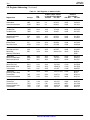
Chapter 2
Table 2-1.
Table 2-2.
USC Registers, in Address Order ........................................................ 2-12
USC Registers, in Alphabetical Order .................................................. 2-13
© 1997 by Zilog, Inc. All rights reserved. No part of this document
may be copied or reproduced in any form or by any means
without the prior written consent of Zilog, Inc. The information in
this document is subject to change without notice. Devices sold
by Zilog, Inc. are covered by warranty and patent indemnification
provisions appearing in Zilog, Inc. Terms and Conditions of Sale
only. Zilog, Inc. makes no warranty, express, statutory, implied or
by description, regarding the information set forth herein or
regarding the freedom of the described devices from intellectual
property infringement. Zilog, Inc. makes no warranty of merchantability or fitness for any purpose. Zilog, Inc. shall not be
responsible for any errors that may appear in this document.
Zilog, Inc. makes no commitment to update or keep current the
information contained in this document.
UM97USC0100
Zilog’s products are not authorized for use as critical components in life support devices or systems unless a specific written
agreement pertaining to such intended use is executed between
the customer and Zilog prior to use. Life support devices or
systems are those which are intended for surgical implantation
into the body, or which sustains life whose failure to perform,
when properly used in accordance with instructions for use
provided in the labeling, can be reasonably expected to result in
significant injury to the user.
Zilog, Inc. 210 East Hacienda Ave.
Campbell, CA 95008-6600
Telephone (408) 370-8000
Telex 910-338-7621
FAX 408 370-8056
Internet: http://www.zilog.com
ix
UM009402-0201
Z16C30 USC®
USER'S MANUAL
ZILOG
USER’s MANUAL
CHAPTER 1
INTRODUCTION
1.1 INTRODUCTION
The Universal Serial Controller (USC®) is the next-generation successor to Zilog’s popular SCC family of multiprotocol serial controllers, and is recommended for new
designs. Compared to the SCC family and most competing devices, the USC features more serial protocols, a 16or 8-bit data bus, higher data rates, larger FIFOs, better
support for DMA operation, and more convenient software
handling. The USC can handle higher data rates because
it takes its timing reference from the software-selected
receive and transmit clocks and the host bus control
signals, rather than from a separate “bus clock” or “master
clock”.
1.2 FEATURES
■
Two Full-Duplex Multi-Protocol Serial Controllers
■
Supports External DMA Channels with two Request
and two Acknowledge Lines
■
Serial Data Rates to 10 Mbits/Second
■
32-Character Transmit and Receive FIFOs for each
Channel
■
8- or 16-Bit Transfers for both Serial Data and
Registers
■
Flexible Adaptation to Various System Buses
■
Serial Modes Include Asynchronous, Bisync, SDLC,
HDLC, Ethernet, and Nine-Bit
■
Two Baud Rate Generators per Channel
■
■
Async Features Include False-Start Filtering, Stop Bit
Length Programmable by 1/16-bit steps, Parity
Generation/Checking, Break Generation/Detection
■
HDLC/SDLC Features Include 8-Bit Address Checking,
Extended Address Support, 16/32 bit CRC,
Programmable Idle State, Auto Preamble Option, Loop
Mode
■
Sync Features Include 2 to 16-Bit Sync Pattern, Sync
Strip Option, 16/32-bit CRC, Programmable Idle State,
Auto Preamble Option, X.21 XMIT/RCV Slaving
■
Improved Bus/Serial Interlocks Prevent extra Rx DMA
Characters and Ensure Correct FIFO Fill Level
Reporting
■
Flexible Interrupt Modes Including Interrupt
Acknowledge Daisy Chain
Digital Phase Locked Loop for each Channel
■
High-Speed, Low Power CMOS Technology
■
Carrier Detect, Clear to Send, and Two Serial Clock
pins for each Channel
■
68-Pin PLCC
■
Transmit and Receive Frame-Length Counters for
each Channel
UM97USC0100
UM009402-0201
1-1
Z16C30 USC®
USER'S MANUAL
ZILOG
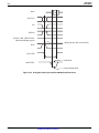
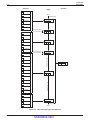
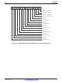
1.3 LOGIC SYMBOL
VDD
/RESET
/CS
A//B
D//C
/AS
R//W
/DS
/RD
/WR
/SITACK
/PITACK
IEIA, B
/RxACKA,B
/TxACKA,B
/RxCA,B
/TxCA,B
RxDA,B
/CTSA,B
/DCDA,B
AD15-AD0
/WAIT//RDY
Z16C30
USC
/INTA,B
IEOA,B
/RxREQA,B
/TxREQA,B
/TxDA,B
VSS
Figure 1-1. USC Logic Symbol
1-2
UM009402-0201
UM97USC0100
Z16C30 USC®
USER'S MANUAL
ZILOG
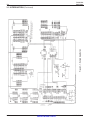
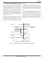
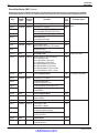
VDD
VDD
VDD
3
2
1
68 67 66 65 64 63 62 61
/TxACKB
/RESET
4
/PITACK
/CS
5
R//W
D//C
6
/W/R
A//B
7
/RD
/SITACK
8
/DS
/WAIT//RDY
9
/AS
/TxACKA
1.4 PACKAGING
/RxACKA
10
60
/RxACKB
/INTA
11
59
/INTB
IEIA
12
58
IEIB
IEOA
13
57
/IEOB
VSS
14
56
VSS
VDD
15
55
VDD
AD0
16
54
AD8
AD1
17
53
AD9
AD2
18
52
AD10
AD3
19
51
AD11
AD4
20
50
AD12
AD5
21
49
AD13
AD6
22
48
AD14
AD7
23
47
AD15
VSS
24
46
VSS
VDD
25
45
VDD
/RxREQA
26
44
/RxREQB
Z16C30 USC
(Top View)
/TxREQB
/RxCB
RxDB
/DCDB
/TxCB
TxDB
/CTSB
VSS
VSS
VSS
/CTSA
TxDA
/TxCA
/DCDA
RxDA
/RxCA
/TxREQA
27 28 29 30 31 32 33 34 35 36 37 38 39 40 41 42 43
Figure 1-2. USC® 68-Pin PLCC Pinout
UM97USC0100
UM009402-0201
1-3
Z16C30 USC®
USER'S MANUAL
ZILOG
1.5 OVERVIEW OF THE USC AND THIS MANUAL
The following descriptions and Tables should be helpful in
initial evaluation of the USC® and in finding your way
around this document. Subjects in the Tables are arranged
in the same order they are covered in Chapters 2 and 4-8.
tions. This Chapter focuses on software aspects of using
the USC while Chapter 4 is more hardware-oriented.
Tables 1-3 and 1-4 show the major subjects that you can
find in Chapter 5.
1.5.1 Bus Interfacing
1.5.4 DMA Operation
Chapter 2 describes interfacing the USC to a processor or
backplane bus. The USC includes several flexible interfacing options as described in Table 1-1. Some of these
options are controlled by the Bus Configuration Register
(BCR), which is implicitly the destination of the first write to
the USC after a Reset, and is then no longer accessible to
software.
Chapter 6 describes how to use the USC with DMA
channels, and is outlined in Table 1-5.
1.5.2 Serial Interfacing
Chapter 4 covers Serial Interfacing, the “other side” of
hardware design from Bus Interfacing. Table 1-2 summarizes the Serial Interfacing features of the USC, which
include Clock Selection, Baud Rate Generation, serial
data Encoding and Decoding, a Digital Phase Locked
Loop for reconstructing clocking from received data, and
“modem control” pins.
1.5.3 Serial Modes and Protocols
1.5.5 Interrupts
While Chapters 4-6 mention which conditions and events
can be enabled/armed to interrupt the processor, Chapter
7 pulls together all aspects of the USC’s extensive interrupt
capabilities, including interrupt acknowledge cycles, vectors, and use of Interrupt Under Service bits to implement
nested interrupts. Table 1-6 summarizes the subject.
1.5.6 Software Summary
Chapter 8 contains only a small amount of new material: a
few software-related matters that didn’t seem to fit in
anywhere else. The bulk of the Chapter is the Register
Reference tables that summarize the use and function of
each bit and field in each register in the USC.
Chapter 5 covers how to program the Transmitter and
Receiver to handle many different protocols and applica-
1-4
UM009402-0201
UM97USC0100
Z16C30 USC®
USER'S MANUAL
ZILOG
Table 1-1 Bus Interfacing Features of the USC (Chapter 2)
Multiplexed or Separate Address and Data Bus(es)
can be selected for processor access to USC registers.
Read/Write Control Signals
Separate Read and Write strobes, or Data strobe and Direction
control can be used. Only one set of signals should be
connected to the host processor; the other should be pulled
up.
8- or 16-Bit Data Bus
DMA efficiency and bandwidth are doubled by using a 16-bit
bus, and software size and tediousness is improved as well.
With an 8-bit data bus and non-multiplexed Address and Data,
the bus pins that would otherwise be unused can be used for
register addressing from the processor.
Ready, Wait, or Acknowledge Handshaking
can be selected for processor cycles. If Wait signalling is
selected, the USC drives Wait for interrupt acknowledge cycles
but not for register accesses — its 60 nanosecond register
access time is fast enough for no-Wait operation in almost all
applications. If Acknowledge signaling is selected, the part
drives the Acknowledge line for both interrupt acknowledge
cycles and register accesses.
Interrupt Acknowledge Cycles
Separate inputs are provided for “Status line” vs. “pulse”
signalling. In the latter case single-pulse or double-pulse
cycles can be selected. The USC can also be used on buses
that don’t include Interrupt Acknowledge cycles.
Direct or Indirect Register Addressing
The board designer can conserve the address space occupied by the USC by requiring software to write register addresses into the USC, or can maximize software efficiency by
presenting register addresses directly. On a non-multiplexed
16-bit data bus, the latter choice requires external components/logic to multiplex the low-order bits of the address onto
the AD pins.
Registers
There are 32 16-bit registers in each channel of the USC,
including three selectable subregisters in the MSbyte of two of
them.
Big- or Little-Ending Byte Ordering
Motorola or Intel style addressing can be selected for serial
data. Byte addressing within the USC’s 16-bit registers is
inherently Little-Endian/Intel style.
UM97USC0100
UM009402-0201
1-5
Z16C30 USC®
USER'S MANUAL
ZILOG
1.5.6 Software Summary (Continued)
Table 1-2. Serial Interfacing Features of the USC (Chapter 4)
Clock Selection
Clocking for the Transmitter and Receiver can come from the
/RxC or /TxC pins, and can be used directly or can be divided by 4, 8,
16, or 32 by Counters 0 and 1, and/or by any value from 1 to 65,536 by
Baud Rate Generators 0 and 1. Or, clocking can come from the Digital
Phase Locked Loop (DPLL) module, which tracks transitions on the
RxD pin.
Clock Output
Clocking can also be driven out on the /TxC or /RxC pin for use by onboard logic, a modem or other interface.
CTR0, CTR1
These two 5-bit free-running counters can each divide /RxC or /TxC by
4, 8, 16, or 32. They can provide the Transmit or Receive bit clocks
directly, or can act as “prescalers” for the Baud Rate Generators.
Baud Rate Generators
BRG0 and BRG1 are 16-bit counters, each of which can divide /RxC,
/TxC, or the output of CTR0 or CTR1 by any value from 1 to 65,536. They
can source the Transmit or Receive bit clocks, act as the reference
clock for the DPLL, or can be used as timers on either a polled or
interrupt-driven basis. They can be stopped and started by software,
and can run continuously or stop when they reach zero. Their period
(time constant) values can be reprogrammed dynamically, effective
immediately or when the BRG counts down to zero.
Digital-Phase Locked Loop
The DPLL can divide /RxC, /TxC, or the output of BRG0 or BRG1 by 8,
16, or 32, while resynchronizing to transitions on RxD, to recover a
Receive clock from the Receive data signal. This can be done only
when the received data stream includes enough transitions to keep the
recovered clock synchronized to the data. NRZI-Space encoding of
HDLC/SDLC frames, or Biphase (FM) encoding with any protocol,
guarantees such data transitions.
Data Encoding
The USC can encode transmitted data and decode received data in
NRZI-Mark, NRZI-Space, Biphase-Mark (FM1), Biphase-Space (FM0),
Biphase-Level (Manchester), or Differential-Biphase-Level modes.
These encodings are used in various applications to maintain synchronization between transmitting and receiving equipment.
Echoing and Looping
Received data can be repeated onto TxD, or transmit data can be
looped back to the Receiver for testing.
Modem Controls and Interrupts
Carrier Detect and Clear to Send inputs can auto-enable the
Receiver and Transmitter, respectively. Rising and/or falling edges on
these pins can cause interrupts, as can edges on the Transmit and
Receive Clock pins (if they’re not used for clocking), and/or the
Transmit and Receive Request pins if they’re not used for DMA
requests.
DMA Controller Interface
Each channel of the USC provides Tx and Rx Request outputs for
connection to a DMA controller, and Tx and Rx Acknowledge inputs for
“flyby” (single-cycle) DMA operation. The Acknowledge pins can be
used for other purposes if “flowthrough” (two-cycle) DMA controller is
employed. Both Request and Acknowledge pins can be used for other
purposes if no DMA controller is used.
1-6
UM009402-0201
UM97USC0100
Z16C30 USC®
USER'S MANUAL
ZILOG
Table 1-3. Serial Controller Features of the USC
Major Protocol Categories
Chapter 4 begins with a small tutorial on the differences between Asynchronous,
Character-Oriented Synchronous, and Bit-Oriented Synchronous (Packet)
protocols.
Asynchronous Protocols
In addition to classic Async, the USC can handle the following variations:
■ Isochronous (1X rather than 16-64X clock)
■ Nine-Bit (Address Wake-up — an extra bit signifies Address/Data)
Character-Oriented
Synchronous Protocols
Bit-Oriented Synchronous
Protocols
■
■
■
■
■
■
External Sync (Receive only: simple character assembly)
Monosync (1-character sync pattern, no hardware framing)
Bisync (2-character sync pattern, no hardware framing)
Transparent Bisync (Bisync + hardware support for Transparency)
Slaved Monosync (Xmit only; X.21 Tx character alignment to Rx)
IEEE 802.3 (Ethernet; requires external collision detect and backoff)
■
■
HDLC/SDLC
HDLC/SDLC Loop (RxD is repeated on TxD except when Xmit is
enabled and triggered by a received Go Ahead/Abort sequence)
Character Length
is programmable from 1 bit/character to:
■ 8 bits including Parity, if any, in synchronous modes
■ 8 bits plus Parity, if any, in Async mode
■ 8 bits plus Parity plus the Address/Data bit in Nine-Bit mode
CRC Generation/Checking
In synchronous modes, the USC will generate and check CRC-CCITT, CRC-16, or
CRC-32 codes for each frame or message. For character-oriented modes other
than 802.3, software can selectively control which characters are included in the
CRC, for both transmitting and reception. For HDLC/SDLC and 802.3, CRC status
can be stored in memory for each received frame.
Parity Checking
Asynchronous or Synchronous modes. Odd/Even/Mark/Space/None.
Transmit Status Reporting
Optional interrupt on: Preamble Sent, Idle Sent, Abort Sent, End of Frame/
Message, CRC Sent, Underrun No interrupt: All Sent, Tx Empty
Receive Status Reporting
Optional Interrupt on: Exited Hunt, Idle Received, Break, Abort (immediate or
synchronized with the RxFIFO), Rx Boundary (end of frame/message), Parity
Error, Overrun. No interrupt: Short Frame, Code Violation Type, CRC Error,
Framing Error, Rx Character Available
Character Counters
These 16-bit counters decrement for each character received or fetched from
memory for transmission. The Tx CC can control the length of Tx frames in
synchronous modes using DMA. The Rx CC tracks the length of each Rx frame
in synchronous modes using DMA, and optionally interrupts in case an Rx frame
is too long.
RCC FIFO
A four-deep store for ending Rx Character Counter values for each frame.
UM97USC0100
UM009402-0201
1-7
Z16C30 USC®
USER'S MANUAL
ZILOG
Table 1-4. More Serial Controller Features of the USC
Transmit Control Blocks
A Transmit DMA channel can fetch the Tx CC frame length and other control info
for each frame/message, before the frame in the memory buffer.
Receive Status Blocks
The Rx DMA channel can provide the frame status (including CRC status) for
each frame/message after the frame. Optionally it can also provide the the Rx
CC frame length residual, although this is only useful in Rx DMA applications in
which software can read the number of bytes/words that were stored, from the
DMA channel.
Commands
Software can write various command codes to 3 different register fields in each
channel, to control the operation of the channel. Commands can be divided into
those that select a long-term configuration of a channel (like selecting which
serial character in a 16-bit word comes first), those that make the part perform
a time-sequenced action (like sending an Abort sequence), and those that
change the state of the part immediately (like purging a FIFO).
Software Reset
Software can reset a USC channel by writing a central register bit, similarly to
a hardware-signaled Reset.
Rx and Tx FIFO Storage
32-character FIFOs stand between the Transmit Data Register and the Transmitter, and between the Receiver and the Rx Data Register. Fill level counters
track how many characters are in each FIFO, and independently programmable threshold values determine when DMA operation will be triggered to fill
or empty them, and/or when an interrupt will be requested.
Between Frames/Messages
In synchronous modes the Transmitter will do the following before the first
data character of each frame or message, and/or after the last one:
■ optionally send a 8-to 64-bit Preamble for PLL synchronization or minimum inter-frame timing
■ send an "opening" sync sequence or Flag
■ After the last character from memory, sending the CRC accumulated by the
USC is optional. Thus, a CRC received with a frame can be sent back out
without being regenerated.
■ send a "closing" Flag or Sync
■ send a selected "idle" pattern unless/until the next frame is ready to be sent
Waiting for Software Response
Software can select 3 optional interlocks between frames, to allow it to do
real-time processing on a frame-by-frame basis.
1-8
UM009402-0201
UM97USC0100
Z16C30 USC®
USER'S MANUAL
ZILOG
Table 1-5. DMA Features of the USC
Flowthrough or Flyby
The USC can be used with DMA controllers in a “flowthrough” mode,
in which the REQ line from the USC tells the DMAC when to transfer data
by means of separate accesses to the USC and to memory. Alternatively, the USC and DMA can operate in a “flyby” mode, in which there’s
also an ACK line from the DMAC to tell the USC when to drive data to
the memory or when to capture data from the memory. Flyby operation
requires only one bus cycle per (pair of) character(s).
DMA Requests
A USC can provide separate Transmit and Receive DMA Request
outputs from each of its two channels, that become active when the
relevant FIFO reaches a software-selected level of emptiness or
fullness, and stay active until the FIFO is filled or emptied. The Receive
Request for a channel operating in a synchronous block oriented mode
(e.g., HDLC) will also go active when the end of a message or frame is
received.
Separating Receive Frames
Chapter 5 ends with a description of how the “Wait for Rx Trigger”
feature can be used to separate received frames into individual
memory buffers, by withholding the Rx DMA Request for the data in a
new frame until after software has read out the length of the frame and/
or programmed the DMA channel with the buffer address for the new
frame.
UM97USC0100
UM009402-0201
1-9
Z16C30 USC®
USER'S MANUAL
ZILOG
Table 1-6. Interrupt Features of the USC
Interrupt Acknowledge
Daisy Chaining
was one of Zilog’s original contributions to microprocessor architecture. On the USC
its use (to determine which of several interrupting devices to service first) is optional,
and performance is much improved compared to older devices.
External Interrupt Control
can be used instead of a daisy chain to implement interrupt priority schemes other
than strict priority, such as “fairness”, rotating, or first-come first-served.
Types
of interrupts that can be selectively enabled or disabled include Receive Status,
Receive Data, Transmit Status, Transmit Data, I/O Pin, and Miscellaneous.
Receive Status Interrupt
sources that can be selectively armed or disarmed include Exited Hunt, Idle
Received, Break, Abort (immediate and/or synchronized to received data), End of
Frame/Message, Parity Error, and RxFIFO Overrun.
Receive Data Interrupt
can occur when the RxFIFO reaches a programmed level of fullness.
Transmit Status Interrupt
sources that can be selectively armed or disarmed include Preamble Sent, Idle
Sent, Abort Sent, End of Frame/Message Sent, CRC Sent, and Tx Underrun.
Transmit Data Interrupt
can occur when the TxFIFO reaches a programmed level of emptiness.
I/O Pin Interrupt
sources that can be selectively armed or disarmed include rising and/or falling
edges on the /DCD, /CTS, /RxREQ, /TxREQ, /RxC, and /TxC pins.
Miscellaneous Interrupt
sources that can be selectively armed or disarmed include Rx Character Counter
Underflow, DPLL Sync Loss, Baud Rate Generator 0 zero, and BRG1=0.
Nested Interrupts
are fully supported in that the USC includes an Interrupt Pending and Interrupt
Under Service bit for each type of interrupt.
Interrupt Acknowledge Cycles
The USC is compatible with a wide variety of processors in that the signal that
identifies an acknowledge cycle can be sampled like an address bit, or can carry
a single or double pulse similar to a read or write strobe.
Interrupt Vectors
The USC can include identification of the highest priority requesting type of interrupt
in the vector that it returns during an interrupt acknowledge cycle.
Non-Acknowledging Buses
Software can simulate the effects of interrupt acknowledge cycles if the USC is used
on a bus that doesn’t provide such cycles, like the ISA (AT) bus.
1-10
UM009402-0201
UM97USC0100
Z16C30 USC®
USER'S MANUAL
ZILOG
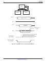
Transmitter
DPLL
Counters
BRG0, BRG1
Receiver
Serial Clock
Logic
Transmit
FIFO
Receive
FIFO
Interrupt
Control
Channel A
16-Bit Internal
Bus
Interface
Host
Processor
Data Bus
Channel B
Interrupt
Control
DMA
Controller,
System
Memory
Transmit
FIFO
Receive
FIFO
Serial Clock
Logic
Transmitter
DPLL
Counters
BRG0, BRG1
Receiver
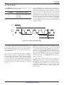
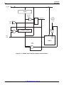
Figure 1-3. USC® Block Diagram
UM97USC0100
UM009402-0201
1-11
Z16C30 USC®
USER'S MANUAL
ZILOG
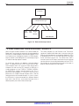
1.6 DEVICE STRUCTURE
Figure 1-1 shows the basic structure of the USC. The Bus
Interface module stands between the external bus pins
and an on-chip 16-bit data bus that interconnects the other
functional modules. It includes several flexible bus interfacing options that are controlled by the Bus Configuration
Register (BCR). The BCR is automatically the destination
of the first write cycle from the host processor to the USC
after a Reset. After that it is no longer accessible to the host
software.
have to detect and synchronize start bits, check parity and
stop bits, calculate and check CRCs, detect flag, abort
and idle sequences, recognize control characters including transparency considerations, decode the serial data
and clock extraction using any of several encoding
schemes, and/or enable and disable reception based on
the DCD input pin. The Receivers’ checking functions
generate several status bits associated with each character, that accompany the characters through the Receive
FIFOs.
1.6.1 The Transmit Data Path
Either the host processor or an external DMA channel can
write transmit data into a channel’s Transmit First-In, FirstOut (FIFO) memory. At any time, a Transmit FIFO can be
empty or can contain from 1 to 32 characters to be
transmitted. Characters written into the TxFIFO become
available to the Transmitter in the order in which they were
written.
While the host processor can itself write data into the
Transmit FIFOs, it’s more efficient to use external Transmit
DMA channels to fetch the data. The host can program a
USC channel so that its Transmitter will trigger its DMA
controller to fill its FIFO at varying degrees of FIFO “emptiness”. Selecting this point involves balancing the probability and consequences of “underrunning” the transmitter, against the overhead for the DMA channel to acquire
control of the host bus more often.
The serial Transmitters take characters from the Transmit
FIFOs and convert them to serial data on the TxD pins.
While this function is conceptually simple, the USC supports many complex serial protocols, which increases the
complexity of the Transmitters dramatically. Depending on
the serial mode selected, the Transmitters may do any of
the following in addition to parallel-serial conversion: start,
stop, and parity bit generation, calculating and sending
CRCs, automatic generation of opening and closing flags,
encoding the serial data into any of several formats that
guarantee transitions and carry clocking with the data,
and/or controlling transmission based on the CTS pin.
1.6.2 The Receive Data Path
In general, the functions of the Receivers are the inverse of
those of the Transmitters: they monitor the serial data on
the RxD pin, organize it according to the serial mode
selected by the software, and convert the data to parallel
characters that they place in the Receive FIFOs. Again,
there is more to the process than just serial-parallel conversion. Depending on the serial mode the Receivers may
1-12
The Receive FIFOs can hold up to 32 characters and their
associated status bits. As the receivers write entries into
their FIFOs, the entries become available to either the host
processor or external Receive DMA channels. As on the
transmit side, the Receive FIFOs include detection logic
for various degrees of “fullness”. Separate thresholds
control the point at which a channel starts requesting its
DMA channel starts to refill its FIFO, and at which a channel
requests an interrupt. Besides the main Receive FIFOs,
each channel has a 4-entry RCC FIFO that can hold values
indicating the length of up to four received frames.
While the host processor can access data from the Receive FIFOs, it’s more efficient to use external Receive
DMA channels to transfer the data directly into buffer areas
in memory. The USC can provide the status (and optionally
the RCC value at the end) of each frame in the serial data
stream, after the last character of the frame.
1.6.3 Clocking
Each channel includes a Serial Clocking Logic section that
creates the clocking signals for the channel’s Transmitter
and Receiver. Software can program the clocking logic to
do this in various ways based on one or two external
clock(s) for each channel. Each channel also includes a
Digital Phase Locked Loop (DPLL) circuit that can recover
clocking from encoded data on RxD.
1.6.4 Interrupts
There’s also an Interrupt Control section in each channel,
that gathers the various “request” lines from the Transmitter and Receiver, and takes care of requesting host interrupts and responding to host interrupt-acknowledge cycles
or to software equivalents. Interrupt operation depends on
the data written to the Bus Configuration Register and on
several registers in the Receiver and Transmitter. There
are a separate set of interrupt pins for each channel so that
external logic can control their relative priority.
UM009402-0201
UM97USC0100
Z16C30 USC®
USER'S MANUAL
ZILOG
1.7 DOCUMENT STRUCTURE
The Chapters in this manual attempt to provide the firsttime reader with a staged and gradual introduction to the
USC. The manual is structured according to the USC’s
major internal blocks and various aspects of their operation, rather than as a list and description of each of its
registers. The various registers and fields are covered in
conjunction with the facilities that they report on and
control. Chapter 8 then reviews the general programming
model and includes a concise description of each register
bit and field for quick reference.
The actual timing parameters and electrical specifications
of the IUSC are given in the companion publication 'USC
Product Specification'.
© 1997 by Zilog, Inc. All rights reserved. No part of this document
may be copied or reproduced in any form or by any means
without the prior written consent of Zilog, Inc. The information in
this document is subject to change without notice. Devices sold
by Zilog, Inc. are covered by warranty and patent indemnification
provisions appearing in Zilog, Inc. Terms and Conditions of Sale
only. Zilog, Inc. makes no warranty, express, statutory, implied or
by description, regarding the information set forth herein or
regarding the freedom of the described devices from intellectual
property infringement. Zilog, Inc. makes no warranty of merchantability or fitness for any purpose. Zilog, Inc. shall not be
responsible for any errors that may appear in this document.
Zilog, Inc. makes no commitment to update or keep current the
information contained in this document.
Zilog’s products are not authorized for use as critical components in life support devices or systems unless a specific written
agreement pertaining to such intended use is executed between
the customer and Zilog prior to use. Life support devices or
systems are those which are intended for surgical implantation
into the body, or which sustains life whose failure to perform,
when properly used in accordance with instructions for use
provided in the labeling, can be reasonably expected to result in
significant injury to the user.
UM97USC0100
We at Zilog hope that this newly structured manual will
make the USC more easily understandable and accessible. Naturally, it’s impossible to write at the right level for
all readers; newcomers will find some parts hard going,
while experts will undoubtedly tire of full explanations of
matters that “everyone knows”. Our target audience is
neither newcomers nor experts, but midway between:
working engineers with some datacom background.
Zilog, Inc. 210 East Hacienda Ave.
Campbell, CA 95008-6600
Telephone (408) 370-8000
Telex 910-338-7621
FAX 408 370-8056
Internet: http://www.zilog.com
UM009402-0201
1-13
Z16C30 USC®
USER'S MANUAL
ZILOG
USER’s MANUAL
CHAPTER 2
BUS INTERFACING
2.1 INTRODUCTION
The USC® can be used in systems with various microprocessor or backplane buses. Its flexibility with respect to
host bus interfacing derives from its Bus Configuration
Register (BCR), from on-chip logic that monitors bus
activity before software writes the BCR, and from certain
other registers in the serial channels. This section describes how to use these facilities to interface the USC to
a variety of host microprocessors and buses.
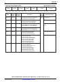
2.2 MULTIPLEXED/NON-MULTIPLEXED OPERATION
One important distinction among buses is whether they
include separate sets of lines for addresses and for data,
or whether the same set of lines carries multiplexed addresses and data. On a multiplexed bus, the USC captures
addressing at rising edges on /AS. If this signaling is the
same as that used on the host bus (as with a Zilog 16C0x),
then the USC’s /AS pin can be directly connected to the
corresponding bus signal. Figure 2-1 shows such a system.
AD15:AD0
/AS
16C01
AD15:AD0
/AS
USC
Figure 2-1. Simple Multiplexed System
UM97USC0100
UM009402-0201
2-1
Z16C30 USC®
USER'S MANUAL
ZILOG
2.2 MULTIPLEXED/NON-MULTIPLEXED OPERATION (Continued)
An 80x86-based system differs only in that the processor’s
ALE signal has to be inverted to produce /AS for the USC.
A15-A0
D15-D0
Cntrl Signals
Figures 2-2 and 2-3 illustrate two ways to interface the USC
to a non-multiplexed host bus. Figure 2-2 includes minimum hardware but requires that software write the register
address into the USC each time it is going to access a
register. In this mode the USC’s /AS pin should be pulled
up to ensure a constant high logic level. Figure 2-3 includes drivers to sequence the low-order bits of the host
address onto the USC’s AD lines, and logic to synthesize
a pulse on the /AS pin. This interfacing method has the
advantage that software can directly address the USC’s
registers.
The USC monitors the /AS pin from the time the /RESET pin
goes high until the software writes the Bus Configuration
Register. If it sees /AS go low at any point in this period,
then after the software writes the BCR, the USC captures
the state of the low-order AD lines, A//B, C//D, and /CS, at
each rising edge of /AS. If /AS remains high, software may
have to write each register address into the Channel
Command/ Address Register (CCAR) before reading or
writing a register. (If the host bus only includes 8 data lines,
AD13-AD8 can carry register addresses.)
Control
Logic
/AS
USC
/RD, /WR
AD15-AD0
Figure 2-3. User-Friendly Interface to
Non-Multiplexed Bus
D15:D0
/AS
68000
AD15:AD0
VCC
/AS
USC
Figure 2-2. Simple Interface to Non-Multiplexed Bus
2-2
UM009402-0201
UM97USC0100
Z16C30 USC®
USER'S MANUAL
ZILOG
2.3 READ/WRITE DATA STROBES
Another difference among host buses is the way in which
read and write cycles are signalled and differentiated.
Figures 2-4 and 2-5 show two standard methods supported by the USC. In Figure 2-4, the bus includes separate strobe lines for read and write cycles, commonly
called /RD and /WR. In Figure 2-5, the bus includes a data
strobe line, /DS, that goes low for both read and write
cycles, and a R//W line that differentiates read cycles from
writes. The USC includes pins for all four of these signals.
The two that match up with host bus signals should be
connected to those signals. The two unused pins should
be pulled up to a high level.
Read Operation:
R//W
DS*
Data Bus
Write Operation:
R//W
Read Operation:
RD*
DS*
WR*
Data Bus (Slave)
Data Bus
Figure 2-5. R//W and /DS Signaling
Write Operation:
There is no programmable option for the distinction between /RD-/WR and R//W-/DS operation. The USC simply
responds to either pair of lines, which is why it’s important
to pull up the unused pair. Also, the USC doesn’t demand
that the R//W line remain valid throughout the assertion of
/DS. It captures the state of R//W at the leading/falling edge
of /DS, so that R//W need only satisfy setup and hold times
with respect to this edge.
RD*
WR*
Data Bus
Figure 2-4. /RD and /WR Signaling
UM97USC0100
Only one among the bus signals /DS, /RD, /WR, and
/PITACK may be active at a time. This prohibition also
includes /RxACKA, /RxACKB, /TxACKA, and /TxACKB
when these pins are used as DMA acknowledge signals.
(Chapter 5 covers DMA interfacing including the “ACK”
signals, and Chapter 6 describes the USC’s interrupt
features including /PITACK). If the USC detects more than
one of these inputs active simultaneously, it enters an
inactive state from which the only escape is via the /RESET
pin.
UM009402-0201
2-3
Z16C30 USC®
USER'S MANUAL
ZILOG
2.4 BUS WIDTH
Another major difference among host buses is the number
of data bits that can be transferred in one cycle. Software
can configure the USC to transfer 16 bits at a time, in which
case it is still possible to transfer 8 bits when this is
necessary or desirable. Or, software can restrict operation
to transferring only 8 bits at a time, on the AD7-AD0 pins.
This leaves the AD15-AD8 pins unused: another BCR
option allows them to carry register addresses. The latter
option allows software to directly address USC registers
even on a non-multiplexed bus, without having to write an
address into the USC before it accesses a register.
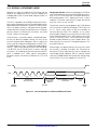
2.5 ACK VS. WAIT HANDSHAKING
The final major difference among host buses involves the
nature of the handshaking signals that slave devices use
for speed-matching with masters. Figure 2-6 illustrates the
three variations in common use. In the first, which we’ll call
Wait signaling, if a master selects a slave and the slave
cannot capture write data or provide read data within the
time allowed to keep the master operating at full speed, it
quickly (combinatorially) drives a Wait output low, and then
returns it to high when it’s ready to complete the cycle.
Some peripheral devices have Wait outputs that are opencollector or open-drain, which can be tied together for a
negative logic wired-Or function. Because the USC drives
its /WAIT//RDY output high or low on a full-time basis, a
logic gate must be used to negative-logic OR (positivelogic AND) its /WAIT//RDY output with the /WAIT signal(s)
for other slaves, to produce the /WAIT input to the master
(e.g., to the processor).
In the second scheme, “Acknowledge” signaling, all slaves
must respond when the master directs a cycle to them, by
driving an Acknowledge signal (sometimes called /DTACK)
low to allow the master to complete the transfer, and
keeping it low until the master does so. As with the previous
scheme, some peripherals provide slave Ack outputs that
are open-collector or open-drain, which can be tied together for a negative logic wired-Or function. Because the
USC drives its /WAIT//RDY output high or low on a full-time
basis, a logic gate must be used to negative-logic OR its
/WAIT//RDY output with the /ACK signals for other slaves,
to produce the Acknowledge input to the master.
2-4
In the third scheme, “Ready” signaling, all slaves must
respond when the master directs a cycle to them, by
driving a Ready signal high to allow the master to complete
the transfer, and keeping it high until the master does so.
This scheme differ from Wait signaling in the default state
of the handshaking signal between cycles (high for Wait
signaling, low for Ready). It has similar timing as Ack
signaling, but differs in the polarity of the handshaking
signal. With Ready signaling, the board designer must
include a logic gate to positive-logic OR the various slaves’
Ready lines to produce a composite Ready input for the
bus master(s).
The USC supports Acknowledge and Ready signaling for
all cycles, and Wait signaling for interrupt acknowledge
cycles. The USC register access times should be short
enough to avoid the need for Wait signaling on all but the
fastest processors. The board designer can combine the
USC’s /WAIT//RDY output with similar signals from other
slaves, by means of an external logic gate or (for Acknowledge and Wait) an external tri-state or open-collector
driver.
If software writes the Bus Configuration Register (BCR) at
an address that makes the A//B pin low, the USC drives
/WAIT//RDY low as an “Acknowledge” signal, while if
software writes the BCR with A//B high, the USC drives
/WAIT//RDY as a “wait” signal.
UM009402-0201
UM97USC0100
Z16C30 USC®
USER'S MANUAL
ZILOG
RD* or WR*
or DS*
WAIT*
ACK*
Ready
Figure 2-6. A Fast and Slow Cycle, with Three Kinds of Handshaking
2.6 PIN DESCRIPTIONS
/RESET. Reset (input, active low). A low on this line places
the USC in a known, inactive state, and conditions it so that
the data, from the next write operation that asserts the /CS
pin, goes into the Bus Configuration Register (BCR) regardless of register addressing. /RESET should be driven
low as soon as possible during power-up, and as needed
when restarting the overall system or the communications
subsystem.
AD15-AD0. Address/Data Bus (inputs/tri-state outputs).
These lines carry data between the controlling microprocessor and the USC, and may also carry multiplexed
addresses of registers within the USC. If the USC is used
with an external DMA controller, these lines also carry data
between the USC and system memory or the DMA controller. AD15-AD0 can be used in a variety of ways based on
whether the USC senses activity on /AS after Reset, and on
the data written to the Bus Configuration Register (BCR).
/CS. Chip Select (input, active low). A low on this line
indicates that the controlling microprocessor’s current bus
cycle refers to a register in the USC. The USC ignores /CS
when a low on /SITACK or /PITACK indicates that the
current bus operation is an interrupt acknowledge cycle.
On a multiplexed bus the USC latches the state of this pin
at rising edges on /AS, while on a non-multiplexed bus it
latches /CS at leading/falling edges on /DS, /RD, or /WR.
A//B. Channel Select (input, high indicates “channel A”).
Cycles with /CS low, and /SITACK, /PITACK, and this pin
both high, access registers for channel A. Cycles with
/SITACK and /PITACK high, and /CS and this pin both low,
access registers for channel B. The state of this line when
the Bus Configuration Register is written determines “wait
UM97USC0100
vs. acknowledge” operation, as described later in this
chapter. On a multiplexed bus the USC latches the state
of this pin at rising edges on /AS, while on a non-multiplexed bus it latches the state at leading/falling edges on
/DS, /RD, or /WR.
D//C. Data/Control (input, high indicates Data). A read
cycle with /CS low, and /SITACK, /PITACK, and this pin
high, fetches data from the receive FIFO of the channel
selected by A//B, via its Receive Data Register (RDR). A
write cycle with the same conditions writes data into that
channel’s transmit FIFO via its Transmit Data Register
(TDR). Cycles with /SITACK and /PITACK high and both
/CS and this pin low read or write a USC register. On a
multiplexed bus the USC determines which register to
access from the low-order AD lines at the rising edge of
/AS. On a non-multiplexed bus it typically selects the
register based on the LSBits of the serial controller’s
Channel Command/Address Register. On a multiplexed
bus the USC latches the state of this pin at rising edges on
/AS, while on a non-multiplexed bus it latches the state at
leading/falling edges on /DS, /RD, or /WR.
/AS. Address Strobe (input, active low). After a reset, the
USC’s bus interface logic monitors this signal to see if the
host bus multiplexes address and data on AD15-AD0. If
the logic sees activity on /AS before (or as) software writes
the Bus Configuration Register, then in subsequent cycles
directed to the USC, it captures register selection from the
AD lines, A//B, and D//C on rising edges of /AS.
For a non-multiplexed bus this pin should be pulled up to
+5V. If a processor uses a non-multiplexed bus, yet has an
output called Address Strobe (e.g., 680x0 devices), this
pin should not be tied to the output.
UM009402-0201
2-5
Z16C30 USC®
USER'S MANUAL
ZILOG
2.6 PIN DESCRIPTIONS (Continued)
R//W. Read/Write control (input, low signifies “write”).
R//W and /DS indicate read and write cycles on the bus, for
host processors/buses having this kind of signaling. The
USC samples R//W at each leading/falling edge on /DS.
/DS. Data Strobe (input, active low). R//W and /DS indicate
read and write cycles on the bus, for host processors/
buses having this kind of signaling. It is qualified by /CS low
or /SITACK low. The USC samples R//W at each leading/
falling edge on this line. For write cycles, the USC captures
data at the rising (trailing) edge on this line. In read cycles
the USC provides valid data on the AD lines within the
specified access time after this line goes low, and this data
remains valid until after the master drives this line back to
high.
/RD. Read Strobe (input, active low). This line indicates a
read cycle on the bus, for host processors/buses having
this kind of signaling. It is qualified by /CS low or /SITACK
low. In Read cycles the USC provides valid data on the AD
lines within the specified access time after this line goes
low, and this data remains valid until after the master drives
this line back to high.
/WR. Write Strobe (input, active low). This line indicates
write cycles on the bus, for host processors/buses having
this kind of signaling. It is qualified by /CS low. The USC
captures write data at the rising (trailing) edge of this line.
Only one of /DS, /RD, /WR, or /PITACK may be driven
low in each bus cycle. This restriction also includes
/TxACK and/or /RxACK if they’re used as “flyby” DMA
Acknowledge signals.
/WAIT//RDY. Wait, Ready, or Acknowledge handshaking
(output, active low). This line can carry “wait” or “acknowledge” signaling depending on the state of the A//B input
during the initial BCR write. If A//B is high when the BCR is
written, this line operates thereafter as a Ready/Wait line
for Zilog and some Intel processors. In this mode the USC
asserts this line low until it’s ready to complete an interrupt
acknowledge cycle, but it never asserts this line when the
host accesses one of the USC registers.
If A//B is low when the BCR is written, this line operates
thereafter as an Acknowledge line for Motorola and some
Intel processors. In this mode the USC asserts this line low
for register read and write cycles, and also when it is ready
to complete an interrupt acknowledge cycle.
In any case this is a full time (totem pole) output. The
board designer can combine this signal with similar signals for other slaves, by means of an external logic gate or
a tri-state or open-collector driver.
2-6
/INTA,B. Interrupt Requests (outputs, active low). A channel drives its /INT pin low when (1) its IEI pin is high, (2) one
or more of its interrupt type(s) is (are) enabled and pending, and (3) the Interrupt Under Service flag isn’t set for its
highest priority enabled/pending type, nor for any higherpriority type within the channel. The USC drives these pins
high or low at all times — they are neither tri-state nor opendrain pins.
/SITACK, /PITACK. Interrupt Acknowledge (inputs, active
low). A low on one of these lines indicates that the host
processor is performing an interrupt acknowledge cycle.
In some systems a low on one of these lines may further
indicate that external logic has selected this USC as the
device to be acknowledged, or as a potential device to be
acknowledged. The two signals differ in that /SITACK
should be used for a level-sensitive “status” signal that the
USC should sample at the leading edge of /AS or /DS, while
/PITACK should be used for a single-pulse or double-pulse
protocol. The other, unused pin should be pulled up to a
high level. A channel will respond to an interrupt acknowledge cycle in a variety of ways depending on its /INT and
IEI lines, as described in Chapter 7.
IEIA,B. Interrupt Enable In (inputs, active high). These
signals and the IEO pins can be part of an interruptacknowledge daisy-chain with other devices that may
request interrupts. If a channel’s IEI pin is high outside of
an interrupt acknowledge cycle, and one or more interrupt
type (s) is (are) enabled and pending for that channel, and
the Interrupt Under Service flag isn’t set for the (highest
priority such) type nor for any higher-priority type within the
channel, then the channel requests an interrupt by driving
its /INT pin low. If a channel’s IEI pin is high during an IACK
cycle, one or more interrupt type(s) is (are) enabled and
pending in that channel, and the Interrupt Under Service
flag isn’t set for the (highest priority such) type nor for any
higher-priority one within the channel, then the channel
forces its IEO line low and responds to the cycle.
IEOA,B. Interrupt Enable Out (outputs, active high). These
signals and the IEI pins can be part of an interrupt acknowledge daisy chain with other devices that may request
interrupts. A channel drives its IEO pin low whenever its IEI
pin is low, and/or whenever the Interrupt Under Service
flag is set for any type of interrupt within the channel. These
signals operate slightly differently during an interrupt acknowledge cycle, in that a channel also forces its IEO pin
low if it is (has been) requesting an interrupt.
VCC, VSS. Power and Ground. The inclusion of seven pins
for each power rail insures good signal integrity, prevents
transients on outputs, and improves noise margins on
inputs. The USC’s internal power distribution network
requires that all these pins be connected appropriately.
UM009402-0201
UM97USC0100
Z16C30 USC®
USER'S MANUAL
ZILOG
2.7 PULL-UP RESISTORS AND UNUSED PINS
All unused input pins should be pulled up, either by
connecting them directly to Vcc or with a resistor. This may
include /PITACK, /SITACK, IEI, and /ABORT.
Tri-state output pins may need to be pulled up to protect
external logic from the effects of having a floating input.
Again, a resistor of about 10K ohms is recommended. This
may include /TxREQ, /RxREQ, TxD, and /INT.
Bi-directional pins should typically be pulled up with a
resistor of about 10K ohms, to allow the USC to drive them
as outputs. This may include /TxREQ, /RxREQ, /TxC, /RxC,
/CTS, and /DCD.
2.8 THE BUS CONFIGURATION REGISTER (BCR)
The BCR is a 16-bit register having the format shown in
Figure 2-7. All the bits in the BCR reset to zero. Software's
first access to the USC™ after a hardware reset, must be a
write to the BCR. If the host processor handles 16-bit data,
and the data bus between it and the USC is at least 16 bits
wide, then the software’s initial access to the USC should
be a 16-bit write. This write can be to any address that
activates the /CS pin; the data will be placed in the BCR.
If the host can only write bytes to the USC, all data should
be transferred on the AD7-AD0 pins. In such a system,
pull-down resistors should be attached to the AD15-AD8
pins to ensure the state of these lines during the BCR write.
(AD15 may want to be pulled up instead of down, as
described in the section on the SepAd bit below.)
2.8.1 Wait vs. Ready Selection
The USC captures the state of the A//B pin when the
software writes the BCR. It uses this captured state after
the BCR write, such that if A//B was low, it drives the /WAIT
//RDY pin as an “acknowledge” (or inverted “ready”) signal
during register accesses and interrupt acknowledge cycles,
while if A//B was high, it drives the pin as a “wait” signal
during interrupt acknowledge cycles only. Therefore, software should program the BCR at an address that corresponds to the kind of slave-to-master handshaking used
on the host bus.
SepAd
15
2.8.2 Bits and Fields in the BCR
SepAd (Separate Address; BCR15): this bit should only be
written as 1 with 16-bit=0. This combination conditions the
USC to use AD7-AD0 for data and to take register addressing from AD13-AD8. In this mode the USC takes the Upper/
Lower byte indication (U//L) from AD8 and the register
address from AD13-AD9
With this interfacing technique, the BCR must be written at
an address such that AD13-AD8 are low/zero. Further,
AD15 must be high/one and AD14 must be low/zero when
software writes the BCR. The designer can ensure this by
connecting AD15 and AD14 to more-significant address
lines and writing the BCR at an appropriate address.
Alternatively, the designer can ensure this by connecting
a pull-up resistor to AD15 and a pulldown resistor to AD14.
This mode is useful with a non-multiplexed bus, to avoid
making the software write a register address to CCAR
before each register access. In this mode the USC captures the state of AD13-AD8 on each leading/falling edge
on /DS, /RD, or /WR. But software can still program SepAd=1
(with 16-bit=0) when the USC has detected early activity
on /AS. In this case the USC captures addressing from
AD13-AD8 on each rising edge of /AS, rather than from the
low-order AD lines as would be true with SepAd=0.
Reserved
14
13
12
11
10
9
8
16-Bit
7
6
5
4
3
2
2Pulse SRight
IACK
A
1
0
Figure 2-7. The USC’s Bus Configuration Register (BCR)
UM97USC0100
UM009402-0201
2-7
Z16C30 USC®
USER'S MANUAL
ZILOG
2.8.2 Bits and Fields in the BCR (Continued)
16-Bit (BCR2): this bit should be written as 1 when the host
data bus is 16 bits wide (or wider). Writing this bit as 0 has
two effects: it restricts the host to using byte transfers on
AD7-AD0 when reading and writing the USC’s registers,
and it makes the USC ignore the state of the “B//W” signal
or bit for register accesses. This bit also controls whether
“implicit” accesses to the CCAR, TDR, and RDR are 8 or
16-bit wide.
2PulseIACK (Double-Pulse Interrupt Acknowledge; BCR1):
software should program this bit to 0 if the /PITACK pin isn’t
used or if it carries a single pulse when the host processor
acknowledges an interrupt, or to 1 if /PITACK carries two
pulses when the host processor acknowledges an interrupt. (The latter mode is compatible with certain Intel
processors.)
byte indication (U//L), AD5-AD1 carry the actual register
address, and AD6 carries the Byte/Word indication (B//W).
If SRightA is 0, the USC captures addressing from AD7AD1 and ignores AD0. It takes U//L from AD1, the register
address from AD6-AD2, and B//W from AD7. This bit has
no effect on the use of the S//D and D//C pins.
SRightA would be 0 when using the USC as an 8-bit
peripheral on a 16-bit bus, which isn’t likely to be a
common application. Some sections of this manual
assume that SRightA is 1.
All other bits in the BCR are reserved and should be
programmed as 0. If the processor can only write bytes to
the USC, software can only write the 8 LSBits of the BCR,
on the AD7-AD0 lines. In this case, the state of AD15-AD8,
when software writes the BCR, must be ensured by connecting these pins to pulldown resistors, or, if SepAd=1, to
host address lines.
SRightA (Shift Right Addresses; BCR0): this bit is significant only for a multiplexed bus — the USC ignores it for a
non-multiplexed bus. If SRightA is 1, the USC captures
register addressing from the AD6-AD0 pins and ignores
the AD7 pin. In this mode, AD0 carries the Upper/Lower
2.9 REGISTER ADDRESSING
The flowchart of Figure 2-9 shows how the USC determines
which register to access when a host processor cycle
asserts /CS and one of /RD, /WR, or /DS.
In all register accesses, the A//B pin selects between the
two serial channels in the USC. The USC samples A//B,
and other pins as described below, at the rising/trailing
edge of /AS, or, if /AS is pulled up so that it’s always High,
at the falling/leading edge of /DS, /RD, or /WR.
2.9.1 Implicit Data Register Addressing
If the USC samples the D//C pin high, a write operation
accesses the Transmit Data Register (TDR) and a read
operation selects the Receive Data Register (RDR). The
access is implicitly 16 bits wide if the 16-bit bit in the Bus
Configuration Register (BCR2) is 1 (indicating a 16-bit data
bus) or 8 bits wide if BCR2 is 0.
2.9.2 Direct Register Addressing on
AD13-AD8
If the USC samples D//C low, and the SepAd bit in the Bus
Configuration Register (BCR15) is 1 (which should only be
the case with an 8-bit data bus) the USC samples the
AD13-AD9 pins as a RegAd to select which register to
access, and samples AD8 as U//L to select which byte of
the register to access. The USC always interprets a U//L bit
in the “little-Endian” fashion, with a 1 indicating the moresignificant 8 bits of the register.
If the USC samples AD13-AD8 as all zero in this mode,
indicating the Channel Command/Address Register
(CCAR), the USC uses the contents of the CCAR to select
which register to access, as described in ‘Indirect Register
Addressing’ below.
This means that, on a 16-bit bus, software can neither write
a byte to the TDR/TxFIFO nor read a byte from the
RDR/RxFIFO using an address that makes D//C high.
Instead, software must provide the explicit address of the
LS byte of the TDR/RDR, either directly or by writing it to the
CCAR.
2-8
UM009402-0201
UM97USC0100
Z16C30 USC®
USER'S MANUAL
ZILOG
2.9.3 Direct Register Addressing on
AD6-AD0/AD7-AD1
If the USC samples D//C low, SepAd (BCR15) is 0, and the
USC detected activity on /AS before or as the BCR was
written, the USC samples the low-order AD pins to determine which register to access. It takes the register selection (RegAd) from AD5-1 if SRightA (BCR0) is 1, or from
AD6-AD2 if SRightA is 0. If 16-bit (BCR2) is 1, the USC
samples AD6 (or AD7 if SRightA/BCR0 is 0) as B//W to
determine whether to access all 16 bits if the register (if B/
/W is 0) or just 8. If 16-bit is 0 or B//W is 1, it samples AD0
(or AD1 if SRightA is 0) as U//L to select which byte of the
register to access. The USC always interprets a U//L bit in
the “little-Endian” fashion, with a 1 indicating the moresignificant 8 bits of the register. U//L should be 0 for all 16bit accesses.
If the USC samples AD6-0 (or 7-1 if SRightA is 1) as all zero
in this mode, indicating the Channel Command/Address
Register (CCAR), the USC uses the contents of the CCAR
to select which register to access, as described in the next
section.
2.9.4 Indirect Register Addressing in the
CCAR
If the USC samples D//C low, and:
1. SepAd (BCR15) is 1 and the USC samples AD13-AD8
as all zero indicating the CCAR, or
2. SepAd is 0, the USC detected activity on /AS before or
as the BCR was written, and it samples AD6-AD0 as all
zero indicating the CCAR, or
3. SepAd is 0 and the USC did not detect activity on /AS
before nor as the BCR was written,
then it uses the less-significant byte of the CCAR to select
which register to access.
Figure 2-8 shows the CCAR. When the USC takes indirect
register addressing from it, the RegAd field (CCAR5-1)
selects which register to access. If 16-bit (BCR2) is 1, the
USC uses CCAR6 as B//W to determine whether to access
all 16 bits of the register (if B//W is 0) or just 8. If 16-bit is 0
or B//W is 1, it uses CCAR0 as U//L to select which byte of
the register to access.
Whenever it uses CCAR as an indirect address, the USC
thereafter clears CCAR6-0 to zero, so that the next access
to CCAR address again references all 16 bits of the CCAR
itself. Thus, after writing a register address to the CCAR,
reading or writing the CCAR address accesses the register selected by the address written, but another write to the
CCAR address thereafter again writes an address into the
CCAR.
CCAR can always be used to select a register for a
subsequent access to the CCAR address, even if the USC
detected activity on /AS after Reset, and regardless of the
state of SepAd (BCR15).
Typically when software uses indirect register addressing,
the CCAR address is the only one it reads and writes, every
other access being to write a register address. Note that
the CCAR itself can be accessed in a single read or write
operation: for example, on a 16-bit bus to write a command
to the RTCmd field, software doesn’t have to first write the
address of the CCAR (which is zero). Specifying a register
address for the next access to the CCAR can be done in
the same write operation with issuing a command in
RTCmd and/or changing the RTMode field.
‘The RxD and TxD Pins’ in Chapter 4 describes how the
RTMode field in the CCAR controls echoing and looping
between the Transmitter and Receiver. Typically this field
is zero, but in applications using indirect register addressing and non-zero RTMode values, software must take care
to preserve the current value of RTMode when it writes
register addresses to the CCAR.
When using indirect addressing, some hardware/software
mechanism has to prevent a USC interrupt, or any interrupt
that leads to a context switch away from an interrupted
USC task, from occurring between the time an address is
written into the CCAR and when the subsequent read or
write is done. This is because an address that has been
written into the CCAR is part of the interrupted task’s
context that would want to be saved, but there’s no way to
read such an address out of the USC — reading the CCAR
returns the contents of the addressed register.
The USC always interprets a U//L bit in the “little-Endian”
fashion, with a 1 indicating the more-significant 8 bits of the
register. U//L should be 0 for all 16-bit accesses.
UM97USC0100
UM009402-0201
2-9
Z16C30 USC®
USER'S MANUAL
ZILOG
2.9.5 About the Register Address Tables
The Direct Address columns of the Tables assume:
(1) SRightA (BCR0) is 1,
Tables 2-1 and 2-2 show the names and addresses of the
addressable registers in the USC, in address and alphabetical order. The Tables assume that SRightA (BCR0) is
1. The RegAddr column in the Tables reflects the state of
AD5-AD1, AD13-AD9, or CCAR5-1 as applicable.
(2) the processor’s multiplexed AD6-AD0 lines are connected to AD6-AD0, or its A5-A0 lines are connected
to AD13-AD8, depending on SepAd (BCR15),
(3) the D//C pin is grounded, and
If “16-bit” (BCR2) is 1, the B//W bit from AD6, AD14, or
CCAR6 selects between a 16-bit transfer (if 0/low) and an
8-bit transfer (if 1). If “16-bit” is 0, the USC ignores AD6,
AD14, or CCAR6 (as applicable). Note that the values in
the “8-bit data” columns of Tables 2-1 and 2-2 include the
B//W bit 1 for both direct and indirect addressing, as is
required on a 16-bit bus. When 16-bit (BCR2) is 0 these
address values can be used as shown, or 64 lower like the
addresses shown in the “16-bit data” columns.
(4) the processor’s A7 line is connected to A//B.
If your design differs from these assumptions, register
addressing will be different from that shown in the Direct
Address columns.
For 8-bit transfers on either an 8- or 16-bit bus, the state of
AD0, AD8, or CCAR0 selects the less-significant 8 bits of
the register (if 0/low) or the more-significant 8 bits if 1/high.
In this regard the USC is “little Endian” like Intel microprocessors. For 16-bit transfers, AD0, AD8, or CCAR0 must be
0/low.
RT
Reset
RTCmd
15
14
13
12
11
10
RTMode
9
8
Chan
Load
B//W
7
6
RegAddr
5
4
3
U//L
2
1
0
Figure 2-8. The Channel Command/Address Register (CCAR)
2-10
UM009402-0201
UM97USC0100
Z16C30 USC®
USER'S MANUAL
ZILOG
Start: Host Cycle
with /CS Low which register to R/W?
SEPAD
(BCR15)
0
(No Separate
Ad)
Activity
on /AS after
Reset?
Yes
1
No
(Non-Mux'ed
Bus)
Capture iA/B:=A//B,
iD/C:=D//C at fall
of /DS, /RD, or /WR
(Mux'ed Bus)
(Separate Addr)
Capture iA/B:=A/B,
B//W:=AD6, RegAd:=
AD5-0, iD/C:=D//C
at rise of /AS
iD//C
Activity
on /AS after
Reset?
No
Capture iA//B:=A//B
Yes
RegAd = AD13-AD8,
iD/C = D//C
(Mux'ed Bus)
at rise of /AS
Low/0
(Non-Mux'ed Bus)
High/1
(Serial)
(Control)
Using channel iA//B,
B//W:=CCAR6;
RegAd:=CCAR5-0;
then CCAR5-0:=0
Capture iA//B:=A//B,
RegAd = AD13-AD8,
iD/C = D//C at fall
of /DS, /RD, or /WR
RegAd = 0?
Yes
No
Force B//W
: = 1 (Byte)
0
B//W = Not 16-Bit
(BCR2)
16-Bit
(BCR2)
1
High/1
iD/C
(Data)
Low /0
Read 1 or 2 characters from channel
(iA//B)'s RxFIFO,
depending on B//W
Read
Read
or
Write?
(Control)
Write
RegAd
= 1x000?
Yes
Access the register
in Channel (iA//B)
selected by RegAd,
8/16 bits per B//W
Write 1 or 2 characters to channel
(iA//B)'s TxFIFO,
depending on B//W
No
Figure 2-9. USC Register Addressing
UM97USC0100
UM009402-0201
2-11
Z16C30 USC®
USER'S MANUAL
ZILOG
2.9 Register Addressing (Continued)
Table 2-1. USC Registers, in Address Order
CCAR6-0 Indirect Address
or Channel B Direct Address
16-bit data
8-bit data
Channel A
Direct Address:
16-bit data
8-bit data
Register Name
Acronym
Reg
Addr
Channel Command/Address
Channel Mode
Channel Command/Status
CCAR
CMR
CCSR
00000
00001
00010
0/0
2/2
4/4
64,65/40,1
66,7/42,3
68,9/44,5
128/80
130/82
132/84
192,3/C0,1
194.5/C2,3
196,7/C4,5
Channel Control
Test Mode Data
Test Mode Control
CCR
TMDR
TMCR
00011
00110
00111
6/6
12/0C
14/0E
70,1/46,7
76,7/4C,D
78,9/4E,F
134/86
140/8C
142/8E
198,9/C6,7
204,5/CC,D
206,7/CE,F
Clock Mode Control
Hardware Configuration
Interrupt Vector
CMCR
HCR
IVR
01000
01001
01010
16/10
18/12
20/14
80,1/50,1
82,3/52,3
84,5/54,5
144/90
146/92
148/94
208,9/D0,1
210,1/D2,3
212,3/D4,5
Input/Output Control
Interrupt Control
Daisy-Chain Control
IOCR
ICR
DCCR
01011
01100
01101
22/16
24/18
26/1A
86,7/56,7
88,9/58,9
90,1/5A,B
150/96
152/98
154/9A
214,5/D6,7
216,7/D8.9
218,9/DA,B
Miscellaneous Interrupt Status
Status Interrupt Control
Receive Data
(Read only; TDR for Write)
MISR
SICR
RDR
01110
01111
1x000
28/1C
30/1E
32/20
92,3/5C,D
94,5/5E,F
96/60 or 97/61
156/9C
158/9E
160/A0
220,1/DC,D
222,3/DE,F
224/E0 or
225/E1
Receive Mode
Receive Command/Status
Receive Interrupt Control
RMR
RCSR
RICR
10001
10010
10011
34/22
36/24
38/26
98,9/62,3
100,1/64,5
102,3/66,7
162/A2
164/A4
166/A6
226,7/E2,3
228,9/E4,5
230,1/E6,7
Receive Sync
Receive Count Limit
Receive Character Count
Time Constant 0
RSR
RCLR
RCCR
TC0R
10100
10101
10110
10111
40/28
42/2A
44/2C
46/2E
104,5/68,9
106,7/6A,B
108,9/6C,D
110,1/6E,F
168/A8
170/AA
172/AC
174/AE
232,3/E8,9
234,5/EA,B
236,7/EC,D
238.9/EE,F
Transmit Data
(Write only; RDR for Read)
Transmit Mode
Transmit Command/Status
TDR
1x000
48/30
112/70 or 113/71
176/B0
TMR
TCSR
11001
11010
50/32
52/34
114,5/72,3
116,7/74,5
178/B2
180/B4
240/F0 or
241/F1
242,3/F2,3
244,5/F4,5
Transmit Interrupt Control
Transmit Sync
Transmit Count Limit
Transmit Character Count
Time Constant 1
TICR
TSR
TCLR
TCCR
TC1R
11011
11100
11101
11110
11111
54/36
56/38
5/3A
60/3C
62/3E
118,9/76,7
120,1/78,9
122,3/7A,B
124,5/7C,D
126,7/7E,F
182/B6
184/B8
186/B
188/BC
190/BE
246,7/F6,7
248,9/F8,9
250,1/FA,B
252,3/FC,D
254,5/FE,F
2-12
UM009402-0201
UM97USC0100
Z16C30 USC®
USER'S MANUAL
ZILOG
Table 2-2. USC Registers, in Alphabetical Order
CCAR6-0 Indirect Address
or Channel B Direct Address
16-bit data
8-bit data
Channel A
Direct Address:
16-bit data
8-bit data
Register Name
Acronym
Reg
Addr
Channel Command/Address
Channel Command/Status
Channel Control
CCAR
CCSR
CCR
00000
00010
00011
0/0
4/4
6/6
64,65/40,1
68,9/44,5
70,1/46,7
128/80
132/84
134/86
192,3/C0,1
196,7/C4,5
198,9/C6,7
Channel Mode
Clock Mode Control
Daisy-Chain Control
CMR
CMCR
DCCR
00001
01000
01101
2/2
16/10
26/1A
66,7/42,3
80,1/50,1
90,1/5A,B
130/82
144/90
154/9A
194.5/C2,3
208,9/D0,1
218,9/DA,B
Hardware Configuration
Input/Output Control
Interrupt Control
HCR
IOCR
ICR
01001
01011
01100
18/12
22/16
24/18
82,3/52,3
86,7/56,7
88,9/58,9
146/92
150/96
152/98
210,1/D2,3
214,5/D6,7
216,7/D8.9
Interrupt Vector
Miscellaneous Interrupt Status
Receive Character Count
IVR
MISR
RCCR
01010
01110
10110
20/14
28/1C
44/2C
84,5/54,5
92,3/5C,D
108,9/6C,D
148/94
156/9C
172/AC
212,3/D4,5
220,1/DC,D
236,7/EC,D
Receive Command/Status
Receive Count Limit
Receive Data
(Read only; TDR for Write)
RCSR
RCLR
RDR
10010
10101
1x000
36/24
42/2A
32/20
100,1/64,5
106,7/6A,B
96/60 or 97/61
164/A4
170/AA
160/A0
228,9/E4,5
234,5/EA,B
224/E0 or
225/E1
Receive Interrupt Control
Receive Mode
Receive Sync
RICR
RMR
RSR
10011
10001
10100
38/26
34/22
4 /28
102,3/66,7
98,9/62,3
104,5/68,9
166/A6
16 /A2
168/A8
230,1/E6,7
226,7/E2,3
232,3/E8,9
Status Interrupt Control
Test Mode Control
Test Mode Data
SICR
TMCR
TMDR
01111
00111
00110
30/1E
14/0E
12/0C
94,5/5E,F
78,9/4E,F
76,7/4C,D
158/9E
142/8E
140/8C
222,3/DE,F
206,7/CE,F
204,5/CC,D
Time Constant 0
Time Constant 1
Transmit Character Count
TC0R
TC1R
TCCR
10111
11111
11110
46/2E
62/3E
60/3C
110,1/6E,F
126,7/7E,F
124,5/7C,D
174/AE
190/BE
188/BC
238.9/EE,F
254,5/FE,F
252,3/FC,D
Transmit Command/Status
Transmit Count Limit
Transmit Data
(Write only; RDR for Read)
TCSR
TCLR
TDR
11010
11101
1x000
52/34
58/3A
48/30
116,7/74,5
122,3/7A,B
112/70 or 113/71
180/B4
186/BA
176/B0
244,5/F4,5
250,1/FA,B
240/F0 or
241/F1
Transmit Interrupt Control
Transmit Mode
Transmit Sync
TICR
TMR
TSR
11011
11001
11100
54/36
50/32
56/38
118,9/76,7
114,5/72,3
120,1/78,9
182/B6
178/B2
184/B8
246,7/F6,7
242,3/F2,3
248,9/F8,9
UM97USC0100
UM009402-0201
2-13
Z16C30 USC®
USER'S MANUAL
ZILOG
2.9.6 Serial Data Registers TDR and RDR
2.9.8 Register Read and Write Cycles
The RDR and TDR are actually “the read and write sides of”
the same register location. The USC ignores the state of
AD4, AD12, or CCAR4 (as applicable) whenever the rest
of the address indicates an access to TDR or RDR. For
simplicity Tables 2-1 and 2-2 show RDR at the lower
address and TDR at the higher one.
Figures 2-10 through 2-13 show the waveforms of the
signals involved when the host processor reads or writes
a USC register. Separate drawings are included for the
signaling on a bus with multiplexed addresses and data,
and for a bus with separate address and data lines. On the
other hand, since waveforms get pretty boring after the first
few, several things have been done to minimize the number of figures.
The MSBytes of RDR and TDR should never be read or
written alone, only as part of a 16-bit access. On a Zilog
16C0x or Motorola 680x0 system, use direct addresses 97
or 113 (61 or 71 hex) for channel B, and 225 or 241 (E1 or
F1 hex) for channel A, to select the LSByte for byte
transfers. On an Intel-based system, use the addresses
96, 112, 224, or 240 (60, 70, E0, F0 hex) correspondingly,
to select the LSByte for byte transfers.
2.9.7 Byte Ordering
Various microprocessors differ on the correspondence
between byte addresses and how bytes are arranged
within a 16- or 32-bit value. The Zilog Z80 and most Intel
processors use what’s sometimes called the “Little-Endian”
convention: the least significant byte of a word has the
smallest address, and the most significant byte has the
largest address.
The Zilog 16C0x and Motorola 680x0 processors are “BigEndian”: they store and fetch the MSByte in the lowestaddressed byte, and the LSByte in the highest address.
1. The cases of separate read and write strobes, vs. a
direction line and a common data strobe, have been
combined by labelling the strobe traces as “/DS or
/RD” and “/DS or /WR”. The direction line R//W is shown
in the figures, but a note reminds the reader that its
state doesn’t matter with /RD and /WR.
2. The difference between “wait” and “acknowledge”
signaling is handled by showing the /WAIT//RDY trace
as “maybe or maybe not” going low, with appropriate
labelling. (The USC never asserts a “Wait” indication
during a register access cycle.)
Chapter 6 covers details of DMA cycles initiated by an
external DMA controller, while Chapter 7 covers interrupt
acknowledge cycles.
The actual timing parameters and electrical specifications
of the USC are given in the companion publication USC
Product Specification.
Addressing of bytes within USC registers is inherently
"Little-Endian", such that the MSBytes of registers have
odd addresses.
For 16-bit serial data transfers only, two commands in the
RTCmd field of the Channel Command/Address Register
(CCAR15-11) allow the USC to be used with either kind of
processor. The “Select D15-8 First” and “Select D7-0 First”
commands control the byte ordering within a 16-bit transfer of serial data, and apply to DMA and processor accesses to RDR and TDR.
2-14
UM009402-0201
UM97USC0100
Z16C30 USC®
USER'S MANUAL
ZILOG
ADnn
Address
Data
A//B, D//C
/CS
/SITACK
/PITACK,/WR,(/RD OR /DS),
DMA Acknowledge signals
/AS
(Required with /DS, not with /RD.)
R//W
/DS or /RD
Wait Mode
/WAIT//RDY
Acknowledge Mode
Figure 2-10. A Register Read Cycle with Multiplexed Addresses and Data
UM97USC0100
UM009402-0201
2-15
Z16C30 USC®
USER'S MANUAL
ZILOG
2.9.7 Register Read and Write Cycles (Continued)
ADnn
Address
Data
A//B, D//C
/CS
/SITACK
/PITACK, /RD,(/WR or /DS),
DMA Acknowledge signals
/AS
R//W
(Required with /DS, not with /WR.)
/DS or /WR
Wait Mode
/WAIT//RDY
Acknowledge Mode
Figure 2-11. A Register Write Cycle with Multiplexed Addresses and Data
2-16
UM009402-0201
UM97USC0100
Z16C30 USC®
USER'S MANUAL
ZILOG
ADnn
Data
A//B, D//C
/CS
/SITACK
/PITACK, /WR, (/RD OR /DS),
DMA Acknowledge signals
(Required with /DS, not with /RD.)
R//W
/DS or /RD
Wait Mode
/WAIT//RDY
Acknowledge Mode
Figure 2-12. A Register Read Cycle with Non-Multiplexed Data Lines
UM97USC0100
UM009402-0201
2-17
Z16C30 USC®
USER'S MANUAL
ZILOG
2.9.7 Register Read and Write Cycles (Continued)
ADnn
Data
A//B,D//C
/CS
/SITACK
/PITACK,/AS,/RD,(/WR or /DS),
DMA Acknowledge signals
R//W
(Required with /DS, not with /RD)
/DS or /WR
Wait Mode
/WAIT//RDY
Acknowledge Mode
Figure 2-13. A Register Write Cycle with Non-Multiplexed Data Lines
© 1997 by Zilog, Inc. All rights reserved. No part of this document
may be copied or reproduced in any form or by any means
without the prior written consent of Zilog, Inc. The information in
this document is subject to change without notice. Devices sold
by Zilog, Inc. are covered by warranty and patent indemnification
provisions appearing in Zilog, Inc. Terms and Conditions of Sale
only. Zilog, Inc. makes no warranty, express, statutory, implied or
by description, regarding the information set forth herein or
regarding the freedom of the described devices from intellectual
property infringement. Zilog, Inc. makes no warranty of merchantability or fitness for any purpose. Zilog, Inc. shall not be
responsible for any errors that may appear in this document.
Zilog, Inc. makes no commitment to update or keep current the
information contained in this document.
2-18
Zilog’s products are not authorized for use as critical components in life support devices or systems unless a specific written
agreement pertaining to such intended use is executed between
the customer and Zilog prior to use. Life support devices or
systems are those which are intended for surgical implantation
into the body, or which sustains life whose failure to perform,
when properly used in accordance with instructions for use
provided in the labeling, can be reasonably expected to result in
significant injury to the user.
Zilog, Inc. 210 East Hacienda Ave.
Campbell, CA 95008-6600
Telephone (408) 370-8000
Telex 910-338-7621
FAX 408 370-8056
Internet: http://www.zilog.com
UM009402-0201
UM97USC0100
Z16C30 USC®
USER'S MANUAL
ZILOG
USER’s MANUAL
CHAPTER 3
A SAMPLE APPLICATION
3.1 INTRODUCTION
Figures 3-1 and 3-2 are schematics of a simple USC®
application. It includes a USC, an 80186 integrated processor, two EPROMs, two static RAMs, and 3 serial interfaces.
Figure 3-1 includes everything but the serial interfaces.
The processor U2 and oscillator X1 et al typically operate
at 16 MHz, and provide a 16 MHz SYSCLK that’s included
in the jumper blocks on the right side of p.2, so that it can
be jumpered into the /TxC or /RxC pin and thus be used for
baud rate generation. The 80186' bus features multiplexed
address and data so that software doesn’t have to write
register addresses into CCAR.
U7-9 are octal latches that capture the address from the
186 and present the latched address to the RAMs and
EPROMs. The EPROMs are selected by the Upper Chip
Select (/UCS) output of the 186, while the RAMs are
selected by the Lower Chip Select (/LCS) output. The USC
UM97USC0100
resides in I/O space, one channel being selected by the
first of the 186' Peripheral Chip Select outputs (PCS0) and
the other channel being selected by the other (PCS1).
The 28-pin EPROM sockets are set up to accept 2764’s,
27128’s, 27256’s, or 27512’s. The 32-pin RAM sockets can
accept 32-pin 128Kx8 or 28-pin 32Kx8 static RAMs.
The U10 74FCT240 inverts signals between active-high
signals on the 186 and active-low signals on the USC. The
/TxREQ and /RxREQ pins of USC channel A are inverted to
make the DMA Request 0 and 1 inputs of the 80186'
integrated DMA channels. This means that USC channel A
can use DMA operation while USC channel B must be
interrupt-driven or polled. Since the 186' DMA channels
use flow-through (two cycle) operation, channel A’s
/TxACK and /RxACK pins are free for use in the serial
interfaces.
UM009402-0201
3-1
Z16C30 USC®
USER'S MANUAL
ZILOG
Figure 3-1. Sample Application
3.1 INTRODUCTION (Continued)
3-2
UM009402-0201
UM97USC0100
Z16C30 USC®
USER'S MANUAL
Figure 3-2. Serial Interface for Sample Application
ZILOG
UM97USC0100
UM009402-0201
3-3
Z16C30 USC®
USER'S MANUAL
ZILOG
3.1 INTRODUCTION (Continued)
U7-9 are octal latches that capture the address from the
186 and present the latched address to the RAMs and
EPROMs. The EPROMs are selected by the Upper Chip
Select (/UCS) output of the 186, while the RAMs are
selected by the Lower Chip Select (/LCS) output. The USC
resides in I/O space, one channel being selected by the
first of the 186' Peripheral Chip Select outputs (PCS0) and
the other channel being selected by the other (PCS1).
The 28-pin EPROM sockets are set up to accept 2764’s,
27128’s, 27256’s, or 27512’s. The 32-pin RAM sockets can
accept 32-pin 128Kx8 or 28-pin 32Kx8 static RAMs.
The U10 74FCT240 inverts signals between active-high
signals on the 186 and active-low signals on the USC. The
/TxREQ and /RxREQ pins of USC channel A are inverted to
make the DMA Request 0 and 1 inputs of the 80186'
integrated DMA channels. This means that USC channel A
can use DMA operation while USC channel B must be
interrupt-driven or polled. Since the 186' DMA channels
use flow-through (two cycle) operation, channel A’s
/TxACK and /RxACK pins are free for use in the serial
interfaces.
Similarly, J6 leads to 75ALS194 RS-422 differential drivers
and 75ALS195 RS-422 differential receivers, whose opposite sides are connected to the user’s choice of an RS-530
DB25 arranged “DTE” style or “DCE” style, or to a DIN
Circular-8 connector arranged as a LocalTalk (Appletalk)
interface. When using an RS-530 interface, jumper the J7
3-pin header between pins 2 and 3, for Appletalk jumper
it between 1 and 2 and connect a “Data Terminal Ready”
signal (typically Tx Acknowledge) to pin 5 of J6.
The following signals are typically jumpered straight across
between (J3 or J4) and (J5 or J6):
Pin Signal
Serial Interface Signal
1
2
3
USC TXD
USC RXD
USC /RxACK
4
USC /CTS
5
USC /TxACK
—> DTE TxD or DCE RxD
<— DTE Rx Data or DCE Tx Data
—> DTE Request to Send or DCE
Clear to Send
<— DTE Clear to Send or DCE
Request to Send
—> DTE Data Terminal Ready or
DCE Data Set Ready
The U11 PAL16L8 provides some glue logic, as follows:
/UCS
/NMI
=/PCS0 + /PCS1 ;active-low OR of chip selects
=/NO
+/NMI * NC
;debounce latch for NMI
pushbutton
=/SWR * /A0
;write strobe for even-addressed (LS) RAM
=/SWR * /BHE
;write strobe for odd-addressed (MS) RAM
=UAINT * UBINT ;OR two active-low interrupt
Requests to make high-active output
The connection of other signals is more flexible and application-dependent. The possibilities include, but are not
limited to:
USC
pin
J3/4
pin
J5/6
pin
/DCD
/DCD
/RxC
/RxC
/TxC
6
6
8
8
9
7
8
11
12
13
In these equations, “*” indicates a logical AND operation,
“+” indicates a logical OR, and “/” indicates negation or a
Low state.
/TxC
9
14
/TxREQ 11
15
All of the USC’s serial interface pins are shown on its right
side in Figure 3-1, and appear again on the J3 and J4
jumper headers at the upper right of Figure 3-2. From there
they can be connected in various ways, either jumpered
back among J3 and J4, or connected to the serial interfaces via the J5 and J6 jumper headers.
/TxREQ 11
16
/RxREQ 12
6
J5 leads to two MAX238 RS232 driver-receivers, whose
opposite sides are connected to the user’s choice of an
RS-232 DB25 arranged “DTE” style or “DCE” style.
Note 1: For channel A, these J3 pins should be connected
only if they are not used as DMA Requests.
/SWRE
/SWRO
/INT0
3-4
UM009402-0201
Serial interface Signal
—> DCE Data Carrier Detect
<— DTE Data Carrier Detect
—> DCE Rx Clock
<— DTE Rx Clock
—> DTE Tx Clock (DTE source)
or DCE Tx Clock (DCE source)
<— DTE Tx Clock (DCE source)
or DCE Tx Clock (DTE source)
—> DCE Ring Indicator
(see note 1)
<— DTE Ring Indicator
(see note 1)
<— DTE Data Set Ready or
DCE Data Terminal Ready
(see note 1)
UM97USC0100
Z16C30 USC®
USER'S MANUAL
ZILOG
© 1997 by Zilog, Inc. All rights reserved. No part of this document
may be copied or reproduced in any form or by any means
without the prior written consent of Zilog, Inc. The information in
this document is subject to change without notice. Devices sold
by Zilog, Inc. are covered by warranty and patent indemnification
provisions appearing in Zilog, Inc. Terms and Conditions of Sale
only. Zilog, Inc. makes no warranty, express, statutory, implied or
by description, regarding the information set forth herein or
regarding the freedom of the described devices from intellectual
property infringement. Zilog, Inc. makes no warranty of merchantability or fitness for any purpose. Zilog, Inc. shall not be
responsible for any errors that may appear in this document.
Zilog, Inc. makes no commitment to update or keep current the
information contained in this document.
UM97USC0100
Zilog’s products are not authorized for use as critical components in life support devices or systems unless a specific written
agreement pertaining to such intended use is executed between
the customer and Zilog prior to use. Life support devices or
systems are those which are intended for surgical implantation
into the body, or which sustains life whose failure to perform,
when properly used in accordance with instructions for use
provided in the labeling, can be reasonably expected to result in
significant injury to the user.
Zilog, Inc. 210 East Hacienda Ave.
Campbell, CA 95008-6600
Telephone (408) 370-8000
Telex 910-338-7621
FAX 408 370-8056
Internet: http://www.zilog.com
UM009402-0201
3-5
Z16C30 USC®
USER'S MANUAL
ZILOG
USER’s MANUAL
CHAPTER 4
SERIAL INTERFACING
4.1 INTRODUCTION
The USC® includes several serial interface options and
features that promote its usefulness in various kinds of
applications. It allows a variety of clocking schemes, and
will do serial encoding and decoding for NRZI and Biphase
formats that carry clocking information with the serial data.
The USC further supports such decoding with an on-chip
Digital Phase Locked Loop circuit. Finally, it provides I/O
lines that can be connected to modem control and status
signals, to other control and status lines related to the serial
link, or even to input and/or output signals that aren’t
related to the serial link at all.
4.2 SERIAL INTERFACE PIN DESCRIPTIONS
RxDA,B. Received Data (inputs, positive logic). The serial
inputs for each channel.
TxDA,B. Transmit Data (outputs, positive logic). The serial
outputs for each channel.
/RxCA,B. Receive Clock (inputs or outputs). These signals
can be used as a clock input for any of the functional blocks
within each channel. Or, software can program a channel
so that this pin is an output carrying any of several receiver
or internal clock signals, a general-purpose input or output, or an interrupt input.
/TxCA,B. Transmit Clock (inputs or outputs). These signals can be used as a clock input for any of the functional
blocks within each channel. Or, software can program a
channel so that this pin is an output carrying any of several
transmitter or internal clock signals, a general-purpose
input or output, or an interrupt input.
/RxREQA,B. Receive DMA Request (inputs or outputs).
These pins can carry a low-active DMA Request from each
channel’s receive FIFO. If DMA transfers aren’t used for a
channel’s receiver, its RxREQ pin can be used as a
general-purpose input or output, or as an interrupt input.
/TxREQA,B. Transmit DMA Request (inputs or outputs).
These pins can carry a low-active DMA Request from each
channel’s transmit FIFO. If DMA transfers aren’t used for a
channel’s transmitter, its TxREQ pin can be used as a
general-purpose input or output, or as an interrupt input.
UM97USC0100
/RxACKA,B. Receive DMA Acknowledge (inputs or outputs). If an external “flyby” DMA controller is being used for
a channel’s received data, this pin carries the low-active
Acknowledge signal from the DMA controller. If DMA
transfers aren’t used for a channel’s receiver, or if the DMA
controller uses flow-through (two-cycle) rather than flyby
operation, that channel’s RxACK pin can be used as a
general-purpose input or output.
/TxACKA,B. Transmit DMA Acknowledge (inputs or outputs). If an external “flyby” DMA controller is being used for
a channel’s transmit data, this pin carries the low-active
Acknowledge signal from the DMA controller. If DMA
transfers aren’t used for a channel’s receiver, or if the DMA
controller uses flow-through (two-cycle) rather than flyby
operation, that channel’s TxACK pin can be used as a
general-purpose input or output.
/DCDA,B. Data Carrier Detect (inputs or outputs, active
low). Software can program a channel so that this signal
enables/disables its receiver. In addition or instead, software can program a channel to request interrupts in
response to transitions on this line. The pins can also be
used as simple inputs or outputs.
/CTSA,B. Clear to Send (inputs or outputs, active low).
Software can program a channel so that this signal enables/disables its transmitter. In addition or instead, software can program a channel to request interrupts in
response to transitions on this line. The pins can also be
used as simple inputs or outputs.
UM009402-0201
4-1
Z16C30 USC®
USER'S MANUAL
ZILOG
4.3 TRANSMIT AND RECEIVE CLOCKING
The USC’s Receiver and Transmitter logic have separate
internal clock signals that we’ll call RxCLK and TxCLK. In
most of the USC’s operating modes, the Receiver samples
a new bit on RxD once per cycle of RxCLK, and the
Transmitter presents a new bit on TxD for each cycle of
TxCLK. One exception is asynchronous mode, in which
RxCLK and TxCLK run at 16, 32, or 64 times the bit rate on
RxD and TxD respectively. The other exception involves
Biphase-encoded serial data, for which the Receiver
samples RxD on both edges of RxCLK, and the Transmitter
may change TxD on both edges of TxCLK.
Figure 4-3 shows the Hardware Configuration Register. Its
CTR0Div field (HCR15-14) controls the factor by which
CTR0 divides its input to produce its output:
Figure 4-1 shows how RxCLK and TxCLK can be derived
in several different ways. This flexibility is an important part
of the USC’s ability to adapt to a wide range of applications.
There were not enough register bits to allow a separate
2-bit “CTR1Div” field. If the CTR1DSel bit in the Hardware
Configuration Register (HCR13) is 0, the CTR0Div field
determines the factor by which both CTR1 and CTR0
divide their inputs to produce their outputs. If CTR1DSel is
1, the DPLLDiv field in the Hardware Configuration Register (HCR11-10) determines the factor by which both CTR1
and the DPLL divide their inputs to produce their outputs.
In either case, the channel interprets the selected 2-bit
field as shown above for CTR0Div.
In the simplest case, external logic derives clocks indicating bit boundaries, and software programs the channel to
take RxCLK directly from the /RxC pin and TxCLK directly
from the /TxC pin. When a channel uses such external
clocking for synchronous operation with “NRZ” data, it
samples a new bit on the RxD pin on each rising edge on
/RxC, and presents each new bit on the TxD pin on the
falling edge of /TxC.
It is often desirable to vary the bit rates for transmission and
reception by programming the USC, rather than by means
of off-chip hardware. To provide for this, each channel
includes independent means by which high-speed clocking on /RxC or /TxC can be divided down to almost any
desired bit rate.
4.3.1 CTR0 and CTR1
There are two separate 5-bit counters called CTR0 and
CTR1 in each channel of a USC, comprising the “first
stage” of the channel’s clock-generation logic. Figure 4-2
shows the Clock Mode Control Register. Its CTR0Src and
CTR1Src fields (CMCR13-12 and CMCR15-14 respectively) control whether each counter runs and whether it
takes its input from the /RxC or /TxC pin:
4-2
CTRnSRC
CTRn clock source
00
01
10
11
CTRn disabled
Reserved (disabled)
CTRn input = /RxC pin
CTRn input = /TxC pin
CTR0Div
CTR0 operation
00
01
10
11
CTR0 output = input/32
CTR0 output = input/16
CTR0 output = input/8
CTR0 output = input/4
The output of either counter can be used directly as RxCLK
and/or TxCLK. It can be used as the input to either of two
Baud Rate Generators called BRG0 and BRG1, and it can
be routed to the /RxC or /TxC pin.
4.3.2 The Baud Rate Generators
There are two 16-bit down counters called BRG0 and
BRG1 in each channel of a USC; they form the “second
stage” of the channel’s clock-generation logic. The
BRG0Src and BRG1Src fields in the Clock Mode Control
Register (CMCR9-8 and CMCR11-10 respectively) control
each BRG’s input:
BRGnSRC
BRGn clock source
00
01
10
11
CTR0 output
CTR1 output
/RxC pin
/TxC pin
UM009402-0201
UM97USC0100
UM97USC0100
RxD
RxC
TxC
UM009402-0201
CMCR7-6
0
1
2 MUX
3
BRG0
BRG1
CMCR15-14
0
1
2 MUX
3
CMCR13-12
0
1
2 MUX
3
MUX
DPLL
Rx
Tx
CMCR11-10
0
1
MUX
2
3
CMCR9-8
0
1
MUX
2
3
HCR5-4
Z
D
HALF
S
TxCHAR
TxCMPLT
RxCHAR
RxSYNC
TC1R
D
R
HALF
CTR1/P1
CTR0/P0
S
R
Z
TC0R
BRG1
BRG0
MODE
DN
LD
HCR1-0
MODE
DN
LD
Figure 4-1. A Model of a USC Channel’s Clocking Logic
HCR9-8
MODE
0
1
2 MUX
3
HCR15-14
0
1
2 MUX
3
HCR11-10
RATE
REFCLK
D
HRC13
0
1
CTR0
Q4
Q3
Q2
Q1
Q0
CTR0
Q4
Q3
Q2
Q1
Q0
CTR1/P1
DPLL Tx
CTR0/P0
DPLL Rx
MUX
MUX
MUX
MUX
IOCR5-3
0
1
2
3
4
5
6
7
IOCR2-0
0
1
2
3
4
5
6
7
CMCR5-3
0
1
2
3
4
5
6
7
CMCR2-0
0
1
2
3
4
5
6
7
TxC
RxC
TxCLK
RxCLK
ZILOG
Z16C30 USC®
USER'S MANUAL
4-3
Z16C30 USC®
USER'S MANUAL
ZILOG
4.3.2 The Baud Rate Generators (Continued)
CTR1Src
15
14
CTR0Src
13
BRG1Src
12
11
10
BRG0Src
DPLLSrc
9
7
8
6
TxCLKSrc
5
4
RxCLKSrc
3
2
1
0
Figure 4-2. The Clock Mode Control Register (CMCR)
CTR0Div
15
14
CTR1
DSel
CVOK
13
12
DPLLDiv
11
10
DPLLMode
TxAMode
9
7
8
6
BRG1S BRG1E
5
4
RxAMode
3
2
BRG0S BRG0E
1
0
Figure 4-3. The Hardware Configuration Register (HCR)
Each of the two Time Constant registers (TC0R and TC1R)
contains a 16-bit starting value for the corresponding BRG
down-counter. Zero in a Time Constant Register makes a
BRG’s output clock identical with its input clock; a value of
one makes a BRG divide its input clock by two, and so on
— the all-ones value makes a BRG divide its input clock by
65,536 to produce its output clock. This flexibility of dividing by any value means that a channel can derive almost
any baud rate from almost any input clock, unlike some
competing devices that constrain the system designer to
use specified crystal or oscillator values and constrain the
available speeds to certain commonly-used baud rates.
The BRG0E and BRG1E bits in the Hardware Configuration Register (HCR0 and HCR4 respectively; the “E” in the
names is for “Enable”) control whether each Baud Rate
Generator runs or not. A 0 in one of these bits inhibits/
blocks down-counting by the corresponding BRG, keeping the current value in the down counter unchanged
despite transitions on the selected input clock. A 1 in one
of these bits enables the corresponding BRG to count
down in response to input clock transitions.
When a Baud Rate Generator counts down to zero, it sets
the BRG0L/U or BRG1L/U bit in the Miscellaneous Interrupt Status Register (MISR1 or 0). Once one of these bits
is set, it stays set until software writes a 1 to the bit, to
“unlatch” it”.
4-4
A BRG may or may not continue to operate after counting
down to zero, depending on the BRG0S or BRG1S bit in
the Hardware Configuration Register (HCR1 or HCR5
respectively; the “S” stands for “Single cycle”). A 0 in
BRGnS causes BRGn to reload the TCn value automatically and continue operation, while BRGnS=1 makes BRGn
stop when it reaches 0.
Software can (re)load the value in the Time Constant
register(s) into one or both BRG counters by writing a
"Load TC0", "Load TC1", or "Load TC0 and TC1" command
to the RTCmd field of the Channel Command/Address
Register (CCAR15-11), as described in the Commands
section of Chapter 4. These commands also restart a BRG
that’s in Single Cycle mode and has counted down to zero
and stopped.
The TC0RSel bit in a channel’s Receive Interrupt Control
Register (RICR0) and the TC1RSel bit in its Transmit
Interrupt Control Register (TICR0) control what data the
channel provides when software reads the TC0R and
TC1R register addresses. If a TCnRSel bit is 0, the channel
returns the time constant value last written to TCn. When a
1 is written to a TCnRSel bit, the channel captures the
current value of the BRGn counter into a special latch, and
thereafter returns the captured value from this latch when
software reads the TCn address. Note that in order to
obtain a series of relatively current values of a running
BRGn, software has to write a 1 to the TCnRSel bit just
before each time it reads the TCn location.
UM009402-0201
UM97USC0100
Z16C30 USC®
USER'S MANUAL
ZILOG
The output of either Baud Rate Generator can be used as
RxCLK and/or TxCLK. It can be used as the reference
clock input to the Digital Phase Locked Loop (DPLL)
circuit, and it can be output on the /RxC or /TxC pin.
When a Baud Rate Generator isn’t used to make a serial
clock, software can use it for other purposes such as
protocol timeouts, and can program the channel to request
an interrupt when it counts down to zero. Chapter 6 covers
interrupts in detail, but to use BRG interrupts software
should write 1’s to the BRG1 IA bit and/or BRG0 IA bit in the
Status Interrupt Control Register (SICR1 and/or SICR0), as
well as to the MIE and Misc IE bits in the Interrupt Control
Register (ICR15 and ICR0).
4.3.3 Introduction to the DPLL
There is one Digital Phase Locked Loop (DPLL) circuit in
each channel of a USC; it represents the “third stage” of the
channel’s clock-generation logic. The DPLL is a 5-bit
counter with control logic that monitors the serial data on
RxD. The DPLLSrc field of the Clock Mode Control Register (CMCR7-6) controls which signal the DPLL uses as its
nominal or reference clock:
DPLLSrc
DPLL Reference Clock
00
01
10
11
BRG0 output
BRG1 output
/RxC pin
/TxC pin
A later section describes the operation of the DPLL in
greater detail, but for now it’s sufficient to note that it
samples the (typically encoded) data stream on RxD to
produce separate receive and transmit outputs. These
outputs are synchronized to the bit boundaries on RxD,
and can be used as RxCLK and/or TxCLK and/or can be
routed to the /RxC or /TxC pin.
4.3.4 TxCLK and RxCLK Selection
The Transmitter can take its TxCLK from any of the sources
described in preceding sections, under control of the
TxCLKSrc field of the Clock Mode Control Register
(CMCR5-3):
TxCLKSrc
Source of TxCLK
000
001
010
011
100
101
110
111
No clock (xmitter disabled)
/RxC pin
/TxC pin
Tx output of DPLL
BRG0 output
BRG1 output
CTR0 output
CTR1 output
Similarly, the Receiver can take its RxCLK from various
sources, under control of the RxCLKSrc field of the Clock
Mode Control Register (CMCR2-0):
The DPLLDiv field of the Hardware Configuration Register
(HCR11-10) determines whether the DPLL divides this
reference clock by 8, 16, or 32 to arrive at its nominal bit
rate, as follows:
DPLLDiv
Nominal DPLL Clock
00
01
10
11
reference clock/32
reference clock/16
reference clock/8
Reserved (/4 for CTR1)
RxCLKSrc
Source of RxCLK
000
001
010
011
100
101
110
111
No clock (receiver disabled)
/RxC pin
/TxC pin
Rx output of DPLL
BRG0 output
BRG1 output
CTR0 output
CTR1 output
The 11 value cannot be used for DPLL operation, but if the
DPLL isn’t used, software can program this value, together
with a 1 in the CTR1DSel bit (HCR13), to operate CTR1 in
“divide by four” mode.
UM97USC0100
UM009402-0201
4-5
Z16C30 USC®
USER'S MANUAL
ZILOG
4.3.5 Clocking for Asynchronous Mode
For asynchronous reception, transitions on RxCLK don’t
have to have any relationship to transitions on RxD. When
the Receiver is searching for a start bit, it samples RxD in
each cycle of RxCLK, which it divides by 16, 32, or 64 to
determine the bit rate. After the Receiver finds the 1-to-0
transition at the beginning of each start bit, it counts off the
appropriate number of RxCLK cycles to the middle of the
bit cell (8, 16, or 32). At this point it samples RxD to validate
the start bit. If RxD has gone back to 1, the Receiver
ignores the prior transition as line noise and goes back to
searching for a start bit. If RxD is still 0, the Receiver
accepts the start bit. Then it counts off 16, 32, or 64 RxCLK
cycles to the middle of each subsequent bit of the character, and samples RxD at those times.
For asynchronous transmission, if a Transmitter has been
idle and software then provides it with data and enables it,
it drives TxD from 1 to 0 for the Start bit at the falling edge
on TxCLK that follows the latter of these two steps. It
applies each subsequent bit to TxD after counting off 16,
32, or 64 TxCLK cycles. When sending successive async
characters, the Transmitter waits for the stop bit length
programmed in the two MSBits of the TxSubMode field of
the Channel Mode Register (CMR15-14), before driving
TxD from 1 to 0 for a subsequent start bit. If these bits
specify “shaved” operation, the Transmitter adjusts the
stop bit length per the TxShaveL field of the Channel
Control Register (CCR11-8).
common practise to encode the data so that serial stream
also includes clocking information. For such applications,
the USC can encode transmitted data and decode received data in any of several popular formats.
In addition, each channel’s Digital Phase Locked Loop
(DPLL) module can recover a synchronized RxCLK from
the received data. While the DPLL can source TxCLK as
well, such operation propagates some of the clock jitter
from this station’s receive path onto its transmit path, which
may increase the error rate.
4.3.7 Stopping the Clocks
CMOS circuits like those in the USC don’t draw much
power compared to older technologies, but their power
requirements can be reduced still further if their clock
signals are stopped when the circuits don’t need to operate. Most of this power savings can be obtained by having
the software disable RxCLK and TxCLK by writing zeroes
to the RxCLKSrc and TxCLKSrc fields (CMCR2-0 and
CMCR5-3). If the Counters and Baud Rate Generators are
used, power consumption is reduced further if software
disables them by writing zeroes to as many as possible
among CTR0Src, CTR1Src, BRG0Src, and BRG1Src
(CMCR13-12, CMCR15-14, CMCR9-8, and CMCR11-10).
The ultimate in power savings is obtained by having
external logic stop the input clock(s) on the /RxC and/or
/TxC pins.
Except in asynchronous operation, one cycle on RxCLK
corresponds to one data bit on RxD, and one TxCLK cycle
corresponds to one bit on TxD. In any of the synchronous
modes, the clock used by the receiver to sample the data
must be similar to the one used by the remote transmitter
to send the data.
When RxCLK is stopped, previously-received data can be
read from the RxFIFO, but RxD is ignored so that no further
data will arrive. A final character will be available to the
software and/or the Receive DMA controller if RxCLK runs
for at least three cycles after its last bit is sampled from
RxD. For HDLC/SDLC this means at least 3 RxCLKs after
the receiver samples the last bit of a closing Flag. For
Async it means at least 3 RxCLKs after the receiver
samples the stop bit of the last character.
The simplest way to ensure this is to use a separate wire to
send the clock from one station’s transmitter to the other
station’s receiver. But often cost or the nature of the serial
medium prevents this — for example, you can’t send a
separate clock over a telephone line. In such cases it is
TxCLK can be stopped after the last desired bit has gone
out on TxD. This is 2 or 3 TxCLKs after the last bit has left
the Transmit shift register (because of the Transmit encoding logic), which in turn occurs 1 or 2 TxCLKs after the
Transmitter sets the TxUnder bit (TCSR1).
4.3.6 Synchronous Clocking
4-6
UM009402-0201
UM97USC0100
Z16C30 USC®
USER'S MANUAL
ZILOG
4.4 DATA FORMATS AND ENCODING
The USC’s Transmitter and Receiver can handle data in
any of the eight formats shown in Figure 4-4. The RxDecode
field in the Receive Mode Register (RMR15-13) controls
the format for the Receiver, and the TxEncode field in the
Transmit Mode Register (TMR15-13) controls it for the
Transmitter. The channel interprets both fields as follows:
xMR15-13
Data Format
000
001
010
011
100
101
110
111
NRZ
NRZB
NRZI-Mark
NRZI-Space
Bi-phase-Mark
Bi-phase-Space
Bi-phase-Level
Differential Biphase-Level
Data Bit:
1
1
Non-Return-to-Zero (NRZ) mode doesn’t involve any encoding: at the start of each bit cell the transmitter makes
TxD low for a 0 or high for a 1. NRZB mode is similar except
that the transmitter and receiver invert the data: a low is a
1 and a high is a 0.
0
0
1
0
NRZ
NRZB
NRZI-Mark
NRZI-Space
Biphase-Mark
Biphase-Space
Biphase-Level
Differential
Biphase-Level
DPLL TxCLK (All Modes)
DPLL RxCLK (NRZ Modes)
DPLL RxCLK
(Biphase Modes)
Note: No assumption is made about the starting state of the serial data in this figure.
As a result, those encoding schemes that operate in terms of transitions rather than
levels are shown with dual traces corresponding to their two possible starting states.
Figure 4-4. Data Formats/Encoding
UM97USC0100
UM009402-0201
4-7
Z16C30 USC®
USER'S MANUAL
ZILOG
4.4 DATA FORMATS AND ENCODING (Continued)
In NRZI-Mark mode, at the start of each bit cell the
transmitter inverts TxD for a 1 but leaves it unchanged for
a 0. In NRZI-Space mode, at the start of each bit cell the
transmitter inverts TxD for a 0 but leaves it unchanged for
a 1.
None of these NRZ-type modes, by itself, guarantees
transitions in the data stream. However, if the serial protocol can guarantee transitions often enough, then the DPLL
can use these transitions to recover a clock from the data
stream. By some method the protocol must eliminate long
bit sequences without transitions in the data: successive
zeroes for NRZ, NRZB, and NRZI-Mark and successive
ones for NRZ, NRZB, and NRZI-Space.
For example, NRZI-Space mode matches up well with
HDLC and SDLC protocols, because the Transmitter inserts a extra zero into the data stream whenever the
transmitted data would otherwise produce six ones in
succession. Thus, there is at least one transition every
seven bit times.
The reliability of clock recovery from any kind of NRZ data
stream depends on guaranteed transitions, on the
transmitter’s and receiver’s time bases being reasonably
similar/accurate, and on fairly low phase distortion in the
serial medium. Such schemes have the advantage that
bits can be sent at rates up to the maximum switching rate
(baud rate) of the medium.
The four Bi-phase modes, on the other hand, provide
highly reliable clock recovery and do not constrain the
content of the data, but they limit the data rate to half the
switching rate (baud rate) of the serial medium.
See the waveform for Bi-phase-Mark mode in Figure 4-4.
This encoding scheme is also known as FM1. The transmitter always inverts the data at the start of each bit cell. At the
midpoint of the cell it changes the data again to indicate a
1-bit, but leaves the data unchanged for a zero. In BiphaseSpace mode (FM0) the transmitter always inverts the data
at the start of each bit cell. In the middle of the cell it
changes the data again for a zero-bit but leaves the data
unchanged for a one-bit. In Biphase-Level mode (also
called Manchester encoding), at the start of the bit cell the
transmitter makes TxD high for a one-bit and low for a zero.
It always inverts TxD in the middle of the cell. In Differential
Biphase Level mode, at the start of each bit cell the
transmitter inverts TxD for a zero but leaves it unchanged
for a one. It always inverts TxD in the middle of the cell.
4.5 MORE ABOUT THE DPLL
While the Transmitter and Receiver must be programmed
for the particular serial format to be used, the DPLL only
needs to know the general category of encoding on RxD,
in the DPLLMode field of the Hardware Configuration
Register (HCR9-8):
DPLLMode
DPLL Operation/Decoding
00
01
10
11
DPLL disabled
Any NRZ mode
Biphase-Mark or -Space
Either Biphase-Level mode
In the Bi-phase-Mark and Bi-phase-Space encodings,
there is always a transition at the boundaries between
active data bits, and there may or may not be a transition
at the center of each bit cell. The DPLL generates a receive
clock having its falling edge 1/4 of the way through the bit
cell, and its rising edge at the 3/4 point. The Receiver
determines each data bit from the state of RxD at rising
edges of RxCLK and checks for “missing clocks” around
falling edges. The DPLL generates a Transmit clock that is
the same as in NRZ modes. The Transmitter complements
the state of TxD at each falling edge of TxCLK, and may or
may not change TxD at rising edges, depending on the
current data bit. The DPLL produces clock transitions only
when it is "in sync" as described on the next page.
In any of the NRZ modes, transitions on RxD occur only at
the boundaries between bit cells. The DPLL synthesizes a
clock having falling edges at bit cell boundaries and rising
edges in the middle of the cells. The Transmitter changes
TxD on falling edges of TxCLK and the Receiver samples
data on rising edges of RxCLK.
4-8
UM009402-0201
UM97USC0100
Z16C30 USC®
USER'S MANUAL
ZILOG
In the Bi-phase-Level and Differential Bi-phase-Level
encodings, there is always a transition at the midpoint of
each active data bit, and there may or may not be transitions at the boundaries between bit cells. The DPLL generates clocks as for Bi-phase-Mark and -Space, but must
know the difference between those modes and these to do
RCCF
Ovflo
RCCF
Avail
Clear
RCCF
DPLL
Sync
DPLL
2Miss
DPLL
1Miss
15
14
13
12
11
10
DPLLEdge
9
8
so. The Receiver determines each data bit from the state
of RxD at falling edges of RxCLK and checks for “missing
clocks” around rising edges. The Transmitter may or may
not change TxD at falling edges of TxCLK, depending on
the current data bit. It always inverts TxD at rising edges.
On
Loop
Send
Loop
Rsrvd
7
6
5
/TxACK /RxACK
TxResidue
4
3
2
1
0
Figure 4-5. The Channel Command/Status Register (CCSR)
The DPLL does not include logic to track the clock frequency of the remote end in a long-term manner. Rather it
is a counter that is affected by transitions on RxD, and uses
the reference clock to make bit clocking that is more or less
synchronized to these transitions. Figure 4-5 shows the
USC’s Channel Command/Status Register. Its DPLLEdge
field (CCSR9-8) provides further control over DPLL operation. For most applications, this field should be 00, in which
case the DPLL resynchronizes its counter on both rising
and falling edges on RxD.
For NRZ applications in which one kind of edge is significantly more precise than the other, software can program
the DPLLEdge field to 10 or 01, to make the DPLL ignore
one kind of transition. One example of such an application
is a serial bus with passive external pull-ups; in such a
application, falling edges are more accurate than rising
edges. If DPLLEdge is 11, the DPLL never resynchronizes
— that is, it runs freely like CTR0 and CTR1.
Because the blocking of edges by DPLLEdge affects
missing clock detection as well as resynchronization, for
Biphase operation DPLLEdge should always be programmed as 00.
In any NRZ mode, when the DPLL is in sync, it uses the
selected nominal value (8, 16, or 32 cycles of its input
clock) for counting off the next bit cell if a transition on RxD
falls near the bit cell boundary. If a transition comes early
it uses the nominal value minus 1 for the next cell, while if
a transition comes late it uses the nominal value plus one.
In /16 and /32 modes only, the DPLL uses the nominal
value plus two for the next bit cell if a transition comes very
late in a cell, and the nominal value minus two if a transition
comes very early.
“clock” transitions in the fourth and first quarters of the cell.
If a clock transition falls very close to the cell boundary, the
DPLL uses the nominal value (8, 16, or 32) as the length of
the next bit cell. Otherwise it uses the nominal value minus
one if a clock transition comes early, or the nominal value
plus one if a clock transition is late.
In Bi-phase-Level or Differential Bi-phase-Level modes,
when the DPLL is in sync it ignores “data” transitions in the
first and fourth quarters of the bit cell, and resynchronizes
to “clock” transitions in the second and third quarters of the
cell. If a clock transition falls close to the middle of the cell,
the DPLL uses the nominal value (8, 16, or 32) as the length
of the next bit cell. Otherwise it uses the nominal value
minus one if a clock transition comes early, or the nominal
value plus one if the clock transition is late.
In an NRZ mode, if there’s no transition in a bit cell the DPLL
uses the nominal value (8, 16, or 32 clocks) as the length
of the next bit cell. It also does this in Biphase modes, if
there is no clock transition in a bit cell when the DPLL is in
sync. In particular, in these cases the DPLL doesn’t reapply a correction from a previous bit cell.
In Bi-phase modes, the CVOK bit in the Hardware Control
Register (HCR12) controls whether the Receiver flags a
single code violation as an error. If CVOK=0, it sets the
DPLL1Miss bit for a single code violation as described
below. If CVOK=1, it doesn’t report a single code violation
in DPLL1Miss; use this setting when the protocol includes
single code violations as normal occurrences, as in the
1533B mode that’s described in Chapter 5. Regardless of
CVOK, code violations in two consecutive bit cells set the
DPLL2Miss and DPLLDSync L/U bits and de-synchronize
the DPLL.
In Bi-phase-Mark or Bi-phase-Space modes, when the
DPLL is in sync it ignores “data” transitions in the second
and third quarters of the bit cell, and resynchronizes to
UM97USC0100
UM009402-0201
4-9
Z16C30 USC®
USER'S MANUAL
ZILOG
4.5 MORE ABOUT THE DPLL (Continued)
After software sets up the DPLL, three bits in the Channel
Command/Status Register (CCSR) provide the operating
interface. The logic enters a “fast sync mode” when software writes a 1 to the DPLLSync bit (CCSR12), or in a
Biphase mode when it detects two consecutive missing
clocks. In this mode, the next RxD transition (that’s allowed
by the DPLLEdge field) resynchronizes the DPLL counter
and puts the DPLL “back in sync”.
The DPLL watches the RxD line for transitions, and classifies them as either clock or data. Depending on the
position of transitions within each bit cell, the logic adjusts
the phase of the DPLL output clock to synchronize the
clock with the bit cell boundaries of the incoming data.
“Fast Sync” tells the DPLL that the NEXT edge it sees is the
one to synchronize to; otherwise the DPLL has to see “n”
correct edges before becoming “in sync.” “n” is about
three for X8 mode, six for X16, and 12 for X32.
The DPLLSync bit in the Channel Command/Status Register (CCSR12) reads as 1 if the DPLL is in sync. The
DPLL2Miss bit (CCSR11) reads as 1 if the DPLL is in a
biphase mode and has detected missing clocks in two
consecutive bit cells. The DPLL1Miss bit (CCSR10) reads
as 1 if the DPLL is in a biphase mode, the CVOK bit
(HCR12) is 0, and the DPLL has detected a missing clock
in at least one cell. Once DPLL2Miss or DPLL1Miss is 1, it
continues to read that way until software writes a 1 to it.
Writing a 0 to any of DPLLSync, DPLL2Miss, or DPLL1Miss
has no effect on the DPLL logic.
The channel sets the DPLLDSync L/U bit when it loses
sync in a Biphase mode. This bit is similar to DPLL2Miss in
that once it’s set, it stays that way until software writes a 1
to the bit to “unlatch” it. Chapter 7 explains how to program
a channel so that it interrupts the host processor when it
sets DPLLDSync.
The time required to get in sync in the worst case is thus a
function of the data encoding method, as well as the data
on the line. The key issue is the number of “edges” the
DPLL sees on RxD.
4.6 THE RXD AND TXD PINS
In some sense these are the most important pins on a USC.
Typically they carry the serial input to the Receiver and the
serial output of the Transmitter respectively. Figure 4-6
shows the I/O Control Register. Its TxDMode field (IOCR76) allows software to control the function of TxD:
TxDMode
Function of the TxD pin
00
01
10
11
Totem-pole Transmitter output
High-impedance state
Low output
High output
CTSMode
15
14
DCDMode
13
12
TxRMode
11
10
Software can use the ability to drive TxD low to generate a
Break condition in Asynchronous applications. The duration of such a Break is fully under software control.
The ability to put the TxD pin in a high-impedance state
allows software to use the USC in “serial bus” schemes that
include multiple senders on the same signal line. (But note
that the TxDMode field resets to 00, so that the channel
drives TxD after a Reset until the software programs
TxDMode to 01.) The ability for direct programmable
control over the TxD pin allows software to “bit-bang”
unusual/occasional serial protocol requirements, while
keeping the USC’s full power for more standard and
everyday communications.
RxRMode
TxDMode
9
7
8
6
TxCMode
5
4
RxCMode
3
2
1
0
Figure 4-6. The Input/Output Control Register (IOCR)
4-10
UM009402-0201
UM97USC0100
Z16C30 USC®
USER'S MANUAL
ZILOG
The RTMode field of the Channel Command/Address
register (CCAR9-8) controls the relationship between the
Transmitter and the Receiver and thus between the TxD
and RxD pins. It is encoded as follows:
RTMode
Operation
00
Normal operation: the Transmitter and
Receiver are completely independent.
01
Echo mode: the state of the RxD pin is
copied directly onto the TxD pin. Data
from the Transmitter is ignored.
10
Pin Controlled Local Loop: the data from
the TxD pin, as determined by the
TxDMode field (IOCR7-6), is routed to the
Receiver rather than the data from RxD. If
TxDMode specs TxD as high impedance,
the Receiver can take its input from a
remote source via TxD rather than RxD.
11
Internal Local Loop: the data from the
Transmitter is routed to the Receiver rather
than the data from RxD, regardless of the
setting of the TxDMode field (IOCR7-6).
4.7 EDGE DETECTION AND INTERRUPTS
Software can program each channel to detect rising and/
or falling edges on the /CTS, /DCD, /TxC, /RxC, /TxREQ,
and /RxREQ pins, and to interrupt when such events
occur. Figure 4-7 shows that the Status Interrupt Control
Register (SICR) includes separate Interrupt Arm (IA) bits
for rising and falling edges on each of these pins. (Chapter
7 describes the USC’s interrupt features in detail.) A 1 in
one of these bits makes the channel detect that kind of
edge, while a 0 makes it ignore such edges. This edge
detection and interrupt mechanism operates without regard for whether the various pins are programmed as
inputs or outputs in the I/O Control Register (IOCR).
When a channel detects an edge that’s enabled in the
SICR, it records the event in an internal “edge detection
latch” for that input. This latch is not directly accessible in
the USC’s register map. Instead, as shown in Figure 4-8,
the Miscellaneous Interrupt Status Register (MISR) in-
UM97USC0100
cludes two bits for each of these six pins, one called a
“Latched/Unlatch” or L/U bit, and the other being a “data
bit” that has the same name as the pin itself.
A hardware or software Reset sequence clears all the L/U
bits to zero. While the L/U bit for a pin is 0, the associated
data bit reports and tracks the state of the pin in a
“transparent” fashion, with a 1 indicating a low and a 0
indicating a high.
Whenever a pin’s L/U bit is 0 and its internal edgedetection latch is set, the channel sets the L/U bit to 1,
clears the detection latch, and sets the I/O Pin Interrupt
Pending (IOP IP) bit. IOP IP can be read and cleared (and
if necessary set) in the Daisy Chain Control Register
(DCCR1). Chapter 7 describes how the I/O Pin Enable and
Master Interrupt Enable bits determine whether the IP bit
actually results in an interrupt request to the processor.
UM009402-0201
4-11
Z16C30 USC®
USER'S MANUAL
ZILOG
4.7 EDGE DETECTION AND INTERRUPTS (Continued)
DPLL
DSync
IA
BRG1
IA
BRG0
IA
3
2
1
0
RCC
RxCDn RxCUp TxCDn TxCUp RxRDn RxRUp TxRDn TxRUp DCDDn DCDUp CTSDn CTSUp Under
IA
IA
IA
IA
IA
IA
IA
IA
IA
IA
IA
IA
IA
15
14
13
12
11
10
9
8
7
6
5
4
Figure 4-7. The Status Interrupt Control Register (SICR)
RxCL/U
/RxC
TxCL/U
/TxC
15
14
13
12
RxRL/U /RxREQ TxRL/U /TxREQ DCDL/U
11
10
9
8
7
/DCD
CTSL/U
/CTS
RCC
Under
L/U
DPLL
DSync
L/U
BRG1
L/U
BRG0
L/U
6
5
4
3
2
1
0
Figure 4-8. The Miscellaneous Interrupt Status Register (MISR)
While an L/U bit is 1, the state of the associated data bit is
frozen (latched). These two bits remain in this state, regardless of further transitions on the pin, until software
writes a 1 to the L/U bit. This clears the L/U bit to 0 and
“opens” the data latch to once again report and track the
state of the pin, at least for an “instant”. If one or more
enabled transitions occurred while the L/U bit was set, then
L/U is set again right after software writes the 1 to it.
One mode in which software can use this logic is to read
the MISR, then immediately write back what it has read.
The software should then look for 1’s in any and all
“interesting” L/U bits, and process/handle all such changes
without rereading the MISR. To obtain the current state of
one of these pins, regardless of the L/U bit, software can
write a 1 to the L/U bit and then immediately read back the
MISR.
Writing a 0 to an L/U bit has no effect, and the channel
ignores data written to the “data” bits.
4-12
UM009402-0201
UM97USC0100
Z16C30 USC®
USER'S MANUAL
ZILOG
4.8 THE /DCD PIN
The DCDMode field of the I/O Control Register (IOCR1312) controls the function of this pin:
DCDMode
Function of the /DCD pin
00
01
10
11
Low-active Rx Carrier input
Low-active Rx Sync input
Low output
High output
When DCDMode is 00, software can handle the Carrier
indication all by itself. Or, the /DCD signal can enable and
disable the Receiver in hardware if software also programs
the RxEnable field of the Receive Mode Register (RMR10) to 11. In the latter case, the Receiver starts assembling
a character only when /DCD is low; if /DCD goes high
during a received character, the Receiver aborts/discards
it. Figure 4-9 shows how the required relationship between
/DCD and RxD varies depends on the Receiver mode:
■
For isochronous mode, /DCD should set up low to the
rising edge of RxCLK at which the receiver samples
the start bit on RxD.
■
For monosync, bisync, and transparent bisync, /DCD
should set up low to the rising edge of RxCLK that
precedes the one at which the receiver samples the
first bit of the last sync pattern before the message.
■
For HDLC/SDLC mode, /DCD should set up low to the
rising edge of RxCLK at which the receiver samples
the ending 0 of the last Flag before the frame.
UM97USC0100
DCDMode=01 identifies the /DCD pin as an input from
external sync detection logic. Software typically programs
this value in conjunction with programming the RxMode
field of the Channel Mode Register (CMR3-0) with 0001 for
External Sync operation or 1001 for 802.3 (Ethernet) operation. For External Sync mode, external logic should
drive the /DCD pin low so that it sets up to the rising edge
of RxCLK before the one at which the Receiver should
capture the first data bit. For 802.3 /DCD should go low
when carrier is detected — a figure in Chapter 5 shows that
the timing relationship to RxD isn’t critical but /DCD should
go low no later than 6 bits into the 64 alternating bits that
precede the frame. The Receiver starts sampling RxD at
the same rising edge of RxCLK at which it first samples
/DCD low. If /DCD goes high during a received character,
the Receiver completes receiving the character and transfers it to the Receive FIFO before going inactive.
Sync conditions generated internal to the channel are not
output on this pin as on certain predecessor devices, but
can be output on the /RxC pin as described later.
The /DCD pin can alternatively be used as a generalpurpose output. To do this, simply program DCDMode to
10 to make the channel drive /DCD low, and to 11 to drive
the pin high. For such an application the designer may
want to connect a pull-up or pulldown resistor to the /DCD
pin, because the channel will not drive the pin from the time
/RESET goes low until the software programs DCDMode to
10 or 11.
UM009402-0201
4-13
Z16C30 USC®
USER'S MANUAL
ZILOG
4.8 THE /DCD PIN (Continued)
/DCD
RxCLK
(/RxC)
Start Bit
RxD (Async, 9-Bit
ACV/1553B
Start
Bit
RxD (Isochronous)
1st Bit
Received
RxD (External Sync)
RxD (Monosync, Bisync,
Transparent Bisync)
RxD (HDLC)
0111111
1st Bit
of Sync
Last 0
of Flag
Rest of Sync Character(s)
1st Bit
of Frame
Figure 4-9. /DCD Auto-Enable Timing
Software can program a channel to interrupt the host
processor on either or both edges on /DCD, as described
in the preceding section. Typically such interrupts would
be used when /DCD is an input, that is, when DCDMode is
00 or 01. Software should write a 1 to the DCDDn IA bit in
the Status Interrupt Control Register (SICR7) to make a
channel detect falling edges on /DCD, and write a 1 to
DCDUp IA (SICR6) to make it detect rising edges.
4-14
As described in the preceding section, the DCDL/U bit
(MISR7) is 1 if the channel has detected an enabled edge,
until software writes a 1 to the bit to clear it. The /DCD bit
(MISR6) reflects the state of the /DCD pin transparently
while DCDL/U is 0, but is frozen while DCDL/U is 1.
MISR6=0 indicates a high on the pin, and 1 indicates a low.
UM009402-0201
UM97USC0100
Z16C30 USC®
USER'S MANUAL
ZILOG
4.9 THE /CTS PIN
The CTSMode field of the I/O Control Register (IOCR1514) controls the function of this pin:
CTSMode
Function of the /CTS pin
0x
10
11
Low-active Clear to Send input
Low output
High output
When CTSMode is 00 or 01, software can handle the Clear
to Send input all by itself. Alternatively, the /CTS input can
enable and disable the Transmitter in hardware, if software
writes 11 to the TxEnable field of the Transmit Mode
Register (TMR1-0). In the latter case, the Transmitter will
start sending a character only when /CTS is low. As shown
in Figure 4-10, if the Transmitter is otherwise “ready to go”
when /CTS goes low, the first bit active bit on TxD will begin
at the falling edge of TxCLK that is 4.5 clock periods after
the rising edge of TxCLK at which the Transmitter first
samples /CTS low.
/CTS
TxCLK
(/TxC)
4.5 Clocks
TxD
1st Active Bit
Figure 4-10. /CTS Auto-Enable Timing
If /CTS goes high during a transmitted character in an
asynchronous mode, the Transmitter finishes sending the
character before going inactive. In the same situation in a
synchronous mode, the Transmitter terminates transmission immediately.
The /CTS pin can alternatively be used as a generalpurpose output. To do this, simply program CTSMode to
10 to make the channel drive /CTS low, and to 11 to make
it drive the pin high. For such applications the designer
may want to connect a pull-up or pulldown resistor to the
/CTS pin, because the channel won’t drive the pin from the
time /RESET goes low until the software programs CTSMode
to 10 or 11.
UM97USC0100
Software can program a channel to interrupt the host
processor on either or both edges on /CTS, as described
in the earlier section "Edge Detection and Interrupts".
Typically such interrupts would be used when /CTS is an
input, that is, when CTSMode is 00 or 01. Software should
write a 1 to the CTSDn IA bit in the Status Interrupt Control
Register (SICR5) to make a channel detect falling edges
on /CTS, and write a 1 to CTSUp IA (SICR4) to make it
detect rising edges.
As described in Edge Detection and Interrupts, the
CTSL/U bit (MISR5) is 1 if the channel has detected an
enabled edge, until software writes a 1 to the bit to clear it.
The /CTS bit (MISR4) reflects the state of the /CTS pin
transparently while CTSL/U is 0, but is frozen while
CTSL/U is 1. MISR4=0 indicates a high on the pin, and 1
indicates a low.
UM009402-0201
4-15
Z16C30 USC®
USER'S MANUAL
ZILOG
4.10 THE /RXC AND /TXC PINS
Figure 4-1 shows each channel’s options for the function of
its /RxC and /TxC pins. The RxCMode field in the Input/
Output Control Register (IOCR2-0) controls the function of
/RxC:
RxCMode
Function of the /RxC pin
000
001
010
011
100
101
110
111
/RxC is an input
/RxC outputs RxCLK
/RxC outputs Rx Character Clock
/RxC outputs /RxSYNC
/RxC carries the BRG0 output
/RxC carries the BRG1 output
/RxC carries the CTR0 output
/RxC carries the DPLL Rx output
while the TxCMode field (IOCR5-3) controls the function of
the /TxC pin:
TxCMode
Function of the /TxC pin
000
001
010
011
100
101
110
111
/TxC is an input
/TxC outputs TxCLK
/TxC outputs Tx Character Clock
/TxC outputs “Tx Complete”
/TxC carries the BRG0 output
/TxC carries the BRG1 output
/TxC carries the CTR1 output
/TxC carries the DPLL Tx output
Some of these possible outputs need further description.
A channel drives its Rx Character Clock high for one
RxCLK period as it transfers each character from the
Receive shift register to the Receive FIFO. Similarly, it
4-16
drives its Tx Character Clock high for one TxCLK period
each time it transfers a character from the Transmit FIFO to
the Transmit shift register. A channel’s /RxSYNC output
goes low for one RxCLK cycle each time its Receiver
recognizes a Sync or Flag sequence. The Tx Complete
output is suitable for controlling a driver on TxD. It is low
from the start of the first active bit of a sequence of one or
more consecutively-transmitted characters, through the
end of the last bit of the sequence. The BRG and CTR
outputs are square waves. The DPLL outputs were shown
earlier in this chapter.
While it’s not very useful to employ a high-speed freerunning clock as a source of interrupt events, for other uses
of /RxC and /TxC software can program a channel to
interrupt the host processor on either or both edges on
these pins, as described in the earlier section Edge Detection and Interrupts. Typically such interrupts would be
used for an input pin, that is, when RxCMode or TxCMode
is 00 or 01. Software should write a 1 to the RxCDn IA or
TxCDn IA bit in the Status Interrupt Control Register
(SICR15 or SICR13) to make a channel detect falling
edges on /RxC or /TxC, and write a 1 to RxCUp IA or
TxCUp IA (SICR14 or SICR13) to make it detect rising
edges.
As described in Edge Detection and Interrupts, the
RxCL/U or TxCL/U bit (MISR15 or MISR13) is 1 if the
channel has detected an enabled edge, until software
writes a 1 to the bit to clear it. The /RxC or /TxC bit (MISR14
or MISR12) reflects the state of the pin transparently while
the L/U bit is 0, but is frozen while the L/U bit is 1. A 0 in
MISR14 or MISR12 indicates a high on the pin, and 1
indicates a low.
UM009402-0201
UM97USC0100
Z16C30 USC®
USER'S MANUAL
ZILOG
4.11 THE /RXREQ AND /TXREQ PINS
The RxRMode and TxRMode fields of the I/O Control
Register (IOCR9-8 and IOCR11-10 respectively) control
the function of these pins:
XxRMode
Function of /XxREQ pin
00
01
Input pin
DMA Request output
(or Interrupt Request)
Low output
High output
10
11
Chapter 6 describes the DMA Request function, whereby
a channel signals an off-chip DMA controller when its
TxFIFO or RxFIFO reaches a programmed degree of
“readiness” for DMA data transfer.
Chapter 7 suggests another use for these pins if they’re not
used as DMA requests, namely as interrupt request outputs that are separate from /INT. This is advantageous in
a system in which the host processor and bus provide
multiple interrupt request levels and the software uses
them for nested interrupts. See 'Using /RxREQ and /TxREQ
as Interrupt Requests' in Chapter 7 for more details.
Software can program a channel to interrupt the host
processor on either or both edges on these pins, as
described in the earlier section 'Edge Detection and Interrupts'. Typically such interrupts would be used for an input
pin, that is, when RxRMode or TxRMode is 00. Software
should write a 1 to the RxRDn IA or TxRDn IA bit in the
Status Interrupt Control Register (SICR11 or SICR9) to
make a channel detect falling edges on /RxREQ or
/TxREQ, and program RxRUp IA or TxRUp IA (SICR10 or
SICR8) to 1 to make it detect rising edges.
As described in Edge Detection and Interrupts, the
RxRL/U or TxRL/U bit (MISR11 or MISR9) is 1 if the
channel has detected an enabled edge, until software
writes a 1 to the bit to clear it. The /RxR or /TxR bit (MISR10
or MISR9) reflects the state of the pin transparently while
the L/U bit is 0, but is frozen while the L/U bit is 1. A 0 in
MISR10 or MISR9 indicates a high on the pin, and 1
indicates a low.
4.12 THE /RXACK AND /TXACK PINS
The RxAMode and TxAMode fields of the Hardware
Configuration Register (HCR3-2 and HCR7-6 respectively)
control the function of these pins:
XxAMode
Function of /XxACK pin
00
01
10
11
General-purpose input
DMA Acknowledge input
Low output
High output
Chapter 6 describes the DMA Acknowledge function,
whereby an off-chip DMA controller signals a USC channel
that a “flyby” or single-cycle DMA operation is occurring in
response to the channel’s assertion of the corresponding
REQ pin, and that the channel should provide data on, or
capture data from, the AD pins.
UM97USC0100
The USC does not provide transition-detection, latching,
or interrupt capabilities for the /RxACK and /TxACK pins as
it does for most of the other signals described in this
chapter. Therefore, if these pins aren’t used as DMA
Acknowledge inputs, they can be used either for outputs
or for noncritical polled inputs.
The two LSBits of the Channel Command/Status Register
(CCSR1 and CCSR0) allow software to sense the state of
a channel’s ACK pins if they’re used as general-purpose
inputs. Figure 4-5 shows the CCSR. Its /TxACK and
/RxACK bits are forced to 0 unless the corresponding
TxAMode or RxAMode field in the HCR is 00, in which case
the bit reads back as a 0 when the /TxACK or /RxACK pin
is high and 1 when the pin is low.
UM009402-0201
4-17
Z16C30 USC®
USER'S MANUAL
ZILOG
© 1997 by Zilog, Inc. All rights reserved. No part of this document
may be copied or reproduced in any form or by any means
without the prior written consent of Zilog, Inc. The information in
this document is subject to change without notice. Devices sold
by Zilog, Inc. are covered by warranty and patent indemnification
provisions appearing in Zilog, Inc. Terms and Conditions of Sale
only. Zilog, Inc. makes no warranty, express, statutory, implied or
by description, regarding the information set forth herein or
regarding the freedom of the described devices from intellectual
property infringement. Zilog, Inc. makes no warranty of merchantability or fitness for any purpose. Zilog, Inc. shall not be
responsible for any errors that may appear in this document.
Zilog, Inc. makes no commitment to update or keep current the
information contained in this document.
4-18
Zilog’s products are not authorized for use as critical components in life support devices or systems unless a specific written
agreement pertaining to such intended use is executed between
the customer and Zilog prior to use. Life support devices or
systems are those which are intended for surgical implantation
into the body, or which sustains life whose failure to perform,
when properly used in accordance with instructions for use
provided in the labeling, can be reasonably expected to result in
significant injury to the user.
Zilog, Inc. 210 East Hacienda Ave.
Campbell, CA 95008-6600
Telephone (408) 370-8000
Telex 910-338-7621
FAX 408 370-8056
Internet: http://www.zilog.com
UM009402-0201
UM97USC0100
Z16C30 USC®
USER'S MANUAL
ZILOG
USER’s MANUAL
CHAPTER 5
SERIAL MODES AND PROTOCOLS
5.1 INTRODUCTION
The main advantage of USC® family members is that they
can communicate in many different modes and serial
protocols. This, in turn, makes for more flexible and capable products for Zilog’s customers. This chapter de-
scribes how to set up and use the USC in its various modes
of serial operation. These modes can be classified into
three major categories: asynchronous, character-oriented
synchronous, and bit-oriented synchronous protocols.
5.2 ASYNCHRONOUS MODES
Figure 5-1 shows how a "start bit" precedes each character
in async communications, and that so-called "stop bits"
separate characters. A start bit is a period of space/zero
that’s the same length as each following data bit. Each stop
bit is a period of mark/one that's more that half a bit time
long, with a typical minimum duration of one bit time. (The
USC and other devices offer the ability to “shave” stop bits
to less than a bit time.) In most forms of async, the falling
edge between a stop bit and the next start bit can come
any time after this minimum stop bit duration. In other
words, the length of the stop bit does not have to be any
particular multiple of the nominal bit time.
To handle this variability in the length of stop bits, asynchronous receivers “oversample” the received serial data
at some multiple of the nominal bit frequency. Software can
set up a USC Receiver to do this at 16, 32, or 64 samples/
bit. When a Receiver is waiting for a start bit and successive samples reveal a falling edge, it typically samples
again one-half bit time later, to validate the start bit. If the
serial data is still space/zero, the receiver then samples the
following data bits and stop bit at their nominal centers
after that. If the hardware samples the stop bit as space/
zero, the associated character is invalid or at least highly
suspect.
UM97USC0100
Some async protocols check further for serial link errors by
including a parity bit with each character. The transmitter
generates such a bit so that the total number of 1 bits in the
character is odd or even. The receiving station checks
each parity bit. If it finds an incorrect one, it discards the
character and/or notifies the operator(s) of the receiving
and/or transmitting machine(s). But a single parity bit is not
a very reliable checking method — it can be easily deceived by errors that affect more than one bit. Few async
applications use parity checking nowadays, although they
may generate it, in case they find themselves talking to
equipment that does. Where protection against line errors
is important, some async applications may use blockoriented checking as described below for synchronous
protocols.
Each USC channel can handle a variety of options within
“classic” async operation, plus several unique variants. In
isochronous mode, the data format is similar to classic
async, but external hardware supplies a bit-synchronized
1x clock instead of a 16x, 32x, or 64x clock. In Nine-Bit
mode, an extra bit differentiates between “address” characters that select a particular destination on a multi-station
link, and subsequent data characters.
UM009402-0201
5-1
Z16C30 USC®
USER'S MANUAL
ZILOG
5.2 ASYNCHRONOUS MODES (Continued)
Start
Bit
5 to 8 Data Bits,
Plus Optional Parity Bit
Stop
Bit
Start
Bit
Minimum 1 Bit Time
(except for "Shaving")
1/2 Bit Time
Receiver detects
Falling Edge
All 1 Bit TIme
Receiver Samples Data
(and Parity?) Bits
Receiver validates
Start Bit
Receiver checks
Stop Bit
Figure 5-1. Asynchronous Data
Message
SYN
(16)
STX
(16)
STX
(02)
Data
ETX
(03)
CRC
May be SYNs, Mark,
Space, or Not Driven
SYN
(16)
SYN
(16)
Figure 5-2. Character Oriented Synchronous Data
5-2
UM009402-0201
UM97USC0100
Z16C30 USC®
USER'S MANUAL
ZILOG
5.3 CHARACTER ORIENTED SYNCHRONOUS MODES
These protocols came into use after async, in an effort to
get better line utilization by eliminating start and stop bits.
In sync modes, characters follow one another directly on
the serial link, each consisting of an agreed-upon number
of bits and each bit having the same nominal length. Since
bits and characters occur at regular intervals, the datacom
hardware can typically handle higher bit rates because it
doesn’t have to oversample as in typical async applications. This effect combines with having fewer bits per
character, to make synchronous operation substantially
faster than async.
In character oriented sync modes, “special” characters
divide the data into “messages”. Figure 5-2 shows how the
transmitter sends some minimum number of agreed-upon
“sync characters” between messages. When a synchronous receiver begins to receive a message, it typically
starts in a “search mode” in which it samples successive
bits into its serial-to-parallel shift register. It does this until
the last N bits match a defined sync pattern. Then the
Receiver enters a mode in which it simply captures each
succeeding group of bits as a character.
Most sync protocols require the receiving station to validate the sync pattern match. It can do this by checking
whether the next character is another sync, an agreedupon “start of message” character, or perhaps one of a
small set of such characters. This validation can be done
by software or by hardware.
Almost all character-oriented synchronous protocols also
define one or more characters, or sequences of characters, to mark the end of a message. Instead of (or sometimes besides) parity checking on each character, synchronous protocols will typically include a checking code
covering most or all the characters in each message. The
transmitter accumulates and sends this code before or
after the end-of-message character or sequence. Early
sync protocols used a Longitudinal Redundancy Character (LRC) that was simply the parallel Exclusive Or of the
characters in the message. Newer protocols use various
kinds of Cyclic Redundancy Checking (CRC) which offer
greater reliability in exchange for a somewhat more involved method of computation. Either kind of message
checking can be computed by either hardware or software
at the Transmitter and Receiver. The USC channels can
automatically generate and check various kinds of CRCs
in synchronous modes.
UM97USC0100
Synchronous applications vary considerably in terms of
the line state between messages. In half-duplex operation,
each station typically stops driving the line after the end of
a message. The other side then starts driving it to “turn the
line around”. In full-duplex point-to-point environments, a
transmitter may send a stream of repeated Sync or Idle
characters between messages. This maintains synchronization between itself and the remote receiver as to character boundaries. This avoids the need to send several sync
characters before the start of the next message, when it
becomes available for transmission. In other full-duplex
environments, the line may be maintained at a constant
Mark or Space between messages.
While many modes have several variants, the top level of
a USC channel’s control hierarchy includes the following
character-oriented synchronous modes. In Monosync
mode, the hardware transmits or matches a sync character of eight bits or less. Software must handle further
receive-sync validation. In Bisync mode the hardware
transmits or matches a minimum of two sync characters.
The two can be the same or different codes, each of eight
bits or less. Transparent Bisync mode is similar to Bisync
mode except that the prefix character Data Link Escape
(DLE) precedes control characters. This allows the transmission of arbitrary “binary” data without conflict with the
various control characters. Slaved Monosync mode applies only to the Transmitter, making it operate in conformance with the X.21 standard, such that it sends characters
in byte-synchronism with those received. External Sync
mode applies only to the Receiver, and leaves all syncdetection and framing control to external circuitry. An input
signal simply enables the Receiver to assemble characters from the RxD line.
The final character-oriented synchronous mode of the
USC channels provides basic facilities for IEEE 802.3
(Ethernet) operation. At the start of a frame, the Transmitter
generates, and the Receiver detects, a preamble consisting of alternating 0 and 1 bits ending with two 1’s in
succession. Bi-phase-level data encoding must be selected in the Transmit and Receiver Mode Registers (TMR
and RMR), as described in Chapter 4. External hardware
must be provided to detect collisions and to signal the
Transmitter when they occur. External hardware also must
signal the Receiver when a frame ends based on loss of
carrier. Upon collision detection, “back-off” timing must be
determined by external hardware or host processor software.
UM009402-0201
5-3
Z16C30 USC®
USER'S MANUAL
ZILOG
5.4 BIT ORIENTED SYNCHRONOUS MODES
As character-oriented synchronous protocols came into
wider use in the 1960’s and 70’s, the number of characters
having special significance for the hardware kept increasing. Hand in hand with this, the complexity of the required
hardware processing and state machines rose drastically.
Particularly troublesome was data “transparency”, the
ability to transmit any kind of “binary” data without conflict
with the various control characters used in these protocols.
These problems might be less severe were they occurring
today. But given the technology available in the 1960’s, the
proliferation of sync protocols was making it harder and
harder to build general-purpose datacom hardware. Instead, one had to build dedicated communications controllers for each protocol.
Bit oriented synchronous protocols were a response to
these problems. IBM’s SDLC was the first one widely used;
subsequent standardization efforts added several refinements in defining HDLC. These protocols simultaneously
minimized the amount of required hardware support, while
lifting all restrictions on the content of the data transmitted.
Figure 5-3 shows how in bit-oriented modes, a frame is a
group of sequential characters ending with a CRC code to
verify its correctness, as in character-oriented protocols.
The difference lies in the Flag sequences used to begin,
end, and separate frames.
When a bit-oriented synchronous Receiver starts to receive a frame, it looks for a Flag sequence (01111110) just
as a character-oriented synchronous Receiver looks for its
sync character. While sending a frame, a bit-oriented
synchronous Transmitter continually checks whether any
sequence of data bits could look like a Flag. It does this
without regard for character boundaries. Whenever the
data presented to a Transmitter includes a zero followed
by five ones, the Transmitter adds an extra zero-bit after
the fifth one-bit. Correspondingly, a bit-oriented synchronous Receiver monitors the serial data stream within a
frame; any time it sees 0111110, regardless of character
boundaries, it deletes the trailing zero.
Frame
Flag
(7E)
Data
Flag
(7E)
CRC
May be Flags, Mark,
Space, or Not Driven
Flag
(7E)
Data
Suppose that the Data presented to the Transmitter includes:
1110xxxx
yy100111
The Data actually sent will include:
x01111101001y
Extra 0-bit inserted by Transmitter,
deleted by Receiver
Figure 5-3. HDLC/SDLC Data
5-4
UM009402-0201
UM97USC0100
Z16C30 USC®
USER'S MANUAL
ZILOG
This relatively simple technique allows transmission of any
kind of data and assures uniqueness of the Flag sequence
within the data stream. (Uniqueness is assured as long as
line errors don’t occur.) This makes for simpler hardware
than with some character-oriented synchronous protocols, in that the hardware only has to recognize a few bit
sequences. They include 0111111 for zero-bit-stuffing by
a Transmitter, 0111110 for bit removal by a Receiver, a
Flag sequence, and finally an Abort sequence. An Abort is
a zero followed by 7 or more ones.
As mentioned in the previous chapter, SDLC/HDLC protocols match up well with NRZI-Space encoding to ensure
data transitions for clock resynchronization. This is because the Transmitter inverts NRZI-space data for every 0bit and there are never more than five 1-bits in succession
within a frame.
Finally, since the Flag-matching hardware operates without regard for character boundaries, bit-oriented synchronous protocols can handle frames that are any number of
bits in length. (In character-oriented synchronous protocols, messages must be composed of an integer number
of characters.)
The USC can handle most variations of SDLC and HDLC
protocols, since it leaves the details of almost all such
variations to the host software. One variation with hardware
significance is Loop mode. In this mode, the Transmitter
can forward received data from the “preceding” station in
a loop of stations to the “next” one in the loop. When this
station has a frame to send, host software can load the start
of the frame into the TxFIFO and then enable the Transmitter. The Transmitter then waits until it detects the transmitpermission token called Go Ahead, which is the same as
the short-Abort sequence 01111111 in HDLC/ SDLC mode.
The Transmitter then changes this character to a Flag and
begins transmitting.
5.5 THE MODE REGISTERS (CMR, TMR AND RMR)
Three Mode registers in each channel of the USC control
the basic operation and serial protocol of the channel’s
Transmitter and Receiver.
The Channel Mode Register (CMR) selects among the
various communication protocols mentioned in the preceding sections. Figure 5-4 shows that the MSbyte controls the mode of the Transmitter, while the LSbyte controls
that of the Receiver. Software can select the modes of the
two modules independently by writing bytes to the CMR,
or, on a 16-bit bus, it can set both modes simultaneously
using a 16-bit write.
Within each byte, the four LSbits select the major communications protocol. The coding for these fields is similar but
not identical because some modes apply only to the
Transmitter while others apply only to the Receiver:
Value
TxMode
(CMR11-8)
RxMode
(CMR3-0)
0000
0001
0010
0100
0101
0110
0111
1000
1001
1010
1011
1100
1101
1110
1111
Asynchronous
—
Isochronous
Monosync
Bisync
HDLC/SDLC
Transp. Bisync
Nine-Bit
802.3 (Ethernet)
—
—
Slaved Monosync
—
HDLC/SDLC Loop
—
Asynchronous
External Sync
Isochronous
Monosync
Bisync
HDLC/SDLC
Transp. Bisync
Nine-Bit
802.3 (Ethernet)
—
—
—
—
—
—
Zilog reserves values shown above as “—” for future use;
they should not be programmed in the indicated field.
UM97USC0100
UM009402-0201
5-5
Z16C30 USC®
USER'S MANUAL
ZILOG
5.5 THE MODE REGISTERS (CMR, TMR AND RMR) (Continued)
Later sections describe each of these modes and protocols individually, including the significance of the Tx and
RxSubMode bits (CMR15-12 and CMR7-4 respectively) in
each case. The various major modes use the SubMode
bits differently, to control protocol variations and options
that are specific to each mode. (Sometimes the same
SubMode option applies to two or more related major
modes.)
The TxMode field should be changed only while the
Transmitter is disabled in the TMR, as described in the next
section. Similarly, the RxMode field should be changed
TxSubMode
15
14
13
only while the Receiver is disabled in the RMR. While it’s
possible to change the TxSubMode or RxSubMode fields
while the Transmitter or Receiver is operating, the options
provided by these fields are typically static in nature and
the need to change them should seldom arise.
The Transmit and Receive Mode Registers (TMR and
RMR) contain basic control information for the Transmitter
and Receiver, including the serial format and data-integrity checking. Figures 5-5 and 5-6 show the TMR and RMR
respectively.
TxRMode
12
11
10
9
RxSubMode
8
7
6
5
RxMode
4
3
2
1
0
Figure 5-4. The Channel Mode Register (CMR)
TxCRCType
TxEncode
15
14
13
12
11
TxCRC TxCRC TxCRC
Start
Enab
atEnd
10
9
8
TxParType
7
6
TxPar
Enab
TxLength
5
4
TxEnable
3
2
1
0
Figure 5-5. The Transmit Mode Register (TMR)
RxCRCType
RxDecode
15
14
13
12
11
RxCRC RxCRC QAbort
Start
Enab
10
9
8
RxParType
7
6
RxPar
Enab
5
RxLength
4
3
RxEnable
2
1
0
Figure 5-6. The Receive Mode Register (RMR)
5-6
UM009402-0201
UM97USC0100
Z16C30 USC®
USER'S MANUAL
ZILOG
5.5.1 Enabling and Disabling the Receiver
and Transmitter
The TxEnable and RxEnable fields (TMR1-0 and RMR10) enable and disable the Transmitter and Receiver to
send and receive serial data. 00 in TxEnable disables the
Transmitter, so that it keeps its output inactive and doesn’t
transfer characters from the TxFIFO to its shift register.
Assuming that the TxDMode field (IOCR7-6) is 00 to
propagate the Transmitter’s output onto TxD, the pin is a
constant Mark/high if the MSBit of the TxIdle field (TCSR10)
is 1 and/or the TxEncode field (TMR15-14) is 000 indicating NRZ data. If TxDMode is 00, TCSR10 is 0, and TxEncode
is non-zero, the TxD pin carries encoded ones.
If software changes TxEnable to 00 while the Transmitter is
sending a character, it discards the character and disables its output immediately. Similarly, 00 in RxEnable
disables the Receiver: it ignores the RxD pin and doesn’t
assemble characters. If software changes this field to 00
while the Receiver is assembling a character, it discards
the partial character.
01 in TxEnable or RxEnable disables the Transmitter or
Receiver in a more “graceful” way than 00. If software
changes TxEnable to 01 while the Transmitter is sending
asynchronous data, it finishes sending the current character before going inactive. If software changes TxEnable to
01 while the Transmitter is sending synchronous data, it
finishes sending the current frame or message before
going inactive. If software changes RxEnable to 01 while
the Receiver is receiving asynchronous data, it finishes
assembling the current character before going inactive. If
software changes RxEnable to 01 while the Receiver is
receiving synchronous data, it finishes receiving the current frame or message before going inactive.
10 in TxEnable or RxEnable enables the Transmitter or
Receiver unconditionally.
11 in TxEnable places the Transmitter under the control of
the /CTS pin. /CTS should be programmed as an input in
the CTSMode field of the Input/Output Control Register
(IOCR15-14). In this case, the Transmitter only starts
sending a character when /CTS is low. If /CTS goes high
while the Transmitter is sending a character in an async
mode, it finishes sending the character before going
inactive. In any synchronous mode, /CTS high summarily
disables the Transmitter. In either case, sooner or later,
/CTS high forces TxD to Mark or ones as described above
for TxEnable=00.
UM97USC0100
11 in RxEnable places the Receiver under the control of the
/DCD pin. /DCD should be programmed as an input in the
DCDMode field of the Input/Output Control Register
(IOCR13-12). The Receiver ignores the RxD pin and does
not assemble characters when /DCD is high. If /DCD goes
high while the Receiver is assembling a character in
External Sync mode or 802.3 (Ethernet) mode, it finishes
assembling the character and places it in the RxFIFO
before going inactive. In any other mode the Receiver
discards any partial character when /DCD goes high.
5.5.2 Character Length
The TxLength and RxLength fields (TMR4-2 and RMR42) control how many bits the Transmitter sends and the
Receiver assembles in each character. The channel interprets both fields as follows:
xMR4-2
000
001
010
011
100
101
110
111
Character Length
8 bits
1-bit
2 bits
3 bits
4 bits
5 bits
6 bits
7 bits
When TxLength specifies less than 8 bits, the Transmitter
discards/ignores one or more of the more-significant bits
of each byte that it takes from the TxFIFO.
When RxLength specifies less than 8 bits, the Receiver
replicates the most significant received bit in the more
significant bits of each byte it places in the RxFIFO. For
Async mode, it includes a received Parity bit, if any, in each
data byte. If RxLength, plus the Parity bit if any, is less than
8 bits, the Receiver fills out the more-significant bits of each
byte with the Stop bit, which is 1 except when there’s a
Framing Error.
UM009402-0201
5-7
Z16C30 USC®
USER'S MANUAL
ZILOG
5.5.2 Character Length (Continued)
When RxLength is less than eight in synchronous modes
including HDLC/SDLC, the Receiver fills out the more
significant bits of each byte with the last received bit (the
parity bit if one is used), except in three cases:
1. In Monosync and Bisync modes, when CMR4 is 1 so
that sync characters are 8 or 16 bits long, but data
characters contain less than 8 bits, each data character is left-justified in its byte.
2. In HDLC/SDLC mode, when CMR5-4 are non-zero so
that address and control characters are 8 bits long but
subsequent characters are less than 8 bits long, each
subsequent character is left-justified in its byte.
3. In HDLC/SDLC mode, if the frame doesn’t end on a
character boundary, its final data bits are left-justified
within the (right-justified) number of bits specified by
RxLength, unless case 2 also applies, in which case
they’re left-justified in the last byte. (The number of bits
in the last character of each HDLC/SDLC frame is
always indicated in the RxResidue field of the RCSR.)
Software should reprogram RxLength only while the Receiver is either disabled, in Hunt state in a synchronous
mode, or between characters in an asynchronous mode.
Software can reprogram TxLength at any time, but a new
length takes effect only when the Transmitter loads the
next character into its shift register.
5.5.3 Parity, CRC, Serial Encoding
A later section of this chapter, 'Parity Checking', discusses
how bits 7-5 of both the TMR and RMR control parity
checking.
Similarly, a later section of this chapter, 'Cyclic Redundancy Checking', describes how bits 12-8 of the TMR and
RMR control CRC checking.
The TxEncode and RxDecode fields (TMR15-13 and
RMR15-13) specify how the Transmitter encodes serial
data on the TxD pin and how the Receiver decodes it on the
RxD pin. See Chapter 4 for a full description of the following
encodings:
In any of these three cases of left-justified data, the lesssignificant bits are left over from the previous character.
If software enables parity checking in an asynchronous
mode, the Transmitter and Receiver handle the parity bit
as an additional bit after the number of bits defined by
TxLength and RxLength. If software selects parity checking in a synchronous mode, the Transmitter and Receiver
handle the parity bit as the last of the number of bits
specified by TxLength and RxLength.
5-8
UM009402-0201
xMR15-13
Data Format
000
001
010
011
NRZ
NRZB
NRZI-Mark
NRZI-Space
100
101
110
111
Bi-phase-Mark
Bi-phase-Space
Bi-phase-Level
Differential Bi-phase-Level
UM97USC0100
Z16C30 USC®
USER'S MANUAL
ZILOG
5.6 ASYNCHRONOUS MODE
Software can select classic asynchronous operation for
both the Transmitter and the Receiver, by programming
the TxMode and RxMode fields (CMR11-8 and CMR3-0
respectively) to 0000. The earlier Figure 5-1 shows how a
“0” Start bit precedes each character and a “Stop bit”
follows each, the latter being a “1” condition that’s more
than 1/2 bit time long. The idle state of the line is 1, and the
Transmitter and Receiver divide their input clocks by 16,
32, or 64 to arrive at the nominal bit time.
Software can make the Transmitter calculate and send a
parity bit with each character and can make the Receiver
check such parity bits, as described in the later section
Parity Checking.
The two more significant TxSubMode bits (CMR15-14)
control the minimum number of Stop bits that the Transmitter sends between consecutive characters. The Transmitter interprets them as follows:
CMR15-14
Minimum Length of Tx Stop
00
01
10
11
One bit time
Two bit times
One, “shaved” per CCR11-8
Two, “shaved” per CCR11-8
When CMR15 is 1 in this mode, the TxShaveL field of the
Channel Control Register (CCR11-8) controls the exact
length of the minimum Stop bit(s). If the 4-bit value in
TxShaveL is “n”, then the length of the shaved stop bit is
(n+1)/16-bit times. The following table summarizes the
stop bit possibilities afforded by CMR15-14 and CCR11-8:
CMR15-14
CCR11-8
Minimum Length of
Tx Stop
00
01
10
10
10
10
10
11
11
11
11
xxxx
xxxx
0000-0111
1000
1001
1010-1110
1111
0000
0001
0010-1110
1111
1 bit time
2 bit times
1/2 or less: DO NOT USE
9/16
5/8
11/16 to 15/16
1 (as with CMR15-14=00)
17/16
9/8
19/16 to 31/16
2 (as with CMR15-14=01)
UM97USC0100
The two LSbits of the Tx and RxSubMode fields (CMR1312 and 5-4) control the factors by which the Transmitter
and Receiver divide their TxCLK and RxCLK inputs to
arrive at the nominal bit length. A channel interprets both
fields as follows:
CMR13-12
& CMR5-4
Nominal Bit Length
00
01
10
11
TxClock or RxClock/16
TxClock or RxClock/32
TxClock or RxClock/64
Reserved, do not program
For the Receiver, choosing a larger divisor makes it sample
the data on RxD more often. This may result in a slightly
better error rate in marginal circumstances. For the Transmitter there is no significance to the divisor chosen, other
than the convenience of choosing the same value as for the
Receiver, so that the same source can be used for both
RxCLK and TxCLK. (See Chapter 4 for more information
about clock selection.)
Zilog reserves the two MSbits of the RxSubMode field
(CMR7-6) in Asynchronous mode for use in future products. They should always be programmed as 00.
There is no such thing as a “received stop length” parameter: the Receiver does not expect or check for a particular
stop bit length. It simply samples the received data at the
nominal midpoint of a single Stop bit, and loads a corresponding Framing Error bit into the RxFIFO with each
character. This bit migrates through the FIFO with its
associated character and eventually appears as the
CRCE/FE bit in the Receive Command/Status Register
(RCSR3). Note that RCSR3 can represent the status at the
time that a character marked with RxBound status was
read from the RxFIFO, or the status of the oldest 1 or 2
characters that are still in the RxFIFO, as described in the
later section 'Status Reporting'.
UM009402-0201
5-9
Z16C30 USC®
USER'S MANUAL
ZILOG
5.6.1 Break Conditions
A Break condition is a period of Space (zero) state on an
Async line, that’s longer than the length of a character.
Such a sequence traditionally signals an exceptional condition or a desire to stop transmission in the opposite
direction. Alternatively, a Break may mean that the switched
or physical connection with the other station is broken. The
Receiver detects a Break condition when it samples a
supposed Stop bit as Space/zero (a Framing Error) and all
the data bits were also Space/zero. In this case the
Receiver doesn’t place the all-zero character in the RxFIFO,
but instead sets the Break/Abort bit in the Receive Command/Status Register (RCSR5). This bit can be enabled to
cause an interrupt at the start of a Break.
If it's necessary to have an interrupt at the end of a Break,
software can switch the Receiver to Monosync mode,
looking for an all-ones Sync character, and arm the Exited
Hunt condition to flag the end of the Break. After the
interrupt, software has to switch back to async mode and
purge the Rx FIFO. Alternatively, software can tell when the
Break ends by polling the Break/Abort bit. The bit doesn’t
go back to 0 until software has written a 1 to the bit to
“unlatch” it, and RxD has gone back to 1/High/Mark.
Software can send a Break by programming the TxDMode
field of the Input/Output Control Register (IOCR7-6) to 10
to force TxD to low/space. Then it can use whatever kind
of timing resources it has available to measure the desired
duration of the Break. After this, it can program TxDMode
back to 11 to force TxD to high/mark or to 00 to resume
normal operation. Chapter 4 describes a channel’s Counters
and Baud Rate Generators that may be useful in timing the
length of a transmitted Break. While most modern serial
controllers will detect a Break that’s only slightly longer
than a character, older conventions required a Break to be
much longer: 200 milliseconds or more.
5.7 ISOCHRONOUS MODE
Software can select Isochronous operation for the Transmitter and the Receiver, by programming the TxMode and
RxMode fields (CMR11-8 and CMR3-0 respectively) to
0010. This mode is similar to Asynchronous mode as
described above, except that the Transmitter and Receiver use 1X instead of 16x, 32x, or 64x clocking. This
typically means that an external bit clock must be provided. It’s possible to use the DPLL to recover a 1x clock,
but this is a lot like what the Receiver does in Async mode
anyway.
The USC doesn’t use the other three bits of the TxSubMode
field in Isochronous mode, nor any of the RxSubMode bits,
but Zilog reserves these bits for functional extensions in
future products. Software should always program them
with zeroes in Isochronous mode on a USC.
Of the options available in the Channel Mode Register for
Async mode, the only one that applies in Isochronous
mode is CMR14. This controls whether the Transmitter
sends one or two stop bits:
5-10
CMR14
Length of Tx Stop
0
1
1 bit time
2 bit times
UM009402-0201
UM97USC0100
Z16C30 USC®
USER'S MANUAL
ZILOG
5.8 NINE-BIT MODE
This mode is compatible with various equipment including
some Intel single-chip microcontrollers. In some contexts
it’s called “address wakeup mode”. Software can select it
for the Transmitter and the Receiver by programming the
TxMode and RxMode fields (CMR11-8 and CMR3-0 respectively) to 1000. Operation on the line is similar to
Async mode, using a single stop bit and either eight data
bits or seven data bits plus a parity bit. Following the eighth
(MS) data bit or the Parity bit, an additional bit differentiates
normal data characters from “destination address” characters. Address characters identify which of several stations on the link should receive the following data characters. In effect, Nine Bit mode is like a Local Area Network
using asynchronous hardware.
RxSubMode bit 2 (CMR6) similarly controls parity checking of characters marked as Data, thus allowing 8-bit data,
while a 1 enables parity checking, thus limiting data
characters to 7 data bits. The Receiver always checks the
parity of address bytes. The RxParEnab bit in the Receive
Mode register (RMR5) must be set to the same value as this
bit.
The Transmitter saves TxSubMode bit 3 (CMR15) with
each character as it goes into the TxFIFO, and sends this
bit as that character’s address/data bit. By convention a 0
signifies “data” and a 1 signifies “address”. As software or
an external Transmit DMA controller writes each character
into the TxFIFO, the channel saves the state of CMR15 with
it. This bit accompanies the character through the FIFO
and out onto the link.
The Receiver sets the RxBound status bit for a received
address character, that is, a character that has its ninth bit
set to 1. This bit accompanies the character through the
RxFIFO and ends up in the Receive Command/Status
Register (RCSR4). Note that this mode uses the RxBound
indicator quite a bit differently from other modes, in that it
marks the start of each received block rather than the end.
Because of this, some of the mechanisms associated with
RxBound, that are described in later sections, aren’t of
much use in Nine-Bit mode. For example, you probably
wouldn’t want to store a Receive Status Block for an
address character.
TxSubMode bit 2 (CMR14) selects between eight data bits
or seven data bits plus parity:
CMR14
0
1
Data bits
As in Async mode, the two LSbits of the Tx and RxSubMode
fields (CMR13-12 and CMR5-4) control whether the Transmitter and Receiver divide their TxCLK and RxCLK inputs
by 16X, 32X, or 64x to arrive at the nominal bit length. See
the preceding Async section for the field encodings and a
discussion of the significance of this choice.
The USC doesn’t use the MSBit of the RxSubMode field
(CMR7) in Nine Bit mode, but Zilog reserves this bit for
future enhancements, and software should program it as
0 in this mode.
Eight
Seven plus parity
The TxParEnab bit in the Transmit Mode Register (TMR5)
must be set to the same value as this bit.
Typically, Nine Bit receivers check the parity of received
address bytes. This means that when software selects
eight data bits, it must calculate its own parity bit in the MSB
of addresses.
UM97USC0100
UM009402-0201
5-11
Z16C30 USC®
USER'S MANUAL
ZILOG
5.9 EXTERNAL SYNC MODE
Software can select this mode only for the Receiver, by
programming the RxMode field of the Channel Mode
Register (CMR3-0) as 0001. This value is not defined for
the TxMode field (CMR11-8).
This is the most primitive synchronous mode. To use it,
software must program the DCDMode field of the Input/
Output Control Register (IOCR13-12) to 01, to specify that
the /DCD pin carries a Sync input. External hardware must
provide a low-active signal on this pin, that controls when
the Receiver should capture data. When the external
hardware establishes synchronization and/or data validity, it should drive /DCD low. The timing should be such that
the IUSC first samples /DCD low at the rising edge of
RxCLK before the one at which it should capture the first
data bit from RxD. (Typically, RxCLK comes directly from
the /RxC pin in this mode.)
While /DCD stays low the Receiver samples RxD on each
rising edge of RxCLK. Ideally, the external hardware
should negate /DCD such that the channel samples it high
on the rising RxCLK edge after the one on which it samples
the last bit of the last character. But if /DCD goes high while
the Receiver is in the midst of assembling a received
character, it continues on to sample the remaining bits of
the character and place the character in the RxFIFO.
Because of this, it’s OK for /DCD to go high during the last
character, at any time after a hold time after the RxCLK
edge at which the Receiver samples the first bit of the
character.
Software can make the Receiver check a parity bit in each
character as described in the following section 'Parity
Checking'. Besides or instead of character parity, software
can make the Receiver check a CRC code as described in
the 'Cyclic Redundancy Checking' section.
The USC doesn’t use the RxSubMode field (CMR7-4) in
External Sync mode, but Zilog reserves this field for future
enhancements and software should program it as 0000 in
this mode.
5.10 MONOSYNC AND BISYNC MODES
The Binary Synchronous Communications protocol put
forth by the IBM Corporation in the 1960’s is often abbreviated as “Bisync”. But we will use the latter term more
generally, to mean a mode of a USC channel in which the
Transmitter sends, and the Receiver searches or “hunts”
for, a Sync pattern composed of two characters totalling 16
bits or less. By contrast, we’ll use the term “Monosync” to
mean a mode in which the Transmitter sends, and the
Receiver matches, a sync pattern of eight bits or less. Use
of Bisync mode with the two sync characters equal represents a middle ground, having the advantage that the twocharacter pattern match by the Receiver is more reliable
and secure than the sync match in Monosync mode.
Software can select these modes for the Transmitter and/
or the Receiver, by programming the value 0100 (for
Monosync) or 0101 (for Bisync) into the TxMode and/or
RxMode fields of the Channel Mode Register (CMR11-8
and CMR3-0).
Software can make the Transmitter calculate and send a
parity bit with each character and can make the Receiver
check such parity bits, as described in the 'Parity Checking' section.
In such character-oriented synchronous modes, blocks of
consecutive characters are called 'messages'. Besides or
instead of character parity, software can make the Trans-
5-12
mitter calculate and send a Cyclic Redundancy Check
(CRC) code for each message and can make the Receiver
check a CRC in each message, as described later in
'Cyclic Redundancy Checking'.
On the transmit side, the Transmitter “concludes a message” in either of two situations: when it underruns or after
it sends a character marked with “EOF/EOM” status. The
Transmitter underruns when the TxFIFO is empty and the
transmit shift register needs a new character. Software can
mark a character as the last one of a message directly,
using a command in the Transmit Command/Status Register (TCSR), or more automatically by using the Transmit
Character Counter as described in a later section.
The MSBit of the TxSubMode field (CMR15) determines
whether the Transmitter sends a CRC when it concludes a
message because of an Underrun condition. The
TxCRCatEnd bit in the Transmit Mode Register (TMR8)
determines whether it does so when it concludes a message because of a character marked as End Of Message.
If CMR15 or TMR8 (as applicable) is 1, the Transmitter
sends the CRC code that it has accumulated while sending the message. If CMR15 or TMR8 is 0, it doesn’t send a
CRC code; if there’s any message-level checking, it must
be sent like normal data.
UM009402-0201
UM97USC0100
Z16C30 USC®
USER'S MANUAL
ZILOG
After the CRC, or immediately if CMR15 or TMR8 is 0, in
Monosync mode the Transmitter sends the Sync character
in the LSByte of the Transmit Sync Register (TSR7-0). In
Bisync mode it sends the “SYN1” character in TSR15-8 if
CMR14 is 0, while if CMR14 is 1 it sends one or more
character pairs. The Transmitter takes the first character of
each such pair from TSR7-0; by convention it’s called
“SYN0”. The second character of each pair comes from
TSR15-8 and is called “SYN1”.
After sending this closing Sync character or pair, if/while
software doesn’t present another message, the Transmitter maintains the TxD signal in the “idle line state” defined
by the TxIdle field of the Transmit Command/Status Register (TCSR10-8). If this field is 000, it continues to send
more of the same Sync character or pair that it sent to
terminate the message. Other TxIdle values select constant or alternating-bit patterns, as described later in
'Between Frames, Messages, or Characters'.
If the CMR13 bit in the TxSubMode field is 1, the Transmitter sends a “Preamble” before the “opening” sync character that precedes each message. Software can select the
length and content of the Preamble in the Channel Control
Register (CCR11-8). A typical use of the Preamble is to
send a square-wave pattern for bit rate determination by a
phase locked loop.
The Transmitter always sends at least one “opening” Sync
pattern before the first data character of a message (after
the Preamble if any). In Monosync mode it sends one
character from TSR15-8, while in Bisync mode it sends the
“SYN0” character from TSR7-0 followed by “SYN1” from
TSR15-8. (In Bisync mode an opening Sync sequence is
always a character pair, regardless of CMR14.)
UM97USC0100
The LSBits of the TxSubMode and RxSubMode fields
(CMR12 and CMR4 respectively) specify the length of the
Sync characters that the Transmitter sends before and
after each message and between messages, and for
which the Receiver hunts. If CMR12 or CMR4 is 1, sync
characters have the same length as data characters,
namely the length specified by the TxLength field in the
Transmit Mode Register (TMR4-2) or the RxLength field of
the Receive Mode Register (RMR4-2). If sync characters
are less than 8 bits long, they must be programmed in the
least significant bits of TSR15-8, RSR7-0 and, for Bisync,
TSR7-0 and RSR15-8. Furthermore, to guarantee that the
Receiver matches such Sync characters, the “unused”
MSBits among RSR7-0 (and for Bisync RSR15-8) must be
programmed equal to the MS active bit.
If CMR12 or CMR4 is 0, Sync characters are 8 bits long
regardless of the length of data characters.
On the receive side, the CMR5 bit of the RxSubMode field
determines what the Receiver does with Sync characters.
In CMR5 is 1, the Receiver strips characters that match the
character in RSR15-8, and neither places them in the
RxFIFO nor includes them in its CRC calculation. (In Bisync
mode, aside from the initial sync match the Receiver treats
characters that match “SYN0” in RSR7-0, but don’t match
“SYN1” in RSR15-8, as normal data.) If CMR5 is 0, the
Receiver places all Sync characters inside a message in
the RxFIFO and includes them in the CRC calculation.
The USC doesn’t use the two MSBits of the RxSubMode
field (CMR7-5) in Monosync and Bisync modes, nor CMR14
in the TxSubMode field in Monosync mode. Zilog reserves
these bits for future enhancements, and software should
always program these bits with zeroes in these modes.
UM009402-0201
5-13
Z16C30 USC®
USER'S MANUAL
ZILOG
5.11 TRANSPARENT BISYNC MODE
This mode is more specific to the Transparent Mode option
of IBM Corp.’s Binary Synchronous Communications protocol than is the Bisync mode described above. Software
can select this mode for the Transmitter and the Receiver,
by programming the TxMode and RxMode fields of the
Channel Mode Register (CMR11-8 and CMR3-0) to 0111.
In Monosync and Bisync modes the Sync characters are
programmable, but in this mode a channel uses the fixed
characters “DLE” for the first of a sync pair, and “SYN” for
the second of a pair. (Software can make the Transmitter
send only SYNs for closing and idle Syncs.) The LSBits of
the TxSubMode and RxSubMode fields (CMR12 and CMR4)
control whether the Transmitter and Receiver use the
ASCII or EBCDIC codes for control characters, with a 1
specifying EBCDIC.
Besides using DLE before an opening and possibly a
closing SYN, the Transmitter can check whether each data
character coming out of the TxFIFO is a DLE and insert
another DLE if so. This feature allows any kind of data to be
sent “transparently”. The Transmitter doesn’t include such
an inserted DLE in its CRC calculation. Software can
selectively enable and disable this function using the
Enable DLE Insertion and Disable DLE Insertion commands, as described later in the 'Commands' section. In
general software should enable DLE insertion for sending
data and disable it for sending a control sequence that
starts with DLE. The channel routes the state controlled by
these commands through the TxFIFO with each character,
so that software can change the state as needed.
Similarly, in Transparent Bisync mode the Receiver checks
whether each character coming out of its shift register is a
DLE. If so, it sets a state bit. If the next character is also a
DLE, the Receiver doesn’t include it in the RxFIFO nor in the
CRC calculation.
If the character after a DLE is a SYN, the Receiver excludes
both the DLE and the SYN from the CRC calculation, but
places both characters in the FIFO so that they will appear
in the received data stream.
If the character after a DLE is any of the terminating codes
“ITB”, “ETX”, “ETB”, “EOT”, or “ENQ”, the Receiver places
the terminating character in the RxFIFO marked with
RxBound status. As described in later sections, this marking may set the channel’s Received Data Interrupt Pending
bit and thus force an interrupt request on its /INT pin, and/
or it may force a DMA request on the /RxREQ pin.
The first “DLE-SOH” or “DLE-STX” in a message makes the
Receiver enable its CRC generator for subsequent data.
Therefore, the CRC in Transparent Bisync mode covers all
the data after the first DLE-SOH or DLE-STX.
5-14
The Receiver doesn’t take any other special action based
on received DLE’s.
A Transmitter in Transparent Bisync mode sends a DLESYN pair at the start of a message, but a Receiver in this
mode syncs up to SYN-SYN. This is so that software can
determine “transparency” separately for each message,
by testing whether the first character of the message in the
RxFIFO is a DLE.
The following table shows the ASCII and EBCDIC codes
that a channel recognizes in this mode:
Character
ASCII Code16
EBCDIC Code16
DLE
ENQ
EOT
10
05
04
10
2D
37
ETB
ETX
ITB
17
03
1F
26
03
1F
SOH
STX
SYN
01
02
16
01
02
32
Given the dedicated nature of the Sync characters, the
Transmitter interprets the three MSBits of the TxSubMode
field similarly to the way it does so in Bisync mode. If
CMR15 is 1, it sends a CRC when a Tx Underrun condition
occurs. If CMR14 is 1, the Transmitter sends one or more
DLE-SYN pairs after a message, else it just sends SYNs. If
CMR13 is 1, it sends a Preamble sequence before the
opening Sync at the start of each message.
The same data checking options apply to this mode as in
Monosync and Bisync, but since we’re quite protocolspecific here, we can say that character parity is not used
while CRC-16 checking is. While the Receiver can detect
the end of the frame in Transparent Bisync mode, the
Receive Status Block feature can’t be used to capture the
CRC Error status of the frame, for reasons discussed later
in the 'Cyclic Redundancy Checking' section. But the
selective inclusion/exclusion of received data in the CRC
calculation, that’s typical of this mode, precludes the kind
of automatic reception that the RSB feature allows in
modes like HDLC/SDLC anyway.
The USC doesn’t use the three MSBits of the RxSubMode
field (CMR7-5) in Transparent Bisync mode, but Zilog
reserves these bits for future enhancements and software
should always program them as 000 in this mode.
UM009402-0201
UM97USC0100
Z16C30 USC®
USER'S MANUAL
ZILOG
5.12 SLAVED MONOSYNC MODE
This mode applies only to the Transmitter. Software selects
it by programming 1100 in the TxMode field of the Channel
Mode Register (CMR11-8), while programming 0100 in the
RxMode field (CMR3-0) to select Monosync mode for the
Receiver.
The mode is intended to implement the X.21 standard and
similar schemes in which character boundaries on TxD
must align with those on RxD. For this to be meaningful,
RxCLK and TxCLK typically come from the same source,
as described in Chapter 4.
Most of the setup and operation in this mode is the same
as in Monosync mode, which was described in an earlier
section. CMR15 determines whether the Transmitter sends
a CRC in an Underrun condition. CMR12 selects whether
sync characters are the same length as data characters,
or are 8 bits long.
CMR13 controls the major operating option in Slaved
Monosync mode. (In regular Monosync mode this bit
controls whether the Transmitter sends a Preamble before
each message; in this mode it can’t send one.)
The Transmitter will not go from an inactive to an active
state while CMR13 is 0. If CMR13 is 1 when the Receiver
signals that it has matched a Sync character, the Transmitter sets the OnLoop bit in the Channel Command/Status
Register (CCSR7) and becomes active. That is to say, the
Transmitter can go active at any received Sync character,
not just one that makes the Receiver exit from “Hunt mode”.
UM97USC0100
Once the Transmitter starts, operation is identical with
Monosync mode. The Transmitter sends the Sync character from TSR7-0. Then it sends data from the TxFIFO, until
the TxFIFO underruns or until it sends a character marked
as End of Message. Then the Transmitter sends the CRC
if software has programmed that it should do so for this
kind of termination. Finally it sends a Sync character and
checks the CMR13 bit again.
If CMR13 is still 1, the Transmitter waits, sending the
programmed Idle line condition, until the software triggers
it to send another message. If, however, software cleared
CMR13 to 0 during the message just concluded, or if it
does so while the channel is sending the Idle condition, the
Transmitter goes inactive but it leaves OnLoop (CCSR7)
set. In the inactive state it sends continuous ones until
software programs CMR13 back to 1 again, and the
Receiver signals Sync detection.
If all the transmitted and received sync and data characters are the same length, and the same clock is used for
both the Transmitter and Receiver, this method of starting
transmission assures that transmitted characters start and
end simultaneously with received characters, as required
by X.21.
The USC doesn’t use CMR14 in the TxSubMode field in
Slaved Monosync mode, but Zilog reserves this bit for
future enhancements and software should always program it as zero in this mode.
UM009402-0201
5-15
Z16C30 USC®
USER'S MANUAL
ZILOG
5.13 IEEE 802.3 (ETHERNET) MODE
Software can select this mode for the Transmitter and the
Receiver, by programming 1001 into the TxMode and
RxMode fields of the Channel Mode Register (CMR11-8
and CMR3-0).
The USC’s capabilities for handling Ethernet communications are less comprehensive than those offered by various
dedicated Ethernet controllers. In particular, external hardware must detect collisions and generate the pseudorandom “backoff” timing when a collision occurs. In Ethernet
parlance, blocks of consecutive characters are called
"frames" rather than messages.
Since Ethernet is a relatively specific, well-defined protocol we can define the proper settings for many of the
channel’s register fields and options. We can specify the
exact values that software should program into the Transmit Mode Register (D70316) and Receive Mode Register
(D60316). These values specify Bi-phase-Level encoding,
a 32-bit CRC sent at End of Frame, no parity, and 8-bit
characters, all according to Ethernet practise and IEEE
802.3. In addition the 2 LSBits specify auto-enabling
based on signals from external hardware on /CTS and
/DCD.
On the transmit side, software should program the TxPreL
and TxPrePat fields of the Channel Control Register (CCR118) to 1110. This value makes the Transmitter send the 64bit Preamble pattern 1010... before each frame. In 802.3
mode the Transmitter automatically changes the 64th bit
from 0 to 1 to act as the “start bit”.
Furthermore, software should program the TxIdle field of
the Transmit Command/Status Register (TCSR10-8) to 110
or 111. These values select an Idle line condition of
constant Space or Mark. This condition, in turn, allows
external logic to detect the missing clock transition in the
first bit after the end of the CRC, and turn off its transmit line
driver. (In a low-cost variant, such an Idle state can simply
disable an open-collector or similar unipolar driver.) Another alternative is to use the Tx Complete output on /TxC
to control the driver.
External logic must detect collisions that may occur while
the channel is sending, and signal the Transmitter by
driving the /CTS pin high when this occurs. Besides the
auto-enable already noted for TMR1-0, software should
write the CTSMode field of the Input/Output Control Register (IOCR15-14) as 0x to support this use of /CTS.
/DCD
RxD
1
0
1
0
1
0
At least 58
Alternating Bits
Carrier
Detection
1
0
1
1
16- or 48-Bit
Destination
Address
Source Address, Length,
Information
Start Bit
32-Bit
CRC
Carrier
Loss
Figure 5-7. Carrier Detection for a Received Ethernet Frame
5-16
UM009402-0201
UM97USC0100
Z16C30 USC®
USER'S MANUAL
ZILOG
As in other synchronous modes, the MSBit of the
TxSubMode field (CMR15) controls whether the Transmitter sends its accumulated CRC code if a Transmit Underrun
condition occurs.
On the receive side, external logic should monitor the link
and drive the /DCD pin low when it detects carrier. Figure
5-7 shows the relationship between an Ethernet frame on
RxD and the signal on /DCD. Besides the auto-enable
already noted for RMR1-0, software should program the
DCDMode field of the Input/Output Control Register
(IOCR13-12) as 01 to select the mode of the /DCD pin.
After /DCD goes low, the Receiver hardware hunts for 58
alternating bits of preamble, with the final 0 changed to a
1 as a “start bit”. When it finds this sequence it starts
assembling data and may check the Destination Address
in the frame as described below.
After a frame, the external hardware should drive /DCD
high so that it sets up to the rising RxCLK edge after the one
at which it samples the last bit of the CRC. In this mode and
External Sync mode only among synchronous modes, if
/DCD goes high while the Receiver is in the midst of
assembling a character, it continues on to sample the
remaining bits of the character and place the character in
the RxFIFO.
The receiver marks the character that was partially or
completely assembled when /DCD went high with RxBound
status in the RxFIFO. As described in later sections, this
UM97USC0100
marking may set the channel’s Received Data Interrupt
Pending bit and thus force an interrupt request on its /INT
pin, and/or it may force a DMA request on the /RxREQ pin.
The LSBit of the RxSubMode field (CMR4) controls whether
the Receiver checks an Address field at the start of each
frame. If CMR4 is 0, the Receiver places all received
frames in the RxFIFO and leaves address-checking to the
software. (Some contexts call this “promiscuous mode”.) If
CMR4 is 1, the Receiver compares the first two characters
(16 bits) of each frame to the contents of the Receive Sync
Register (RSR). It compares RSR0 to the first bit received,
and RSR15 to the last bit, regardless of any “Select Serial
Data MSB First” commands that the software may have
written to the RTCmd field (CCAR15-11). The Receiver
ignores the frame unless the address matches, or unless
the first 16 bits are all ones, which indicates a frame that
should be received by all stations. The Receiver places the
address in the RxFIFO so that the software can differentiate “locally addressed” frames from “global” ones.
Except in the CRC, characters (“octets”) are sent LSBit
first. The Length field that follows the Destination and
Source Address fields is sent MSByte-first. IEEE 802.3
doesn’t include any other byte ordering information.
The USC doesn’t use the three LSBits of the TxSubMode
field (CMR14-12) in 802.3 mode, nor the three MSBits of
RxSubMode (CMR7-5), but Zilog reserves these bits for
future enhancements. Software should always program
them with zeroes in this mode.
UM009402-0201
5-17
Z16C30 USC®
USER'S MANUAL
ZILOG
5.14 HDLC/SDLC MODE
Software can select this mode for both the Transmitter and
the Receiver, by writing 0110 to the TxMode and RxMode
in the Channel Mode Register (CMR11-8 and CMR3-0).
In some sense this is the most important mode of the USC,
at least for new designs. It is similar to character-oriented
synchronous modes in that data characters follow one
another on the serial medium without any extra/overhead
bits, and are organized into blocks of data with CRC
checking applied to the block as a whole.
For HDLC and SDLC, the blocks of data are called "frames".
Uniquely recognizable 8-bit sequences called "Flags",
consisting of 01111110, precede and follow each frame.
HDLC/SDLC protocols ensure the uniqueness of Flags,
without imposing any restrictions on the data that can be
transmitted, by having the Transmitter insert an extra 0 bit
whenever the last six bits it has sent are 011111. A
Receiver, in turn, removes such an inserted zero bit whenever it has sampled 0111110 in the last seven bit times.
Besides Flags, HDLC and SDLC define another uniquely
recognizable bit sequence called an "Abort", consisting of
a zero followed by seven or more consecutive ones.
Depending on the exact dialect of HDLC or SDLC, and the
security desired in communicating an Abort, software can
program the Transmitter to send Aborts consisting of a
zero followed by either 7 or 15 consecutive ones.
On the Transmit side, the two MSBits of the TxSubMode
field (CMR15-14) control what the Transmitter does if a
Transmit Underrun condition occurs, that is, if it needs
another character to send but the TxFIFO is empty:
CMR15-14
Underrun Response
00
01
Send an Abort consisting of 01111111
Send an Abort consisting of a zero
followed by 15 consecutive ones
Send a Flag
Send the accumulated CRC followed
by a Flag, that is, make the data
transmitted so far into a proper frame.
10
11
After sending the sequence specified by this field, the
Transmitter sends the next frame if software or the external
Transmit DMA controller has placed new data in the
TxFIFO. Otherwise it sends the Idle line condition specified
by the TxIdle field of the Transmit Command/Status Register (TCSR10-8), as described later in 'Between Messages, Frames, or Characters'. That section also describes the conditions under which the Transmitter will
combine the closing Flag of one frame, and the opening
5-18
Flag of the next, into a single 8-bit instance. The same
section also describes a feature whereby software can
ensure that USCs manufactured after June 1993 send a
programmable minimum number of Flags between frames.
Software can make the Transmitter send an Abort sequence at any time, by writing the “Send Abort” command
to the TCmd field of the Transmit Command/Status Register (TCSR15-12). If CMR 15-14 as described above is 01,
the Transmitter sends an extended Abort when software
issues this command; otherwise it sends the shorter Abort
sequence.
If CMR13 is 1, the Transmitter sends the Preamble sequence defined by the TxPreL and TxPrePat fields of the
Channel Control Register (CCR11-8), before it sends the
opening Flag of each frame.
If the TxIdle field (TCSR10-8) is 000 to select Flags as the
idle line condition, CMR12 selects whether consecutive
idle Flags share a single intervening 0. If CMR12 is 1, the
idle pattern is 011111101111110..., while if CMR12 is 0 it
is 0111111001111110... A Flag that opens or closes a
frame never shares a zero with an idle-line Flag, even if
CMR12 is 1.
On the Receive side, when the receiver detects the
closing Flag of a frame, it marks the preceding (partial or
complete) character with RxBound status in the RxFIFO.
As described in later sections, this marking may set the
channel’s Received Data Interrupt Pending bit and thus
force an interrupt request on its /INT pin, and/or it may force
a DMA request on the /RxREQ pin.
The receiver automatically copes with single Flags between frames, and with shared zeroes between Flags, as
described above for the transmit side.
5.14.1 Received Address and Control Field
Handling
The RxSubMode field in the Channel Mode Register (CMR74) determines how the Receiver processes the start of
each frame, i.e., whether it handles Address and/or Control fields. To the extent that the Receiver handles Address
or Control field(s), it always does so in multiples of 8 bits.
Thereafter it divides data into characters of the length
specified by the RxLength field of the Receive Mode
Register (RMR4-2). The Receiver interprets this field as
described below. (An “x” in a bit position means the bit
doesn’t matter.)
UM009402-0201
UM97USC0100
Z16C30 USC®
USER'S MANUAL
ZILOG
CMR7-4
Address/Control Processing
CMR7-4
Address/Control Processing
xx00
The Receiver doesn’t handle the Address or Control
field. It simply divides all the data in all received
frames into characters per RxLength and places it
in the RxFIFO.
xx01
The Receiver checks the first 8 bits of each frame
as an address. If they are all ones or if they match
the contents of the LSByte of the Receive Sync
Register RSR7-0, the Receiver receives the frame
into the RxFIFO, otherwise it ignores the frame
through the next Flag. After placing the first 16 bits
of the frame in the FIFO as two 8-bit bytes, it
divides the rest of the frame into characters per
RxLength.
x010
The Receiver checks an 8-bit address as described
above. If these bits are all ones or if they match
RSR7-0, the Receiver places the first 24 bits of the
frame in the RxFIFO as 3 8-bit bytes, before
shifting to dividing characters according to
RxLength.
x110
The Receiver checks an 8-bit address as described
above. If these bits are all ones or if they match
RSR7-0, the Receiver places the first 32 bits of the
frame in the RxFIFO as 4 8-bit bytes, before
shifting to dividing characters according to
RxLength.
Note that even though the Receiver can scan through an
Extended Address, it will still only match its first byte. Note
also that it matches RSR0 against the first bit received, and
RSR7 against the last bit, regardless of whether software
has written a “Select Serial Data MSB First” command to
RTCmd (CCAR15-11).
0011
The Receiver processes an Extended Address at
the start of each frame. First it checks the first 8 bits
of the frame as described above. If these bits are
all ones or if they match RSR7-0, as the Receiver
places each 8 bits of the address into the RxFIFO,
it checks the LSBit of the 8. If the LSBit is 0, it goes
on to put the next 8 bits into the RxFIFO as part of
the address as well, through an address byte that
has its LSBit 1. Then, the Receiver places the next
16 bits of the frame into the RxFIFO as two 8-bit
bytes, before shifting to dividing characters
according to RxLength.
0111
The Receiver processes an Extended Address as
described for 0011. If the first 8 bits of the address
are all ones or if they match RSR7-0, the Receiver
places the 24 bits after the extended address into
the RxFIFO as 3 8-bit bytes, before shifting to
dividing characters per RxLength.
If the RxSubMode field specifies some degree of Address
and Control checking, that is, if it’s not xx00, and a frame
ends before the end of the Address and possibly the
Control field specified by the RxSubMode value, the Receiver sets a Short Frame bit in the status for the last
character of the frame. This bit migrates through the
RxFIFO with the last character, eventually appearing as
the ShortF/CVType bit in the Receive Command/Status
register (RCSR8). Note that this bit can represent the
status at the time that an RxBound character was read from
the RxFIFO, or the status of the oldest 1 or 2 characters that
are still in the RxFIFO, as described in a later section,
'Status Reporting'. Note, however, that this length checking doesn’t report a problem if a frame ends within a CRC
that follows an address and control field.
UM97USC0100
1011
The Receiver processes an Extended Address as
described for 0011, and then an “Extended Control field”. If the first 8 bits of the address are all
ones or if they match RSR 7-0, the Receiver places
the next 8 bits after the extended address in the
RxFIFO without examination. Then, as it stores
each subsequent 8 bits in the RxFIFO, the Receiver checks the MSBit of the 8. If the MSBit is 1,
it continues to receive more 8-bit bytes, through
one that has its MSBit 0. Thereafter the Receiver
places one more 8-bit byte into the RxFIFO, before
shifting to dividing characters per RxLength.
1111
This mode differs from that described above for
1011 only in that the Receiver places the 16 bits
after the extended address in the RxFIFO without
examination, before starting to check MSBits for
the end of the “extended Control field”.
If RxLength (RMR4-2) is 000, specifying 8 bits per character, all RxSubMode (CMR7-4) values except xx00 are
equivalent aside from short-frame checking.
UM009402-0201
5-19
Z16C30 USC®
USER'S MANUAL
ZILOG
5.14.2 Frame Length Residuals
5.14.3 Handling a Received Abort
The Receiver detects and strips inserted zeroes, Flags,
and Aborts before any other processing, and doesn’t
include these bits/sequences in the RxFIFO nor in CRC
calculations. If the Receiver has assembled a partial
character when it detects a Flag or Abort, it stores the
partial character left-justified in an RxFIFO entry. (That is,
in the MSBits of the byte regardless of RxLength.) The
Receiver saves the number of bits received in this last byte
in the RxResidue field of the Receive Command/Status
Register (RCSR11-9). RxResidue remains available until
the end of the next received frame. Software can use the
Receive Status Block feature as described in a later
section, to store the RCSR in memory after the frame. This
reduces processing requirements still further.
A USC manufactured after June 1993 reports a received
Abort sequence in two different ways. The later section
'Status Handling' will note that a channel sets the Break/
Abort bit in the Receive Command/Status Register (RCSR5)
when it recognizes an Abort sequence. This notification is
not tied to a specific point in the received data stream.
Conversely, to send a frame that doesn’t contain an integral number of characters, software must ensure that the
number of bits in the last character of the frame is written
into the TxResidue field of the Channel Command/Status
Register (CCSR4-2). This must happen before the Transmitter takes the last character out of the TxFIFO.
Figure 5-8 shows the CCSR. The Transmit Control Block
feature can be used to set the TxResidue value for each
block under DMA control, without the intervention of processor software. The active bits of a partial character must
be right-justified, that is, they must be the LSBits of the last
character. If the TxParEnab bit in the Transmit Command/
Status Register (TCSR5) is 1 specifying parity generation,
for a partial character the Transmitter sends the parity bit
after the number of bits specified by TxResidue, while in
other characters the parity bit is the last one of the character length specified by TxLength (TMR4-2).
The same section will also note that, if the QAbort bit in the
Receive Mode Register (RMR8) is 1, USCs manufactured
after June 1993 queue Abort conditions through the RxFIFO.
From there, they eventually appear as the Abort/PE bit
(RCSR2) of the last character of the frame — the one that
has RxBound (RCSR4) set to 1. (If QAbort is 0 and parity
checking is enabled, the channel uses this bit in the
RxFIFO and RCSR to indicate Parity Errors.)
With a USC manufactured before June 1993, software can
handle an Abort condition by enabling an interrupt when
one is detected, and at that point forcing the receiver into
Hunt mode for the next frame and ignoring/purging all
received data. Or it can try examining received data (in
memory for a DMA application or in the RxFIFO otherwise).
Both an Abort and a closing Flag will terminate a frame with
“RxBound” status; software can use the CRC error indication to differentiate Aborts from closing Flags.
With USCs manufactured after June 1993, software can
handle Aborts more efficiently/elegantly by setting QAbort
to 1 and using the Receive Status Block feature to store the
RCSR status in memory for each frame, as described in the
later section ‘Receive Status Blocks.’ Software can then
examine this status word for each “frame”; any one that has
Abort/PE set isn’t a proper frame in that it ended with an
Abort sequence rather than a Flag.
The encoding of RxResidue and TxResidue is as for
RxLength and TxLength: 000 specifies that the last character contains eight bits, while 001-111 specify 1 to 7 bits
respectively.
5-20
UM009402-0201
UM97USC0100
Z16C30 USC®
USER'S MANUAL
ZILOG
5.15 HDLC/SDLC LOOP MODE
This mode applies only to the Transmitter. Software can
select it by programming the TxMode field of the Channel
Mode Register (CMR11-8) as 1110 while programming the
RxMode field (CMR3-0) as 0110 to select HDLC/SDLC
mode.
Loop mode is useful in networks in which the nodes or
stations form a physical loop. Except for one station that
acts in a “Primary” or Supervisory role, each must pass the
data it receives from the “preceding” station to the “following” one. The only time that a secondary station can break
out of this echoing mode is when it receives a special
sequence called a “Go Ahead” and it has something to
send.
Again, this is a specific protocol and we can define how
certain other register fields should be programmed for its
intended application. For IBM SDLC Loop compatibility,
software should program the Transmit Mode Register
(TMR) as 670216. This enables the Transmitter with NRZISpace encoding, 16-bit CCITT CRC, no parity, and 8-bit
characters. Software also should program the TxIdle field
in the Transmit Command/Status Register (TCSR10-8) as
000 to select Flags as the idle line state.
The two MSBits of the TxSubMode field (CMR15-14) control what the Transmitter does if an Underrun condition
occurs, that is, if it needs a character to send but the
TxFIFO is empty. The available choices are similar to those
in normal HDLC/SDLC mode but the Transmitter has a
wider range of subsequent actions:
RCCF
Ovflo
RCCF
Avail
Clear
RCCF
DPLL
Sync
DPLL
2Miss
DPLL
1Miss
15
14
13
12
11
10
DPLLEdge
9
8
CMR15-14
Response to Underrun
00
The Transmitter sends an Abort (“Go
Ahead”) sequence consisting of a zero
followed by seven consecutive ones, and
then stops sending and reverts to echoing
the data it receives. Zilog doesn’t recommend this option in IBM SDLC Loop applications because only the Primary station
should issue a “Go Ahead” sequence (and
it should be in regular HDLC/SDLC mode).
01
Like 00 except that the Abort includes 15
ones.
10
The Transmitter sends Flags on an
Underrun, until another frame is ready or
until software clears CMR13 to 0.
11
The Transmitter sends its accumulated CRC
followed by Flags on an Underrun, until
another frame is ready to transmit or until
software clears CMR13 to 0. Zilog doesn’t
recommend this option either, because the
frame format probably hasn’t
been met when there’s an underrun.
The CMR13 bit plays a different role when the Transmitter
is first being enabled to “insert this station into the loop”, as
compared to normal operation after that. Before software
programs the Channel Mode Register for SDLC Loop
mode and enables the Transmitter, the TxD pin carries
continuous Ones. If software initially enables the Transmitter with CMR13 0, it continues to output Ones on TxD.
When CMR13 is 1 after software first enables the Transmitter, the channel sends Zeroes on TxD until the Receiver
detects a “Go Ahead” sequence (01111111). At this point
the channel starts passing data from RxD to TxD with a 4bit delay, and sets the OnLoop bit in the Channel Command/Status Register (CCSR7; see Figure 5-8).
On
Loop
Loop
Send
Resrvd
7
6
5
/TxACK /RxACK
TxResidue
4
3
2
1
0
Figure 5-8. The Channel Command/Status Register (CCSR)
UM97USC0100
UM009402-0201
5-21
Z16C30 USC®
USER'S MANUAL
ZILOG
5.15 HDLC/SDLC LOOP MODE (Continued)
OnLoop stays 1 unless the part is reset or software programs the TxMode field to a different value. Once OnLoop
is 1 and the channel is repeating data from RxD to TxD,
CMR13 controls what the Transmitter does when it receives a(nother) Go Ahead sequence. If CMR13 is 0, the
channel just keeps repeating data, including the “GA”. If
CMR13 is 1 when the Receiver detects another “Go Ahead”,
the Transmitter changes the last bit of the GA from 1 to 0
(making it a Flag), sets the LoopSend bit (CCSR6) and
proceeds to start sending data. (If there’s no data available
in the TxFIFO it keeps sending Flags, otherwise it sends the
data in the TxFIFO.)
When the Transmitter has been sending data and encounters either a character marked as “EOF/EOM”, or an
underrun condition when CMR15=1, CMR13 determines
how it proceeds. If CMR13 is 1 in either of these situations,
the Transmitter stays active and sends Flags or additional
frames as they become available in the TxFIFO. If CMR13
is 0 after the channel has sent a closing Flag or an idle Flag,
it clears the LoopSend (CCSR6) bit and returns to repeating data from RxD onto TxD.
CMR12 controls whether the Transmitter sends idle Flags
with shared zero bits, as described for normal HDLC/
SDLC mode.
5.16 CYCLIC REDUNDANCY CHECKING (CRC)
A USC channel will send and check CRC codes only in
synchronous modes, namely External Sync, Monosync,
Slaved Monosync, Bisync, Transparent Bisync, HDLC/
SDLC, HDLC/SDLC Loop, and 802.3 modes.
The TxCRCType and RxCRCType fields in the Transmit
and Receive Mode Registers (TMR12-11 and RMR12-11)
control how the Transmitter and Receiver accumulate
CRC codes.
00 in either field selects the 16-bit CRC-CCITT polynomial
x15+x12+x5+1. In HDLC, HDLC Loop, and 802.3 modes, the
Transmitter inverts each CRC before sending it, the Receiver checks for remainders of F0B816, and the TxCRCStart
and RxCRCStart bits should be programmed as 1 to start
the CRC generators with all ones. In other synchronous
modes the Transmitter sends accumulated CRCs normally
and the Receiver checks for all-zero remainders.
01 in either field selects the CRC-16 polynomial x16+
x15+x2+1. The Transmitter sends accumulated CRCs normally and the Receiver checks for all-zero remainders.
This choice is not compatible with HDLC, HDLC Loop, and
802.3 protocols, and in these modes CRC-16 will not
operate correctly even between USC family Transmitters
and Receivers.
10 in TxCRCType or RxCRCType selects the 32-bit Ethernet
polynomial x 32+x 26+x 23+x 22+x 16+x12+x 11+x 10+x 8+x 7+x 5
+x4+x2+x+1. In HDLC, HDLC Loop, and 802.3 modes, the
Transmitter inverts each CRC before transmitting it, the
Receiver checks for remainders equal to C704DD7B16,
and the TxCRCStart and RxCRCStart bits should be programmed as 1 to start the CRC generators with all ones. In
other synchronous modes the Transmitter sends CRCs
normally and the Receiver checks for all-zero remainders.
5-22
Zilog reserves the value 11 in TxCRCType or RxCRCType
for future product enhancements; it should not be programmed.
The TxCRCStart and RxCRCStart bits (TMR10 and
RMR10) control the starting value of the Transmit and
Receive CRC generators for each frame or message. A 0
in this bit selects an all-zero starting value and a 1 selects
a value of all ones. In HDLC, HDLC Loop, and 802.3 modes
these bits should be 1.
The Transmitter and Receiver automatically clear their
CRC generators to the state selected by these CRCStart
bits at the start of each frame. The Transmitter does this
after it sends an opening Sync or Flag sequence. The
Receiver does so each time it recognizes a Sync or Flag
sequence (it may be the last one before the first character
of the frame or message). For special CRC requirements,
the Clear Rx CRC and Clear Tx CRC commands give
software the ability to clear the CRC generators at any time.
See the later section 'Commands' for a full description of
these operations.
The TMR10 and RMR10 bits (TMR9 and RMR9) control
whether the channel processes transmitted and received
characters through the respective CRC generators. A 0
excludes characters from the CRC while a 1 includes
them. The Transmitter captures the state of TxCRCEnab
with each character as it’s written into the TxFIFO, so that
software can change the bit dynamically for different
characters.
UM009402-0201
UM97USC0100
Z16C30 USC®
USER'S MANUAL
ZILOG
If the TxCRCatEnd bit (TMR8) is 1 and the TxMode field
(CMR11-8) specifies a synchronous mode, the Transmitter
sends the contents of its CRC generator after sending a
character marked as EOF/EOM. If TxCRCatEnd is 0 the
Transmitter doesn’t send a CRC after such a character. (A
character can be marked as EOF/EOM if software writes a
command to the Transmit Command/Status Register
(TCSR), or when software or an external Transmit DMA
controller writes one or two characters to the TxFIFO so that
the Transmit Character Counter decrements to zero.)
Whether or not it sends a CRC, the Transmitter then sends
a Sync or Flag sequence, depending on the protocol.
The Receive CRC generator constantly checks whether its
contents are “correct” according to the kind of CRC
specified by the RxCRCType field (RMR12-11). In some
modes this simply means whether it contains an all-zero
value. The CRC generator provides a corresponding Error
output that the Receiver captures in the RxFIFO with each
received character. This bit migrates through the RxFIFO
with each character and eventually appears as the CRCE/
FE bit in the Receive Command/Status Register (RCSR3).
Software should ignore this bit for all characters except the
one associated with the end of each message or frame (it’s
almost always 1).
In synchronous modes, the MS 1 or 2 bits of the TxSubMode
field (CMR15 and in some modes also CMR14) control
whether the Transmitter sends the contents of its CRC
generator if it encounters a Transmit Underrun condition,
namely if it needs a character to send but the TxFIFO is
empty. Whether or not it sends a CRC, the Transmitter then
sends a Sync or Flag sequence, depending on the protocol.
The CRCE bit that’s important is the one that reflects the
output of the CRC generator after the Receiver has shifted
the last bit of the CRC into it. But the operating difference
described above affects which character this bit is associated with. The Receiver always places the CRC code
itself in the RxFIFO; if RxLength calls for 8-bit characters
the CRC represents either 2 or 4 characters. In HDLC/
SDLC or 802.3 mode, the CRCE bit associated with the last
character of the CRC is the one that shows the CRCcorrectness of the frame. But in the other synchronous
modes, the CRCE bit of interest is the one with the second
character after the last character of the CRC. This means
that the Receive Status Block feature can’t be used to
capture the CRC correctness of received messages in
Transparent Bisync mode.
On the receive side, in synchronous modes other than
HDLC/SDLC, HDLC/SDLC Loop, and 802.3, there’s a two
character delay between the time a Receiver places each
received character in the RxFIFO and when it processes
(or doesn’t process) the character through the CRC generator. Therefore, software can examine each received
character and set RxCRCEnab appropriately to exclude
certain characters from CRC checking, if it can do so
before the next one arrives. A Receiver doesn’t introduce
this delay in HDLC/SDLC, HDLC/SDLC Loop, or 802.3
mode, because in these modes all characters in each
frame should be included in the CRC calculation.
Figure 5-9 shows how a Receiver routes data to the
Receive CRC generator differently in HDLC/SDLC, HDLC/
SDLC Loop, and 802.3 modes than in other synchronous
modes. In the former three modes, the Receiver shifts each
bit from RxD into the CRC generator when it shifts the bit
into its main shift register. In other sync modes, the Receiver passes the data through a second shift register
located between the main shift register and the CRC
generator. This second shift register is effectively
(RxLength) bits long, and gives the software time to decide
whether to include each received character in the CRC
calculation.
UM97USC0100
Note that the CRCE/FE bit can represent the status at the
time that an RxBound character was read from the RxFIFO,
or the status of the oldest 1 or 2 characters that are still in
the RxFIFO, as described later in 'Status Reporting'.
Because the Receiver places all the bits of each received
CRC in the RxFIFO, a USC channel can be used for CRCpass-through applications. This is not true of all serial
controllers.
UM009402-0201
5-23
Z16C30 USC®
USER'S MANUAL
ZILOG
5.16 CYCLIC REDUNDANCY CHECKING (Continued)
RxFIFO
Data In
SI
PO
(RxLength)-bit
Shift Register
SO
SI
(RxLength)-bit
Shift Register
SO
M
U
X
Rx CRC
SI Generator
Used in HDLC/SDLC
and 802.3 Modes
Err
Used in all
other Sync modes
M
U
X
RxD
SI
Flag/Abort
Detect Logic, SO
Incl. Shift Register
Used in HDLC/
SDLC Mode
Figure 5-9. A Model of the Receive Datapath
5-24
UM009402-0201
UM97USC0100
Z16C30 USC®
USER'S MANUAL
ZILOG
5.17 PARITY CHECKING
A USC channel can handle a Parity bit in each character in
either asynchronous or synchronous modes, although
many synchronous protocols use CRC checking only.
If the TxParEnab bit in the Transmit Mode Register (TMR5)
is 1, the Transmitter creates a parity bit as specified by the
TxParType field (TMR7-6) and sends it with each character. Similarly, if the RxParEnab bit (RMR5) is 1, the Receiver checks a parity bit in each received character,
according to the RxParType field (RMR7-6). A channel
interprets TxParType and RxParType as follows:
xMR7-6
Type of Parity
00
01
10
11
Even
Odd
Zero
One
For unencoded data, 10/Zero is the same as “Space
parity” and 11/One is the same as “Mark parity”.
TxParEnab and TxParType are “global states” in that a
channel doesn’t carry these bits through the TxFIFO with
each character.
UM97USC0100
In asynchronous modes, the Transmitter and Receiver
handle the parity bit as an additional bit after the number
of bits specified by the TxLength and RxLength fields
(TMR4-2 and RMR4-2). In synchronous modes they handle
the parity bit as the last (most significant) bit of that
number. The Receiver includes a parity bit in the data
characters in the RxFIFO and Receive Data Register
(RDR), except in asynchronous modes with 8-bit data.
In HDLC/SDLC protocols, a USC Receiver can queue
either a Parity Error or an Abort indication through the
RxFIFO, but not both. Regardless of the protocol, in order
to have the Receiver check parity, the QAbort bit in the
Receive Mode Register (RMR8) must be 0.
If QAbort is 0, RxParEnab is 1, and the Receiver finds that
the parity bit of a received character is not as specified by
RxParType, it sets a Parity Error bit. This bit accompanies
the character through the RxFIFO, eventually appearing
as the Abort/PE bit in the Receive Command/Status Register (RCSR2). The Abort/PE bit can represent a latched
interrupt bit, or the status at the time that an RxBound
character was read from the RxFIFO, or the status of the
oldest 1 or 2 characters that are still in the RxFIFO, as
described in the next section.
UM009402-0201
5-25
Z16C30 USC®
USER'S MANUAL
ZILOG
5.18 STATUS REPORTING
The most important status reported by the Transmitter and
Receiver is available in the LSBytes of the Transmit and
Receive Command/Status Registers (TCSR and RCSR).
Figures 5-11 and 5-12 show the format of these registers.
It will be helpful to describe some common characteristics
of these status bits before discussing each individually.
When software writes and reads transmit and received
data directly to and from a serial controller, it can read and
write status and control registers as needed to handle the
overall communications process. But with the USC, external DMA controllers often handle the data without software/
processor intervention. Because of this, software needs
other means of controlling the transmit and receive processes and tracking their status. These means include the
Transmit and Receive Character Counters and the Transmit Control Block and Receive Status Block features. Later
sections describe these features in considerable detail.
For now we just note that Receive Status Blocks allow the
Receive DMA controller to store a version of the RCSR in
memory with the received data. Such stored status differs
slightly from the status in the RCSR.
Software can program a channel to assert its Interrupt
Request output (/INTA or /INTB) based on certain bits in
the TCSR and RCSR. Chapter 7 covers interrupts in detail;
for now we’ll just note that a channel typically sets one of
these bits when a specified event occurs or a specified
condition starts. Such a bit typically remains 1 until host
software clears or “unlatches” it by writing a 1 to it. This
means that a channel won’t request another interrupt for
the same condition until software has written a 1 to the bit.
For the two interrupts that reflect the start of an ongoing
condition, IdleRcved and the “break” sense of Break/
Abort, the Receiver doesn’t clear the RCSR bit until the
software has written a 1 to unlatch the bit, and the condition
has ended.
Five of the bits in the RCSR (ShortF/CVType, RxBound,
CRCE/FE, Abort/PE, and RxOver) are associated with
particular received characters. The Receiver queues these
bits through the RxFIFO with the characters. The corresponding bits in the RCSR may reflect the status of the
oldest character(s) in the FIFO, or that of the character last
read out of the FIFO, as described in the next few paragraphs.
In order for these queued interrupt features to operate
properly, software should set the WordStatus bit in the
Receive Interrupt Control Register (RICR3) to 1 before it (or
the Rx DMA channel) reads data from the RxFIFO/RDR 16
bits at a time, and to 0 before it (or the RxDMA channel)
reads data 8 bits at a time.
5-26
Note that it’s essential for software to keep WordStatus in
the right state, when changing the IA bits in the LSbyte of
the RICR, or when writing DMA or interrupt threshold
values to the MSbyte.
The RxBound, Abort/PE, and RxOver bits actually operate
differently in the RCSR depending on whether software
has enabled each to act as a source of interrupts. If the
Interrupt Arm (IA) bit in the Receive Interrupt Control
Register (RICR) for one of these bits is 1, the channel sets
the RCSR bit to 1 when a character having the subject
status becomes the oldest one in the RxFIFO, or the
second-oldest with WordStatus=1. Once one of these bits
is 1, it stays that way until software writes a 1 to it. (The
channel doesn’t actually set the Receive Status IP bit to
request an interrupt for one of these bits, until software or
the Receive DMA controller reads the associated character from RDR.)
For ShortF/CVType and CRCE/FE, and for RxBound, Abort/
PE, and RxOver when the associated IA bit is 0, if the last
time that software or an external Receive DMA controller
read this channel’s RxFIFO via the RDR, the channel
provided a character marked with RxBound status, then
these RCSR bits reflect the status of that character. This is
true only until software reads the (MSByte of the) RCSR, or
a Receive DMA controller stores it in the Receive Status
Block, or until software or the Receive DMA controller
reads RDR again.
For ShortF/CVType and CRCE/FE, and for RxBound,
Abort/PE, and RxOver when the associated IA bit is 0, if the
last time that software or the Receive DMA controller read
the RxFIFO via the RDR, the character returned (both of the
characters returned) had RxBound=0, or if software has
read the (MSByte of the) RCSR or the Receive DMA
controller has stored it in a Receive Status Block since the
last time either one read the RDR, then the RCSR bit
reflects the status of the oldest character(s) in the RxFIFO
(if any). In this latter case, if the RxFIFO is empty the status
bit is not defined. If the WordStatus bit is 1 in the Receive
Interrupt Control Register (RICR3) and there are two or
more characters in the FIFO, the status bit is the inclusive
OR of the status of the oldest two characters in the FIFO.
Otherwise the bit reflects the status of the oldest character
in the FIFO.
Just in case that wasn’t perfectly clear, the flowchart of
Figure 5-10 presents the same information.
UM009402-0201
UM97USC0100
Z16C30 USC®
USER'S MANUAL
ZILOG
Start for RxBound,
Abort/PE, or RxOver:
What's the
corresponding IA
bit in the RICR?
0
Did the last read
from the RDR have
RxBound=1?
1
Start for ShortFrame/
CVType or CRCE/FE:
Yes
Has the (MSByte
of the) RCSR been
read since then?
No
Provide the saved
status of the
RxBound character
Yes
No
None
(The bit is not
defined!)
Provide the state of a latch
that's set when a character
with this condition becomes
the oldest in the RxFIFO
(or the 2nd-oldest with
WordStatus=1), and is cleared
when SW writes a 1 to this bit
Two or
more
How many
characters are in
the RxFIFO??
What's the
WordStatus bit
(RICR3)?
1
0
One
Provide the status of
the oldest character
in the RxFIFO
Provide the inclusive
OR of the status of the
two oldest characters
in the RxFIFO
Figure 5-10. How a USC Channel Provides the “Queued” Status Bits in the RCSR
UM97USC0100
UM009402-0201
5-27
Z16C30 USC®
USER'S MANUAL
ZILOG
5.18 STATUS REPORTING (Continued)
Under
Wait
TCmd
15
14
13
12
11
Txidle
10
9
8
Pre
Sent
Idle
Sent
Abort
Sent
EOF/
EOM
Sent
CRC
Sent
All
Sent
Tx
Under
Tx
Empty
7
6
5
4
3
2
1
0
Figure 5-11. The Transmit Command/Status Register (TCSR)
5.18.1 Detailed Status in the TCSR
PreSent: The Transmitter sets this bit (TCSR7) in a synchronous mode, when it has finished sending the Preamble specified in the TxPreL and TxPrePat fields of the
Channel Control Register (CCR). A channel can request an
interrupt when this bit goes from 0 to 1 if the PreSent IA bit
in the Transmit Interrupt Control Register (TICR7) is 1.
Software must write a 1 to PreSent to unlatch and clear it,
and to allow further interrupts if TICR7 is 1; writing a 0 to
PreSent has no effect. See the later section 'Between
Frames, Messages, or Characters' for more information on
Preambles.
IdleSent: The Transmitter sets this bit (TCSR6) in any
mode, when it has finished sending “one unit” of the Idle
line condition specified in the TxIdle field in the MSByte of
this TCSR. If the Idle condition is Syncs or Flags as
described later in 'Between Frames, Messages, or Characters', the unit is one character or sequence and the flag
and interrupt can recur for each one sent. For any other Idle
condition, the Transmitter sets the flag and interrupt only
once, when it has sent the first bit of the condition. The
channel can request an interrupt when this bit goes from 0
to 1 if the IdleSent IA bit in the Transmit Interrupt Control
Register (TICR6) is 1. Software must write a 1 to IdleSent
to unlatch and clear it, and to allow further interrupts if
TICR6 is 1; writing a 0 to IdleSent has no effect.
AbortSent: The Transmitter sets this bit (TCSR5) in
HDLC/SDLC or HDLC/SDLC Loop mode, when it has
finished sending an Abort sequence. A channel can request an interrupt when this bit goes from 0 to 1 if the
AbortSent IA bit in the Transmit Interrupt Control Register
(TICR5) is 1. Software must write a 1 to AbortSent to unlatch
and clear it, and to allow further interrupts if TICR5 is 1;
writing a 0 to AbortSent has no effect. See the earlier
sections 'HDLC/SDLC Mode' and 'HDLC/SDLC Loop Mode'
for more information on Abort sequences.
5-28
EOF/EOM Sent: The Transmitter sets this bit (TCSR4) in a
synchronous mode, when it has finished sending a closing
Flag or Sync sequence. A channel can request an interrupt
when this bit goes from 0 to 1 if the EOF/EOM Sent IA bit in
the Transmit Interrupt Control Register (TICR4) is 1. Software must write a 1 to EOF/EOM Sent to unlatch and clear
it, and to allow further interrupts if TICR4 is 1; writing a 0 has
no effect. See the later section 'Between Frames, Messages, or Characters' for more information on closing
Flags and Syncs.
CRCSent: The Transmitter sets this bit (TCSR3) in a
synchronous mode, when it has finished sending a Cyclic
Redundancy Check sequence. A channel can request an
interrupt when this bit goes from 0 to 1 if the CRC Sent IA
bit in the Transmit Interrupt Control Register (TICR3) is 1.
Software must write a 1 to CRCSent to unlatch and clear it,
and to allow further interrupts if TICR3 is 1; writing a 0 to
CRCSent has no effect. See the section 'Cyclic Redundancy Checking' for more information on CRC’s.
AllSent: This read-only bit (TCSR2) is 0 in asynchronous
modes, while the Transmitter is sending a character.
Software can use this bit to figure out when the last
character of an async transmission has made it out onto
TxD, before changing the mode of the Transmitter.
TxUnder: The Transmitter sets this bit (TCSR1) in any
mode, when it needs another character to send but the
TxFIFO is empty. It does this even in asynchronous modes.
A channel can request an interrupt when this bit goes from
0 to 1 if the TxUnder IA bit in the Transmit Interrupt Control
Register (TICR1) is 1. The Transmitter sets TxUnder one or
two clocks before the current character is completely sent
on TxD. See 'Handling Overruns and Underruns' later in
this chapter for further details on how to handle this
condition.
TxEmpty: This read-only bit (TCSR0) is 1 when the TxFIFO
is empty, and 0 when it contains one or more characters.
UM009402-0201
UM97USC0100
Z16C30 USC®
USER'S MANUAL
ZILOG
RCmd(WO)
2ndBE
1stBE
15
14
ShortF/ Exited
CVType Hunt
RxResidue
13
12
11
10
9
8
7
Idle
Rcved
Break
/Abort
Rx
Bound
CRCE
/FE
Abort
/PE
RX
Over
Rx
Avail
6
5
4
3
2
1
0
Figure 5-12. The Receive Command/Status Register (RCSR)
5.18.2 Detailed Status in the RCSR
2ndBE: The USC sets this read-only bit (RCSR15) to 1
when software or an external Receive DMA controller
reads data from the RDR, there are two or more characters
in the RxFIFO, and the Receiver marked the second-oldest
one with one or more of RxBound, Abort/PE, or Rx Overrun
status. (The bit’s name stands for Second Byte Exception.)
A channel clears this bit to 0 when software or the Receive
DMA controller reads data from the RxFIFO/RDR, there are
two or more characters in the RxFIFO, and the Receiver
didn’t mark the second-oldest one with any of these three
conditions. If software or the Receive DMA controller reads
data from the RDR when there’s only one character in it,
this bit is undefined until the next time one of them reads
RDR.
1stBE: The USC sets the read-only bit (RCSR14) to 1 when
software or an external Receive DMA controller reads data
from the RDR, and the Receiver marked the oldest character read with one or more of RxBound, Abort/PE, or Rx
Overrun status. (The bit’s name stands for First Byte
Exception.) A channel clears this bit to 0 when software or
the Receive DMA controller reads data from the RDR, and
the Receiver didn’t mark the oldest character with any of
these three conditions.
ShortF/CVType: The Receiver queues this bit through the
RxFIFO with each character. RCSR8 may reflect the status
at the time that an RxBound character was read from the
RxFIFO, or the status associated with the oldest 1 or 2
character(s) still in the RxFIFO, as described earlier in this
Status Reporting section. In a stored Receive Status Block
it always represents the status of the preceding RxBound
character.
This bit will be 1 only in HDLC/SDLC and only for characters that the Receiver also marks with RxBound=1. When
the RxSubMode field (CMR7-4) specifies Address and
possibly Control field processing in HDLC/SDLC mode,
the Receiver sets this bit for the last character of a frame if
it hasn’t come to the end of the specified field(s) by the end
of the frame.
UM97USC0100
ExitedHunt: The Receiver sets this bit (RCSR7) in any
mode, when it leaves its Hunt state. In Async modes this
happens right after software enables the Receiver. In
External Sync mode, the Receiver leaves Hunt state when
the Enable/Sync signal on /DCD goes from high to low. In
Monosync, Bisync, or Transparent Bisync mode the Receiver leaves Hunt state when it recognizes a Sync sequence. In HDLC/SDLC mode the Receiver leaves Hunt
state when it recognizes a Flag. In 802.3 (Ethernet) mode,
if software has enabled address checking the Receiver
leaves Hunt state when it matches the Address at the start
of a frame, otherwise it does so after detecting the start bit
at the end of the Preamble.
A channel can request an interrupt when this bit goes from
0 to 1 if the ExitedHunt IA bit in the Receive Interrupt Control
Register (RICR7) is 1. Software must write a 1 to ExitedHunt
to unlatch and clear it, and allow further interrupts if RICR7
is 1; writing a 0 to ExitedHunt has no effect.
IdleRcved: The Receiver sets this bit (RCSR6) when it
samples RxD as one for 15 consecutive RxCLKs in
HDLC/SDLC mode, or for 16 consecutive RxCLKs in any
other mode. A channel can request an interrupt when this
bit goes from 0 to 1 if the IdleRcved IA bit in the Receive
Interrupt Control Register (RICR6) is 1. Software must write
a 1 to IdleRcved to unlatch it, and to allow further interrupts
if RICR6 is 1; writing a 0 has no effect. A channel doesn’t
actually clear RCSR6 until software has written a 1 to
unlatch it, and RxD has gone to 0 to end the idle condition.
(IdleRcved isn’t useful in Async modes that use a 16x, 32x,
or 64x clock. In these cases keep RICR6=0 to avoid
interrupts, and ignore RCSR6.)
Break/Abort: The Receiver sets this bit (RCSR5) in an
asynchronous mode when it detects a Break condition,
that is, when it samples the Stop bit of a character as 0, and
all the preceding data bits (and the parity bit if any) have
also been 0. It sets the bit in HDLC/SDLC mode when it
detects seven consecutive ones, i.e., an Abort or Go
Ahead sequence.
UM009402-0201
5-29
Z16C30 USC®
USER'S MANUAL
ZILOG
5.18 STATUS REPORTING (Continued)
This bit is not associated with a particular point in the
received data stream, for either the Break or Abort condition. (But see the description of “Abort/PE” below for an
Abort indication that is queued with Receive data.)
A channel can request an interrupt when this bit goes from
0 to 1 if the Break/Abort IA bit in the Receive Interrupt
Control Register (RICR5) is 1. Software must write a 1 to
Break/Abort to unlatch it, and to allow further interrupts if
RICR5 is 1; writing a 0 has no effect. In async modes, a
channel doesn’t actually clear RCSR5 until software has
written a 1 to unlatch it, and RxD has gone to 1 to end the
break condition.
RxBound: The Receiver queues this bit through the RxFIFO
with each received character. It sets the bit with a character that represents the boundary of a logical grouping of
data, but this indication isn’t visible to software until the
character is the oldest one in the RxFIFO, or the secondoldest with WordStatus=1.
As described earlier in this Status Reporting section,
RCSR4 may represent an interrupt bit, or the status associated with the oldest 1 or 2 character(s) still in the RxFIFO;
or may be 1 if a RxBound character was just read from the
RxFIFO. Since the Receive Status Block feature stores the
RCSR in memory after each character that the Receiver
marks with this bit set, a Receive Status Block always
shows RxBound as 1.
In HDLC/SDLC mode the Receiver sets RxBound for the
last complete or partial character before an ending Flag or
Abort. In Transparent Bisync mode it sets this bit for an
ENQ, EOT, ETB, ETX, or ITB character that follows a DLE.
In External Sync or 802.3 (Ethernet) mode the Receiver
sets this bit for the character just completed or partially
assembled when the /DCD pin went High. In Nine-Bit
mode it sets this bit for an address character. Note that the
Receiver never sets this bit in other modes, including
Monosync and Bisync modes.
A channel can request an interrupt when software or a
DMA channel reads a character from the RDR that has this
bit set, if the RxBound IA bit in the Receive Interrupt Control
Register (RICR4) is 1. In this case software must write a 1
to RxBound to unlatch it and allow further interrupts; writing
a 0 has no effect.
5-30
CRCE/FE: The Receiver queues this bit through the RxFIFO
with each received character. RCSR3 may represent the
status at the time that a RxBound character was read from
the RxFIFO, or the status associated with the oldest 1 or 2
character(s) still in the RxFIFO, as described earlier in this
Status Reporting section. In a stored Receive Status Block
it represents the status of the previous character, which in
turn represents the CRC-correctness of the frame in 802.3
and HDLC/SDLC modes.
In synchronous modes the Receiver makes CRCE/FE 0 if
its CRC checker showed “correct” status when it stored the
character in the RxFIFO, or 1 if the CRC checker wasn’t
correct. See the earlier section Cyclic Redundancy Checking for more information. In asynchronous, isochronous, or
Nine-Bit mode, the Receiver makes this bit 1 to show a
Framing Error if it samples the associated character’s Stop
bit as 0.
Abort/PE: The Receiver queues this bit through the RxFIFO
with each received character. RCSR2 may represent an
interrupt bit, or the status at the time that a RxBound
character was read from the RxFIFO, or the status associated with the oldest 1 or 2 character(s) still in the RxFIFO,
as described earlier in this Status Reporting section. In a
stored Receive Status Block it may represent an interrupt
bit or the status of the previous 1 or 2 character(s).
If the QAbort bit in the Receive Mode Register (RMR8) is
0, the Receiver sets this bit to show a Parity Error for a
character if the RxParEnab bit (RMR5) is 1 and the
character’s parity bit doesn’t match the condition specified by the RxParType field. See the earlier section 'Parity
Checking' for more information.
In HDLC/SDLC mode with the QAbort bit 1, the Receiver
sets this bit (along with RxBound) for a character that was
followed by an Abort sequence.
A channel can request an interrupt when software or a
DMA channel reads a character from the RDR that has this
bit set, if the Abort/PE IA bit in the Receive Interrupt Control
Register (RICR2) is 1. In this case software must write a 1
to Abort/PE to unlatch it and allow further interrupts; writing
a 0 to RCSR2 has no effect.
UM009402-0201
UM97USC0100
Z16C30 USC®
USER'S MANUAL
ZILOG
RxOver: The Receiver queues this bit through the RxFIFO
with each received character. It sets the bit to indicate a
Receive FIFO overrun, but the overrun isn’t visible to
software until the character that caused it is the oldest one
in the RxFIFO, or the second-oldest with WordStatus=1.
As described earlier in this Status Reporting section,
RCSR1 may represent an interrupt bit, or the status at the
time a RxBound character was read from the RxFIFO, or
the status associated with the oldest 1 or 2 character(s) still
in the RxFIFO. In a stored Receive Status Block this bit may
represent an interrupt bit or the status of the previous
character.
The Receiver sets this bit to 1 for the first character for
which there was no room, which is held in a holding register
between the shifter and the RxFIFO. Once this happens,
the Receiver doesn’t store any more received characters
in the RxFIFO, until software responds as described in
‘Handling Overruns and Underruns’ later in this chapter.
A channel can request an interrupt when software or a
DMA channel reads a character from the RDR that has this
bit set, if the RxOver IA bit in the Receive Interrupt Control
Register (RICR1) is 1. In this case, software must write a 1
to RxOver to unlatch it and allow further interrupts; writing
a 0 has no effect.
RxAvail: This read-only bit (RCSR0) is 1 if the RxFIFO
contains 1 or more characters, or 0 if it’s empty.
5.19 DMA SUPPORT FEATURES
When software writes and reads all the data to and from a
serial controller, it can maintain its own counters and
length-tracking mechanisms, and can use them to tell
when to read status and issue commands. But in DMA
applications we would like to “decouple” the processor
and its software from such intimate and real-time involvement with the transmit and receive processes. This is only
possible if we include features in the serial and/or DMA
controllers, by which software can figure out the length and
correctness of frames or messages long after they’re
received, and by which the hardware can change parameters and save status information at appropriate points
with as little processor software involvement as possible.
The USC features that support such operation include the
Receive and Transmit Character Counters, the RCC FIFO
that stores the length of received frames, the Transmit
Control Block feature that allows software to include control information with transmit data in Transmit DMA buffers,
and the Receive Status Block feature that stores status with
received data in Receive DMA buffers. The following
subsections describe these features.
5.19.1 The Character Counters
The Transmitter includes a 16-bit Transmit Character
Counter (TCC) that software can use to control the length
of transmitted frames and messages in DMA applications.
The Receiver includes a similar Receive Character Counter
(RCC) that software can use to record and save the length
of frames and messages in DMA applications. Software
can also use the RCC to cause an interrupt if a frame
exceeds a certain length.
UM97USC0100
While most of this section describes these features in
terms of the length of frames and messages in synchronous protocols, they may be useful in asynchronous work
as well.
Figures 5-13 and 5-14 show the structure of the TCC and
RCC features, respectively. Software can write the 16-bit
Transmit Count Limit Register (TCLR) at any time, to define
the length of the next transmitted message(s) or frame(s).
Similarly, it can write the 16-bit Receive Count Limit Register (RCLR) at any time, to define the length of future
received messages and frames at which the Receiver will
interrupt. Software can also use the Transmit Control Block
feature to make a channel automatically fetch a new value
for the TCLR and TCC from memory before each block of
characters. The TCLR and RCLR can be read back at any
time. A channel never changes their values except to clear
them to zero at reset time, and when it loads TCLR from a
32-bit Transmit Control Block.
Writing the TCLR or RCLR doesn’t have any immediate
effect on the TCC or RCC feature. Only when one of several
events occurs does a channel load the value from TCLR or
RCLR into the actual 16-bit character counter. If the value
in TCLR or RCLR is zero at that time, the channel disables
the TCC or RCC feature, while if the value is nonzero it
enables the feature.
UM009402-0201
5-31
Z16C30 USC®
USER'S MANUAL
ZILOG
5.19 DMA SUPPORT FEATURES (Continued)
A channel loads the value from the TCLR into the Transmit
Character Counter, and enables or disables the TCC
accordingly, when one of the following occurs:
1. Software writes the Trigger Tx DMA (or Trigger Tx and
Rx DMA) command to the RTCmd field of the Channel
Command/Address Register (CCAR15-11), or
2. Software writes the Load TCC (or Load RCC and TCC)
command to RTCmd in the CCAR, or
3. Software writes the Purge Tx FIFO (or Purge Tx and Rx
FIFO) command to RTCmd in CCAR, or
4. The TxCtrlBlk field in the Channel Control Register
(CCR15-14) is 10, specifying a two-word Transmit
Control Block, and an external Transmit DMA controller fetches (the second byte of) the second word
containing the new character count. Which is to say,
the channel fetches the count “through” the TCLR.
A channel loads the value from the RCLR into the Receive
Character Counter, and enables or disables the RCC
feature, when any of the following occur:
1. Software writes the Trigger Rx DMA (or Trigger Tx and
Rx DMA) command to the RTCmd field of the Channel
Command/Address Register (CCAR15-11), or
2. Software writes the Load RCC (or Load RCC and TCC)
command to RTCmd in the CCAR, or
3. Software writes the Purge Rx FIFO (or Purge Tx and Rx
FIFO) command to RTCmd in CCAR, or
4. The Receiver detects an opening Flag or Sync character.
Once a channel has loaded the TCC or RCC with a nonzero value (which enables the feature) it decrements the
counter for each character/byte written into the associated
FIFO. That is, the Transmitter decrements the TCC by 1 or
2 when software or an external Transmit DMA controller
loads transmit data into the TxFIFO. The Receiver decrements the RCC by 1 for each character/byte that it transfers
from its shift register into the RxFIFO.
A non-zero TCLR value should represent the number of
characters to send, not including any Transmit Control
Block information, nor a CRC that the Transmitter gener-
5-32
ates. A non-zero RCLR value can be either all ones, or the
number of characters/bytes in a message or frame above
which the Receiver should interrupt, including any CRC
but not including any Receive Status Block information. For
frame or message-oriented applications in which there’s
no particular maximum received frame or message length,
the all-ones value simplifies computing the length of each
frame or message slightly. This value allows software to
obtain the frame length by simply ones-complementing
the value read from RCCR or from a Receive Status Block
in memory, rather than by subtracting it from the starting
value.
On the Transmit side, software can read the value in the
TCC at any time from the Transmit Character Count Register (TCCR), but writing the TCCR address has no effect.
Figure 5-14 shows a decoder that detects when the counter
contains 0001. When software or an external Transmit
DMA controller writes enough data into the TxFIFO so that
the TCC counts down to 0, the channel marks the character
that corresponds to decrementing from 1 to 0 as End of
Frame/End of Message. When this character gets to the
other end of the FIFO, the marking makes the Transmitter
conclude the frame appropriately. (Typically, it sends a
CRC and a closing Flag or Sync character after the marked
character.)
If software or an external Transmit DMA controller writes 16
bits to the TDR while the counter contains 0001, the
channel only puts the character on the D7-0 lines into the
TxFIFO — it ignores the data on D15-8. In a system in which
even-addressed bytes fall on D7-0 (e.g., a system based
on an Intel processor) this isn’t a problem. On the other
hand, in systems in which even-addressed bytes reside on
D15-8 (e.g., a system based on the Zilog Z8000 or 16C0x
or a Motorola 680x0) it can cause problems. In such
systems, if the last character of a frame falls at an even
address, software must copy the last character into the
subsequent odd address as well, before presenting the
buffer to the Transmit DMA controller.
The Transmitter suppresses its DMA request from the time
an external Transmit DMA controller places the EOF/EOM
character in the TxFIFO until the Transmitter sends it. When
software uses the Transmit Control Block feature, this
procedure ensures that the Transmit DMA controller doesn’t
load the control information for the next frame or message,
while the Transmitter still needs the values for the current
one.
UM009402-0201
UM97USC0100
Z16C30 USC®
USER'S MANUAL
ZILOG
D15-D0
TCLR
Non-Zero
Detect
(From
CommandDriven
Logic)
Enable TCC
(See
Text)
LD
Counter (TCCR)
DN
Write
TDR
LD
EOF/
EOM
TxFIFO
0001
Detect
Figure 5-13. A Model of the Transmit Character Counter Feature
UM97USC0100
UM009402-0201
5-33
Z16C30 USC®
USER'S MANUAL
ZILOG
5.19.1 The Character Counters (Continued)
D15-D0
RCLR
Non-Zero
Detect
Enable TCC
(See
Text)
LD
ON
Counter
RxFIFO
0000
Detect
Rx Char
Clk
LD
RxBound
To
Interrupt
Logic
Rx Shifter Incl/
Flag/Sync Detect
LD
LD
RCHR
RCC FIFO
RCCR
Only used in USCs
manufactured before
June 1993.
Figure 5-14. A Model of the Receive Character Counter Feature
5-34
UM009402-0201
UM97USC0100
Z16C30 USC®
USER'S MANUAL
ZILOG
On the Receive side, software can’t directly read the RCC
(except perhaps by using test modes that are beyond the
scope of this section). Instead, when the Receiver detects
an end-of-frame situation, it captures the decremented
value in the counter into a four-entry RCC FIFO. (It may do
this when it receives a Flag or Sync character, or, in
External Sync and 802.3 modes only, when the /DCD pin
goes false.) It then reloads the RCC from RCLR in preparation for the next frame. If software enables two-word
Receive Status Blocks, the channel stores the captured
RCC value as the second word of the RSB.
USCs manufactured before June 1993 used a hidden
register called RCHR to hold the RCC value for a 32-bit
RSB. Those manufactured since then take the RCC value
in a 32-bit RSB from the RCC FIFO.
Besides recording the length of received frames/messages, the RCC feature can help detect frames or messages that are longer than a maximum length defined by
the serial protocol. This typically happens because the
Flag, terminating character or Sync character(s) separating two frames or messages gets corrupted on the serial
link. This makes the two frames or messages look like a
single continuous one to the Receiver. The usual strategy
in such a case is to ignore (or possibly “NAK”) the whole
mess.
If the channel decrements the RCC to zero and then
receives another character as part of the same frame/
message, it sets the RCCUnder L/U bit in the Miscellaneous Interrupt Status Register (MISR3). To use this feature to check for overly long frames or messages, program
the RCLR with the maximum number of characters that a
frame or message can validly have. This value should
include CRC characters but exclude any Receive Status
Block information. Also, arm the RCC Underflow interrupt
by setting the RCCUnder IA bit in the Status Interrupt
Control Register (SICR3), as described in Chapter 7.
If the channel ever sets RCCUnder L/U and interrupts,
clear the condition by writing a 1 to the L/U bit, write the
“Enter Hunt Mode” command to the RCmd field of the
Receive Command/Status Register (RCSR15-12), discard
the data received for the frame(s) by purging the RxFIFO,
reprogram the external Receive DMA controller if one is
being used, and do whatever else is necessary to clean up
the situation.
UM97USC0100
5.19.2 The RCC FIFO
Figure 5-14 shows the RCC FIFO. When software has
enabled the Receive Character Counter, the FIFO captures the contents of the RCC at the end of each frame or
message in External Sync, Transparent Bisync, 802.3, and
HDLC/SDLC modes. (The previous section described how
the Receiver decrements the RCC by one for each character it receives.)
The RCC FIFO can hold up to four 16-bit entries.
Figure 5-15 shows the Channel Command/Status Register
(CCSR), the 3 MSBits of which allow software to monitor
and control the RCC FIFO. The RCCFAvail bit (CCSR14)
is 1 if the RCC FIFO contains at least one entry, or is 0 if the
RCC FIFO is empty.
When software selects 32-bit Receive Status Blocks as
described in a later section, USCs manufactured after
June 1993 automatically remove an entry from the RCC
FIFO as they store the second word of an RSB. In other
applications, software can monitor RCCFAvail to know
when to read the RCC FIFO: when RCCFAvail is 1 software
can read the oldest entry in the RCC FIFO from the Receive
Character Count Register (RCCR).
Whether the RCC residual is obtained from an RSB or by
reading RCCR, software can then compute the length of
the frame or message by subtracting this ending value
from the starting value that came from the Receive Count
Limit Register (RCLR). (Or, if the starting value was all
ones, software can simply one’s complement the value
from RCCR.) Reading the RCCR removes the oldest entry
from the RCC FIFO.
For internal synchronization reasons, a channel does not
set RCCFAvail, nor certain other status flags related to an
End-of-Frame condition, until one bit time after it places the
last character of the frame in the RxFIFO. USCs manufactured before June 1993 will request an Rx Data interrupt
and/or an Rx DMA Request from the same clock at which
they place this last character in the FIFO, so that an Rx Data
interrupt service routine may not see RCCAvail set. However, USCs manufactured since June 1993 delay forcing
an Rx Data interrupt and/or an Rx DMA Request until the
same RxCLK rising edge at which they set RCCFAvail, so
that an Rx Data interrupt service routine can rely on the
RCC FIFO and its status flags being current.
UM009402-0201
5-35
Z16C30 USC®
USER'S MANUAL
ZILOG
5.19 DMA SUPPORT FEATURES (Continued)
If software has enabled the RCC, and a frame or message
ends when the RCC FIFO is already full, the new value
overwrites its predecessor, and the three oldest entries are
not affected. The channel remembers this event in a status
bit that it routes through the RCC FIFO, much like it routes
other status bits through the RxFIFO. When software reads
the preceding entries so that an overwriting/overwritten
entry becomes the oldest one in the RCC FIFO, the channel
sets the RCCFOvflo bit in the Channel Command/Status
Register (CCSR15). Once RCCFOvflo is set, the only way
to clear it (other than to Reset the whole channel) is to write
a 1 to the ClearRCCF bit (RCCR13), or, for USCs manufactured after June 1993, by writing a Purge Rx command to
the RTCmd field (CCAR15-11). Either of these actions also
empties the RCC FIFO and clears RCCFAvail.
4. After the Transmit DMA controller (or software) writes
data into the TxFIFO that decrements the TCC to zero.
As noted earlier, the Transmitter drops its DMA request from the time the DMA controller fetches the last
character of a frame, until after it moves the character
to its shift register. It does this so that the DMA
controller doesn’t fetch the Transmit Control Block for
the next frame or message, while the Transmitter still
needs the control information for the current frame.
Writing to the RCCFOvflo and RCCFAvail bits has no
effect, nor does writing a 0 to the ClearRCCF bit. ClearRCCF
always reads as 0.
Figure 5-17 shows a 32-bit Transmit Control Block as part
of a sequence of 16-bit words in memory. The MS 4 bits of
the first word (or the only word in a 16-bit TCB) define a new
TxSubMode value for the following transmit data. A channel writes these bits into the TxSubMode field of its Channel
Mode Register (CMR15-12) without changing the rest of
the CMR. Bits 4-2, of the first or only word, define the
TxResidue value for the following frame in HDLC/SDLC or
HDLC/SDLC Loop mode. The channel writes these bits
into the TxResidue field of the Channel Command/ Status
Register (CCSR4-2) without affecting the rest of the CCSR.
The channel ignores bits 11-5 and 1-0 of the first or only
word, but Zilog reserves these bits for future enhancements and software should ensure that they’re all zero.
5.19.3 Transmit Control Blocks
Figure 5-16 shows the Channel Control Register. Its
TxCtrlBlk field (CCR15-14) controls what the Transmitter
does with the first 32 bits of data that an external Transmit
DMA controller fetches from memory at the start of a frame
or message. (While software can use Transmit Control
Blocks when it fills the TxFIFO, there’s no obvious reason
to do so, compared to just writing the control registers
directly.) The Transmitter interprets TxCtrlBlk as follows:
TxCtrlBlk
Kind of TCB’s used
00
10
11
No Transmit Control Block
32-bit Transmit Control Block
Reserved; do not program
When TxCtrlBlk is 10, a channel treats the next 32 bits that
software or an external Transmit DMA controller writes to
the TDR, as a Transmit Control Block after any of the
following happen:
1. After software writes a Trigger Tx DMA (or Trigger Tx
and Rx DMA) command to the RTCmd field of the
Channel Command/Address Register, or
2. After software writes a Load TCC (or Load RCC and
TCC) command to RTCmd, or
Note that this list does NOT include hardware or software
Reset. This means that after either kind of Reset, the
Transmitter is not expecting a TCB. Software must issue
one of the commands listed above to condition it to receive
the TCB for the first transmit frame after a Reset.
A channel transfers the second word of a 32-bit TCB
through the Transmit Count Limit Register (TCLR) and into
the TC Counter (TCCR). Therefore this word should contain the number of characters/bytes that follow this TCB,
until the end of the frame or message. As noted in the
earlier section on Transmit Character Counter, the TCC is
loaded from the TCLR only when software writes one of
three commands to the device, or when the 2nd word of a
32-bit TCB is fetched. This means that if software wants the
hardware to handle multiple transmissions without software intervention, 16-bit TCBs aren't useful.
Figure 5-17 shows a TCB in the middle of a memory buffer,
that is, directly following the last characters of the previous
frame. Perhaps more typically, the TCB would be the first
four bytes of a memory buffer dedicated to this frame or
message.
3. After software writes a Purge Tx FIFO (or Purge Tx and
Rx FIFO) command to RTCmd, or
5-36
UM009402-0201
UM97USC0100
Z16C30 USC®
USER'S MANUAL
ZILOG
RCCF
Ovflo
RCCF
Avail
Clear
RCCF
DPLL
Sync
DPLL
2Miss
DPLL
1Miss
15
14
13
12
11
10
DPLLEDGE
9
8
On
Loop
Loop
Send
Resrvd
7
6
5
TxResidue
4
3
/TxACK /RxACK
2
1
0
1
0
TxResidue
00
Figure 5-15. The Channel Command/Status Register (CCSR)
TxCtrlBlk
15
14
Wait4
Tx
Trig
Flag
Pre
Amble
13
12
Async:TxShaveL
Sync:TxPreL
11
10
Sync:TxPrePat
9
8
RxStatBlk
7
6
Wait4
Rx
Trig
5
Reserved(0)
4
3
2
Figure 5-16. The Channel Control Register (CCR)
Address x
Last 1 or 2 character(s)
of frame or message "N"
x+2
Control Word for
frame or message "N+1"
x+4
Length of frame
or message "N+1"
Address x+6
First character(s) of
frame or message "N+1"
D15
D15
0000000
TxSubMode
D12
D4
D2
D0
Figure 5-17. A 32-bit Transmit Control Block in a DMA Buffer
UM97USC0100
UM009402-0201
5-37
Z16C30 USC®
USER'S MANUAL
ZILOG
5.19.4 Receive Status Blocks
A USC Receiver sets the RxBound bit in the RxFIFO to
indicate the end of a frame, message, or word, in External
Sync, Transparent Bisync, 802.3, and HDLC/SDLC. In
these modes the Receiver can provide summary/status
information in the receive data stream, after the last character of the frame, message, or word. The RxStatBlk field
of the Channel Control Register (CCR7-6) controls whether
it does this. A channel interprets it as follows:
RxStatBlk
Kind of RSB’s used
00
01
10
11
No Receive Status Block
16-bit Receive Status Block
32-bit Receive Status Block
Reserved; do not program
Address x
Last 1 or 2 character(s)
of frame or message "N"
x+2
Status Word for
frame or message "N"
x+4
Ending RC Count for
frame or message "N"
Address x+6
If this field is either 01 or 10, the Receiver stores status from
the Receive Command/Status Register (RCSR) after the
frame. The 10 value makes the channel also store the
ending value of the Receive Character Counter in a second 16-bit word after the RCSR status word. Figure 5-18
shows a 32-bit RSB.
Only on
USCs manufactured
since June 1993
Different
from
RCSR
Always
1
First character(s) of
frame or message "N+1"
D0
D15
2ndBE 1stBE
D15
D14
00
RxResidue
D11
D9
ShortF/
CVType
D8
00
RCCF Rx CRCE
Ovflo Bound /FE
D5
D4
D3
PE
Rx
Over
RCC0
D2
D1
D0
Figure 5-18. A 32-bit Receive Status Block in a DMA Buffer
5-38
UM009402-0201
UM97USC0100
Z16C30 USC®
USER'S MANUAL
ZILOG
The only trouble with the 32-bit RSB option is that software
has to know how long each received frame is, in order to
find the RSB that indicates the length. (This is somewhat
similar to trying to follow a forward-linked-list backward.)
Typically software will need to use the RCC FIFO to keep
track of frame lengths instead of, or in addition to, Receive
Status Blocks.
four-entry RCC FIFO, which with older USCs was only used
by software. This allows up to four (short) frames to reside
in the RxFIFO simultaneously without loss of information.
Figure 5-18 shows the contents of the first word of a
Receive Status Block; they are identical with the contents
of the RCSR with the following exceptions:
5.19.5 Finding the End of a Received Frame
1. The channel forces the bits that correspond to
ExitedHunt and IdleRcved in the RCCR to 0. These are
“global” rather than “queued” status bits and must be
handled by software on a more or less real-time basis.
2. On USCs manufactured after June 1993, bit 5 of the
RSB status is a copy of the RCCF Ovflo bit that is
otherwise accessible as CCSR15. (Older USCs always store this bit as 0.) Because RCCF Ovflo does not
become 1 until an overwritten RCC residual value has
come to the top of the RCC FIFO, a 1 in this bit indicates
that the associated RCC residual value is not valid.
When RCCR Ovflo is 1, if software has an alternative
means of determining the length of the current frame,
such as an embedded length field or fixed-length
frames, it should use this alternative means to process
the frame. Otherwise it must discard the frame as
being unprocessable.
3. The LSBit of the first word of an RSB is a copy of the
LSBit of the RCC at the end of the frame, rather than the
RxAvail bit that’s in the RCCR. This bit is also available
in the RCC FIFO and in the second word of a 32-bit
RSB, but for 16-bit DMA operation it may be handy to
have it here, especially in a 16-bit RSB.
The CRCE/FE bit in an RSB reflects the CRC-correctness
of the frame in 802.3 and HDLC/SDLC modes, but not in
Transparent Bisync mode.
A 10 in RxStatBlk makes the IUSC also store the ending
value of the Receive Character Counter in a second 16-bit
word after the frame status word. This value indicates the
length of the frame.
Figure 5-14 illustrates that USCs manufactured before
June 1993 save this RCC value in a 16-bit latch called
RCHR, that is not directly accessible to software. Unfortunately, this latch does not provide much buffering capacity
when successive short frames are received. Therefore,
newer USCs take the RCC value in a 32-bit RSB from the
UM97USC0100
To write software that is compatible with both kinds of
devices, either enable 32-bit RSBs or read the RCC FIFO,
BUT NOT BOTH!
When software or an external Receive DMA controller
reads 16 bits from the RDR, and the Receiver has marked
the oldest character in the RxFIFO with RxBound states,
the channel only takes that one character out of the
RxFIFO. When the Receive DMA controller is doing 16-bit
transfers, software has several ways to figure out whether
the 16 bits preceding a RSB contain one or two characters/
bytes.
The most straightforward way is to compute the length of
the frame or message, by subtracting the ending RCC
value in the RCC FIFO or the second word of the RSB, from
the starting RCC value that the hardware took from RCLR.
(If the starting value was all ones, software can just onescomplement the ending value.) Assuming the frame or
message started at a 16-bit boundary (an even address),
if the result is odd there’s one character in the 16-bit word
that precedes the RSB, while if it’s even there are two
characters in the word.
A “narrower” version of the same computation is that if bit
0 of the first or second word of the RSB is the same as the
units bit of the starting RCC value that came from RCLR,
then the preceding word contains two characters. If the
two bits are different the word contains only one character.
Still another method applies only when bits 2-1 of the first
word of the RSB, namely Abort/PE and Rx Overrun, are
both 0. (Most “modern” protocols don’t use parity checking anyway.) The usual handling for an Rx Overrun condition in synchronous modes involves forcing the receiver
into Hunt mode for the start of the next frame or message,
which means that an RSB would never be stored for a
frame that encountered an overrun. When Abort/PE and
RxOver are both zero, if bit 14 of the first word of the RSB
(1stBE) is 1, there is one character in the preceding word,
while if bit 14 is 0 there are two characters in the word.
Figure 5-18 shows the first characters of the next frame
stored right after the RSB. This indicates that the DMA
controller didn’t switch memory buffers between the frames.
UM009402-0201
5-39
Z16C30 USC®
USER'S MANUAL
ZILOG
5.20 COMMANDS
Commands are encoded values that software writes to a
register field to change the state of a channel or make it
perform some action. Typically commands don’t take any
software-perceptible time to perform. USC command fields
are write-only; reading them back may yield zeroes or
some unrelated status item.
Often commands represent a more compact and efficient
way to provide control features than dedicated register
bits. In fact, commands are so popular that each USC
channel includes three separate encoded command fields!
Figure 5-19 shows the Channel Command/Address Register. Software can write various commands that affect the
Transmitter and/or the Receiver to its RTCmd field
(CCAR15-11). In addition, software can write commands
that affect the Transmitter to the TCmd field in the Transmit
Command/Status Register (TCSR15-12), and can write
commands that affect the Receiver to the RCmd field in the
Receive Command/Status Register (RCSR15-12).
Writing all zeroes to any of the command fields does
nothing, which can be useful when the intent is to write to
other fields of the register. Zilog reserves other values not
listed below for future extensions to the USC family; such
values should not be written to the subject field.
5-40
RTCmd
Value
Function
00010
00100
00101
00110
Reset Highest Serial IUS
Trigger Channel Load DMA
Trigger Rx DMA
Trigger Tx DMA
00111
01001
01010
01011
01101
Trigger Rx and Tx DMA
Purge Rx FIFO
Purge Tx FIFO
Purge Rx and Tx FIFO
Load RCC
01110
01111
10001
10010
10011
Load TCC
Load RCC and TCC
Load TC0
Load TC1
Load TC0 and TC1
10100
10101
10110
10111
11001
Select Serial LSBit First
Select Serial MSBit First
Select D15-8 First
Select D7-0 First
Purge Rx
TCmd
Value
Function
0010
0101
0110
0111
1000
Clear Tx CRC Generator
Select TICRHi=FIFO Status
Select TICRHi=/INT Level
Select TICRHi=/TxREQ Level
Send Frame/Message
1001
1100
1101
1110
1111
Send Abort
Enable DLE Insertion
Disable DLE Insertion
Clear EOF/EOM
Set EOF/EOM
RCmd
Value
Function
0010
0011
0101
0110
0111
Clear Rx CRC Generator
Enter Hunt Mode
Select RICRHi=FIFO Status
Select RICRHi=/INT Level
Select RICRHi=/RxREQ Level
UM009402-0201
UM97USC0100
Z16C30 USC®
USER'S MANUAL
ZILOG
RT
Reset
RTCmd
15
14
13
12
11
10
RTMode
9
8
Chan
Load
B//W
7
6
U//L
RegAddr
5
4
3
2
1
0
Figure 5-19. The Channel Command/Address Register (CCAR)
A description of each command follows, in alphabetical
order. Some of them include references to other chapters
or sections, which provide more information that’s important to fully understanding the command.
Clear EOF/EOM (TCmd:=1110): this command conditions a channel so that it doesn’t mark the next character
that software or an external Transmit DMA controller writes
to the Transmit Data Register as End of Frame/End of
Message. Since a channel assumes this state after each
write to the TDR, and after a hardware or programmed
Reset, software will need this command only if it “changes
its mind” about where the frame ends, between issuing a
Set EOF/EOM command and writing the TDR.
Clear Rx or Tx CRC Generator (RCmd or TCmd:= 0010):
these commands force the Receive or Transmit CRC
Generator to all zeroes or all ones, depending on the
RxCRCStart bit in the Receive Mode Register (RMR10) or
the TxCRCStart bit in the Transmit Mode Register (TMR10).
Software will seldom need these commands because the
Receiver and Transmitter automatically clear their associated CRC generators at the start of each frame.
channel so that it doesn’t check subsequent characters
written to the Transmit Data Register (TDR) for DLE characters, and so that it doesn’t add any DLE characters to the
transmitted data stream. Software should use this command before writing a two-character control sequence
that starts with DLE to the TDR. DLE insertion remains
disabled until software issues an Enable DLE Insertion
command or until a hardware or software Reset. Each
channel queues the state that’s affected by this and the
following command through its TxFIFO with each character, so that software can change the state as needed.
Enable DLE Insertion (TCmd:=1100): this command applies only to Transparent Bisync mode. It conditions a
channel so that it checks subsequent characters written to
the Transmit Data Register (TDR) for DLE characters, and
adds another DLE for each DLE written to the TDR. Software should use this command before writing normal data
to the TDR. DLE insertion remains enabled until software
issues a Disable DLE Insertion command. Each channel
queues the state that’s affected by this and the preceding
command through its TxFIFO with each character, so that
software can change the state as needed.
Disable DLE Insertion (TCmd:=1101): this command
applies only to Transparent Bisync mode. It conditions a
UM97USC0100
UM009402-0201
5-41
Z16C30 USC®
USER'S MANUAL
ZILOG
5.20 COMMANDS (Continued)
Enter Hunt Mode (RCmd:=0011): this command forces
the Receiver into “Hunt Mode” immediately, regardless of
its previous state. In synchronous modes, this means that
the Receiver starts searching for a Sync or Flag sequence.
In asynchronous modes it starts searching for a start bit. In
any mode, the Receiver discards any partial character that
was in progress when software issued the command.
Load RCC and/or TCC (RTCmd:=01101-01111): these
commands load the Receive and/or Transmit Character
Counter from the Receive and/or Transmit Count Limit
Register (RCC from RCLR and/or TCC from TCLR). This
may enable or disable character counting. If software has
enabled the Transmit Control Block feature in the TxCtrlBlk
field of the Channel Control Register (CCR15-14=01 or
10), a Load TCC or Load RCC and TCC command also
conditions the Transmitter to treat the next data written to
the Transmit Data Register as a TCB.
Load TC0 and/or TC1 (RTCmd:=10001-10011): these
commands load the counter in Baud Rate Generator 0
and/or 1 from the Time Constant 0 and/or 1 Register (BRG0
from TC0R and/or BRG1 from TC1R). If software has
programmed a BRG for single cycle mode (HCR1=1 for
BRG0 or HCR5=1 for BRG1) and it has stopped after
counting down to zero, loading a BRG via one of these
commands also enables it to count. See Chapter 4 for more
information about the BRG’s.
Purge Rx (RTCmd:=11001): on USCs manufactured after
June 1993, this command purges (clears, empties) both
the main RxFIFO and the RCC FIFO described in an earlier
section. It combines the functions of the ClearRCCF bit in
the Channel Command/Status Register (CCSR13) and the
Purge RxFIFO command described in the next paragraph,
including the latter command’s function of reloading the
RCC. This command is intended to be used after an Enter
Hunt mode command in handling an Rx Overrun condition,
and ensures that the two FIFOs are synchronized with
respect to End-of-Frame conditions.
Software can use the device identification features described in “Determining the Device Revision Level” in
Chapter 8, to determine whether it can issue this command, or whether it has to issue the two separate commands noted above.
Purge Rx and/or Tx FIFO (RTCmd:=01001-01011): these
commands remove all entries from the RxFIFO and/or
TxFIFO. They also reload the Receive and/or Transmit
Character Counter from the Receive and/or Transmit Count
Limit Register (RCC from RCLR and/or TCC from TCLR).
This may enable or disable character counting. If software
has enabled the Transmit Control Block feature in the
TxCtrlBlk field of the Channel Control Register (CCR15-
5-42
14=01 or 10), a Purge Tx FIFO command also conditions
the Transmitter to treat the next data written to the Transmit
Data Register as a TCB. If software is using an external
Transmit DMA channel, a Purge Tx FIFO command may
cause the /TxREQ pin to be asserted immediately, while if
it’s using Transmit Data interrupts, the command may
cause the /INTA or /INTB pin to be asserted immediately.
(The previous two sentences also apply to a Purge Rx and
Tx FIFO command.)
On USCs manufactured before June 1993, the Purge
RxFIFO and Purge Rx and TxFIFO commands did not clear
a hidden “holding register” located between the Rx shift
register and the RxFIFO. This caused problems if a very
fast processor responded to an HDLC Abort interrupt and
performed a Purge RxFIFO command before the final
character before the Abort was transferred from the holding register to the RxFIFO. In this case, this character
would then go into the RxFIFO and finally emerge as an
extraneous 1-character “frame.” USCs manufactured after
June 1993 deal with this problem in two separate ways: 1)
they don’t set the Break/Abort flag until after the character
before the Abort is in the RxFIFO, and 2) they clear the
holding register as a result of either Purge RxFIFO command or a Purge Rx command. Thus, they will never
produce such a 1-character frame, regardless of how fast
the processor is.
Reset Highest IUS (RTCmd:=00010): Chapter 7 describes
how this command clears the highest-priority Interrupt
Under Service latch in the channel that’s currently set (if
any).
Select D15-8 or D7-0 First (RTCmd:=10110-10111): these
commands control which of the two characters in a 16-bit
write to the TDR/TxFIFO the Transmitter sends first. They
also control how the channel arranges the oldest and
second-oldest characters in the RxFIFO when software or
an external Receive DMA controller reads 16 bits from the
Receive Data Register. “D15-8 First” is the default value
after either a hardware or programmed reset, and is
compatible with the Zilog Z8000, Zilog 16C0x and Motorola
680x0 processors. “D7-0 First” should be programmed for
the Zilog Z380 and most Intel processors. A channel
applies this option only during a 16-bit transfer, between
the TxFIFO or RxFIFO and the AD15-0 pins. However, if the
Transmit Character Counter contains 0001 and the Transmit DMA controller writes 16 bits to the TxFIFO, the channel
only puts the character from AD7-0 in the TxFIFO, regardless of these commands. In a “D7-0 First” system this isn’t
a problem. But if the last character of a frame or message
falls at an even address when using the Transmit DMA
controller in a “D15-8 First” system, software must copy the
last character into the subsequent odd address as well.
UM009402-0201
UM97USC0100
Z16C30 USC®
USER'S MANUAL
ZILOG
Select RICRHi=/INT Level (RCmd:=0110): this command
conditions a channel so that subsequent accesses to the
MSByte of its Receive Interrupt Control Register (RICR158) read or write the number of received characters at which
the channel starts requesting a Receive Data interrupt, as
described in Chapter 7. If software uses a Receive DMA
controller to store data in memory, it should disable Receive Data interrupts.
Select RICRHi=/RxREQ Level (RCmd:=0111): this command conditions a channel so that subsequent accesses
to the MSByte of its Receive Interrupt Control Register
(RICR15-8) read or write the number of received characters at which the Receiver asserts /RxREQ to a Receive
DMA controller, as described in Chapter 6.
Select RICRHi=FIFO Status (RCmd:=0101): this command conditions a channel so that reading the MSByte of
its Receive Interrupt Control Register (RICR15-8 yields the
number of characters in its RxFIFO. This is described more
fully in 'The Data Registers and the FIFOs' later in this
chapter.
Select Serial Data LSB or MSB First (RTCmd:= 1010010101): these commands control whether a channel transmits and assembles serial data with the Least Significant
or Most Significant bit going first on the line. “LSB first” is
the default after either a hardware or programmed reset,
and is the method used in most traditional data communications schemes. A channel applies this option as it
transfers data between the AD pins and the FIFOs. Because of this, these commands don’t affect functions like
matching addresses and sync characters and sending
syncs. This, in turn, means that software must program
such values “backward” in the TSR and RSR for “MSB first”
applications.
Select TICRHi=/INT Level (TCmd:=0110): this command
conditions a channel so that subsequent accesses to the
MSByte of its Transmit Interrupt Control Register (TICR158) read or write the number of empty TxFIFO entries at
which the Transmitter starts requesting a Transmit Data
interrupt, as described in Chapter 7. If software uses a
Transmit DMA controller to fetch data from memory, it
should disable Transmit Data interrupts.
Select TICRHi=/TxREQ Level (TCmd:=0111): this command conditions a channel so that subsequent accesses
to the MSByte of its Transmit Interrupt Control Register
(RICR15-8) read or write the number of empty TxFIFO
entries at which the Transmitter asserts /TxREQ to a
Transmit DMA controller, as described in Chapter 6.
UM97USC0100
Select TICRHi=FIFO Status (TCmd:=0101): this command conditions a channel so that reading the MSByte of
its Transmit Interrupt Control Register (TICR15-8) yields
the number of empty entries in its TxFIFO. This is described
more fully in 'The Data Registers and the FIFOs' later in this
chapter.
Send Abort (TCmd:=1001): this command is valid only in
HDLC/SDLC mode and makes the Transmitter send an
Abort (Go Ahead) sequence. If the 2 MSBits of the
TxSubMode field of the Channel Mode Register (CMR1514) are 01, the Abort consists of a zero followed by 15
consecutive ones. Otherwise it consists of a zero followed
by seven ones. After sending the Abort, the Transmitter
operates as it would have after sending a closing Flag.
That is, if Wait2Send (TICR2) is 0 and there’s data in the
TxFIFO, it starts a new frame, otherwise it sends the Idle
condition defined by the TxIdle field (TCSR10-8).
Send Frame/Message (TCmd:=1000): if the Wait2Send
bit in the Transmit Interrupt Control Register (TICR2) is 1,
the Transmitter waits between frames, sending the Idle
pattern defined by the TxIdle field of the Transmit Command/Status Register (TCSR10-8), until software issues
this command. The later section 'Synchronizing Frames/
Messages with Software Response' describes how this
feature differs from the one controlled by the Wait4TxTrig
bit in the Channel Control Register and the Trigger Tx DMA
command in RTCmd. On USCs manufactured after June
1993, this command also serves to release the interlock
that occurs if software sets the UnderWait bit (TCSR11) to
1, and a Tx Underrun condition occurs. See the section
‘Handling Overruns and Underruns’ later in this chapter.
In any case, this command releases an interlock that's
established after frame transmission, and is never needed
before the first frame after a Reset.
Set EOF/EOM (TCmd:=1111): this command conditions a
channel so that it marks the next character, that software
or an external Transmit DMA controller writes to the Transmit Data Register (TDR), as End of Frame/End of Message.
This marking makes the Transmitter perform the appropriate closing actions after sending the character. (For example, in HDLC/SDLC mode it sends a CRC and then a
closing Flag.) Typically, after issuing this command, software should write the last character of the frame or message to the LSByte of the Transmit Data Register (TDR7-0).
The channel automatically clears the state set by this
command when software (or a Transmit DMA controller)
writes to the TDR. Therefore this command applies to at
most one character.
UM009402-0201
5-43
Z16C30 USC®
USER'S MANUAL
ZILOG
5.20 COMMANDS (Continued)
Trigger Channel Load DMA (RTCmd:=00100): Chapter 7
will describe how this command puts a channel in a special
mode in which an external Transmit DMA controller can
initialize all the registers in the channel. Software must
program and set up an external Transmit DMA controller
as for transmitting data, before it issues this command.
Trigger Rx and/or Tx DMA (RTCmd:=00101-00111): if
one of the Wait4xxTrig bits in a channel’s Channel Control
Register (CCR13 for Tx, CCR5 for Rx) is 1, the channel
stops requesting that kind of DMA transfer after the end of
each frame. When this happens, software should use one
of these commands to reenable requests to the external
DMA controller(s), for the next frame. These commands
also load the Receive and/or Transmit Character Counter
from the Receive and/or Transmit Count Limit Register
(RCC from RCLR and/or TCC from TCLR). This may enable
or disable character counting. If software has enabled the
Transmit Control Block feature in the TxCtrlBlk field of the
Channel Control Register (CCR15-14=01 or 10), a Trigger
Tx DMA or Trigger Tx and Rx DMA command also conditions the Transmitter to treat the next 16 or 32 bits written
to the Transmit Data Register as a TCB. The later section
'Synchronizing Frames/Messages with Software Response'
describes how this feature differs from the one controlled
by the Wait2Send bit in the Transmit Interrupt Control
Register and the “Send Frame/Message” command in
TCmd.
The two commands above release interlocks that occur at
the end of a frame, and are never needed before the first
frame after a Reset.
5.21 RESETTING A USC CHANNEL
Figure 5-19 shows the RTReset bit in the Channel Command/Address Register (CCAR10). Software can use this
bit to reset a channel to a known and inactive state like that
produced by driving the /RESET pin low. (The most significant difference is that the USC requires software to write
the Bus Configuration Register (BCR) after a hardware
Reset, but not after this kind of “software Reset”.)
To software-reset a channel when using a 16-bit data bus:
The way this “software reset” works is that the 1 state of
RTReset conditions the channel’s register address decoding logic so that the subsequent write operation actually
writes data into all the registers in the channel. Between the
time that software writes RTReset as 1, and when it writes
it back to 0, the channel doesn’t drive I/O pins, it either tristates output pins or holds them in their inactive state, but
register bits that don’t directly affect these pins are unchanged/undefined.
1. Write CCAR (or its MSByte) with RTReset=1.
2. Write a 16-bit zero to CCAR.
Leaving the RTReset bit set is a common mistake made
by first-time users of a USC family member.
To software-reset a channel when using an 8-bit bus:
1. Write the MSByte of CCAR with RTReset=1.
2. Write the LSByte of CCAR with an 8-bit zero.
3. Write the MSByte of CCAR with an 8-bit zero.
5-44
UM009402-0201
UM97USC0100
Z16C30 USC®
USER'S MANUAL
ZILOG
5.22 THE DATA REGISTERS AND THE FIFOS
When the RxFIFO contains received characters, software
can read the “oldest” 1 or 2 characters in it from the
Received Data Register (RDR). When software uses an
external Receive DMA controller, the DMA controller takes
care of taking data out of the RxFIFO. 'The Mode Registers:
Character Length', earlier in this Chapter, describes how
the Receiver aligns characters and fills out bytes in the
RDR/RxFIFO when characters are less than 8 bits long.
Similarly, when the TxFIFO isn’t full software can write 1 or
2 characters to the Transmit Data Register (TDR), or an
external DMA controller can do so.
5.22.1 Accessing the TDR and RDR
Chapter 2 describes how software can access the TDR
and RDR using a register address that may be 1) multiplexed on the AD6-0 pins, 2) full-time on AD13-8 if only
AD7-0 carry data, or 3) written into the Channel Command/
Address Register (CCAR6-0).
With a 16-bit data bus, software can read or write most
USC registers as a 16-bit word, or can read or write either
their “more significant” byte (bits 15-8) or “less significant”
byte (bits 7-0). The TDR and RDR are different in this
regard: software should never read or write their more
significant bytes alone, only as part of a 16-bit transfer. On
a Zilog Z8000 or 16C0x or Motorola 680x0 based system
this means that software should write bytes to the TDR and
read bytes from the RDR at an odd address. On a Zilog
Z380™ or Intel 80x86 processor, software should write
bytes to the TDR and read bytes from the RDR at an even
address.
On a 16-bit bus there’s no way for software to read single
characters from the RDR, or write single characters to the
TDR, using an address that makes D//C high. To do this,
software must either address the LSByte of the TDR/RDR
directly, or it must write the address of the LSByte to the
CCAR.
5.22.2 TxFIFO and RxFIFO Operation
Two other features of the USC make it easier for software
to access these registers when the AD lines don’t carry
multiplexed addresses and the data bus is 16 bits wide.
Host processor write cycles to the USC, with the D//C pin
high, always write the TDR. Similarly, host processor read
cycles from the USC, with D//C high, always read the RDR.
A system designer may connect D//C to a processor
address line, such as A1 for a non-multiplexed 16-bit bus
or A7 for a multiplexed bus.
Chapter 2 also describes how to write the Bus Configuration Register to configure the USC for a 16-bit data bus.
With a 16-bit data bus, software can write two characters
at once to the TDR, or an external Transmit DMA controller
can read two characters from memory at once. Similarly,
software can read two characters at a time from the RDR,
or an external Receive DMA controller can write two
characters into memory in each bus cycle. The earlier
section 'Commands' describes how the “Select D15-8
First” and “Select D7-0 First” commands allow the two
characters in each 16-bit transfer, to the TDR or from the
RDR, to be arranged in either order. This is important
because available microprocessors differ about the order.
UM97USC0100
The TxFIFO and RxFIFO have a maximum capacity of 32
characters (bytes) each. A USC channel empties them of
all data when external hardware drives the /RESET pin low,
when software resets the channel via the RTReset bit
(CCAR10), and when software writes a "Purge Rx" or
“Purge Rx' and/or Tx FIFO” command to the RTCmd field
(CCAR15-11).
The RxFIFO becomes one byte more full for each character received on the serial link, and one or two bytes less full
each time software or an external Receive DMA controller
reads data from it via the RDR. The TxFIFO becomes one
or two bytes more full each time software or an external
Transmit DMA controller writes data to the TDR, and one
byte less full each time the Transmitter moves a character
into its output shift register.
One further point about RxFIFO operation applies only in
HDLC/SDLC, HDLC/SDLC Loop, 802.3, and Transparent
Bisync. In one of these modes, if software or the Rx DMA
channel reads 16 bits from the RDR when the oldest
character in the RxFIFO is the last one of a frame (i.e., it’s
marked with RxBound status), the USC channel removes
only that one character from the RxFIFO.
UM009402-0201
5-45
Z16C30 USC®
USER'S MANUAL
ZILOG
5.22.3 Fill Levels
5.22.4 DMA and Interrupt Request Levels
Each channel maintains a counter for each FIFO that
reflects its current contents. Software can read the number
of received characters/bytes that are currently in the
RxFIFO. To do this, it may first have to write the “Select
RICRHi=FIFO Status” command to the RCmd field of the
Receive Command/Status Register (RCSR15-12). Then
software can read the MSByte of the Receive Interrupt
Status Register (RICR15-8). The resulting 8-bit value represents the number of received characters in the RxFIFO.
It ranges from 0 for an empty RxFIFO to 32 for a full one.
Software can skip the step of writing the Select command
if it hasn’t written any of the other “Select RICRHi=...”
commands to the RCSR since the last time it issued this
command.
The USC channels continually compare the contents of the
Fill Level counters against two “threshold” levels for each.
Chapter 6 describes how the “Tx DMA Request Level”
determines how empty the TxFIFO must get before the
Transmitter starts requesting that an external Transmit
DMA controller should read more data from memory. Once
the Transmitter has started to request DMA transfer, it
typically keeps doing so until the DMA controller has filled
the TxFIFO or until the Transmit Character Counter has
counted down to zero.
Similarly, software can read the number of entries that are
currently empty in the TxFIFO. It may first have to write the
“Select TICRHi=FIFO Status” command to the TCmd field
of the Transmit Command/Status Register (TCSR15-12).
Then software should read the MSByte of the Transmit
Interrupt Status Register (TICR15-8). The resulting 8-bit
value represents the number of empty positions in the
TxFIFO. It ranges from 0 for a full TxFIFO to 32 for an empty
one. As on the Receive side, software can skip the step of
writing the Select command if it hasn’t written any of the
other “Select TICRHi” commands to the TCSR since the
last time it issued this command.
Code that reads a FIFO Fill Level must ensure that no
interrupts will occur between the time it writes the “Select
xICRHi=FIFO Status” command to the TCSR or RCSR, and
when it reads the value from the TICR or RICR, if such
interrupts can lead to other code writing a different Select
command to the same Command/Status Register.
Chapter 6 also describes how the “Receive DMA Request
Level” controls how full the RxFIFO should get before the
Receiver starts requesting that an external Receive DMA
controller should move data to memory. Once the Receiver
has started to request DMA transfer, it typically keeps
doing so until the DMA controller has emptied the RxFIFO,
or until it has stored the last character of a frame or
message.
Chapter 7 describes how, if software enables “Transmit
Data” interrupts, the “Transmit /INT Level” controls how
empty the TxFIFO should get before the Transmitter starts
requesting such an interrupt. It also describes how, if
software enables “Receive Data” interrupts, the “Receive
/INT Level” controls how full the RxFIFO should get before
the Receiver starts requesting such an interrupt. Software
doesn’t use these kinds of interrupts in USC applications
in which external Transmit and Receive DMA controllers
handle the data. But if software does use data interrupts,
the interrupt service routine should fill the TxFIFO or empty
the RxFIFO completely each time it executes. (As a minimum the ISR should transfer enough data to bring the FIFO
status below the threshold level, or should raise the threshold level to accomplish the same thing.)
Large values of the FIFO Fill Levels indicate exceptional
conditions. 33 (hex 21) in the Rx Fill Level indicates that
data has been lost because of a Receive Overrun condition. Rx Fill Level values above that, particularly 63 (hex
3F), indicate that software read more data from the RxFIFO
than was received. Tx Fill Levels between 33 (hex 21) and
63 (hex 3F) inclusive indicate that software wrote more
data to the TxFIFO than there was room for. All of these
situations should be handled by issuing a Purge FIFO
command, although receive software may want to handle
an Overrun by reading out the FIFO first, to salvage data
received before the problem occurred.
5-46
UM009402-0201
UM97USC0100
Z16C30 USC®
USER'S MANUAL
ZILOG
5.23 HANDLING OVERRUNS AND UNDERRUNS
In general, both the Tx Underrun condition in the TCSR and
the Rx Overrun condition in the RCSR should be enabled
and armed for interrupt. While the USC can handle most
things that can arise in normal operation in a fairly automatic fashion, these two conditions represent a breakdown in the relationship between the USC and its environment, namely insufficient servicing of DMA requests or
Data interrupt requests. Software should respond to these
conditions quickly to minimize further loss of received data
and to prevent erroneous transmission.
4. Start the Tx DMA channel (if used),
5. Write the “Send Frame/Message” command (plus the
UnderWait bit) to the TCSR. This command releases
the interlock caused by the underrun condition with
UnderWait=1.
6. If the Underrun condition is armed for interrupt, write a
1 to TCSR1 to clear the status bit.
7. If Underrun and other conditions are armed to cause
Transmit Status interrupts, clear all the IA bits in the
TICR and then restore those that should be Armed.
5.23.1 Tx Underruns
All revisions of the USC will deal with a Transmit Underrun
condition in synchronous modes by (1) concluding the
current frame or message as specified in the TxSubMode
field of the Channel Mode Register (CMR), which may have
been set from a Transmit Control Block, and (2) setting the
TxUnder bit in the TCSR.
But if a Tx DMA channel then (finally) responds to the
Transmitter’s DMA Request and puts more data in the
TxFIFO, before software can respond to the Underrun
condition, the Transmitter can thereafter begin sending a
new frame, typically starting with data that was meant to be
in the middle of a frame.
If an application is subject to Tx Underruns and has
response latency to the Underrun condition that allows
such a subsequent frame to be started out onto the serial
link, for USC'S manufactured before June 1993, the only
practical way to avoid this behavior is to set the Wait2Send
bit (TICR2) and have software issue a Send Frame/Message command to allow each Tx frame out onto the link.
This procedure may degrade transmit performance.
For USCs manufactured after June of 1993, software can
avoid both the problem and the performance degradation
associated with the Wait2Send workaround, by setting the
UnderWait bit in the Transmit Command/Status Register
(TCSR11), which was Reserved in previous revisions.
When UnderWait is set, the USC’s Transmitter will wait after
dealing with a Transmit Underrun condition, sending the
Idle condition specified in the TCSR, until software recognizes the Underrun condition and deals with it. The recommended software response is:
1. Stop the Tx DMA channel if one is used
When 32-bit Transmit Control Blocks are used, setting
UnderWait to 1 has a further effect that helps minimize the
occurrence of Tx Underrun conditions. When the TxCtrlBlk
field (CCSR15-14) is 10 and UnderWait (TCSR11) is 1, the
Transmitter will delay starting to send a frame until either
the TxFIFO is full or an entire Tx frame has been placed in
the TxFIFO.
Using Underwait with 32-bit TCBs helps minimize Tx
underruns if an Rx DMA channel has pre-emptive priority
over a Tx DMA channel, and it seizes control of the bus just
after the Tx DMA channel has placed the first one or two
characters of a new Tx frame in the TxFIFO.
5.23.2 Rx Overruns
If software or the Rx DMA channel doesn’t read data from
the RDR/RxFIFO often enough, the 32-character Rx FIFO
may fill-up. If another character arrives while the RxFIFO is
full, the Receiver saves this character in a holding register
between the Rx shift register and the RxFIFO. When the Rx
DMA gets around to reading from the RxFIFO again, the
Receiver places this “overrun character” in the RxFIFO
with a status bit that accompanies it through the FIFO.
When the Rx DMA channel stores the overrun character in
memory, the USC sets the RxOver bit in the RCSR and
requests an interrupt if the RxOver IA bit in the RICR and
the RSIE and MIE bits in the ICR are all 1.
Once an overflow has occurred, the Receiver doesn’t put
any more received data in the RxFIFO (even if the external
processor/arbiter grants the bus and the Rx DMA channel
stores some or all of the data from the FIFO into memory)
until software responds. The proper software response is
to:
2. Write the “Purge Tx FIFO” command to the CCAR
1. Stop the Rx DMA channel (if used)
3. Reprogram the Tx DMA channel (if used) to the start of
the frame in which the underrun occurred,
UM97USC0100
2. Write an “Enter Hunt Mode” command to the RCSR
UM009402-0201
5-47
Z16C30 USC®
USER'S MANUAL
ZILOG
5.23 HANDLING OVERRUNS AND UNDERRUNS (Continued)
3. On an USC manufactured after June of 1993, write a
“Purge Rx” command to the CCAR. On an earlier
device, write a “Purge Rx FIFO” command to the
CCAR and write a 1 to the “Clear RCCF” bit in the
CCSR.
4. Reprogram the Rx DMA channel (if used) to point to
the start of the frame in which the overrun occurred.
2. Give interrupts from the USC the highest possible
priority.
If the DMA controller provides bandwidth-limiting means,
the first step should allow the processor enough bandwidth to slowly execute the ISR and terminate the scribbling.
5.23.4 Fill Level Correctness and Extra
Bytes
5. Start the Rx DMA channel (if used)
6. If the Overrun condition is armed for interrupt, write a
1 to RCSR1 to clear the status bit.
7. If Overrun and other conditions are armed to cause
Receive Status interrupts, clear all the IA bits in the
RICR and then restore those that should be Armed.
5.23.3 Rx Overrun "Scribbling"
USCs manufactured prior to June of 1993 have a special
problem with Rx Overruns. When the end of a frame or
message arrives, the USC sets an internal state that forces
the Rx DMA request to store the end of the frame. Normally,
this state is cleared when the software or the Rx DMA
channel reads the last character of the frame from the
RDR/RxFIFO. However, if a frame ends while the Receiver
is overrun, the logic sets the internal state as usual, but
there’s nowhere to store the RxBound character that will
clear this state. The result is that the Receiver keeps
requesting that the Rx DMA channel store data, and
providing the entire contents of the RxFIFO again and
again, until the Rx DMA channel runs out of buffers to store
into, or until software responds to the overrun condition
and stops the scribbling by purging the RxFIFO.
With USCs manufactured before June 1993, certain worstcase interarrivals of serial clocking and bus timing could
result in transient states in which the RxFIFO and TxFIFO
counts were incorrect. When software read these counts
and transferred data to the TDR or from the RDR, it could
work around such problems by the classic data acquisition
technique of reading a count until two successive readings
agreed. USCs manufactured after June 1993 include
logical interlocks so that these counts will always be
correct and need only be read once.
These interlocks have also eliminated a related problem, in
which a received character was completed just as a USC
Receiver was deciding to withdraw its Receive DMA request because the external Rx DMA controller had emptied the RxFIFO. Under worst-case interarrivals, the logic
would maintain the request on a 16-bit bus even though the
RxFIFO contained only a single newly-received character.
The DMA channel would then do a 16-bit transfer, so that
the observable symptom of the problem was that occasionally, “extra characters” would appear in the received
data stream. Such phenomena will not occur with USCs
manufactured after June 1993.
However, the scribbling activity itself handicaps the processor from executing the interrupt service routine efficiently until the Rx DMA channel runs out of buffers. If it’s
important to stop the scribbling ASAP:
1. Use any resources provided in the DMA controller to
limit its activity in each period of bus control.
5-48
UM009402-0201
UM97USC0100
Z16C30 USC®
USER'S MANUAL
ZILOG
5.24 BETWEEN FRAMES, MESSAGES, OR CHARACTERS
5.24.1 Synchronous Transmission
When software issues a “Set EOF/EOM” command and
then writes data to a channel’s TDR, or when the TCC is
enabled and software or an external Transmit DMA controller fetches enough data so that the TCC counts down to
zero, the channel flags the last character of the message
or frame in the TxFIFO. After this last character passes
through the TxFIFO and out onto the serial link, the Transmitter terminates the frame or message. The Transmitter
also terminates a frame or message if it needs a character
from the TxFIFO but it’s empty (an “underrun” condition).
The Transmitter’s exact actions at these points depend on
the serial mode/protocol and perhaps on certain programmed options.
If the TxCRCatEnd bit in the Transmit Mode Register
(TMR8) is 1, the Transmitter sends the CRC code it has
accumulated during the frame, after a character marked
as the end of a frame or message. If the TxSubMode field
says to do so, the Transmitter sends its accumulated CRC
in an underrun situation. The CRC can be 16 or 32 bits long.
After sending a CRC for either reason, or right after the last
character from the TxFIFO if it doesn’t send the CRC,
except in 802.3 (Ethernet) mode the Transmitter sends a
closing Sync or Flag sequence as determined by the
TxMode and sometimes the TxSubMode, as follows:
TxMode
Closing sequence:
Monosync
(TSR15-8)
Slaved Monosync
(TSR15-8)
Bisync
(TSR15-8) if CMR14=0
(TSR7-0)(TSR15-8) if CMR14=1
Transparent Bisync
SYN if CMR14=0
DLE-SYN if CMR14=1
(ASCII or EBCDIC per CMR12)
802.3 (Ethernet)
None
HDLC/SDLC
Flag (01111110)
HDLC/SDLC Loop
Flag (01111110)
Then, or right after sending the CRC in 802.3 (Ethernet)
mode, the Transmitter decides whether to send another
frame or message immediately or not. In
HDLC/SDLC Loop mode only, when it sends a closing or
idle Flag the Transmitter checks whether software has
cleared the CMR13 bit to signal the end of sending activity.
If so, it returns to repeating data from RxD onto TxD. In any
other mode, and in Loop mode if CMR13 is 1, the Transmitter commits to sending a new message or frame when:
UM97USC0100
1a. The UnderWait bit (CCSR11) is 0 and/or the TxCtrlBlk
field (CCR15-14) is 0x, and there is at least 1 character
in the TxFIFO, or
1b. UnderWait is 1 and TxCtrlBlk is 10, and the TxFIFO is
full or a complete frame has been placed in the
TxFIFO, and
2a. Either the Wait2Send bit in the Transmit Interrupt
Control Register (TICR2) is 0, or
2b. Software has written the “Send Frame/Message” command to the TCmd field of the Transmit Command/
Status Register (TCSR15-12) since the end of the last
frame.
If these conditions aren’t met, the Transmitter sends the
“Idle line condition” specified by the TxIdle field of the
Transmit Command/Status Register (TCSR10-8). This field
also determines what the Transmitter sends between characters in async modes. The Transmitter interprets TxIdle
as follows:
TxIdle Idle Line Condition
000
The idle line condition is the default for the
mode/protocol defined by TxMode:
* All ones in 802.3 and all async modes.
* Flags in HDLC/SDLC and HDLC/SDLC Loop.
* Sync sequences in Monosync, Slaved Monosync,
Bisync, and Transparent Bisync. (In the Bisync
modes these are like closing Syncs: they may be
single characters or pairs based on CMR14.)
001
010
011
Alternating zeroes and ones
Continuous zeroes
Continuous ones
100
101
110
111
Reserved; do not program
Alternating Mark and Space
Continuous Space (TxD low)
Continuous Mark (TxD high)
With choices 000-011, the Transmitter encodes the Idle
condition as specified by the TxEncode field of the Transmit Mode Register (TMR15-13), while for choices 101-111
it doesn’t encode the condition. Software can use these
idle-condition options to keep Phase Locked Loop and
decoding circuits at the remote receiver “in sync” between
messages, frames, or async characters. Consider the
sections of Chapter 4 that deal with data encoding and the
DPLL, and whatever standards or specifications apply to
your application, in selecting how to program TxIdle.
UM009402-0201
5-49
Z16C30 USC®
USER'S MANUAL
ZILOG
5.24 BETWEEN FRAMES, MESSAGES, OR CHARACTERS (Continued)
In sync modes, once the conditions to start sending a
message or frame (described above) are met, the Transmitter may send a bit sequence called a Preamble. A
Preamble can be used to synchronize Phase Locked Loop
and decoding circuits at the remote receiver, or, for USCs
manufactured after June 1993, to guarantee a minimum
number of Flags between HDLC/SDLC frames. Whether
the Transmitter sends a Preamble is a function of the
TxMode and sometimes the TxSubMode, as follows:
TxMode
Preamble sent?
Monosync
Slaved Monosync
Bisync
Transparent Bisync
802.3 (Ethernet)
HDLC/SDLC
HDLC/SDLC Loop
If CMR13=1
Never
If CMR13=1
If CMR13=1
Always
If CMR13=1
Never
After sending the Preamble, or when the conditions for
starting a frame have been met if there is no Preamble,
except in 802.3 (Ethernet) mode the Transmitter sends an
opening Flag or Sync sequence. In the two Bisync modes
this may differ from the closing sequence:
If the Transmitter sends a Preamble, the TxPreL and
TxPrePat fields of the Channel Control Register (CCR1110 and CCR9-8) control its length and content:
TxMode
Opening sequence
Monosync
Slaved Monosync
Bisync
Transparent Bisync
(TSR15-8)
(TSR15-8)
(TSR7-0)(TSR15-8)
DLE-SYN
(ASCII or EBCDIC per CMR12)
None
Flag (01111110)
Flag (01111110)
802.3 (Ethernet)
HDLC/SDLC
HDLC/SDLC Loop
TxPreL
Length of Preamble Sent
00
01
10
11
8 bits
16 bits
32 bits
64 bits
In the HDLC/SDLC and HDLC/SDLC Loop modes only, the
Transmitter will combine the closing and opening Flags
into a single instance if software has not selected sending
a Preamble (CMR13=0; this doesn’t apply in Loop mode),
and the conditions for starting a frame (described earlier in
this section) are met as the Flag is going out.
TxPrePat
Preamble Pattern Sent
00
01
10
11
All zeroes
All ones, or Flags
101010...
010101...
As described in the earlier section 'Status Reporting',
software can use four of the bits in the Transmit Command/
Status Register (TCSR) to track the progress of the Transmitter through these inter-frame activities. They occur in
the time order CRCSent, then EOF/EOM Sent, IdleSent,
and finally PreSent. Chapter 7 describes how software can
enable any or all of these conditions to cause an interrupt.
For HDLC/SDLC mode, if TxPrePat is 01 and the
FlagPreamble bit in the Channel Control Register (CCR12,
see Figure 5-17) is 1, a USC manufactured after June 1993
sends 1, 2, 3, 4, or 8 Flags as the Preamble. Including the
opening and closing Flags, this guarantees a minimum of
3, 4, 6, or 10 Flags between frames respectively. This is
useful when sending to certain kinds of equipment that
can’t handle less Flags, or as a means of slowing the gross
frame rate slightly, perhaps as a “congestion management” measure.
5-50
FlagPreamble should be 0 in all other modes. For 802.3
(Ethernet) mode, program TxPreL=11 and TxPrePat=10;
the Transmitter automatically modifies the last (64th) bit
from a 0 to a 1 to act as the “start bit”. For other modes,
consider the sections of Chapter 4 that deal with data
encoding and the DPLL, and whatever standards or specifications apply to your application, in deciding whether to
use a preamble and if so what kind.
5.24.2 Async Transmission
As described in the previous section, the TxIdle field of the
Transmit Command/Status Register (TCSR10-8) controls
what kind of idle line condition the Transmitter sends
between characters (or words) in asynchronous modes.
The bits in the Channel Command Register that define the
Preamble in sync modes (CCR11-8) can be used in Async
mode to “shave” the length of transmitted Stop bits.
UM009402-0201
UM97USC0100
Z16C30 USC®
USER'S MANUAL
ZILOG
5.24.3 Synchronous Reception
Between the end of one message or frame and the start of
the next, the Receiver goes through states that are similar
to the inter-message or inter-frame activities that are described above for the Transmitter. As described in the
earlier section 'Status Reporting', software can use some
or all of the following status bits to track these state
changes: RxBound (RCSR4), CRCE/FE (RCSR3),
IdleRcved (RCSR6), and ExitedHunt (RCSR7). If the DPLL
is used, Chapter 4 describes the DPLLSync bit in the
Channel Command/ Status Register (CCSR12) which bears
a certain symmetry with the PreSent bit on the Transmit
side. Chapter 7 describes how software can enable the
RxBound, IdleRcved, and/or Exited Hunt conditions to
cause an interrupt.
The IdleRcved logic isn’t as flexible as the corresponding
TxIdle logic in the Transmitter, in that it only detects an Idle
condition consisting of 15 or 16 consecutive ones.
In HDLC/SDLC mode the Receiver automatically copes
with single Flags between frames and with shared zeroes
between Flags (011111101111110).
5.25 SYNCHRONIZING FRAMES/MESSAGES WITH SOFTWARE RESPONSE
In some applications, software can simply set up DMA
buffers for multiple frames or messages, and set the USC’s
Transmitter and/or Receiver and external DMA controller(s)
into operation to send and/or receive all of them. In other
applications, software has to interact with and supervise
the communications process more closely. (The extreme
case is when software has to check status register bits for
each character that it transfers to the TxFIFO or from the
RxFIFO.)
The USC provides two alternatives for interlocking the start
of transmission of a frame or message with software
response, and one similar interlock on the receive side.
Note that all three of these interlocks apply only after the
end of a frame, not before the first frame sent or received.
If the Wait2Send bit in the Transmit Interrupt Control
Register (TICR2) is 1, then each time the Transmitter
finishes sending a frame and before it sends the next, it
waits for software to write the Send Frame/Message command to the TCmd field of the Transmit Command/Status
Register (TCSR15-12). Depending on the programmed
mode the Transmitter may then go on to send the Preamble
or the opening Sync or Flag. This kind of interlock allows
the software to reprogram global Transmitter parameters
that may need to change between frames or messages. It
allows an external Transmit DMA controller (or software) to
fill the TxFIFO in preparation for the next frame or message,
before software issues the Send Frame/ Message command. One use for this interlock would be to change the
TxCRCatEnd bit in the Transmit Mode Register (TMR8)
between frames, in an application in which the Transmitter
should calculate a CRC in some messages or frames but
not in others.
UM97USC0100
If the Wait4TxTrig bit in the Channel Control Register
(CCR13) is 1, then each time the Transmitter finishes
sending a frame and before it sends the next, it waits for
software to issue the Trigger Tx DMA (or Trigger Rx and Tx
DMA) command before it requests DMA operation. This is
a “more stringent” interlock than the preceding one, in that
the external Transmit DMA controller won’t fill the TxFIFO
in preparation for the next frame, until software issues the
command. This kind of interlock is useful if DMA-related
parameters, or parameters that go through the TxFIFO with
the data, need to be changed between frames. The most
obvious example is reprogramming the buffer location and
length in the Transmit DMA controller.
On the Receive side, if the Wait4RxTrig bit in the Channel
Control Register (CCR5) is 1, then after an external Receive DMA controller has written a character marked as
RxBound to memory (and after it has written the Receive
Status Block if software has enabled this feature) the
Receiver doesn’t assert /RxREQ to the Receive DMA
controller again until software writes the Trigger Rx DMA
(or Trigger Rx and Tx DMA) command to the RTCmd field
of the Channel Command/Status Register (CCAR15-11).
Software can use this interlock to reprogram the Receive
DMA controller between frames.
UM009402-0201
5-51
Z16C30 USC®
USER'S MANUAL
ZILOG
© 1997 by Zilog, Inc. All rights reserved. No part of this document
may be copied or reproduced in any form or by any means
without the prior written consent of Zilog, Inc. The information in
this document is subject to change without notice. Devices sold
by Zilog, Inc. are covered by warranty and patent indemnification
provisions appearing in Zilog, Inc. Terms and Conditions of Sale
only. Zilog, Inc. makes no warranty, express, statutory, implied or
by description, regarding the information set forth herein or
regarding the freedom of the described devices from intellectual
property infringement. Zilog, Inc. makes no warranty of merchantability or fitness for any purpose. Zilog, Inc. shall not be
responsible for any errors that may appear in this document.
Zilog, Inc. makes no commitment to update or keep current the
information contained in this document.
5-52
Zilog’s products are not authorized for use as critical components in life support devices or systems unless a specific written
agreement pertaining to such intended use is executed between
the customer and Zilog prior to use. Life support devices or
systems are those which are intended for surgical implantation
into the body, or which sustains life whose failure to perform,
when properly used in accordance with instructions for use
provided in the labeling, can be reasonably expected to result in
significant injury to the user.
Zilog, Inc. 210 East Hacienda Ave.
Campbell, CA 95008-6600
Telephone (408) 370-8000
Telex 910-338-7621
FAX 408 370-8056
Internet: http://www.zilog.com
UM009402-0201
UM97USC0100
Z16C30 USC®
USER'S MANUAL
ZILOG
USER’s MANUAL
CHAPTER 6
DIRECT MEMORY ACCESS (DMA)
INTERFACING
6.1 INTRODUCTION
Chapter 5 described many of the features of the USC® that
support handling serial traffic via DMA, that is, without
processor intervention on a byte-by-byte basis. This chapter describes how to interface external DMA controllers
and how to program the USC to work with them.
DMA and processor data transfers can be mixed in several
ways. The USC’s two Receivers and two Transmitters can
be handled via any mixture of DMA and programmed
transfers. Furthermore, software can even mix DMA and
programmed transfers for a particular Receiver or Transmitter.
For example, software could use the Wait4RxTrig bit
(CCR13) to inhibit DMA transfers at the start of each
received frame, so that it can read the first few characters
of the frame from the RxFIFO itself. The software can then
determine the kind of frame from examining those first
characters, optionally program the receive DMA controller
accordingly, and then write the “Trigger Rx DMA” command to the RTCmd field of the Channel Command/
Address Register (CCAR15-11). The DMA controller can
then transfer the rest of the frame into memory without
further software intervention.
6.2 FLYBY VS. FLOWTHROUGH DMA OPERATION
DMA controllers can operate in one of two ways that are
called “flyby” or single-cycle mode and “flowthrough” or
two-cycle mode. Figures 6-1 and 6-2 illustrate flowthrough
mode, in which the DMA controller performs two bus
cycles for each piece of data transferred between the
peripheral device and memory. The first cycle reads data
from the source, be it the peripheral or the memory. The
DMA controller captures this read data and then presents
it on the data bus again in the second cycle, which is a write
to memory if the data came from the device, or a write to the
device if the data came from memory.
UM97USC0100
The main advantage of flowthrough transfers is that they
involve minimal hardware design considerations, because
both cycles of each pair are similar to bus cycles performed by the host processor. In the case of the USC
there’s a secondary advantage in that the /TxACK and/or
/RxACK pin(s) can be used for general-purpose input or
output.
UM009402-0201
6-1
Z16C30 USC®
USER'S MANUAL
ZILOG
6.2 FLYBY VS. FLOWTHROUGH DMA OPERATION (Continued)
REQ
REQ
DMAC
DMAC
data
data
Memory
Address
Device
Memory
Memory Location
Device
Data Register in Device
/RD
Data
from Memory
to DMAC
from DMAC
to Device
/WR
If that's enough data for now
DMA Request
(e.g., /TxREQ)
if the device wants more data
Figure 6-1. Flowthrough DMA Transfer, Memory to Peripheral Device
6-2
UM009402-0201
UM97USC0100
Z16C30 USC®
USER'S MANUAL
ZILOG
REQ
REQ
DMAC
Memory
Address
DMAC
data
data
Device
Memory
Data Register in Device
Device
Memory Location
/RD
Data
from Device
to DMAC
from DMAC
to Memory
/WR
If the device doesn't have (much) more data
DMA Request
(e.g., /RxREQ)
if the device wants to provide more data
Figure 6-2. Flowthrough DMA Transfer, Peripheral Device to Memory
UM97USC0100
UM009402-0201
6-3
Z16C30 USC®
USER'S MANUAL
ZILOG
6.2 FLYBY VS. FLOWTHROUGH DMA OPERATION (Continued)
DMAC
ACK
REQ
data
Memory
Address
Device
Memory Location
Must be blocked
at USC
/RD
Data
from Memory
to Device
/WR
If that's enough data for now
DMA Request
(e.g., /TxREQ)
if the device wants more data
DMA Acknowledge
(e.g., /TxACK)
Figure 6-3. Flyby DMA Transfer, Memory to Peripheral Device
6-4
UM009402-0201
UM97USC0100
Z16C30 USC®
USER'S MANUAL
ZILOG
DMAC
ACK
REQ
data
Memory
Address
Device
Memory Location
/RD
Data
from Device
to Memory
Must be blocked
at USC
/WR
If the device doesn't have (much) more data
DMA Request
(e.g., /RxREQ)
if the device wants to provide more data
DMA Acknowledge
(e.g., /RxACK)
Figure 6-4. *Flyby DMA Transfer, Peripheral Device to Memory
UM97USC0100
UM009402-0201
6-5
Z16C30 USC®
USER'S MANUAL
ZILOG
6.2 FLYBY VS. FLOWTHROUGH DMA OPERATION (Continued)
Figures 6-3 and 6-4 illustrate flyby (single-cycle) operation. In addition to the Request signal from the device to the
DMA controller, there’s an Acknowledge signal from the
DMAC back to the device. The DMA controller performs
just one bus cycle for each piece of data transferred, in
which the address lines and standard bus control signals
tell the memory what to do to fulfill its part in the transaction.
But in addition to this signalling, the DMA controller asserts
the Acknowledge line to the device to tell it to perform its
part, i.e. to place data on the data lines for a write to
memory, or to capture data that’s being read from memory.
The main advantage of flyby mode is faster operation, but
there’s a price to be paid in greater design complexity.
Most DMA controllers place this burden mostly on the
device side, and try to make DMA cycles appear to the
memory as much like processor cycles as possible.
The USC’s Transmitters and Receivers can operate in
either mode, with one important covenant for flyby operation. Chapter 2 noted that only one among /DS, /RD, /WR,
/PITACK, and those /TxACK and /RxACK pins that are
used as DMA Acknowledge lines, may be asserted at the
same time. While system designers usually think of signals
like /DS, /RD, and /WR as being important only when
they’re qualified by assertion of /CS, the above restriction
is true regardless of the state of /CS.
Since the DMA controller typically asserts /DS or /RD or
/WR to the memory during a flyby DMA cycle, in order to
use flyby transfers the system designer must provide
external logic that blocks /DS, or /RD and /WR, from
being asserted at the USC simultaneously with /TxACK
or /RxACK. The simplest way to do this is with a logic gate
or two to keep the pin(s) high whenever the DMA controller
is in control of the system bus.
6.3 DMA REQUESTS BY THE RECEIVER AND TRANSMITTER
In general, a DMA controller only transfers data when the
associated device requests that it do so. To use either
flowthrough or flyby DMA operation with a USC Receiver or
Transmitter, connect the /RxREQ or /TxREQ pin to the
Request input of the DMA controller, and program the
RxRMode or TxRMode field (IOCR9-8 or IOCR11-10 respectively) to 01. The 01 value makes the channel output
the Receiver’s or Transmitter’s DMA request on /RxREQ or
/TxREQ.
A USC channel asserts /TxREQ to the transmit DMA
controller as follows:
the Transmitter is enabled (in TMR1-0), and
TxRMode (IOCR11-10) is 01, and
the Transmitter isn’t sending the end of a frame, as
described below, and
1d. the Transmitter isn’t waiting for a Trigger command,
as described below, and either
1e1. the number of empty character positions in the
TxFIFO is larger than the DMA Request Level value
programmed into TICR15-8 after a “Select
TICRhi=TxREQ Level” command, or
1e2. the USC channel is already asserting /TxREQ and
the TxFIFO isn’t full
OR,
2.
from the time software writes a Trigger Channel
Load DMA command to the Channel Command/
Address register (CCAR), until a DMA transfer into
CCAR clears the ChanLoad bit (CCAR7).
1a.
1b.
1c.
Point 1c. reflects the fact that, in HDLC/SDLC, HDLC/
SDLC Loop, 802.3, or Transparent Bisync, the Transmitter
6-6
stops requesting further DMA transfers after the DMA
controller fetches the last character of one frame, until it
has sent that character and terminated the frame or message. The Transmitter does this so that the possible
loading of the TCB information for a new frame doesn’t
affect sending the end of the preceding frame.
Point 1d. above applies when the Wait4TxTrig bit in the
Channel Control Register (CCR13) is 1 in HDLC/SDLC,
HDLC/SDLC Loop, 802.3, or Transparent Bisync. In this
case, after sending the end of a message or frame (and
thus leaving the “waiting to send the end of a frame” state
noted in 1c.), the Transmitter doesn’t assert
/TxREQ until software writes a “Trigger Tx DMA” command
to the RTCmd field of the Channel Command/Address
Register (CCAR15-11).
A USC Receiver asserts /RxREQ to an external DMA
controller when:
A. the Receiver is enabled (in RMR1-0), and
B. RxRMode (IOCR9-8) is 01, and
C. the Receiver isn’t waiting for a Trigger command as
described below, and either
D1. the Receiver is forcing out completed frame(s) as
described below, or
D2. the number of received characters in the RxFIFO is
larger than the DMA Request Level value programmed
into RICR15-8 after a “Select RICRhi=TxREQ Level”
command, or
D3. the Receiver is already asserting /RxREQ, it did not
just complete forcing out a frame, and the RxFIFO still
has at least two characters in it on a 16-bit bus, or at
least one character in it on an 8-bit bus.
UM009402-0201
UM97USC0100
Z16C30 USC®
USER'S MANUAL
ZILOG
“Forcing out a frame” in D1. above applies only in HDLC/
SDLC, HDLC/SDLC Loop, 802.3, or Transparent Bisync,
and operates differently on USCs manufactured before or
after June 1993.
On the older devices, the Receiver set a state that forced
/RxREQ to be asserted when the end of a frame was
received, and cleared this state whenever the Rx DMA
controller read out the last character of a frame. Newer
devices operate similarly when no Receive Status Blocks
or 16-bt RSBs are enabled, except that they also clear the
state when the Rx DMA channel reads out a character with
Overrun status. (The latter avoids a problem called “scribbling” wherein the Receiver kept requesting DMA transfer
constantly if the end of a frame arrived while the Receiver
was Overrun.)
When 32-bit RSBs are enabled, USCs manufactured after
June 1993 assert /RxREQ whenever the RCC FIFO is not
empty, that is, when the RCCFAvail bit (CCSR14) is 1.
Since these devices take the second word of a 32-bit RSB
from the RCC FIFO, this approach represents a frameforcing mechanism that operates optimally even when
more than one end-of-frame character is in the RxFIFO at
the same time.
Regardless of the age of the device, it maintains an EOFforcing /RxREQ until the Rx DMA channel reads out a
completed Receive Status Block if RSBs are enabled, or
else until it reads out the last received character of a frame
(which is typically part of a CRC).
“Waiting for a Trigger Command” (in item C. above) occurs
only when the Wait4RxTrig bit in the Channel Control
Register (CCR5) is 1 in HDLC/SDLC, HDLC/SDLC Loop,
802.3, or Transparent Bisync. In this case, after the Rx
DMA channel reads out the end of a message or frame
including the RSB if any (thus clearing the EOF-forcing
state of D1. above), the Receiver negates /RxREQ and
doesn’t assert it again until software writes a “Trigger Rx
DMA” command to the RTCmd field of the Channel Command/Address Register (CCAR15-11). This interlock can
be used to read the length of the frame from the Rx DMA
channel, and/or to reprogram the Rx DMA channel for the
next frame. This interlock overrides points A and B above.
6.3.1 Programming the DMA Request
Levels
As noted in other chapters, the MSByte of the Transmit and
Receive Interrupt Control Registers (TICR and RICR) may
each represent any of several registers. The content of
each register’s MSByte depends on which of several
selection commands was most recently written to the
Transmit or Receive Command Status Register (TCSR or
RCSR), respectively. The selections for the Transmitter
and Receiver are independent.
To program or read back a DMA Request Level, first write
the “Select RICRHi=/RxREQ Level” or “Select TICRHi=
/TxREQ Level” command (both being the value 0111) to
the TCmd or RCmd field of the Transmit or Receive
Command/Status Register (TCSR15-12 or RCSR15-12).
This step can be omitted if it’s known that no 0101 or 0110
commands have been written to TCSR or RCSR since the
last time 0111 was written there. The DMA Request Level
value can then be read or written as the MSByte of the TICR
or RICR.
The Transmit DMA Request Level should be programmed
with 1 less than the number of empty TxFIFO positions, at
which the Transmitter should start asserting /TxREQ. The
Receive DMA Request Level should be programmed with
1 less than the number of received characters in the
RxFIFO, at which the Receiver should start asserting
/RxREQ. For example, if the Receiver should request DMA
operation when its 32-byte RxFIFO is 3/4 full, software
should write hex 70 to RCSR15-8 to select the DMA
Request Level as RICR15-8, and then write decimal 23
(hex 17) to RICR15-8.
Both DMA Request Levels must be programmed to at
lease 1 when using 16-bit DMA transfers.
It is good programming practice to follow the writing of
Request Level(s) with writing a “Select RICRHi=FIFO Status” command to the RCSR, and/or a “Select TICRHi=FIFO
Status” command to the TCSR as applicable, to protect the
Request Level(s) from inadvertent modification when other
parts of the software change the IA bits in the LS byte of the
RICR or TICR.
The Receive Character Counter feature cannot force the
Receiver to assert /RxREQ.
A channel negates /TxREQ within a specified time of the
start of the bus cycle that fills the TxFIFO or fetches the last
character of the frame or message. A channel negates
/RxREQ within a specified time after the start of a bus cycle
that empties the RxFIFO or completes the storing of the
Receive Status Block.
UM97USC0100
UM009402-0201
6-7
Z16C30 USC®
USER'S MANUAL
ZILOG
6.3.1 Programming the DMA Request Levels (Continued)
Code that writes or reads a DMA Request threshold must
ensure that no interrupts will occur between the time it
writes the “Select xICRHi=REQ Level” command to the
TCSR or RCSR, and when it writes or reads the value in the
TICR or RICR, if such interrupts can lead to other code
writing a different Select command (for TSA data, the FIFO
Fill Level, or interrupt threshold) to the same Command/
Status Register.
Note that a Purge Tx FIFO (or Purge Rx and Tx FIFO)
command can make a channel immediately assert /TxREQ.
6.4 DMA ACKNOWLEDGE SIGNALS
Each channel of the USC has a /TxACK and an /RxACK pin.
In modes other than flyby DMA operation, these pins can
be used as outputs or as polled inputs, as described in
Chapter 3. For flyby DMA applications, connect these pins
to the acknowledge outputs of the DMA controller, and
program the RxAMode and TxAMode fields of the Hardware Configuration Register (HCR3-2 and HCR7-6) with
01. The 01 value makes the USC route the signals from
these pins to the DMA Acknowledge inputs of the Receiver
and Transmitter.
/TxACK. If the /WAIT//RDY pin is configured for the Ready
(Data Transfer Acknowledge) function as described in
Chapter 2, the USC channel drives /WAIT//RDY low after
either /TxACK or /RxACK goes low. Note that, in a system
in which the DMA controller requires a Ready or Data
Transfer Acknowledge signal, external logic will probably
want to condition and combine /WAIT//RDY from the USC
and the corresponding signal from the memory, to produce the signal for the DMA controller.
The USC channel provides data on the AD lines within a
specified time after /RxACK goes low. For Transmit DMA
cycles, data must be valid on the AD lines for specified
setup and hold times around each trailing/rising edge on
6.5 SEPARATING RECEIVED FRAMES IN MEMORY
In some block-oriented communications protocols, software needs to separate received frames or messages so
that there is one and only one in each buffer area in
memory. Since the only signals between the USC and an
external DMA controller are REQ and ACK, there’s no way
for the USC to tell the DMAC about frame/message boundaries. Therefore there’s no way for the DMA transfer process to automatically separate frames/messages in memory
by hardware means, and if such separation is to be done
it must be by means of software intervention between
frames.
RxBound status bit (RCSR4). If the Receive Status interrupt
on RxBound is armed and enabled, software can respond
to the resultant interrupt by reprogramming the DMA
channel for the next memory buffer and restarting it to store
the next frame there.
As described in an earlier section of this chapter, a USC
Receiver asserts the /RxREQ pin when it places a character with end of frame/message (RxBound) status in the
RxFIFO, regardless of the FIFO fill level. This promotes
separation of received frames/ messages in memory.
The answer to this problem is to use the Wait4RxTrig bit
(CCR5) that’s described near the end of Chapter 5. When
this bit is set to 1, the USC channel negates /RxREQ as it
moves the RxBound character to memory or completes
storing the Receive Status Block. Software can then respond to the Receive Status interrupt, reprogram the DMA
channel for the next frame, and finally write the “Trigger Rx
DMA” command to the RTCmd field (CCAR15-11) to allow
the channel to assert /RxREQ again.
The channel then keeps /RxREQ asserted at least until the
DMA channel moves the RxBound character from the
RxFIFO to memory, at which time the channel sets the
6-8
However, this feature is not in itself a complete solution
because the USC may go on to store the first few characters of the next frame at the end of the preceding frame’s
memory buffer, before software can reprogram the DMA
controller for the next buffer.
UM009402-0201
UM97USC0100
Z16C30 USC®
USER'S MANUAL
ZILOG
© 1997 by Zilog, Inc. All rights reserved. No part of this document
may be copied or reproduced in any form or by any means
without the prior written consent of Zilog, Inc. The information in
this document is subject to change without notice. Devices sold
by Zilog, Inc. are covered by warranty and patent indemnification
provisions appearing in Zilog, Inc. Terms and Conditions of Sale
only. Zilog, Inc. makes no warranty, express, statutory, implied or
by description, regarding the information set forth herein or
regarding the freedom of the described devices from intellectual
property infringement. Zilog, Inc. makes no warranty of merchantability or fitness for any purpose. Zilog, Inc. shall not be
responsible for any errors that may appear in this document.
Zilog, Inc. makes no commitment to update or keep current the
information contained in this document.
UM97USC0100
Zilog’s products are not authorized for use as critical components in life support devices or systems unless a specific written
agreement pertaining to such intended use is executed between
the customer and Zilog prior to use. Life support devices or
systems are those which are intended for surgical implantation
into the body, or which sustains life whose failure to perform,
when properly used in accordance with instructions for use
provided in the labeling, can be reasonably expected to result in
significant injury to the user.
Zilog, Inc. 210 East Hacienda Ave.
Campbell, CA 95008-6600
Telephone (408) 370-8000
Telex 910-338-7621
FAX 408 370-8056
Internet: http://www.zilog.com
UM009402-0201
6-9
Z16C30 USC®
USER'S MANUAL
ZILOG
USER’s MANUAL
CHAPTER 7
INTERRUPTS
7.1 INTRODUCTION
The interrupt subsystem of the USC derives from Zilog’s
long experience in providing the most advanced interrupt
capabilities in the microprocessor field. These capabilities
can be used to their best advantage in a system including
a Zilog processor and other Zilog peripherals, but it’s easy
to interface the USC to interrupt other processors as well.
This chapter describes the USC’s interrupt capabilities
and how to use them in various system applications.
The USC dedicates eight pins to interrupts. Each channel
has its own interrupt request output (/INTA and /INTB). The
/SITACK and /PITACK inputs signal that the processor is
acknowledging an interrupt, in different ways for use with
different kinds of host microprocessors.
For applications in which interrupt acknowledge cycles
cannot easily be detected at the USC, software can simulate such a cycle.
Each channel has its own Interrupt Enable In (IEIA, IEIB)
and Out (IEOA, IEOB) pins. These signals allow systems
including several Zilog-compatible peripherals to use an
Interrupt Acknowledge Daisy Chain to select how multiple
interrupting devices should be serviced. This can eliminate the need for a separate interrupt controller. On the
other hand, because the USC provides separate Interrupt
Request outputs and Interrupt Enable inputs for each
channel, external interrupt control logic can process interrupt requests in a round-robin or dynamic-priority fashion
among the channels in one or more USCs and/or other
peripheral devices.
7.2 INTERRUPT ACKNOWLEDGE DAISY-CHAINS
Figure 7-1 shows an interrupt acknowledge daisy-chain.
The highest-priority daisy-chainable device that can request an interrupt has its IEI pin tied High. Because of this,
it can always request an interrupt, and it “has first claim at”
providing an interrupt vector in answer to an interrupt
acknowledge cycle. The IEO pin of the highest-priority
device is connected to the IEI pin of the next-higher-priority
device. This “daisy chaining” of IEO outputs to IEI inputs
continues until the lowest-priority daisy-chainable device
that can request an interrupt, which has its IEO pin left
unconnected.
With the USC as with all Zilog-compatible devices except
Z80® family members, the IACK daisy chain serves two
separate functions. During an interrupt acknowledge cycle,
the daisy chain acts to select the highest-priority request-
UM97USC0100
ing device as the one to return an interrupt vector. After
that, until the resulting interrupt service routine is over, the
daisy chain serves to block interrupt requests from devices having a lower priority than that of the one currently
being serviced, while allowing them from higher-priority
devices.
This daisy-chain structure allows nesting of interrupt service routines. Nesting can greatly improve worst-case
interrupt response times for critical real-time applications
as well as I/O-intensive computing systems. Whether or
not host software uses nested interrupts, the USC’s interrupt subsystem provides the most efficient interrupt handling possible.
UM009402-0201
7-1
Z16C30 USC®
USER'S MANUAL
ZILOG
7.2 INTERRUPT ACKNOWLEDGE DAISY-CHAINS (Continued)
Host
MPU
VCC
/IACK /IRQ
IEI
IEO
Peripheral A
/SITACK
/INTA
or /PITACK
IEIA
IEIB
USC
/INTB
IEOB
IEOA
IEI
/IACK /IRQ
IEO
Peripheral C
(NC)
Figure 7-1. An Interrupt Daisy Chain
7.3 EXTERNAL INTERRUPT CONTROL LOGIC
There are two valid reasons why a system designer might
choose not to use an interrupt acknowledge daisy chain
(plus the less valid one of not being familiar with them).
First, in a system that includes many USC channels all
having similar baud rates and serial traffic, the strict priority
among channels that’s inherent in a daisy chain, might
endanger proper interrupt servicing for the channel(s) at
the low-priority end of the chain. In such cases, interrupt
service requirements may be more easily guaranteed by
using a central interrupt controller that distributes interrupt
acknowledgments among the channels on a round-robin
(rotating-priority) basis. Such schemes target “fairness”
rather than priority in interrupt servicing among the channels.
A second reason not to use a simple/wired interrupt daisy
chain would be in a system in which data rates vary over
a considerable range among several USC channels, and
are determined dynamically rather than being known as
the system is being designed. (A channel’s interrupt servicing requirements typically vary directly with its serial
data rate.) In such a system, external interrupt logic can
distribute interrupt acknowledge cycles using a dynamic
priority determined by each channel’s data rate.
7-2
Both rotating-priority and dynamic-priority systems can be
arranged as shown in Figure 7-2. The interrupt control
logic maintains the IEI inputs of the channels high most or
all of the time, so that the channels can assert their /INT
outputs. The logic may simply OR the /INT outputs of the
various channels to make the interrupt request to the
processor. Alternatively, in a dynamic-priority system with
a processor that supports multiple levels of interrupts, the
control logic may assign different channels to different
processor levels.
Regardless of how the interrupt control logic derives the
processor request, when the processor does an interrupt
acknowledge cycle, the logic must select a particular
device from among those requesting an interrupt, to “receive” the cycle. The control logic can implement this
choice in one of two ways. First, it can negate the IEI inputs
of all but one device, and then wait for the specified setup
time before presenting the cycle to all of the devices, using
the /PITACK or /SITACK signal and possible other bus
control signals. Or, it can simply present the cycle only to
the selected channel, typically using a single pulse on
/PITACK.
UM009402-0201
UM97USC0100
Z16C30 USC®
USER'S MANUAL
ZILOG
Processor
Interrupt Control Logic
/INT,
/INTB
IEIA,
IEIB
/SITACK
or
/PITACK
IUSC
Other Devices
Figure 7-2. External Interrupt Control
7.4 USING /RXREQ AND /TXREQ AS INTERRUPT REQUESTS
When an external DMA controller isn’t used to handle the
Receive or Transmit data for a channel, the corresponding
REQ pin isn’t used to output a DMA transfer request. In this
case software can still program the pin as a "DMA request"
output, and the system designer can use the output signal
as another interrupt request instead.
As we will see, software can program “interrupt request
levels” to determine when a FIFO asserts the /INT pin.
These request levels are similar to those discussed in
Chapter 6 for the way the FIFO controls its REQ pin. A
system designer can use /TxREQA, /TxREQB, /RxREQA,
or /RxREQB for another interrupt request line. This is
particularly advantageous in a system in which the host
processor has multiple interrupt request levels, and the
software allows/uses nested interrupts. In such a system,
the REQ pin(s) can be connected to a different request
level than is the /INT pin, so that data interrupts have a
different priority than other kinds of interrupts.
UM97USC0100
The 'DMA Requests by the Receiver and Transmitter'
section of Chapter 6 describes how a channel asserts the
REQ pin until the software has completely filled the TxFIFO
or emptied the RxFIFO, or until the end of the message/
frame, whichever comes first. This differs from how a
channel asserts its /INT output, and means that an interrupt
service routine must take or provide data until the FIFO is
full or empty or until the end of the frame or message, in
order to avoid immediate re-interruption.
UM009402-0201
7-3
Z16C30 USC®
USER'S MANUAL
ZILOG
7.5 INTERRUPT TYPES AND SOURCES
Internally, the USC uses a daisy-chaining scheme much
like that described earlier. Each channel includes six
interrupt “types”, that are arranged in a fixed priority order.
Four of the six types include several independent interrupt
stimuli or “sources”.
7-4
Figure 7-3 shows all of the interrupt types and sources in
one channel of a USC, arranged with the highest priority
type at the top. The relative priority of the two channels is
determined by external wiring among the IEI and IEO pins,
or by a external interrupt controller.
UM009402-0201
UM97USC0100
Z16C30 USC®
USER'S MANUAL
ZILOG
Sources
Channel
Types
Exited Hunt
IA
Idle Received
IEI Pin
IA
Highest Priority
Break/Abort
IA
Rx Status
Rx Boundary
IE
IP IUS
IE
IP IUS
IE
IP IUS
IE
IP IUS
IA
Abort/Parity Error
IA
Rx Overrun
IA
RxFIFO Fill Level
Preamble Sent
Rx Int Threshold
Rx Data
IA
Idle Set
IA
Abort Sent
Tx Status
IA
EOF/EOM Sent
IA
CRC Sent
IA
Tx Underrun
IA
TxFIFO Fill Level
Tx Int Threshold
/RxC Fall
Tx Data
IA
Internal Daisy Chain
/RxC Rise
IA
/TxC Fall
IA
/TxC Rise
IA
/RxREQ Fall
Channel Interrupts
MIE Vector
IA
/RxREQ Rise
I/O Pins
IA
IE
/TxREQ Fall
IP IUS
IA
TxCREQ Rise
IA
/DCD Fall
Internal Daisy Chain
IA
/DCD Rise
IA
/CTS Fall
IA
/CTS Rise
IA
RCC Underflow
IA
DPLL Desync
IA
Miscellaneous
BRG1 Zero
IE
IP IUS
IA
BRG0 Zero
Lowest Priority
IEO pin
IA
Figure 7-3. USC Interrupt Types and Sources
UM97USC0100
UM009402-0201
7-5
Z16C30 USC®
USER'S MANUAL
ZILOG
7.6 INTERNAL INTERRUPT OPERATION
Figure 7-4 presents a model of the typical internal structure
of the interrupt subsystem, for a source “s” that is of type
“t”. Note that the Figure represents a model of the USC’s
interrupt logic rather than the exact logic; it’s included only
as an aid to understanding the interrupt subsystem.
Each individual source has an associated register bit that
we’ll call its Interrupt Arm or IA bit. (Previous Zilog documents called this bit an Interrupt Enable or IE bit, but also
used the same term for another bit that applies to the entire
type. To distinguish between these two kinds of register
bits, this description will call the one that applies to the
individual sources “IA”.)
IA bits are fully under software control. When an IA bit is 1,
the associated source can cause an interrupt.
The sources are typically readable as register bits themselves, and may be derived from various kinds of logic,
such as logic that compares the fullness of a FIFO with a
threshold level at which to interrupt, or logic that detects
transitions of another register bit.
Each source and its IA bit are logically ANDed. A rising
edge on the logical OR of these terms, for all the sources
in the type, sets an “Interrupt Pending” (IP) bit for the type.
For USC family members, IP bits are set independently of
the state of the associated IUS bits, and are cleared to 0
only by software (or by Reset).
A second register bit associated with each type is the
Interrupt Enable or IE bit. This bit is under full software
control. When an IE bit is 1, an interrupt can be requested
when the type’s IP bit is 1. Note that an IP bit can be set
while its associated IE bit is 0; if software then sets IE before
it clears the associated IP bit, an immediate interrupt can
result.
There is one more register bit for each type, called the
Interrupt Under Service or IUS bit. The interrupt logic sets
the IUS bit for a type to 1 during an interrupt acknowledge
cycle, if the daisy chain shows that it is the highest-priority
type that’s currently requesting an interrupt. (This may
includes types in higher-priority devices and higher-priority types within the channel.) Aside from a hardware or
software Reset, an IUS bit can only be reset to 0 by
software. This is typically done near the end of an interrupt
service routine for that type. During the execution of the
interrupt service routine for a given type, the type’s IUS bit
blocks interrupt requests from lower-priority types.
The And gate near the top of Figure 7-4 shows the actual
conditions for a type to request an interrupt. A type’s IP and
IE bits must both be 1, its IUS bit must be 0, and its
incoming “IEI” signal must be true. IEI true indicates that no
higher-priority type (on-chip or external) has its IUS bit set.
Finally, a Master Interrupt Enable (MIE) register bit for the
channel must be set to 1.
A close examination of Figure 7-4 will show that setting of
IP is delayed if an “armed” source comes true during an
interrupt acknowledge cycle, but that’s not particularly
important for understanding the USC’s interrupt subsystem.
7-6
UM009402-0201
UM97USC0100
Z16C30 USC®
USER'S MANUAL
ZILOG
From IEI pin, or
Next-Higher-Priority
Type
From Other
Megacell(s)
From Other
Types
ADnb
D
Q
/INT
MIE
tIE
/tIUS
WRREGb
/Q
CLR
SW op c
SET
Logic1
Reset
D
Q
IP
D
Q
Source "s"
ADna
D
Q
sIA
From Other
Sources
WRREGa
EN
CLR
Reset
SW op d
SW op e
/Q
CLR
SW op f
Reset
SET
D
/IACKcy
/tIUS
DLC
Reset
SW op g
SW op h
Q
/Q
CLR
NV
Drive Vector
Iack Read
To IEO or
Next-Lower-Priority
Type
Figure 7-4. A Model of the Interrupt Logic for Source “s” and Type “t”
UM97USC0100
UM009402-0201
7-7
Z16C30 USC®
USER'S MANUAL
ZILOG
7.7 DETAILS OF THE MODEL
The IA and IE bits appear near the left side of Figure 7-4,
as D-type flip-flops that capture the state of an AD line
when software writes a specific register. The IP bit appears
as a D-type flip-flop and a latch that are set “by hardware”
as described above; software can set and clear the latch.
The signal labelled /IACKcy is Low for the duration of an
interrupt acknowledge sequence. The IUS bit appears as
a D-type flip-flop that can be set via its clock and D inputs
at the end of an acknowledge cycle; again, software can
set or clear IUS.
The two downward-pointing gates in Figure 7-4 form the
type’s “IEO” output. They assert this output only if the
type’s incoming IEI is High and its IUS bit is 0. There is a
register bit “Disable Lower Chain” (DLC) in each channel;
if/when DLC is 1 the channel’s IEO is forced false/low. The
downward-pointing OR gate reflects the functional shift of
the daisy-chain during interrupt-acknowledge cycles. Its
output is High except during IACK cycles, at which time it
allows IEO to be asserted High only if this type is not
requesting an interrupt.
The various signals named “SW op x”, that set and clear IP
and IUS, represent software operations. These may reflect
the writing of a “1” bit to a certain register bit position, or
may represent the writing of an encoded command to a
register. Since software always has to try to clear IP during
an interrupt service routine, and typically also has to clear
IUS, there are often several ways to clear these bits, as
shown by the multiple “SW op” signals for these functions
in the Figure. One thing not shown in the Figure is how the
typical command “Reset Highest IUS” is implemented —
including this function would have considerably increased
the complexity of the logic, which is already complex
enough!
Finally, the signal labelled “Drive Vector” controls when the
channel places an interrupt vector on the data bus during
an interrupt acknowledge cycle. There is a register bit No
Vector (NV) in each channel; NV=1 prevents driving a
vector. The bus interface logic derives the signal “IACK
Read” from /RD, /PITACK or the combination of /DS Low
and R//W high. In most cases IACK Read is true during the
latter part of the time that /IACKcy is true. The channel
provides a vector on AD7-0 while IACK Read is true, if NV
is 0 and any of the types in the channel is the highest
priority interrupting type.
7-8
To keep its complexity reasonable, Figure 7-4 doesn’t
include the mechanism by which the content of a returned
interrupt vector can reflect the identity of the channel’s
highest-priority interrupting type.
UM009402-0201
UM97USC0100
Z16C30 USC®
USER'S MANUAL
ZILOG
7.8 INTERRUPT OPTION IN THE BCR
One bit in the Bus Configuration Register (BCR) affects the
interrupt subsystem. This information is also presented in
Chapter 2, Bus Interfacing.
2PulseIACK (Double-Pulse Interrupt Acknowledge; BCR1):
software should program this bit to 0 if the /PITACK pin isn’t
used or if it carries a single pulse when the host processor
acknowledges an interrupt, or to 1 if /PITACK carries two
pulses when the host processor acknowledges an interrupt. The latter mode is compatible with certain Intel
processors.
7.9 INTERRUPT ACKNOWLEDGE CYCLES
The USC doesn’t require Interrupt Acknowledge cycles.
The system designer can simply pull up the /SITACK and
/PITACK pins, and software can read the Interrupt Pending
(IP) bits in the Daisy Chain Control Register (DCCR), which
are described in later sections.
Even if the host processor does Interrupt Acknowledge
cycles, the USC doesn’t have to provide a vector. If IEI is
high and the NV bit in a channel’s Interrupt Control Register
(ICR) is 1, the channel sets the IUS bit of the highest priority
interrupt then pending, but it does not return an interrupt
vector.
But, since most microprocessors in use today perform
interrupt acknowledge cycles to obtain an 8-bit interrupt
vector, the rest of this section will assume vectored interrupts.
Figure 7-5 shows an interrupt acknowledge cycle that’s
signalled by /SITACK, on a bus with multiplexed addresses and data. (Actually there are two subcases of this
kind of cycle, depending on whether the host processor
uses /DS or /RD signalling. Since the timing is the same for
either strobe, Figure 7-5 simply shows a trace labelled
“/DS or /RD”.)
UM97USC0100
If the channel samples /SITACK low at the rising edge of
/AS, it “freezes” its internal interrupt state; if it is requesting
an interrupt it forces its IEO output low regardless of the
state of IEI, and starts resolving its internal interrupt priorities. If the IEI and IEO pins are part of an interrupt acknowledge daisy chain with other interrupting devices, this
resolution occurs in concert with the interrupt logic in the
other devices.
The IEI pin must be valid for a specified setup time before
/DS or /RD goes low. The host CPU’s strobe must be
delayed if needed to guarantee this. If IEI is high and the
channel is requesting an interrupt, it responds to /DS or
/RD by setting the IUS bit of its highest requesting type of
interrupt, driving a vector onto the AD7-0 pins, and driving
/WAIT//RDY appropriately to signal when the vector is
valid. If IEI is low at the leading/falling edge of /DS or /RD,
and/or if the channel is not requesting an interrupt, it
doesn’t respond to the cycle.
UM009402-0201
7-9
Z16C30 USC®
USER'S MANUAL
ZILOG
7.9 INTERRUPT ACKNOWLEDGE CYCLES (Continued)
AD15-AD0
(not used)
vector
/SITACK
/AS
IEO
IEI
/DS OR /RD
/WAIT//RDY
(as Wait)
/WAIT//RDY
(as Ack)
/INT
Figure 7-5. An Interrupt Acknowledge Cycle signalled by /SITACK, on a Multiplexed Bus
7-10
UM009402-0201
UM97USC0100
Z16C30 USC®
USER'S MANUAL
ZILOG
Figure 7-6 shows an interrupt acknowledge cycle that’s
signalled by /SITACK, on a bus with separate address and
data lines. (As before there are two subcases of this kind
of cycle, depending on whether the host processor uses
/DS or /RD signalling. Since the timing is identical for either
strobe, Figure 7-6 simply shows a trace labelled “/DS or
/RD”.)
Here the channel freezes its internal interrupt state in
response to a falling edge on /SITACK; again, if it is
requesting an interrupt it forces its IEO output low regardless of the state of IEI, and starts resolving its internal
interrupt priorities.
In this mode /SITACK must stay low until after /DS or /RD
goes low, and IEI must be valid for a specified setup time
before /DS or /RD goes low. (The falling edge of /DS or /RD
may have to be delayed to guarantee this.) If IEI is high and
the channel is requesting an interrupt, it responds to /DS or
/RD by setting the IUS bit of its highest priority requesting
type of interrupt, driving a vector onto the AD7-0 pins, and
driving /WAIT//RDY appropriately to signal when the vector is valid. If IEI is low at the leading/falling edge on /DS or
/RD, and/or if the channel is not requesting an interrupt, it
doesn’t respond to the cycle.
AD15-AD0
vector
/SITACK
IEO
IEI
/DS OR /RD
/WAIT//RDY
(as Wait)
/WAIT//RDY
(as Ack)
/INT
Figure 7-6. An Interrupt Acknowledge Cycle signalled by /SITACK, on a Non-Multiplexed Bus
UM97USC0100
UM009402-0201
7-11
Z16C30 USC®
USER'S MANUAL
ZILOG
7.9 INTERRUPT ACKNOWLEDGE CYCLES (Continued)
Figure 7-7 shows the kind of interrupt acknowledge cycle
that the USC expects when /PITACK goes low and the
2PulseIACK bit (BCR1) is 0. Here a single pulse on
/PITACK substitutes for the pulse on /DS or /RD in the
previous cases; the latter two signals must remain high
throughout the cycle. For this case, operation on a nonmultiplexed bus is identical with that on a multiplexed bus
once the /AS strobe is over. The only distinction is that a
multiplexed bus must meet minimum times between the
pulse on /PITACK and the preceding and following pulses
on /AS. These minima are similar to those required for
register read and write cycles.
In this mode, an interrupt acknowledge daisy chain on
IEI/IEO cannot be used to select whether an USC channel
or another device should respond to each interrupt acknowledge cycle. Instead, external logic like that shown in
Figure 7-2 must decide which requesting device/channel
is to respond to an interrupt acknowledge cycle, if such a
cycle occurs when more than one is requesting an interrupt. The external logic would typically consider the state
of the individual devices’/channels’ interrupt request lines
in making this decision. (The lines cannot be OR-tied in this
case.)
In this “single-pulse” mode, the IEI pin must set up and
hold around the leading/falling edge on /PITACK. If IEI is
high and the channel is requesting an interrupt at that
point, it responds to /PITACK by driving a vector onto the
AD7-0 pins and driving /WAIT//RDY appropriately to signal
when the vector is valid. If IEI is low at the leading/falling
edge of /PITACK, and/or if the channel is not requesting an
interrupt at that point, it doesn’t respond to the cycle.
AD15-AD0
vector
/AS
IEI
/PITACK
/WAIT//RDY
(as Wait)
/WAIT//RDY
(as Ack)
/INT
Figure 7-7. A /PITACK Interrupt Acknowledge Cycle with 2PulseIACK=0
7-12
UM009402-0201
UM97USC0100
Z16C30 USC®
USER'S MANUAL
ZILOG
Figure 7-8 shows the kind of interrupt acknowledge cycle
that the USC expects when /PITACK goes low and the
2PulseIACK bit (BCR1) is 1. Here, two consecutive low
pulses on /PITACK constitute the complete interrupt acknowledge cycle, and /DS and /RD should both stay high
throughout the cycle. This mode is compatible with several
microprocessors made by Intel Corp. and other companies. As in the preceding case, operation is similar whether
the bus is multiplexed or non-multiplexed. The multiplexed
bus must meet minimum times between the pulses on /AS
and the pulses on /PITACK. These minima are similar to
those between /AS and /DS or /RD in register read cycles.
In “double pulse mode” the channel keeps an internal state
bit that distinguishes the two /PITACK pulses in each pair.
The channel freezes its internal interrupt state in response
to the first falling edge on /PITACK. If it is requesting an
interrupt it forces its IEO output low regardless of the state
of IEI, and starts resolving its internal interrupt priorities,
but the channel does not otherwise respond to the first
cycle.
In this mode the IEI pin must be valid for a specified setup
time before /PITACK goes low for the second pulse. If IEI
is high at this point and the channel is requesting an
interrupt, it responds to the second /PITACK pulse by
setting the IUS bit of its highest-priority requesting type of
interrupt, driving a vector onto the AD7-0 pins, and driving
/WAIT//RDY appropriately to signal when the vector is
valid. If IEI is low at the leading edge of /PITACK, and/or if
the channel is not requesting an interrupt, it doesn’t respond to the cycle.
AD15-AD0
vector
/AS
/PITACK
IEO
IEI
/WAIT//RDY
(as Wait)
/WAIT//RDY
(as Ack)
/INT
Figure 7-8. A /PITACK Interrupt Acknowledge Cycle with 2PulseIACK=1
UM97USC0100
UM009402-0201
7-13
Z16C30 USC®
USER'S MANUAL
ZILOG
7.10 INTERRUPT ACKNOWLEDGE VS. READ CYCLES
Interrupt Acknowledge cycles are similar to the cycles that
occur when the host processor reads a USC register,
which are discussed in Chapter 2. However, the user
should note the following ways in which interrupt acknowledge cycles differ from read cycles:
■
On a multiplexed bus, /SITACK acts like an address
line. When a USC samples /SITACK low at a rising
edge on /AS, it ignores the address on the AD lines.
■
On a non-multiplexed bus, each leading edge of /RD
or /DS captures the state of /SITACK.
■
With /DS signalling, the state of R//W doesn’t matter for
a cycle in which the USC samples /SITACK low. (In
other cycles R//W differentiates Read cycles from
Writes.)
■
When the /WAIT//RDY pin carries the Wait function, a
USC channel asserts the pin during interrupt
acknowledge cycles, but never does so during register
Read or Write cycles.
■
When /WAIT//RDY carries the Acknowledge function,
a channel asserts it later in Interrupt Acknowledge
cycles than in Reads. However, the relationship
between the falling edge of /WAIT //RDY and the
validity of data on the AD lines is similar in both kinds
of cycles.
7.11 INTERRUPT TYPES
Each USC channel includes six types of interrupts, arranged on the internal interrupt daisy chain in the following
priority order:
1.
2.
3.
4.
5.
6.
IdleRcved
The RS IP bit can be set when this bit
(RCSR6) goes from 0 to 1 because the
receiver has seen 15 or 16 consecutive
one bits. In asynchronous modes with 16,
32, or 64x clocking, the receiver sets
RCSR6 after one bit time or less, so this
source’s IA bit shouldn’t be set in such
modes.
Break/Abort
The RS IP bit can be set when this bit
(RCSR5) goes from 0 to 1 because the
Receiver has detected a Break condition
in an asynchronous mode or an Abort
condition in HDLC/SDLC mode.
RxBound
If the IA bit for this source is 1, the interrupt
logic sets the RS IP bit when software or
the Receive DMA channel reads a character from the RxFIFO that’s marked with
RxBound status. Such marking reflects an
address character in Nine-Bit mode, negation of /DCD during the character in
external sync mode, the last character of
a frame in HDLC/SDLC and 802.3 modes,
or one of five block terminating characters
in Transparent Bisync mode.
UM009402-0201
UM97USC0100
Receive Status (highest priority)
Receive Data
Transmit Status
Transmit Data
I/O Pin
Miscellaneous (lowest priority)
Each of these types has one each IE, IP, and IUS bit, as
described in an earlier section of this chapter.
7.11.1 Receive Status Interrupt Sources
and IA Bits
Any of six interrupt sources can set a channel’s Receive
Status IP bit. Software can read the status of each source
in the LSByte of the Receive Command/Status Register
(RCSR), which is shown in Figure 7-9. The following descriptions of the RCSR status bits are similar to those in the
'Detailed Status in the RCSR' section of Chapter 4:
ExitedHunt
7-14
The RS IP bit can be set when this bit
(RCSR7) goes from 0 to 1 because the
receiver has detected a Sync or Flag
sequence in a synchronous mode.
Z16C30 USC®
USER'S MANUAL
ZILOG
If the IA bit for this source is 1, the interrupt
logic sets the RS IP bit when software or
the Receive DMA channel reads a character from the RxFIFO that failed parity
checking, or, in HDLC/SDLC mode with
the QAbort bit (RMR8) set, a character
that was followed by an Abort sequence.
Abort/PE
RCmd(WO)
2ndBE
1stBE
15
14
ShortF/ Exited
CVType Hunt
RxResidue
13
12
11
10
9
8
If the IA bit for this source is 1, the interrupt
logic sets the RS IP bit when software or
the Receive DMA channel reads a character from the RxFIFO that’s marked with
Overrun status. A character so marked is
the first one that arrived while the FIFO
was full. An indeterminate number of characters after it may have been lost. See
‘Handling Overruns and Underruns’ in
Chapter 5 for more information.
RxOver
7
Idle
Rcved
Break
/Abort
Rx
Bound
CRCE
/FE
Abort
/PE
RX
Over
Rx
Avail
6
5
4
3
2
1
0
Figure 7-9. The Receive Command/Status Register (RCSR)
Idle
Exited Rcved
Hunt IA
IA
"RxFIFO fill level" if last RCSR 15-12 command 4-7 was 5
"Rx Int Req level" if last RCSR 15-12 command 4-7 was 6
"Rx DMA Req level" If last RCSR 15-12 command 4-7 was 7
15
14
13
12
11
10
9
8
7
6
Break
/Abort
IA
Rx
Bound
IA
Word
Status
Abort
/PE
IA
5
4
3
2
RXOver TCOR
IA
Sel
1
0
Figure 7-10. The Receive Interrupt Control Register (RICR)
As described in Chapter 5, once an Interrupt-Armed RCSR
bit has been set, it must be “unlatched” by writing a 1 to that
bit position in the RCSR. For Exited Hunt, Abort (in HDLC
mode), RxBound, Abort/PE, and RxOver, this action also
clears the RCSR bit. The IdleRcved and Break/Abort (in
async modes) bits in RCSR don’t become 0 until software
has unlatched the bit and the line condition has ended.
Each of these six sources has a separate Interrupt Arm
(IA) bit in the LSByte of the Receive Interrupt Control
Register (RICR). Figure 7-10 shows the RICR. If an IA bit is
1, the interrupt logic can set the Receive Status IP bit as
described above. If an IA bit is 0, the corresponding bit in
RCSR has no effect on the IP bit and thus will not cause
interrupts. The setting of the IA bits for the ExitedHunt,
IdleRcved, and Break/Abort conditions has no effect on
the bits in RCSR, while the IA bits for the RxBound, Abort/
PE, and Overrun conditions affect how the corresponding
RCSR bits operate, as described in Chapter 5.
In order to ensure that future interrupts are requested
properly when more than one Receive Status condition is
Armed in the RICR, a Receive Status interrupt service
routine must clear all of the IA bits in the RICR and then set
the desired ones again, after it has cleared the RS IP bit
and the RCSR bits that it has serviced.
UM97USC0100
When software wants to change the IA bits in the RICR after
the register is first initialized, it should write only the LS byte
of the register rather than all 16 bits, to avoid inadvertently
changing a threshold setting in the MS byte.
7.11.2 Receive Data Interrupts
This interrupt type has only one source, so there’s no IA bit
for it. The interrupt logic sets the RD IP bit when a character
is received and the number of previously-received characters in the RxFIFO is equal to the number programmed as
the “Receive Data Interrupt Request Level”. That is, the IP
bit is set for the character that makes the number of
characters in the RxFIFO exceed the programmed value.
The RD IP bit is also set if the number of characters is less
than the programmed threshold level, and the receiver
places a character marked with RxBound status in the
RxFIFO.
If received data is handled by either software polling or an
external Receive DMA channel, disable the Receive Data
interrupt by leaving its IE bit 0. (A later section discusses
IE bits.)
UM009402-0201
7-15
Z16C30 USC®
USER'S MANUAL
ZILOG
7.11.2 Receive Data Interrupts (Continued)
To program the Receive Data Interrupt Request Level, first
write the “Select RICRHi=/INT Level” command to the
RCmd field of the Receive Command/Status Register
(RCSR15-12). Then write the number of received characters at which the channel should start requesting a Receive
Data interrupt, minus one, to the MSByte of the Receive
Interrupt Control Register (RICR). For example, if the
channel should request a Receive Data interrupt when its
32-byte RxFIFO becomes 3/4 full, write hex 60 to RCSR158, then write decimal 23 (hex 17) to RICR15-8.
2. It explicitly clears the Receive Data IP and IUS bits by
writing to the Daisy Chain Control Register (DCCR) as
described in a later section. Neither bit is affected by
reading data from the RxFIFO.
It is good programming practice to follow these two steps
with writing a “Select RICRHi=FIFO Status” command to
the RCSR, to protect the Request Level from inadvertent
modification when other parts of the software change the
IA bits in the RICR.
4. It reads the status from RCSR “before” reading each
character, and reads RCSR an extra time after reading
out an End of Frame (RxBound) character, to clear the
latching of the status that occurs when an RxBound
character is read out.
Code that writes or reads the Receive Data Interrupt
Request threshold must ensure that no interrupts will occur
between the time it writes the “Select RICRHi=/INT Level”
command to the RCSR, and when it writes or reads the
value in the RICR, if such interrupts can lead to other code
writing a different Select command (for the FIFO Fill level
or DMA request threshold) to the RCSR.
(This is not the only way to handle RxBound checking.
Another way is to enable a Receive Status interrupt when
the Receive Data interrupt service routine reads a RxBound
character out of the RxFIFO, and not check RxBound
status in this routine at all. Software that uses this method
must ensure that an Receive Status interrupt can interrupt
the Receive Data ISR in a “nested” fashion.)
3. It re-reads the FIFO fill level after clearing the IP bit, and
processes any characters that have been received
while it was processing earlier characters. This procedure guards against losing an interrupt associated
with a late-arriving End of Frame (RxBound) character.
Figure 7-11 shows a sample service routine for Receive
Data interrupts. While it’s not particularly fancy or efficient,
it does illustrate several important points:
1. It reads the FIFO fill level to determine how many
characters to read. The fact, that reception of an
RxBound character (i.e., the last character of a frame,
message, can set the Receive Data IP bit, means that
a Receive Data interrupt service routine can’t blindly
read the number of characters implied by the Interrupt
Request Level.
7-16
UM009402-0201
UM97USC0100
Z16C30 USC®
USER'S MANUAL
ZILOG
Start: Interrupt with
Vector = "Rx Data"
IF NECESSARY,
write 0101 to
RCmd (RCSR15-12)
Read FIFO count
CT: = RICR15-8
CT=0?
Yes
Clear the RD IP bit
(write 9016
to DCCR7-0)
Read FIFO count
CT: = RICR15-8
No
Read Status
from RCSR.
Handle bits other
than RxBound
as required.
No
CT=0?
Yes
End of Frame?
RxBound
(RCSR4) = 1
?
Yes
Read & store last
byte/word from RDR.
Decrement CT by
1 or 2 accordingly
Clear the RD IUS bit
(write 9016
to DCCR15-8)
No
Read & store byte
or word from RDR.
Decrement CT by
1 or 2 accordingly
Read RCSR15-8
or RCSR15-0, to
clear latched status
Return from
Interrupt
Perform End of
Frame processing
(switch buffers etc.)
Figure 7-11. A Sample Service Routine for Receive Data Interrupts
UM97USC0100
UM009402-0201
7-17
Z16C30 USC®
USER'S MANUAL
ZILOG
7.11.2 Receive Data Interrupts (Continued)
TCmd
15
14
Rsrvd
13
12
11
Txidle
10
9
8
Pre
Sent
Idle
Sent
Abort
Sent
EOF/
EOM
Sent
CRC
Sent
All
Sent
Tx
Under
Tx
Empty
7
6
5
4
3
2
1
0
Figure 7-12. The Transmit Command/Status Register (TCSR)
"TxFIFOStatus" if last TCSR 15-12 command 4-7 was 5
"Tx Int level" if last RCSR 15-12 command 4-7 was 6
"Tx DMA Req level" If last TCSR 15-12 command 4-7 was 7
15
14
13
12
11
10
9
8
Pre
Sent IA
Idle
Sent
IA
Abort
Sent
IA
EOF/
EOM
Sent IA
CRC
Sent
IA
Wait2
Send
Tx
Under
IA
TC1R
Sel
7
6
5
4
3
2
1
0
Figure 7-13. The Transmit Interrupt Control Register (TICR)
7.11.3 Transmit Status Interrupt Sources
and IA Bits
The interrupt logic can set the Transmit Status IP bit in
response to any of six interrupt sources. Software can read
the status of each source in the LSByte of the Transmit
Command/Status Register (TCSR), which is shown in
Figure 7-12. The following descriptions of the TCSR bits
are similar to those in the 'Detailed Status in the TCSR'
section of Chapter 5.
PreSent
IdleSent
AbortSent
7-18
The interrupt logic can set the TS IP bit
when this bit (TCSR7) goes from a 0 to
a 1, because the transmitter has finished sending the “Preamble” selected in the Channel Control Register (CCR11-8) in a synchronous mode.
The interrupt logic can set the TS IP bit
when this bit (TCSR6) goes from a 0 to
a 1, because the transmitter has sent
the idle line state selected by the
TxIdle field (TCSR10-8). If TxIdle and
TxMode specify the condition as Flags
or Syncs, this bit can be set for each
one sent. Otherwise, for bit-oriented
Idle conditions, it’s set only after the
first bit is sent.
The interrupt logic can set the TS IP bit
in HDLC/SDLC mode, when this bit
(TCSR5) goes from 0 to 1 because the
transmitter has sent an Abort character.
EOF/EOM Sent
The interrupt logic can set the TS IP bit
in a synchronous mode, when this bit
(TCSR4) goes from 0 to 1 because the
transmitter has sent the closing Flag
or Sync character at the end of a
message or frame.
CRCSent
The interrupt logic can set the TS IP bit
in a sync mode, when this bit (TCSR3)
goes from 0 to 1 because the transmitter has sent the CRC sequence
just before the end of a message or
frame.
TxUnder
The interrupt logic can set the TS IP bit
when this bit (TCSR1) goes from 0 to
1, because the transmitter needed a
character from the TxFIFO but it was
empty.
Once one of these TCSR bits is 1, it must be cleared to 0
by writing a 1 to that bit position in TCSR.
In order to ensure that future interrupts are requested
properly when more than one Transmit Status condition is
Armed in the TICR, a Transmit Status interrupt service
routine must clear all of the IA bits in the TICR and then set
the desired ones again, after it has cleared the TS IP bit and
the TCSR bits that it has serviced.
Each of these six sources has a separate Interrupt Arm
(IA) bit in the LSByte of the Transmit Interrupt Control
Register (TICR). Figure 7-13 shows the TICR. If an IA bit is
1, the interrupt logic sets the Transmit Status IP bit when
UM009402-0201
UM97USC0100
Z16C30 USC®
USER'S MANUAL
ZILOG
the corresponding bit in the Transmit Command/Status
Register (TCSR) goes from 0 to 1. If an IA bit is 0, the
corresponding TCSR bit has no effect on the IP bit and thus
will not cause interrupts. The setting of the IA bits in TICR
has no direct effect on the TCSR bits.
It is good programming practice to follow these two steps
with writing a “Select TICRHi=FIFO Status” command to
the TCSR, to protect the Request Level from inadvertent
modification when other parts of the software change the
IA bits in the TICR.
When software wants to change the IA bits in the TICR after
the register is first initialized, it should write only the LS byte
of the register rather than all 16 bits, to avoid inadvertently
changing a threshold setting in the MS byte.
Code that writes or reads the Transmit Data Interrupt
Request threshold must ensure that no interrupt will occur
between the time it writes the “Select TICRHi=/INT Level”
command to the TCSR, and when it writes or reads the
value in the TICR, if such interrupts can lead to other code
writing a different Select command (for the FIFO Fill level
or DMA request threshold) to the TCSR.
7.11.4 Transmit Data Interrupts
This interrupt type has only one source, so there’s no need
for an IA bit for it. The interrupt logic sets the Transmit Data
IP bit whenever the number of empty character positions
in the TxFIFO is greater than the number programmed as
the “Transmit Data Interrupt Request Level”. If transmitted
data is to be handled by an external Transmit DMA channel, disable this interrupt by leaving its IE bit 0. (A later
section discusses IE bits.)
To program the Transmit Data Interrupt Request Level, first
write the “Select TICRHi=/INT Level” command ( 0110) to
the TCmd field of the Transmit Command / Status Register
(TCSR15-12). Then write the number of empty character
positions at which the channel should start requesting a
Transmit Data interrupt, minus one, to the MSByte of the
Transmit Interrupt Control Register (TICR). For example, if
the channel should request a Transmit Data interrupt when
its 32-byte TxFIFO has only four characters left in it, write
hex 60 to TCSR15-8, then write decimal 27 (hex 1B) to
TICRI5-8.
Note that a Purge Tx FIFO (or Purge Rx and Tx FIFO)
command will typically make a channel immediately set its
Transmit Data IP bit. This will, in turn, make the channel
start requesting an interrupt on its /INT pin if:
■
■
■
■
it hadn’t been doing so,
the channel’s IEI pin is high,
its TD IE and MIE bits are 1, and
its TD IUS and all higher-priority IUS bits are 0.
As with all USC interrupts, a Transmit Data interrupt service
routine must explicitly clear the Transmit Data IP and IUS
bits by writing to the Daisy Chain Control Register (DCCR)
as described later; the bits aren’t cleared by simply writing
data into the TxFIFO.
DPLL
DSync
IA
BRG1
IA
BRG0
IA
3
2
1
0
RCC
RxCDn RxCUp TxCDn TxCUp RxRDn RxRUp TxRDn TxRUp DCDDn DCDUp CTSDn CTSUp Under
IA
IA
IA
IA
IA
IA
IA
IA
IA
IA
IA
IA
IA
15
14
13
12
11
10
9
8
7
6
5
4
Figure 7-14. The Status Interrupt Control Register (SICR)
RxCL/U
/RxC
TxCL/U
/TxC
15
14
13
12
RxRL/U /RxREQ TxRL/U /TxREQ DCDL/U
11
10
9
8
/DCD
CTSL/U
/CTS
RCC
Under
L/U
DPLL
DSync
L/U
BRG1
L/U
BRG0
L/U
6
5
4
3
2
1
0
7
Figure 7-15. The Miscellaneous Interrupt Status Register (MISR)
UM97USC0100
UM009402-0201
7-19
Z16C30 USC®
USER'S MANUAL
ZILOG
7.11.5 I/O Pin Interrupt Sources and IA Bits
The interrupt logic can set the I/O Pin IP bit in response to
rising and/or falling edges on any of six pins for each
channel, namely /RxC, /TxC, /RxREQ, /TxREQ, /DCD, and
/CTS. The following description is similar to that in the
'Edge Detection and Interrupts' section of Chapter 4.
Software can program the channel to detect rising and/or
falling edges on the /CTS, /DCD, /TxC, /RxC, /TxREQ, and
/RxREQ pins, and to interrupt when such events occur.
Figure 7-14 shows that the Status Interrupt Control Register (SICR) includes separate Interrupt Arm (IA) bits for
rising and falling edges on each of these pins. A 1 in one
of these bits makes the channel detect that kind of edge,
while a 0 makes it ignore such edges. This edge detection
and interrupt mechanism operates without regard for
whether the various pins are programmed as inputs or
outputs in the I/O Control Register (IOCR).
When a channel detects an edge that’s enabled in the
SICR, it records the event in an internal latch that’s not
directly accessible in the USC’s register map. Instead, as
shown in Figure 7-15, the Miscellaneous Interrupt Status
Register (MISR) includes two bits for each of these six pins,
one called a “Latched/Unlatch” or L/U bit, and the other
being a “data bit” that has the same name as the pin itself.
A hardware or software Reset sequence clears all the L/U
bits to zero. While the L/U bit for a pin is 0, the associated
data bit reports and tracks the state of the pin in a
“transparent” fashion, with a 1 indicating a low and a 0
indicating a high.
Whenever a pin’s L/U bit is 0 and its internal edgedetecting latch is set, the channel sets the L/U bit to 1,
clears the detection latch, and sets the IOP IP bit. IOP IP
can be read and cleared (and if necessary set) in the Daisy
Chain Control Register (DCCR1).
While an L/U bit is 1, the state of the associated data bit is
frozen (latched). These two bits remain in this state, regardless of further transitions on the pin, until software
writes a 1 to the L/U bit. This clears the L/U bit to 0 and
“opens” the data bit to once again report and track the
state of the pin, at least for an “instant”. If one or more
enabled transitions occurred while the L/U bit was set, then
L/U is set again right after software writes the 1 to it.
Writing a 0 to an L/U bit has no effect; it doesn’t matter what
value software writes in the “data” bits.
7-20
7.11.6 Miscellaneous Interrupt Sources and
IA Bits
The interrupt logic can set the Miscellaneous IP bit in
response to any of four interrupt sources. Software can
read the status of these sources in the LSByte of the
Miscellaneous Interrupt Status Register (MISR), which is
shown in Figure 7-15. The following descriptions repeat
some information that was presented in Chapters 4 and 5:
RCCUnder
If the RCCUnder IA bit is 1, a channel
sets this bit (MISR3) and the Misc IP bit
if the receiver has decremented the
Receive Character Counter (RCC) to
zero and then it receives another character (in the same frame/message).
DPLLDSync
If the DPLLDSync IA bit is 1, a channel
sets this bit (MISR2) and the Misc IP bit
if software set up the Digital Phase
Locked Loop circuit for Biphase encoding and the DPLL detects two consecutive missing clocks, indicating a
loss of synchronization.
BRG1
If the BRG1 IA bit is 1, a channel sets
this bit (MISR1) and the Misc IP bit
when Baud Rate Generator 1 counts
down to zero.
BRG0
If the BRG0 IA bit is 1, a channel sets
this bit (MISR0) and the Misc IP bit
when Baud Rate Generator 0 counts
down to zero.
Once any of these bits is 1, software must write a 1 to that
bit position to “unlatch” it. Writing a 1 to any of MISR3-0
clears the “read-side” bit unless the setting event recurred
while the bit was latched, in which case the bit is set again
immediately.
Each of these four sources has a separate Interrupt Arm
(IA) bit in the LSByte of the Status Interrupt Control Register
(SICR). Figure 7-14 shows the SICR. If an IA bit is 1, the
interrupt logic sets the corresponding bit in MISR, and the
Miscellaneous IP bit, when the indicated condition occurs.
If an IA bit is 0, the logic won’t set the corresponding MISR
bit and thus the associated condition can’t cause interrupts. Clearing an IA bit does not clear the corresponding
bit in MISR.
UM009402-0201
UM97USC0100
Z16C30 USC®
USER'S MANUAL
ZILOG
7.12 INTERRUPT PENDING AND UNDER SERVICE BITS
Software can read, set, and clear the Interrupt Pending
(IP) and Interrupt Under Service (IUS) bits, for all six
interrupt types in a USC channel, via the Daisy-Chain
Control Register (DCCR). Figure 7-16 shows the DCCR.
The MSByte deals only with the IUS bits, while the LSByte
deals with the IP bits but can be used to clear the IP and
IUS bits in one step.
Software can read the six IUS bits from DCCR13-8 and the
six IP bits from DCCR5-0. The two MSBits of each byte
always read as 00. When software writes the DCCR, the
two MSBits of each byte can represent a command that is
applied to the type(s) selected by ones written in the six
LSBits of that byte. DCCR15-14 are an IUS Op field that the
channel interprets as follows:
IUS Op
Operation
0x
10
No operation
Clear the IUS bit(s) of the type(s)
selected in DCCR13-8
Set the IUS bit(s) of the type(s)
selected in DCCR13-8
11
The “clear both” option seems efficient, but in general is
useful only during initialization sequences. The later section “Software Requirements” describes how an interrupt
service routine should clear an IP bit before examining the
device status, but should delay clearing the IUS bit until the
ISR is (nearly) over.
If software writes both bytes of the DCCR simultaneously
on a 16-bit bus, the IUS command is “set”, the IP command
is “clear both”, and a particular type is selected by ones in
both the MSByte and LSByte, the channel clears the IUS bit
for that type. On the other hand, if the IUS command says
“set” for a type and the LSbyte says “clear both” but that
type’s bit in DDCR5-0 is 0, the channel sets that type’s IUS
bit.
In addition, one of the encoded commands that can be
written to the Channel Command/Address Register (CCAR)
allows for a general exit from an interrupt service routine,
regardless of which type initiated the routine. If software
writes the Reset Highest IUS command (00010) to a
channel’s RTCmd field (CCAR15-11), it clears the highestpriority IUS bit that’s set in the channel.
DCCR7-6 are an IP Op field that the channel interprets as
follows:
IP Op
Operation
00
01
No operation
Clear both the IP and IUS bit(s) of the
type(s) selected in DCCR5-0
Clear the IP bit(s) of the type(s) selected in
DCCR5-0
Set the IP bit(s) of the type(s) selected in
DCCR5-0
10
11
UM97USC0100
UM009402-0201
7-21
Z16C30 USC®
USER'S MANUAL
ZILOG
7.13 INTERRUPT ENABLE BITS
Software can read, set, and clear the Interrupt Enable (IE)
bits for all six interrupt types in a USC channel, in the
LSByte of its Interrupt Control Register (ICR). Figure 7-17
shows the ICR. Software can read all six IE bits from ICR50; ICR7-6 always read as 00. When software writes the
LSByte of the ICR, the IE Op field (ICR7-6) comprises a
command that the channel applies to any and all IE bits
selected by ones written to ICR5-0. The channel interprets
IE Op as follows:
IE Op
Operation
0x
10
No operation
Clear the IE bit(s) of the type(s) selected in
ICR5-0
Set the IE bit(s) of the type(s) selected in
ICR5-0
11
7.14 CHANNEL INTERRUPT OPTIONS
Figure 7-17 shows that the MSByte of the Interrupt Control
Register (ICR) contains control bits that apply to all interrupts from a USC channel. These bits are fully under
software control and can be read or written at any time.
Whenever the Disable Lower Chain bit (DLC; ICR14) is 1,
the channel forces its IEO output low, so that devices
further down the daisy chain can’t request interrupts nor
respond to interrupt acknowledge cycles.
The Master Interrupt Enable bit (MIE; ICR15) must be set
to 1 to allow the channel to request an interrupt on its /INT
pin.
If the No Vector bit (NV; ICR13) is 1, the channel neither
provides a vector nor drives the /WAIT//RDY pin during an
interrupt acknowledge cycle in which the highest-priority
requesting type is in the channel. However, in such a case
the channel still sets the IUS bit of the highest-priority
requesting type.
IUSCmd
(WO)
15
14
RS
IUS
RD
IUS
TS
IUS
TD
IUS
IOP
IUS
Misc
IUSC
13
12
11
10
9
8
IPCmd
(WO)
7
6
RS
IP
RD
IP
TS
IP
TD
IP
IOP
IP
Misc
IP
5
4
3
2
1
0
Figure 7-16. The Daisy Chain Control Register (DCCR)
MIE
DLC
NV
15
14
13
VIS
12
11
IECmd
(WO)
Rsrvd
10
9
8
7
6
RS
IE
RD
IE
TS
IE
TD
IE
IOP
IE
Misc
IE
5
4
3
2
1
0
Figure 7-17. The Interrupt Control Register (ICR)
7-22
UM009402-0201
UM97USC0100
Z16C30 USC®
USER'S MANUAL
ZILOG
The Vector Includes Status field (VIS; ICR12-9) controls
whether the vector, that the channel returns during an
interrupt acknowledge cycle in which the highest-priority
requesting type is in the channel, identifies the type or not.
Such vector modification can be enabled for all types in the
channel, or only for those above a selected priority level:
VIS
Which types appear in vectors
0xxx
100x
1010
1011
1100
1101
1110
1111
No types
All types
IOP and above (not Misc)
Transmit Data and above
Transmit Status and above
Receive Data & Status
Receive Status only
No types
If the contents of VIS allow the highest-priority type, that’s
requesting at the time of an Interrupt Acknowledge cycle,
to modify the interrupt vector, then bits 3-1 of the returned
vector identify that type as described in the next section.
If not, the channel returns the 8-bit vector exactly as the
host software programmed it.
7.15 INTERRUPT VECTORS
Software can read and write a channel’s interrupt vector
information in the Interrupt Vector Register (IVR). This
register is also the basis of the vector that the channel
returns during an interrupt acknowledge cycle in which the
highest priority requesting type is in the channel.
The state of the VIS field (ICR12-9) has no effect on reading
the IVR. VIS simply controls how the channel decides
whether to return IVR15-8 or IVR7-0 as the interrupt vector
when it responds to an interrupt acknowledge cycle.
Figure 7-18 shows the IVR. The basic vector can be written
and read in its LSByte; software can read a modified
version of the vector in its MSByte. (Writing the MSByte has
no effect.) Bits 15-12 and 8 are the image of those in the
corresponding bits of the LSByte, while the TypeCode
field (IVR11-9) gives the identity of the highest priority
interrupt type that has its IP bit set (the state of its IUS bit
doesn’t matter).
TypeCode
Meaning
000
001
010
011
100
101
110
111
No interrupt pending
Miscellaneous
I/O pin
Transmit Data
Transmit Status
Receive Data
Receive Status
(will not be read)
UM97USC0100
UM009402-0201
7-23
Z16C30 USC®
USER'S MANUAL
ZILOG
7.15 INTERRUPT VECTORS (Continued)
Interrupt Vector 7-4 (RO)
15
14
13
IVO
(RO)
TypeCode (RO)
12
11
10
9
8
Interrupt Vector (RW)
7
6
5
4
3
2
1
0
Figure 7-18. The Interrupt Vector Register (IVR)
7.16 SOFTWARE REQUIREMENTS
This chapter having described the features and functions
of the USC that relate to interrupts, this final section will
describe how these features should be used by interrupt
service routines.
there’s heavy interrupt traffic, wherein the stack gets filled
with multiple copies of saved registers because another
interrupt of the same type happens as soon as the IUS is
cleared.
7.16.1 Nested Interrupts
7.16.2 Which Type(s) to Handle?
An important characteristic of interrupt-driven systems is
whether they allow nested interrupts, that is, whether they
allow interrupt service routines (ISRs) to be themselves
interrupted, or whether each ISR proceeds to completion
before another interrupt can occur.
If an interrupt service routine (ISR) is initiated by an
interrupt acknowledge cycle that obtains a vector from the
USC, and the “Vector Incudes Status” option is enabled,
the service routine typically concerns itself only with the
type identified by the vector, and returns from the interrupt
after handling that single type.
The USC supports nested interrupts by including an Interrupt Under Service (IUS) latch for each type of interrupt.
When a USC channel that’s requesting an interrupt sees an
interrupt acknowledge cycle and its IEI pin is high, it
automatically sets the IUS latch of the highest priority type
that has its IP bit set. If interrupt acknowledge cycles are
not visible to the USC, software can still allow nested
interrupts by reading the IP bits from the LSbyte of the
DCCR, and explicitly setting the IUS latch of the highest
priority type that has its IP bit set, in the MSbyte of the same
register.
Regardless of whether the IUS bit is set automatically or
explicitly by software, once it’s set the ISR can re-enable
processor interrupts to allow other interrupts. The USC
channel in question will not request another interrupt for
the same type nor any lower-priority type within it, until
software clears the IUS bit near the end of the ISR.
Interrupts from other devices are controlled automatically
if the devices are arranged in an interrupt daisy-chain;
otherwise the central interrupt controller must control which
devices can interrupt which ISRs.
If an ISR re-enables interrupts to allow nested interrupts
from higher-priority types, it’s a good practice to disable
them once again, just before clearing the IUS bit near the
end of the ISR. (They will be enabled again by the standard
mechanism for the processor being used, e.g., an IRET or
RETI instruction, after saved registers are restored from
the stack.) This procedure prevents “tail recursion” when
7-24
Otherwise software should read the Interrupt Pending bits
in the Daisy Chain Control Register (DCCR) to see which
type(s) need service. This is particularly necessary on
IBM-type Personal Computers, in which interrupt acknowledge cycles aren’t visible to add-in peripherals.
If more than one IP bit is set in the DCCR, the ISR may
handle only the most urgent type and return from the
interrupt thereafter, like a “Vector Includes Status” ISR.
Alternatively it may choose to handle all of the types that
have their IP bits set, before returning to the interrupted
process.
Without nested interrupts, worst-case interrupt response
considerations may limit each ISR to handling just one type
of interrupt before re-enabling interrupts and returning to
the interrupted process. This allows the interrupt prioritizing mechanism to select which interrupt to handle next.
If nested interrupts can occur, it’s more feasible for a USC
ISR to handle all of the pending types within the device
before returning to the interrupted process, because higherpriority ISRs will be able to run while it’s doing so.
UM009402-0201
UM97USC0100
Z16C30 USC®
USER'S MANUAL
ZILOG
7.16.3 Handling a Type
The process of handling a single type of interrupt is the
same regardless of whether the overall ISR handles only
the highest priority pending type, or all the pending types
within the device. The necessary steps vary for the various
types in the USC.
The following descriptions don’t attempt to cover everything that each type of ISR should do, only the minimum
requirements needed to keep the interrupt subsystem
operating correctly.
Receive Status or Transmit Status Type
1. Write the DCCR to clear the IP bit.
2. Read the RCSR or TCSR and handle the indicated
conditions appropriately.
3. After all the conditions have been handled, write a byte
to the LSbyte of the RCSR or TCSR, that has a 1 for
each status bit that was handled and is armed by a 1
in the corresponding IA bit in the RICR or TICR. This
clears/unlatches these status bits.
4. Write a zero byte to the LSbyte of the RICR or TICR,
which disarms all the sources/status bits.
5. Write a byte to the same LSbyte, to re-arm those
sources/status bits that should be armed for the future.
Steps 4 and 5 are needed only for these two types, to
ensure that another interrupt will occur if the hardware sets
armed sources/status bits after step 2, or if the bits are
otherwise left as 1 by the ISR.
I/O Pin or Miscellaneous Type
1. Write the DCCR to clear the IP bit.
2. Read the MISR and handle the indicated conditions
appropriately.
3. After all the conditions have been handled, write a byte
to the LSbyte of the MISR, that has a 1 in each “L/U” bit
that was handled and is armed by a 1 in the corresponding IA bit in the SICR. This clears/unlatches
these status bits. (Of course, software may want to
write ones to other L/U bits as well, such as those for
unarmed conditions.)
Receive Data Type
1. Write the DCCR to clear the IP bit.
2. Read the RDR often enough to bring the fill level below
the “Rx Data Interrupt Request Level” in the RICR.
Under some conditions, writing a Purge Rx FIFO
command to the CCAR would eliminate the need to
read the TDR.
UM97USC0100
Typically, the ISR wants to read the fill level from the RICR,
and read the RDR the number of times indicated by that
value. In HDLC and similar modes, because the “RD”
interrupt occurs for the end of a frame as well as when the
fill level reaches the Request Level, software can’t blindly
read the number of characters set by the Request Level.
On a 16-bit bus the minimum Request Level is 01 (meaning
interrupt when 2 characters have been received). In such
a system it’s OK for software to read only pairs of characters and leave the last (unpaired) character to be handled
on the next interrupt. The exception is that in HDLC and
similar modes, if the ISR gets a fill level of 01 from its first
read of the RICR, the available character must be the last
one of a frame, and as such should be read individually.
If the Request level is low and the serial rate is high, it might
happen that enough characters arrive while software is
reading the number indicated by the initial read from the
RICR, so that the number of characters in the RxFIFO never
falls below the Request Level. This is particularly possible
if the Request Level is 01 (meaning interrupt when 2 empty
slots) and software only reads character pairs from the
RDR. If this can happen, after software finishes reading
each block of data, it should read the RICR again, and read
more data from the RDR if needed, to ensure that future Rx
Data interrupts will occur.
In HDLC and similar modes, software will want to know
where frames end. On a 16-bit bus, if the oldest character
in the RxFIFO is the last one of a frame, and software tries
to read 2 characters from the RDR, the USC only removes
the oldest character from the RxFIFO. The routine handling
Receive Data interrupts can determine frame/message
boundaries in two ways:
a. Read the RCSR after each read from the RDR. If the
1stBE or 2ndBE bit and the RxBound bit are set, the
previous read included the last character of a frame.
In this case, if 1stBE is 1 then the last read yielded only
1 character, else it included 2 characters.
b. Enable nested interrupts and have the Rx Status ISR,
when it sees an RxBound condition, do something to
affect the operation of the RxData ISR when it resumes.
This is tricky but is the sort of thing that can help make
life as a programmer interesting.
UM009402-0201
7-25
Z16C30 USC®
USER'S MANUAL
ZILOG
7.16.3 Handling a Type (Continued)
Transmit Data Type
1. Write the DCCR to clear the IP bit
2a. Write the TDR often enough to bring the number of
empty bytes in the TxFIFO below the “Tx Data Interrupt
Request Level” in the TICR. OR,
2b. Write the (TCSR and) TICR with a smaller Request
Level, to accomplish the same purpose. OR,
2c. Write the ICR to disable the Transmit Data interrupt.
Typically the ISR wants to read the fill level from the TICR
and write the TDR enough times to fill the TxFIFO, or write
enough character pairs to fill it except for one empty
position. If there isn’t enough data available to do this, the
ISR might want to change the Request Level to 31 (hex 1F)
so that the next Transmit Data interrupt will occur when the
FIFO is empty, and then write all the available characters
to the TDR.
If the Request level is low and the serial rate is high, it might
happen that the Transmitter takes enough characters out
of the TxFIFO while software is writing the number indicated by the initial read from the TICR, so that the number
of empty slots never falls below the Request Level. This is
particularly possible if the Request Level is 01 (meaning
interrupt when 2 empty slots) and software only writes
character pairs to the TDR. If this situation can happen,
after software finishes writing a block of data to the TDR, it
should read the TICR again time and write more data to the
TDR if needed, to ensure that future Tx Data interrupts will
occur.
In HDLC and similar modes, the part of the ISR that handles
Tx Data interrupts typically needs to take special actions at
the end of each frame. It can do this with or without using
the Transmit Character Counter (TCC), and can use the
TCC either directly or by means of the 32-bit Transmit
Control Block (TCB) feature.
c. The hardware automatically tags the character that
corresponds to decrementing the TCC from 1 to 0.
After this character goes through the TxFIFO and out
onto the link, the Transmitter finishes the frame, typically by sending the CRC and closing Flag.
d. Software can either read the TCC or use its own lengthtracking mechanism, to know when each frame ends
and thus when to write the TCLR again.
Using 32-bit TCBs:
a. Before the start of the first frame after a Reset, software
has to write a Purge TxFIFO or a Load TCC command
to the CCAR, to make the USC expect the first TCB.
(For subsequent frames this step isn’t necessary.)
b. At the start of each frame software should write a 32bit TCB to the TDR, of which the last 16 bits are the
number of data characters in the frame.
c. If, on a 16-bit bus after software has written enough
characters to the TDR to decrement the TCC down to
0001, software writes 16 bits to the TDR, the USC will
only place the single character from the AD7-0 pins
into the TxFIFO, ignoring the character on D15-8. In a
Little-Endian (Intel-type) system this is OK. In a BigEndian (Motorola-type) system software can avoid
problems by either copying the last character of each
Tx frame into the next-higher byte location after the
memory buffer, or by writing the last byte of the frame
using a byte write operation.
d. The hardware automatically tags the character that
corresponds to decrementing the TCC from 1 to 0.
After this character goes through the TxFIFO and out
onto the link, the Transmitter finishes the frame, typically by sending the CRC and closing Flag.
Using the TCC directly:
a. At the start of each frame software should load the
TCLR with the number of data characters in the frame/
message, and then write a Load TCC command to the
CCAR.
b. If, on a 16-bit bus after software has written enough
characters to the TDR to decrement the TCC down to
0001, software writes 16 bits to the TDR, the USC will
only place the single character from the AD7-0 pins
into the TxFIFO, ignoring the character on D15-8. In a
Little-Endian (Intel-type) system this is OK. In a BigEndian (Motorola-type) system software can avoid
problems by either copying the last character of each
Tx frame into the next-higher byte location after the
memory buffer, or by writing the last byte of the frame
using a byte write operation.
7-26
UM009402-0201
UM97USC0100
Z16C30 USC®
USER'S MANUAL
ZILOG
Not using the TCC:
a. Software doesn’t need to do anything special to the
USC at the start of a frame, other than to initialize its
own frame-length-tracking mechanism.
b. While writing the frame to the TDR on a 16-bit bus, if
there are two characters left in the frame, software
must write the second-last character to the LSbyte of
the TDR using a byte write operation.
c. Before writing the last character of the frame to the
LSbyte of the TDR, software should write a Set EOF/
EOM command to the MSbyte of the TCSR.
7.16.4 Exiting the ISR
If an IUS bit was set by an interrupt acknowledge cycle or
explicitly by software, then after the ISR has handled one
or more interrupt types as described above, it must clear
the IUS bit that was set. (If nested interrupts were enabled,
it’s a good practice to first disable interrupts again, to avoid
filling the stack with multiple copies of saved registers, in
case another interrupt of the same type happens right after
IUS is cleared. The normal mechanism provided by the
processor for ending an ISR, e.g., an IRET or RETI instruction, will then re-enable interrupts after saved registers and
such are restored from the stack.)
d. After the last character goes through the TxFIFO and
out onto the link, the Transmitter finishes the frame,
typically by sending the CRC and closing Flag.
Software can clear IUS by writing to the MSbyte of the
DCCR, or by writing a “Reset Highest IUS” command to the
MSbyte of the CCAR. The latter method is more general
than the former.
© 1997 by Zilog, Inc. All rights reserved. No part of this document
may be copied or reproduced in any form or by any means
without the prior written consent of Zilog, Inc. The information in
this document is subject to change without notice. Devices sold
by Zilog, Inc. are covered by warranty and patent indemnification
provisions appearing in Zilog, Inc. Terms and Conditions of Sale
only. Zilog, Inc. makes no warranty, express, statutory, implied or
by description, regarding the information set forth herein or
regarding the freedom of the described devices from intellectual
property infringement. Zilog, Inc. makes no warranty of merchantability or fitness for any purpose. Zilog, Inc. shall not be
responsible for any errors that may appear in this document.
Zilog, Inc. makes no commitment to update or keep current the
information contained in this document.
Zilog’s products are not authorized for use as critical components in life support devices or systems unless a specific written
agreement pertaining to such intended use is executed between
the customer and Zilog prior to use. Life support devices or
systems are those which are intended for surgical implantation
into the body, or which sustains life whose failure to perform,
when properly used in accordance with instructions for use
provided in the labeling, can be reasonably expected to result in
significant injury to the user.
UM97USC0100
Zilog, Inc. 210 East Hacienda Ave.
Campbell, CA 95008-6600
Telephone (408) 370-8000
Telex 910-338-7621
FAX 408 370-8056
Internet: http://www.zilog.com
UM009402-0201
7-27
Z16C30 USC®
USER'S MANUAL
ZILOG
USER’s MANUAL
CHAPTER 8
SOFTWARE SUMMARY
8.1 INTRODUCTION
This chapter includes a bit by bit description of all the
registers in the IUSC.
8.2 ABOUT RESETTING
The USC is placed in an initial inactive state whenever
external hardware drives the /RESET pin low. In this state,
it stores the next data written to it in the Bus Configuration
Register (BCR), whichever register address within it software uses for the write operation. Chapter 2 describes how
the address used for the BCR write is actually important, in
the sense that the address line connected to the A//B pin
(the one used for channel selection in normal operation)
determines whether the USC drives and receives the
/WAIT//RDY pin as a “wait” or “acknowledge” handshake.
Aside from requiring the BCR write, software can reset a
channel just as thoroughly and completely as a hardware
reset does. 'Resetting a Channel' in Chapter 5 describes
how to do this, by first writing a 1 to the RTReset bit in the
Channel Command/Address Register (CCAR10), and then
writing zeroes to the whole CCAR.
UM97USC0100
After either a hardware or a software reset, all register bits
in the USC are zero except for the following:
1. The following bits reflect the state of pins. The USC
treats these as inputs until and unless software programs them as outputs.
MISR14
/RxC
MISR12
/TxC
MISR10
/RxREQ
MISR8
/TxREQ
MISR6
/DCD
MISR4
/CTS
CCSR1
/TxACK
CCSR0
/RxACK
2. The following bits are 1 because the TxFIFO is empty:
TCSR0
TxEmpty
TICR13
(indicates 32 empty entries)
UM009402-0201
8-1
Z16C30 USC®
USER'S MANUAL
ZILOG
8.3 PROGRAMMING ORDER
USC® family members aren’t as particular about the order
in which software programs their register fields as are the
members of Zilog’s SCC family. Still, initializing registers in
the wrong order can thoroughly confuse the USC’s internal
logic and make it do strange things. Always initialize the
USC in the following order:
1. Set the pin configurations in the IOCR. While it’s OK to
change the modes and even the direction of a signal
dynamically, it should be fairly obvious that if you’re
going to use pins in certain ways, they ought to be
pointing in the right direction before telling internal
logic to use them.
4. Set up the initial Interrupt Arm bits and Interrupt Enable
bits; it might be a good superstition to clear all the IP
and IUS bits after doing this.
5. Enable whichever units need to run and operate initially. Some units might not want to be enabled until
later, like enabling the Transmitter and Receiver after
a call is established.
6. Finally, set the Master Interrupt Enable (MIE) bit. In
general, you want to do this last so that interrupt
service routines can assume that everything’s set up
in its starting configuration.
2. Select the clocking scheme in the CMCR and HCR.
(It’s OK to enable a BRG at this point if it’s only used for
clocking, but if it’s used for interrupts it’s probably best
to wait until later.)
3. Set up most or all of the other mode and control bits in
the Transmitter, Receiver, etc., but don’t enable anything to run or operate until all of the basic modes and
controls are in place. This procedure avoids messy
interactions when one internal unit is trying to signal
another before the latter is ready to listen.
8.4 USING DMA TO INITIALIZE A CHANNEL
Instead of software initializing a channel by writing the
various registers itself, it can initialize a channel’s external
Transmit DMA controller first and then use the DMA controller to initialize the serial channel. To do this:
1. Initialize the transmit DMA controller, including giving
it the address of a sequence of bytes or 16-bit words
that will initialize the channel. If there’s only an 8-bit
bus, structure this string as a series of byte pairs. The
first byte of each pair goes into the LSByte of the
Channel Command /Address Register (CCAR) to identify the destination (register address) of the second
byte of the pair. If there’s a 16-bit bus, structure the
sequence as pairs of 16-bit words. The first word of
each pair goes into CCAR to identify the destination of
the second word of the pair.
2. Arrange the string/sequence to initialize the channel
registers in the order described in the previous section. Make the ChanLoad bit (bit 7) of the first byte or
word of each pair be 1, except make it 0 in the last entry
of the sequence. If the RegAddr field in that last entry
is non-zero, that is, if it doesn’t point to the CCAR, the
8-2
USC will request that the DMA controller fetch the
second byte or word of the last pair and write it into the
indicated register before finishing the initializing operation. If the RegAddr is zero, the USC will release
/TxREQ and stop without accessing a following byte or
word.
3. Program the DMA controller with the length of the
initializing string. This should include at least the first
byte or word of the last entry, and optionally the
second word or byte, as described above.
4. Start the DMA controller so that it will respond to the
channel’s /TxREQ output.
5. Write a “Trigger Channel Load DMA” command (hex
20) to the MSByte of the CCAR.
6. Assuming the processor is set up to grant use of the
bus to the DMA controller, the operation should complete very quickly. This should be verified by checking
the DMA controller status.
UM009402-0201
UM97USC0100
Z16C30 USC®
USER'S MANUAL
ZILOG
8.5 DETERMINING THE DEVICE REVISION LEVEL
Zilog makes every effort to improve devices like the 16C30
while preserving compatibility with software developed on
earlier devices. Nonetheless, for some purposes (like
using new features) software needs to tell which revision of
the device it’s operating on, and behave differently for
different revisions.
The Test Mode Control Register (TMCR) is register number
00111 (typically addresses 0E-0F), and the Test Mode
Data Register (TMDR) is register 00110 (typically addresses 0C-0D). If software writes the value 31 (hex 1F) to
the TMCR and then reads the TMDR as a 16-bit word, a
USC manufactured prior to June of 1993 will return the hex
value 4453, while those manufactured after that time will
return 4D44. Reading bytes from the TMDR will return the
LSbyte (hex 53 or 40) for both odd and even addresses. If
there are future functional revisions to the device, they will
return some other value.
Software can use this feature to determine whether it can
use new features of later devices, such as the Purge Rx
command (described in the Commands section of Chapter 5) and the UnderWait feature (described in the ‘Handling Overruns and Underruns’ section of the same chapter).”
8.6 TIPS AND TECHNIQUES
This section describes some of the common ways that
people have gotten in trouble using the USC, in hardware
and software.
8.6.1 Common Hardware Problems
H1. /DS OR (/RD and /WR), not both
External logic can drive /RD or /WR or /DS or /PITACK
during a bus cycle, but not more than one of them. This
restriction includes /TxACK and/or /RxACK if they’re used
as DMA Acknowledge signals. Unused signal(s) among
these can be connected together and to a pullup resistor
or to VCC.
H2. More pullups!
USC designs need a lot of pullup resistors, for various
reasons:
■ Unused inputs or I/Os: /IEI, /SITACK, /PITACK, /ABORT
■ Outputs tri-stated until USC initialized: /BUSREQ, /INT
■ Bus control signals that aren’t always driven by external
logic: /AS, R//W, /DS, /RD, /WR.
■ Serial inputs that aren’t driven by external logic in
some cases: /TxREQ, /RxREQ, /TxC, /RxC, /CTS,
/DCD.
H3. /WAIT//RDY neither open-drain nor rescinded
/WAIT//RDY is a totem-pole output. This can be a timecritical signal, and RC rise times aren’t good in critical
applications. The /WAIT//RDY outputs of multiple USCs
have to be ORed (positive-logic ANDed) using a logic
gate.
UM97USC0100
H4. Drive /AS whenever /RD, /WR, or /DS
Designs that synthesize an /AS pulse to multiplex a nonmultiplexed bus (so that software doesn’t have to write
register addresses to indirect address registers) need to
pulse /AS low in all cycles that include a pulse on /RD, /WR,
or /DS. Several designers, including the writer, have gotten
in trouble trying to save power and noise by only driving
/AS low in host cycles targeted for the USC. It’s OK to do
this if /RD and /WR or /DS are similarly qualified, so that they
occur only during cycles targeted to the USC. But if the
logic blocks the /AS and then shows the part one of the
other strobes, it figures it’s still “chip selected” (after all,
didn’t the last /AS show /CS low?) and responds to the
cycle that’s actually intended for a different slave.
8.6.2 Common Software Problems
S0. “Unreset”
The software Reset facility in the CCAR has to be set and
then cleared. The part will not operate correctly if RTReset
(CCAR10) is left as 1.
S1. Register Initialization Order
There are certain constraints on the order in which the
various registers in the USC should be initialized, as
described earlier in this chapter. Many of them are common-sense points, but some “obvious” approaches, like
initializing the registers in address order or alphabetical
order, are not likely to succeed.
UM009402-0201
8-3
Z16C30 USC®
USER'S MANUAL
ZILOG
8.6.2 COMMON SOFTWARE PROBLEMS (Continued)
S2. WordStatus problems
In general, software wants to program the WordStatus bit
(RICR3) the same as BCR2, which indicates whether your
application uses a 16-bit bus. If software or the Rx DMA
channel sometimes read bytes and sometimes words from
the RDR/RxFIFO, change WordStatus as necessary before each access. If software writes the LSbyte of RICR to
change the Rx Status IA bits, be sure it preserves the
proper setting of WordStatus while doing so.
S3. Transmit Data Length
Note that in applications that use a DMA controller on the
Transmit side, there are typically two controls required on
the length of transmitted data. The Tx DMA channel typically has a register that controls how many bytes the DMA
channel takes from each buffer. This value must include
any Transmit Control Blocks that are provided in DMA
buffers.
The TCLR in the Transmitter, which is typically set from the
second word of the TCB if TCBs are used, controls how
many bytes the Transmitter sends in each frame, and
should not include CRC bytes that the Transmitter calculates and sends, but should include CRC bytes that are
“passed through” from a received frame without change.
S4. Receive Data Length
There is one required control, one optional control, and
one reporting mechanism associated with the length of
received data. The Rx DMA channel typically includes a
register that controls the (maximum) number of bytes the
channel will store in each buffer. The length of Rx memory
buffers, and thus values for said Rx DMA channel register,
should allow for storing CRCs if they’re used, and also
allow for RSBs if they’re stored in the buffer.
The reporting mechanism is the ending value of the RCC
for each frame, which can be read by software from the
RCC FIFO. The length of the frame, including CRC bytes,
can be computed by subtracting this ending value from
the starting value of the RCLR. If RCLR is set to all ones, the
frame length is simply the ones complement of the ending
value.
S5. FIFO Thresholds
The Tx and Rx DMA thresholds must be set to at least 1 on
a 16-bit bus, meaning “request DMA transfer when at least
two characters have been received or when there are at
least two empty character locations in the TxFIFO”. Many
applications operate best if the DMA thresholds are set at
about half full. Lower values provide greater protection
against Rx Overruns and Tx Underruns, but can reach a
point of diminishing returns due to increasing overhead of
getting on and off the external bus.
It’s a good programming practice to protect the DMA
thresholds from inadvertent destruction by word writes to
the TICR and RICR, by writing “Select FIFO Status” commands to the TCSR and RCSR after the thresholds are set.
Typically you don’t want Tx nor Rx Data interrupts in DMA
applications, in which case there’s no need to program the
Interrupt thresholds. Just leave the IE bits for these interrupts 0.
S6. Interrupts for Rx Overrun and Tx Underrun
These are the two things the USC needs software to deal
with fairly immediately. Software should virtually always
enable interrupts for these two conditions. They are preferable to related interrupts like Abort Sent because they
occur earlier and allow software to deal with the conditions
sooner.
The optional control is the value of the RCLR, which can be
set to the length of the longest frame that can be legally
received, including the CRC. An optional interrupt when
the RCC underflows can be enabled to notify software of an
unduly long frame, which generally indicates the corruption of the Flag(s) between two frames.
8-4
UM009402-0201
UM97USC0100
Z16C30 USC®
USER'S MANUAL
ZILOG
S7. Interrupt handling
A new section at the end of Chapter 7 gives specific
requirements for each type of interrupt. In general, the
strategy is 1) clear IP, 2) read the status bits, handle them
including clearing/unlatching them, and 3) clear IUS. Interrupts can be lost if this order isn’t followed. The efficientsounding command “clear IP and IUS” that the USC offers,
is seldom a good idea and should be avoided, except
during device initialization.
S8. Clearing all IA bits for Rx and Tx Status
interrupts
For these two types of interrupts, software has to clear all
of the IA bits after it reads and clears the status bits, and
then set the desired IAs again, to ensure that any status
conditions that have arisen since software last read the
status, will cause a subsequent interrupt request.
S10. Interlocks are “after end of frame” not “before
start”
The three classes of interlocks for software synchronization between frames, Wait2Send/Send Frame, Wait4TxTrig/
Trigger Tx DMA, and Wait4RxTrig/Trigger Rx DMA, all
occur after the end of a frame, not before the first frame
after the part is set up. Thus these three commands aren’t
needed after device initialization.
S11. Preserving loopback/echo settings
If you want to set a loopback or echo mode in CCAR9-8, be
sure to preserve it when writing commands to the MSbyte
of CCAR. If your processor has an “OR to memory”
command and the USC is memory-mapped, that instruction is a natural for issuing commands. Similarly, if your
application is on a 16-bit bus and must write indirect
register addresses to the CCAR, be sure to preserve
CCAR9-8 when doing so.
S9. Priming the Transmitter for Transmit Control
Blocks
When using TCBs, after a hardware or software Reset,
software must force the Transmitter to expect the initial
TCB by issuing a Purge TxFIFO or Load TCC command.
UM97USC0100
UM009402-0201
8-5
Z16C30 USC®
USER'S MANUAL
ZILOG
8.7 TEST MODES
The USC includes a facility intended for Zilog’s device
testing, that gives software access to certain internal
signals and registers that are not otherwise accessible.
The low-order bits of the Test Mode Control Register
(TMCR) serve to select which internal signals or registers
are accessed by reading (or in some cases writing) the
Test Mode Data Register (TMDR). The choices are as
follows:
TMCR4-0 Signals/Register Selection
TMCR4-0 Signals/Register Selection
R/W Status
R/W Status
00001
TMDR15-8: Rx shift register, MSbyte
TMDR 7-0: Tx shift register, MSbyte
RO
RO
01010
TMDR15-8: Rx CRC checker, bits 23-16
TMDR 7-0: Tx CRC generator, bits 23-16
RO
RO
00010
TMDR15-8: Rx CRC checker, LSbyte
TMDR 7-0: Tx CRC generator, LSbyte
RO
RO
01011
TMDR15-8: Rx CRC checker, bits 31-24
TMDR 7-0: Tx CRC generator, bits 31-24
RO
RO
00011
TMDR15-8: Rx CRC checker, bits 15-8
TMDR 7-0: Tx CRC generator, bits 15-8
RO
RO
01100
00100
serial side of RxFIFO:
TMDR11:ShortF/CVType status bit
TMDR10:Abort/PE status bit
TMDR9:RxBound status bit
TMDR8:CRC Error status bit
TMDR7-0:data character
WO
WO
WO
WO
WO
WO
serial side of TxFIFO:
TMDR10:EOF/EOM bit
TMDR9:CRC enable bit
Transparent Bisync: insert DLE
Nine-Bit mode: Address/Data
TMDR7-0:RxFIFO, data character
RO
RO
RO
RO
RO
RO
01110
I/O and Misc status (see Figure 8-3 below)
WO
01111
00101
Clock MUX outputs (see Figure 8-1 below)
RO
00110
TMDR12-8: CTR1 value
TMDR4-0: CTR0 value
RO
RO
00111
Clock MUX inputs (see Figure 8-2 below)
RO
internal interrupt daisy chain:
TMDR13:Rx Status IEO
TMDR12Rx Data IEO
TMDR11:Tx Status IEO
TMDR10:Tx Data IEO
TMDR9:I/O Pin IEO
TMDR8:Misc IEO
RO
RO
RO
RO
RO
RO
RO
01000
TMDR15:DPLL Adjust
TMDR14:DPLL Shorten/Extend
TMDR13: DPLL One/Two
TMDR12-8: DPLL State
RO
RO
RO
RO
10110
Receive Count Holding Register (RCHR)
RO
TMDR15-8: Rx shift register, LSbyte
TMDR 7-0: Tx shift register, LSbyte
RO
RO
11111
4453
4D44
Device Version Code:
Device manufactured before June 93
Device manufactured after June 93
RO
RO
RO
01001
Some of this information may be of use to software.
However, the hardware access time for reading the TMDR
is considerably longer than for other USC registers. (See
the Product Description document for details.)
If software needs to read any of the above Test Mode
information, the hardware design must provide more time
for the data lines to become valid, than would otherwise be
necessary. This may require the injection of more “wait
states” into such read cycles than would be needed for
other registers. In some cases the best solution is a
8-6
software-programmable wait state generator that can extend accesses to TMDR but not penalize performance for
other USC register accesses.
The TMDR is designed as a device test facility that a tester
can read or write 16 bits at a time. Reading its "MSByte"
address returns the contents of the "LSbyte". Therefore the
MS 8 bits of the TMDR cannot be accessed over an 8-bit
bus.
UM009402-0201
UM97USC0100
Z16C30 USC®
USER'S MANUAL
ZILOG
D15 D14 D13 D12 D11
D10
D9
D8
D7
D6
D5
D4
D3
D2
D1
D0
0
RxC Pad Output
CTR0 Enable
/Rx Clock
CTR0 Clock
/Tx Clock
CTR1 Clock
DPLL Clock
0
RxC Output Enable
0
BRG0 Clock
BRG1 Clock
TxC Output Enable
TxC Pad Output
CTR1 Enable
Figure 8-1. Test Mode Data Register with TMCR 4-0=00101 (Clock Mux Outputs)
UM97USC0100
UM009402-0201
8-7
Z16C30 USC®
USER'S MANUAL
ZILOG
8.7 TEST MODES (Continued)
D15 D14 D13 D12 D11
D10
D9
D8
D7
D6
D5
D4
D3
D2
D1
D0
0
TxC Pad
Rx Sync
/Rx Clock
BRG0 Output
CTR0 Output
Tx Byte Clock
DPLL TxC Output
0
0
Rx Byte Clock
Tx Complete
BRG1 Output
CTR1 Output
RxC Pad
DPLL RxC Output
Figure 8-2. Test Mode Data Register with TMCR 4-0=00111 (Clock Mux Inputs)
8-8
UM009402-0201
UM97USC0100
Z16C30 USC®
USER'S MANUAL
ZILOG
D15 D14 D13 D12 D11
D10
D9
D8
D7
D6
D5
D4
D3
D2
D1
D0
BRG0 ZC Status Latch
BRG1 ZC Status Latch
DPLL Sync Status Latch
RCC Overflow Status Latch
Reserved
CTS Status Latch
Reserved
DCD Status Latch
Reserved
TxREQ Status Latch
Reserved
RxREQ Status Latch
Reserved
TxC Status Latch
Reserved
RxC Status Latch
Figure 8-3. Test Mode Data Register with TMCR 4-0=01110 (I/O and Misc Status)
UM97USC0100
UM009402-0201
8-9
Z16C30 USC®
USER'S MANUAL
ZILOG
8.8 REGISTER REFERENCE
The following pages include all of the fields in all of the
registers in one of the USC’s channels, plus the Bus
Configuration Register which is common to both channels.
They are arranged in alphabetical order by register name,
like Table 2 in Chapter 2. (If you want to look up a register
by its address/register number, look in Table 1 in Chapter
2 and then come back here)
should not be written) or that they will never be read. Or,
particularly for single Read-Write bits, if the other case is
obvious, it’s left out. For example, for an entry like “1=dog
is dead” we didn’t feel obliged to add “0=dog is alive”. The
following abbreviation is used in some entries in this
column and “Conditions/Context”:
:=
this “assignment operator” indicates that the value
on its right is written to the field or bit on its left.
8.8.1 Register Addresses
These are located to the right of the name of each register
on the following pages, and are shown as d b aaaaa,
where:
d
b
represents the state of D//C (1=high=data)
is 1 for a byte access on a 16-bit bus (it’s just
shown as “b” in all cases, like a placeholder);
aaaaa is the actual register address, from AD5-1, AD139, or CCAR5-1.
8.8.4 RW Status
This column includes the following codes for each register
field:
RW
RO
ROC
8.8.2 Conditions/Context
WO
Entries in this column indicate the conditions under which
descriptions to their right apply or can validly be used. If an
entry is blank, the description to the right always applies.
WOC
8.8.3 Description
R,W1C
Often entries in this column consist of one or more subentries of the form “value=description”. If some possible
values aren’t shown, it may mean they are reserved (and
8-10
R,W1U
UM009402-0201
The field is fully under the control of software,
and can be read and written.
The field is read only; writing to it has no effect.
The bit is read-only; the USC clears it automatically after software reads it as 1.
The field is write-only; reading it will either
return zeroes or an unrelated item that’s described next in the list.
The field is write only. After using its value the
USC will clear it to zero, so that it points back
to the indirect address register.
The bit is set by the USC hardware, writing a 1
to it clears it.
The bit is controlled by the USC hardware,
writing a 1 to it “unlatches” it.
UM97USC0100
Z16C30 USC®
USER'S MANUAL
ZILOG
Bus Configuration Register (BCR)
No Address (First Write after /RESET)
Reserved (Must be zero)
SepAd
15
Bit(s)
BCR15
14
13
Field/Bit
Name
SepAd
12
11
10
9
Conditions
/Context
8
7
16Bit
6
Description
8-bit bus
1 if AD13-8 carry register addresses
16-bit bus
Must be 0
BCR2
16-Bit
BCR1
2PulseIACK
/PITACK
used
0=one pulse on /PITACK per interrupt
acknowledge; 1 = two pulses (Intel compatible)
BCR0
SRightA
Muxed AD
1=use AD6-0 as B/W, RegAddr, U/L
0=use AD7-1
5
4
RW
Status
WO
3
2Pulse SRight
IACK
A
2
1
0
Ref Chapter: Section
2: Bus Configuration Register
0=8-bit data on AD7-0; 1=16-bit data on AD15-0
RW = Read/Write, RO = Read Only, WO = Write Only – for other codes see p. 8-10.
UM97USC0100
UM009402-0201
8-11
Z16C30 USC®
USER'S MANUAL
ZILOG
Channel Command/Address Register (CCAR)
RT
Reset
RTCmd
15
14
Bit(s)
13
Field/Bit
Name
12
11
Conditions
/Context
10
Register Address 0 b 00000
RTMode
9
Chan
Load
B//W
7
6
8
RegAddr
5
Description
4
RW
Status
3
U//L
2
1
0
Ref Chapter: Section
CCAR15-12
RTCmd
00000=no operation
00001=Reserved
00010=Reset Highest Serial IUS
00100=Trigger Channel Load DMA
00101=Trigger Rx DMA
00110=Trigger Tx DMA
00111=Trigger Rx and Tx DMA
01001=Purge Rx FIFO
01010=Purge Tx FIFO
01011=Purge Rx and Tx FIFO
01101=Load RCC
01110=Load TCC
01111=Load RCC and TCC
10001=Load TC0
10010=Load TC1
10011=Load TC0 and TC1
10100=Select Serial Data LSBit First
10101=Select Serial Data MSBit FIrst
10110=Select D15-8 First
10111=Select D7-0 First
11001=Purge Rx
all other values are Reserved
and should not be programmed
WO
5: Commands
CCAR10
RTReset
1=put channel in software Reset state
0=release it from Reset state
RW
5: Resetting a USC
Channel
CCAR9-8
RTMode
00=normal mode: Tx and Rx are independent
01=echo RxD to TxD
10=Local Loop TxD to RxD
11=internal Local Loop
RW
4: The RxD and TxD Pins
CCAR7
ChanLoad
Channel
Load DMA
1=continue Channel Load operation;
0=terminate it
RW
8: Using DMA to Initialize
a Channel
CCAR6
B//W
16-bit bus
0=16-bit access to register selected by RegAddr
1=access MS or LS byte of register
WOC
CCAR5-1
RegAddr
register address for next access to CCAR
(see Table 1)
WOC
CCAR0
U//L
1=access MSByte of reg selected by RegAddr
0=access LSByte or whole 16-bit register
WOC
2: Register Addressing
RW = Read/Write, RO = Read Only, WO = Write Only – for other codes see p. 8-10.
8-12
UM009402-0201
UM97USC0100
Z16C30 USC®
USER'S MANUAL
ZILOG
Channel Command/Status Register (CCSR)
RCCF
Ovflo
RCCF
Avail
Clear
RCCF
DPLL
Sync
DPLL
2Miss
DPLL
1Miss
15
14
13
12
11
10
Field/Bit
Name
Bit(s)
Register Address 0 b 00010
DPLLEdge
9
Conditions
/Context
On
Loop
Loop
Send
Resrvd
7
6
5
8
Description
TxResidue
4
RW
Status
CCSR15
RCCF Ovflo RCC
Enabled
1=RCC FIFO overflow (4+1 frames)
RO
CCSR14
RCCF Avail
1=RCC FIFO not empty
RO
CCSR13
Clear RCCF
1=purge RCC FIFO, clear RCCF Ovflo and
RCCF Avail to 0
WO
CCSR12
DPLL Sync
1=DPLL in sync
R,W1C
CCSR11
DPLL2Miss
Biphase
1=DPLL has seen two consecutive missing clocks
R,W1C
CCSR10
DPLL1Miss
Biphase,
CVOK=0
1=DPLL has seen a missing clock
R,W1C
CCSR9-8
DPLLEdge
CCSR7
OnLoop
00=DPLL resyncs on rising and falling edges
NRZ
modes
only
01=DPLL sees rising edges only;
10=DPLL sees falling edges only;
11=DPLL free-runs like CTR1,0
Slaved
Monosync
1=Transmit is or has been active (cleared only
by leaving Slave Monosync mode)
H/SDLC
Loop
1=USC has inserted itself in the loop
3
/TxACK /RxACK
2
1
0
Ref Chapter: Section
5: DMA Support Features:
The RCC FIFO
4: More About the DPLL
RW
RO
5: Slaved Monosync Mode
5: HDLC/SDLC Loop Mode
CCSR6
LoopSend
H/SDLC
Loop
1=Transmit actively sending;
0=Transmit repeating Receive
RO
5: HDLC/SDLC Loop Mode
CCSR4-2
TxResidue
H/SDLC,
H/SDLC
Loop
000=last character of Transmit frame contains
8 bits; 001-111=last character contains 1-7 bits
RW
5: HDLC/SDLC Mode:
Frame Length Residuals
CCSR1
/TxACK
TxAMode
(HCR7-6)
=00
1=/TxACK pin is low
RO
4: The /TxACK and /RxACK
Pins
CCSR0
/RxACK
RxAMode
(HCR3-2)
=00
1=/RxACK pin is low
RW = Read/Write, RO = Read Only, WO = Write Only – for other codes see p. 8-10.
UM97USC0100
UM009402-0201
8-13
Z16C30 USC®
USER'S MANUAL
ZILOG
Channel Control Register (CCR)
TxCtrlBlk
15
14
Bit(s)
Wait4
Tx Trig
Flag
Pre
Amble
13
12
Field/Bit
Name
Register Address 0 b 00011
Async:TxShaveL
Sync:TxPreL
11
Conditions
/Context
10
Sync:TxPrePat
9
8
RxStatBlk
7
Wait4
Rx Trig
6
5
Description
Reserved (0)
4
RW
Status
3
2
1
Ref Chapter: Section
CCR15-14
TxCtrlBlk
CCR13
Wait4TxTrig
Sync
1=hold Transmit DMA Request between
frames/messages, until software issues
"Trigger Tx DMA" command
5: Synchronizing Frames/
Messages with Software
Response
CCR12
Flag
Preamble
H/SDLC,
CCR9-8
=01
1=send Flags as Preamble
5: Between Frames,
Messages, or Characters
CCR11-8
TxShaveL
Async,
CMR15=1
shave the number of Stop bits
specified by TxSubMode CMR14
by (15 minus the value in this field)/16 bit times
5: Asynchronous Mode
CCR11-10
TxPreL
Sync w/
Preamble
00=send 8-bit Preamble; 01=16-bit;
10=32-bit; 11=64-bit
5: Between Frames,
Messages, or Characters
CCR9-8
TxPrePat
Sync w/
Preamble
00=all-zero Preamble; 01=all ones;
10=101010...; 11=010101...
CCR7-6
RxStatBlk
CCR5
Wait4
RxTrig
00=don't use Transmit Control Blocks;
10=use 32-bit TCB's
00=do not use Receive Status Blocks;
Ext Sync,
T. Bisync,
H/SDLC,
802.3,
01=use 16-bit RSB's;
10=use 32-bit RSB's
Sync
1=hold Receive DMA Request between frames/
messages, until software issues "Trigger Rx
DMA" command
RW
0
5: DMA Support Features:
Transmit Control Blocks
5: DMA Support Features:
Receive Status Blocks
5: Synchronizing Frames/
Messages with Software
Response
RW = Read/Write, RO = Read Only, WO = Write Only – for other codes see p. 8-10.
8-14
UM009402-0201
UM97USC0100
Z16C30 USC®
USER'S MANUAL
ZILOG
Channel Mode Register (CMR)
Register Address 0 b 00001
TxMode
TxSubMode
15
14
13
12
11
10
RxSubMode
9
8
7
6
5
RxMode
4
3
2
1
0
Because the content of the SubMode fields depends on the Mode fields, the following descriptions are grouped by mode. TxSubMode
and RxSubMode bits that are not shown for a particular Mode value are Reserved in that mode and should be programmed with zeros.
Bit(s)
Field/Bit
Name
Conditions
/Context
Description
RW
Status
CMR11-8
TxMode
0000=Asynchronous
RW
CMR15-14
TxSubMode TxMode=0
00=send one stop bit; 01=two stop bits;
10=1 shaved stop bit (per CCR11-8);
11=2 shaved stop bits
RW
CMR13-12
Ref Chapter: Section
5: Asynchronous Mode
00=16 TxCLKs/Tx bit; 01=32 TxCLKs/Tx bit;
10=64 TxCLKs/Tx bit
CMR3-0
RxMode
0000=Asynchronous
RW
CMR5-4
RxSubMode RxMode=0
00=16 RxCLKs/Rx bit; 01=32 RxCLKs/Rx bit;
10=64 RxCLKs/Rx bit
RW
CMR11-8
TxMode
0001=Reserved
RW
CMR3-0
RxMode
0001=External Sync
CMR11-8
TxMode
0010=Isochronous
RW
CMR14
TxSubMode TxMode=2
0=send one stop bit; 1=two stop bits
RW
CMR3-0
RxMode
0010=2=Isochronous
RW
CMR11-8
TxMode
0100=4=Monosync
RW
CMR15
TxSubMode TxMode=4
1=send CRC on Tx Underrun
RW
CMR13
1=send Preamble before opening Sync
CMR12
0=send 8-bit Syncs;
1=send Syncs per TxLength
5: External Sync Mode
CMR3-0
RxMode
0100=4=Monosync
RW
CMR5
RxSubMode RxMode=4
0=strip received Syncs;
0=include them in RxFIFO and CRC calculation
RW
CMR4
5: Isochronous Mode
5: Monosync and Bisync
Modes
0=expect 8-bit Syncs;
1=expect Syncs per RxLength
RW = Read/Write, RO = Read Only, WO = Write Only – for other codes see p. 8-10.
UM97USC0100
UM009402-0201
8-15
Z16C30 USC®
USER'S MANUAL
ZILOG
Channel Mode Register (CMR) (Continued)
Because the content of the SubMode fields depends on the Mode fields, the following descriptions are grouped by mode. TxSubMode
and RxSubMode bits that are not shown for a particular Mode value are Reserved in that mode and should be programmed with zeros.
Bit(s)
Field/Bit
Name
Conditions
/Context
Description
RW
Status
CMR11-8
TxMode
0101=5=Bisync
RW
CMR15
TxSubMode TxMode=5
1=send CRC on Tx Underrun
RW
CMR14
0=send closing/idle SYNs from TSR15-8;
1=send closing/idle SYN0/SYN1 (TSR7-0/15-8)
CMR13
1=send Preamble before opening Sync
CMR12
0=send 8-bit Syncs;
1=send Syncs per TxLength
CMR3-0
RxMode
0101=5=Bisync
RW
CMR5
RxSubMode RxMode=5
1=strip received Syncs;
0=include them in RxFIFO and CRC calculation
RW
CMR4
5: Monosync and Bisync
Modes
0=expect 8-bit Syncs;
1=expect Syncs per RxLength
CMR11-8
TxMode
0110=6=HDLC/SDLC
RW
CMR7-4
RxSubMode RxMode=6
xx00=no Address or Control field handling;
xx01=1-byte Address only;
x010=1-byte Address, 1-byte Control;
x110=1-byte Address, 2-byte Control;
0011=Extended Address, 1-byte Control;
0111=Extended Address, 2-byte Control;
1011=Extended Address, Control >= 2 bytes;
1111=Extended Address, Control >= 3 bytes
RW
CMR11-8
TxMode
0111=7=Transparent Bisync
RW
CMR15
TxSubMode TxMode=7
1=send CRC on Tx Underrun
RW
CMR14
0=send closing/idle SYNs;
1=send closing/idle DLE-SYNs
CMR13
1=send Preamble before opening DLE-SYN
CMR12
0=send ASCII control characters;
1=send EBCDIC
CMR3-0
RxMode
0111=7=Transparent Bisync
RW
CMR4
RxSubMode RxMode=7
0=look for ASCII control characters;
1=look for EBCDIC
RW
CMR11-8
TxMode
1000=8=Nine Bit
RW
CMR15
TxSubMode TxMode=8
0=send 9th bit 0 (data);
1=send 9th bit 1 (address)
RW
CMR14
0=send eight data bits;
1=send seven data bits plus parity
CMR13-12
00=16 TxCLKs/Tx bit; 01=32 TxCLKs/Tx bit;
10=64 TxCLKs/Tx bit
CMR3-0
RxMode
1000=8=Nine Bit
RW
CMR5-4
RxSubMode RxMode=8
00=16 RxCLKs/Rx bit; 01=32 RxCLKs/Rx bit;
10=64 RxCLKs/Rx bit
RW
8-16
Ref Chapter: Section
5: HDLC/SDLC Mode
5: Transparent Bisync Mode
5: Nine Bit Mode
RW = Read/Write, RO = Read Only, WO = Write Only – for other codes see p. 8-10.
UM009402-0201
UM97USC0100
Z16C30 USC®
USER'S MANUAL
ZILOG
Channel Mode Register (CMR) (Continued)
Because the content of the SubMode fields depends on the Mode fields, the following descriptions are grouped by mode. TxSubMode
and RxSubMode bits that are not shown for a particular Mode value are Reserved in that mode and should be programmed with zeros.
Field/Bit
Name
Bit(s)
Conditions
/Context
Description
RW
Status
CMR11-8
TxMode
1001=9=802.3 (Ethernet)
RW
CMR15
TxSubMode TxMode=9
1=send CRC on Tx Underrun
RW
CMR3-0
RxMode
1001=9=802.3 (Ethernet)
RW
CMR4
RxSubMode RxMode=9
0=receive all frames;
1=match 16-bit Destination Address vs RSR
RW
CMR11-8
TxMode
101x=10-11=Reserved
CMR3-0
RxMode
CMR11-8
TxMode
1100=12=Slaved Monosync
RW
CMR15
TxSubMode TxMode
=12
1=send CRC on Tx Underrun
RW
CMR13
CMR12
CMR3-0
Ref Chapter: Section
5: 802.3 (Ethernet) Mode
5: 802.3 (Ethernet) Mode
0=do not send (stop sending at EOM);
1=send a(nother) message
0=send 8-bit Syncs;
1=send Syncs per TxLength
RxMode
1100=12=Reserved (use RxMode=0100=4=
Monosync, with TxMode=1100=12)
CMR11-8
TxMode
1101=13=Reserved
CMR3-0
RxMode
CMR11-8
TxMode
1110=14=HDLC/SDLC Loop
RW
CMR15-14
TxSubMode TxMode
=14
00=send 7-bit Abort on Tx Underrun;
01=send 15-bit Abort; 10=send Flag;
11=send CRC then Flag
RW
CMR13
(initially) 0=Transmit disabled; 1=insert into loop;
(once inserted) 0=repeat Rx to Tx; 1=send
RW
CMR12
1=consecutive idle Flags share a 0
(11111101111111...); 0=(11111100111111...)
RW
CMR3-0
RxMode
1110=14=Reserved (use RxMode=0110=6=
HDLC/SDLC, with TxMode=1110=14)
CMR11-8
TxMode
1111=15=Reserved
CMR3-0
RxMode
5: HDLC/SDLC Loop Mode
RW = Read/Write, RO = Read Only, WO = Write Only – for other codes see p. 8-10.
UM97USC0100
UM009402-0201
8-17
Z16C30 USC®
USER'S MANUAL
ZILOG
Clock Mode Control Register (CMCR)
CTR1Src
15
14
CTR0Src
13
12
Register Address 0 b 01000
BRG0Src
BRG1Src
11
Conditions
/Context
10
9
8
DPLLSrc
7
6
TxCLKSrc
5
4
3
2
1
0
Bit(s)
Field/Bit
Name
CMCR15-14
CTR1Src
00=CTR1 disabled;
10=/RxC pin; 11=/TxC pin
CMCR13-12
CTR0Src
00=CTR0 disabled;
10=/RxC pin; 11=/TxC pin
CMCR11-10
BRG1Src
00=BRG1 input is CTR0 output;
01=CTR1 output; 10=/RxC pin; 11=/TxC pin
CMCR9-8
BRG0Src
00=BRG0 input is CTR0 output or;
01=CTR1 output; 10=/RxC pin; 11=/TxC pin
CMCR7-6
DPLLSrc
00=DPLL input is BRG0 output;
01=BRG1 output; 10=/RxC pin; 11=/TxC pin
4: Tx and Rx Clocking;
Introduction to the DPLL
CMCR5-3
TxCLKSrc
000=no TxCLK (Transmit disabled);
001=TxCLK is /RxC; 010=/TxC;
011=DPLL Tx output;
100=BRG0 output; 101=BRG1 output;
110=CTR0 output;
111=TxCLK is CTR1 output
4: Tx and Rx Clocking;
TxCLK and RxCLK Selection
CMCR2-0
RxCLKSrc
000=no RxCLK (Receive disabled);
001=RxCLK is /RxC; 010=/TxC;
011=DPLL Rx output;
100=BRG0 output; 101=BRG1 output;
110=CTR0 output;
111=RxCLK is CTR1 output
Description
RW
Status
RxCLKSrc
RW
Ref Chapter: Section
4: Tx and Rx Clocking;
CTR0 and CTR1
4: Tx and Rx Clocking;
The Baud Rate Generators
RW = Read/Write, RO = Read Only, WO = Write Only – for other codes see p. 8-10.
8-18
UM009402-0201
UM97USC0100
Z16C30 USC®
USER'S MANUAL
ZILOG
Daisy Chain Control Register (DCCR)
IUS Op
(WO)
15
14
RS
IUS
RD
IUS
TS
IUS
TD
IUS
IOP
IUS
Misc
IUS
13
12
11
10
9
8
Field/Bit
Name
Conditions
/Context
DCCR15-14
IUS Op
DCCR13
RS IUS
Bit(s)
DCCR12
DCCR11
DCCR10
DCCR9
DCCR8
Register Address 0 b 01101
RD IUS
TS IUS
TD IUS
IOP IUS
Misc IUS
IP Op
(WO)
7
6
RS
IP
RD
IP
TS
IP
TD
IP
IOP
IP
Misc
IP
5
4
3
2
1
0
Description
RW
Status
Write
0x=no operation;
10=clear IUS bits selected by 1s in DCCR13-8;
11=set IUS bits selected by 1s in DCCR13-8
WO
7: Interrupt Pending and
Under Service Bits
Read
1=Receive Status interrupt under service
RO
Write
1=set or clear Receive Status IUS per IUS Op;
0=no change
WO
7: Interrupt Pending and
Under Service Bits
7: Rx Status Interrupt Sources and IA Bits
Read
1=Receive Data interrupt under service
RO
Write
1=set or clear Receive Data IUS per IUS Op;
0=no change
WO
Read
1=Transmit Status interrupt under service
RO
Write
1=set or clear Transmit Status IUS per IUS Op;
0=no change
WO
Read
1=Transmit Data interrupt under service
RO
Write
1=set or clear Transmit Data IUS per IUS Op;
0=no change
WO
Read
1=I/O Pin interrupt under service
RO
Write
1=set or clear I/O Pin IUS per IUS Op;
0=no change
WO
Read
1=Miscellaneous interrupt under service
RO
Write
1=set or clear Miscellaneous per IUS Op;
0=no change
WO
DCCR7-6
IP Op
Write
00=no operation;
01=clear IP and IUS bits sel by 1s in DCCR5-0;
10=clear IP bits selected by 1s in DCCR5-0;
11=set IP bits selected by 1s in DCCR5-0
WO
DCCR5
RS IP
Read
1=Receive Status interrupt pending
RO
Write
1=set or clear Receive Status IP/IUS per IP Op;
0=no change
WO
Read
1=Receive Data interrupt pending
RO
Write
1=set or clear Receive Data IP/IUS per IP Op;
0=no change
WO
Read
1=Transmit Status interrupt pending
RO
Write
1=set or clear Transmit Status IP/IUS per IP Op;
0=no change
WO
Read
1=Transmit Data interrupt pending
RO
Write
1=set or clear Transmit Data IP/IUS per IP Op;
0=no change
WO
Read
1=I/O Pin interrupt pending
RO
Write
1=set or clear I/O Pin IP/IUS per IP Op;
0=no change
WO
Read
1=Miscellaneous interrupt pending
RO
Write
1=set or clear Miscellaneous IP/IUS per IP Op;
0=no change
WO
DCCR4
DCCR3
DCCR2
DCCR1
DCCR0
RD IP
TS IP
TD IP
IOP IP
Misc IP
Ref Chapter: Section
7: Interrupt Pending and
Under Service Bits
7: Rx Data Interrupts
7: Interrupt Pending and
Under Service Bits
7: Tx Status Interrupt Sources and IA Bits
7: Interrupt Pending and
Under Service Bits
7: Transmit Data Interrupts
7: Interrupt Pending and
Under Service Bits
7: I/O Pin Interrupt Sources
and IA Bits
7: Interrupt Pending and
Under Service Bits
7: Miscellaneous Interrupt
Sources and IA Bits
7: Interrupt Pending and
Under Service Bits
7: Interrupt Pending and
Under Service Bits
7: Rx Status Interrupt
Sources and IA Bits
7: Interrupt Pending and
Under Service Bits
7: Rx Data Interrupts
7: Interrupt Pending and
Under Service Bits
7: Tx Status Interrupt
Sources & IA Bits
7: Interrupt Pending and
Under Service Bits
7: Transmit Data
Interrupts
7: Interrupt Pending and
Under Service Bits
7: I/O Pin Interrupt
Sources & IA Bits
7: Interrupt Pending and
Under Service Bits
7: Miscellaneous Interrupt
Sources and IA Bits
RW = Read/Write, RO = Read Only, WO = Write Only – for other codes see p. 8-10.
UM97USC0100
UM009402-0201
8-19
Z16C30 USC®
USER'S MANUAL
ZILOG
Hardware Configuration Register (HCR)
CTR0Div
15
14
Bit(s)
CTR1
DSel CVOK
13
Field/Bit
Name
12
DPLLDiv
11
10
Register Address 0 b 01001
DPLLMode
TxAMode
9
7
Conditions
/Context
8
6
Description
HCR15-14
CTR0Div
00=CTR0 divides by 32;
01/16; 10=/8; 11=/4
HCR13
CTR1DSel
0=CTR0Div determines CTR1 divisor;
1=DPLLDiv determines CTR1 divisor
HCR12
CVOK
HCR11-10
Biphase
BRG1S BRG1E
5
4
RW
Status
RW
RxAMode
3
BRG0S BRG0E
2
1
0
Ref Chapter: Section
4: Tx and Rx Clocking
CTR0 and CTR1
1=don't report single code violations
4: More About the DPLL
DPLLDiv
00=DPLL divides by 32; 01=/16; 10=/8;
11=do not use for DPLL (/4 for CTR1)
4: Tx and Rx Clocking;
Introduction to the DPLL
HCR9-8
DPLLMode
4: More About the DPLL
HCR7-6
TxAMode
00=disable DPLL;
01=run DPLL for NRZ modes;
10=run DPLL for Biphase-Mark or -Space;
11=run DPLL for either Biphase-Level mode
00=/TxACK pin is a general-purpose input;
01=/TxACK is a Tx DMA Acknowledge input;
10=drive /TxACK Low; 11=drive /TxACK High
HCR5
BRG1S
1=BRG1 single cycle mode; 0=continuous
HCR4
BRG1E
1=enable BRG1
HCR3-2
RxAMode
00=/RxACK pin is a general-purpose input;
01=/RxACK is a Rx DMA Acknowledge input;
10=drive /RxACK Low; 11=drive /RxACK High
4: The /TxACK and /RxACK
Pins
HCR1
BRG0S
1=BRG0 single cycle mode; 0=continuous
4: Tx and Rx Clocking
The Baud Rate Generators
HCR0
BRG0E
1=enable BRG0
4: The /TxACK and /RxACK
Pins
4: Tx and Rx Clocking
The Baud Rate Generators
RW = Read/Write, RO = Read Only, WO = Write Only – for other codes see p. 8-10.
8-20
UM009402-0201
UM97USC0100
Z16C30 USC®
USER'S MANUAL
ZILOG
Input/Output Control Register (IOCR)
CTSMode
15
DCDMode
14
13
12
Register Address 0 b 01011
TxRMode
11
Conditions
/Context
10
RxRMode
TxDMode
9
7
8
6
TxCMode
5
4
3
2
1
0
Bit(s)
Field/Bit
Name
IOCR15-14
CTSMode
0x=/CTS pin is low-active Clear To Send input;
10=drive /CTS Low; 11=drive /CTS High
IOCR13-12
DCDMode
00=/DCD is low-active Rx Carrier Detect input;
01=/DCD is low-active Rx Sync Detect input;
10=drive /DCD Low; 11=drive /DCD High
4: The /DCD Pin
IOCR11-10
TxRMode
00=/TxREQ pin is an input;
01=drive /TxREQ with Transmit DMA Request;
10=drive /TxREQ Low; 11=drive /TxREQ High
4: The /RxREQ and /TxREQ
Pins
IOCR9-8
RxRMode
00=/RxREQ pin is an input;
01=drive /RxREQ with Receive DMA Request;
10=drive /RxREQ Low; 11=drive /RxREQ High
IOCR7-6
TxDMode
00=drive /TxD with Transmitter output;
01=release /TxD to high impedance;
10=drive /TxD Low; 11=drive /TxD High
4: The /RxD and /TxD Pins
IOCR5-3
TxCMode
000=/TxC pin is an input;
001=drive /TxC with TxCLK;
010=drive /TxC with Transmit char clock;
011=drive /TxC with Transmit Complete;
100=drive /TxC with output of BRG0;
101=drive /TxC with output of BRG1;
110=drive /TxC with output of CTR1;
111=drive /TxC with Tx output of DPLL
4: The /RxD and /TxD Pins
IOCR2-0
RxCMode
000=/RxC pin is an input;
001=drive /RxC with RxCLK;
010=drive /RxC with Receive char clock;
011=drive /RxC with /RxSYNC;
100=drive /RxC with output of BRG0;
101=drive /RxC with output of BRG1;
110=drive /RxC with output of CTR0;
111=drive /RxC with Rx output of DPLL
Description
RW
Status
RxCMode
RW
Ref Chapter: Section
4: The /CTS Pin
RW = Read/Write, RO = Read Only, WO = Write Only – for other codes see p. 8-10.
UM97USC0100
UM009402-0201
8-21
Z16C30 USC®
USER'S MANUAL
ZILOG
Interrupt Control Register (ICR)
MIE
DLC
NV
15
14
13
Bit(s)
Field/Bit
Name
Register Address 0 0 b 01100
VIS
12
11
Conditions
/Context
IE Op
(WO)
Rsrvd
10
9
8
7
RS
IE
RD
IE
TS
IE
TD
IE
IOP
IE
Misc
IE
5
4
3
2
1
0
6
Description
RW
Status
ICR15
MIE
1=enable interrupts from this serial controller
RW
ICR14
DLC
1=disable Interrupt Enable Out (IEO)
RW
ICR13
NV
1=don't return a vector during /INTACK cycle
RW
ICR12-9
VIS
0xxx=interrupt vectors never include status;
100x=interrupt vectors always include status;
1010=vectors include status except for Misc;
1011=vectors include status only for TD, TS,
RD and RS;
1100=vectors include status only for TS, RD,
and RS;
1101=vectors include status only for RD and RS;
1110=vectors include status only for RS;
1111=interrupt vectors never include status
RW
ICR7-6
IE Op
Write
0x=no operation;
10=clear the IE bits selected by 1s in ICR5-0;
11=set the IE bits selected by 1s in ICR5-0
WO
ICR5
RS IE
Read
1=Receive Status interrupt enabled
RO
Write
1=set or clear Receive Status IE per IE Op;
0=no change
WO
Read
1=Receive Data interrupt enabled
RO
Write
1=set or clear Receive Data IE per IE Op;
0=no change
WO
Read
1=Transmit Status interrupt enabled
RO
Write
1=set or clear Transmit Status IE per IE Op;
0=no change
WO
Read
1=Transmit Data interrupt enabled
RO
Write
1=set or clear Transmit Data IE per IE Op;
0=no change
WO
Read
1=I/O Pin interrupt enabled
RO
Write
1=set or clear I/O Pin IE per IE Op;
0=no change
WO
Read
1=Miscellaneous interrupt enabled
RO
Write
1=set or clear Miscellaneous IE per IE Op;
0=no change
WO
ICR4
ICR3
ICR2
ICR1
ICR0
RD IE
TS IE
TD IE
IOP IE
Misc IE
Ref Chapter: Section
7: Channel Interrupt Options
7: Interrupt Enable Bits
RW = Read/Write, RO = Read Only, WO = Write Only – for other codes see p. 8-10.
8-22
UM009402-0201
UM97USC0100
Z16C30 USC®
USER'S MANUAL
ZILOG
Interrupt Vector Register (IVR)
Register Address 0 b 01010
Type Code (RO)
Interrupt Vector7-4 (RO)
15
14
13
Field/Bit
Name
Bit(s)
IVR15-12
IVR11-9
TypeCode
12
11
Conditions
/Context
Read
IVR15-8,
or IAck w/
highest
pending
type
enabled by
ICR12-9
IVR8
IVR7-0
Read/Write
IVR7-0,
or IAck w/
highest
pending
type
blocked by
ICR12-9
10
9
IV0
(RO)
8
Interrupt Vector (RW)
7
6
Description
5
4
RW
Status
as software wrote IVR7-4
RO
highest pending interrupt type;
000=no interrupt type pending;
001=Misc;
101=I/O Pin;
011=Transmit Data;
100=Transmit Status;
101=Receive Data;
110=Receive Status
RO
as software wrote IVR0
RO
basic 8-bit interrupt vector
(reads back as software wrote it)
RW
3
2
1
0
Ref Chapter: Section
7: Interrupt Vectors
RW = Read/Write, RO = Read Only, WO = Write Only – for other codes see p. 8-10.
UM97USC0100
UM009402-0201
8-23
Z16C30 USC®
USER'S MANUAL
ZILOG
Miscellaneous Interrupt Status Register (MISR)
RxCL/U /RxC
15
Bit(s)
MISR15
MISR14
MISR13
MISR12
MISR11
MISR10
14
TxCL/U
/TxC
13
12
Field/Bit
Name
RxCL/U
/RxC
TxCL/U
/TxC
RxRL/U
/RxR
RxRL/U /RxR
11
Conditions
/Context
10
Register Address 0 b 01110
TxRL/U
/TxR
9
8
DCDL/U /DCD
7
CTSL/U
/CTS
RCC
Under
L/U
DPLL
DSync
L/U
BRG1
L/U
BRG0
L/U
5
4
3
2
1
0
6
Description
Read
1=one or more transition(s) enabled by SICR15-14
has (have) occurred on the /RxC pin
Write
1=open the latches for /RxC and for this bit
RxCL/U=1
1=the (first such) enabled transition was a rising edge;
0=it was a falling edge
RxCL/U=0
1=the /RxC pin is low; 0=it's high
Read
1=one or more transition(s) enabled by SICR13-12
has (have) occurred on the /TxC pin
Write
1=open the latches for /TxC and for this bit
TxCL/U=1
1=the (first such) enabled transition was a rising edge;
0=it was a falling edge
TxCL/U=0
1=the /TxC pin is low; 0=it's high
Read
1=one or more transition(s) enabled by SICR11-10
has (have) occurred on the /RxREQ pin
Write
1=open the latches for /RxR and for this bit
RxRL/U=1
1=the (first such) enabled transition was a rising edge;
0=it was a falling edge
RxRL/U=0
1=the /RxREQ pin is low; 0=it's high
1=one or more transition(s) enabled by SICR9-8
has (have) occurred on the /TxREQ pin
RW
Status
Ref Chapter: Section
R,W1U
4: The /RxC and /TxC Pins
RO
R,W1U
RO
R,W1U
4: The /RxREQ and /TxREQ
pins
RO
MISR9
TxRL/U
Read
Write
1=open the latches for /TxR and for this bit
MISR8
/TxR
TxRL/U=1
1=the (first such) enabled transition was a rising edge;
0=it was a falling edge
TxRL/U=0
1=the /TxREQ pin is low; 0=it's high
MISR7
DCDL/U
Read
1=one or more transition(s) enabled by SICR7-6
has (have) occurred on the /DCD pin
Write
1=open the latches for /TxR and for this bit
MISR6
/DCD
DCDL/U
1=the (first such) enabled transition was a rising edge;
0=it was a falling edge
DCDL/U=0
1=the /DCD pin is low; 0=it's high
MISR5
CTSL/U
Read
1=one or more transition(s) enabled by SICR5-4
has (have) occurred on the /CTS pin
Write
1=open the latches for /CTS and for this bit
MISR4
/CTS
CTSL/U=1
1=the (first such) enabled transition was a rising edge;
0=it was a falling edge
MISR3
RCC Under
L/U
1=RCC FIFO has counted down past 0
(Receive frame/message longer than max allowed)
R,W1U
5: DMA Support Features:
The RCC FIFO
MISR2
DPLLDSync
L/U
1=DPLL has lost sync
R,W1U
4: More About the DPLL
7: Miscellaneous Interrupt
Sources and IA Bits
MISR1
BRG1 L/U
1=BRG1 has counted down to 0
R,W1U
MISR0
BRG0 L/U
1=BRG0 has counted down to 0
R,W1U
4: Tx and Rx Clocking:
The Baud Rate Generators
CTSL/U=0
8-24
R,W1U
RO
R,W1U
4: The /DCD Pin
RO
R,W1U
4: The /CTS Pin
RO
1=the /CTS pin is low; 0=it's high
RW = Read/Write, RO = Read Only, WO = Write Only – for other codes see p. 8-10.
UM009402-0201
UM97USC0100
Z16C30 USC®
USER'S MANUAL
ZILOG
Receive Character Count Register (RCCR)
Register Address 0 b 10110
Ending count of oldest received frame/message in RCC FIFO
15
14
Bit(s)
RCCR15-0
13
Field/Bit
Name
12
11
Conditions
/Context
RCCAvail
(CCSR14)
=1
10
9
8
7
6
Description
Final RCC value of oldest received frame/
message in the RCC FIFO
5
4
RW
Status
RW
3
2
1
0
Ref Chapter: Section
5: DMA Support Features:
The RCC FIFO
RW = Read/Write, RO = Read Only, WO = Write Only – for other codes see p. 8-10.
UM97USC0100
UM009402-0201
8-25
Z16C30 USC®
USER'S MANUAL
ZILOG
Receive Command/Status Register (RCSR)
Rcmd (WO)
14
13
Field/Bit
Name
Bit(s)
ShortF/ Exited
CVType Hunt
RxResidue
2ndBE 1stBE
15
Register Address 1 0 b 10010
12
11
10
9
8
Conditions
/Context
Idle
Rcved
Break
/Abort
6
5
7
Rx
CRCE
Bound
/FE
4
RW
Status
Description
3
Abort
/PE
Rx
Over
Rx
Avail
2
1
0
Ref Chapter: Section
RCSR15-12
RCmd
Sync
0000=no operation; 0001=Reserved;
0010=Clear Receive CRC Generator;
0011=Enter Hunt Mode; 0100=Reserved;
0101=Select RICRHi=RxFIFO Status;
0110=Select RICRHi=/INT Level;
0111=Select RICRHi=/RxREQ Level;
1xxx=Reserved
WO
5: Commands
RCSR15
2ndBE
Last RDR
read was
16 bits
1=2nd-oldest byte in RxFIFO had RxBound,
PE, or RxOver when RDR was last read
RO
5: Status Reporting:
Detailed Status in the RCSR
RCSR14
1stBE
1=oldest byte in RxFIFO had RxBound,
PE, or RxOver when RDR was last read
RO
RCSR11-19
RxResidue
H/SDLC
000=frame ended at character boundary;
001-111=number of extra bits at end
RO
RCSR8
ShortF/
CVType
H/SDLC,
CMR7-4
not xx00
1=received frame ended before
Address/Control fields (see Note 1)
ACV
(1553B)
0=received Data word;
1=received Command/Status word (see Note 1)
R,W1U
or RO
RCSR7
ExitedHunt
1=receiver has left Hunt mode
R,W1U
RCSR6
IdleRcved
1=15 or 16 ones received
R,W1U
RCSR5
Break/Abort Async
1=Break received
R,W1U
RCSR4
RCSR3
RCSR2
RxBound
CRCE/FE
Abort/PE
H/SDLC
1=Abort received
Nine Bit
1=address character (see Note 2)
ACV
(1553B)
1=2nd (or only) byte of word (see Note 2)
Ext Sync,
T. Bisync
1=end of message (see Note 2)
HDLC/
SDLC
802.3
1=end of frame (see Note 2)
Sync
1=CRC not correct (at this point; see Note 1)
Async
1=framing error (Stop bit = zero/space;
see Note 1)
QAbort
(RMR8)=0
1=parity error (see Note 2)
H/SDLC,
QAbort=1
1=Abort followed this character (see Note 2)
RCSR1
RxOver
1=RxFIFO overflow (see Note 2)
RCSR0
RxAvail
1=RxFIFO is not empty
5: HDLC/SDLC Mode:
Frame Length Residuals
5: Status Reporting:
Detailed Status in the RCSR
R,W1C
or RO
RO
R,W1C
or RO
R,W1C
RO??
RO
Note 1: The USC carries these bits through the RxFIFO with data characters; they may represent the status of the oldest character or two
currently in the FIFO, or of the last one or two read from it, as described in the referenced Chapter/Section.
Note 2: The USC carries these bits through the RxFIFO with data characters; they may represent the status of the oldest character or two
currently in the FIFO, of the last one or two read from it, or may be a cumulative/latched bit, as described in the referenced Chapter/Section.
8-26
RW = Read/Write, RO = Read Only, WO = Write Only – for other codes see p. 8-10.
UM009402-0201
UM97USC0100
Z16C30 USC®
USER'S MANUAL
ZILOG
Receive Count Limit Register (RCLR)
Register Address 0 b 10101
Starting value for Receive Character Counter
15
14
13
Field/Bit
Name
Bit(s)
12
11
10
9
Conditions
/Context
RCLR15-0
8
7
6
5
Description
RW
Status
Starting value for RCC: 0=disable RCC;
FFFF=enable RCC, no set max frame/message
length; else maximum allowed length
RW
Receive Data Register (RDR)
14
Bit(s)
RDR15-8
RDR7-0
13
Field/Bit
Name
12
3
2
1
0
Ref Chapter: Section
5: DMA Support Features:
The Character Counters
Register Address 0 b 1x000 or 1 b xxxxx
Received character: read only using 16-bit operation
15
4
11
10
Received character: 8- or 16-bit read
9
8
7
6
5
4
Conditions
/Context
Description
RW
Status
16-bit bus
The "other" received character in a 16-bit read
(may be the oldest or 2nd-oldest per "Select
D15-8 First" or "Select D7-0 First" commands in
RTCmd [CCAR15-11])
RO
3
2
1
0
Ref Chapter: Section
5: The Data Registers and
the FIFOs
Received character
RW = Read/Write, RO = Read Only, WO = Write Only – for other codes see p. 8-10.
UM97USC0100
UM009402-0201
8-27
Z16C30 USC®
USER'S MANUAL
ZILOG
Receive Interrupt Control Register (RICR)
Register Address 0 b 10011
"RxFIFO Status" if last RCSR15-12 command 4-7 was 5
"Rx Int level" if last RCSR15-12 command 4-7 was 6
"RxREQ level" if last RCSR15-12 command 4-7 was 7
15
14
Bit(s)
13
Field/Bit
Name
12
11
Conditions
/Context
10
9
Idle Break/
Rx
Word
Exited
Hunt IA Rcved Abort Bound Status
IA
IA
IA
8
7
6
Description
RICR15-8
5 written to
RCmd
(RCSR15
-12) or
Reset since
6 or 7
written to
RCmd
RICR15-8
6 written to number of characters/bytes/octets in the
RCmd
RxFIFO, above which to request a Receive
(RCSR15- Data interrupt
12) since
5 or 7
written to
RCmd
7 written to number of characters/bytes/octets in the
RCmd
RxFIFO, above which to request a Receive
(RCSR15- DMA transfer
12) since
5 or 6
written to
RCmd
RICR15-8
the number of characters/bytes/octets
currently in the RxFIFO
5
4
RW
Status
3
Abort RxOver TC0R
/PE
IA
Sel
IA
2
1
0
Ref Chapter: Section
RW
5: The Data Registers and
the FIFOs
RO
7: Receive Data interrupts
RW
6: DMA Requests by the
Receiver and Transmitter
7: Receive Status Interrupt
Sources and IA Bits
RICR7
ExitedHunt
IA
1=arm interrupts on ExitedHunt (RCSR7)
RW
RICR6
IdleRcvedIA
1=arm interrupts on IdleRcved (RCSR6)
RW
RICR5
Break/Abort
IA
1=arm interrupts on Break/Abort (RCSR5)
RW
RICR4
RxBound IA
1=arm interrupts on RxBound (RCSR4)
RW
RICR3
WordStatus
0="queued" status in RCSR reflects oldest
character in RxFIFO; 1=two oldest characters
RW
5: Status Reporting
RICR2
Abort/PE IA
1=arm interrupts on Abort/PE (RCSR2)
RW
7: Receive Status Interrupt
Sources & IA Bits
RICR1
RxOver IA
1=arm interrupts on RxOver (RCSR1)
RW
RICR0
TC0R Sel
0=select Time Constant value for reading TC0R;
1=capture current count for reading TC0R
RW
4: Tx and Rx Clocking: The
Baud Rate Generators
RW = Read/Write, RO = Read Only, WO = Write Only – for other codes see p. 8-10.
8-28
UM009402-0201
UM97USC0100
Z16C30 USC®
USER'S MANUAL
ZILOG
Receive Mode Register (RMR)
RxDecode
15
Register Address 0 b 10001
RxCRCType
14
13
12
11
RxCRC RxCRC QAbort
Start Enab
10
9
Conditions
/Context
8
RxPar
Enab
RxParType
7
6
5
RxLength
4
3
Description
RW
Status
000=RxD not encoded ("NRZ");
001=invert polarity of RxD ("NRZB");
010=decode RxD NRZI-Mark;
011=decode RxD NRZI-Space;
100=decode RxD Biphase-Mark (FM1);
101=decode RxD Biphase-Space (FM0);
110=decode RxD Biphase-Level (Manchester);
111=decode RxD Differential Biphase-Level
RW
RxEnable
2
1
0
Bit(s)
Field/Bit
Name
RMR15-13
RxDecode
RMR12-11
RxCRCType
Sync
00=use 16-bit CRC-CCITT for Rx;
01=use CRC-16 for Rx;
10=use 32-bit Ethernet CRC for Rx
RMR10
RxCRCStart
Sync
0=start Receive CRC generator as all-zeros;
1=all ones
RMR9
RxCRCEnab
Sync
1=include Receive characters in CRC
RMR8
QAbort
HDLC/
SDLC
0=use Abort/PE bit in RxFIFO, RCSR2 for
Abort indication; 0=use it for Parity Error indication
5: Status Reporting: Detailed
Status in RCSR
5: HDLC/SDLC: Handling a
Received Abort
RMR7-6
RxParType
00=Receive Parity Even; 01=Odd;
10=Zero (Space); 11=One (Mark)
5: Parity Checking
RMR5
RxParEnab
1=accumulate and check Parity bits
RMR4-2
RxLength
000=receive eight bit characters;
001-111=receive 1-7 bit characters
RMR1-0
RxEnable
00=disable Receiver (immediately);
01=disable Rx at end of message/frame/char;
10=enable Rx unconditionally;
11=auto-enable Rx per /DCD pin
5: The Mode Registers:
Character Length
Register Address 0 b 10100
Receive Sync, SYN1, or 9th-16th bits of Ethernet address
Bit(s)
14
13
12
Field/Bit
Name
RSR15-8
RSR7-0
4: Data Formats and
Encoding
5: Cyclic Redundancy
Checking
Receive Sync Register (RSR)
15
Ref Chapter: Section
11
Conditions
/Context
10
9
Receive SYN0 or 1st-8th bits of address
8
7
6
5
Description
4
3
2
1
0
RW
Status
Ref Chapter: Section
WR
5: Monosync and Bisync Modes
Monosync
Receive Sync match character
Bisync
second half of Receive sync match (SYN1)
802.3
match against last-received 8 bits of address
5: 802.3 (Ethernet) Mode
Bisync
first half of Receive sync match (SYN0)
5: Monosync and Bisync Modes
H/SDLC,
(CMR7-4)
not xx00,
or 802.3
match against first-received 8 bits of address
5: HDLC/SDLC Mode
5: 802.3 (Ethernet) Mode
UM009402-0201
UM97USC0100
RW = Read/Write, RO = Read Only, WO = Write Only – for other codes see p. 8-10.
8-29
Z16C30 USC®
USER'S MANUAL
ZILOG
Status Interrupt Control Register (SICR)
Register Address 0 b 01111
RCC
RxCDn RxCUp TxCDn TxCUp RxRDn RxRUp TxRDn TxRUp DCDDn DCDUp CTSDn CTSUp Under
IA
IA
IA
IA
IA
IA
IA
IA
IA
IA
IA
IA
IA
15
14
13
12
11
10
9
Conditions
/Context
8
7
6
5
4
3
RW
Status
DPLL
DSync
IA
BRG1
IA
BRG0
IA
2
1
0
Bit(s)
Field/Bit
Name
SICR15
RxCDn IA
1=set MISR15/interrupt on fall of /RxC
SICR14
RxCUp IA
1=set MISR15/interrupt on rise of /RxC
SICR13
TxCDn IA
1=set MISR13/interrupt on fall of /TxC
SICR12
TxCUp IA
1=set MISR13/interrupt on rise of /TxC
SICR11
RxRDn IA
1=set MISR11/interrupt on fall of /RxREQ
SICR10
RxRUp IA
1=set MISR11/interrupt on rise of /RxREQ
SICR9
TxRDn IA
1=set MISR9/interrupt on fall of /TxREQ
SICR8
TxRUp IA
1=set MISR9/interrupt on rise of /TxREQ
SICR7
DCDDn IA
1=set MISR7/interrupt on fall of /DCD
SICR6
DCDUp IA
1=set MISR7/interrupt on rise of /DCD
SICR5
CTSDn IA
1=set MISR5/interrupt on fall of /CTS
SICR4
CTSUp IA
1=set MISR5/interrupt on rise of /CTS
SICR3
RCC Under
IA
RCC used
1=interrupt on RCC undflow
(Receive frame/message longer than
max allowed)
5: DMA Support Features:
The RCC FIFO
SICR2
DPLLDSync
IA
Biphase
1=interrupt on DPLL sync loss
4: More About the DPLL
7: Miscellaneous Interrupt
Sources and IA Bits
SICR1
BRG1 IA
1=interrupt on BRG1 zero
SICR0
BRG0 IA
1=interrupt on BRG0 zero
4: Tx and Rx Clocking:
The Baud Rate Generators
Description
RW
4: The /DCD Pin
4: The /CTS Pin
Register Address 0 b 00111
Reserved (0)
14
Bit(s)
TMCR4-0
13
Field/Bit
Name
12
11
Conditions
/Context
4: The /RxC and /TxC Pins
4: /RxREQ and /TxREQ Pins
Test Mode Control Register (TMCR)
15
Ref Chapter: Section
10
Test Register Address
9
8
7
6
5
Description
Address of test register to read and write in TMDR
4
RW
Status
RW
3
2
1
0
Ref Chapter: Section
8: Test Modes
RW = Read/Write, RO = Read Only, WO = Write Only – for other codes see p. 8-10.
8-30
UM009402-0201
UM97USC0100
Z16C30 USC®
USER'S MANUAL
ZILOG
Test Mode Data Register (TMDR)
Register Address 0 b 00100
Test Register selected by TMCR4-0
15
14
13
Field/Bit
Name
Bit(s)
12
11
10
9
Conditions
/Context
TMDR15-0
8
7
6
5
4
3
RW
Status
Description
Test register selected by TMCR4-0
RO or
WO
Test Constant 0 Register (TC0R)
2
1
0
Ref Chapter: Section
8: Test Modes
Register Address 0 b 10111
Divisor for (or current count in) Baud Rate Generator 0
15
14
13
Field/Bit
Name
Bit(s)
TC0R15-0
12
11
10
9
Conditions
/Context
8
7
6
5
4
3
RW
Status
Description
Write, or
Read w/
TC0RSel
(RICR0)=0
divisor/starting value for BRG0:
0=input=output; 1=divide by 2;
n=divide by n+1
RW
Read w/
TC0RSel
(RICR0)=1
Value of BRG0 counter last time TC0RSel:=1
RO
Test Constant 1 Register (TC1R)
2
1
0
Ref Chapter: Section
5: DMA Support Features:
The Character Counters
Register Address 0 b 11111
Divisor for (or current count in) Baud Rate Generator 1
15
14
Bit(s)
TC1R15-0
13
Field/Bit
Name
12
11
Conditions
/Context
10
9
8
7
6
5
Description
4
RW
Status
Write, or
Read w/
TC1RSel
(TICR0)=0
divisor/starting value for BRG1:
0=input=output; 1=divide by 2;
n=divide by n+1
RW
Read w/
TC1RSel
(TICR0)=1
Value of BRG1 counter last time TC1RSel:=1
RO
3
2
1
0
Ref Chapter: Section
5: DMA Support Features:
The Character Counters
RW = Read/Write, RO = Read Only, WO = Write Only – for other codes see p. 8-10.
UM97USC0100
UM009402-0201
8-31
Z16C30 USC®
USER'S MANUAL
ZILOG
Transmit Character Count Register (TCCR)
Register Address 0 b 11110
Current value of Transmit Character Counter
15
14
Bit(s)
TCCR15-0
13
Field/Bit
Name
12
11
Conditions
/Context
10
9
8
7
6
5
4
Description
RW
Status
0=TCC disabled; else number of bytes (left) to
send in current/next Transmit frame/message
RO
3
2
1
0
Ref Chapter: Section
5: DMA Support Features:
The Character Counters
RW = Read/Write, RO = Read Only, WO = Write Only – for other codes see p. 8-10.
8-32
UM009402-0201
UM97USC0100
Z16C30 USC®
USER'S MANUAL
ZILOG
Transmit Command/Status Register (TCSR)
Under
Wait
TCmd
15
14
13
12
Field/Bit
Name
Bit(s)
TCSR15-12
Register Address 0 b 11010
TxIdle
11
10
9
Conditions
/Context
Pre
Sent
Idle
Sent
Abort
Sent
EOF/
EOM
Sent
CRC
Sent
All
Sent
Tx
Under
Tx
Empty
7
6
5
4
3
2
1
0
8
RW
Status
Description
WO
0000=no operation; 0001=reserved
TCmd
Ref Chapter: Section
5: Commands
0010=Clear Tx CRC Generator
Sync
0011, 0100=reserved;
0101=Select TICRHi=TxFIFO Status;
0110=Select TICRHi=/INT Level;
0111=Select TICRHi=/TxREQ Level
TICR2=1
1000=Send Frame/Message
H/SDLC
1001=Send Abort
101x=reserved
T.Bisync
1100=Enable DLE Insertion;
1101=Disable DLE Insertion
Sync
1110=Clear EOF/EOM;
1111=Set EOF/EOM
Sync
1=interlock Transmitter from
Tx underrun until Send Frame
command. Also, if TxCtrlBlk
(CCR15-14) is 10 = 32-bit TCBs,
delay start of frame transmission
until TxFIFO is full or complete frame
written to TxFIFO
TCSR11
UnderWait
TCSR10-8
TxIdle
TCSR7
PreSent
TCSR6
IdleSent
TCSR5
AbortSent
H/SDLC
1=Transmitter has sent Abort
TCSR4
EOF/EOM
Sent
Sync
1=Transmitter has sent End of Frame/End
of Message
TCSR3
CRCSent
Sync
1=Transmitter has sent a CRC code
TCSR2
AllSent
Async
1=last bit has gone out onto TxD
TCSR1
TxUnder
1=Transmitter has Underflowed
TCSR0
TxEmpty
1=TxFIFO is empty
Sync
5: Handling Overruns and
Underruns: Tx Underruns
Selects the Transmit idle line condition:
000=the default for TxMode (sync/Flag/Mark)
001=alternating zeroes and ones
010=continuous zeroes
011=continuous ones
100=reserved
101=alternating Mark and Space
110=continuous Space (TxD low)
111=continuous Mark (TxD high)
RW
1=Transmitter has finished sending Preamble
R,W1U
1=Transmitter has sent Idle condition
5: Between Messages,
Frames, or Characters
5: Status Reporting:
Detailed Status in the TCSR
RO
R,W1U
RO
Transmit Count Limit Register (TCLR)
Register Address 0 b 11101
Starting value for Transmit Character Counter
15
14
Bit(s)
13
12
Field/Bit
Name
TCLR15-0
UM97USC0100
11
Conditions
/Context
10
9
8
7
6
5
Description
Starting value for TCC: 0=disable TCC;
else length of next frame/message
4
RW
Status
RW
3
2
1
Ref Chapter: Section
5: DMA Support Features:
The Character Counters
RW = Read/Write, RO = Read Only, WO = Write Only – for other codes see p. 8-10.
UM009402-0201
0
8-33
Z16C30 USC®
USER'S MANUAL
ZILOG
Transmit Data Register (TDR)
Register Address 0 b 1x000 or 1 b xxxxx
Transmit character: 8- or 16-bit write
Transmit character: write only using 16-bit operation
15
Bit(s)
TDR15-8
TDR7-0
14
13
Field/Bit
Name
12
11
Conditions
/Context
16-bit bus
10
9
8
7
6
5
4
Description
RW
Status
The "other" Transmit character in a 16-bit write
(may be sent 1st or 2nd per "Select D15-8
First" or "Select D7-0 FIrst" command in
RTCmd [CCAR15-11])
WO
3
2
1
0
Ref Chapter: Section
5: The Data Registers and
the FIFOs
Transmit character
RW = Read/Write, RO = Read Only, WO = Write Only – for other codes see p. 8-10.
8-34
UM009402-0201
UM97USC0100
Z16C30 USC®
USER'S MANUAL
ZILOG
Transmit Interrupt Control Register (TICR)
Register Address 0 b 11011
"TxFIFO Status" if last TCSR15-12 command 4-7 was 5
"Tx/Int level" if last TCSR15-12 command 4-7 was 6
"TxREQ level" if last TCSR15-12 command 4-7 was 7
15
14
13
Field/Bit
Name
Bit(s)
12
11
Conditions
/Context
10
9
Pre
Sent IA
Idle
Sent
IA
Abort
Sent
IA
EOF/
EOM
Sent IA
CRC
Sent
IA
Wait2
Send
Tx
Under
IA
TC1R
Sel
7
6
5
4
3
2
1
0
8
Description
RW
Status
Ref Chapter: Section
TICR15-8
5 written to
TCmd
(TCSR1512), or
Reset,
since 6 or 7
written
there
the number of empty character/byte/octet entries
currently in the TxFIFO
RO
5:The Data Registers
and the FIFOs
TICR15-8
6 written to
TCmd
(TCSR1512) since 5
or 7 written
there
the number of empty character/byte/octet entries
in the TxFIFO, above which to request a Transmit
Data Interrupt
RW
7: Transmit Data interrupts
TICR15-8
7 written to
TCmd
(TCSR1512) since 5
or 6 written
there
the number of empty character/byte/octet
entries in the TxFIFO, above which to request
Transmit DMA transfer
RW
6: DMA Requests by the
Receiver and Transmitter
Sync
1=arm interrupts on Preamble Sent (TCSR7)
RW
7: Transmit Status Interrupt
Sources and IA Bits
TICR7
PreSent IA
TICR6
IdleSent IA
TICR5
AbortSent
IA
H/SDLC
1=arm interrupts on AbortSent (TCSR5)
TICR4
EOF/EOM
Sent IA
Sync
1=arm interrupts on EOF/EOM Sent (TCSR4)
TICR3
CRCSent IA
Sync
1=arm interrupts on CRCSent (TCSR3)
TICR2
Wait2Send
Sync
1=hold Transmitter from sending each
frame/message until software issues "Send
Message/Frame" command
RW
5: Synchronizing Frames/
Messages with Software
Response
TICR1
TxUnder IA
1=arm interrupts on TxOver (TCSR1)
RW
7: Transmit Status Interrupt
Sources and IA Bits
TICR0
TC1R Sel
0=select Time Constant value for reading TC1R;
1=capture current count for reading TC1R
RW
4: Tx and Rx Clocking: The
Baud Rate Generators
1=arm interrupts on IdleSent (TCSR6)
RW = Read/Write, RO = Read Only, WO = Write Only – for other codes see p. 8-10.
UM97USC0100
UM009402-0201
8-35
Z16C30 USC®
USER'S MANUAL
ZILOG
Transmit Mode Register (TMR)
TxEncode
15
14
Register Address 0 b 11001
TxCRCType
13
12
11
TxCRC TxCRC TxCRC
Start
Enab atEnd
10
9
Conditions
/Context
8
TxParType
7
6
TxPar
Enab
5
TxLength
4
Description
RW
Status
000=don't encode TxD ("NRZ");
001=invert polarity of TxD ("NRZB");
010=encode TxD NRZI-Mark;
011=encode TxD NRZI-Space;
100=encode TxD Biphase-Mark (FM1);
101=encode TxD Biphase-Space (FM0);
110=encode TxD Biphase-Level (Manchester);
111=encode TxD Differential Biphase-Level
RW
3
TxEnable
2
1
Bit(s)
Field/Bit
Name
TMR15-13
TxEncode
TMR12-11
TxCRCType
Sync
00=use 16-bit CRC-CCITT for Tx;
01=use CRC-16 for Tx;
10=use 32-bit Ethernet CRC for Tx
TMR10
TxCRCStart
Sync
0=start Transmit CRC generator as all zeros;
1=all ones
TMR9
TxCRCEnab
Sync
1=include Transmit characters in CRC
TMR8
TxCRCat
End
Sync
1=send accumulated CRC at EOF/EOM
TMR7-6
TxParType
00=Transmit Parity Even; 01=Odd;
10=Zero (Space); 11=One (Mark)
TMR5
TxParEnab
1=accumulate and send Parity bits
TMR4-2
TxLength
000=send eight bit characters;
001-111=send 1-7 bit characters
5: The Mode Registers:
Character Length
TMR1-0
TxEnable
00=disable Transmitter (immediately);
01=disable Tx at end of message/frame/char;
10=enable Tx unconditionally;
11=auto-enable Tx per /CTS pin
5: The Mode Registers:
Enabling and Disabling
Bit(s)
13
Field/Bit
Name
12
4: Data Formats and
Encoding
5: Parity Checking
Register Address 0 b 11100
Transmit SYN1
14
Ref Chapter: Section
5: Cyclic Redundancy
Checking
Transmit Sync Register (TSR)
15
0
11
Conditions
/Context
Transmit Sync or SYN0
10
9
8
7
6
5
Description
RSR15-8
Bisync
Second half of Transmit sync (SYN1)
RSR7-0
Monosync,
Slaved
Monosync
Transmit Sync character
Bisync
First half of Transmit sync (SYN0)
4
RW
Status
WR
3
2
1
0
Ref Chapter: Section
4: Monosync and Bisync
Modes
4: Slaved Monosync Mode
RW = Read/Write, RO = Read Only, WO = Write Only – for other codes see p. 8-10.
8-36
UM009402-0201
UM97USC0100
Z16C30 USC®
USER'S MANUAL
ZILOG
© 1997 by Zilog, Inc. All rights reserved. No part of this document
may be copied or reproduced in any form or by any means
without the prior written consent of Zilog, Inc. The information in
this document is subject to change without notice. Devices sold
by Zilog, Inc. are covered by warranty and patent indemnification
provisions appearing in Zilog, Inc. Terms and Conditions of Sale
only. Zilog, Inc. makes no warranty, express, statutory, implied or
by description, regarding the information set forth herein or
regarding the freedom of the described devices from intellectual
property infringement. Zilog, Inc. makes no warranty of merchantability or fitness for any purpose. Zilog, Inc. shall not be
responsible for any errors that may appear in this document.
Zilog, Inc. makes no commitment to update or keep current the
information contained in this document.
UM97USC0100
Zilog’s products are not authorized for use as critical components in life support devices or systems unless a specific written
agreement pertaining to such intended use is executed between
the customer and Zilog prior to use. Life support devices or
systems are those which are intended for surgical implantation
into the body, or which sustains life whose failure to perform,
when properly used in accordance with instructions for use
provided in the labeling, can be reasonably expected to result in
significant injury to the user.
Zilog, Inc. 210 East Hacienda Ave.
Campbell, CA 95008-6600
Telephone (408) 370-8000
Telex 910-338-7621
FAX 408 370-8056
Internet: http://www.zilog.com
UM009402-0201
8-37
Z16C30 USC®
USER'S MANUAL
ZILOG
USER’s MANUAL
APPENDIX A
APPENDIX CHANGES
A.1 INTRODUCTION
This is for the reader of previous USC documentation. It
summarizes the changes in the names of registers and
commands that were made in this document, with a few
words about why they were changed.
A.1.1 Transmit Status Blocks—>Transmit
Control Blocks
The names of registers and other USC features, in past
documentation, maintained the distinction between “status” info as flowing from the USC to the host, and “control”
information as flowing from the host to the USC pretty
strictly — all except this one.
A.1.2 Interrupt Enable (for individual
sources) —> Interrupt Arm
There was no distinction between the enabling of a whole
interrupt type and the enabling of an individual source
within a type, and it seemed important to distinguish
between these, so we kept the former as “enabling” and
called the latter “arming” instead. Vague memories of early
minicomputer terminology say the same terms were used.
A.2 COMMANDS
A.2.1 Reload RCC / TCC —> Load RCC/TCC
It wasn’t clear why RCC and TCC were “reloaded” while
TC0 and TC1 were just “loaded”.
A.2.2 Select Straight/Swapped Memory
Data —> Select D15-8/D7-0 First
A.2.3 Preset CRC —> Clear Tx/Rx CRC
Generator
More descriptive of the function: “preset” seemed to carry
the possibility that you might be able to load in any arbitrary
starting value.
“Straight” means whichever way your microprocessor
wants it, while “swapped” is the way the other guys’ part
works.
A.3 BIT/FIELD NAMES
There weren’t really bit and field names in the old Technical
Manual — they were more like text titles. But for those bits
and fields that had fairly short titles, the names in this
manual may or may not be the same. One change of note
is that RCSR4 has been changed from “CV/EOF/EOM” to
“RxBound”, after it was noted that the bit has a fourth use:
in Nine-Bit mode it flags address bytes. (“CV/EOF/EOM/
Addr” seemed a little long)
UM97USC0100
Another such change is that CCSR14 is now called RCCF
Avail rather than RCC Valid. (It’s perfectly valid for the RCC
FIFO to be empty, in which case there’s nothing available
to be read from it.) The bit and field names in this book are
similar to, but not identical with, those in the Electronic
Programmer’s Manual.
UM009402-0201
A-1
Z16C30 USC®
USER'S MANUAL
ZILOG
June 1993 Changes
1. HDLC/SDLC Abort status can be queued with received characters (p. 5-33).
2. Receive Data and Status (RxBound) interrupts are
delayed so that the RCC FIFO status is correct at the
time of such an interrupt (p. 5-38).
3. The RCC residual value in 32-bit Receive Status Blocks
is taken from the 4-deep RCC FIFO rather than the
singular Receive Count Holding Register (RCHR),
thus improving the reliability of frame length reporting
in RSBs (pp. 5-38, 5-42).
4. The RCC FIFO overflow status bit is included in Receive Status Blocks to indicate the validity of the RCC
residual noted in the previous point (p. 5-42) .
5. A new Purge Rx command is added, that clears both
the RxFIFO and RCC FIFO (p. 5-45).
6. Improved synchronization and interlocking between
the serial clock and bus transactions have eliminated
incorrect FIFO status and Receive DMA requesting
leading to “extra bytes" (p 5-50).
8. The /RxREQ logic was changed to eliminate the socalled “scribbling problem”, wherein /RxREQ was
constantly asserted if a frame ended while the RxFIFO
was in Rx Overrun state (p 5-51).
9. If the new register bit “UnderWait” is set and 32-bit
TSBs are used, the start of frame transmission is
delayed until the TxFIFO is filled or a complete Tx
frame has been loaded, to minimize Tx Underrun
conditions near the start of a frame (p 5-50).
10. Flags can be used as a Preamble, for remote equipment that needs more than one or two of them, or for
slowing down the frame rate slightly for congestion
management (p. 5-53).
11. The /RxREQ logic was changed to improve the reliability of forcing out multiple received frames when 32-bit
Receive Status Blocks are used (pp. 6-6, 6-7).
12. A means of identifying the revision level of the device
is provided (p. 8-3).
7. A new register bit “UnderWait” is included, that keeps
the Transmitter from sending the back end of a frame
as a new frame, if a Tx DMA channel or software loads
new Tx data after a Tx Underrun has occurred (p 5-50).
© 1997 by Zilog, Inc. All rights reserved. No part of this document
may be copied or reproduced in any form or by any means
without the prior written consent of Zilog, Inc. The information in
this document is subject to change without notice. Devices sold
by Zilog, Inc. are covered by warranty and patent indemnification
provisions appearing in Zilog, Inc. Terms and Conditions of Sale
only. Zilog, Inc. makes no warranty, express, statutory, implied or
by description, regarding the information set forth herein or
regarding the freedom of the described devices from intellectual
property infringement. Zilog, Inc. makes no warranty of merchantability or fitness for any purpose. Zilog, Inc. shall not be
responsible for any errors that may appear in this document.
Zilog, Inc. makes no commitment to update or keep current the
information contained in this document.
A-2
Zilog’s products are not authorized for use as critical components in life support devices or systems unless a specific written
agreement pertaining to such intended use is executed between
the customer and Zilog prior to use. Life support devices or
systems are those which are intended for surgical implantation
into the body, or which sustains life whose failure to perform,
when properly used in accordance with instructions for use
provided in the labeling, can be reasonably expected to result in
significant injury to the user.
Zilog, Inc. 210 East Hacienda Ave.
Campbell, CA 95008-6600
Telephone (408) 370-8000
Telex 910-338-7621
FAX 408 370-8056
Internet: http://www.zilog.com
UM009402-0201
UM97USC0100
Z16C30 USC®
USER'S MANUAL
ZILOG
USER’s MANUAL
APPENDIX B
QUESTIONS & ANSWERS
USC FAMILY QUESTIONS AND ANSWERS
The following is a compilation of field customer questions
and answers on the USC and IUSC™. They are categorized
in four sections: GENERAL, SERIAL/PROTOCOL, DMA,
and INTERRUPT. These questions and answers are com-
piled on a on-going basis. To get the most updated list of
Q&A’s, call the Zilog Bulletin Board Service (ZBBS) at
(408) 370-8024 via modem (2400-8-N-1-F).
GENERAL QUESTIONS AND ANSWERS
you can easily refer to the hardcopy of the technical
manual or read directly from the screen. Call the ZBBS
to download your copy of the IUSC Technical Manual
at 408-370-8024. This file is called “IUSC_TM.EXE”
under the “DATACOM SUPPORT” directory. When
executed this file will decompress into separate chapters for easier search. Your customers can also access this ZBBS.
Q: What’s the difference between the three Datacom
support product kits?
A: Here are the main differences between the three
Datacom boards:
Availability
Supports
Plug-In?
Z8018600ZCO
Z16C3001ZCO
ZNW2000
Now
16C30
16C32
16C35
85C30
85230
Now
16C30
Now
16C32
Stand-Alone
Plug-In Card
Yes, ISA Bus
None
Intel
None
Intel
Yes
No
Included
Included
On-Board CPU 80186
CPU Environ.
Intel
Comes With
EPM?
Yes
S/W
Drivers
Included
Q: Dynamic ICC means that the part is operating. What is
the speed of operation for this specification, and what
sections of the device are running?
A: Dynamic ICC is specified for the device operating at its
rated speed, with serial transfers and bus activity
occurring as in normal operation. As with all CMOS
devices, the ICC of a USC family device will vary with the
clock speed, with current increasing with increasing
clock rate.
Q: What technology is used to make the USC and IUSC?
A: The USC family is fabricated in an N-well CMOS
technology. The USC and IUSC are currently in 1.6
micron, with the IUSC moving to Zilog’s 0.8 micron
technology in 1994.
Q: How can I use the new USC and IUSC™ technical
manuals more efficiently to debug and answer my
customer’s technical questions?
A: First, have this list of the USC Family Questions &
Answers handy to look-up previously answered questions. This list can be given to the customer for further
analysis. Second, use the index provided with both the
USC and IUSC technical manuals for quick references. Or, for even faster references, an electronic
version of the IUSC technical manual is available on
the ZBBS. Use a text editor to globally search for key
words on the computer. When key words are located,
UM97USC0100
UM009402-0201
B-1
Z16C30 USC®
USER'S MANUAL
ZILOG
General Questions and Answers (Continued)
Q: New and old samples of the USC act differently when
programmed to interrupt or DMA request when 1 byte
is in the Rx FIFO when used a 16-bit bus. Why?
A: On a 16-bit bus, USCs with data codes of 9136 and
older will interrupt and DMA request when two bytes
are available in the Rx FIFO even when programmed
to request on one byte. This allows the fill level to be
programmed to any level and DMA transfers would be
well behaved. USCs with data codes 9137 and newer
will interrupt and DMA request when one byte is in the
Rx FIFO if so programmed. Therefore, when using
DMA on a 16-bit bus, the Rx DMA request level should
be programmed to request when a minimum of 2 bytes
are available. Otherwise, the DMA will try to transfer a
word when only a byte is valid and cause invalid
characters to be placed in memory.
Q: When reading the Test Mode Data Register (TMDR)
the access time is three times normal. How does this
affect the AC timings?
A: Reading the TMDR (this applies to this register only),
the Data Valid Delay is stretched. This impacts the
following specifications:
#1 Bus Cycle Time
#9 /DS Fall to Data Valid Delay
#33 /RD Fall to Data Valid Delay
#79 /RDY Fall to Data Valid Delay
Q: How are the current state of the /CTS and /DCD pins
monitored using the latch/unlatched command/status
bits?
A: When the Latched/Unlatched status bit in the MISR is
zero, reading the MISR reports the current unlatched
state of the pins. When the Latch/Unlatched bit is set,
the current state of the pin can be found by writing a
one to the latch to clear it and then re-reading the
MISR.
Q: Does the USC family have on-chip protocol processing similar to some other data communications chips?
A: No, Zilog data communication products do not have
on-chip protocol processing. This has not been built
into our chips since it greatly increases die size and,
consequently, cost. Also, many customers report that
they are not able to use the “auto” modes of protocol
processing chips because of their strict limitations on
how they respond...you must make your application
work the way the chip does or you can’t use the chip.
The versatility of the USC family offers a cost effective
solution to adapting chips to meet many application
needs. Next generation products may include integrated CPUs to provide on-chip protocol processing
to meet application needs where appropriate.
B-2
Q: What Application Notes are available?
A: The following Application Notes are available. The
devices each App Note applies to is shown in brackets. Design a Serial Board to Handle Multiple Protocols
[USC ] Using the USC with MIL-STD 1553B [USC,
IUSC] Data Communications with the Time Slot Assigner [IUSC] Using the Zilog Datacom Family with the
80186 CPU [USC, IUSC]
Q: What products does the Electronic Programmer’s
Manual (EPM™) support?
A: There are EPMs available for the USC and IUSC. They
can be purchased from the local Zilog Sales Office or
Zilog distributor.
Q: Should the unused pins of the (I)USC be tied High,
Low, or left floating (i.e., /TxREQ, /CTS, /DCD,...)?
A: The basic rules are: Unused OUTPUT ONLY pins can
be left unterminated. Unused INPUT ONLY pins should
be tied inactive (High if an active Low pin). Unused
I/O pins should use a pull-up (2K typical) to the inactive
state. Users often get tripped up by I/O pins because
they don’t take the time to understand when a pin is an
input and when it is an output. For example, the /SYNC
pin on the SCC family switches from input to output
when programmed for sync modes. This means that
because the SCC resets into async mode, the /SYNC
pin comes up as an input, then when WR4 is programmed, it switches to an output. Consequently,
users can fall into the trap of thinking that because they
are using it in sync mode, it is an output only—but of
course you see the problem is that until programmed,
it is an INPUT!
Q: To what level does the USC family support the Ethernet
protocol?
A: The USC family does support the frame format of
Ethernet, the 10 Mbps speed, and the Manchester
encoding/decoding used. What it does not do is:
address checking of the full 48-bit address (it only
checks 16) nor the collision detection & backoff. This
makes the USC family well suited for internetworking
applications that need the USC family’s multiprotocol
ability, since many inter-net applications (bridges &
routers) have to receive all addresses so that address
checking is not an issue. The USC family is not well
suited to applications that require the full implementation of Ethernet as is done by competitor’s chips which
only do 802.3 (no HDLC) but do support it completely.
These chips are good in LAN adaptors and workstations, but cannot do multiprotocol routing in a single
chip. Note that the USC family will be useful in socalled “full-duplex” Ethernet and point-to-point
Ethernet, since collision detection and back-off is not
used in these cases.
UM009402-0201
UM97USC0100
Z16C30 USC®
USER'S MANUAL
ZILOG
Q: Which pins are used to perform indirect addressing?
A: Using register pointer addressing, you need one address line for S//D (for the IUSC) or A//B (for the USC)
and one for D//C (i.e. address lines A2 and A1 respectively), so each USC or IUSC takes 4 words or 8 bytes.
0 of the data bus. Similarly, data to be written to the
high order byte (D15-8) should be on AD15-8. Remember, Little-Endian means that the least significant
byte has the lowest address, while Big-Endian means
that the most significant byte has the lowest address.
Q: When reading an 8-bit value on a 16-bit bus from a
USC family register and using a “Big Endian” microprocessor (Motorola 68000), which half of the bus
does the value return on (D15-8 or D7-0)?
A: Regardless of the processor being big or little endian,
the USC family will return an 8-bit value on both halves
of the data bus. When writing an 8-bit value to a
register, the USC family interprets the U//L bit (CCAR:0)
as LittleEndian. Therefore, data to be written to the low
order byte (D7-0) of a register, should be put on AD7-
Q: Is there a problem when using the USC family running
Ethernet on a backplane if minimum node distances
are violated?
A: This question applies to the layer 1 device driver used
and is out of the scope of the Zilog USC family
specification.
SERIAL & PROTOCOL QUESTIONS AND ANSWERS
Q: Does the USC family support a promiscuous receive
(receive all addresses) when using HDLC/SDLC?
A: Yes, this is the default case. No Rx address checking
is selected by programming in the Channel Mode
Register (CMR) bits D5-4=00.
Q: How many FM1 flags are needed to sync up the DPLL
on the USC? Is a flag-to-data transition required to
begin syncing?
A: The DPLL watches the RxD line for transitions. It
assumes that these transitions are either clock or data.
Depending on the position of the transitions within the
bit cell, adjustments are made in the phase of the DPLL
output clock to synchronize this output clock with the
assumed bit cell boundaries of the incoming data.
“Quick Sync” tells the DPLL that the VERY NEXT EDGE
UM97USC0100
it sees is the one to synchronize to; if this is not the case
the DPLL will have to see “n” correct edges before it
will be in sync. This “n” is 3 for X8, 6 for X16, and 12 for
X32. The time required to really get in sync in the worst
case is thus a function of the data encoding method
employed as well as the data on the line during the
process. The key issue is the number of “edges” the
DPLL sees on the RxD line. The DPLL is a feedback
system. It inherently tries to stay in sync. If the DPLL
happens to sync up on the wrong edge, over time it will
adjust to correct the situation, just like it tries to track a
varying input signal. There is no “secret” in this; it
operates just like the SCC DPLL except that it adjusts
a little faster when it’s way out of sync.
UM009402-0201
B-3
Z16C30 USC®
USER'S MANUAL
ZILOG
SERIAL & PROTOCOL QUESTIONS AND ANSWERS (Continued)
Q: Running asynchronous mode, how do you program a
USC family device to achieve a certain baud rate with
a predetermined external clock? That is, do you need
to use the DPLL, BRG, CTR, or certain encoding
methods?
A: Below are three baud rate and clock rate examples.
The only encoding method allowed for async mode is
NRZ. The DPLL is not used in async mode.
EXAMPLE
BAUD RATE
CLK RATE
DIVISOR
#1
2400
76800
76800/
2400=32
16
64
#2
#3
1M
9600
16M
614400
(1) To achieve : 2400 baud
With ext clk
: 76800 Hz
You need
: 76800 / 2400 = 32X
H/W setup
: RxC pin —> BRG0 —> RxCLK
Set registers: CMR(D13-12)=00 for 16X divisor
TC0R =01h for BRG0 divisor
Validation
: 16X times 2 = 32X
(2) To achieve : 1M baud
With ext clk
: 16 MHz
You need
: 16M / 1M = 16X
H/W setup
: RxC pin —> RxCLK
Set registers: CMR(D13-12)=00 for 16X divisor
TC0R =00h for no divide
Validation
: 16X times 1 = 16X
(3) To achieve : 9600 baud
With ext clk
: 6.144 kHz
You need
: 6.144K / 9.6K = 64X
H/W setup
: RxC pin —> BRG0 —> RxCLK
Set registers: CMR(D13-12)=00 for 16X divisor
TC0R =03h for BRGo divisor
Validation
: 16X times 4 = 64X
Q: When the USC gets an RCC underrun condition, the
device will issue a Device Status Interrupt instead of
the expected Receive Status. What should be done?
A: If the channel ever sets RCCUnder Latched/Unlatched
and interrupts, the processor should clear the condition by writing a 1 to the L/U bit, discard the data
received for the frame(s) by purging the RxFIFO,
reprogram the receive DMA controller if one is being
used, and do whatever else is necessary to clean up
the situation. Then write the “Enter Hunt Mode” command to the RCmd field of the Receive Command/
Status Register (RCSR 15-12)
B-4
Q: Is there a trick to using “Wait2Send” feature?
A: “Wait To Send” works by intercepting the data valid
signal from the FIFO to the transmitter, which has the
effect of stopping transmission at the end of a frame.
This works only when the last byte in the frame is
marked as EOF either explicitly or by using the TCC.
Note that this does not stop DMA requests or interrupt
requests. These signals from the FIFO are not touched
so that data for the next frame will be requested by the
part as soon as the EOF byte is transferred to the
transmitter.
Q: Does CRC16 work the same way as CRC32 in HDLC?
A: In HDLC the CRC is inverted before transmission.
Mathematically this has the effect of forcing a remainder to be present when the CRC calculation is complete. This remainder is a function of the CRC polynomial used, and the USC family is capable of checking
for the proper remainder for the CRC-CCITT polynomial for a 16-bit CRC and the Ethernet polynomial for
a 32-bit CRC. When the CRC-16 polynomial is selected in HDLC mode, it does not work because the
part does not check for the corresponding remainder.
Q: When using multiple USC family devices at separate
stations in HDLC Loop mode, some of the clock jitter
from one station’s receive path onto its transmit path
may increase the error rate. How does the USC family
eliminate this problem?
A: The on-board DPLL will automatically adjust and recover the clock information from the data stream, but
there is no way to eliminate the jitter. At a fundamental
level, the jitter is due to the timing differences between
the local oscillators at the various stations in the loop.
Thus, the limit on the number of stations in the loop, for
error-free transmission, is determined by the local
oscillator tolerance (in nanoseconds), multiplied by
the number of stations in the loop. This product must
be less than one half of a bit time for the loop to function
properly.
Q: What is the maximum bit rate in synchronous mode
with clock recovery from data stream, Manchester
encoding/decoding, and the master clock for USC
family device operating at 20 MHz?
A: Manchester (Biphase-Level) requires the use of the
DPLL. The minimum DPLL divisor is eight, which will
give a data rate of 2.5 Mbit/sec.
Q: Should I use the counters in a USC family device to
have a more stable transmit clock source when I drive
the receiver with the DPLL output?
A: The counters would provide a stable transmit clock
from a common source when the DPLL is providing the
receive clock. The 5-bit counters, which can be programmed to divide an input clock by 4, 8, 16, or 32, can
be used as prescalers for the baud rate generators.
UM009402-0201
UM97USC0100
Z16C30 USC®
USER'S MANUAL
ZILOG
Q: With the DPLL, what is the purpose of multiple possibilities of divisors?
A: The DPLL is used to recover clock information from a
data stream with NRZI or Biphase encoding. The
higher the divisor, the less instantaneous jitter there is
in the recovered clock. But the price you pay is a lower
maximum data rate. Thus the USC family allows the
designer to trade off data rate for jitter in the recovered
clock.
Q: When using a USC family device in HDLC Loop mode,
the DPLL is used to clock receive data. Can the DPLL
be used to retransmit the data?
A: Certainly, just select the source of the transmit clock as
the DPLL in the Clock Mode Control Register (CMCR).
Q: Can a USC family device perform HDLC half-duplex
transfers using separate TxD and RxD lines (as illustrated below)?
internal receive data input. For the device to receive
data, the TxDMode field (D7-D6) should be set to 01,
selecting the high-impedance state for the TxD driver.
Now, the incoming data from the external device will
be routed to the internal receive data input of the USC
family device. In both cases, the modem hand shaking
signals (/CTS, /DCD) will control who transmits and
who receives.
Q: In the configuration: asynchronous with 7-bits character, can the USC family put 0’s in the upper/unused
bits?
A: The USC family receiver puts the stop bit in the unused
bits of a byte. Thus they are one’s in the normal case
and zero’s in the case of a framing error.
Q: Do USC family devices have a Recovery Time like the
Zilog Z8530 SCC does?
A: No. The USC family does not have a recovery time. The
Bus Cycle Time (AC Spec #1) specifies the access
time of the device. The bus interface is asynchronous
and is similar to that of a static RAM.
TxD
IUSC
Q: Does the USC family limit the serial data rate with
respect to the CPU clock the way the SCC limits the
serial data rate to 1/4 of PCLK?
A: No. The USC family does not limit the serial data rate
with respect to the speed of the CPU interface. The
parallel and serial portions of the device operate
asynchronously to each other.
Transmission
Facility
RxD
A: Yes, this is all software driven.
Q: Can a USC family device perform HDLC half-duplex
transfers by using only one line (as illustrated below)?
TxD
IUSC
Transmission
Facility
Q: Can USC family devices transmit and receive packets
that are composed of multiple chained buffers as well
as having the packets themselves chained together?
A: Since the USC does not have on-chip DMA, the
composition of how the data is organized in memory is
independent of how data is written to or read from the
USC. The IUSC’s on-chip DMA is able to send and
receive messages composed of multiple buffers as
well as terminate a buffer at the end of the message.
RxD
A: Setting the RTMode field (D9-D8) of the CCAR to 10
will allow the system to transmit in half-duplex over the
TxD pin. This mode is called “pin controlled local
loopback”. When the TxDMode field (D7-D6) of IOCR
is 00 (Totem-pole setting) data is transmitted from the
USC family device to an external device via the TxD
pin. At the same time, this data is looped back into the
UM97USC0100
UM009402-0201
B-5
Z16C30 USC®
USER'S MANUAL
ZILOG
SERIAL & PROTOCOL QUESTIONS AND ANSWERS (Continued)
Q: Is there a minimum length for HDLC/SDLC frames?
A: No, there is no minimum frame length. A frame can be
as short as: Opening Flag, 1 data character, CRC
(optional) and a Closing Flag. If address and control
field handling is specified, the receiver will post Short
Frame status in bit 8 of the RCSR if a closing flag is
received before the control field is complete.
Q: Is the rated serial data rate aggregate, or is the rated
speed for each receiver/transmitter?
A: Zilog specifies the maximum rated serial data rate for
each receiver/transmitter independently (not aggregate).
Q: What is the maximum clock frequency for the Port 0 &
1 pins (IUSC only) when they are used as CLK0 &
CLK1 inputs?
A: The timing requirements for these inputs is the same
as for the /RxC pin.
Q: In HDLC mode, can the USC family do address search
and compare on a 16-bit address?
A: The USC family can check the first 8 bits of the address
field and receive or reject the frame if the incoming
address matches the programmed value (or the global address of FFH).
Q: In HDLC mode, can the extended address/control
feature be used to check for a 16-bit address?
A: The extended address feature allows the device to
extend the point at which it begins to assemble data
according to the programmed character size. It doesn’t
extend the length of the address which is compared
for frame reception or rejection. Extending the address/control field is useful when this field is in 8-bit
increments, but the data is in 7, 6, or 5 bit/char format.
Q: In HDLC mode, does an Abort set the End Of Frame
bit?
A: Yes, an Abort does set the End Of Frame status
(RCSR4), for the last data byte written to the receive
FIFO.
Q: In HDLC mode, does the receiver recognize shared
zero flags as well as non-shared zero flags? Will it
accept shared flags?
A: Yes, the receiver will recognize shared zero flags and
flags shared between frames.
Q: In HDLC mode, will the transmitter send one flag
between frames?
B-6
A: Yes, but only if data is present in the transmit FIFO
when the flag completes transmission. Otherwise another flag or the idle line condition will be started. S26:
In 802.3 mode, is it required to end the frame by
deasserting /DCD?
Q: In 802.3 mode, it is required to end the frame by
deassering /DCD?
A: Yes, it is the deassertion of the /DCD pin that signals
the end of the message in 802.3 protocol. The 802.3
standard provides no other mechanism for terminating a frame. It’s part of the carrier sense in the description of CSMA/CD.
Q: In HDLC mode, is transmitting End Of Frame the same
as Underrun?
A: The End Of Frame (EOF) and Underrun are different
conditions in the USC family. There are register bits
that control the response for each condition separately. This provides for automated response if the
transmitter underruns inadvertently before the intended
end of the frame. The transmitter reaches the Underrun
condition when there is no data to load into the transmit
shift register because the transmit data FIFO is empty.
What the transmitter does in this condition is programmed in the Channel Mode Register (CMR15-14).
The choices are to send either: an Abort (7 1’s), an
extended Abort (15 1’s), a Flag, or accumulated CRC
& Flag. The transmitter reaches the End Of Frame
condition when a byte marked with EOF status is
loaded into the transmit shift register. A byte can be
marked with EOF status in two ways: using the command “Set EOF/EOM” (TCSR15-12=1111), or when
the transmit character counter value reaches zero.
When the TxCRCatEnd bit in the TMR is set to one, the
byte marked with EOF status will be followed by CRC
and Flag.
Q: When the Receive Character Count (RCC) FIFO overflows (it is four entries deep), when is the RCC FIFO
overflow status bit (RCCF Ovflo) CCSR15 set?
A: The USC family sets the RCCF Ovflo bit is set in the
RCC FIFO for the fourth RCC FIFO entry when it
overwrites the previous fourth entry in the RCC FIFO.
The first three entries do not have the overflow status
set. Once the first three entries in the RCC FIFO are
read, the overflow bit will be set in the CCSR. The
overflow status is only cleared by writing a 1 to the
“Clear RCC FIFO” bit (CCSR13). This also empties the
RCC FIFO and clears the RCC FIFO Available bit.
UM009402-0201
UM97USC0100
Z16C30 USC®
USER'S MANUAL
ZILOG
Q: Does the Purge Rx FIFO command clear the Receive
Character Counter?
A: No, the Purge Rx FIFO command does not clear the
Receive Character Counter, but it does cause the
contents of the RCLR to be loaded into the receive
character counter.
Q: What are the wiring concerns when connecting multiple IUSCs together?
A: Unless addresses are multiplexed onto the AD pins
with data, don’t connect the /AS pins of the IUSC’s to
any signal from or derived from the processor or
backplane bus. Instead connect them all together and
connect a pullup resistor to keep the line high when the
CPU has control of the bus.
The decoding logic that drives /CS should ensure that
no IUSC’s /CS pin can go low when another IUSC is in
control of the bus. Also the /INTACK pins must stay
high when an IUSC is in control of the bus.
Always connect all of the /UAS and /AS pins of the
IUSC’s together and use them to latch addresses from
the AD15-0 lines. Put a pullup resistor on /UAS to keep
the line high when the CPU has control of the bus.
Either connect all of the /DS pins together or all of the
/RD and /WR pins, but not all three. If all three are
interconnected, the first time one of the IUSCs becomes bus master and drives /DS and /RD or /DS and
/WR low, it will inactivate all of the other IUSCs. Provide
separate pullup resistors for each of the /DS pins or for
each of the /RD and /WR pins, whichever signals are
not used in the host bus.
Q: Can the /TxC pin be used for both data recovery in the
Rx data stream as well as clocking the transmit data?
A: Typically in this situation, while the DPLL is supplying
the receive clock, one of the counters (CTR0 or CTR1)
will be used to supply a fixed transmit clock at the
same rate. The problem with using the DPLL output to
drive the transmitter is that once the receive data
stream stops, the DPLL output may stop also, depending on the mode. Note that in HDLC Loop applications
it is necessary to use the DPLL outputs to drive both the
receiver and transmitter to prevent bit errors due to
timing differences between the different stations on
the loop.
Q: When using the USC family in 16-bit multiplexed mode
and directly addressing the transmit and receive data
registers, is it necessary to use the D//C pin?
A: No, on the USC in multiplexed mode, one would tend
to ground the D//C pin. But do not carry this idea over
to IUSC applications, in which D//C is needed to select
between the DMA channels for access to their (nonshared) registers.
Q: Why is the following General Timing specified:
T3 TsTxd(RxCf) RxD to /RxC Fall Setup Time?
T4 ThRxD(RxCf) RxD to /RxC Fall Hold Time?
A: For NRZ, NRZB, NRZI-Mark and NRZI-Space
encodings, these specifications are not applicable.
However, for all of the Biphase encodings, where the
receive data signal may change on both edges of the
clock, the receiver must sample the RxD pin on both
edges of the clock. Hence these two specifications.
Q: Can any data encoding method be used in Async
mode?
A: No, only NRZ can be used, for the simple reason that
in Async the receiver is looking for a 1-to-0 transition to
start the counting of receiver clocks to do the X16, X32
or X64 clock dividing. NRZ is the only encoding
method that can guarantee this edge polarity for a start
bit.
Q: How many receive clocks are required after the clock
that samples the last zero in a closing Flag to get the
last byte of data into the receive FIFO?
A: Three receive clocks, after receipt of the closing Flag,
are required to get the last byte of data into the receive
FIFO.
Q: What can cause the receiver to miss generating
RxBound interrupts? Depending on the FIFO Request
Level, the RxBound interrupt seems to be missing on
either odd-length or even-length frames.
A: The software is not setting the WordStatus bit in the
RICR. What happens is that the interrupt logic is then
seeing only the status on one byte when a word is read
from the receive FIFO. This leads to missing status
interrupts.
Q: When using data encoding, the USC family specifies
the /TxC to TxD output delay at 35 ns max., for both
rising and falling edge of clock. What is the maximum
expected difference between /TxC rise to TxD out and
/TxC fall to TxD out.
A: These two delay times are matched very closely for
any specific device, due to the inherent matching
within a semiconductor device.
UM97USC0100
UM009402-0201
B-7
Z16C30 USC®
USER'S MANUAL
ZILOG
SERIAL & PROTOCOL QUESTIONS AND ANSWERS (Continued)
Q: The Transmit Control Block is being sent as data. What
am I doing wrong?
A: If the previous transmit frame ended normally, the TSB
is automatically routed to the proper registers in the
USC family. However, if you are starting up, or pro-
cessing a case where the previous frame did not
terminate normally (because of an underrun, for example) it is necessary to condition the transmitter to
expect a TSB instead of data. The Load TCC command in the CCAR is the easiest way to do this. Refer
to the Technical Manual for more details.
DMA QUESTIONS AND ANSWERS
Q: While in the master mode using the IUSC, what is the
timing of the Byte/Word signal?
A: B//W has the same timing as S//D and D//C. When the
IUSC is transferring a byte the signal is High; when the
IUSC is transferring a word the signal is Low.?
Q: The IUSC Spec shows the Memory Read timing diagram. If the DMA is in the middle of one of these cycles,
the memory is driving the data bus while /RD is low.
/RD will go high 25 nsec max after the falling edge of
CLK (param. 141). If the next DMA cycle begins on the
next rising CLK edge, then the DMA will come out of tristate and drive the bus with the address 25 nsec max
after the rising edge of CLK. With a 16 MHz DMA clock,
about 30 nsec of CLK-low time exists. Going strictly
from the numbers given, param 141 could be 25 nsec
exactly, while param 148 could be close to zero nsec.
This would give the memory only about 5 nsec in which
to go tri-state before the DMA began driving the bus
with the address (30 nsec CLK-low time minus 25 nsec
for /RD to go high plus 0 nsec possible for the DMA to
begin driving the bus after CLK goes high).
Can you provide a more realistic number to use
(/RD-high to-ADbus-being-driven)? Is the next cycle
really going to begin at the last rising edge (i.e., is the
last rising CLK edge the same as the first rising CLK
edge shown on the page)?
A: Yes, the next rising edge of CLK will start another DMA
cycle. However, parameter #145 has been modified to
also carry a minimum value. This is because on a
single chip one cannot have one delay time that is at
the maximum while another delay time is at the minimum; the two numbers will track. This gives the designer much more than the 5 ns that you cite above
B-8
Q: Is there a mode where the USC can deassert the
/DMAREQ pin without using the /DMAACK (that is,
/TxACK & /RxACK)?
A: This is just a flow through DMA transfer, which is
supported by the USC. The DMA controller performs
two bus cycles for each piece of data transferred
between the USC and memory. The first cycle reads
data from the source, be it the USC or the memory. The
DMA controller captures this read data and then
presents it on the data bus again in the second cycle
which is a write to memory if the data came from the
USC or a write to the USC if the data came from
memory. The main advantage of flowthrough transfers
is that they involve minimal hardware design considerations, because both cycles of each pair are similar to
bus cycles performed by the host processor. The
/RXREQ and /TxREQ signals will be deasserted during the bus cycle just as if /RxACK or /TxACK were
being used to transfer the data. The /TxACK and
/RxACK pins can be used as outputs or as polled
inputs in this case.
Q: What’s the largest memory buffer possible when using
the array or linked list mode in the IUSC? In which
register is it programmed?
A: The length of the buffer is programmed in the relevant
Byte Count Register. Since these registers are 16-bits
wide, there is a 64K byte limit on the size of buffers.
Q: When using the IUSC, what is the minimum time
between /BUSREQ active and /BIN active?
A: There is no particular timing requirement or relationship between /BUSREQ and /BIN. The IUSC is always
ready to deal with a falling edge on /BIN. If it is
requesting the bus, it keeps /BUSREQ asserted while
it uses the bus, which lasts until it doesn’t have anything more to do, or its usage is limited by the BDCR,
or /BIN goes high or /ABORT goes low. If it doesn’t
want to use the bus it drives /BOUT low for as long as
/BIN stays low.
UM009402-0201
UM97USC0100
Z16C30 USC®
USER'S MANUAL
ZILOG
Q: Can an IUSC DMA channel that was terminated by
/ABORT or /BIN going active or inactive, respectively,
resume transfers where it stopped?
A: If the DMA transfer is stopped by negation of /BIN, the
IUSC will assert /BUSREQ again automatically, as
soon as 8 or 40 clocks have gone by per MinOff39
(DCR5). Then when the processor or arbiter answers
with /BIN the DMA will start up exactly where it left off.
If the DMA transfer is stopped by the assertion of
/ABORT, the BUSY bit is cleared, so the DMA channel
won’t do anything again until the software sets it again
by means of one of the Start commands. Software
controls whether this restart is “in place” (Start or Start/
Continue), or whether it drops back to the start of a
memory buffer (Start/Init).
Q: In HDLC mode using DMA, can the USC notify the CPU
when a closing flag is encountered by the receiver
before the fill level is reached by using a pin?
A: When programmed as a DMA request, the /RxREQ pin
goes normally active when the FIFO reaches the fill
level. This function is enabled by setting the CCAR
(D15-D11) for “receive DMA request.” The
/RxREQ signal will also go active when the receiver
writes the last byte before the closing Flag of a received message into the Rx FIFO.
Q: Why is DMA transmit request, /TxREQ, asserted before the transmitter is enabled?
A: The DMA request signals are independent of the
transmit and receive logic. Therefore, if the transmit
FIFO is below the programmed fill level, /TxREQ will go
active independent of the transmitter being enabled.
This is typical when first starting up a channel since the
FIFO is empty when /TxReq is enabled.
Q: When using the IUSC on a 16-bit bus, how is the last
byte transferred to memory if the there are an odd
number of bytes in the received message? Is there a
mechanism to handle this?
A: In serial protocols which result in the IUSC setting the
RxBound bit in the RCSR (HDLC, 802.3, 1553B, NBIP,
External Sync, Transparent Bisync) the byte with
RxBound status set will be transferred to memory
regardless of its byte/word boundary in the received
message. The Rx DMA will continue to request transfers until the character with RxBound status is moved
to memory. When only one byte remains in the Rx
FIFO, the Rx DMA will complete a 16-bit transfer to
memory. The fact that only one byte of the transfer is
valid is indicated by the 1stBE (RCSR14), or by the odd
value of the Receive Character Count (RCC).
UM97USC0100
Q: When the DMA in the IUSC reads external memory for
array or linked-list table information, does it attempt to
fetch all bytes in one burst access or does it release the
bus between byte/word accesses?
A: The IUSC will attempt to move all the bytes in one
access. Of course, if the transfer is interrupted or
aborted, subsequent transfers will be required.
Q: In the IUSC in array and linked-list modes and in the
event of a receive CRC error, is the current receive
buffer reused?
A: No, buffers are not re-used when a CRC or any other
error is detected. A buffer is only re-used when its
address is explicitly given to the DMA a second time.
Q: When using array or linked list modes in the IUSC, can
several chained data buffers be sent in one frame, or
is CRC and closing Flag sent at the end of each buffer?
A: Yes, multiple memory buffers can be sent in one frame.
The IUSC provides features which allow the data
buffer boundaries to be independent of serial data
packet boundaries. The IUSC uses separate counters
for the size of the memory buffer and the size of the
frame (TCLR). The best way to use the TCLR is to use
the Transmit Control Block (TCB) feature (CCR bits
D15 & D14). By putting the size of the packet in
memory in the TCB, the frame length value will automatically go to the Transmit Count Limit Register
(TCLR) and will cause the CRC and Flag to be appended after this number of bytes has been transmitted, independent of DMA buffer boundaries.
Q: When does the IUSC release the bus relative to
/BUSREQ going inactive?
A: /BUSREQ is driven high from the same rising edge on
CLK at which it releases the various other bus signals.
This is shown in the IUSC Technical Manual under
“Bus Acquisition and Release Timing”.
Q: What is the function of the S//D and D//C pins when the
IUSC is bus master?
A: The S//D and D//C pins can be configured to output the
type of DMA access that is in progress. If these pins
are configured as inputs only, they are ignored during
the DMA transfers and the system should always drive
them.
Q: When using Receive Status Block with 16-bit DMA
transfers and a odd number of data bytes is received,
will the status block be transferred to memory on odd
or even memory addresses?
A: The data transfer which moves the last byte of data is
still a word transfer of which only one byte is valid.
Therefore, the status block (or next data) will be to an
even addresses.
UM009402-0201
B-9
Z16C30 USC®
USER'S MANUAL
ZILOG
DMA QUESTIONS AND ANSWERS (Continued)
Q: Since the Receive Status Block is appended to the end
of the data in memory, how does software determine
where the last byte of data is?
A: Rather than using a two word status block, use a one
word status block and then read the RCCR register for
the byte count of the frame. This register is FIFO’d four
deep to allow the system latency in reading out this
value. An alternative solution is to fill the memory buffer
with a known pattern when starting and find where the
pattern stops to determine how many bytes are in the
frame. The IUSC has a new feature that enables the
DMA to write the Receive Status Block as part of the
array table in array mode or as part of the linked-list in
linked-list mode.
Q: The Technical Manual shows that /BUSREQ is driven
high 4.5 clocks after the rising edge of the strobe for
that last transfer. The specification is stated as a
minimum. What is the maximum?
A: The /BUSREQ signal drives high 4.5 clocks after the
strobe. This specification can be considered both a
min and max; the delay is always 4.5 clocks.
Q: The IUSC AC specification #148 shows the maximum
active delay for the data bus after the rising edge of
clock. What is the minimum?
A: The minimum is 0 ns The IUSC can begin to drive the
address immediately after the rising edge of clock. A
delay of 15 ns would be typical.
Q: Why does the IUSC insert inactive states after a bus
transfer without releasing bus control?
A: The ‘inactive’ states are used by the IUSC to update
the internal device status to determine if the bus
should be released. For example, after completely
filling the transmit FIFO, it is necessary to determine if
the receive channel needs to move data and, therefore, continue to hold mastership of the bus. Another
example of an ‘inactive state is the time between
fetching the link address pointer and the fetching the
link address in linked list mode.
Q: Is there a signal that can be used as a ‘pre-warning’ of
the removal of the /BUSREQ signal? Is there a method
to reduce the number of clock cycles between the last
transfer to the deassertion of BUSREQ?
A: There is no signal to indicate the deassertion of
/BUSREQ. There is no known way to shorten the bus
release time. The 4.5 clocks to release the bus is a
small overhead to the total time for data transfers.
B-10
Q: What is the advised sequence of register access to
initialize the DMA controller in the IUSC?
A: There is a chapter in the IUSC Technical Manual which
provides guidelines on the requirements for programming sequence. Those used to the SCC will find the
IUSC much less sensitive to programming sequence.
Q: What is the advised sequence of register access in
starting and continuing array chained DMA operation?
Are there any tricks to do this?
A: Once a DMA channel is initialized and enabled, continuous operation is automatic. It is recommended to
always maintain a link entry with a byte count of zero.
This will prevent the IUSC from accessing memory in
unexpected places if buffer processing falls too far
behind the serial data. The only trick to keeping the
DMAs going is for the memory management software
to keep ahead of the serial channel’s usage of memory
buffers.
Q: In linked-list mode, what is the maximum number of
links in the chain?
A: There is no maximum number of buffers that can be in
the linked list. The size of the linked list is only limited
by the size of system memory and memory management software.
Q: In Linked List or Array mode, is there a method to
determine that a buffer has been started and completed?
A: The IUSC DMA channel can indicate that a buffer has
started use by enabling the Ring Buffer feature
(TDMR12 or RDMR12 set to 1). When the DMA channel
reads the buffer byte count, it will write back the count
value as zero. Therefore, software can check this word
to see that if the byte count is zero, the buffer count has
been read. Completion of the buffer can be easily
determined by enabling the Linked Status Transfer
feature (TDMR13 or RDMR13 set to 1). With this feature
enabled the Array and Linked List entries have an
unused word following the control/status words. This
unused word is written with zero’s when a buffer is
completed. Therefore, if this word is written with any
non-zero value when the array or list is set up, buffer
completion can be determined by checking this word.
UM009402-0201
UM97USC0100
Z16C30 USC®
USER'S MANUAL
ZILOG
Q: Are there some rules of thumb to tune the device for
performance problems?
A: If you are experiencing RCC FIFO overflows, try increasing the Rx DMA Trigger Level. This has the effect
of diminishing the overhead of DMA transfers on the
bus, which may give more bandwidth to the processor
for handling the End Of Frame condition. A less desirable alternative is to increase the number of bytes per
frame, which reduces the bandwidth required for
handling the End Of Frame condition.
If you are experiencing Rx FIFO overruns with interrupts, either decrease the Rx FIFO Interrupt Level if the
overflow is occurring as a result of long interrupt
latency, or increase the Rx FIFO Interrupt Level if the
overflow is occurring as a result of processing during
the interrupt service routine. If the overruns are occurring with DMA operation, decrease the Rx DMA Trigger Level to better account for bus latency.
If you are experiencing Tx FIFO underruns with interrupts, either decrease the Tx FIFO Interrupt Level if the
underrun is occurring as a result of long interrupt
latency, or increase the Tx FIFO Interrupt Level if the
underrun is occurring as a result of processing during
the interrupt service routine. If the underruns are
occurring with DMA operation, decrease the Tx DMA
Trigger Level to better account for bus latency.
Remember that when talking about levels in the FIFO,
the CPU sees the Rx side as the number of slots filled
and the Tx side as the number of slots available.
Q: While using the IUSC, the transmitter sends all data
correctly. The Rx DMA will receive bad data on every
other byte. Also the /RxREQ signal will change states
on every other byte. What is this a symptom of?
A: When using 16-bit DMA transfers, the DMA request
level values in the RICR must always be programmed
to at least 1, indicating 2 bytes received in the RxFIFO.
Similarly, the TICR must always be programmed to at
least 1, indicating 2 empty bytes in the TxFIFO. Otherwise the serial channel will request what the DMA
thinks is a word transfer for every byte.
Q: Does the Master Bus Request Enable bit (MBRE) in the
DCAR need to be “1” when doing register pointer
writes to the DCAR (for non-multiplexed slave accesses)?
A: When using indirect register addressing, software
typically should include a “1” in the MBRE bit when
writing a register address to the DCAR. If MBRE is
cleared when writing a register address to the DCAR,
the DMA channels are thereafter prevented from requesting and using the bus to transfer data to or from
the serial channel.
Q: Is it possible to use the Receive status block in basic
asynchronous mode? The customer wants to put each
received character by DMA in memory associated
with a status word.
A: No, both receive status blocks and transmit control
blocks only apply to “framed” protocols like HDLC.
Storing a status word with each byte can be done by
reading the RCSR before each data byte. Just read the
status before the data. This would have to be done
under interrupt control as a DMA would only pick up
the data.
Q: Is it possible to simultaneously use interrupts and DMA
to receive characters?
A: Yes, because the DMA and interrupt request thresholds are programmed independently. Therefore, you
could interrupt on a fill level of 2 bytes, but DMA
request on 16. Such a scheme is fraught with perils, as
it may happen that the CPU and DMA could inadvertently interleave FIFO reads. A better use of the DMA
request would be for some higher priority interrupt
since the normal interrupt had not yet been serviced.
After programming the DMA request threshold, it is
good programming practice to write the TCSR or
RCSR to select the FIFO Fill Level, to prevent software
from inadvertently modifying the Interrupt or Request
Levels in the TICR or RICR.
UM97USC0100
UM009402-0201
B-11
Z16C30 USC®
USER'S MANUAL
ZILOG
DMA QUESTIONS AND ANSWERS (Continued)
Q: Why is the /BIN input sampled twice in the IUSC?
/BIN is a bus grant, and if /BUSREQ is sent, why should
more than one bus grant be required? It would appear
that at the end of a transfer, /BIN goes high early
enough so that a device does not become confused
by the /BIN being low for another device’s transfers.
A: This allows the arbitration mechanism to present a
high-performance but, occasionally, metastable grant
to the IUSC. The IUSC takes a while to get the state
machine going. And these start-up steps occur between the two samples. You can view at the second
sample as a confirming one, just before the IUSC starts
active operation.
Q: My system sometimes locks up after trying to add
entries to a Linked List. What is going on?
A: The most likely cause is an interlock problem with the
process and DMA accessing the byte count in the last
entry in the List. There is a specific way to add entries
to the List under these circumstances. It is detailed in
the IUSC Technical Manual.
INTERRUPT QUESTIONS AND ANSWERS
Q: When does the /W//RDY signal go tri-state?
A: The /W//RDY never goes tri-state as an output, but is
only driven High or Low. When acting as an input, its
AC characteristic is the same as a tri-stated output. As
stated in the Tech Manual, if several devices are in the
board, the hardware must logically combine the
/W//RDY pins. In the IUSC the /W//RDY pin is released
from the driven condition (goes tri-state at the same
time that the bus control signals are driven by the
IUSC. In a similar fashion, the /W//RDY pin is returned
to a driven state when the bus controls are tri-stated by
the IUSC. This pin will always return High; it only goes
Low in response to some kind of bus cycle. For Wait
mode it only goes Low during interrupt acknowledge
cycles, and in Ready mode it goes Low for any access
of the IUSC as a slave.
Q: Why is it necessary to disable interrupts (as with the
SCC) to do address demultiplexing from data?
A: It is prudent to disable interrupts when doing the
“address point” operation because if the pointer is
pointing at an address and an interrupt for that channel
comes, the service routine will disrupt the pointer and
then return to the main program without restoring the
pointer, which will disrupt the USC’s normal operation.
Note that because the USC contains a pointer per
channel, only the channel being “pointed to” needs to
have its interrupts disabled.
Q: When an overrun condition occurs, will the USC continue to assert the DMA request until the FIFO is
purged, or will the DMA request be disabled after the
maximum number of characters specified by initial
value of RCLR have been transferred out of the Rx
FIFO (that is in case the Rx FIFO is not able to be
purged in time)?
B-12
A: When the overrun data enters the Rx FIFO, the USC will
not recognize it until it reaches the top of the Rx FIFO.
The DMA will continue to transfer data until the overrun
data reaches the top of the Rx FIFO. Then the overrun
interrupt is generated and the recovery process begins with software.
Q: Why and when should an Interrupt Pending (IP) bit be
cleared?
A: IP bits should be cleared so that another incoming
interrupt can be requested while the current interrupt
is serviced. IP bits can be cleared at the beginning or
the end of the interrupt routine.
Q: An abort is received on the 4th byte in the middle of a
Rx frame. Is abort marked after the 3rd byte?
A: The fourth byte is tagged with both RxBound and Abort
if the Abort Frame option is programmed in the RMR.
Otherwise the Abort condition is reported immediately
and the software must read out the Rx FIFO until the
RxBound byte is found, checking the CRC results at
the same time.
Q: What happens if the received frame is shorter than the
programmed Rx Interrupt or Rx Request Level? Will
the USC family request any kind of interrupt or DMA
transfer?
A: The USC family will request an Rx data interrupt when
the byte tagged with RxBound is written into the FIFO.
In the interrupt routine, one must check the number of
bytes in the Rx FIFO. Read those bytes out of the FIFO.
When the byte tagged with RxBound is the oldest byte
in the FIFO, the USC will request a Rx Status interrupt.
(The Rx Stat IP in the DCCR will be set, and the
RxBound bit in the RCSR will be set).
UM009402-0201
UM97USC0100
Z16C30 USC®
USER'S MANUAL
ZILOG
Q: The IUSC Technical Manual states that /DS and
/INTACK should never be active at the same time.
However, the nonmultiplexed Interrupt Acknowledge
Cycle timing diagram shows both of these pins active
at the same time.
A: The manual states that no two strobe signals should be
active at the same time. In the case of Status Interrupt
Acknowledge cycles, the /INTACK pin is a status
signal and the /DS pin is the signal that strobes the
interrupt vector. This is different from the case of the
Pulsed or Double-Pulsed Interrupt Acknowledge cycle
where the /INTACK pin is strobing in the interrupt
vector.
Q: Explain why sometimes the reading on the fill level of
the receive FIFO reports that there are 33 bytes in a 32
byte deep FIFO?
A: When the receive FIFO is overrun, it can read that there
are 33 bytes available. This is due to the fact that there
is a holding register where data is held before being
put into the receive FIFO (this allows status like RxBound
to be marked with the data when it loaded to the FIFO).
When the receiver overruns it stops receiving data.
When the last byte of data is transferred to memory, a
Rx Status interrupt is generated (the interrupt is triggered by removing the byte with overrun status). The
Rx FIFO Purge command is necessary to clear the
overrun and re-enable receiving data. It may be desirable to also issue the command “Enter Hunt Mode” (in
the RCSR register) so that reception starts at the
beginning of the next frame.
Q: If multiple interrupts occur, how many can the IUSC
queue up?
A: There are 30 interrupt sources in the IUSC, divided into
six types in the Serial section and eight DMA interrupt
sources (4 of each type per channel). Each source is
individually maskable; those that are armed and enabled are ORed together to assert the single /INT pin.
When the CPU acknowledges the interrupt, the IUSC
tells the CPU which is the highest priority type that is
enabled and requesting. If all 8 types were requesting,
I suppose you could say that the lower 7 types were in
some sense queued. For some of the sources that
involve edge detection, such as the modem control
pins, there’s a more meaningful answer. As noted in
the “Edge Detection and Interrupts” section of IUSC
Technical Manual, there is a hidden edge detection
latch that can record another edge of the same polarity
before software has finished handling the previous
edge of that type. So for these sources the answer is
“the IUSC can queue a second interrupt for some
sources, besides the one it’s requesting for”.
Q: When should the Sent bits (i.e. EOF/EOM Sent, CRC
Sent, All Sent) in the TCSR be reset during an interrupt
service routine?
A: As stated in the IUSC Technical Manual, software
should clear or unlatch status register bits after clearing IP and before clearing and rearming the IA bits.
Q: When the IUSC is operating in Linked List mode with
Early Buffer Termination and the End Of Buffer (EOB)
is reached somewhere in the last buffer, what is the
sequence of setting EOB and EOL? Does the EOL bit
get set at the same time as the EOB bit, or will the EOB
become set first, and the EOL become set second
after the DMA tries to fetch the next link?
A: The EOB bit is set during the clock cycle between the
last buffer access and the first array fetch. The EOL bit
is set during the clock cycles immediately after the
array fetch which reads the zeros in the buffer length
field, indicating no more buffers. Under normal circumstances the CPU servicing the EOB interrupt will
see both of the bits set at the same time, but if the DMA
releases the bus before fetching the array entry, and
the CPU is able to read the status bits during this time,
only the EOB bit will be set.
UM97USC0100
UM009402-0201
B-13
Z16C30 USC®
USER'S MANUAL
ZILOG
© 1997 by Zilog, Inc. All rights reserved. No part of this document
may be copied or reproduced in any form or by any means
without the prior written consent of Zilog, Inc. The information in
this document is subject to change without notice. Devices sold
by Zilog, Inc. are covered by warranty and patent indemnification
provisions appearing in Zilog, Inc. Terms and Conditions of Sale
only. Zilog, Inc. makes no warranty, express, statutory, implied or
by description, regarding the information set forth herein or
regarding the freedom of the described devices from intellectual
property infringement. Zilog, Inc. makes no warranty of merchantability or fitness for any purpose. Zilog, Inc. shall not be
responsible for any errors that may appear in this document.
Zilog, Inc. makes no commitment to update or keep current the
information contained in this document.
B-14
Zilog’s products are not authorized for use as critical components in life support devices or systems unless a specific written
agreement pertaining to such intended use is executed between
the customer and Zilog prior to use. Life support devices or
systems are those which are intended for surgical implantation
into the body, or which sustains life whose failure to perform,
when properly used in accordance with instructions for use
provided in the labeling, can be reasonably expected to result in
significant injury to the user.
Zilog, Inc. 210 East Hacienda Ave.
Campbell, CA 95008-6600
Telephone (408) 370-8000
Telex 910-338-7621
FAX 408 370-8056
Internet: http://www.zilog.com
UM009402-0201
UM97USC0100