1
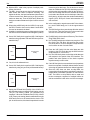
Z16C30 USC®
USER'S MANUAL
ZILOG
USER’s MANUAL
APPENDIX B
QUESTIONS & ANSWERS
USC FAMILY QUESTIONS AND ANSWERS
The following is a compilation of field customer questions
and answers on the USC and IUSC™. They are categorized
in four sections: GENERAL, SERIAL/PROTOCOL, DMA,
and INTERRUPT. These questions and answers are com-
piled on a on-going basis. To get the most updated list of
Q&A’s, call the Zilog Bulletin Board Service (ZBBS) at
(408) 370-8024 via modem (2400-8-N-1-F).
GENERAL QUESTIONS AND ANSWERS
Q: What’s the difference between the three Datacom
support product kits?
A: Here are the main differences between the three
Datacom boards:
Availability
Supports
Plug-In?
Z8018600ZCO
Z16C3001ZCO
ZNW2000
Now
16C30
16C32
16C35
85C30
85230
Now
16C30
Now
16C32
Stand-Alone
Plug-In Card
Yes, ISA Bus
None
Intel
None
Intel
Yes
No
Included
Included
On-Board CPU 80186
CPU Environ.
Intel
Comes With
EPM?
Yes
S/W
Drivers
Included
you can easily refer to the hardcopy of the technical
manual or read directly from the screen. Call the ZBBS
to download your copy of the IUSC Technical Manual
at 408-370-8024. This file is called “IUSC_TM.EXE”
under the “DATACOM SUPPORT” directory. When
executed this file will decompress into separate chapters for easier search. Your customers can also access this ZBBS.
Q: Dynamic ICC means that the part is operating. What is
the speed of operation for this specification, and what
sections of the device are running?
A: Dynamic ICC is specified for the device operating at its
rated speed, with serial transfers and bus activity
occurring as in normal operation. As with all CMOS
devices, the ICC of a USC family device will vary with the
clock speed, with current increasing with increasing
clock rate.
Q: What technology is used to make the USC and IUSC?
A: The USC family is fabricated in an N-well CMOS
technology. The USC and IUSC are currently in 1.6
micron, with the IUSC moving to Zilog’s 0.8 micron
technology in 1994.
Q: How can I use the new USC and IUSC™ technical
manuals more efficiently to debug and answer my
customer’s technical questions?
A: First, have this list of the USC Family Questions &
Answers handy to look-up previously answered questions. This list can be given to the customer for further
analysis. Second, use the index provided with both the
USC and IUSC technical manuals for quick references. Or, for even faster references, an electronic
version of the IUSC technical manual is available on
the ZBBS. Use a text editor to globally search for key
words on the computer. When key words are located,
UM97USC0100
B-1
ZILOG
Z16C30 USC®
USER'S MANUAL
General Questions and Answers (Continued)
Q: New and old samples of the USC act differently when
programmed to interrupt or DMA request when 1 byte
is in the Rx FIFO when used a 16-bit bus. Why?
A: On a 16-bit bus, USCs with data codes of 9136 and
older will interrupt and DMA request when two bytes
are available in the Rx FIFO even when programmed
to request on one byte. This allows the fill level to be
programmed to any level and DMA transfers would be
well behaved. USCs with data codes 9137 and newer
will interrupt and DMA request when one byte is in the
Rx FIFO if so programmed. Therefore, when using
DMA on a 16-bit bus, the Rx DMA request level should
be programmed to request when a minimum of 2 bytes
are available. Otherwise, the DMA will try to transfer a
word when only a byte is valid and cause invalid
characters to be placed in memory.
Q: When reading the Test Mode Data Register (TMDR)
the access time is three times normal. How does this
affect the AC timings?
A: Reading the TMDR (this applies to this register only),
the Data Valid Delay is stretched. This impacts the
following specifications:
#1 Bus Cycle Time
#9 /DS Fall to Data Valid Delay
#33 /RD Fall to Data Valid Delay
#79 /RDY Fall to Data Valid Delay
Q: How are the current state of the /CTS and /DCD pins
monitored using the latch/unlatched command/status
bits?
A: When the Latched/Unlatched status bit in the MISR is
zero, reading the MISR reports the current unlatched
state of the pins. When the Latch/Unlatched bit is set,
the current state of the pin can be found by writing a
one to the latch to clear it and then re-reading the
MISR.
Q: Does the USC family have on-chip protocol processing similar to some other data communications chips?
A: No, Zilog data communication products do not have
on-chip protocol processing. This has not been built
into our chips since it greatly increases die size and,
consequently, cost. Also, many customers report that
they are not able to use the “auto” modes of protocol
processing chips because of their strict limitations on
how they respond...you must make your application
work the way the chip does or you can’t use the chip.
The versatility of the USC family offers a cost effective
solution to adapting chips to meet many application
needs. Next generation products may include integrated CPUs to provide on-chip protocol processing
to meet application needs where appropriate.
B-2
Q: What Application Notes are available?
A: The following Application Notes are available. The
devices each App Note applies to is shown in brackets. Design a Serial Board to Handle Multiple Protocols
[USC ] Using the USC with MIL-STD 1553B [USC,
IUSC] Data Communications with the Time Slot Assigner [IUSC] Using the Zilog Datacom Family with the
80186 CPU [USC, IUSC]
Q: What products does the Electronic Programmer’s
Manual (EPM™) support?
A: There are EPMs available for the USC and IUSC. They
can be purchased from the local Zilog Sales Office or
Zilog distributor.
Q: Should the unused pins of the (I)USC be tied High,
Low, or left floating (i.e., /TxREQ, /CTS, /DCD,...)?
A: The basic rules are: Unused OUTPUT ONLY pins can
be left unterminated. Unused INPUT ONLY pins should
be tied inactive (High if an active Low pin). Unused
I/O pins should use a pull-up (2K typical) to the inactive
state. Users often get tripped up by I/O pins because
they don’t take the time to understand when a pin is an
input and when it is an output. For example, the /SYNC
pin on the SCC family switches from input to output
when programmed for sync modes. This means that
because the SCC resets into async mode, the /SYNC
pin comes up as an input, then when WR4 is programmed, it switches to an output. Consequently,
users can fall into the trap of thinking that because they
are using it in sync mode, it is an output only—but of
course you see the problem is that until programmed,
it is an INPUT!
Q: To what level does the USC family support the Ethernet
protocol?
A: The USC family does support the frame format of
Ethernet, the 10 Mbps speed, and the Manchester
encoding/decoding used. What it does not do is:
address checking of the full 48-bit address (it only
checks 16) nor the collision detection & backoff. This
makes the USC family well suited for internetworking
applications that need the USC family’s multiprotocol
ability, since many inter-net applications (bridges &
routers) have to receive all addresses so that address
checking is not an issue. The USC family is not well
suited to applications that require the full implementation of Ethernet as is done by competitor’s chips which
only do 802.3 (no HDLC) but do support it completely.
These chips are good in LAN adaptors and workstations, but cannot do multiprotocol routing in a single
chip. Note that the USC family will be useful in socalled “full-duplex” Ethernet and point-to-point
Ethernet, since collision detection and back-off is not
used in these cases.
UM97USC0100
Z16C30 USC®
USER'S MANUAL
ZILOG
Q: Which pins are used to perform indirect addressing?
A: Using register pointer addressing, you need one address line for S//D (for the IUSC) or A//B (for the USC)
and one for D//C (i.e. address lines A2 and A1 respectively), so each USC or IUSC takes 4 words or 8 bytes.
0 of the data bus. Similarly, data to be written to the
high order byte (D15-8) should be on AD15-8. Remember, Little-Endian means that the least significant
byte has the lowest address, while Big-Endian means
that the most significant byte has the lowest address.
Q: When reading an 8-bit value on a 16-bit bus from a
USC family register and using a “Big Endian” microprocessor (Motorola 68000), which half of the bus
does the value return on (D15-8 or D7-0)?
A: Regardless of the processor being big or little endian,
the USC family will return an 8-bit value on both halves
of the data bus. When writing an 8-bit value to a
register, the USC family interprets the U//L bit (CCAR:0)
as LittleEndian. Therefore, data to be written to the low
order byte (D7-0) of a register, should be put on AD7-
Q: Is there a problem when using the USC family running
Ethernet on a backplane if minimum node distances
are violated?
A: This question applies to the layer 1 device driver used
and is out of the scope of the Zilog USC family
specification.
SERIAL & PROTOCOL QUESTIONS AND ANSWERS
Q: Does the USC family support a promiscuous receive
(receive all addresses) when using HDLC/SDLC?
A: Yes, this is the default case. No Rx address checking
is selected by programming in the Channel Mode
Register (CMR) bits D5-4=00.
Q: How many FM1 flags are needed to sync up the DPLL
on the USC? Is a flag-to-data transition required to
begin syncing?
A: The DPLL watches the RxD line for transitions. It
assumes that these transitions are either clock or data.
Depending on the position of the transitions within the
bit cell, adjustments are made in the phase of the DPLL
output clock to synchronize this output clock with the
assumed bit cell boundaries of the incoming data.
“Quick Sync” tells the DPLL that the VERY NEXT EDGE
UM97USC0100
it sees is the one to synchronize to; if this is not the case
the DPLL will have to see “n” correct edges before it
will be in sync. This “n” is 3 for X8, 6 for X16, and 12 for
X32. The time required to really get in sync in the worst
case is thus a function of the data encoding method
employed as well as the data on the line during the
process. The key issue is the number of “edges” the
DPLL sees on the RxD line. The DPLL is a feedback
system. It inherently tries to stay in sync. If the DPLL
happens to sync up on the wrong edge, over time it will
adjust to correct the situation, just like it tries to track a
varying input signal. There is no “secret” in this; it
operates just like the SCC DPLL except that it adjusts
a little faster when it’s way out of sync.
B-3
Z16C30 USC®
USER'S MANUAL
ZILOG
SERIAL & PROTOCOL QUESTIONS AND ANSWERS (Continued)
Q: Running asynchronous mode, how do you program a
USC family device to achieve a certain baud rate with
a predetermined external clock? That is, do you need
to use the DPLL, BRG, CTR, or certain encoding
methods?
A: Below are three baud rate and clock rate examples.
The only encoding method allowed for async mode is
NRZ. The DPLL is not used in async mode.
EXAMPLE
BAUD RATE
CLK RATE
DIVISOR
#1
2400
76800
76800/
2400=32
16
64
#2
#3
1M
9600
16M
614400
(1) To achieve : 2400 baud
With ext clk
: 76800 Hz
You need
: 76800 / 2400 = 32X
H/W setup
: RxC pin —> BRG0 —> RxCLK
Set registers: CMR(D13-12)=00 for 16X divisor
TC0R =01h for BRG0 divisor
Validation
: 16X times 2 = 32X
(2) To achieve : 1M baud
With ext clk
: 16 MHz
You need
: 16M / 1M = 16X
H/W setup
: RxC pin —> RxCLK
Set registers: CMR(D13-12)=00 for 16X divisor
TC0R =00h for no divide
Validation
: 16X times 1 = 16X
(3) To achieve : 9600 baud
With ext clk
: 6.144 kHz
You need
: 6.144K / 9.6K = 64X
H/W setup
: RxC pin —> BRG0 —> RxCLK
Set registers: CMR(D13-12)=00 for 16X divisor
TC0R =03h for BRGo divisor
Validation
: 16X times 4 = 64X
Q: When the USC gets an RCC underrun condition, the
device will issue a Device Status Interrupt instead of
the expected Receive Status. What should be done?
A: If the channel ever sets RCCUnder Latched/Unlatched
and interrupts, the processor should clear the condition by writing a 1 to the L/U bit, discard the data
received for the frame(s) by purging the RxFIFO,
reprogram the receive DMA controller if one is being
used, and do whatever else is necessary to clean up
the situation. Then write the “Enter Hunt Mode” command to the RCmd field of the Receive Command/
Status Register (RCSR 15-12)
B-4
Q: Is there a trick to using “Wait2Send” feature?
A: “Wait To Send” works by intercepting the data valid
signal from the FIFO to the transmitter, which has the
effect of stopping transmission at the end of a frame.
This works only when the last byte in the frame is
marked as EOF either explicitly or by using the TCC.
Note that this does not stop DMA requests or interrupt
requests. These signals from the FIFO are not touched
so that data for the next frame will be requested by the
part as soon as the EOF byte is transferred to the
transmitter.
Q: Does CRC16 work the same way as CRC32 in HDLC?
A: In HDLC the CRC is inverted before transmission.
Mathematically this has the effect of forcing a remainder to be present when the CRC calculation is complete. This remainder is a function of the CRC polynomial used, and the USC family is capable of checking
for the proper remainder for the CRC-CCITT polynomial for a 16-bit CRC and the Ethernet polynomial for
a 32-bit CRC. When the CRC-16 polynomial is selected in HDLC mode, it does not work because the
part does not check for the corresponding remainder.
Q: When using multiple USC family devices at separate
stations in HDLC Loop mode, some of the clock jitter
from one station’s receive path onto its transmit path
may increase the error rate. How does the USC family
eliminate this problem?
A: The on-board DPLL will automatically adjust and recover the clock information from the data stream, but
there is no way to eliminate the jitter. At a fundamental
level, the jitter is due to the timing differences between
the local oscillators at the various stations in the loop.
Thus, the limit on the number of stations in the loop, for
error-free transmission, is determined by the local
oscillator tolerance (in nanoseconds), multiplied by
the number of stations in the loop. This product must
be less than one half of a bit time for the loop to function
properly.
Q: What is the maximum bit rate in synchronous mode
with clock recovery from data stream, Manchester
encoding/decoding, and the master clock for USC
family device operating at 20 MHz?
A: Manchester (Biphase-Level) requires the use of the
DPLL. The minimum DPLL divisor is eight, which will
give a data rate of 2.5 Mbit/sec.
Q: Should I use the counters in a USC family device to
have a more stable transmit clock source when I drive
the receiver with the DPLL output?
A: The counters would provide a stable transmit clock
from a common source when the DPLL is providing the
receive clock. The 5-bit counters, which can be programmed to divide an input clock by 4, 8, 16, or 32, can
be used as prescalers for the baud rate generators.
UM97USC0100
Z16C30 USC®
USER'S MANUAL
ZILOG
Q: With the DPLL, what is the purpose of multiple possibilities of divisors?
A: The DPLL is used to recover clock information from a
data stream with NRZI or Biphase encoding. The
higher the divisor, the less instantaneous jitter there is
in the recovered clock. But the price you pay is a lower
maximum data rate. Thus the USC family allows the
designer to trade off data rate for jitter in the recovered
clock.
Q: When using a USC family device in HDLC Loop mode,
the DPLL is used to clock receive data. Can the DPLL
be used to retransmit the data?
A: Certainly, just select the source of the transmit clock as
the DPLL in the Clock Mode Control Register (CMCR).
Q: Can a USC family device perform HDLC half-duplex
transfers using separate TxD and RxD lines (as illustrated below)?
internal receive data input. For the device to receive
data, the TxDMode field (D7-D6) should be set to 01,
selecting the high-impedance state for the TxD driver.
Now, the incoming data from the external device will
be routed to the internal receive data input of the USC
family device. In both cases, the modem hand shaking
signals (/CTS, /DCD) will control who transmits and
who receives.
Q: In the configuration: asynchronous with 7-bits character, can the USC family put 0’s in the upper/unused
bits?
A: The USC family receiver puts the stop bit in the unused
bits of a byte. Thus they are one’s in the normal case
and zero’s in the case of a framing error.
Q: Do USC family devices have a Recovery Time like the
Zilog Z8530 SCC does?
A: No. The USC family does not have a recovery time. The
Bus Cycle Time (AC Spec #1) specifies the access
time of the device. The bus interface is asynchronous
and is similar to that of a static RAM.
TxD
IUSC
Transmission
Facility
RxD
Q: Does the USC family limit the serial data rate with
respect to the CPU clock the way the SCC limits the
serial data rate to 1/4 of PCLK?
A: No. The USC family does not limit the serial data rate
with respect to the speed of the CPU interface. The
parallel and serial portions of the device operate
asynchronously to each other.
A: Yes, this is all software driven.
Q: Can a USC family device perform HDLC half-duplex
transfers by using only one line (as illustrated below)?
TxD
IUSC
Transmission
Facility
Q: Can USC family devices transmit and receive packets
that are composed of multiple chained buffers as well
as having the packets themselves chained together?
A: Since the USC does not have on-chip DMA, the
composition of how the data is organized in memory is
independent of how data is written to or read from the
USC. The IUSC’s on-chip DMA is able to send and
receive messages composed of multiple buffers as
well as terminate a buffer at the end of the message.
RxD
A: Setting the RTMode field (D9-D8) of the CCAR to 10
will allow the system to transmit in half-duplex over the
TxD pin. This mode is called “pin controlled local
loopback”. When the TxDMode field (D7-D6) of IOCR
is 00 (Totem-pole setting) data is transmitted from the
USC family device to an external device via the TxD
pin. At the same time, this data is looped back into the
UM97USC0100
B-5
Z16C30 USC®
USER'S MANUAL
ZILOG
SERIAL & PROTOCOL QUESTIONS AND ANSWERS (Continued)
Q: Is there a minimum length for HDLC/SDLC frames?
A: No, there is no minimum frame length. A frame can be
as short as: Opening Flag, 1 data character, CRC
(optional) and a Closing Flag. If address and control
field handling is specified, the receiver will post Short
Frame status in bit 8 of the RCSR if a closing flag is
received before the control field is complete.
Q: Is the rated serial data rate aggregate, or is the rated
speed for each receiver/transmitter?
A: Zilog specifies the maximum rated serial data rate for
each receiver/transmitter independently (not aggregate).
Q: What is the maximum clock frequency for the Port 0 &
1 pins (IUSC only) when they are used as CLK0 &
CLK1 inputs?
A: The timing requirements for these inputs is the same
as for the /RxC pin.
Q: In HDLC mode, can the USC family do address search
and compare on a 16-bit address?
A: The USC family can check the first 8 bits of the address
field and receive or reject the frame if the incoming
address matches the programmed value (or the global address of FFH).
Q: In HDLC mode, can the extended address/control
feature be used to check for a 16-bit address?
A: The extended address feature allows the device to
extend the point at which it begins to assemble data
according to the programmed character size. It doesn’t
extend the length of the address which is compared
for frame reception or rejection. Extending the address/control field is useful when this field is in 8-bit
increments, but the data is in 7, 6, or 5 bit/char format.
Q: In HDLC mode, does an Abort set the End Of Frame
bit?
A: Yes, an Abort does set the End Of Frame status
(RCSR4), for the last data byte written to the receive
FIFO.
Q: In HDLC mode, does the receiver recognize shared
zero flags as well as non-shared zero flags? Will it
accept shared flags?
A: Yes, the receiver will recognize shared zero flags and
flags shared between frames.
Q: In HDLC mode, will the transmitter send one flag
between frames?
B-6
A: Yes, but only if data is present in the transmit FIFO
when the flag completes transmission. Otherwise another flag or the idle line condition will be started. S26:
In 802.3 mode, is it required to end the frame by
deasserting /DCD?
Q: In 802.3 mode, it is required to end the frame by
deassering /DCD?
A: Yes, it is the deassertion of the /DCD pin that signals
the end of the message in 802.3 protocol. The 802.3
standard provides no other mechanism for terminating a frame. It’s part of the carrier sense in the description of CSMA/CD.
Q: In HDLC mode, is transmitting End Of Frame the same
as Underrun?
A: The End Of Frame (EOF) and Underrun are different
conditions in the USC family. There are register bits
that control the response for each condition separately. This provides for automated response if the
transmitter underruns inadvertently before the intended
end of the frame. The transmitter reaches the Underrun
condition when there is no data to load into the transmit
shift register because the transmit data FIFO is empty.
What the transmitter does in this condition is programmed in the Channel Mode Register (CMR15-14).
The choices are to send either: an Abort (7 1’s), an
extended Abort (15 1’s), a Flag, or accumulated CRC
& Flag. The transmitter reaches the End Of Frame
condition when a byte marked with EOF status is
loaded into the transmit shift register. A byte can be
marked with EOF status in two ways: using the command “Set EOF/EOM” (TCSR15-12=1111), or when
the transmit character counter value reaches zero.
When the TxCRCatEnd bit in the TMR is set to one, the
byte marked with EOF status will be followed by CRC
and Flag.
Q: When the Receive Character Count (RCC) FIFO overflows (it is four entries deep), when is the RCC FIFO
overflow status bit (RCCF Ovflo) CCSR15 set?
A: The USC family sets the RCCF Ovflo bit is set in the
RCC FIFO for the fourth RCC FIFO entry when it
overwrites the previous fourth entry in the RCC FIFO.
The first three entries do not have the overflow status
set. Once the first three entries in the RCC FIFO are
read, the overflow bit will be set in the CCSR. The
overflow status is only cleared by writing a 1 to the
“Clear RCC FIFO” bit (CCSR13). This also empties the
RCC FIFO and clears the RCC FIFO Available bit.
UM97USC0100
Z16C30 USC®
USER'S MANUAL
ZILOG
Q: Does the Purge Rx FIFO command clear the Receive
Character Counter?
A: No, the Purge Rx FIFO command does not clear the
Receive Character Counter, but it does cause the
contents of the RCLR to be loaded into the receive
character counter.
Q: What are the wiring concerns when connecting multiple IUSCs together?
A: Unless addresses are multiplexed onto the AD pins
with data, don’t connect the /AS pins of the IUSC’s to
any signal from or derived from the processor or
backplane bus. Instead connect them all together and
connect a pullup resistor to keep the line high when the
CPU has control of the bus.
The decoding logic that drives /CS should ensure that
no IUSC’s /CS pin can go low when another IUSC is in
control of the bus. Also the /INTACK pins must stay
high when an IUSC is in control of the bus.
Always connect all of the /UAS and /AS pins of the
IUSC’s together and use them to latch addresses from
the AD15-0 lines. Put a pullup resistor on /UAS to keep
the line high when the CPU has control of the bus.
Either connect all of the /DS pins together or all of the
/RD and /WR pins, but not all three. If all three are
interconnected, the first time one of the IUSCs becomes bus master and drives /DS and /RD or /DS and
/WR low, it will inactivate all of the other IUSCs. Provide
separate pullup resistors for each of the /DS pins or for
each of the /RD and /WR pins, whichever signals are
not used in the host bus.
Q: Can the /TxC pin be used for both data recovery in the
Rx data stream as well as clocking the transmit data?
A: Typically in this situation, while the DPLL is supplying
the receive clock, one of the counters (CTR0 or CTR1)
will be used to supply a fixed transmit clock at the
same rate. The problem with using the DPLL output to
drive the transmitter is that once the receive data
stream stops, the DPLL output may stop also, depending on the mode. Note that in HDLC Loop applications
it is necessary to use the DPLL outputs to drive both the
receiver and transmitter to prevent bit errors due to
timing differences between the different stations on
the loop.
Q: When using the USC family in 16-bit multiplexed mode
and directly addressing the transmit and receive data
registers, is it necessary to use the D//C pin?
A: No, on the USC in multiplexed mode, one would tend
to ground the D//C pin. But do not carry this idea over
to IUSC applications, in which D//C is needed to select
between the DMA channels for access to their (nonshared) registers.
Q: Why is the following General Timing specified:
T3 TsTxd(RxCf) RxD to /RxC Fall Setup Time?
T4 ThRxD(RxCf) RxD to /RxC Fall Hold Time?
A: For NRZ, NRZB, NRZI-Mark and NRZI-Space
encodings, these specifications are not applicable.
However, for all of the Biphase encodings, where the
receive data signal may change on both edges of the
clock, the receiver must sample the RxD pin on both
edges of the clock. Hence these two specifications.
Q: Can any data encoding method be used in Async
mode?
A: No, only NRZ can be used, for the simple reason that
in Async the receiver is looking for a 1-to-0 transition to
start the counting of receiver clocks to do the X16, X32
or X64 clock dividing. NRZ is the only encoding
method that can guarantee this edge polarity for a start
bit.
Q: How many receive clocks are required after the clock
that samples the last zero in a closing Flag to get the
last byte of data into the receive FIFO?
A: Three receive clocks, after receipt of the closing Flag,
are required to get the last byte of data into the receive
FIFO.
Q: What can cause the receiver to miss generating
RxBound interrupts? Depending on the FIFO Request
Level, the RxBound interrupt seems to be missing on
either odd-length or even-length frames.
A: The software is not setting the WordStatus bit in the
RICR. What happens is that the interrupt logic is then
seeing only the status on one byte when a word is read
from the receive FIFO. This leads to missing status
interrupts.
Q: When using data encoding, the USC family specifies
the /TxC to TxD output delay at 35 ns max., for both
rising and falling edge of clock. What is the maximum
expected difference between /TxC rise to TxD out and
/TxC fall to TxD out.
A: These two delay times are matched very closely for
any specific device, due to the inherent matching
within a semiconductor device.
UM97USC0100
B-7
Z16C30 USC®
USER'S MANUAL
ZILOG
SERIAL & PROTOCOL QUESTIONS AND ANSWERS (Continued)
Q: The Transmit Control Block is being sent as data. What
am I doing wrong?
A: If the previous transmit frame ended normally, the TSB
is automatically routed to the proper registers in the
USC family. However, if you are starting up, or pro-
cessing a case where the previous frame did not
terminate normally (because of an underrun, for example) it is necessary to condition the transmitter to
expect a TSB instead of data. The Load TCC command in the CCAR is the easiest way to do this. Refer
to the Technical Manual for more details.
DMA QUESTIONS AND ANSWERS
Q: While in the master mode using the IUSC, what is the
timing of the Byte/Word signal?
A: B//W has the same timing as S//D and D//C. When the
IUSC is transferring a byte the signal is High; when the
IUSC is transferring a word the signal is Low.?
Q: The IUSC Spec shows the Memory Read timing diagram. If the DMA is in the middle of one of these cycles,
the memory is driving the data bus while /RD is low.
/RD will go high 25 nsec max after the falling edge of
CLK (param. 141). If the next DMA cycle begins on the
next rising CLK edge, then the DMA will come out of tristate and drive the bus with the address 25 nsec max
after the rising edge of CLK. With a 16 MHz DMA clock,
about 30 nsec of CLK-low time exists. Going strictly
from the numbers given, param 141 could be 25 nsec
exactly, while param 148 could be close to zero nsec.
This would give the memory only about 5 nsec in which
to go tri-state before the DMA began driving the bus
with the address (30 nsec CLK-low time minus 25 nsec
for /RD to go high plus 0 nsec possible for the DMA to
begin driving the bus after CLK goes high).
Can you provide a more realistic number to use
(/RD-high to-ADbus-being-driven)? Is the next cycle
really going to begin at the last rising edge (i.e., is the
last rising CLK edge the same as the first rising CLK
edge shown on the page)?
A: Yes, the next rising edge of CLK will start another DMA
cycle. However, parameter #145 has been modified to
also carry a minimum value. This is because on a
single chip one cannot have one delay time that is at
the maximum while another delay time is at the minimum; the two numbers will track. This gives the designer much more than the 5 ns that you cite above
B-8
Q: Is there a mode where the USC can deassert the
/DMAREQ pin without using the /DMAACK (that is,
/TxACK & /RxACK)?
A: This is just a flow through DMA transfer, which is
supported by the USC. The DMA controller performs
two bus cycles for each piece of data transferred
between the USC and memory. The first cycle reads
data from the source, be it the USC or the memory. The
DMA controller captures this read data and then
presents it on the data bus again in the second cycle
which is a write to memory if the data came from the
USC or a write to the USC if the data came from
memory. The main advantage of flowthrough transfers
is that they involve minimal hardware design considerations, because both cycles of each pair are similar to
bus cycles performed by the host processor. The
/RXREQ and /TxREQ signals will be deasserted during the bus cycle just as if /RxACK or /TxACK were
being used to transfer the data. The /TxACK and
/RxACK pins can be used as outputs or as polled
inputs in this case.
Q: What’s the largest memory buffer possible when using
the array or linked list mode in the IUSC? In which
register is it programmed?
A: The length of the buffer is programmed in the relevant
Byte Count Register. Since these registers are 16-bits
wide, there is a 64K byte limit on the size of buffers.
Q: When using the IUSC, what is the minimum time
between /BUSREQ active and /BIN active?
A: There is no particular timing requirement or relationship between /BUSREQ and /BIN. The IUSC is always
ready to deal with a falling edge on /BIN. If it is
requesting the bus, it keeps /BUSREQ asserted while
it uses the bus, which lasts until it doesn’t have anything more to do, or its usage is limited by the BDCR,
or /BIN goes high or /ABORT goes low. If it doesn’t
want to use the bus it drives /BOUT low for as long as
/BIN stays low.
UM97USC0100
Z16C30 USC®
USER'S MANUAL
ZILOG
Q: Can an IUSC DMA channel that was terminated by
/ABORT or /BIN going active or inactive, respectively,
resume transfers where it stopped?
A: If the DMA transfer is stopped by negation of /BIN, the
IUSC will assert /BUSREQ again automatically, as
soon as 8 or 40 clocks have gone by per MinOff39
(DCR5). Then when the processor or arbiter answers
with /BIN the DMA will start up exactly where it left off.
If the DMA transfer is stopped by the assertion of
/ABORT, the BUSY bit is cleared, so the DMA channel
won’t do anything again until the software sets it again
by means of one of the Start commands. Software
controls whether this restart is “in place” (Start or Start/
Continue), or whether it drops back to the start of a
memory buffer (Start/Init).
Q: In HDLC mode using DMA, can the USC notify the CPU
when a closing flag is encountered by the receiver
before the fill level is reached by using a pin?
A: When programmed as a DMA request, the /RxREQ pin
goes normally active when the FIFO reaches the fill
level. This function is enabled by setting the CCAR
(D15-D11) for “receive DMA request.” The
/RxREQ signal will also go active when the receiver
writes the last byte before the closing Flag of a received message into the Rx FIFO.
Q: Why is DMA transmit request, /TxREQ, asserted before the transmitter is enabled?
A: The DMA request signals are independent of the
transmit and receive logic. Therefore, if the transmit
FIFO is below the programmed fill level, /TxREQ will go
active independent of the transmitter being enabled.
This is typical when first starting up a channel since the
FIFO is empty when /TxReq is enabled.
Q: When using the IUSC on a 16-bit bus, how is the last
byte transferred to memory if the there are an odd
number of bytes in the received message? Is there a
mechanism to handle this?
A: In serial protocols which result in the IUSC setting the
RxBound bit in the RCSR (HDLC, 802.3, 1553B, NBIP,
External Sync, Transparent Bisync) the byte with
RxBound status set will be transferred to memory
regardless of its byte/word boundary in the received
message. The Rx DMA will continue to request transfers until the character with RxBound status is moved
to memory. When only one byte remains in the Rx
FIFO, the Rx DMA will complete a 16-bit transfer to
memory. The fact that only one byte of the transfer is
valid is indicated by the 1stBE (RCSR14), or by the odd
value of the Receive Character Count (RCC).
UM97USC0100
Q: When the DMA in the IUSC reads external memory for
array or linked-list table information, does it attempt to
fetch all bytes in one burst access or does it release the
bus between byte/word accesses?
A: The IUSC will attempt to move all the bytes in one
access. Of course, if the transfer is interrupted or
aborted, subsequent transfers will be required.
Q: In the IUSC in array and linked-list modes and in the
event of a receive CRC error, is the current receive
buffer reused?
A: No, buffers are not re-used when a CRC or any other
error is detected. A buffer is only re-used when its
address is explicitly given to the DMA a second time.
Q: When using array or linked list modes in the IUSC, can
several chained data buffers be sent in one frame, or
is CRC and closing Flag sent at the end of each buffer?
A: Yes, multiple memory buffers can be sent in one frame.
The IUSC provides features which allow the data
buffer boundaries to be independent of serial data
packet boundaries. The IUSC uses separate counters
for the size of the memory buffer and the size of the
frame (TCLR). The best way to use the TCLR is to use
the Transmit Control Block (TCB) feature (CCR bits
D15 & D14). By putting the size of the packet in
memory in the TCB, the frame length value will automatically go to the Transmit Count Limit Register
(TCLR) and will cause the CRC and Flag to be appended after this number of bytes has been transmitted, independent of DMA buffer boundaries.
Q: When does the IUSC release the bus relative to
/BUSREQ going inactive?
A: /BUSREQ is driven high from the same rising edge on
CLK at which it releases the various other bus signals.
This is shown in the IUSC Technical Manual under
“Bus Acquisition and Release Timing”.
Q: What is the function of the S//D and D//C pins when the
IUSC is bus master?
A: The S//D and D//C pins can be configured to output the
type of DMA access that is in progress. If these pins
are configured as inputs only, they are ignored during
the DMA transfers and the system should always drive
them.
Q: When using Receive Status Block with 16-bit DMA
transfers and a odd number of data bytes is received,
will the status block be transferred to memory on odd
or even memory addresses?
A: The data transfer which moves the last byte of data is
still a word transfer of which only one byte is valid.
Therefore, the status block (or next data) will be to an
even addresses.
B-9
ZILOG
Z16C30 USC®
USER'S MANUAL
DMA QUESTIONS AND ANSWERS (Continued)
Q: Since the Receive Status Block is appended to the end
of the data in memory, how does software determine
where the last byte of data is?
A: Rather than using a two word status block, use a one
word status block and then read the RCCR register for
the byte count of the frame. This register is FIFO’d four
deep to allow the system latency in reading out this
value. An alternative solution is to fill the memory buffer
with a known pattern when starting and find where the
pattern stops to determine how many bytes are in the
frame. The IUSC has a new feature that enables the
DMA to write the Receive Status Block as part of the
array table in array mode or as part of the linked-list in
linked-list mode.
Q: The Technical Manual shows that /BUSREQ is driven
high 4.5 clocks after the rising edge of the strobe for
that last transfer. The specification is stated as a
minimum. What is the maximum?
A: The /BUSREQ signal drives high 4.5 clocks after the
strobe. This specification can be considered both a
min and max; the delay is always 4.5 clocks.
Q: The IUSC AC specification #148 shows the maximum
active delay for the data bus after the rising edge of
clock. What is the minimum?
A: The minimum is 0 ns The IUSC can begin to drive the
address immediately after the rising edge of clock. A
delay of 15 ns would be typical.
Q: Why does the IUSC insert inactive states after a bus
transfer without releasing bus control?
A: The ‘inactive’ states are used by the IUSC to update
the internal device status to determine if the bus
should be released. For example, after completely
filling the transmit FIFO, it is necessary to determine if
the receive channel needs to move data and, therefore, continue to hold mastership of the bus. Another
example of an ‘inactive state is the time between
fetching the link address pointer and the fetching the
link address in linked list mode.
Q: Is there a signal that can be used as a ‘pre-warning’ of
the removal of the /BUSREQ signal? Is there a method
to reduce the number of clock cycles between the last
transfer to the deassertion of BUSREQ?
A: There is no signal to indicate the deassertion of
/BUSREQ. There is no known way to shorten the bus
release time. The 4.5 clocks to release the bus is a
small overhead to the total time for data transfers.
B-10
Q: What is the advised sequence of register access to
initialize the DMA controller in the IUSC?
A: There is a chapter in the IUSC Technical Manual which
provides guidelines on the requirements for programming sequence. Those used to the SCC will find the
IUSC much less sensitive to programming sequence.
Q: What is the advised sequence of register access in
starting and continuing array chained DMA operation?
Are there any tricks to do this?
A: Once a DMA channel is initialized and enabled, continuous operation is automatic. It is recommended to
always maintain a link entry with a byte count of zero.
This will prevent the IUSC from accessing memory in
unexpected places if buffer processing falls too far
behind the serial data. The only trick to keeping the
DMAs going is for the memory management software
to keep ahead of the serial channel’s usage of memory
buffers.
Q: In linked-list mode, what is the maximum number of
links in the chain?
A: There is no maximum number of buffers that can be in
the linked list. The size of the linked list is only limited
by the size of system memory and memory management software.
Q: In Linked List or Array mode, is there a method to
determine that a buffer has been started and completed?
A: The IUSC DMA channel can indicate that a buffer has
started use by enabling the Ring Buffer feature
(TDMR12 or RDMR12 set to 1). When the DMA channel
reads the buffer byte count, it will write back the count
value as zero. Therefore, software can check this word
to see that if the byte count is zero, the buffer count has
been read. Completion of the buffer can be easily
determined by enabling the Linked Status Transfer
feature (TDMR13 or RDMR13 set to 1). With this feature
enabled the Array and Linked List entries have an
unused word following the control/status words. This
unused word is written with zero’s when a buffer is
completed. Therefore, if this word is written with any
non-zero value when the array or list is set up, buffer
completion can be determined by checking this word.
UM97USC0100
Z16C30 USC®
USER'S MANUAL
ZILOG
Q: Are there some rules of thumb to tune the device for
performance problems?
A: If you are experiencing RCC FIFO overflows, try increasing the Rx DMA Trigger Level. This has the effect
of diminishing the overhead of DMA transfers on the
bus, which may give more bandwidth to the processor
for handling the End Of Frame condition. A less desirable alternative is to increase the number of bytes per
frame, which reduces the bandwidth required for
handling the End Of Frame condition.
If you are experiencing Rx FIFO overruns with interrupts, either decrease the Rx FIFO Interrupt Level if the
overflow is occurring as a result of long interrupt
latency, or increase the Rx FIFO Interrupt Level if the
overflow is occurring as a result of processing during
the interrupt service routine. If the overruns are occurring with DMA operation, decrease the Rx DMA Trigger Level to better account for bus latency.
If you are experiencing Tx FIFO underruns with interrupts, either decrease the Tx FIFO Interrupt Level if the
underrun is occurring as a result of long interrupt
latency, or increase the Tx FIFO Interrupt Level if the
underrun is occurring as a result of processing during
the interrupt service routine. If the underruns are
occurring with DMA operation, decrease the Tx DMA
Trigger Level to better account for bus latency.
Remember that when talking about levels in the FIFO,
the CPU sees the Rx side as the number of slots filled
and the Tx side as the number of slots available.
Q: While using the IUSC, the transmitter sends all data
correctly. The Rx DMA will receive bad data on every
other byte. Also the /RxREQ signal will change states
on every other byte. What is this a symptom of?
A: When using 16-bit DMA transfers, the DMA request
level values in the RICR must always be programmed
to at least 1, indicating 2 bytes received in the RxFIFO.
Similarly, the TICR must always be programmed to at
least 1, indicating 2 empty bytes in the TxFIFO. Otherwise the serial channel will request what the DMA
thinks is a word transfer for every byte.
Q: Does the Master Bus Request Enable bit (MBRE) in the
DCAR need to be “1” when doing register pointer
writes to the DCAR (for non-multiplexed slave accesses)?
A: When using indirect register addressing, software
typically should include a “1” in the MBRE bit when
writing a register address to the DCAR. If MBRE is
cleared when writing a register address to the DCAR,
the DMA channels are thereafter prevented from requesting and using the bus to transfer data to or from
the serial channel.
Q: Is it possible to use the Receive status block in basic
asynchronous mode? The customer wants to put each
received character by DMA in memory associated
with a status word.
A: No, both receive status blocks and transmit control
blocks only apply to “framed” protocols like HDLC.
Storing a status word with each byte can be done by
reading the RCSR before each data byte. Just read the
status before the data. This would have to be done
under interrupt control as a DMA would only pick up
the data.
Q: Is it possible to simultaneously use interrupts and DMA
to receive characters?
A: Yes, because the DMA and interrupt request thresholds are programmed independently. Therefore, you
could interrupt on a fill level of 2 bytes, but DMA
request on 16. Such a scheme is fraught with perils, as
it may happen that the CPU and DMA could inadvertently interleave FIFO reads. A better use of the DMA
request would be for some higher priority interrupt
since the normal interrupt had not yet been serviced.
After programming the DMA request threshold, it is
good programming practice to write the TCSR or
RCSR to select the FIFO Fill Level, to prevent software
from inadvertently modifying the Interrupt or Request
Levels in the TICR or RICR.
UM97USC0100
B-11
ZILOG
Z16C30 USC®
USER'S MANUAL
DMA QUESTIONS AND ANSWERS (Continued)
Q: Why is the /BIN input sampled twice in the IUSC?
/BIN is a bus grant, and if /BUSREQ is sent, why should
more than one bus grant be required? It would appear
that at the end of a transfer, /BIN goes high early
enough so that a device does not become confused
by the /BIN being low for another device’s transfers.
A: This allows the arbitration mechanism to present a
high-performance but, occasionally, metastable grant
to the IUSC. The IUSC takes a while to get the state
machine going. And these start-up steps occur between the two samples. You can view at the second
sample as a confirming one, just before the IUSC starts
active operation.
Q: My system sometimes locks up after trying to add
entries to a Linked List. What is going on?
A: The most likely cause is an interlock problem with the
process and DMA accessing the byte count in the last
entry in the List. There is a specific way to add entries
to the List under these circumstances. It is detailed in
the IUSC Technical Manual.
INTERRUPT QUESTIONS AND ANSWERS
Q: When does the /W//RDY signal go tri-state?
A: The /W//RDY never goes tri-state as an output, but is
only driven High or Low. When acting as an input, its
AC characteristic is the same as a tri-stated output. As
stated in the Tech Manual, if several devices are in the
board, the hardware must logically combine the
/W//RDY pins. In the IUSC the /W//RDY pin is released
from the driven condition (goes tri-state at the same
time that the bus control signals are driven by the
IUSC. In a similar fashion, the /W//RDY pin is returned
to a driven state when the bus controls are tri-stated by
the IUSC. This pin will always return High; it only goes
Low in response to some kind of bus cycle. For Wait
mode it only goes Low during interrupt acknowledge
cycles, and in Ready mode it goes Low for any access
of the IUSC as a slave.
Q: Why is it necessary to disable interrupts (as with the
SCC) to do address demultiplexing from data?
A: It is prudent to disable interrupts when doing the
“address point” operation because if the pointer is
pointing at an address and an interrupt for that channel
comes, the service routine will disrupt the pointer and
then return to the main program without restoring the
pointer, which will disrupt the USC’s normal operation.
Note that because the USC contains a pointer per
channel, only the channel being “pointed to” needs to
have its interrupts disabled.
Q: When an overrun condition occurs, will the USC continue to assert the DMA request until the FIFO is
purged, or will the DMA request be disabled after the
maximum number of characters specified by initial
value of RCLR have been transferred out of the Rx
FIFO (that is in case the Rx FIFO is not able to be
purged in time)?
B-12
A: When the overrun data enters the Rx FIFO, the USC will
not recognize it until it reaches the top of the Rx FIFO.
The DMA will continue to transfer data until the overrun
data reaches the top of the Rx FIFO. Then the overrun
interrupt is generated and the recovery process begins with software.
Q: Why and when should an Interrupt Pending (IP) bit be
cleared?
A: IP bits should be cleared so that another incoming
interrupt can be requested while the current interrupt
is serviced. IP bits can be cleared at the beginning or
the end of the interrupt routine.
Q: An abort is received on the 4th byte in the middle of a
Rx frame. Is abort marked after the 3rd byte?
A: The fourth byte is tagged with both RxBound and Abort
if the Abort Frame option is programmed in the RMR.
Otherwise the Abort condition is reported immediately
and the software must read out the Rx FIFO until the
RxBound byte is found, checking the CRC results at
the same time.
Q: What happens if the received frame is shorter than the
programmed Rx Interrupt or Rx Request Level? Will
the USC family request any kind of interrupt or DMA
transfer?
A: The USC family will request an Rx data interrupt when
the byte tagged with RxBound is written into the FIFO.
In the interrupt routine, one must check the number of
bytes in the Rx FIFO. Read those bytes out of the FIFO.
When the byte tagged with RxBound is the oldest byte
in the FIFO, the USC will request a Rx Status interrupt.
(The Rx Stat IP in the DCCR will be set, and the
RxBound bit in the RCSR will be set).
UM97USC0100
ZILOG
Q: The IUSC Technical Manual states that /DS and
/INTACK should never be active at the same time.
However, the nonmultiplexed Interrupt Acknowledge
Cycle timing diagram shows both of these pins active
at the same time.
A: The manual states that no two strobe signals should be
active at the same time. In the case of Status Interrupt
Acknowledge cycles, the /INTACK pin is a status
signal and the /DS pin is the signal that strobes the
interrupt vector. This is different from the case of the
Pulsed or Double-Pulsed Interrupt Acknowledge cycle
where the /INTACK pin is strobing in the interrupt
vector.
Q: Explain why sometimes the reading on the fill level of
the receive FIFO reports that there are 33 bytes in a 32
byte deep FIFO?
A: When the receive FIFO is overrun, it can read that there
are 33 bytes available. This is due to the fact that there
is a holding register where data is held before being
put into the receive FIFO (this allows status like RxBound
to be marked with the data when it loaded to the FIFO).
When the receiver overruns it stops receiving data.
When the last byte of data is transferred to memory, a
Rx Status interrupt is generated (the interrupt is triggered by removing the byte with overrun status). The
Rx FIFO Purge command is necessary to clear the
overrun and re-enable receiving data. It may be desirable to also issue the command “Enter Hunt Mode” (in
the RCSR register) so that reception starts at the
beginning of the next frame.
Z16C30 USC®
USER'S MANUAL
Q: If multiple interrupts occur, how many can the IUSC
queue up?
A: There are 30 interrupt sources in the IUSC, divided into
six types in the Serial section and eight DMA interrupt
sources (4 of each type per channel). Each source is
individually maskable; those that are armed and enabled are ORed together to assert the single /INT pin.
When the CPU acknowledges the interrupt, the IUSC
tells the CPU which is the highest priority type that is
enabled and requesting. If all 8 types were requesting,
I suppose you could say that the lower 7 types were in
some sense queued. For some of the sources that
involve edge detection, such as the modem control
pins, there’s a more meaningful answer. As noted in
the “Edge Detection and Interrupts” section of IUSC
Technical Manual, there is a hidden edge detection
latch that can record another edge of the same polarity
before software has finished handling the previous
edge of that type. So for these sources the answer is
“the IUSC can queue a second interrupt for some
sources, besides the one it’s requesting for”.
Q: When should the Sent bits (i.e. EOF/EOM Sent, CRC
Sent, All Sent) in the TCSR be reset during an interrupt
service routine?
A: As stated in the IUSC Technical Manual, software
should clear or unlatch status register bits after clearing IP and before clearing and rearming the IA bits.
Q: When the IUSC is operating in Linked List mode with
Early Buffer Termination and the End Of Buffer (EOB)
is reached somewhere in the last buffer, what is the
sequence of setting EOB and EOL? Does the EOL bit
get set at the same time as the EOB bit, or will the EOB
become set first, and the EOL become set second
after the DMA tries to fetch the next link?
A: The EOB bit is set during the clock cycle between the
last buffer access and the first array fetch. The EOL bit
is set during the clock cycles immediately after the
array fetch which reads the zeros in the buffer length
field, indicating no more buffers. Under normal circumstances the CPU servicing the EOB interrupt will
see both of the bits set at the same time, but if the DMA
releases the bus before fetching the array entry, and
the CPU is able to read the status bits during this time,
only the EOB bit will be set.
UM97USC0100
B-13
Z16C30 USC®
USER'S MANUAL
ZILOG
© 1997 by Zilog, Inc. All rights reserved. No part of this document
may be copied or reproduced in any form or by any means
without the prior written consent of Zilog, Inc. The information in
this document is subject to change without notice. Devices sold
by Zilog, Inc. are covered by warranty and patent indemnification
provisions appearing in Zilog, Inc. Terms and Conditions of Sale
only. Zilog, Inc. makes no warranty, express, statutory, implied or
by description, regarding the information set forth herein or
regarding the freedom of the described devices from intellectual
property infringement. Zilog, Inc. makes no warranty of merchantability or fitness for any purpose. Zilog, Inc. shall not be
responsible for any errors that may appear in this document.
Zilog, Inc. makes no commitment to update or keep current the
information contained in this document.
B-14
Zilog’s products are not authorized for use as critical components in life support devices or systems unless a specific written
agreement pertaining to such intended use is executed between
the customer and Zilog prior to use. Life support devices or
systems are those which are intended for surgical implantation
into the body, or which sustains life whose failure to perform,
when properly used in accordance with instructions for use
provided in the labeling, can be reasonably expected to result in
significant injury to the user.
Zilog, Inc. 210 East Hacienda Ave.
Campbell, CA 95008-6600
Telephone (408) 370-8000
Telex 910-338-7621
FAX 408 370-8056
Internet: http://www.zilog.com
UM97USC0100