1
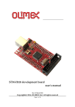
STM32-H107 development board
Users Manual
All boards produced by Olimex are ROHS compliant
Rev. C, June 2011
Copyright(c) 2011, OLIMEX Ltd, All rights reserved
Page1
INTRODUCTION
STM32-H107 header board provides easy way for developing and prototyping with
the new STM32F107VCT6 connectivity line microcontroller, produced by
STMicroelectronics. STM32-H107 has JTAG port for programming and debugging,
USB_OTG, user button, two status leds, and most of the GPIOs are on extension
headers where you can connect your additional circuits.
BOARD FEATURES
-
CPU: STM32F107VCT6 32 bit ARM-based microcontroller with 256 KB Flash,
64KB RAM, USB OTG, Ethernet, 10 timers, 2 CANs, 2 ADCs, 14 communication
interfaces
-
JTAG connector with ARM 2x10 pin layout for programming/debugging
-
25 Mhz crystal
-
USB_OTG
-
Power Jack
-
WKUP button
-
RESET button
-
Two status leds
-
Power-on led
-
3V battery connector
-
Extension port connectors for many of microcontrollers pins
-
PCB: FR-4, 1.5 mm (0,062"), soldermask, silkscreen component print
-
Dimensions: 70x50mm (2.76x1.97")
ELECTROSTATIC WARNING
The STM32-H107 board is shipped in protective anti-static packaging. The board
must not be subject to high electrostatic potentials. General practice for working
with static sensitive devices should be applied when working with this board.
BOARD USE REQUIREMENTS
Cables: The cable you will need depends on the programmer/debugger you use. If
you use ARM-JTAG, you will need LPT cable, if you use ARM-USB-OCD, or ARMUSB-OCD-H, you will need RS232 cable and 1.8 meter USB A-B cable and if you
use ARM-JTAG-EW, ARM-USB-TINY, or ARM-USB-TINY-H, you will need 1.8
meter USB A-B cable.
Hardware: Programmer/Debugger – one of the Olimex ARM Programmers: ARMJTAG, ARM-USB-OCD ARM-USB-OCD-H, ARM-USB-TINY, ARM-USB-TINY-H,
ARM-JTAG-EW.
Software: ARM C compiler and JTAG programmer.
Note: For OpenOCD we don't offer any projects.
Page2
PROCESSOR FEATURES
STM32-H107 board use ARM-based 32-bit microcontroller STM32F107VCT6 with
these features:
–
–
–
–
–
Core: ARM 32-bit Cortex™-M3 CPU
–
72 MHz maximum frequency, 1.25 DMIPS/MHz (Dhrystone 2.1)
performance at 0 wait state memory access
–
Single-cycle multiplication and hardware division
Memories
–
256 Kbytes of Flash memory
–
64 Kbytes of SRAM
Clock, reset and supply management
–
2.0 to 3.6 V application supply and I/Os
–
POR, PDR, and programmable voltage detector (PVD)
–
25 MHz crystal oscillator
–
Internal 8 MHz factory-trimmed RC
–
Internal 40 kHz RC with calibration
–
32 kHz oscillator for RTC with calibration
Low power
–
Sleep, Stop and Standby modes
–
VBAT supply for RTC and backup registers
2 × 12-bit, 1 µs A/D converters (16 channels)
–
Conversion range: 0 to 3.6 V
–
Sample and hold capability
–
Temperature sensor
–
up to 2 MSps in interleaved mode
–
2 × 12-bit D/A converters
–
DMA: 12-channel DMA controller
–
–
–
Debug mode
–
Serial wire debug (SWD) & JTAG interfaces
–
Cortex-M3 Embedded Trace Macrocell™
80 fast I/O ports
–
–
Supported peripherals: timers, ADCs, DAC, I2Ss, SPIs, I2Cs and
USARTs
80 I/Os, all mappable on 16 external interrupt vectors and almost all 5
V-tolerant
10 timers
Page3
–
–
–
four 16-bit timers, each with up to 4 IC/OC/PWM or pulse counter and
quadrature (incremental) encoder input
–
1 × 16-bit motor control PWM timer with dead-time generation and
emergency stop
–
2 × watchdog timers (Independent and Window)
–
SysTick timer: a 24-bit downcounter
–
2 × 16-bit basic timers to drive the DAC
14 communication interfaces
–
2 × I2C interfaces (SMBus/PMBus)
–
5 USARTs (ISO 7816 interface, LIN, IrDA capability, modem control)
–
3 SPIs (18 Mbit/s), 2 with a multiplexed I2S interface that offers audio
class accuracy via advanced PLL schemes
–
2 × CAN interfaces (2.0B Active) with 512 bytes of dedicated SRAM
–
USB 2.0 full-speed device/host/OTG controller with on-chip PHY that
supports HNP/SRP/ID with 1.25 Kbytes of dedicated SRAM
–
10/100 Ethernet MAC with dedicated DMA and SRAM (4 Kbytes):
IEEE1588 hardware support, MII/RMII available on all packages
CRC calculation unit, 96-bit unique ID
Page4
BLOCK DIAGRAM
Page5
MEMORY MAP
Page6
SCHEMATIC
3.3V
+5V
JTAG
+5V_JTAG
10k
R27
10k
10k
R29
R30
R28
10k TDO
RST
R-T
2
1 TRST
R1
3
2
1
3.3V_MCU_E
PB2/BOOT1
100nF C5
100nF C4
100nF C3
100nF C2
100nF C1
10
27
99
74
49
L1
22
C7
100nF
+
F B0805/600R/200mA(201209-601)
C6
10uF/6.3V/TANT
19
VDD
VDD
VDD
VDD
VDD
R3
C8
100nF
C9
NA
21
20
0R(NA)
0R
3.3V
3.3V
VSS
VSS
VSS
VSS
VSS
VDDA
100nF
2.2uF/6.3V
VREF+
VREF-
6
R4
HN1x3
0
94
10k
VBAT
B0_1/B0_0
C10
27pF
12
R5
NA
Q1
Q25.000MHz/HC-49SM(SMD)/20pF
C11
27pF
R6
13
150R
RST
EXT2-37
EXT2-36
EXT2-35
EXT2-34
EXT2-33
EXT2-32
EXT2-31
EXT2-30
EXT1-7
EXT1-8
EXT1-9
EXT1-10
EXT1-11
EXT1-12
EXT1-13
EXT1-14
33k
0R(NA)
R35
22R
R36
22R
C26
C27
100nF
47pF(NA)
OTG_DM
OTG_DP
C28
47pF(NA)
OTG_ID
USB_OTG
PC0/ADC12_IN10
PC1/ADC12_IN11/ETH_MII_MDC/ETH_RMII_MDC
PC2/ADC12_IN12/ETH_MII_TXD2
PC3/ADC12_IN13/ETH_MII_TX_CLK
PC4/ADC12_IN14/ETH_MII_RXD0/ETH_RMII_RXD0
PC5/ADC12_IN15/ETH_MII_RXD1/ETH_RMII_RXD1
PC6/I2S2_MCK/TIM3_CH1
PC7/I2S3_MCK/TIM3_CH2
PC8/TIM3_CH3
PC9/TIM3_CH4
PC10/UART4_TX/USART3_TX/SPI3_SCK
PC11/UART4_RX/USART3_RX/SPI3_MISO
PC12/UART5_TX/USART3_CK/SPI3_MOSI
PC13/TAMPER-RTC
PC14/OSC32_IN
PC15/OSC32_OUT
BOOT0
3
2
1
1
2
C24
PB0/ADC12_IN8/TIM3_CH3/ETH_MII_RXD2/TIM1_CH2N
PB1/ADC12_IN9/TIM3_CH4/ETH_MII_RXD3/TIM1_CH3N
PB2/BOOT1
PB3/JTDO/SPI3_SCK/TRACESWO/TIM2_CH2/SPI1_SCK
PB4/JNTRST/SPI3_MISO/TIM3_CH1/SPI1_MISO
PB5/I2C1_SMBAL/SPI3_MOSI/ETH_MII_PPS_OUT/ETH_RMII_PPS_OUT/TIM3_CH2/SPI1_MOSI/CAN2_RX
PB6/I2C1_SCL/TIM4_CH1/USART1_TX/CAN2_TX
PB7/I2C1_SDA/TIM4_CH2/USART1_RX
PB8/TIM4_CH3/ETH_MII_TXD3/I2C1_SCL/CAN1_RX
PB9/TIM4_CH4/I2C1_SDA/CAN1_TX
PB10/I2C2_SCL/USART3_TX/ETH_MII_RX_ER/TIM2_CH3
PB11/I2C2_SDA/USART3_RX/ETH_MII_TX_EN/ETH_RMII_TX_EN/TIM2_CH4
PB12/SPI2_NSS/I2S2_WS/I2C2_SMBAL/USART3_CK/TIM1_BKIN/CAN2_RX/ETH_MII_TXD0/ETH_RMII_TXD0
PB13/SPI2_SCK/I2S2_CK/USART3_CTS/TIM1_CH1N/CAN2_TX/ETH_MII_TXD1/ETH_RMII_TXD1
PB14/SPI2_MISO/TIM1_CH2N/USART3_RTS
PB15/SPI2_MOSI/I2S2_SD/TIM1_CH3N
VSSA
EXT1-37
EXT1-38
D5
BAT54C
3V_BAT
WF2S
L2
C23
PA0/WKUP/USART2_CTS/ADC12_IN0/TIM2_CH1_ETR/TIM5_CH1/ETH_MII_CRS_WKUP
PA1/USART2_RTS/ADC12_IN1/TIM5_CH2/TIM2_CH2/ETH_MII_RX_CLK/ETH_RMII_REF_CLK
PA2/USART2_TX/TIM5_CH3/ADC12_IN2/TIM2_CH3/ETH_MII_MDIO/ETH_RMII_MDIO
PA3/USART2_RX/TIM5_CH4/ADC12_IN3/TIM2_CH4/ETH_MII_COL
PA4/SPI1_NSS/DAC_OUT1/USART2_CK/ADC12_IN4
PA5/SPI1_SCK/DAC_OUT2/ADC12_IN5
PA6/SPI1_MISO/ADC12_IN6/TIM3_CH1/TIM1_BKIN
PA7/SPI1_MOSI/ADC12_IN7/TIM3_CH2/ETH_MII_RX_DV/ETH_RMII_CRS_DV/TIM1_CH1N
PA8/USART1_CK/OTG_FS_SOF/TIM1_CH1/MCO
PA9/USART1_TX/TIM1_CH2/OTG_FS_VBUS
PA10/USART1_RX/TIM1_CH3/OTG_FS_ID
PA11/USART1_CTS/CAN1_RX/TIM1_CH4/OTG_FS_DM
PA12/USART1_RTS/CAN1_TX/TIM1_ETR/OTG_FS_DP
PA13/JTMS/SWDIO
PA14/JTCK/SWCLK
PA15/JTDI/SPI3_NSS/TIM2_CH1_ETR/SPI1_NSS
EXT1-36
22R
6
5
4
USB_OTG_DUSB_OTG_D+
FB0805/600R/200mA(201209-601)
MICRO_AB
50
75
100
28
11
CLOSE
R2
1
2
3
3.3V
OTG_VBUS
0R
3.3V
U4
U1
B1_1/B1_0
2
33k
+5V_OTG_PWR
USB_OTG_DUSB_OTG_D+
OTG_ID
VBUS
DD+
ID
GND
10k
R33
R34
+5V_OTG_PWR
C25
100nF
(NA)USB L C6-2 P6
GND4
GND3
3.3V
HN1x3
7
EN1 OUT1
EN2 OUT2 6
2
#OC1
IN 1
#OC2 GND
ST2052BD
USB_OTG
OPEN
3.3V
33k
TRST
TDI
TMS
TCK
BH20S
1
USB_VBUSON
USB_FAULT
R26
10k
R32
R25
10k
R31
1
3
5
7
9
11
13
15
17
19
R24
10k
GND2
GND1
2
4
6
8
10
12
14
16
18
20
R23
10k
USB
R22
NA
JTAG
U3
3
4
8
5
14
73
USB_FAULT
97
98
1
2
3
4
5
38
39
40
41
42
43
44
45
46
OSC_IN
OSC_OUT
NRST
NC
PE0/TIM4_ETR
PE1
PE2/TRACECK
PE3/TRACED0
PE4/TRACED1
PE5/TRACED2
PE6/TRACED3
PE7/TIM1_ETR
PE8/TIM1_CH1N
PE9/TIM1_CH1
PE10/TIM1_CH2N
PE11/TIM1_CH2
PE12/TIM1_CH3N
PE13/TIM1_CH3
PE14/TIM1_CH4
PE15/TIM1_BKIN
PD0/OSC_IN/CAN1_RX
PD1/OSC_OUT/CAN1_TX
PD2/TIM3_ETR/UART5_RX
PD3/USART2_CTS
PD4/USART2_RTS
PD5/USART2_TX
PD6/USART2_RX
PD7/USART2_CK
PD8/USART3_TX/ETH_MII_RX_DV
PD9/USART3_RX/ETH_MII_RX_D0
PD10/USART3_CK/ETH_MII_RX_D1
PD11/USART3_CTS/ETH_MII_RX_D2
PD12/TIM4_CH1/USART3_RTS/ETH_MII_RX_D3
PD13/TIM4_CH2
PD14/TIM4_CH3
PD15/TIM4_CH4
WKUP
23
24
25
26
29
30
31
32
67
68
69
70
71
72
76
77
EXT1-4
EXT1-5
EXT1-6
EXT2-29
EXT2-28
EXT2-27
EXT2-26
EXT2-25
EXT2-24
OTG_VBUS
OTG_ID
OTG_DM
OTG_DP
TMS
TCK
TDI
35
36
37
89
90
91
92
93
95
96
47
48
51
52
53
54
OTG_VBUS
OTG_ID
OTG_DM
OTG_DP
TMS
TCK
TDI
EXT1-15
EXT1-16
PB2/BOOT1
TDO
TRST
TDO
TRST
EXT1-17
EXT1-18
EXT1-19
EXT1-20
EXT1-21
EXT1-22
EXT1-23
EXT1-24
EXT1-25
EXT1-26
EXT1-27
15
16
17
18
33
34
63
64
65
66
78
79
80
7
8
9
EXT2-23
EXT2-22
EXT2-21
EXT2-20
EXT2-19
EXT2-18
STAT1
STAT2
EXT2-17
EXT2-16
EXT2-15
EXT2-14
EXT2-13
EXT2-12
C12
R7
Q2
NA
C13
32768Hz/6pF
EXT2-4
EXT2-5
EXT2-6
EXT2-7
EXT2-8
EXT2-9
EXT2-10
USB_VBUSON
EXT2-11
EXT1-28
EXT1-29
EXT1-30
EXT1-31
EXT1-32
EXT1-33
EXT1-34
EXT1-35
GND
81
82
83
84
85
86
87
88
55
56
57
58
59
60
61
62
10pF
10pF
STM32F107VCT6
POWER SUPPLY CIRCUIT
3.3V
RESET CIRCUIT
R14
10k
330R/1%
R15
100R/1%
RESET
T1107A(6x3,8x2,5mm)
3
GND
C22
RST
3 30 R/1 %
EXT1-39
EXT2-39
EXT2-38
1
R11
C20
+
C21
R13
C16
+
C19
100nF
47uF/6.3V/TANT
47uF/6.3V/TANT
R9
R12 PWR
24 0 R/1 %
C17
GYX-SD-TC0805SURK(RED)
ADJ/GND
C18
10uF/6.3V(NA)
3 30 R/1 %
C15
OUT
EXT1-2
EXT2-2
STATUS LEDS
3.3V
R16
IN
390R/1%
GND
R8
100nF
C14
470uF/16VDC
10uF/6.3V(NA)
330R/1%
NA(STM1001RWX6F)
2 VCC RESET 1
HN2x3
3.3V_E
CLOSE
VR2(3.3V)
LM1117IMPX-ADJ
R10
2 2 0R/1 %
6VAC
9VDC
R21
33k
U2
OUT
ADJ/GND
YDJ-1134
WKUP
+
R20
IN
390R/1%
PWR_JACK
R19
100R/1%
PWR_SEL
+5V_JTAG
1
2
+5V_OTG_PWR 3
4
+5V_EXT
5
6
VR1(5V)
LM1117IMPX-ADJ
DB 1 0 4(SM D)
C29
100nF
EXT1-1
EXT2-1
2
EXT1-40
EXT2-40
G1
T1107A(6x3,8x2,5mm)
WKUP
3.3V
+5V
100nF
BUTTON
STAT2
R17
390R/1%
STAT1
R18
390R/1%
EXT1-3
EXT2-3
STAT1
GREEN(GYX-SD-TC0805SGC)
STAT2
YELLOW(GYX-SD-TC0805SYC)
STM32-H107
Rev. Initial
COPYRIGHT(C) 2011, OLIMEX Ltd.
100nF
http://www.olimex.com/dev
Page7
BOARD LAYOUT
Page8
POWER SUPPLY CIRCUIT
STM32-H107 can take power from three sources:
–
PWR connector where 9 V DC or 6 V AC is applied by external power source.
–
+5V_ OTG-PWR from USB OTG
–
+5V_JTAG from JTAG
RESET CIRCUIT
STM32-H107 reset circuit includes EXT1 pin 3, EXT2 pin 3, JTAG connector pin 15,
STM32F107VCT6 pin 14 (NRST) and RESET button.
CLOCK CIRCUIT
Quartz crystal 25 MHz is connected to STM32F107 pin 12 (OSC_IN) and pin 13
(OSC_OUT).
Quartz crystal 32.768kHz is connected to STM32F107 pin 8 (PC14/OSC32_IN) and
pin 9 (PC15/OSC32_OUT).
JUMPER DESCRIPTION
PWR_SEL
When position 1-2 is shorted – the board is power supplied from JTAG.
When position 3-4 is shorted – the board is power supplied from USB_OTG.
When position 5-6 is shorted – the board is power supplied from External power
source.
Default state is – position 5-6 – shorted.
B0_1/B0_0
When this jumper is in position B0_1 – BOOT0 is connected to 3.3V, and when the
jumper is in position B0_0 – BOOT0 is connected to GND.
Default state is B0_0.
B1_1/B1_0
When this jumper is in position B1_1 – BOOT1 is connected to 3.3V, and when the
jumper is in position B1_0 – BOOT1 is connected to GND.
Default state is B1_0.
3.3V_MCU_E
Enable 3.3V microcontroller power supply
Default state is closed.
3.3V_E
Enable regulator VR2 (3.3V) - LM1117
Default state is closed.
R-T
Connects RST to TRST
Page9
Default state is open.
INPUT/OUTPUT
Status LED1 (green) with name STAT1 connected to STM32F107VCT6 pin 63
(PC6/I2S2_MCK/TIM3_CH1).
Status LED2 (yellow) with name STAT2 connected to STM32F107VCT6 pin 64
(PC7/I2S3_MCK/TIM3_CH2).
Power-on LED (red) with name PWR – this led shows that +3.3V is applied to the
board.
User button with name WKUP connected to STM32F107VCT6 pin 23
(PA0/WKUP).
Reset button with name RESET connected to STM32F107VCT6 pin 14 (NRST).
CONNECTOR DESCRIPTIONS
JTAG:
The JTAG connector allows the software debugger to talk via a JTAG (Joint
Test Action Group) port directly to the core. Instructions may be inserted and
executed by the core thus allowing STM32F107VCT6 memory to be programmed
with code and executed step by step by the host software.
For more details refer to IEEE Standard 1149.1 - 1990 Standard Test Access
Port and Boundary Scan Architecture and STM32F107VCT6 datasheets and users
manual.
Pin #
Signal Name
Pin #
Signal Name
1
3.3V
2
3.3V
3
TRST
4
GND
5
TDI
6
GND
7
TMS
8
GND
9
TCK
10
GND
Page10
11
PULL-DOWN
12
GND
13
TDO
14
GND
15
RST
16
GND
17
PULL-DOWN
18
GND
19
+5V_JTAG
20
GND
PWR_JACK:
Pin #
Signal Name
1
Power Input
2
GND
USB_OTG
Pin #
Signal Name
1
+5V_OTG_PWR
2
USB_OTG_D-
3
USB_OTG_D+
4
OTG_ID
5
GND
3V_BAT
Pin #
Signal Name
1
VBAT
2
GND
Page11
EXT1
Pin #
Signal Name
Pin #
Signal Name
1
3.3V
2
GND
3
RST
4
WKUP
5
EXT1-5
6
EXT1-6
7
EXT1-7
8
EXT1-8
9
EXT1-9
10
EXT1-10
11
EXT1-11
12
EXT1-12
13
EXT1-13
14
USB_FAULT
15
EXT1-15
16
EXT1-16
17
EXT1-17
18
EXT1-18
19
EXT1-19
20
EXT1-20
21
EXT1-21
22
EXT1-22
23
EXT1-23
24
EXT1-24
25
EXT1-25
26
EXT1-26
27
EXT1-27
28
EXT1-28
29
EXT1-29
30
EXT1-30
31
EXT1-31
32
EXT1-32
33
EXT1-33
34
EXT1-34
35
EXT1-35
36
VREF+
37
VREF-
38
VBAT
39
GND
40
+5V
Page12
EXT2
Pin #
Signal Name
Pin #
Signal Name
1
3.3V
2
GND
3
RST
4
EXT2-4
5
EXT2-5
6
EXT2-6
7
EXT2-7
8
EXT2-8
9
EXT2-9
10
EXT2-10
11
USB_VBUSON
12
EXT2-12
13
EXT2-13
14
EXT2-14
15
EXT2-15
16
EXT2-16
17
EXT2-17
18
EXT2-18
19
EXT2-19
20
EXT2-20
21
EXT2-21
22
EXT2-22
23
EXT2-23
24
EXT2-24
25
EXT2-25
26
EXT2-26
27
EXT2-27
28
EXT2-28
29
EXT2-29
30
EXT2-20
31
EXT2-31
32
EXT2-32
33
EXT2-33
34
EXT2-34
35
EXT2-35
36
EXT2-36
37
EXT2-37
38
GND
39
GND
40
+5V
Page13
MECHANICAL DIMENSIONS
Page14
AVAILABLE DEMO SOFTWARE
–
Demo examples Blinking LED and USB OTG for EW-ARM 5.50
Page15
ORDER CODE
STM32-H107 – assembled and tested (no kit, no soldering required)
How to order?
You can order to us directly or by any of our distributors.
Check our web www.olimex.com/dev for more info.
Revision history:
REV. Initial
- create November 2009
REV.A
- edited by TU
REV. B
- more detailed mechanical dimensions added
- more programmers added in BOARD USE REQUIREMENTS
REV. C
- edited June 2011 - changed schematic
Page16
Disclaimer:
© 2011 Olimex Ltd. All rights reserved. Olimex®, logo and combinations thereof, are registered trademarks of
Olimex Ltd. Other terms and product names may be trademarks of others.
The information in this document is provided in connection with Olimex products. No license, express or implied
or otherwise, to any intellectual property right is granted by this document or in connection with the sale of
Olimex products.
Neither the whole nor any part of the information contained in or the product described in this document may be
adapted or reproduced in any material from except with the prior written permission of the copyright holder.
The product described in this document is subject to continuous development and improvements. All particulars
of the product and its use contained in this document are given by OLIMEX in good faith. However all warranties
implied or expressed including but not limited to implied warranties of merchantability or fitness for purpose are
excluded.
This document is intended only to assist the reader in the use of the product. OLIMEX Ltd. shall not be liable for
any loss or damage arising from the use of any information in this document or any error or omission in such
information or any incorrect use of the product.
Page17