1
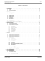
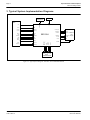
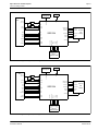
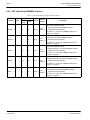
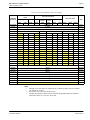
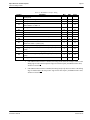
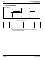
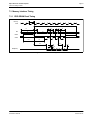
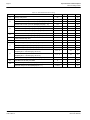
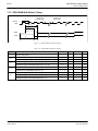
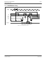
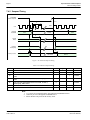
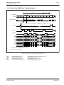
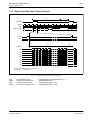
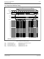
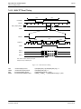
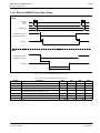
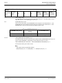
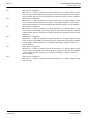
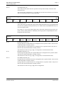
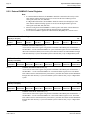
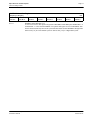
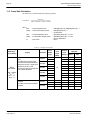
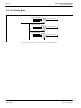
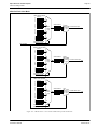
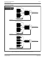
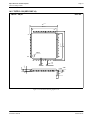
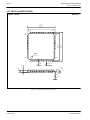
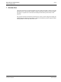
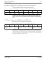
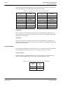
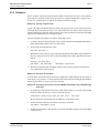
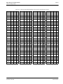
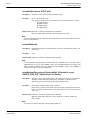
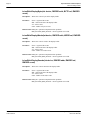
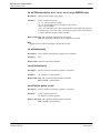
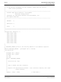
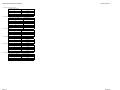
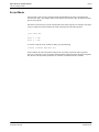
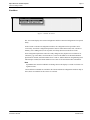
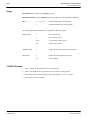
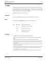
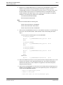
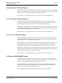
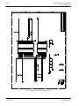
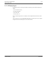
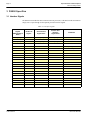
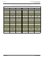
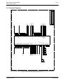
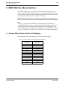
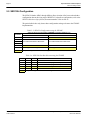
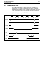
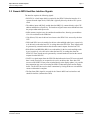
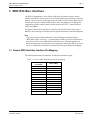
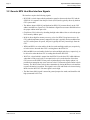
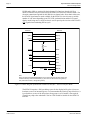
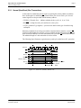
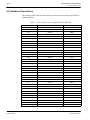
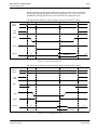
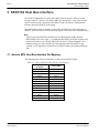
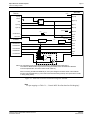
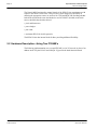
Page 76
Epson Research and Development
Vancouver Design Center
t1
Sync Timing
t2
FPFRAME
t3
t4
FPLINE
t5
MOD
Data Timing
FPLINE
t6
t8
t7
t9
t14
t10
t11
FPSHIFT
t12
UD[7:0]
LD[7:0]
t13
1
2
Figure 7-30: Single Color 16-Bit Panel A.C. Timing
Table 7-24: Single Color 16-Bit Panel A.C. Timing
Symbol
t1
1.
2.
3.
4.
5.
6.
Parameter
FPFRAME setup to FPLINE falling edge
Min
note 2
t2
FPFRAME hold from FPLINE falling edge
t3
FPLINE period
9
t4
FPLINE pulse width
t5
MOD delay from FPLINE falling edge
note 4
t6
FPSHIFT falling edge to FPLINE rising edge
note 5
t7
FPSHIFT falling edge to FPLINE falling edge
note 6
Typ
Max
Units
Ts (note 1)
note 3
9
Ts
t8
FPLINE falling edge to FPSHIFT falling edge
t14 + 3
Ts
t9
FPSHIFT period
5
Ts
t10
FPSHIFT pulse width low
2
Ts
t11
FPSHIFT pulse width high
2
Ts
t12
UD[7:0], LD[7:0] setup to FPSHIFT falling edge
2
Ts
t13
UD[7:0], LD[7:0] hold to FPSHIFT falling edge
2
Ts
t14
FPLINE falling edge to FPSHIFT rising edge
18
Ts
Ts
t1min
t3min
t5min
t6min
t7min
= pixel clock period = memory clock, [memory clock]/2, [memory clock]/3, [memory clock]/4 (see REG[19h] bits [1:0])
= t3min - 9Ts
= [((REG[04h] bits [6:0])+1)*8 + ((REG[05h] bits [4:0]) + 1)*8] Ts
= [((REG[04h] bits [6:0])+1)*8 - 1] Ts
= [(REG[05h] bits [4:0]) + 1)*8 - 25] Ts
= [((REG[05h] bits [4:0]) + 1)*8 - 16] Ts
SED1354
X19A-A-002-16
Hardware Functional Specification
Issue Date: 99/05/18