1
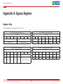
Appendix A: Bypass Register
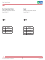
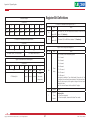
Register Bit Definitions
Slot Select Register
Offset 0xF9
7
6
5
4
3
2
1
PCB and CPLD Release Version Register (LSB): F1
0
R/W
R/W
R/W
R/W
R/W
R/W
R/W
R/W
Slot ID 7
Slot ID 6
Slot ID 5
Slot ID 4
Slot ID 3
Slot ID 2
Slot ID 1
Slot ID 0
Bit Field
3:0
7:4
PCB and CPLD Release Version Register (MSB)
Name
Value
CPLD
CPLD version LSB, for CPLD release version control, the MSB info at
version LSB
address ‘FD’, Read only
PCB
version LSB
PCB version LSB, the MSB info at address ‘FD’, Read only
Offset 0xFD
7
6
5
4
3
2
1
0
R
R
PCB version (MSB) / CPLD dot version
CPLD release version (MSB)
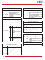
Bypass Timer Configuration Register: F2
Bit Field
Name
000 = 0 second, timer immediately expired
001 = 1 second
Bypass Time/Force Mode Control Register
010 = 2 second
Offset 0xFE
7
6
5
R
4
011 = 4 second
3
2
1
0
R/W
R/W
R/W
R/W
100 = 8 second
2:0
Timer/
CPLD identify bit
Unused
Unused
Unused
Timer
101 = 16 second
Value
110 = 32 second
111 = 64 second
force mode
This register is available in Timer Enable mode. Timer value of 1 to
7 is required to be written before expiration of the hardware timer.
When the timer expires, both segment relays which have been
enabled will close.
Note: The timer will recount while read/write F2 register.
independent
6:3
Unused
Segment
7
Timer
Expired
Copyright © 2013 NEXCOM International Co., Ltd. All Rights Reserved.
Value
51
Unused
Read only bit:
0 = Timer has not expired
1 = Timer has expired, de-assert while leave Timer mode
DNA 1150 User Manual