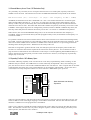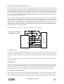
1
Issue B Second Edition 166 Designers Guide - Page 1 This guide contains basic information that is useful when doing your first 166 family design. There are many simple facts which if they are known at the outset can save a lot of time and money. Overall, it is intended as a complement to the user manuals by putting things into a practical context. Some of the material can be found in the 166 family databooks but most of it is simply the result of our practical experience and so is only to be found here. Topics covered are those that are not obvious or are often missed. Where the user manuals provide a satisfactory explanation, you will be referred to it rather than duplicating information here. This is by no means a complete reference work and you are directed to the excellent work by one of the architecture’s original designers Karl-Heinz Mattheis, available in the German language. Note: While every effort has been made to ensure the accuracy of the information contained within this guide, Hitex cannot be held responsible for the consequences of any errors contained therein. Any subjective or anecdotal information presented is not necessarily the official view of either Hitex Development Tools Ltd. or Siemens Plc.. Prepared By: Michael Beach John Barstow Karl Smith Additional Material From: Dave Greenhill Ulrich Beier Olaf Pfeiffer Peter Mariutti Second Editon, April 1999 Hitex produces the largest range of 166 family emulation and simulation tools available from any manufacturer. By using both standard part and bondout-based technology, Hitex can uniquely provide the optimal emulation method for all 166 variants, whatever the application. Besides supplying the development tools, Hitex is also pleased to help and advise new and prospective 166 users in all aspects of hardware and software design, as this guide demonstrates - we are at your service! Hitex Development Tools Ltd. University Of Warwick Science Park Sir William Lyons Road Coventry, CV4 7EZ Tel: 01203 692066 Fax: 01203 692066 Email: [email protected] Web: www.hitex.co.uk 166 Designers Guide - Page 2 166 Family Designer's Guide - Contents RISC Architectures For Embedded Applications ......................................................................................................... 6 Introduction ........................................................................................................................................................ 6 Behind The 166’s Near-RISC Core ................................................................................................................... 6 Conventional CISC Bottle-necks .................................................................................................................................. 6 The RISC Architecture For Embedded Control ............................................................................................................ 7 Basic Definitions: ............................................................................................................................................... 7 Bus Interface ...................................................................................................................................................... 8 RISC Interrupt Response .................................................................................................................................... 8 Registers And Multi-Tasking ........................................................................................................................................ 8 Coping With RISC Instruction Set (Apparent) Omissions .......................................................................................... 10 RISC And Real World Peripherals .............................................................................................................................. 11 1. Getting Started With The 166 ................................................................................................................................. 12 1.1 Basic Considerations .................................................................................................................................. 12 1.1.1 Family Overview ..................................................................................................................................... 12 1.1.2 Fundamental Design Factors ................................................................................................................... 12 1.2.1 Setting The CPU Hardware Configuration Options (166) ...................................................................... 12 1.2.2 Setting The CPU Hardware Configuration Options (167) ...................................................................... 12 1.3 Calculating The Pull-Down Resistor Values ......................................................................................................... 13 Pull Down Resistor Calculation ....................................................................................................................... 13 1.4 Pull-Up Resistor Calculations ............................................................................................................................... 13 Pull Up Resistor Calculation ............................................................................................................................ 14 1.4 Setting The Configuration Without Pulldown Resistors ....................................................................................... 14 1.5 Port 0 Configuration Functions ............................................................................................................................. 15 1.6 Reset Control ......................................................................................................................................................... 16 2. Clock Speeds And Sources ...................................................................................................................................... 17 2.1 166 Variants .......................................................................................................................................................... 17 2.2 165 And Basic 167 Variants .................................................................................................................................. 17 2.3 167SR & CR Variants ........................................................................................................................................... 17 2.4 Generating The Clock ........................................................................................................................................... 17 2.4.1 Designing Clock Circuits ........................................................................................................................ 17 2.4.2 Oscillator Modules .................................................................................................................................. 17 2.4.3 Designing Crystal Oscillator Circuits ..................................................................................................... 18 2.4.4 Crystal Oscillator Components Test Procedure ...................................................................................... 18 2.4.5 Typical Component Values ..................................................................................................................... 19 2.4.6 Laying Out Clock Circuits ...................................................................................................................... 20 2.4.7 Symptoms Of A Poor Clock ................................................................................................................... 20 3. Bus Modes ............................................................................................................................................................... 21 3.1 Flexible Bus Interface ........................................................................................................................................... 21 3.2 Setting The Bus Mode ........................................................................................................................................... 21 3.2.1 166 Variants ............................................................................................................................................ 21 3.2.2 C165/7 Derivatives ................................................................................................................................. 21 3.3 Setting The Overall Addressing Capabilities ........................................................................................................ 21 3.4 External Memory Access Times (167 Derivatives Only) ..................................................................................... 22 3.5 Expanding The Basic 166’s Memory Space ......................................................................................................... 22 4. Interfacing To External Devices ............................................................................................................................. 23 4.1 The Integral Chip Selects (167/5/4/3/1) ................................................................................................................ 23 4.2 Setting The Number Of Chip Selects .................................................................................................................... 24 4.3 READ/WRITE Chip Selects. ................................................................................................................................ 24 4.4 Replacing Address Lines With Chip Selects ......................................................................................................... 25 4.5 Generating Extra Chip Selects .............................................................................................................................. 26 4.6 Confirming How The Pull-Down Resistors Are Configured ................................................................................ 27 4.7 Generating Waitstates And Controlling Bus Cycle Timings ................................................................................ 27 5. Interfacing To External Memory Devices .............................................................................................................. 28 5.1 Using Byte-Wide Memory Devices In 16-bit 167 Systems .................................................................................. 29 166 Designers Guide - Page 3 5.2 Using The 166 With Byte-Wide Memories .......................................................................................................... 30 5.3 Using DRAM With The 166 Family ..................................................................................................................... 31 6. Single Chip 166 Family Considerations .................................................................................................................. 32 6.1 Single Chip Operation ........................................................................................................................................... 32 6.2 In-Circuit Reprogrammability Of FLASH EPROM ............................................................................................. 32 6.3 Total Security For Proprietary Software ............................................................................................................... 32 6.4 Keeping An External Bus ...................................................................................................................................... 32 6.5 Hitex’s In-Circuit FLASH Programming Utility Toolkit ...................................................................................... 32 6.5 Accommodating In-Circuit FLASH Programming ............................................................................................... 33 6.7 In-Circuit FLASH Programming Via CAN .......................................................................................................... 33 7. The Basic Memory Map .......................................................................................................................................... 34 7.1 On-Chip RAM Regions ......................................................................................................................................... 34 7.1.1 166 Variants ........................................................................................................................................... 34 7.1.2 167CR & 167SR, C165, Some 161 Variants ......................................................................................... 34 7.1.4 C167CS, C161CS ................................................................................................................................... 34 7.2 Planning The Memory Map .................................................................................................................................. 34 7.2.1 External ROM Applications .................................................................................................................... 34 7.2.2 Internal ROM Applications ..................................................................................................................... 35 7.3 A Typical 167 System Memory Map .................................................................................................................... 35 7.4 How CPU Throughput Is Related To The Bus Mode ........................................................................................... 36 7.5 Implications Of Bus Mode/Trading Port Pins For IO ........................................................................................... 36 8. System Programming Issues ................................................................................................................................... 37 8.1 Serial Port Baud Rates ........................................................................................................................................... 37 8.1.1 166 Variants ............................................................................................................................................ 37 Baudrates for 20 MHz ...................................................................................................................................... 37 Baudrates for 16 MHz ...................................................................................................................................... 37 8.1.2 Enhanced Baudrate Generator On 167 Variants ..................................................................................... 37 8.1.3 The Synchronous Port On The 167 ......................................................................................................... 37 8.2 Interrupt Performance ........................................................................................................................................... 37 8.2.1 Conventional Interrupt Servicing Factors ............................................................................................... 37 8.2.2 Event-Driven Data Transfers Via The PEC System ............................................................................... 38 PEC Usage Examples ....................................................................................................................................... 38 8.2.3 Extending The PEC Address Ranges And Sizes Above 64K ................................................................. 39 8.2.4 Software Interrupts .................................................................................................................................. 39 8.2.5 Hardware Traps ....................................................................................................................................... 39 8.2.6 Interrupt Vectors And Booting Up The 166 ........................................................................................... 39 8.2.7 Interrupt Structure ................................................................................................................................... 40 8.3 The Bootstrap Loader ............................................................................................................................................ 40 8.3.1 On-Chip Bootstrap Booted Systems ....................................................................................................... 40 8.3.2 Freeware Bootstrap Utilities For 167 ...................................................................................................... 41 8.4 166 Family Stacks ................................................................................................................................................. 41 8.5 Power Consumption .............................................................................................................................................. 42 8.6 Understanding The DPPs ...................................................................................................................................... 42 8.6.1 166 Derivatives ....................................................................................................................................... 42 8.6.2 167 Derivatives ....................................................................................................................................... 43 9. Allocating Pins/Port Pins In Your Application ....................................................................................................... 44 9.1 General Points About Parallel IO Ports ................................................................................................................. 44 9.2 Allocating Port Pins To Your Application ............................................................................................................ 44 9.3 Port 0 ..................................................................................................................................................................... 44 Port 0 Pin Allocations: ..................................................................................................................................... 44 9.4 Port 1 ..................................................................................................................................................................... 44 9.5 Port 2 ..................................................................................................................................................................... 45 9.5.1 The CAPCOM Unit ................................................................................................................................. 45 9.5.2 Time-Processor Unit Versus CAPCOM ................................................................................................. 45 9.5.3 32-bit Period Measurements ................................................................................................................... 45 9.5.4 Generating PWM With The 166 CAPCOM Unit ................................................................................... 46 9.5.5 Sinewave Synthesis Using The CAPCOM ............................................................................................. 46 166 Designers Guide - Page 4 9.5.6 Automotive Applications Of CAPCOM1 ............................................................................................... 46 9.5.7 Digital To Analog Conversion Using The CAPCOM Unit .................................................................... 47 9.5.8 Timebase Generation .............................................................................................................................. 47 9.5.9 Software UARTs ..................................................................................................................................... 48 9.6 Port 3 ..................................................................................................................................................................... 49 9.6.1 Using GPT1 ............................................................................................................................................. 49 9.6.2 Using GPT2 ............................................................................................................................................. 50 9.7 Port 4 ..................................................................................................................................................................... 50 9.7.1 Interfacing To CAN Networks ................................................................................................................ 50 9.8 Port 5 ..................................................................................................................................................................... 51 9.8.1 166 Analog To Digital Convertor ........................................................................................................... 51 9.8.2 167 Analog To Digital Convertor ........................................................................................................... 51 9.8.3 Over-Voltage Protected Analog Inputs ................................................................................................... 52 9.8.4 167/4-Specific Enhancements ................................................................................................................. 52 - wait-for-ADDAT-read mode ......................................................................................................................... 52 - channel injection ............................................................................................................................................ 52 - programmable sampling times ....................................................................................................................... 52 9.8.5 Matching The A/D Inputs To Signal Sources ......................................................................................... 53 9.8.6 165/3 ....................................................................................................................................................... 54 9.9 Port 6 (167) ............................................................................................................................................................ 54 9.10 Port 7 (167 Only) ................................................................................................................................................. 54 50ns PWM Module/High Resolution Digital To Analog Convertor ............................................................... 55 9.11 Port 8 (167 Only) ................................................................................................................................................. 55 9.12 Summary Of Port Pin Interrupt Capabilities ....................................................................................................... 55 9.12.1 Interrupts From Port Pins ...................................................................................................................... 55 9.12.2 166 Variants .......................................................................................................................................... 55 9.12.3 167 Variants .......................................................................................................................................... 55 9.13 Typical 166 Family Applications ........................................................................................................................ 56 9.13.1 Automotive Applications ...................................................................................................................... 56 9.13.2 Industrial Control Applications ............................................................................................................. 56 9.13.3 Telecommuncations Applications ......................................................................................................... 57 9.13.4 Transport Applications .......................................................................................................................... 57 9.13.5 Consumer Applications ......................................................................................................................... 57 9.13.6 Instrumentation Applications ................................................................................................................ 57 10. 166 Compatibility With Other Architectures ........................................................................................................ 58 11. Mounting 166 Family Devices .............................................................................................................................. 59 11.1 Package Types ..................................................................................................................................................... 59 11.2 Connecting Emulators To 166 Family Devices .................................................................................................. 60 11.2.1 Socketed Devices .................................................................................................................................. 60 11.2.2 The “PressON” Emulation Connector .................................................................................................. 60 11.3 166 Family PCBs ................................................................................................................................................. 60 11.4 CAD Symbols ...................................................................................................................................................... 60 12. Direct PCB Emulation Interfaces For 166 Designs .............................................................................................. 61 12.1 The Problem ............................................................................................................................................. 61 12.2 The ROMless Solution - ICEconnect166................................................................................................. 61 12.3 The ROM/ROMless Solution - QuadConnect ......................................................................................... 61 13. Getting New Boards Going ................................................................................................................................... 62 13.1 External Bus Design Pitfalls ................................................................................................................................ 62 13.2 Single Chip Designs ............................................................................................................................................ 64 13.3 Testing The System ............................................................................................................................................. 64 14. Conclusion ............................................................................................................................................................. 65 15. Acknowledgements ............................................................................................................................................... 65 16. Feedback ................................................................................................................................................................ 65 17. Contact Addresses ................................................................................................................................................. 65 Appendix 1 - Siemens C166 Family Part Numbers .................................................................................................... 66 166 Designers Guide - Page 5 RISC Architectures For Embedded Applications Introduction The 166 CPU core makes extensive use of Reduced Instruction Set Computer (RISC) concepts to acheive its blend of very high performance at modest cost. To understand why RISC techniques are especially suited to high-speed real time embedded systems, it might be useful to examine in detail how they grew out of the traditional Complex Instruction Set Computers (CISC) that reached their peak in the late 1980’s to early 1990’s. Behind The 166s Near-RISC Core The reasons behind the abandonment of traditional Complex Instruction Set Computers (CISC) has been the quest for ever greater throughput. The demands of workstations involved in CAD tasks and latterly advanced video games, have been the real driving force behind this. Traditionally, microprocessors have been designed with assembler instruction sets that have been geared towards making the assembler programmer’s life easier through the extensive use of microcode to produce ever more powerful instructions`. By providing single assembler instructions that perform, for instance, three operand multiplication, the assembler programmer (and HLL compiler writer) has been relieved of the job of achieving the same result with simpler instructions. The need for the CPU to be able to recognise and act on (decode) many hundreds of different instructions, requires complex silicon and many clock cycles. The greater the silicon area, the greater the cost of the device and power consumed. With physical limitations acting to restrict achievable clock speeds on silicon devices, the number of cycles per instruction is obviously very significant in gaining higher performance.. RISCs tend to shift the burden of programming from the microcoder to the assembler programmers and compiler writers. Work both within academia and commercial manufacturers has proved that a suitably programmed RISC machine can achieve a far higher throughput than a CISC for a given clock speed. Strangley, the embedded world has been slow to question the suitability of the CISC-based microcontroller. Whilst at the very top end, devices such as the i80960 have enjoyed some success, for more commonplace embedded tasks, RISC is almost unknown. With the increasing complexity of modern control algorithms, the need for greater processing power is set to become an issue in anything but the simplest applications. In addition, here more than in the workstation world, the worst-case response time to non-deterministic events is crucial, an area where CISCs are especially poor. Many current high-end microcontrollers are based on existing CISC architectures such as the 8086, 68000 etc., which in common with 8-bit devices such as the 8051, have an internal structure that dates back up to 19 years. With the silicon vendor’s need to give existing users an upgrade path, apparently new designs are often based closely on the existing architecture/instruction set, so protecting the user’s investment in expensive assembler-code. Like workstations, microcontrollers are tending to be programmed in a high level language (HLL) to reduce coding times and enhance maintainability. Inevitably, even with the best compilers, some loss of performance is encountered, emphasising again the need for improved CPU performance. In addition to straightforward data processing, microcontrollers must also handle real-world peripherals such as A/D converters, PWM’s, timers, Ports, PLL’s etc., all of which require real time processing. Conventional CISC Bottle-necks 1. Long And Unpredictable Interrupt Latencies Complicated “labour-saving” instructions must hold CPU’s entire attention during execution, thus preventing realworld generated interrupts from being serviced. Unpredictable latency times result which can cause serious problems in hard real-time systems. One approach to overcoming the CISC’s poor real-time response has been to bolt a secondary “time processor” onto the core to try and off-load the time-critical portions. However, this results in an awkward design and the need to use a very terse microcode to program it, in addition to the more usual C and assembler for the CISC core itself. 166 Designers Guide - Page 6 2. Vast Instruction Sets Give Slow Decoding Loaded instruction must be recognised from potentially many hundreds or even thousands of possibilities. Decoding is thus complicated and lengthy. 3. Frequent Accesses To Slow Memory Devices Data is typically fetched from off-chip memory and placed in accumlator-type registers. Mathematical or logical operations are performed and then result written back to memory. Value is likely to be required again in course of procedure, thus requiring further movements to and from off-chip memory. 4. Slow Procedure Calling When calling subroutines with parameters (essential in good HLL programming), parameters must be individually pushed on to stack. They must then be moved through accumulator register(s) for processing before being returned via stack to caller. 5. Strictly One Job At A time Each peripheral device or interrupt source must have dedicated service routine which at the least will require the PSW, PC to be stacked and restored and data removed from or fed to peripheral device. 6. Software Has To Be Structured To Suit Architecture. Embedded systems frequently contain many separate real time tasks which together form a complete system. Conventional CPU’s make switching between tasks slow. Often, many registers have to be stacked to free them up for the incoming task. This problem is aggravated by the use of HLL compilers which tend to use a large number of local variables in library functions which must be preserved. 7. Redundant Instructions And Addressing Modes With the move to HLLs, compilers are tending to dictate what instructions should be provided in silicon. In practice, compilers tend to only make use of a small number of addressing modes. This results in a large number of unused addressing modes which serve only to complicate the opcode decoding process. 8. Inconsistent Instruction Sets Instruction sets that have evolved tend to be difficult to use due to large number of different basic types and the inconsistent addressing modes allowed. 9. Bus Not Fully Utilised Whilst complex instructions are being executed, bus is idle. The RISC Architecture For Embedded Control To show how RISC design is used to improve microcontroller throughput, the 166 is used as an example. Basic Definitions: 1 state time = 2 * 1/oscillator frequency - fundamental unit of time recognised within processor system. 1 machine cycle = 2 * state time - minimum time required to perform the simplest meaningful task within cpu. 166 Designers Guide - Page 7 The unit of state times is used when making comparisons between RISCs and CISCs as this removes any dependency on clock frequency. - All state time counts are given in single chip operation mode for both 80C196 and 166. Bus Interface To maximise the rate at which instructions are executed, RISC CPU’s are very heavily pipelined. Here, on any given machine cycle, up to 4 instructions may be processed by overlapping the various steps thus: FETCH: DECODE: EXECUTE: WRITE-BACK: - get opcode from program store - identify opcode from a small list and fetch operands - perform operation denoted by opcode - result returned to specified location Thus although the instruction takes four machine cycles, it is apparently executed in just one (2 state times). Pipelining has considerable benefits for speeding sequential code execution as the bus is guaranteed to be fully occupied. RISC Interrupt Response In the 166, branches to interrupts make use of the injected instruction technique and so vectoring to a service routine is achieved in only 4 machine cycles (400ns). The effect of complex but necessary instructions such as MUL and DIV (5 and 10 cycles respectively) stretch this but it is interesting to note that the 80C166 does provide these as interruptable instructions. Very fast interrupt service is crucial in high-end applications such as engine management systems, servo drives and radar systems where real-world timings are is used in DSP-style calculations. As these normally form part of a larger closed control loop, erratic latency times manifest themselves as an undesirable jitter in the controlled variable. Registers And Multi-Tasking Traditional microcontrollers have one or more special registers which can be used for mathematical, logical or Boolean operations. In the 8051, there is a single “accumulator” with 8 other registers which may be used for handling local variables or intermediate results in complex calculations. These additional registers are also used to access memory locations via indirect and/or indexed addressing. As pointed out in section 3 and 4 above, conventional CPU’s spend much time moving data from slow memory areas into active registers. The RISC offers a very large number of general purpose registers which may be used for locals, parameters and intermediates. The 166 provides 16 word-wide general purpose registers (GPRs), each of which is effectively an accumulator, indirect pointer and index. With such a large number of GPR’s available, it becomes realistic to keep all locals and intermediates within the CPU throughout quite large procedures. This can yield a great increase in speed. Further significant benefits are derived from the RISC technique of register windowing. As has been said, up to 16 registers are available for use by the program. However, by making the active register bank movable within a larger on-chip RAM, the job of real time multi-tasking is considerably eased. Central to this is the concept of a “Context Pointer” (CP), which defines the current absolute base address of the active bank. Thus a reference to “R0” means the register at the address indicated by the CP. Thereafter, the 16 registers originating from CP are accessed by a fast 4-bit offset. The best example of how the CP is exploited is perhaps a background task and a real-time interrupt co-existing. When the interrupt occurs, rather than pushing all GPR’s onto the stack, the CP of the current register bank is stacked and simply switched to a new value, determined at link time, to yield a fresh register bank. This results in a complete context switch in just one machine cycle but does rule out the use of recursion. A hybrid method, which permits re-entrancy, uses the stack pointer to calculate the new CP dynamically. 166 Designers Guide - Page 8 Here, on entering the interrupt, the number of registers now required is subtracted from the current SP and the result placed in CP, with the old CP stacked. Thus the new register bank is located at the top of the old stack, with the old CP and then the new stack following on immediately afterwards. On exiting the interrupt routine, the original registerbank is restored by POPping the old CP from the stack. The SP is reinstated by adding the size of the new register bank onto the current SP. A further RISC refinement is register window overlapping whereby when a new procedure is called, part of the new register bank defined by CP’ is coincident with the original at CP: CP’ CP R7 R6 R5 R4 R3 R2 R1 R0 R3' R2' R1' R0' ; ; ; ; ; ; ; ; ; ; Register for subroutine’s locals Register for subroutine’s locals Common register, R7 == R1' Common register, R6 == R0' Register for caller’s locals and Register for caller’s locals and Register for caller’s locals and Register for caller’s locals and Register for caller’s locals and Register for caller’s locals and and intermediates and intermediates intermediates intermediates intermediates intermediates intermediates intermediates MODULE 1 ; *** Assignment Of GPRs To Local Variables - Caller *** x_var LIT y_var LIT ‘R0’ ‘R1’ ; Local variable ; Local variable parm1 LIT parm2 LIT ‘R6’ ‘R7’ ; Passed parameter 1 ; Passed parameter 2 result LIT ‘R6’ ; Value returned from sub routine ^^^^^^^^^^^^^^^^^^^^^^^^^^^^^^^^^^^^^^^^^^^^^^^^^^^^^^^^^^^^^ MODULE 2 ; *** Assignment Of GPRs To Local Variables - Sub Routine *** a_var LIT b_var LIT ‘R2’ ‘R3’ input1 input2 ret1 LIT LIT LIT ‘R0’ ; Local variable ; Local variable ‘R0’ ‘R1’ ; Received parameter 1 ; Received parameter 2 ; Final result returned in R0 Fig. A - Giving GPR’s Meaningful Names By using some forethought, the programmer should arrange for any value to be passed to the sub routine to be located in the common area, so that all the normal loading and unloading of parameters is avoided. This technique can be used in either absolute or SP-relative registerbank modes. To get the best from a RISC’s registers, the location of data needs close consideration: although highly orthogonal, the limited number of addressing modes provided for MUL and DIV for example, can appear somewhat restrictive. Fortunately though, most operands involved will already be in registers, so eliminating the need for many addressing techniques. As might be expected, the instructions with the widest range of addressing modes are the simple data moves - the fact that RISC’s are the result of very careful analysis of the requirements for fast execution becomes obvious after a short acquaintance! 166 Designers Guide - Page 9 Coping With RISC Instruction Set (Apparent) Omissions With largely single machine cycle execution, some conventional “fast” instructions such as CLEAR, INC and DEC become redundant. Therefore, to keep the total number of instructions to a minimum, RISC’s simply omit them. Examples are given below: Instruction 80C196 States 80C166 States ------------------------------------------------------------Clear Word CLR 4 AND Rn,#0 2 Decrement Word DEC 4 SUB Rn,#01 2 Increment Word INC 4 ADD Rn,#01 2 - all direct addressing mode Three-operand instructions are also commonplace in CISCs but not present in RISCs. Although additional instructions are required, the overall number of states is still less than the three operand CISC equivalent, plus the shorter RISC instructions allow greater opportunity for interrupt servicing. The following example illustrates this: Perform: z = x + y 80C196 (CISC) z,x and y are directly addressed memory locations x y z DW DW DW 1 1 1 ADD z,x,y ; 5 states - no interrupt possible 166 (RISC) z,x and y are memory locations, Rw is a GPR x y z DW DW DW 1 1 1 MOV Rw,x ADD Rw,y MOV z,Rw ; ; ; ; ; ; ; 2 states * Interruptable here 2 states * Interruptable here 2 states ———— 6 states One extra state required when using RISC approach. However, if the variables are assigned recognising that this is a RISC: x and y are memory locations, z is a GPR x y DW DW 1 1 z LIT ‘R0’ ; z is assigned to GPR R0 via a LITeral definition MOV z,x ADD z,y ; ; ; ; ; 2 states * Interruptable here 2 states ———— 4 states - 1 state saved over CISC. The above was chosen as a worst case RISC, best case CISC example. 166 Designers Guide - Page 10 For a normal 2 operand ADD, the RISC uses two states compared to the CISC’s 4, a 50% improvement. - Assigning all variables to GPR’s would probably make sense in the context of a real program. - This trivial example shows how familiarity with RISCs programming techniques improves performance. RISC And Real World Peripherals Within the workstation RISC, superscalar operation allows parallel execution of instructions, made possible by having discrete addition, multiplication, shift and other dedicated units, each with their own pipelines. No RISC microcontroller (yet) offers quite this but something similar is possible to service on-chip peripherals such as an A/D converter. A common situation occurs in conventional microcontrollers whereby some regular event requires attention from the CPU to load or unload data. Typically, an A/D converter will cyclically read a number of channels, causing an interrupt when completed or simply waiting for the CPU to poll its status. The net result is the valuable CPU time is spent doing what even for a microcontroller is a simple, repetitive task. The RISC 166 allows the interrupt service routine to be serviced and completed in a single machine cycle. In the case of a periodic A/D conversion, on each read the result is stored in a table where they may be retrieved by the CPU when convenient. This mechanism requires the CPU to perform only a single MOV [table_addr+],ADDAT after each conversion. At the end of the table, an additional cycle is required to reset the table pointer. Any real-world generated data can be handled in this way, leaving the CPU free for data processing rather than simple data collection. RISC Benefits In Embedded Applications 1. Near-DSP throughput For example, the 166 can acheive 10 million instructions per second (10MIPS) at 20MHz clock (100ns machine cycle time). At 25MHz this rises to 12.5MIPS with an 80ns cycle time. This is a result of pipelining and the ability to contain the active data for entire procedures within the CPU registers. 2. Simpler Assembler Coding Although instruction set is less diverse, the consistency of addressing modes makes assembler coding easier. 3. Very Fast Response To Non-Deterministic Events By eliminating instructions that take many cycles, interrupt response is improved. Smaller instructions effectively yield higher “sampling rate” for real world events. 4. Single Machine Cycle Context Switching By careful use of multiple register banks controlled by a base pointer, context switching in a multitasking system can be performed in just one 100ns cycle (80ns at 25MHz). In addition, parameter passing overhead to subroutines is eliminated by use of overlapping register windows, so that parameters lie in the common area. 166 Designers Guide - Page 11 1. Getting Started With The 166 1.1 Basic Considerations 1.1.1 Family Overview The 166 family now includes the C161, 163, 165 and 167, which amounts to around 20 different microcontrollers when all the variants are considered. It is an original core design and so is not directly related to any previous architecture. The first family member was the 166, available in masked ROM, FLASH EPROM and ROMless versions. The second member was the 167 which had an expanded addressing capability, integral chip selects plus many more peripherals and introduced some new assembler instructions. In fact, all the subsequent versions have been based on the 167 core. This includes the C161, C164, 163 and 165. In this guide, the original 166 cored-versions will be referred to as the “166” while the 167 and its derivatives that share the enhanced core will be known as the “167”. Unless specific peripherals are being referred to, what is appropriate to the 167 will apply equally to its derivatives. 1.1.2 Fundamental Design Factors When starting out on a 166 family design, there are a number of basic things you must decide. Wrong decisions here can have expensive consequences later in the project. There are a good many features of the architecture which can be a bit puzzling to those used to conventional devices. What follows is a simple guide to what you really need to know to get best from this ingenious and powerful microcontroller family! * * * * * * * * * * * * What clock speed is required to acheive the necessary CPU processing power? What sort of clock source is suitable? What sort of reset circuit should be used? What CPU sockets are available? How is the on-chip ROM or FLASH EPROM to be programmed? How is external FLASH EPROM to be programmed? Is a full 16 bit bus necessary or will an 8-bit bus be sufficient? Will there be some external peripheral chips that will require different bus modes? How much IO is required to implement the application? Should WRH/WRL be used? Should the chip selects be used? Which peripheral pins are best allocated to the various different signal processing or generation functions in the application? And others... 1.2.1 Setting The CPU Hardware Configuration Options (166) While in reset, the 166 reads the EBC0, EBC1 and /BUSACT pins to determine which bus mode is to be used. This information is then written into the appropriate fields in the SYSCON special function register. 1.2.2 Setting The CPU Hardware Configuration Options (167) In common with many modern microcontrollers, between the /RESIN pin going high and the rising edge of the first ALE pulse, the 167 reads the bit pattern on Port 0 to determine the following fundamental settings: * * * * * * What the default bus mode is How many pins on port 6 should be used as chip selects How many address lines should be used Whether the on-circuit emulation mode is be entered Whether the WRITEHIGH/WRITELOW mode required Whether the BOOTSTRAP mode is to be activated The pattern is placed onto the port by the user attaching pull-down resistors to the appropriate P0 pins. For example, to set 16 bit non-multiplexed bus mode, a pull-down resistor is added to P0.7, while P0.6 floats high. The values of the pull-down resistors should be calculated with reference to the overall loading on Port 0, from external memory devices etc., using the formulae given in section 1.3. The value required for a typical 1 EPROM + 1 RAM 166 Designers Guide - Page 12 system is 8K0, this representing the stated maximum value and covers 90% of all designs seen to date. In extreme cases, as little as 1K8 can be used but this is exceptional as the leakage currents from modern memory devices are extremely small. Overall, the user is simply advised to check the situation in the design and not to just to blindly accept the usual 8K0 value! Note: The databooks frequently refer to port 0 either as a 16-bit port or as two 8-bit ports, made up of P0L (LOW) and P0H (HIGH). Thus P0.15 is bit-16 on port 0 which is also P0H.7. By the same convention, P0.7 is also known as P0L.7. 1.3 Calculating The Pull-Down Resistor Values Finding the value of the pull-down resistors for your design is fairly straightforward. You will need to know the leakage current from the devices such as RAMs, ROMs etc that are attached to the bus. input leakage current input current Vcc RESET IP0L >= 100uA I SYSL Pull-Down Resistor Current Flow Port 0 I PD R PD V IN = V ILMAX System. 167 VILMAX = Highest voltage that will be accepted as a ‘0’ ISYSL = Leakage current from RAMs, ROMs etc. IP0L = Current flow from 167’s Port 0 when pin is at VILMAX RPD = Pull down resistor on Port 0 From 167 Databook: VILMAX = (0.2 x Vcc) - 0.1V => 0.8V <= VILMAX =< 1.0V Vcc = 5V +/-10% => 4.5V =< Vcc =< 5.5V Pull Down Resistor Calculation RPD < VILMAX = VILMAX IPD IP0L + ISYSL Example Without System Leakage Current, ISYSL: RPD < VILMAX = 0.8V IP0L 100uA = 8K0 Thus the maximum recommended value is RPD = 8K0. In practice, 8K2 is almost always used. 1.4 Pull-Up Resistor Calculations In some designs, the loading on the bus can be such that there is a net flow of current into the external devices to ground, i.e. the bus sinks current. In extreme cases, this can cause the port 0 pattern read by the 167 to be incorrect. It must be stressed that this very rare but can easily be compensated for by using a high-value pull-up resistor. Such measures are only required if the current sunk into the external device ISYSH, is greater or equal to 10uA. Before finalising any design the condition should be checked for and a pull-up resistor added if necessary. The procedure for calculating the pull-up resistor is as follows: 166 Designers Guide - Page 13 Vcc input leakage current input current Vcc R PU I PU RESET IP0H <= 10uA Pull-Up Resistors On Port 0 I SYSH Port 0 V IN = V IHMIN System. 167 VIHMIN = Lowest voltage on pin that will be accepted as a ‘1’ ISYSH = Current sunk into bus devices etc. IP0H = Current that can be drawn from 167’s Port 0 at VIHMIN RPU = Pull up resistor on P0 From 167 Databook: VIHMIN = 0.2 x Vcc + 0.9v - 0,1V => 1.8V <= VIHMIN =< 2.0V Vcc = 5V +/-10% => 4.5V =< VCC =< 5.5V Pull Up Resistor Calculation RPu < VPU IPD = VCCMIN - VIHMIN ISYSH - IP0H Example: ISYSL = 50uA RPU < 4.5v - 1.8v 50uA - 10uA = 67.6K 1.4 Setting The Configuration Without Pulldown Resistors It is possible to use a simple analog-type switch to set the pattern on port 0 in external bus designs. Here, the links to ground are only applied to the port 0 pins when the /RESIN signal is low, i.e. the 166 is in reset. The D-type latch powers up with the Q output low so that the link pattern is applied to port 0. When the RESET signal goes high to release the CPU, the switch is kept active until the first rising edge of ALE at the start of the first bus cycle. At this point the CLK signal forces the latch to set Q high so that the link pattern is removed and the bus operates normally. Waiting until the first ALE is essential - controlling the switches from /RESIN alone could result in the CPU reading the pattern after it has been removed! Active Port 0 Configuration Scheme 167 Quick Switch P0L.0 Bootstrap Mode Bus Mode P0L.7 /RESIN /EN Vcc S D ALE Links Q 74x74 GND /CLR CLK /Q RESET CIRCUIT 166 Designers Guide - Page 14 1.5 Port 0 Configuration Functions This diagram gives the individual configuration functions of the port 0 pins when CPU is between the end of reset and the rising edge of the first ALE: P0.15 P0.7 P0.0 P0H.7 P0L.7 P0L.0 Clock Generator 10 9 SASEL CSSEL Port 4 Logic Port 6 Logic SYSCON 8 7 6 BUSTYP 5 4 R 3 2 R 1 R 0 EMU CLKCFG 11 ADP 12 BSL 13 WRC 14 RP0H 15 BUSCON0 167 Special Function Registers EMU - Emulation mode allows the XBUS peripherals to be accessed by an external 167 core. This is used on the DPROBE167 bondout in-circuit emulator to allow the C167E-BA emulation chip to access the CAN peripheral and XRAM on the slave 167 processor on the EP167-Y. DO NOT FIT A PULL DOWN RESISTOR ON THIS PIN! ADP - On-circuit emulation mode puts all the 167 pins into a high-impedance tristate condition so that an emulator’s clip-over adaptor can be attached to a soldered-in device. Note that if the clock source is a crystal, pin XTAL2 must be disconnected from the processor so that the emulator’s CPU can pick up the clock. DO NOT FIT A PULL DOWN RESISTOR ON THIS PIN! R - Reserved, do not use! BSL - Enables the bootstrap loader mode for on- and off-chip FLASH-programming etc.. See section 9.3. BUSTYP - The external bus type can be set as shown below. These two pins form the BUSTYP field in the BUSCON0 special function register, where it can be modified by software. P0.7 0 0 1 1 P0.6 0 1 0 1 External Bus Mode 8-bit non-multiplexed 8-bit multiplexed 16-bit non-multiplexed 16-bit multiplexed (DEFAULT - no pull-down) WRC - Cause the /WR pin to become /WRH (write high) and /BHE to become /WRL (write low) to make the use of 8-bit RAMs in a 16-bit system easier. See section 5.1. CSSEL - The number of chip selects that are to be enabled on port 6 - see section 4.1. CSSEL 1 1 1 0 0 1 0 0 Chip Select Lines On Port 6 Five: /CS4, /CS3, /CS2, /CS1, /CS0 (DEFAULT - no pull-down) None: Two: /CS1, /CS0 Three: /CS2, /CS1, /CS0 166 Designers Guide - Page 15 SALSEL - Number of “segment address” lines, i.e. how many additional address lines above A15 will be enabled. SALSEL 1 1 1 0 0 1 0 0 CLKCFG 1 1 1 1 0 Segment Address Lines On Port 4 Two: A16, A17 (DEFAULT - no pull-down) Eight: A16 - A23 None: (“NONSEGMENTED” or “TINY Model” - very rare!) Four: A16 - A19 - Programming for processor clock input, with optional phase lock loop (PLL) clock multiplier. CLKCFG 1 1 0 0 X . 1 0 1 0 X Clock Generator Frequency Multiplier Control x4 (DEFAULT - no pull-down) x3 x2 x5 Direct Drive 1.6 Reset Control The 166 family has two reset pins, /RESIN and /RESOUT. The former is a conventional active-low reset input while /RESOUT is an output pin which stays low until the CPU executes the EINIT (end-of-initialisation) instruction. /RESOUT is thus a means of keeping peripheral devices in a reset state until the CPU is fully initialised. The /RESIN input must be kept low for the duration of the startup phase of the clock oscillator or crystal - the latter requires up to 50ms. Once stable, any low level on /RESIN of more than two state times (100ns @ 20MHz) will reset the CPU. Low times of less than this must be avoided. The pin has an internal pull-up resistance of between 50k and 150k, so the simplest reset circuit is just a capacitor to ground. The value must be chosen to give a time constant of at least equal to the clock stabilisation time. 22uF is a common choice. Vcc 50K - 150K Simple Reset Scheme /RESIN RESET 22uF 166 GND However, such a simple arrangement is not suitable for use in those situations where the power supply could suffer from instability or brown-outs. In most commercial products, the use of a proper microprocessor power supply and RESET manager such as the MAX691 is highly recommended. This low-cost device will hold the CPU in RESET if the power supply is less than 4.5v. 166 Designers Guide - Page 16 2. Clock Speeds And Sources 2.1 166 Variants The original 166 has a divide by two prescaler so that a 40MHz crystal or oscillator is required to yield the maximum possible 20MHz CPU clock. The basic unit of time in the 166 core is a single state time, corresponding to 50ns at 20MHz. Most 166 instructions execute in two state times, i.e. 100ns. The ‘W’-suffixed 166 parts have no divide-by-two and thus can use a 20MHz clock source directly. These parts must be used with a crystal as they demand a 50% duty cycle clock, which cannot be guaranteed with an oscillator module. If an oscillator module is used, it must have a rise and fall time of <5ns. Such devices are readily available at a few pounds each. 2.2 165 And Basic 167 Variants From stepping level BA, the 165 versions can run with either 40 or 20MHz clock sources. The presence of a pulldown resistor on P0.15 will cause the CPU to expect a 1:1 clock rather than a 2:1. 2.3 167SR & CR Variants The 167CR and 167SR are all of the ‘W’ type in that they can use a 20MHz crystal. They can also use a 5MHz crystal and use the on-chip phase-lock loop (PLL) to perform a programmable frequency multiplication up to the usual 20MHz or newer 25MHz. The PLL is disabled by a pull-down resistor on Port P0.15. From C167CR BA step onwards, the PLL can provide frequency multipliers of x1, x2, x3, x4 and x5, so that in the latter case, a 5MHz crystal will yield a 25MHz clock. The exact multiplier is set via pull-down resistors on P0.14 & P0.13 (P0H.6 & 5). The default multiplier is x4, corresponding to no pull-down resistors. Test Configuration 167xR 167xR Fundamental Mode A0-A18..A23 A0-A18..A23 XTAL2 XTAL2 XTAL1 XTAL1 RX RX 5MHz CX1 5MHz CX2 P06,7 P06,7 P0.15 P0.15 GND (PLL Enable) Rq GND (PLL Enable) GND Iq From Current Probe 2.4 Generating The Clock 2.4.1 Designing Clock Circuits There are two basic choices of clock source, the crystal or a self-contained oscillator module. The design of a traditional clock circuit is not a trivial task and requires some care to get reliable start-up when production tolerances and component ageing is taken into account. The 166 is family is no more demanding in this area than any other microcontroller so the hints given in the following section should be considered for any clock circuit design. 2.4.2 Oscillator Modules Using an oscillator module is very simple as the operating point calculations will have been taken care of by the manufacturer. The EMC emissions are also less as the metal case is always grounded and there will be a shorter signal path. The only critical factor is that the rise and fall time should be less than 5ns. There is a small price 166 Designers Guide - Page 17 premium over the conventional crystal-plus-capacitors approach but this is not great. Indeed, it is only if the microcontroller is going to be used in a 25k+ per annum quantity that the extra cost of a module is going to become significant. The oscillator output should be connected to the 166’s XTAL1 pin. 2.4.3 Designing Crystal Oscillator Circuits The traditional clock circuit usually comprises a parallel resonant fundamental crystal plus two capacitors and a resistor to limit the current through the resonant device. The selection of the series resistor value Rx must be made so that the oscillator is guaranteed to start within 0.1ms to 5ms, even after mass production tolerances and ageing effects are taken into account. It must also be chosen to keep the power drive level of the crystal between typically 50uW to 800uW, although the device’s datasheet should be consulted. The process of defining RX and the “load capacitors”, CX1 and CX2, is aimed at making sure that there is sufficient current flowing through crystal to drive the on-chip inverter that produces the oscillation. The crystal has a characteristic resistance known as the “equivalent series resistance” or “load resonant resistance”, which is a combination of its typical resistance (R1typ) and residual capacitance (C0typ), as stated by the manufacturer, plus reactive effects due to the oscillation and the load capacitors CX1 and CX2. This equivalent resistance is given by: RL = R1typ x (1 + (C0typ/CL)2) Where: CL = (CX1 x CX2)/(CX1 + CX2) + CS (CS = the stray capacitance of clock circuit) During this Rx definition phase, a small value resistor, Rq, should be inserted in series with the crystal. The temporary resistor, Rq, must be increased until the oscillator does not start automatically when the 166 is powered up for different values of load capacitor. This value will be Rqmax. For ease of adjustment, an RF potentiometer can be used but you must bear in mind that this is RF engineering and the value of Rq so arrived at must be verified by replacing the potentiometer with an equivalent SMD or RF resistor and repeating the test. The ratio of Rqmax to the equivalent series resistance is the “Safety Factor” and is a measure of how much spare capacity there is in the circuit to overcome tolerance and ageing effects: Safety Factor (SF) = Rqmax/RL A current probe should be used to measure the peak-to-peak current (Ipp), converted to drive power with: Pw = (Ipp x Ipp x RL)/8 The resulting relationships between safety factor and power drive versus load capacitor value should be plotted on graph paper. From both curves, a value of load capacitors that gives the best combination of safety factor and power consumption can be chosen. 2.4.4 Crystal Oscillator Components Test Procedure 1. Select a value for Rx 2. Fit load capacitors, CX1 and CX2 of the value given in the table 3. Adjust Rq until oscillation will not self-start in less than 5ms when the 166 is powered-on. Record this resistance in a table, similar to than given below: Test Record For Rx = 680R CX1 = CX2 Ipp 0.0pF 0.002075 2.2pF 0.002300 4.7pF 0.002550 10pF 0.003100 22pF 0.004550 47pF 0.008000 Pw 25.27 26.09 27.48 32.17 51.59 122.50 Rqmax 150 500 750 600 250 60 4. Select the next value of load capacitors and repeat steps 2 to 4 Now pick another value for Rx and repeat the procedure. 166 Designers Guide - Page 18 After a number of Rx values have been tested in this way, the resulting curves should be examined for the resistor and load capacitor values that give the best safety factor at a power level of 50uW-800uW. Having selected the values, the resistor Rq should be removed and the current and start-up times rechecked. If an adequate safety factor cannot be achieved, particularly above 20MHz, it is possible to add a series 1-10M resistor to increase the feedback to the XTAL1 input pin. Otherwise, a third-overtone mode must be used. Unfortunately, the component selection process is more complex and when it is considered that an extra inductor and capacitor will be required to damp-out the fundamental frequency, it might prove more cost-effective to use an oscillator module! To simplify the selection process, Hitex can provide an EXCEL spreadsheet template that automates the conversion of test results and characteristic curve plotting, as illustrated below: Region Of Acceptable Safety Factor Region Of Acceptable Power Level Excel Spreadsheet For Component Evaluation The clock circuit will in fact produce two drive currents: until the RESOUT pin goes high, (after the EINIT instruction is executed), the current drive of the clock will be greater to ensure that the CPU is less likely to be upset during the potentially noisy initialisation phase. It also helps to overcome the initial high resistance of the crystal during the startup phase. Typical load capacitor values are 22pF with Rx around 1K. However, you should not rely on these and for any serious project, the selection procedure given earlier should be followed. 2.4.5 Typical Component Values The table gives typical values for a selection of commercially available crystals. These must not be used as they stand without testing - we deliberately have not given the brand names for this reason! It is recommended that you compare the characteristics C0typ, R1typ (in the shaded panels) and fundamental frequency of your device with the examples in the table and pick the one which is closest. Make up a clock circuit using the load capacitors CX1 and CX2 plus series resistor Rx and perform the check of safety factor and drive power given in the previous section. The chances are that the results will be within limits but it would be very embarassing if reliability problems occur in production and you have to admit that you never verified the component values in the clock circuit.... 166 Designers Guide - Page 19 CX2 (pF) CL (pF) C0typ (pF) R1typ (Ohm) R1max (Ohm) R1max (TK) (Ohm) Pw (uW) 12 15 13 7 10 50 60 420 300 2.11 32 0 12 15 11 5 15 50 60 520 390 3.07 24 180 15 22 12 5 15 50 60 510 390 3.24 20 390 8.2 39 10 4 20 60 80 375 560 3.57 18 390 12 39 14 4 20 60 80 335 540 4.08 16 390 12 47 13 4 20 60 80 353 580 4.24 12 390 15 47 13 4 30 70 90 312 1000 6.50 100 216 1200 8.14 Safety Factor (SF) CX1 (pF) 0 Rqmax (Ohm) Frequency (MHz) Rx2 (Ohm) 40 10 390 15 47 14 3 30 80 8 390 15 47 15 3 35 80 100 372 1800 12.50 6 390 15 47 14 3 35 80 140 100 2200 10.66 5 390 22 47 18 3 35 80 140 110 2700 14.17 4 390 22 47 16 4 20 80 150 46 Typical Crystal Characteristics And Component Values 3300 14.08 2.4.6 Laying Out Clock Circuits The layout of the clock circuit can be critical in determining both the RF emissions and susceptibility of a 166 design. As with any high frequency system, the loop areas must but kept as small as possible, meaning in practice that all components must be located as close as practicable to each other and the XTAL1/XTAL2 pins on the CPU. With metal-canned crystals, the case should be soldered to a grounded area on the top surface plus be connected to the main ground layer in a multi-layer board. This will also improve the mechanical stability of the part. 166 Decoupling capacitor on reverse of board CB Vss XTAL2 RX Vcc XTAL1 CX1 = Connections to ground layer CX2 Sample Oscillator Circuit Layout Crystal Inductive and capacitive coupling can be reduced by eliminating parallel runs of tracks either on the same layer or between layers. The grounding of the load capacitors should have a generous track width and be connected directly to the ground layer to avoid ground loops which are a major source of RF emissions. 2.4.7 Symptoms Of A Poor Clock It must be emphasised that the series resistor value must be chosen with care. An incorrect value is unlikely to result in a total CPU failure, or even erratic operation of the core, timers or A/D converter. However, the first 166 Designers Guide - Page 20 symptom of a poor choice is that an unexpectedly large number of bus errors on the CAN peripheral may be seen, or the ALE timing is erratic for no readily apparent reason. Such behaviour should never be ignored - try shorting the resistor out to see if the problem goes away.... Note: For more information on oscillator design, please refer to the application note by Peter Mariutti. 3. Bus Modes 3.1 Flexible Bus Interface The basic philosophy behind the 166 bus interface is simplicity; by providing 8- and 16-bit non-multiplexed modes, it is possible to dispense with an address latch and provide just a ROM and RAM to make a working 166 system. With the 167, the integral software-programmable chip selects can make most address decoder logic redundant. Thus, despite its 20 fold improvement in performance, a 166 digital design can be simpler than an 8031! One of the 166’s most useful features is its ability to support two different bus configurations in a single hardware design. Thus whilst the main code and data areas can be 16-bit non-multiplexed with zero waitstates for best speed, slow (and low cost) peripherals such as RTCs can be addressed with, for example, an 8-bit bus with 3 waitstates. This secondary bus mode is controlled by the BUSCON1 and ADDRESEL1 registers which set the mode and address range base address respectively. In the 167, a further 3 secondary bus regions can be defined, each with its own BUSCON and ADDRSEL registers plus an external chip select (/CS) pin for direct connection to peripheral devices’ chip enable inputs. These pins can remove the need for any external address decoding GALs etc.. It is essential when setting up the ADDRSEL and BUSCON registers to make sure that you configure the ADDRESELx before the corresponding BUSCONx. If you do not, the CPU will enable the ADDRSEL for an undefined bus configuration and a crash will ensue! Also note that while you may initialise these registers from C, any variables located in an region controlled by them will not be zeroed before main() as the corresponding chip select will not be active (low). It is therefore better to put your BUSCON and ADDRSEL set ups just after the SYSCON and BUSCON0 initialisations in the C compiler’s START167.A66 or CSTART.ASM. 3.2 Setting The Bus Mode 3.2.1 166 Variants This uses two dedicated pins (EBC0/1) to determine the bus mode coming out of reset. These two pins are effectively written into the BTYP field in the SYSCON register. This default bus mode can be overridden by the user writing into the BTYP field but this is not recommended. 3.2.2 C165/7 Derivatives When coming out of reset, the 167 reads the pattern of user-defined pull-down resistors on the P0.6 and P0.7 to set the default bus mode. In fact, the pull-down resistor pattern is placed into the BTYP field in the BUSCON0 register where it can be changed by software, although it definitely not recommended to do this on external ROM designs. The number of chip selects and the overall address range of the processor are also set via PORT0 pull-down resistors, covered in section 4.1. 3.3 Setting The Overall Addressing Capabilities The default memory space for the 167 is 256kb as port 0 provides 16 address lines and port 4 supplies A16 and A17, which act as two “segment address lines”, just as with the 166 variants. It is possible to enable four segment address on port 4 lines to give A0-A19, i.e. 1MB. Ultimately, all 8 segment address lines can be enabled to give A0-A23 and thus a 16MB addressing range. The number of segment address lines is determined by the presence of pull down resistors on P0.9 & P0.10. No resistors results in two segment address lines and a 256kb address space. Somewhat confusingly, the 167CR has the CAN TX and RX on the P4.5 (A21) and P4.6 (A22) pins, apparently limiting the memory space to 1MB. In fact this is not the case as the 5 chip selects can be used to expand the space back up to 5MB, as is demonstrated in section 4.4. 166 Designers Guide - Page 21 3.4 External Memory Access Times (167 Derivatives Only) As a potentially very fast CPU, the 167 can require fast memories to run at full speed, especially if the newer 25MHz versions are used. The minimum access times for EPROMs and RAMs is easily found via the formula: ROM Access Time (ns) = 2000/Fcpu - 30 (Fcpu = CPU frequency in MHz = 20MHz) At 20MHz, the minimum access time is 2000/20E6 -30 = 70ns. This assumes that there are no external signal delays through address decoders etc.. If the 167’s own chip selects are being used to enable memory devices directly via their /CE pins, the 20ns delay due to the internal address decoding logic must be subracted from the minimum access time of 70ns. This means that when used as address chip selects, the memory access time is 50ns at 20MHz. If the integral chip selects are configured (by software) instead as READ or WRITE chip selects, the 20ns chip select delay does not influence the memory access time - see section 4.3 “Read/Write Chip Selects” With common, low-cost FLASH EPROMs being 90ns, it can be seen that the maximum clock frequency is 16.67MHz. With a typical external memory decoder propagation delay of 5ns, the maximum clock frequency is a convenient 16MHz. It is possible to make the 166 insert waitstates itself to allow slower memories to be used but this should generally be avoided. Tests have shown that it is more efficient to reduce the clock speed rather than insert waitstates. In the usual case of either 16MHz with no waitstates or 20MHz with a waitstate, there is a 3% processing performance advantage from choosing the former. Waitstates are the enemy of the 167! If the PLL is being used to generate the CPU clock, the small jitter present in the frequency must be taken into account as it will tend to decrease the required access time for the memory devices. You are advised to refer to page 44 of the 167 data sheet for more information on this subject. If ALE lengthening, READ/WRITE delays or memory tristate times are being used, you must account for these also. However, in the majority of present-day designs, they are not used. 3.5 Expanding The Basic 166s Memory Space A18 A17 A16 Port 4 - A17 Port 4 - A16 A1 Port 2 - P2.15 Port 2 - P2.14 A0 166 A15 A18 A17 A17 A16 A1 A1 A0 27F040 27F040 1MB FLASH A17 The 256kb addressing capability of the 166 derivatives can be easily expanded using “bank-switching” so that 1MB can easily be reached - the 16MB of the 167 cannot realistically be duplicated! Here, some ordinary port pins, such as P2.14 and 2.15 can be used as additional address lines A18 and A19. The C compiler kits can be made to automatically drive these pins so that virtual addresses can be assigned to code and data. As far as the user is concerned, this is totally transparent and the 166 can be treated as a 1MB address space processor. Bank-Switched 166 Memory Expansion There are some side effects to this that must be taken into account: as 166 port pins are inputs after reset, the A18 and A19 “address” lines will be high, implying a virtual address of 0xC0000. The user must therefore make sure that there is a JMP vector to the program start at this address. There is only a software overhead due to bank-switching when code or data is accessed in other than the current bank. This amounts to around 1us, every time a change is required. Careful software design, particularly in the linker input file, will make this a rare condition. 166 Designers Guide - Page 22 4. Interfacing To External Devices 4.1 The Integral Chip Selects (167/5/4/3/1) The 167 derivatives have IO pins on port 6 that can be used as chip selects, each with software-programmable registers that allow the user to set the address range over which the chip select will become active. In addition, the bus width, number of waitstates etc. can also be setup. There are five BUSCON registers that control the latter while there are four ADDRSEL registers that set the address range. Chip select 0 (/CS0) is port 6.0, /CS1 is port 6.1 and so on. 167 Integral Chip Selects Chip Select Pin Name Control Register Address Range Register /CS0 /CS1 /CS2 /CS3 /CS4 P6.0 P6.1 P6.2 P6.3 P6.4 BUSCON0 BUSCON1 BUSCON2 BUSCON3 BUSCON4 Not Applicable ADDRSEL1 ADDRSEL2 ADDRSEL3 ADDRSEL4 Immediately after RESET on an external memory system, only chip select 0 is active and until programmed otherwise, will be active over the entire memory space of the processor. The CPU will have read the pull-down resistors on port 0 to determine how many further chip selects are required. In most designs, /CS0 will be connected to the chip enable of the EPROM. The bus type for this initial configuration is read from the pull-down resistors on port 0, outlined in section 3.2.2 . Before starting the program proper, the corresponding ADDRSEL and BUSCON registers for the chip select pin that is to be used must be set up. /CS0 is active over any memory address ranges not covered by chip selects 1-4 and thus sets the main bus mode. The base address and range of a chip select are subject to the limitation that the base address must be an integer multiple of the range. For example, a chip select with a range of 128kb must start on a 128kb boundary and a chip select of 1MB must start at 0x100000 and so-on. The smallest range size is 4KB. 166 Designers Guide - Page 23 From 167 stepping level “BA”, the chip selects may overlap, i.e. /CS2 may define a range within that already allocated to /CS1. The chip selects are internally prioritised so that the chip select with the highest number will overrule any other chip select. Only certain combinations of chip selects are permitted and it is important that the user only configures /CS4 to coincide with /CS3, and /CS2 to coincide with /CS1. An overlap of a /CS4 region with /CS2, for example, will cause a bus error and incorrect operation. Section 8 in the 167 user manual gives further details on the chip selects. 4.2 Setting The Number Of Chip Selects As with the number of segment address lines, the number of chip selects is set by the pull-down resistor pattern on P0.10 & P0.9. The user can select 5, 4, 3, 2 or none. Chip selects not enabled by this are available for use as simple port 6 IO pins. 4.3 READ/WRITE Chip Selects. In cases where an external address decoder is being used in preference to the integral chips selects that have been disabled via the port 0 resistors, the ADDRSEL and BUSCON register associated with each chip select can still be used to control the bus width, waitstates etc. for each memory region externally created. Thus a 256KB block of 8bit RAM at address 0x80000 could still be described by, for example, ADDRSEL2 and BUSCON2 but an external address decoder would provide the chip select signal; the chip select pin /CS2 remains inactive thoughout and carries on as a simple IO pin. Address Valid To Chip Select Timing The chip selects can save a lot of glue logic but there is an internal delay between the address valid and the falling edge of the chip selects of up to 20ns. Thus if /CS0 is used to enable the EPROM via its /CE pin, an extra 20ns must be allowed for when calculating the required access time. This delay is relatively unimportant for RAMs as they are generally faster for a given price than EPROMs. The 90ns FLASH EPROM is cheap but 70ns are not, so the extra 20ns delay can increase cost. Fortunately, there are better ways of using the chip selects which do not require faster memories and these will be covered in the next section. The default mode for the chip selects is to become active when the address range given by SFR “ADDRSEL1/2/3/ 4” is addressed. However, it is possible to program them from software to become active (low) when either a READ or WRITE access is made in the defined address range. As the /RD signal is much later in the bus cycle, the delay is not important and does not influence the memory access time. An example might be to connect the /CE for the EPROM to ground so that it is permanently enabled and taking the /CS0 signal to the /OE pin, where the /RD might usually be connected. One of the first actions of the program within the EPROM is to configure the BUSCON0 register to make /CS0 into a “READ” chip select. However due to possible bus contentions, it is recommend that this approach is used only with a demultiplexed bus. Effectively, the chip select logic internally combines the address /CS signal with /RD so that the chip select pin only goes active when both address chip select and the /RD are asserted. The base address and range over which the READ chip select must be allowed to go active is still set by the ADDRSELx registers. The benefit of doing this is that as the /RD signal is later in the bus cycle, the calculated memory access time of 70ns at 20MHz need not account for any chip select delay. 166 Designers Guide - Page 24 A0 /RD RAM /WR A17 27F010 /CS1 /WR /CS0 /OE /READ Chip Select /CS1 /CS0 /WR /OE A0 FLASH /WRITE Chip Select /CS3 /CS2 C167CR 167CR /CE A17 /CS /CE READ & WRITE Chip Selects It is also possible to configure a chip select as a /WRITE chip select so that the chip select signal is internally gated with the /WR signal. In the example, /CS1 might be connected to the /WR pin on the FLASH EPROM and only be enabled by software when the FLASH is to be reprogrammed. This helps prevent inadvertent writes to the FLASH. If the integral bootstrap loader is used to program external FLASH EPROM at the end of the production line, this trick can be useful. 4.4 Replacing Address Lines With Chip Selects 256K Block As has already been mentioned, the chip selects can be used as address lines so that not all of port 4 need be dedicated to use as segment address lines. This is particularly important for the 167CR where the CAN peripheral occupies A21 and A22. /CE 0x100000 256K Block Using Chip Selects As Extra Address Lines 0xC0000 256K Block /CE 256K Block /CS4 /CE /CS3 /CS2 /CS1 0x80000 0x40000 256K Block 167CR /CE /CE 0x00000 /CS0 The user need only provide enough segment address lines to allow the largest single memory device to be fully addressed. For example, in a system with a 256K FLASH EPROM and a 128kb RAM, only address lines A0-A17 166 Designers Guide - Page 25 are required to access any address in the 256KB range of the device. Here, lines above A17 are redundant and best used as port 4 IO pins. The 128KB RAM can be enabled by /CS1 which can be made to mimic A18, so mapping it to a programmable address above 256k (0x40000). In this case, ADDRSEL1 would be set to make /CS1 become active when the C167 internally generates address 0x40000. /CS2,3 & 4 can create further 256kb memory areas, mapped to any address above 512k that the user chooses, provided it is a multiple of the active chip select size. A common example of chip select usage is to allow multiple 1MB areas to be created, each attched to a different chip select - hence the 5MB potential memory space of the 167CR when the CAN peripheral is used. 4.5 Generating Extra Chip Selects A21 A20 A19 C B A /CS4 /G 74ACT138 74ACT138 A simple 74X138 can be used to give an extra 8 chip selects that are active over a 512kb range. The 167’s /CS4 is used to enable a further 8 chip selects by decoding A19, 20, 21. The new selects are delayed by the propagation delay of the ‘138. They must all use the same bus mode, waitstates etc. as they are all controlled by BUSCON4. /CS3 CS11 CS10 CS9 CS8 CS7 CS6 CS5 CS4 0xB80000 0xB00000 0xA80000 0xA00000 0x980000 0x900000 0x880000 0x800000 /CS1 /CS0 P3.2 P3.1 P3.0 C B A /CS4 /G /CS3 74ACT138 Extra Memory-Mapped Chip Selects CS11 CS10 CS9 CS8 CS7 CS6 CS5 CS4 0xF00000 0xE00000 0xD00000 0xC00000 0xB00000 0xA00000 0x900000 0x800000 /CS1 /CS0 Extra IO-Mapped Chip Selects If the upper address lines are not available, then simple port pins can be used. The user must then manually set the port pattern to enable the appropriate chip select. This type of IO-mapped chip select is best reserved for infrequently accessed devices. 166 Designers Guide - Page 26 4.6 Confirming How The Pull-Down Resistors Are Configured RP0 is a special read-only register at address 0xF108 that contains an image of port 0 when coming out of reset. In effect, it allows the programmer to check whether the pull-down resistor settings are correct. A simple bootstraploaded diagnostics program available from Hitex makes use of this to verify that new boards are correctly configured. 7 RP0 (0xF108) 6 5 4 3 Segment Address Lines Clock Mode 2 1 Number Of Chip Selects 0 /WR Mode The fields have the following meanings: Clock Mode 1 1 1 1 1 0 1 0 1 1 0 0 0 X X Multiplier x4 x3 x2 x5 x1 Segment Address Lines 1 1 Two 1 0 Eight 0 1 None 0 0 Four Number Of Chip Selects 1 1 Five 1 0 None 0 1 Two 0 0 Three Comments Phase Lock Loop Multiplier Direct Drive A17 - A16 A23 - A16 A19 - A16 /CS4-/CS0 /CS1-/CS0 /CS2-/CS0 4.7 Generating Waitstates And Controlling Bus Cycle Timings In conventional processors, waitstates required for addressing external devices that cannot cope with the speed of normal bus cycles were generated by a READY signal. The CPU would effectively wait for the external device to signal via the /READY pin, that it was ready to put data onto the bus. This mechanism was and is a source of complexity and hardware debugging problems. To simplify system design, the 166 family can insert waitstates “at source” so that it can extend its own bus cycles in multiples of one state time (50ns at 20MHz) without any / READY. The “MTTC” field in the SYSCON register allows the user to set the waitstates in the 166 while the corresponding field in the BUSCONx registers on the 167 have the same effect. Up to 15 waitstates can be inserted. Each address region defined by the on-board chip selects can have a different number of waistates programmed from software. The 166 can still use a traditional /READY signal via the dedicated /READY pin. In this case, the waitstates programmed from software will determine the point at which the 167 will start to check the hardware /READY signal returned from the external device. If the signal is /READY before the software waitstates are completed, the bus cycle will terminate as soon as the waistates are completed. It should be noted that if the CPU is executing from a memory region which has waitstates applied, the worst case interrupt latency time will be extended by the number of waitstates inserted. For older RAM and other devices, the data float time, i.e. the time for which the memory device drives the bus after the end of a READ cycle, may be extended by 1 waitstate. This will extend bus cycles, resulting the CPU losing around 10% of its performance over a typical instruction sequence. It is very easy to miss this! Modern RAMs are unlikely to require this and so this feature is best disabled. In a similar vein some memory-mapped IO devices such as LCD controllers require both the /READ and /WRITE signals to remain high for a fixed period after the end of a bus cycle. To prevent disturbance by PEC cycles that can occur without any previous instruction FETCH, the ALECTL ALE lengthening control can be used to delay the start of the next bus cycle by 0.5 waitstates. 166 Designers Guide - Page 27 5. Interfacing To External Memory Devices Despite the power of the 166 architecture, the additional hardware necessary to get a 166 up and running is very small. In many applications the large on-chip RAM is sufficient so that only an external EPROM needs to be added to hold the program. The following diagrams illustrate some simple examples of different configurations. 521024 D0-D15 A1 A0 /RD /CE A17 /WR /WR A0-A17 RAM The first two schemes are still comparatively rare, probably due to relatively high cost of true 16-bit memory devices. However recent falls in cost of devices like the IDT71016 are bound to make this high performance and very simple design much more common. The third is an 8-bit non-multiplexed design using 8-bit ROMs and RAMs, much favoured by ex-8051 users. 167xR /WRL /WRH A1 A18 A0 20MHz (5MHz with PLL) P0.8 WRH/WRL Mode P06,7 Bus Mode = 16 bit nonmux P0.15 (PLL Enable) 167CR: 16 Bit Memories 166 Designers Guide - Page 28 ROM A19 /CS0 /CS1 A0-A18..A23 27C2048 /CS D0-D15 /OE D0-D15 /RD A17 A0 /WR /RD /CE A0-A17 RAM 551001 D0-D7 167xR /WR D0-D7 A18 /CS0 /CS1 A0-A18..A23 A0 27040 A18 /CS D0-D7 ROM /OE /RD A0 20MHz (5MHz with PLL) P06,7 Bus Mode = 8 bit nonmux P0.15 (PLL Enable) 167CR: 8 Bit Non-Multiplexed Bus 5.1 Using Byte-Wide Memory Devices In 16-bit 167 Systems To successfully use 8-bit RAMs the user must remember that the A0 pins on the RAMs go to A1 on the 167. One RAM has its data lines connected to the 167’s D0-D7 (LOW) and the other is wired to D8-D15. A0 is effectively redundant in such a configuration. Failure to realise this before commiting to a PCB will result in a lot of track cutting and hand-wiring. When the CPU reads a word both RAMs are enabled simultaneously by /READ so that the CPU can read D0-D15 in one access across the bus. As the 166 is a 16-bit machine, all read accesses are wordwide, even byte ones - the unwanted byte is simply discarded. For writes to RAM some means of only enabling one of the RAMs is required, as a byte write to an even location would corrupt the associated odd byte. The traditional method of preventing this is to create individual /WRITE signals for each RAM from /BHE and A0. The 166 does it this way via an external PLD. However the 167 has special /WRITEHIGH (/WRH) and /WRITELOW (/WRL) pins, which are connected to the corresponding /WR pins on the high and low RAMs. To enable this feature, the user must either put a pull-down resistor on P0.8 or write a ‘1’ into the SYSCON, bit-8. A1-A18 551001 551001 A17 A17 A1 /WR /RD /CE A1 A0 A1 A0 /WR /RD /CE D0-D7 RAM D8-D15 /WRH 167xR /WRL D0-D7 D8-D15 27040 27040 A19 A1 A18 A1 A0 A19 /CS A19 /CS0 /CS1 A1-A19..A23 20MHz (5MHz with PLL) P0.8 P06,7 P0.15 WRH/WRL Mode Bus Mode = 16 bit nonmux (PLL Enable) 167CR: 16 Bit Non-Multiplexed Bus 166 Designers Guide - Page 29 A1 A18 A0 ROM D0-D7 /CS D8-D15 /OE /OE /RD 5.2 Using The 166 With Byte-Wide Memories The 166 has no WRITEHIGH (/WRH) or WRITELOW (/WRL) signal so a different approach is required to that used on the 167/5. If 8-bit memory devices are chosen that have two chip selects available, then the /BHE (BYTE HIGH ENABLE) and A0 lines can be used to enable either the high or low bank of memories. Here the A0 and /BHE signals are connected to the active low chip selects on both RAMs. When an even byte is addressed the A0 is low and /BHE is high, so that the low RAM is enabled. On addressing an odd byte, A0 is high and /BHE is low, so that the high RAM is enabled. D8-D15 62256 D0-D7 A1-A15 D7 D0 62256 D7 D0 A14 A14 A0 A1 A0 D0-D7 27512 27512 A19 A17 A16 A1 A15 A1 A0 A16 \CE A1-A16 A1 ROM D0-D7 D8-D15 A15 A0 /CE D8-D15 /OE /RD /OE 166 A1 /WR /RD /CE2 CE1 A1 A0 /BHE /WR RAM HIGH RAM LOW RAM /WR /RD /CE2 CE1 CE1 = Active High Chip Enable /CE2 = Active Low Chip Enable 20MHz P06,7 P0.15 Bus Mode = 16 bit nonmux (PLL Enable) 166: 16 Bit Non-Multiplexed Bus With Byte Memories A17 goes to the active high chip select so that the RAMs are enabled above 0x20000. It also goes to the active low ROM chip select, mapping it to address zero. If the RAMs being used do not have two chip select inputs, the /WRL and /WRH can be derived from /WR, A0 and /BHE via the following scheme: /WR OR /WRL A0 Generating Write High And Write Low Signals On The 166 OR /BHE 166 Designers Guide - Page 30 /WRH 5.3 Using DRAM With The 166 Family Despite the recent falls in the cost of large, fast static RAMs, the PC-style SIMM DRAM is still the cheapest means of getting a very large RAM area in a 167 design. In conventional CPU designs some method must be provided to refresh the memory. This is typically a bus request every few tens of microseconds and performing a RAS (Row Address Strobe) cycle only. A row address counter would then be incremented. The hardware for this requires an additional bus master with its own buffers and a counter. Another commonplace refresh method is the CAS (Column Address Strobe) before RAS which uses an internal row address refresh counter but still requires complex logic to ensure that precharge times are met. The 166 family can preform the refresh task with virtually no external logic - all that is needed is a GAL to implement the RAS and CAS timing for accessing the DRAM. The important peripheral is the PEC (Peripheral Event Controller), which is covered in detail in section 8.2.2. In the current context it is simply used (in conjunction with an on-chip timer) as a means of generating a read from each row every 15.6us. The PEC source pointer is used to make the row read and then automatically incremented to the next row. The destination simply thows away the read data by writing it to an unused location in the on-chip SFR area. The period is calculated as the refresh time divided by the number of rows in the DRAM. In a typical 256k x 4 HYB14256 DRAM this would be 8ms/512 rows = 15.6us. As the PEC steals one 100ns cycle for every transfer, the % CPU overhead for the DRAM refresh is 100 x (0.1/ 15.6), which is negligible. DRAM Refresh With The 166 Family PAL16R6 /RAS /CAS 16x /WR ALE /RD /WR SMUX A0-A9 A10-A19 MUX CLKOUT /WR /CAS /RAS A0-A9 2M x 16 DRAM Array D0-D15 244 D0-D15 166 Designers Guide - Page 31 6. Single Chip 166 Family Considerations 6.1 Single Chip Operation In high volume applications the 166 family is often used in a masked ROM mode, where the user’s program is supplied to the chip manufacturer who incorporates it into the silicon. When fitted into the target system the /BUSACT pin (/EA on 167/5/3/1) will be high, so that the CPU boots up into the ROMmed program. Execution from on-chip ROM is made via 32-bit fetches, so that even 4-byte instructions go through in 100ns. The end result is that a single-chip 166 will run approximately 20% faster than one operating in 16-bit non-multiplexed mode. It is worth noting that an expert 166 programmer will be able to reduce this differential by favouring 16-bit register-toregister instructions when coding. This applies equally well to C and assembler programs. 6.2 In-Circuit Reprogrammability Of FLASH EPROM For prototyping masked ROM applications and medium volume production, some 167 variants have been available with on-chip FLASH for some time. The 64/128/256k FLASH area can be programmed without a Vpp pin as 5v is all that is required. Typically the FLASH is programmed by the processor itself, even when soldered down, with the program received via the serial port’s bootstrap loader mode. To put the 167 into bootstrap mode a pull-down resistor on P0.4 must be present which is read as the CPU comes out of RESET (see section 1.2 for more information on pull-down resistors). The user’s software can then receive the program as a HEX file and program it into the FLASH. It is important to note that many competitive CPUs which appear to offer the convenience of in-circuit reprogrammabilty in actual fact do not! This self-programming ability can be very useful in cases where the FLASH CPU is to be used in mass-production, as the final program need only be put into the device at the end of the line. It also makes field software updates very straightforward. Hitex can supply simple programming routines written in C that the user can adapt freely. For further information on using the bootstrap loader, please refer to section 9.3. The C167CS has a 256kb FLASH ROM, divided into 32kb blocks which are located at 0x00000-0x07FFF and 0x18000-0x4FFFFs. The FLASH memory can be written to up to 1000 times, enough for a considerable number of field software updates! To prevent overwriting of programs, password protection is possible and to defeat unauthorised reading of the FLASH ROM, data reads can only be made by code itself situated in the FLASH. It also has a special high-endurance 4kb region at 0x8000 which can be written to up to 100000 times and is intended for adaptive data, calibration information etc. that may change relatively frequently. It should be noted that a FLASH block cannot be erased or programmed while code is being fetched from any of the sectors. It is therefore necessary to perform these operations while executing from either the on-chip IDATA RAM or an external memory device. 6.3 Total Security For Proprietary Software Once programmed it is possible to protect the FLASH area from reprogramming or any sort of access at all. The contents can thus be made totally secure, so that no unauthorised reading of what could be commercially sensitive software is possible. This total security can be important in rapidly advancing fields such as motor drives or engine controls, where many innovative (and secret!) techniques are used. 6.4 Keeping An External Bus Even though you may be working on a genuinely single-chip design, it is always a good idea to leave port 0 available for use as an external bus. During the development phase, running in a true single-chip mode will mean that you will have to use a bondout-type emulator like a DPROBE. The low cost monitor debuggers will be of no use as they all require an external bus and considerable RAM 6.5 Hitexs In-Circuit FLASH Programming Utility Toolkit Hitex can provide several free software kits which will allow user programs to be downloaded directly into either on-chip or off-chip FLASH EPROM via the bootstrap loader. These are supplied in component form with source code to allow users to modify them for inclusion in their own developments. The PC front ends are DOS or Windows and are designed for Microsoft Visual C. Other useful tools are HEX to binary convertors and bootstrap mode diagnostic programs. Experience has shown that most project plans do not allocate time to writing bootstrap and FLASH programming software and so these utilities will save you a lot of fiddling around! 166 Designers Guide - Page 32 6.5 Accommodating In-Circuit FLASH Programming The capability of programming FLASH EPROM (external and on-chip) after the 167 has been soldered down is extremely useful. To program the device, access to the serial port is required plus a pull-down resistor on port 0 bit 4 whilst coming out of reset. The following examples show two means of doing this. The example in the left-hand diagram uses an RS232 link as might be connected via a MAX232 (or similar LT7011 etc.) to a PC. The 167’s bootstrap mode is entered by sending a null byte with one start and stop bit until the device replies with an acknowledge byte of 0xC5 (0xD5 for the C164, 0xB5 for the 165/163/161). The user must then send a 32-byte loader program which then receives a FLASH programming utility which then receives the user’s application program. As the integral bootstrap loader and the second 32-byte program are necessarily very simple, only binary code can be sent to them, which is not supported by any of the commercial compilers. A number of HEX to binary convertors are available to bridge the gap. If a single-line physical communication layer such as RS485 or ISO-K is used the S0TX and S0RX are effectively connected together. The integral bootstrap loader in fact disables the receive side until the acknowledge byte has been completely transmitted, so that it will not be confused with the first byte of the initial 32-byte program. In-Circuit Flash Programming Using Serial Port Plug To Invoke Bootstrap Mode In-Circuit Flash Programming The right-hand illustration shows a means of dispensing with a manually operated bootstrap switch. The serial connector has two additional pins that short the pull-down resistor to ground so that after the next reset, the 167 will enter bootstrap mode. If it is not acceptable to have extra pins in the system’s serial connector, the final example shows a possible solution. Here the serial port connector has a momentary press button switch that can ground the RS232 RX pin. This will cause the pull-down resistor on port P0.4 to put the 167 into bootstrap mode on the next reset. When the switch is released the serial port operation is unaffected by the presence of the resistor. 6.7 In-Circuit FLASH Programming Via CAN In many applications it is desirable to be able to perform the in-circuit FLASH programming function via the CAN module. A software utility for this is available but as it is not included in the 167 itself it must be located in a protected section of FLASH EPROM. 166 Designers Guide - Page 33 7. The Basic Memory Map 7.1 On-Chip RAM Regions All 166 family members have RAM located on-chip. These areas are of varying sizes and are of two basic types: “IDATA” RAM is very closely coupled into the 166 CPU core and is strictly-speaking dual-ported, although this attribute is only utilised by the Peripheral Event Controller (PEC), covered elsewhere. XRAM is effectively offchip RAM that just happens to be on the same silicon as the core. It is on the CPU’s XBUS, along with the CAN peripheral. 7.1.1 166 Variants The basic 166 has a single on-chip RAM area, known as “IDATA”, located at 0xFA00. It is available as general purpose RAM. It also is used for the “registerbanks” and “SYSTEM” stack. Most C compilers allow the user to put specific data objects in this region through the use of the “idata” storage class qualifier. Being truly on-chip, no external bus cycles are emitted when this area is accessed. An interesting feature of the IDATA RAM is that it always appears to be a 16-bit non-multiplexed RAM running with zero waitstates, regardless of what the actual external bus mode is. It is thus always guaranteed to provide very fast data access. Curiously, it is very slow when used to hold program code, as in bootstrap loader utilities. Any EPROM also at the address of the IDATA will be ignored as it is effectively “behind” the on-chip RAM. Your linker file should be designed to make sure that code or data does not fall into this black hole. 7.1.2 167CR & 167SR, C165, Some 161 Variants These devices have an enlarged IDATA RAM area, located at 0xF600. They also have a second 1KB RAM located at 0xE000, known as the “XRAM”. This RAM must be enabled by the user in software by setting bit-2 in the SYSCON register. As the XRAM is really external to the core, its READ and WRITE cycles can be made visible (bit-1 in the SYSCON) so that they can be traced by a dual-ported in-circuit emulator. This visibility also means that it can be made available to other processors via the HOLD, HOLDA and BREQ pins. Thus in some applications a low cost derivative such as the 165 can be used as a co-processor for a 167, exchanging data via the XRAM. The 165 has an enlarged on-chip IDATA RAM area, as per the 167. It does not have any XRAM though. 7.1.4 C167CS, C161CS These devices have an enlarged IDATA RAM at 0xF200. They also have an 8KB XRAM located at 0xC000. 7.2 Planning The Memory Map 7.2.1 External ROM Applications All 166 derivatives come out of reset at address zero. In the case of the 167 devices, the chip select 0 (/CS0) line goes low, to enable the program store (usually EPROM) before the first address is emitted. In the majority of 166 systems, the CPU uses the bus mode set either by the EBC pins or the data bus pull-down resistors and execution begins from an EPROM. Due to the internal architecture of the 166, the area from 0xC000 to 0xF9FF (0xC0000xDFFF on the 167CR) is best used for memory-mapped IO devices. This is because the CPU always sets DPP3 to point at 0xC000 and, by using the “SDATA” data type in C, a very fast access can be made to this region. The area from 0xFA00 to 0xFFFF (0xF600 - 0xFFFF on 167) is occupied by the on-chip RAM and SFR block and hence any memory devices placed here will be ignored. A typical small-system memory map might be: EPROM: RAM: IO: RAM: 0x0000-0x7FFF, 0x8000-0xBFFF, 0xC000-0xF9FF,(0xF5FF) 0x10000-0x3FFFF, 16-bit 16-bit 8-bit 16-bit non-multiplexed non-multiplexed multiplexed non-multiplexed Of course such a complicated map is not strictly necessary and is only given as an example! In some systems the CPU can have RAM at zero: all variants have a bootstrap loader built-in which can receive an application program via the serial port. This is often used to program FLASH EPROM during field program updates. The bus interface supports hardware waitstates via asynchronous and synchronous READY signals - in the latter case the CLKOUT pin can provide the synchronisation. In addition HOLD is provided for use with external DMA 166 Designers Guide - Page 34 controllers. Where waitstates are required, the SYSCON (BUSCONx on the 167) register can be programmed to make the CPU automatically insert the required number of waitstates without an external READY signal. Thus no external hardware is required to generate waitstates. It should be noted that as the PEC pointers can only operate in the bottom 64K of the address space, it might be a good idea to place some RAM at 0x8000 in case any sizeable arrays are to be accessed via the PEC. It is not obvious from the databooks that any EPROM in the address ranges of the on-chip RAM, SFRs, XRAM and CAN peripheral is effectively hidden behind them. It is therefore important to prevent any useful software or constant data ending up in these address ranges through the proper configuration of the program linker. 7.2.2 Internal ROM Applications The new availability of versions with on-chip FLASH has imposed some limitations on memory maps. With the C167CS, the 256k FLASH ROM is split into 32k sectors based at addresses 0x00000 and 0x18000. The group of sectors at 0x18000 are contiguous to 0x4FFFF. The basic requirement for on-chip ROM applications is that the / EA (external access) pin must be high. The user’s program in ROM can of course enable the external bus from software. However Port 0 and optionally Port 1 must be left free for use as the data and address busses respectively. If a multiplexed bus is acceptable then just Port 0 needs to be left free but there is an approximately 40% increase in access times and a 573 (or similar) address latch is required. The code execution speed from internal ROM is on average around 18-25% higher than from the 16 bit non-multiplexed bus. 7.3 A Typical 167 System Memory Map Below is a typical memory map for a 167 design. Where applicable, a sample line of C is given on the left hand side to show how data can be directed to the appropriate memory region or type. 0x7FFFF Typical C Language Data Declaration LINKER CLASS NAME XDATA unsigned short xhuge vbig_array[0x10000] ; RAM 0x50000 HDATA unsigned short huge big_array[0x8000] ; NDATA unsigned short near medium_to_fast_var ; 0x40000 EPROM SFRs sfr T2 = 0xFE50 ; unsigned char bdata flag_byte ; bit flag ; unsigned short idata on_chip ; BDATA 0x10000 0x0FE00 0x0FD00 IDATA Hidden EPROM 0x0F600 *(unsigned short sdata *) 0xEF00 ; Ext SFRs CAN unsigned short sdata xram_var ; XRAM unsigned short const sdata extra_const = 1 ; SDATA 0x0F000 0x0EF00 0x0E7FF Hidden EPROM 0x0E000 0x0C000 EPROM unsigned short const near fast_const = 1 ; NCONST Summmary Of Memory Areas In A Typical ROMless 167 Design Interrupt Vectors 0x00000 166 Designers Guide - Page 35 7.4 How CPU Throughput Is Related To The Bus Mode The overall throughput of the 166 family is highly dependent on the bus mode used. As a 16-bit machine, the 16bit modes are obviously the most efficient: most instructions are 2-byte and so a complete instruction can be fetched with just one access across the bus. With the non-multiplexed mode no latching of the address is required and so the CPU can run to best effect. Branch instructions are 4-byte and so these require two accesses to fetch. The on-chip FLASH 166 has a 32-bit internal bus so that even branches can be fetched in a single access. This configuration consequently has the highest throughput of all. In the 8-bit mode a minimum of two bus accesses are required to fetch any instruction. Thus CPU performance is considerably reduced. However the fundamentally efficient design of the 166 core means that, even in 8-bit modes, the CPU throughput is still considerably higher than comparable CPUs such as the 68000 and 80C186. With such a high clockspeed the access time of memory devices is crucial. At a 40MHz clock (20MHz CPU) 70ns devices are required for zero waitstate operation. A single waitstate reduces the access time to 120ns but can reduce CPU performance by 30%. To allow the use of low cost 100ns EPROMS however, it is best to reduce the clock speed to 16MHz and lose 20% performance rather than run with a single waitstate at 20MHz. The change in CPU performance with bus mode, as observed on an embedded C test program, is summarised below: Bus Mode Run Time (ms) Normalised ——————————————————————————————————————————— Internal ROM 15.90 0.82 16-bit nonmux 19.355 1.00 16-bit mux 24.424 1.26 8-bit nonmux 37.328 1.92 8-bit mux 46.545 2.40 80C52 12MHz 350.000 18.00 Notes: Taken at 20MHz, 0 wait states on a CB-step 166. The test program did not include any long operations so the performance advantage over the 8052 was reduced. If you use int or long maths, expect > 20 times advantage. 7.5 Implications Of Bus Mode/Trading Port Pins For IO 16-bit non-multiplexed, the fastest bus mode, is also the greediest in terms of processor pins. In this configuration both port 0 and 1 are solely concerned with the data and address bus, in that order. This allows a very simple memory system as the address pins of the EPROM are wired to P1 and the data pins to P0. As this is not multiplexed no 74x573 latch is required, although the ALE pin will continue to operate. If the number of IO pins is critical, it is possible to free up the 16 pins of P1 by going to a multiplexed bus. The 16bit variant is to be preferred for the reasons given above. Now P0 will emit the address followed by ALE going low to latch it into the 74x73. The data is then emitted to complete the access. This will slow the CPU down somewhat but by careful software design the effects can be minimised. Steps to take might be to place all frequently accessed data into the on-chip (“idata”) RAM where the multiplexing will have no effect. The 16-bit modes do, of course, require 16-bit memory devices or at least HIGH and LOW 8-bit memories. In the latter case the BHE (byte-high enable) and A0 pins can be used to select between high and low devices, as in section 5.2. If cost is important, the 8-bit non-multiplexed mode allows simple (and single) 8-bit devices to be used without an address latch. This mode is very popular - remember, the basic CPU throughput is so high on 166 family devices that some performance can be sacrificed to reduce cost. Finally, the 8-bit multiplexed mode is really only provided for accessing 8051-type peripheral devices. Although the performance loss is around 200%, a 166 running at 12MHz will still outperform an 8031 device by a factor of 10-15, especially if 16- and 32-bit operations are frequent. It should be noted that, even if an 8-bit bus is being used on the 166 variant, the upper half of port 0 cannot be used as general-purpose IO. The 167/5/1/3 have port 0 split into high (P0H) and low (P0L) sections which will permit this trick. 166 Designers Guide - Page 36 8. System Programming Issues 8.1 Serial Port Baud Rates 8.1.1 166 Variants While a 20MHz CPU clock will give maximum performance, it can be tricky to get “normal” baudrates from the serial ports. Here are the approximations to the required baudrate at 20MHz and 16MHz: Baudrates for 20 MHz SxBR = 0x003F => 9600 Baud (9765.625 actual) SxBR = 0x001F => 19200 Baud (19531.25 actual) SxBR = 0x000F => 38400 Baud (39062.5 actual) Baudrates for 16 MHz SxBR = 0x0033 => 9600 Baud (9615.38 actual) SxBR = 0x0019 => 19200 Baud (19230.77 actual) SxBR = 0x000C => 38400 Baud (38461 actual) SxBRG is the baudrate counter register of the 166. At 16MHz the realisable baudrates are significantly closer to the target figures. The ideal solution is to use a special oscillator of, for example, 9.8304MHz to get exactly 9600 baud. However such devices can be expensive and in most cases the loss of performance in going to 16MHz can be tolerated, especially when the possibility of using cheap 90ns EPROMs is opened up. 8.1.2 Enhanced Baudrate Generator On 167 Variants The 167 has an enhanced baudrate generator that allows the error resulting from 20MHz clocks to be virtually eliminated. The deviation increases with the baudrate and above 9600 can be quite significant. The S0BRS bit in S0CON enables this feature by applying a further 2/3 multiplier to the CPU clock frequency before it is fed into the baudrate generator, so that a closer approximation to the baudrate can be achieved. 8.1.3 The Synchronous Port On The 167 The 167 only has a single asynchronous serial port, with the 166’s second port becoming a master/slave synchronous port. Unlike the synchronous modes in the 166’s ports, the C165/7 can be both bus Master and Slave. This is intended as a means of allowing the CPU to make use of many industrial serial communication standards. These include Philips I2C, Motorola SPI, Profibus and others. Some software is required to configure the port to achieve this however. Detailed application notes cover these possibilities. Note: If a second asynchronous port is essential for your application, Hitex can supply a simple software-driven UART routine on request. This is entirely adequate for user interfaces and other undemanding tasks up to 9600 baud. A two channel version is also available for the C161. 8.2 Interrupt Performance The 166 family has two methods for servicing interrupt requests. The first is a conventional, albeit very fast, vectoring to a service routine for every request. The alternative mode is to just make a single-cycle data transfer from the peripheral requesting the interrupt, with a “normal” service routine only being called once every 255 (or fewer) requests. 8.2.1 Conventional Interrupt Servicing Factors The 166-core’s suitability for very high performance control applications derives from its combination of short instruction times and very fast interrupt response. The basic aim of the interrupt system is to get the program to the 166 Designers Guide - Page 37 first useful instruction of the interrupt routine as quickly as possible - all stacking of current working registers (the “context switch”) is assumed to have been done before this point. In a conventional processor, the speed of this response is normally limited by the slowest/longest instruction in the opcode set plus the time to stack the current working registers. In the case of the 166 this might be expected to be the DIV instruction, which takes 800ns (25MHz). However this instruction is interruptible, so if an interrupt becomes pending during the execution of the DIV, the calculation is suspended so that the interrupt can be processed. Once completed, the DIV resumes. Thus the worst case interrupt latency time is not significantly influenced by the instructions in the pipeline when the interrupt is requested. The best case response time is 400ns when running from external ROM and the worst case is 900ns. In both cases a 16-bit non-multiplexed bus is assumed. For the FLASH device, the range is reduced to a range of 250ns to 400ns. See section 9.3.1 for more information on interrupt pin scan rates, which can affect interrupt latencies. By virtue of the “SCXT” context switch instruction effectively stacking the processor state in a single cycle, having got to the interrupt routine, the first useful instruction can be executed 100ns later. Thus it takes around 1us for a 166 to be in a position to execute the first useful line of C in an interrupt service routine. The availability of potentially one register bank per interrupt service routine means that each interrupt source can be considered to have its own “virtual” CPU. Provided service routine run times are kept reasonbly short, this analogy is valid and can simplify the design of real time software. To put these latencies in context, an 8031 takes about 10us to get to the service routine plus another 12us to stack the current register set. The 80C196 takes around 5us to get to the service routine. The 80C186 gets to the interrupt routine in about 5us and then takes another 4us to switch context. The 68000 takes about 18us plus 8us to stack everything. This is one reason why the 68000 core is fundamentally unsuited to interrupt-driven real-time control applications. Note: The 68332’s fix for this poor real-time response is to bolt-on the dedicated time-processor unit (TPU). This uses a micro-coded co-processor to achieve what the 166 does using assembler or C. Users therefore have to learn not only the 68K instruction set but also send engineers on a TPU microcode course! 8.2.2 Event-Driven Data Transfers Via The PEC System In addition to the normal event-interrupt routine mechanism, the 166 also supports a special data transfer only interrupt response mechanism. This allows a single byte or word data transfer between any two locations in the first 64k in just a single CPU cycle (100ns). It is very similar to DMA except that it is event-driven by interrupt sources. Typical applications would be to transfer A/D converter readings from the A/D results register to a buffer without CPU intervention. This PEC system thus allows simple, repetitive data transfers to be performed with virtually no CPU overhead. The source and destination addresses are determined by source and destination pointers in the on-chip RAM and must be initialised by the user in C. The source pointer might be the A/D result register and the destination pointer an array in RAM. If the source and destination pointers are fixed, there is no need to ever call a normal interrupt service routine and the data transfer will continue ad-infinitum. The source and destination for PEC-transferred data must be in the bottom 64K, although this can be extended to any address by adding some external hardware. PEC Usage Examples (i) If the A/D converter result is to be transferred into a RAM array for later processing, the destination pointer must be incremented. Up to 255 transfers can be made before a conventional interrupt service is required; however all that has to be done at this point is to reset the PEC transfer counters to zero and set the destination pointer to the original values. (ii) A table of values representing a sine wave are held in table. At the end of every carrier period, the associated interrupt request causes the value in the table indicated by the PEC’s source pointer to be transferred to the duty ratio register of PWM module channel 0. The source pointer is then incremented by the PEC hardware to point to the next table entry. Every 128 carrier periods, the interrupt request is accompanied by a normal interrupt service routine, which sets the table pointer back to the start of the table. As a result of the foregoing, a sine-modulated pulse train appears on P7.0, with virtually zero CPU intervention. By careful software design, it is possible to completely automate the performance of complex tasks, so that the CPU is freed up for more demanding processing. 166 Designers Guide - Page 38 8.2.3 Extending The PEC Address Ranges And Sizes Above 64K In some applications, is it desirable to transfer very large arrays of data to a peripheral via the PEC. Such a situation can occur in inkjet printing systems whereby a 256kb bitmap image has to be moved byte-by-byte to a print-head attached to the 5MB/s synchronous port. The software generates the bit map image of an ASCII text string in a twodimensional 256kb array through a low-priority routine. The first “row” in the array is filled and then transferred to the synchronous port with the PEC. During transmission, the second row of the array is filled and then it is transferred. Thus the processes of generating the bitmap and transmitting it occurs in parallel, with just a single 100ns cycle stolen by the PEC on each transfer. The basic scheme creates two images of the RAM that will be PECed to the synchronous port - one that appears as a single 512kb area at 0x80000 and the other as an 8K “window” at 0xC000 but still into the same area. The large region is created by mapping chip select /CS4 to 0x80000, length 512K, via ADDRSEL4. When the image generation software addresses the RAM, data is moved though the top HC244 bidirectional bus transceiver that is also enabled by /CS4. For the PEC transfer, /CS3 is mapped to 0xC000, length 8K. The 8-bit port effectively sets the offset of the 8K window into the RAM. The PEC’s source pointer is set to 0xC000 also so that READs from the RAM causes the lower HC244 to pass the data. HC244 The net result of this is that the job of driving the print-head is entirely automatic! Extending The Addressing Capabilities Of The PEC /OE A19 A12 8-Bit Port /OE A12 A11 A11 A0 A0 /CS4 /CS3 167 & /CS D15 D15 D0 D0 External RAM HC244 A19 8.2.4 Software Interrupts In addition to the event and peripheral-driven interrupts, a large number of software interrupts are possible. These are a means of causing the program to vector to a specific routine very quickly. The priority of the service routine is the same as prevailed when the trap was triggered. They are extremely useful for writing real time operating systems. In the 167, software traps can be assigned different priorities so that their service routines cannot be interrupted by less important events. 8.2.5 Hardware Traps These are provided to allow programs to recover gracefully from major disturbances that may have caused branching to, or a word data access to, an odd address. Once in the appropriate service routine the user can decide how to deal with the upset. Of course, during program development, these traps can be a major aid to debugging - most apparent CPU oddities can be traced to the user having broken word-alignment rules or misuse of the stack! 8.2.6 Interrupt Vectors And Booting Up The 166 After reset the 166 starts to execute code from address 0, just like an 8051. The reset vector at zero is just one of a series of interrupt vectors that run up to 0x1ff on the 166 and 0x3ff on the 167. This appears to conflict with the need for the PEC system to use a RAM in the first 64k segment. If the PEC absolutely has to be used to address a 166 Designers Guide - Page 39 large memory area then some sort of memory map swapping will be required. In practice though, this limitation is rarely a problem for several reasons: (i) The PEC source and destination addresses are often placed in the internal RAM area at 0xF600 for a 167 or 0xFA00 for the 166. (ii) The RESET OUT pin can be used to cause a memory map switch. In the 166, the RESETOUT pin is often used to move the boot EPROM device up to 0x10000 after the EINIT instruction. Typically, the program comes off the reset vector, performs the basic SYSCON and BUSCON0 setup and then executes the EINIT instruction (iii) Many 166 designs are based on a boot EPROM + FLASH EPROM that holds the application code. The boot EPROM might be only 16 or 32k whilst the FLASH EPROM might be 128kb and sit at 0x10000. The boot EPROM has to contain a table at 0x00000 to redirect the interrupt vectors up to 0x100000-0x101ff for example. This type of address translation is fully supported by the C compilers. The boot EPROM also usually contains the FLASH programming routines and remains fixed during the life of the product. It is quite common to use the boot EPROM as a sort of PC-style BIOS where the application program can make calls into the “BIOS” to get low-level information. Again, this type of split memory map programming is supported in C. A low cost 8-bit EPROM in an 8-bit non-multiplexed bus mode can be used to boot up the CPU, while the BUSCON1 and ADDRSEL1 registers define the FLASH area as 16-bit non-multiplexed so that full performance can be achieved. Note though that having the interrupt vectors in an 8-bit non-multiplexed region will increase the latency time by 200ns but, in view of the CPU’s outstandingly short times, this is unlikely to prove a problem! 8.2.7 Interrupt Structure To allow truly event-driven software, 14 different interrupt priorities are provided. Thus the response to any real time event need not be dependant on what the CPU is currently doing. In some CPUs different interrupt sources are grouped together so that they must have the same interrupt priority. For example, the 80C537’s serial port interrupt is tied to the compare register 0 interrupt. Thus a real time interrupt on CC0 cannot interrupt a serial interrupt service routine, with the result that events may be lost or delayed. The user therefore cannot use an interrupt-driven serial port due to a CPU limitation. In the 166, no such restriction is present so that system response and performance is improved, along with an easing of program planning. As a further refinement, if two interrupts of the same priority occur simultaneously, the user can tell the CPU to which interrupt source priority can be given. Thus the 166 interrupt structure is vastly superior to that found on similar processors and allows it to cope with a very large number of asynchronous events. 8.3 The Bootstrap Loader 8.3.1 On-Chip Bootstrap Booted Systems It is possible to have a totally FLASH EPROM-driven system which receives updated programs via the bootstrap loader. This can be achieved as follows: (i) Force the CPU into bootstrap mode via the methods given in the processor’s databook. (ii) Initialise the bootstrap loader with the appropriate character via serial port 0. (iii) Send a 32-byte simple loader program to address 0xFA40 and then perform a jump to 0xFA40 (automatic!). This program should itself be able to receive a fixed number of bytes which are best loaded into the internal RAM. (iv) A further loading program should be sent to the first program. This program should be a more sophisticated affair, able to receive an Intel hex file, perhaps, and able to program the FLASH EPROM. It should also set up the DPP registers and configure the external bus accordingly - as the CPU has not yet come out of a normal RESET, these normally automatic actions must be performed by the user. (v) The application program as a hex file should be sent to the second program which blows it into FLASH EPROM. (vi) The process should be completed by executing a SRST (software reset) instruction to start the newlydownloaded application program. 166 Designers Guide - Page 40 32-byte Bootstrap Loader Program At 0xFA40 8.3.2 Freeware Bootstrap Utilities For 167 One simple problem facing anybody writing the primary and secondary boostrap loader programs is how to actually get them into the processor. The 166 compilers and assemblers produce either object or HEX files, neither of which can be sent directly to a processor in bootstrap mode. The problem is that the first loader program expects to receive a binary stream, based at 0xFA40. In the example the first program also expects to receive a binary representation of the program, based at 0xF600. A first 32-byte loader program can also be had, along with a program which simply transmits “Hello!” back down the serial port. Hitex can also provide its BC167 HEX file to “based” binary file convertor - the .IMG output file is a 32 byte program based at 0xFA40 and the .bin output file based at 0xF600. Also available is the simple BOOTTX QuickBASIC program which will initialise the bootstrap mode and send the first 32-byte program. All of these utilities are supplied on a “freeware” basis without proper support!! A more advanced bootstrap loader software kit is available for the 166 and 167 FLASH derivatives. 8.4 166 Family Stacks The situation with the stack on all the 166 family members looks somewhat odd at first - with only 256 (512 for 167) words for the “system” stack available. Programmers used to older CPUs like the 80C186 might imagine that running out of stack is very likely. In fact this is rarely the case, due to the multiple register bank RISC architecture and the provision of a potentially huge number of local stacks, based on the MOV reg,[Rx+] and MOV reg,[Rx-] instructions. In traditional CPUs, function parameters are pushed onto the stack by the caller, where they are either moved off the stack into local RAM or operated on directly in situ. Also, the return address must be stacked. This has two side-effects: (i) A considerable amount of time is spent moving data on and off the stack. (ii) A large amount of stack RAM is required. With the 166, only the return address is pushed onto the system stack with any parameters being moved onto the user stack, usually created via general purpose register R0. In practice with the Keil and Tasking compilers, the caller will leave parameters where they were, i.e. in the general purpose registers. The combined effects of both these actions is to drastically reduce the size of system stack required plus considerably reducing the processing overhead for function-calling in C. In the case of interrupts, the traditional approach of stacking the current register set is possible but is not the best way: again, the multiple register bank architecture allows the context to be switched in one 100ns cycle and with hardly any stack use at all, other than for the return address and last register bank base address (Context Pointer 166 Designers Guide - Page 41 CP). The special C166 compiler keyword “USING” performs this. On exit from the service routine the context (register bank) is restored. See the relevant section in the C166 C Language Introductory Guide for more details on handling the stacks. 8.5 Power Consumption In many projects power consumption is critical, particularly in battery-powered applications. Ultimately it is the “processing power per milliamp” that is important in this situation. When comparing different processors for lowpower applications this ratio can be quite difficult to arrive at and is often not taken into account. Most design engineers simply compare the maximum current consumption of competing processors and just choose the one with the lowest figure. However, as hardware engineers, they may not have considered the clock speed required to get the processor throughput needed by the application. Unfortunately this depends on other factors, such as the programmer’s skill and the efficiency of the C-compiler. The 165 has a maximum current consumption related to the clock speed by the formula: Icc = 10ma + 4 * Fosc For example, if the 165 throughput is double that of another CPU, the clock can be reduced by a factor of two to get the same performance. The current will then reduce to 55% of the orginal figure. Thus the “C-lines per second per milliamp” of the 165 is better, making it a good choice for the application. In practice, the 165 is around 3 times as fast when programmed in C than most competitors, making it a very low current device, despite what the databooks seem to imply! By way of an example, here are some run times for a benchmark program stated alongside the current consumption of the CPU at the time. Although we measured these with a current probe, we have taken the manufacturers’ own maximum figures to make it fair. CPU Speed Runtime Current Idle Current —————————————————————————————————————————————————————— 165: 16MHz 10.333s 74mA 21mA 80C188EB: 16MHz 32.718s 93mA 63mA Assumptions: (i) 165 max current is 90mA at 20MHz (74mA at 16MHz) (ii) 80C188EB max current is 93mA at 16MHz, as stated by the databook The 165’s typical current consumption is around 45mA when we measured it at 16MHz, despite what the databook says! It can be seen that although the current consumption of the two devices compared is similar, the CPU throughput of the 80C188EB is about 1/3rd of the 165’s. If the clock speed is reduced by 1/3rd to compensate then the following is observed: CPU Speed Runtime Current Idle mA ———————————————————————————————————————————————————— C165: 5.05MHz 32.718s 30mA 8mA 80C188EB: 16MHz 32.718s 93mA 63mA To put this in perspective, if the clock of the 165 was reduced to 5.05MHz to yield approximately the same throughput as the 80C188EB, the current consumption would be around 30mA; less than 1/3 of the 188’s. The 165’s idle power consumption would be around 8mA. This rough calculation is valid as the 165’s current consumption is approximately proportional to its clock speed, by the formula given above. It can be seen that it achieves a very good performance-per-milliamp - the fact that several battery-powered hand-held instruments already use the 166 family shows that other people have done these calculations as well! 8.6 Understanding The DPPs 8.6.1 166 Derivatives The 166 uses the concept of 16KB long data “pages” to allow the accessing of data. Memory addresses that are within a page may be addressed by 2-byte (100ns) instructions like MOV R1,8000H. By limiting the addressing capability of individual assembler instructions to an address within a page, execution speed can be improved over other CPUs which allow 32-bit address accesses to be made in one instruction. 166 Designers Guide - Page 42 The 166 actually only deals in 14-bit addresses that are in reality offsets from the base address of the current 16KB data page. The top two bits of any 16-bit address indicate to the CPU which DPP is to be used to form the physical address that will appear on the 166’s address bus. For example, the assembler instructions below will use DPP2 to form the physical address as the top two bits of the number ‘#8002H’ are ‘10’, i.e. 2, indicating that the page number held in DPP2 must be used: MOV MOV R4,#8002H R1,[R4] ; ; Access address indicated by the contents of R4 If DPP2 contains 2, the base address of the page will be 4000H x 2 = 8000H. Thus the address placed on the bus will be: 4000H x 2 + 0002H = 08002H. However if DPP2 = 8, the instruction sequence would access address: 4000H x 8 + 0002H = 020002H Thus it can be seen that the page indicated by DPP2 can be placed anywhere in the 256KB memory space. In effect, the top two bits of the address cause an address translation. To use DPP1 for the access, the instruction sequence would look like: MOV MOV R4,#4002H R1,[R4] ; ; Access address indicated by the contents of R4 Now the top two bits of ‘#4002H’ are ‘01’, indicating that DPP1 should be used. The precise mechanism that decides what the top two bits of the address are need not be of concern to the programmer, as they are calculated by the linker. Further information on using the DPPs can be found in the Hitex publication “An Introduction To Using The C Language On The 166 Family”. DPP3 A1 A2 A0 A0 A1 A2 A4 A3 A3 A4 A6 A7 A9 A5 A5 A6 A7 A8 A8 166 Address Bus A9 A11 A12 A13 A10 A10 A11 A12 A13 A15 A14 A14 A16 A18 A15 11 A17 A19 A21 A22 A20 A14 A15 A16 A18 A19 A20 A21 A22 A23 167 Only A17 A23 In the case where a check sum is to be performed over a 128KB EPROM, one of the DPPs - usually DPP0 - has to be incremented every time a page boundary (0x4000) is crossed. EN 10 DPP2 A15 EN 01 DPP1 A14 EN DPP0 A14 A15 A16 A17 A18 A19 A20 A21 A22 A23 2-4 Decoder 00 EN It must be stressed that the use of the DPPs is totally transparent to the C programmer under normal circumstances and need only be taken into account when absolute maximum speed is required. It should not be confused with the simple paging schemes used on some smaller HC11/12/16 type processors! As far as the user is concerned, the DPP concept should be considered as a means of creating 16KB “islands” of very fast access in the 166 memory space. 8.6.2 167 Derivatives When the 167 expanded the memory space to 16MB, a second data addressing mode was added that was more suitable to coping with potentially very large data objects. This allowed 32-bit addresses to be handled directly so that the 167 could be regarded as having a 32-bit linear address space. Inevitably the speed of access is reduced to a small extent but it must be borne in mind that the 166’s native addressing mode is exceptionally fast! As an example, using the 167’s linear addressing mode, a 128KB block copy can be performed in 66ms at 20MHz. The DPP mechanism was retained to permit the user to create the 166’s 16KB regions of very fast access within an overall linearly-addressable memory space. The programmer therefore has the option of being able to create variables that can be addressed by the optimal method - in simplistic terms “small and very fast” or “big and fast”. 166 Designers Guide - Page 43 9. Allocating Pins/Port Pins In Your Application It is often the case that at the point when the user has the least knowledge of the capabilities of the peripherals, the most critical choices regarding pin allocation have to be made, i.e. at the beginning of the project! Frequently pin assignments have to be changed in light of experience gained. The following examines what sort of functions each peripheral and then port pin is suited to. This should allow you to make the right choice for the particular signals in your application 9.1 General Points About Parallel IO Ports Each port (except P5) can be configured to be input or output, with any combination of inputs or outputs on the same port. After reset all the port pins are high-impedance inputs and it is up to the user to program the appropriate DPx registers to turn individual pins into outputs. When configured as outputs, ports P2,3,6,7 and P8 can be either constructed from conventional push-pull drivers or open drain via the ODPx registers. The former can drive a pin either high or low, whereas the open drain type can only pull a pin low against an external pull-up resistor. This method allows an easy wired-AND and can save on external logic. The default mode is push-pull outputs. Ports P2, P3, P7 and P8 can in addition be programmed as inputs with custom input characteristics. The default is TTL-like input thresholds but the PICON registers allow CMOS inputs with hysteresis to be chosen. This can be useful in noisy environments or where the input level changes very slowly. Where the pin has an alternate function, the default state of the pin is a high impedance input. The alternate function is only connected to the pin as a result of the user setting up the peripheral. If the peripheral is intended to, for example, drive a square wave onto a pin, it is always the user’s responsibility to set that pin to be an output, using the appropriate DPx register. For example, P3.10 is the serial port 0 TX pin. It only assumes this function if the user has correctly configured the S0CON UART control register and then set DP3.10 to 1 to connect the UART output to the P3.10 pin.. 9.2 Allocating Port Pins To Your Application With a little ingenuity, it is possible to use 166 family peripherals to generate or measure any sort of digital signal. Most peripheral blocks are able to perform even quite complex tasks without any CPU intervention - the Peripheral Event Controller (PEC) is a great help in this area. The following survey of the available port pins can only suggest some basic peripheral configurations and functions. If you are trying to use a particular peripheral to solve a problem in your application, please feel free to email us with a description of what you want to do and we’ll try to come up with something! 9.3 Port 0 In all ROMless 166 family designs this port forms the data bus in non-multiplexed configurations or the combined address/data bus in multiplexed systems. In the FLASH device this is a general purpose bi-directional IO port. As has already been said, single-chip users are strongly advised to leave this port free for use as an external bus. On the 166 the /BUSACT pin is low to enable port 0 as the bus. When the external bus is active, port 0 hosts user-defined patterns of pull-down resistors to determine the characteristics of the bus, number of chip selects, PLL clock multiplier etc.. If an 8-bit data bus is being used in a nonmultiplexed design, the 166 does not allow the upper 8-bits of port 0 to be used as IO. However the division of P0 into P0L (LOW) and P0H (HIGH) allows the spare upper 8-bits to be used as IO. Care should be taken that any IO device attached to P0.15 does not pull the pin down sufficiently to make the CPU think that the PLL clock multiplier is not to be used, when it reads the pin coming out of reset. Port 0 Pin Allocations: P0.0 - D0/AD0 : P0.15 - D15/AD15 9.4 Port 1 In ROMless 166 family designs using the non-multiplexed bus modes, this port forms the address bus in nonmultiplexed configurations. In the FLASH device this is a general purpose bi-directional IO port. 166 Designers Guide - Page 44 9.5 Port 2 9.5.1 The CAPCOM Unit Besides being general purpose IO pins, port 2 is equipped with a 16 channel capture and compare (CAPCOM) unit, consisting of two 16-bit timers and 16 data registers. It is a means of either generating precisely-timed pulses or measuring times between events. It is analogous to the “time-processor units” found on some older CISC processors, except that it is integrated into the CPU core, rather than being bolted on as a separate processor. As the 166 core is very fast and able to react to real-time events very quickly, the entire CPU is effectively available to process data connected with the CAPCOM unit. This is in marked contrast to TPU-equipped processors where only a simple microcode-driven core is available. It consists of two 16-bit timers and 16 data registers that can either “capture” the value of one of the timers or be made to toggle a pin when the contents of a particular register matches (“compares”) that of the chosen timer. Each pin has one CAPCOM register allocated to it. Channel 0 is on P2.0, channel 1 is on P2.1 and so-on. The capture function allows the time at which an external port pin level transition occurred, referenced to a 16-bit timer. The edge-sensitivity can be +ve, -ve or both. Through this a wide variety of pulse measurement tasks can be realised. The compare function allows a pin to be toggled or put into a defined state when a timer reaches a defined value. The input of the timers is a 0.4us - 51.2us (20MHz) clock, derived from the main CPU clock. Timer T0 can additionally be clocked by an external signal of the user’s own choosing, applied to the T0IN pin. This gives rise to some interesting possibilities in applications such as engine management or motor drives, when pin transitions must be created at precisely defined angular positions of a shaft or rotor. Effectively, when compare registers are assigned to T0, being clocked by edges from an armature position sensor, the commutation of a DC motor function can be carried out automatically. The creation of a software UART is very simple: the capture function for a partcular pin can be made to both detect the falling edge of the start bit and then clock the bit stream into a variable. The simplest use of the compare capabilities is the generation of pulse-width modulation (PWM). When running in “edge-aligned” mode, 8-bits resolution at a 9.6kHz carrier can be produced, while an 8-bit “centre-aligned” PWM is possible at 4.8kHz. Applying modulation, usually sinewave, is very straightforward and a complete demonstration CAPCOM three-phase sinewave synthesiser driver is available from Hitex. By adding an external low-pass filter the CAPCOM PWM channels can also be made into very accurate digital to analog convertors. The power and flexibility of the CAPCOM unit is considerable and it is unusual to find a signal measurement or generation task that it cannot be used for! While the normal use of port 2 is the CAPCOM unit, the 16 I/O pins can be used as simple interrupt inputs of rising, falling, or both edge sensitivity. The port also hosts 8 very high speed interrupt inputs on P2.8-P2.15, which are sampled by the CPU every 50ns and can guarantee to cause an interrupt within 250ns. The CAPCOM-less 165, 163 and C161 also have these inputs. On the 167, P2.15 is also the optional count input for timer T7. 9.5.2 Time-Processor Unit Versus CAPCOM A point that is often missed when comparing microcontrollers is that even with the overhead of servicing the CAPCOM unit, the overall throughput of the 166 is still large. If it is conservatively assumed that the 167 CPU is three times the performance of a CISC processor (in reality 3-5 times is usual, depending on the benchmark used) and the CAPCOM service requires 25% of the 166’s capacity, the remaining processing power is still more than double that of the CISC. In a “properly” designed 166 system the CPU load due to the CAPCOM is rarely more than 15%. 9.5.3 32-bit Period Measurements While the CAPCOM is essentially a 16-bit peripheral, it is possible to make a 32-bit period measurement that would ordinarily require 32-bit timers and capture registers. This is achieved by using both the CAPCOM’s timers, running half a period out-of-phase to generate the upper 16-bits of the 32-bit value. An application note is available from Hitex to illustrate the techniques involved. 166 Designers Guide - Page 45 9.5.4 Generating PWM With The 166 CAPCOM Unit (i) Asymmetric PWM (edge aligned) The PWM pin goes on when compare register matches the Timer0 value and goes off when the timer overflows. The PWM period is determined by the value in the T0REL register. A T0REL value of 0xff00 (-255) yields an 8-bit PWM of period 256 x 0.4us. The PWM on edge only moves when the PWM changes, resulting in an increase of harmonics in motor/transformer windings during duty ratio changes. (ii) Symmetrical PWM (centre aligned) The PWM pin goes on when compare register matches the Timer0 value. By using the double register compare mode the PWM pin can be made to go low again when the timer is equidistant from the reload start count. This yields a PWM waveform in which both the on and off edges move together. Thus a symmetrical PWM is created. This PWM format is to be preferred for driving inductive loads. The PWM period is defined by the value in the T0REL register. A T0REL value of 0xff00 (-255) yields an 8-bit PWM of period 256 x 0.4us. 9.5.5 Sinewave Synthesis Using The CAPCOM It is fairly easy to configure CAPCOM1 to produce the 6 output signals required to drive a three-phase AC induction motor. This is covered in detail in the Hitex application note, “The 166 Microcontroller As A Three Phase Induction Motor Controller”, available on request. The 167 can drive two motors simultaneously by using CAPCOM2 as well. The 164 version is intended specifically for motor drive applications, having three special CAPCOM channels with six outputs which make the implementation of high performance controllers easier. Each channel has a second pin which provides the complementary output for driving bridges with a programmable deadtime offset automatically added in hardware rather than via software, as in the 166/7. The maximum carrier frequency is similar to that found on the 167’s dedicated PWM module. For safety trips, the special /CTRAP pin forces all outputs into an inactive state within a few hundred nanoseconds, essential for MOSFET drivers. The input to the unit is usually the CPU clock for 3-phase and stepper motors but can optionally be a position encoder to allow block commutation in DC brushless applications. 9.5.6 Automotive Applications Of CAPCOM1 The one-shot compare mode (mode 1) is useful for generating precisely timed pulses such as are required for fuel injection and ignition control. By driving timer 0 with edges originating from a crankshaft sensor, the compare registers become a means of generating pin transitions at user-defined crankshaft angles. 166 Designers Guide - Page 46 Scheme For 12 Cylinder Sequential Fuel Injection { time_for_60_degrees = CC15 - time_last_60 ; CC0 = CC15 + (Injector_Firing _Angle * time_for_60_degrees)/60 ; time_last_60 = CC15 ; } CC15 Interrupt, cylinder 0 Injector Firing Angle 0 0 6 Injector 3 Opening Time 11 71 10 82 5 CC3 Interrupt, cylinder 3 injector 4 Injector 0 Opening Time { CC3 += Injector_Pulse_Width ; } 9 3 Injector Firing Angle 3 CC0 Interrupt, cylinder 0 injector { CC0 += Injector_Pulse_Width ; } CC15 Interrupt, cylinder 3 { time_for_60_degrees = CC15 - time_last_60 ; CC3 = CC15 + (Injector_Firing _Angle * time_for_60_degrees)/60 ; time_last_60 = CC15 ; } Two application notes are available on request, that describe firstly how the CAPCOM can be used to produce 12 sequential fuel injection drives and secondly how it can be used to drive diesel unit injectors. 9.5.7 Digital To Analog Conversion Using The CAPCOM Unit In PWM mode and with a suitable low-pass filter, the CAPCOM can be used to produce a very accurate A/D conversion. Where the load is inductive the load itself will average the voltage level automatically and no filter is required. In most cases a simple low pass filter, with a cut-off frequency well below the PWM switching frequency, will remove any noise and give a smooth DC level. 50% Duty Ratio PWM 5.0V 2.5v DC 0.0V R - P2.0 C + 5.0V 2.5V 0.0V R 166 GND As might be expected, the resolution of the PWM-based A/D converter is related to the switching frequency. At 9.6kHz this would be 8-bits, while for 14-bits 152Hz results. In the latter case the cut-off frequency of the filter would need to be around 30Hz. The 167’s PWM module can give even higher performance - see section 9.10 on port 7 for more details. 9.5.8 Timebase Generation Besides being able to either drive port pins or measure incoming pulsetrains, the CAPCOM unit can simply generate interrupts at defined times. Either a conventional interrupt service routine can be called or, more often, a PEC data transfer made. 166 Designers Guide - Page 47 9.5.9 Software UARTs It is very easy to add extra UARTs to the 166 family using the CAPCOM unit. A typical single UART will represent approximately a 2% CPU load at 9600 baud, under worst-case conditions. Special software UARTs like a receiver for IRDA reduced duty-ratio infra-red links are very simple to implement. Here is a simple conventional NRZ receive routine in ‘C’ on port 2.8: /*** UARTA Receive Interrupt ***/ // Detects falling edge of start bit. Waits one and a half bit periods until centre of // bit 0, then waits one period. Sample input pin every bit period and count bits shifted // in. After 8-bits revert to input capture mode for next start bit /***/ void uartA_rx_interrupt(void) interrupt 0x18 { if(!start_bit_detect_mode) { // If jump not taken, time is saved??? /*** Now in centre of bit period so sample uartA pin ***/ rxA_shift_reg_input = uartA_input_pin ; rxA_shift_reg = rxA_shift_reg >> 1 ; CC8 += SABRG ; // Make interrupt one bit period later uartA_bit_count— ; if(Z) { uartA_bit_count = 9 ; start_bit_detect_mode = 1 ; // Enable CC8, capture neg edge, T0, to // find next start bit SARBUF = rxA_shift_reg ; SARIR = 1 ; // Set dummy receive interrupt pending flag } } else { /*** Start bit detected... ***/ CC8 += SABRG + SABRG/2 ; // Wait 1+1/2 bits until // first input pin sampling point for bit 0 start_bit_detect_mode = 0 ; // Enable CC8, compare mode 0, T0 } } It should be stressed that even with 4 software UARTs running on the CAPCOM unit, this would represent a 10% CPU load. If the 166 is 20 times faster than a 12MHz 8032, then even with the overhead of software UARTs, you would still have 18 times the performance - hardly a big issue! If 16 channels of CAPCOM are not enough, the 167 has another 16.... 166 Designers Guide - Page 48 9.6 Port 3 In addition to providing general purpose I/O, this port is connected to the GPT1 and GPT2 timer blocks. These 6 timers can be combined in various ways to implement gated timers, counters, input capture, output compare, PWM and pulsetrain generation, plus complex software timing functions. The 165/3/1 have no port 2 CAPCOM unit and so these general purpose timers are of special significance. They allow the 165/3/1 to generate and detect real-time events, despite their more microprocessor-like appearance. In essence the 165, 163 and 161 are very similar to an 8032 except they are 20 times faster and, indeed have proved to be popular with 8032 users as an easy performance upgrade. P3.1 - CAPCOM Timer0 count input (166/7 only) P3.2 - Timer 6 toggle latch output P3.3 - Capture of timer5 input/reload of timer 6 input P3.4 - Timer3 count direction control P3.5 - Timer4 count/gating/reload/capture input P3.6 - Timer3 count/gating input P3.7 - Timer2 count/gating/reload/capture input P3.8 - 166 Serial port1 transmit P3.8 - 165/7/1 Synchronous serial port master receive/Slave transmit P3.9 - Serial port1 receive P3.9 - 165/7/1 Synchronous serial port master transmit/Slave receive P3.10 - Serial port0 transmit P3.11 - Serial port0 receive P3.12 - Bus high enable or /WRH P3.13 - Synchronous serial port clock P3.14 - READY P3.15 - System clock output 9.6.1 Using GPT1 GPT1 consists of three 16-bit timers (T2, T3 & T4) plus a number of I/O pins. It can be used to make period measurements, generate pulsetrains or PWM. Like the CAPCOM unit, it is based on a maximum input frequency of 2.5MHz. The T2IN, T3IN and T4IN input pins can be used as clock sources for their respective timers. T2IN and T4IN are also able to trigger a capture of the free running timer 3. If the timing functions are not required, the GPT1 input pins, T2IN, T4IN and T3IN, can be used to generate interrupts. There are dozens of different ways of using GPT1 but what follows are typical applications. Ones marked with an ‘*’ are available as application notes from Hitex. Some typical GPT1 applications are: PWM driver for DC motor drives* X-Y trackerball input position detector* Timebase generator* 33-bit period measurement Missing tooth detector* Automatic baudrate detector up to 115.2kBaud* Quadrature encoder input - provides speed and direction of quadrature input with zero CPU overhead* void init_quad_decoder(void) { T3CON = 0 ; T3UD = 1 ; T3UDE = 1 ; // If T3EUD pin high then T3 counts up T2CON = 0x0029 ; // Capture T3 to T2 on T2IN channel A +ve edge T4 = 0x8000 ; // Load T3 with 0x8000 T4CON = 0x0023 ; // T4 reloads T3 on T4IN channel B +ve edge // Channel A -> T4IN and T3EUD // T4 holds signed value of angular velocity T3R = 1 ; // Start T3 } 166 Designers Guide - Page 49 9.6.2 Using GPT2 This is a block of two 16-bit timers that can operate at up to 5MHz on a 20MHz CPU. The input clock can be a prescaled version of the CPU clock or an external input signal, up to 5MHz. Like GPT2, the timers can be concatenated to produce a 32-bit timer. However it can do some very clever tricks, such as the multiplication of an input frequency applied to the CAPIN pin or period measurement with zero CPU intervention. Some typical GPT2 applications are: Timebase generation* Pulse generation Time-between-edge measurements* Two-channel software UART* TV line capture and buffering* Automotive missing tooth filler* Pulse position modulation receiver for TV remote control* 9.7 Port 4 A general purpose digital I/O port whose two bits are the A16 and A17 address lines in segmented designs. In the 165/7 it forms the upper 8 address lines, A16 - A23. 9.7.1 Interfacing To CAN Networks The CAN peripheral’s TX and RX alternate functions of P4.5 and P4.6 may appear to limit the addressing range of the 167 to A0-A19, i.e. 1MB. This is not the case as in fact up to 5MB can be addressed - see section 4.4 for details. A simple CAN drive chip such as the 82C250 is attached to the 167, as shown below: GND Vcc A22 RS CAN_TXD TXD CANH Vcc RXD CANL Vref 82C250 CAN HIGH GND 167 A21 CAN_RXD CAN LOW GND Simple CAN Interface This is a very simple interface and does not provide any significant galvanic isolation between the CAN physical layer and the 167. It assumes that the 167 system will provide the power for the entire network via the Vcc and GND pins on the 82C250. The potentiometer on the RS pin sets the rise and fall times of the CAN driver, so that at lower baud rates the RFI emissions can be reduced. For the fastest edges required for 1MB/s operation, the RS pin should be grounded. A22 167 RS CAN_TXD Opto-Isolation A21 CAN_RXD TXD CANH Vcc RXD CANL Vref 82C250 GND CAN HIGH Vcc GND CAN LOW Opto-Isolated CAN Interface 166 Designers Guide - Page 50 CAN Network GND A more robust alternative has opto-isolation between the 82C250 and the 167, and assumes that the Vcc and GND for the latter are supplied by two additional wires that run parallel to the CAN data lines. For bit rates of above 100kbit/s, it is essential that there is adequate termination on the CAN data lines of 120 ohms if reflections are to be avoided. P4.0 - General purpose I/O or A16 P4.1 - General purpose I/O or A17 P4.2 - (165/7) General purpose I/O or A18 P4.3 - (165/7) General purpose I/O or A19 P4.4 - (165/7) General purpose I/O or A20 P4.5 - (165/7) General purpose I/O or A21 or CAN_RXD P4.6 - (165/7) General purpose I/O or A22 or CAN_TXD P4.7 - (165/7) General purpose I/O or A23 9.8 Port 5 9.8.1 166 Analog To Digital Converter The 10 lines of port 5 are a 10-channel 10-bit resolution analog to digital convertor input. Alternatively they are 12 general purpose digital input only pins, with Schmitt trigger characteristics. Pins may be allocated to either function freely. The functionality is as per the 167 in section 9.8.2. 9.8.2 167 Analog To Digital Converter The 16 lines of port 5 are a 16-channel 10-bit resolution analog to digital converter input. Alternatively they are 16 general purpose digital input only pins, with Schmitt trigger characteristics. Pins may be allocated to either function freely. P5.0 - Analog input channel 0/Schmitt trigger input 0 . . P5.9 - Analog input channel 9/Schmitt trigger input 9 P5.10 - (167) Analog input channel 10/ Schmitt trigger input 10/Timer6 direction P5.11 - (167) Analog input channel 11/ Schmitt trigger input 10/Timer5 direction P5.12 - (167) Analog input channel 12/ Schmitt trigger input 10/Timer6 count input P5.13 - (167) Analog input channel 13/ Schmitt trigger input 10/ Timer5 count input P5.14 - (167) Analog input channel 14/ Schmitt trigger input 10/Timer4 direction P5.15 - (167) Analog input channel 15/ Schmitt trigger input 15/Timer2 direction The analog to digital convertor (ADC) is a very high-performance unit with sample-and-hold, auto-calibration and a large number of special conversion modes that are designed to suit real time applications. Indeed, on several occasions, the 167 has been selected for applications simply on the quality of the ADC - a case of a great ADC with a free 16 bit micrcontroller attached to it! Given a suitable board layout the ADC can yield a genuine 10-bit resolution, with guaranteed monotonicity (i.e. an increasing input voltage will never result in a smaller digital output). With 4.9mV per bit, robust grounding of the analog ground input plus the provision of guard tracks between signal lines is essential. The analog reference must be a true voltage reference and not the Vcc! In addition to the standard single conversion mode, it is possible to set the ADC up to convert a single channel continuously, so that every 9.7us (at 20MHz) a new value will be ready in the ADDAT results register. An interrupt request may be generated to move the data into a RAM buffer but, more usually, the peripheral event controller (PEC) is used to automatically move the result to either a single RAM location or an array. Thus the ADC can collect values into an array with no CPU intervention, other than in the latter case, a sub-1us interrupt routine to reset the array pointer (“DTSPx = (unsigned short) _sof_(&ad_store[0])”). Building on this, in the autoscan mode a number of analog channels can be converted sequentially, with the results being continuously transferred by the PEC into a ram buffer, so that at any one time the ram array contains the latest values from each of up to 16 channels, again with minimal CPU activity. One point to bear in mind is that channels that are to be included in the autoscan process must be on adjacent channels, as the mode will convert the channel number that appears in the lower four bits of the ADCON control register first, working in sequence down to channel 0. 166 Designers Guide - Page 51 Automatic conversion of other channels is only possible with the enhancements in the 167, outlined in section 9.8.4. Using The PEC To Automate Analog Sampling DST P0 ad_store[64] 128 Byte RAM Buffer For ADDAT Values ad_store[127] Analog Voltage Input ADDAT ADC Results Register SRCP0 ADCIR = 1 Peripheral Event Controller (PEC) ad_store[0] (End of conversion interrupt request) 9.8.3 Over-Voltage Protected Analog Inputs Despite the genuine 10-bit resolution, the 167’s analog inputs can be easily protected against out-of-range voltage inputs as might occur under a fault condition in a real system. Clamping diodes allow a simple series resistor on each analog input to provide a good level of protection against excessive voltage of either polarity. Unlike many microcontroller A/D converters, the total unadjusted error (TUE) on any input is guaranteed even if an unselected channel has a fault condition voltage of over 5v or under 0v applied to it. Under these conditions, most converters will start to give erroneous readings on other channels, which can have unsafe side-effects as from software, it is very difficult to detect a loss of accuracy. The channel with the fault will read as either 0x0000 or 0x03FF for under- and over-voltages respectively. The only requirement that must be satisfied to allow the continued correct operation of the fault-free inputs is that the sum total of the fault current flowing into any two unselected analog channels must be less than 10mA. A simple current-limiting resistor can thus prevent the fault affecting other channels. The series protection resistor (Rap) to be added to the analog inputs can be easily calculated by: Rap = (Vmax – Vcc)/Imax Where: Vmax = maximum fault voltage & Imax = maximum permissible current flow For an automotive application where a common fault condition voltage might be 14v, the series resistor would be around (14v – 5v)/0.010 = 1K0. Of course, this additional resistance will have to be added to the source resistance of the analog signal source itself and it is important to ensure that the sample time is long enough to guarantee a stable voltage on the sample-and-hold capacitor, as outlined in section 9.8.5. 9.8.4 167/4-Specific Enhancements - wait-for-ADDAT-read mode - channel injection - programmable sampling times The 167 has some additional modes such as “wait for ADDAT read mode” and “channel injection” mode. The former inhibits further conversions until the last result is read so that unused conversion data is not accidently overwritten. The channel injection feature is aimed at allowing analog conversions to be made coincident with some event which is asynchronous to the software execution or the normal operation of the converter. With the ADC being able to automatically scan through a number of channels continuously, making a conversion of a specific channel that is not included in the sequence is taken care of by “Injecting” a conversion by setting the ADCRQ bit. The ADC will finish any conversion that was in progress due to the autoscan mode and make a fresh conversion of 166 Designers Guide - Page 52 the channel specified in the top four bits of ADDAT2 and placing the result in the lower 10- bits of the same register. The autoscan process then resumes. The user must ensure that the wait-for ADDAT-read mode is activated. The most important use of the injection mode is to make a conversion of a specified channel in response to a level transition on the CC31 port pin (P7.7). Typical examples of where this is useful are the crankshaft-synchronised reading of the inlet manifold pressure in an engine management system or the reading of current in the windings of a motor drive at a specific rotor angle. 9.8.5 Matching The A/D Inputs To Signal Sources It is possible to alter the apparent input resistance of the analog inputs to allow a better match to the internal resistance of the signal source that is driving them. Sources that change rapidly and that are to be read frequently require a fast conversion time but this will reduce the time available to charge the sample-and-hold (SAH) capacitor in the A/D convertor itself. Thus such signal sources must have a low internal resistance if the voltage level on the sample-and-hold capacitor is to be fully charged and stable by the time the conversion begins. If the signal can be converted more slowly this requirement is relaxed as the sampling time can be set to a larger value. Thus the internal resistance of the source can be greater without loss of accuracy. Of course, extending the sampling time does not physically alter the input resistance as it is always several megohms. As the sample-and-hold appears to be a simple RC filter whose series resistor is the internal resistance of the source, it is just a matter of making sure that there is sufficient current drive in the signal source to charge up the sampling capacitor before the conversion begins. The user must also consider the internal resistance of the analog reference voltage source applied to the Varef pin on the 167. Again, the reference voltage source must be able to fully charge the input capacitance of this pin within one conversion clock period. VAREF Varef input capacitance Analog Voltage Reference Internal Resistance Analog Voltage ~ Reference Analog To Digital Convertor Voltage Sources And Resistances GND Optional Over-Voltage Protection Resistor Rap AN0 Signal Source Internal Resistance ~ A/D Convertor Sample & Hold Capacitor A/D Convertor Analog Signal Voltage Source VAGND 167 GND The ADCTC and ADSTC bits in the ADCON A/D converter control register allow the user to easily alter the rate at which the converter hardware is clocked and thus the length of the sampling time (for SAH capacitor charging) and the conversion phase. The basic timing of the A/D unit is the conversion clock and as the sampling clock is derived from this, the choice of sampling and conversion time is not unlimited. The next table gives the possible legal combinations of conversion and sampling times with the maximum signal and reference internal resistances that are acceptable in each case. 166 Designers Guide - Page 53 Default Configuration At CPU Clock = 20MHz Tuning The ADC To Your Hardware It can be seen that at the (default) fastest combined sampling and conversion time of 9.7us, the signal source resistance must be less than 3K3 Ohms to ensure complete charging of the sampling capacitor. At the other extreme, with a sampling time of 38.4us (resulting in an overall conversion time of 72.1us), the source resistance can be up to 116K. If a series protection resistor is being used, the figure in the table for the signal source resistance must be reduced by the resistor’s value as it is effectively in series with the source’s own internal resistance. As these timing characteristics are programmable on-the-fly in software, it is entirely possible to make special settings to the ADCTC and ADSTC bits prior to the conversion of any channel which has a much higher source internal resistance than the others. Note that all timings are reduced by 20% at a CPU clock of 25MHz. 9.8.6 165/3 6-bit Schmitt-trigger digital input port. This type of input is useful where the input signal is noisy or changes very slowly from 0 to 5v as the Schmitt-trigger introduces hysteresis. P5.10 - (167) Schmitt input Timer6 direction P5.11 - (167) Schmitt input Timer5 direction P5.12 - (167) Schmitt input Timer6 count input P5.13 - (167) Schmitt input Timer5 count input P5.14 - (167) Schmitt input Timer4 direction P5.15 - (167) Schmitt input Timer2 direction 9.9 Port 6 (167) General purpose bi-directional I/O port with push-pull or open drain outputs which are also chip select lines for memory decoding and external device enabling. The number of pins to be used as chip selects is set by the P0 configuration resistors - see section 1.5. P6.0 - Port 6.0/Chip select 0 P6.1 - Port 6.1/Chip select 1 P6.2 - Port 6.2/Chip select 2 P6.3 - Port 6.3/Chip select 3 P6.4 - Port 6.4/Chip select 4 9.10 Port 7 (167 Only) General purpose bi-directional I/O port with push-pull or open-drain outputs. Also input/output pins for second capture compare unit, channels 28 to 31. P7.0 - Port 7.0/hi-res PWM module channel 0 output P7.1 - Port 7.1/hi-res PWM module channel 1 output P7.2 - Port 7.2/hi-res PWM module channel 2 output P7.3 - Port 7.3/hi-res PWM module channel 3 output P7.4 - Port 7.4/CAPCOM (unit 2) channel 28 P7.5 - Port 7.5/CAPCOM (unit 2) channel 29 P7.6 - Port 7.6/CAPCOM (unit 2) channel 30 P7.7 - Port 7.7/CAPCOM (unit 2) channel 31 166 Designers Guide - Page 54 50ns PWM Module/High Resolution Digital To Analog Convertor Besides the 32 potential PWMs formed from the two CAPCOM units on the 167, there are four additional dedicated PWM channels on port 7. These are very simple to configure, having just a period register and a duty ratio register. The carrier frequencies can be much higher than those obtainable from the CAPCOM unit. Typically 78kHz can be achieved at an 8-bit resolution, edge-aligned PWM. This reduces to 39kHz in 8-bits, centre-aligned mode. Each extra bit of resolution will halve the carrier frequency. The inclusion of a shadow register means that the updating of the duty ratio registers to modulate the PWM can be done from a simple interrupt service routine at the overflow point of the PWM module timer while still allowing a 0100% duty ratio. 9.11 Port 8 (167 Only) General purpose bi-directional I/O port with push-pull or open drain outputs. Also input/ouput pins for second capture compare unit, channels 16 to 23. P8.0 - Port 8.0/CAPCOM (unit 2) channel 16 P8.1 - Port 8.1/CAPCOM (unit 2) channel 17 P8.2 - Port 8.2/CAPCOM (unit 2) channel 18 P8.3 - Port 8.3/CAPCOM (unit 2) channel 19 P8.4 - Port 8.4/CAPCOM (unit 2) channel 20 P8.5 - Port 8.5/CAPCOM (unit 2) channel 21 P8.6 - Port 8.6/CAPCOM (unit 2) channel 22 P8.7 - Port 8.7/CAPCOM (unit 2) channel 23 9.12 Summary Of Port Pin Interrupt Capabilities 9.12.1 Interrupts From Port Pins The 166 family can generate interrupts from dual-function port pins on rising, falling or both edges. The pins are scanned every 400ns (20MHz clock). Thus it will take a maximum of 400ns for the 166 to detect the interrupt request. On the 167, port 2.8-2.15 provides 8 fast interrupt pins that are scanned every 50ns. The latency times of 6 to 12 state times (300-600ns) must be added to this for the time from an edge arriving at a pin to the interrupt vector being executed. It is possible to create 50ns resolution interrupt inputs on the 166 by ganging together the bottom 8 pins of P2. A 100ns resolution would require 4 pins and 200ns just two. This enhanced scan rate is achieved as a result of the CAPCOM unit scanning its 8 pins every 400ns. Thus by ganging pins together the effective scan rate can be increased. The CAPIN pin on GPT2 has a 200ns scan time. 9.12.2 166 Variants The basic 166 device can trigger interrupts on rising, falling or both edges on 21 pins. It should be born in mind that the core is easily fast enough to service all of these. 9.12.3 167 Variants The 144 pin 167 can generate interrupts from up to 37 pins, depending on the bus mode being used. 166 Designers Guide - Page 55 9.13 Typical 166 Family Applications Here are some applications in which we know the 166 family is being used. In almost every case, the family was selected for one or more of the following reasons: Very high processing performance in C Large number of interrupt pins High resolution PWM generators PEC DMA controller Close coupled core and peripherals Low EMC emissions Large number of IO pins Up to 32 capture and compare pins Part 2.0B CAN peripheral No microcoded TPU! Very low current consumption per MIPs Some variants are second-sourced Note: In cases where there were specific reasons for selection that we know of, they are given. 9.13.1 Automotive Applications Formula One engine management and gearbox control systems - High CPU performance allowed innovative control algorithms. Close coupled CPU with 16 channel CAPCOM unit. Ease using BREQ/ HOLD/HOLDA to share common RAM in dual processor system. Indy car engine management systems - Entire program could be in C language without losing performance, including high speed interrupt sections previous project abandoned due to difficulty in altering TPU programming in CISC CPU. Availability of part 2.0B CAN peripheral. Quality of development tools. High level of support from Hitex. Touring car engine management - Ease of programming as entire program in C. Close coupling of CAPCOM to CPU simplified program design. Deterministic interrupt latency times. Low-volume prestige car engine management system - Ease of programming as entire program in C. Close coupling of CAPCOM to CPU simplified program design. Previous project compromised by difficulty in applying TPU. Part 2.0B CAN interface. Competition ignition systems Diesel unit injector control Diesel injection pump control - Ease of programming an entire program in C. Close coupling of CAPCOM to CPU simplified program design. Part 2.0B CAN interface. Second sourced part. Very high CPU performance and I/O pin count, flexible bus interface, in-circuit reprogrammability via bootstrap loader, low cost in volume, high integration, low power consumption, quality of development tools.. High level of support from Hitex. Petrol engine management systems Marine diesel engine regulators - Flexibility of peripherals, outright CPU performance, ease of programming in C, I/O pin count, flexible bus interface, part 2.0B CAN peripheral, compatible with very low cost versions like C161. Active suspension control Anti-lock braking systems - Large number of frequency-measuring inputs, high CPU performance, deterministic interrupt response, high resolution PWM unit, part 2.0B CAN peripheral. Electronically-assisted power steering controller Near DSP performance, high I/O pin count, 32 channels of capture and compare, part 2.0B CAN, ease of programming, second sourced part. 9.13.2 Industrial Control Applications AC induction motor drives (vector control) - Near DSP performance at low cost, flexible sinewave synthesis via CAPCOM unit, full vector control possible. AC induction motor drives (open loop) - Low cost, high integration, ease of sinewave synthesis via CAPCOM, in-circuit reprogrammability of FLASH EPROM. Linear induction motor control - Easy waveform generation via CAPCOM unit. DC brushless motor control - High CPU performance, simple commutation via angle-driven CAPCOM unit, non-intrusive PEC update of switching points. C Programmable logic controllers (PLC) - High performance in C, simplicity of bus design, ease of interfacing to LCD panels, low CPU cost. High speed packaging machines - Very high CPU and CAPCOM performance, peripheral event controller allows non-intrusive drive of CAPCOM, low cost for performance, high I/O pin count. Bottling line barcode printers - Very fast conversion of ASCII text to bitmap images using C, non-intrusive PEC transfer of image data to inkjet printhead on synchronous serial port, high I/O pin count, low cost. High speed gluespotting machines - Very high CPU performance in C allows major calculations in interrupts, ease of CAPCOM programming, ease of synchronising CAPCOM unit to shaft encoder. Cigarette rolling and packaging machines - Very high CPU performance, ease of coupling CAPCOM to rotating shafts, ease of coupling CAPCOM to solenoids, high resolution PWM module, part 2.0B CAN. Printing press controls -Multi-channel pulse measurement and generation via CAPCOM, automatic angle-to-time domain conversion in CAPCOM, part 2.0B CAN, very high CPU performance, PWM module. Cotton carding machine controls 166 Designers Guide - Page 56 Power inverter controllers Elevator controls Networked security systems Easy creation of 8 software UARTs via CAPCOM, part 2.0B CAN peripheral, high quality development tools. Intelligent CCTV security system - Real time synchronisation to lines, 1us sampling and PEC transfer of data into RAM array, very high CPU performance. 9.13.3 Telecommuncations Applications Modem concentrators - Easy upgrade from 8032, large address space, fast context switch, easy multitasking, low cost; UART, ease of implementing software UARTs. ISDN terminal equipment - 5x higher performance than 16-bit 8051 at same price, high pin count, compatibility of C compiler to C51. Mobile radio base stations - High I/O pin count, low EMC emissions. GSM cellphone handsets - Low current consumption, fast context switch. ISDN test gear - Easy 33 bit period measurement, high CPU performance, low current consumption-perinstruction-per-second. Internet server cooling supervisors - High accuracy A/D convertor, ability to drive 4x three-phase motors from dual CAPCOM unit. Profibus interfaces CAN to PC interfaces - Easy implementation of master-slave ISA bus interface, part 2.0B CAN peripheral. PCMCIA CAN interface card - Very small package size, low power consumption, very high CPU performance, UART. 9.13.4 Transport Applications Marine radar systems - Very high integration, very high CPU performance allows tracking of 24 targets, easy interface to VGA graphics, easy frequency lock to GPS markers, lower cost family members available. Aviation power bus management Marine positioning and navigation systems - Easy upgrade from 8032, very good floating point performance in C, quality of development tools. Networked traffic signal controllers Bus ticketing systems Taxi meters 9.13.5 Consumer Applications Lighting desk controls - Easy 250kbit/s UART, high I/O pin count, 28 PWM channels on CAPCOM, ease of programming in C, 16 channel A/D convertor. Audio mixing desks Video recorder servo controller Hard disk drive controllers - Deterministic interrupt latency, high CPU performance, interrupt structure, low cost. TV test gear and pattern generators - ease of synchronising to line sync. pulses and pulse generation via CAPCOM. High CPU performance allows useful processing within line. TV mixing desks TV standards converters - ease of synchronising to line sync. pulses. PEC capture of incoming lines to array and high CPU performance. Scanning electron microscopes High voltage precision power supplies - low cost, ease of interfacing to large memory areas, simultaneous mixed 8- and 16-bit busses. PCMCIA modem interface (165 inside card) PCMCIA CAN interface (165 inside card) - high CPU performance required to process 1MB/s CAN data. Inkjet printer controller - high CPU performance for fast bitmap imaging, PEC transfer to synchronous port, low cost. 9.13.6 Instrumentation Applications Hand held vibration analyser (battery powered) very low current consumption, high throughput per milliamp, bootstrap loading of FLASH program. Hand held non-destructive testers (battery powered) high performance per milliamp, 33 period measurement with GPT2, SPI via synchronous port. Hand held sound level meters (battery powered) high performance for power consumed, accurate A/D converter, on-chip FLASH EPROM is in-circuit programmable. 166 Designers Guide - Page 57 10. 166 Compatibility With Other Architectures The 166 has an original RISC-like core design that is not derived from an older architecture such as 8086. This means that it is not possible to execute, for example, 8051 binary code directly. There is a code translator utility available which will take in 8051 assembly programs and emit A166 source files. However, the fact that the most popular 8051 C compiler manufacturer also produces a 166 compiler, means that the port to the 166 is not particularly difficult if program is in C. Of course the peripherals are different but do have some similarities, which at least makes the job feasible. The bus interface of the 166 and 8051 can be quite different but if the 8-bit multiplexed or non-multiplexed modes are used, it is suprisingly easy to hook a 161 into an 8032 design. In fact the resulting design may be simpler due to the elimination of the address latch which is redundant due to the 161’s non-multiplexed bus. The following shows how a 161 can be literally wired into an 8032 socket - further details on this are available from Hitex. This was a complex case as the old 8032 design had been stretched over the years to add more and more EPROM, using bankswitching. The change had to be made to 16-bits as the 8032 simply could not execute the vast amount of software fast enough! The 161 version was some 12 times faster, even with an 8-bit bus... 27C020 A0 /OE /CE XTAL2 A15 D0 XTAL1 D7 A16 A17 A18 A19 256k EPROM A17 A16 A15 SABC161 /RESIN AD6 ALE /CS0 /CS1 /CS2 AD0 /RD /WR AD0 /OE /CE D7 AD7 D0 D0 AD0 ALE X2 Vcc /PSEN /WR /RD 573 D7 X1 44PLCC 8032 Socket A0 RES P1.0 P1.1 P1.2 A15 ALE 27C020 256k EPROM A17 A16 A15 A0 /OE /CE A14 D7 A15 A0 D7 D0 D0 Cut Plumbing A C161 Into An 8032 Socket! 166 Designers Guide - Page 58 Dual UART /WR /WR /OE /CE DUART 43256 32k RAM A14 11. Mounting 166 Family Devices 11.1 Package Types Like most modern microprocessors, all 166 devices are in packages that are intended for direct surface mounting onto the PCB. The pin pitches range from 0.8mm down to 0.5mm, with pin counts of up to 144. The increasing number of package types being used for 166 family devices are listed in the following table: CPU Package Type Pin Pitch 166 P-MQFP-100-2 0.65 mm 165/161RI P-MQFP-100-2 0.65 mm 164 P-MQFP-80-1 0.65 mm 163 P-MQFP-100-2 Low cost Production 165/161RI P-TQFP-100-3 0.50 mm 167 P-MQFP-144 0.65 mm 161O/K/V P-MQFP-80-1 0.65 mm 161O/K/V P-MQFP-80-2 0.80 mm SMD Socket SOMR100-Y SOMR100-Y SOMQ80-1-Y Socket SOTQ100-Y SOMQ100-Y SOMQ80-1-Y SOMQ80-2-Y Yamaichi Part No. IC149-100-014-S15 IC149-100-014-S15 IC149-080-017-S5 IC198-1001-210* IC149-100-025 IC149-144-KS11453-0S IC149-080-017-S5 IC149-080-021-S5 Yamaichi MQFP80 Socket Yamaichi MQFP100 Socket Yamaichi Low Cost Production Socket When choosing a suitable socket for your prototype, it is important to note that Yamaichi list at least two different versions of each package. These generally only differ in terms of lead length but it is important to get exactly the right one - the Hitex part numbers given above are correct for the 166 family devices. It is also important to note that the approximation used in some older 0.10” based CAD packages of 0.635mm for the metric 0.65mm will result in an accumulated error of 0.5mm over the length of one side of a 144 pin 167. Finally, you will need to make the CPU pads on the PCB about 0.5mm longer than dictated by the MQFP specification to allow the easy soldering of the socket. If it is not necessary to have a socket with the same footprint as the CPU, there is a low-cost 144 MQFP socket from AMP which has a PGA pin-out underneath. It is widely used on evaluation boards such as the EVA16C. 166 Designers Guide - Page 59 11.2 Connecting Emulators To 166 Family Devices 11.2.1 Socketed Devices In the past, first prototypes would have had the CPU fitted in a socket so that it could be easily replaced after accidents and an emulator could be fitted directly. DIL and PLCC sockets are cheap and readily available. Unfortunately the sockets for MQFP and TQFP are relatively expensive and not always easy to find, especially in the 144MQFP format used by the 167. For building development boards they are ideal, as they have the same footprint as the CPUs themselves, so that no board changes are required to fit them. It is advisable to leave 0.2” around the perimeter of the CPU pads as the sockets are somewhat bulkier than the chips. The socket is an assembly of a base platform with fine contacts around the edge and a clamping ring. There are extensions in the corners with threaded holes to allow the CPU retaining ring to be firmly screwed down. Somewhat confusingly, the Yamaichi sockets are supplied assembled “upside down”, so that pegs intended to locate the CPU appear to be postioning studs, designed to fit into holes in the PCB. THIS IS NOT THE CASE - the underside of the CPU platform is flat! The retaining ring must removed to get the real picture. The shape of the contacts is such that it is very difficult to solder them down using even a very fine soldering iron. Solder paste and a hot-air gun are much more likely to be successful! Yamaichi are the major supplier of these sockets, but local distributors are usually only interested in bulk orders so a request for ones and twos will not get an enthusiastic response! Hitex keeps a small stock of all Yamaichi socket types for emergencies but we have to charge a higher price for them than component specialists. Finally, the solder-in “stack” or “replace” adapter provides a reliable connection method but requires a rather tall (and expensive) block to be soldered into the CPU’s normal position. It is possible to fit a socket to the top of the stack so that the board can be run without the emulator but this then becomes physically very large. 11.2.2 The PressON Emulation Connector Emulation of soldered-down CPUs presents a particular problem as the conventional spring-contact “clip-over” connectors that were reliable with PLCC packages are almost totally useless on the MQFP and TQFP. The job of precisely locating up to 144 small spring-loaded terminals on a 0.5mm pitch is almost impossible. This has made the connecting of an emulator onto a production board with a surface mounted MQFP or TQFP processor is a real challenge. Hitex has developed a patented new technology based on narrow strips of a novel conductive elastomer that solves the connection problem. This special material is flexible and conducts only in one direction. When pressed firmly against the shoulders of the CPU’s pins, it automatically aligns its conducting pathways to an interface board which are then directed to the emulator. All that is required is for the user to temporarily glue a threaded stud to the CPU, allowing the “PressOn” assembly to be clamped securely down by a nut. 11.3 166 Family PCBs Except in very low clock speed designs or possibly in educational projects, it is essential to use at least a griddedground earth plane. It is entirely possible to use a simple double-sided arrangement but it is usually the difficulty of routing up to 144 processor connections that dictates the use of a multi-layer board. At 20MHz though, the demands of low EMC emissions and reliability means that at least a 4-layer or even 6-layer board will be required, with two power planes. It goes without saying that the clock source must be as physically close to the CPU as possible, as should the memory devices. Unless a very large number of devices will be attached to the bus, no external bus drivers should be required. At 10-bits the A/D convertor inputs should be routed well away from the bus, preferably with each one interleaved with guard tracks. 11.4 CAD Symbols Ready-made ORCAD libraries are available on the Siemens “Applis” CD-ROM to save you the effort of drawing your own symbols. Derivatives like the 165 come in either MQFP or TQFP packages. Be aware that the pinout of the TQFP version has the same pin ordering as the former but is displaced by two pins. Some older databooks do not give the pinout for the TQFP version and some unfortunates have put down pads for the TQFP processor but with the MQFP pin positions. Much track cutting is required to move each of the 100 pins two places to the left. Make sure you use the proper drawing for the package you are using! 166 Designers Guide - Page 60 12. Direct PCB Emulation Interfaces For 166 Designs 12.1 The Problem All new high performance microcontrollers and microprocessors like the 166 family are now released in packages of 100 to 200 pins. Coupled with small size, the pin pitch can as low as 0.5mm, and as the devices are always surface mounted the pins are short. Most projects go straight to a surface mounted prototype with the CPU soldered in, so in-circuit emulation must be performed via clip-overs costing around $500-$800. The 166 family devices have been designed to recognise the presence of the clip-over and subsequently put all pins into a high impedance tri-state, to allow On-Circuit Emulation (ONCE). Thus the soldered-in CPU is dormant. Older package types such as PQFP have bumpers at the corner on to which clip-over can be anchored quite effectively. Clip-overs for newer package types like the bumperless MQFP rely on sprung contacts being compressed around the perimeter of the device by a sliding locking ring. This is at best temperamental and usually unreliable after extended use. The connectors themselves are easily damaged during storage due to the long and exposed nature of the pins. Clip-overs are by definition sacrificial parts which is unacceptable in view of their high cost. The new PressOn connection method from section 11.2.2 does considerably ease the problem but due to access limitations, even this cannot sometimes be used. 12.2 The ROMless Solution - ICEconnect166 Some existing ROMless 166 users have originated various ways of by-passing the clip-over by bringing the signals required for emulation out on a special connector or additional row of pads around the CPU. Now to try and standardise these clip-overless connection methods, Hitex have defined an emulation interface for the ROMless 166 family which does not involve clipping onto very fine CPU pins. The new interface does not rely on the ONCE mode employed by the existing clip-over as it is the soldered-in CPU which actually performs the emulation. If new 166 users include a Hitex-supplied 2 x 40 way connector with a signal arrangement according to the ICEconnect specification, then a low cost emulation probe can be used. For mass production, the ICEconnect socket is omitted so that the only overhead on the design is a row of pads 35 x 4 mm in area. By using the soldered-in CPU as the emulation device, a number of other benefits follow such as reduced disturbance of port lines due to there being no extension of signal paths. This is particularly important for A/D convertor inputs as worn clip-overs can quite easily add one or two bits of uncertainty to the 166’s 10-bit A/D convertor. The mechanical integrity of the connection is considerably higher than a clip-over and is rated at around 1000 cycles. The ICEconnect socket can be used as an end-of-line test port to allow the bus integrity to be verified. It also allows alternative test code to be presented to the soldered-in CPU, overriding any application code installed on the board. As ICEconnect relies on sampling the external CPU address and data busses, it is only suitable for designs where an external ROM is present. It cannot be used where internal FLASH or OTP ROM is utilized. The full ICEconnect connector specification is available from Hitex on request. 12.3 The ROM/ROMless Solution - QuadConnect The major limitation of the ICEconnect method is that it will only work in ROMless 166 family designs. To cope with single-chip 166 versions the QuadConnect approach can be useful. This is similar to ICEconnect but puts the soldered-down CPU into ONCE mode, rather like the PressOn adaptor. All the CPU pins are routed to connectors (either through-hole or surface mount) arranged in two rows parallel to each side of the CPU. This requires some board space. Like the ICEconnect method, the DIL connectors to the emulator probe are only fitted when a board is to be used for development work. QuadConnect pads layouts have been defined for all 166 family packages and a definitive list can be found on the Hitex “Embedded World” CD-ROM. QuadConnect Footprint For 128TQFP Packages 166 Designers Guide - Page 61 13. Getting New Boards Going Your new board arrives, fully assembled, with the microcontroller soldered down directly to the board. How do you get it running? If you have designed your system using the guidelines set out earlier in this publication, then there is a good chance that the system will run straightaway. However experience has shown that it is better to take things one step at a time. An oscilloscope is really an essential piece of kit when first testing new designs. However a proper in-circuit emulator is perhaps the greatest aid, as it allows you to effectively “sit” inside the CPU and look out across the bus any bus errors are then obvious and a great deal of time can be saved. However, if you are lucky enough to have an DPROBE167 in-circuit emulator ready and waiting, do not plug it into the hardware straight away and switch on 166 bond-out chips are delicate and expensive and a major board fault could destroy the emulation device. It is a very good idea to run through the basic checks listed below before jumping in with the emulator! Engineers equipped with the AX166 non-bondout emulators can be a bit more cavalier, as these systems are rather more able to take short-circuits, Vcc on Vss pins etc.. After all, the emulation chips are just off-the-shelf parts! It is definitely a good idea to check that the bus lines are not shorted to Vcc or Vss before powering up the board. It is also worth running a scope probe around the CPU pins to make sure that there is 5v on all the Vcc pins and 0v on all the Vss and that there are no voltages above 5v on any pin. The analog reference and ground should also be checked as it seems to be quite common for these to be omitted or connected up incorrectly. These latter two points can spell instant damage to the emulation chip in a bondout-type emulator. However, should everything look OK, now would be a good time to plug the ICE into the hardware. For those without proper equipment, the bootstrap loader mechanism can be very useful for diagnosing hardware faults and Hitex can provide a free bootstrap-loadable diagnostics tool on request. Most initial problems are due to one or more of the reasons examined in the next few sections... 13.1 External Bus Design Pitfalls 166: EBC0 or EBC1 not at correct voltage level for bus mode required. A CPU that comes out of RESET expecting an 8-bit multiplexed bus mode is not going to be much use if it reads 00 on the EBC0 & 1 pins. Also make sure that the /BUSACT pin is grounded if your design is external bus. 167: Make sure that the pull-down resistors on port 0 are correctly installed, as any mistakes here will almost certainly prevent the CPU running properly. If you have done your pull-down resistor calculations properly then, with the 167 held with the /RESIN pin low, there should be around 5v on any bus line that does not have a pulldown resistor and less than 1v on lines that have. Simple Port Pin Toggling Program! 166 Designers Guide - Page 62 If your system has the EPROM socketed, then it is probably worth blowing a simple program into the EPROMs before fitting them to the board. The program need only wave the port 2.0 pin up and down so that something can be seen on the ‘scope. Make sure that the while(1) { ; } loop that contains the pin toggling code has a few NOPs in it, as if the loop is too small the CPU will simply jump within the instruction pipeline and the bus will appear to be dead. In the event of problems this inactivity could be misleading. If you are using the standard STARTUP.A66 or CSTART.A66 C compiler start-up files, one waitstate will have been programmed. With the 167 it is a good idea to enable the CLKOUT pin so that the real CPU frequency can be measured, in case the PLL is not working correctly. When the FLASH EPROMs are soldered down you will have to use the bootstrap loader to initially get a program into the board. If at all possible, you should blow a test program into the EPROMs before they are soldered down as trying to program FLASH in-situ via the bootstrap loader on a brand new board, with a possibly unfamiliar CPU, is not easy. Overall it is best to build the first prototypes with socketed EPROMs and processor if at all possible! Powering up the board for the first time is always a slightly anxious moment. If your board is being powered off a bench power supply, turn the current limit down to say 250mA and wind it up slowly.....apart from the obvious steps of making sure that the current consumption is not excessive and that there is no smoke, some basic steps will have to be taken to confirm that the CPU can run. If you are lucky, putting a ‘scope onto P2.0 (or whatever your program in EPROM does) should reveal a square wave of around 2MHz. Should you be fortunate to get this, you are not quite home and dry because it is still possible for the program to run if you have the CPU running multiplexed in a non-multiplexed design. If you do not see anything then check the items in the next section. If your EPROMs are empty you ought to check them as well but, ultimately, you will have to use the bootstrap loader to program them. Is the /RESIN pin high after powering-on? If your reset circuit is working correctly, it should be. If it is not, check the circuit! With the /RESIN pin high, the XTAL1/2 pins should show a clock signal of the frequency expected. With the 167, the amplitude should be around 4v peak to peak if the RESIN pin is high. If it is low, the clock should have an amplitude of around 4.5v peak-to-peak. Changing the state of the /RESIN pin should change the clock amplitude by a selectable amount. The ALE pin will be running, regardless of bus mode. Its frequency will give some idea of what the CPU is doing. If it is running with a high time of 50ns and a low time of 950ns, then the program is probably not being read correctly at all from the EPROM and the CPU is still running with its default 15 wait states. You may also see the CPU reset every 6.5ms (at 20MHz) with the RESETOUT going high and low as the on-chip watchdog trips out. This will also cause the /CS0 to go high briefly. If your program successfully got through the initialisation code, the ALE will be running with a low time of around 150ns. It will thus have executed the EINIT instruction and so the /RESOUT pin will have gone high. 167: If nothing is happening on the ALE and the /RESIN is high, then check that there are no spurious pull-down resistors on P0 as these are the emulation modes and the chip will be in ONCE mode. Also check that the lower P0 lines are showing signs of activity. Next, put the ‘scope onto the /CS0 pin (P6.0) and check that it is high when the /RESIN pin is high and goes low when /RESIN is forced low. Make sure that the /CS0 makes it to the EPROM’s /CE pin! Also check that the /RD pin is active after reset and that it is getting to the /OE on the EPROM. If nothing unusual has been found, it is time to enlist the help of the CPU itself: if your board has provision for using bootstrap mode, then make the link or whatever the mechanism is and power -cycle the board to put the 166 into bootrap mode. If you have not provided for this, put an 8k2 pull down resistor on P0.4 (ALE for the 166) and cause a reset. If you have no RS232 driver on serial port0, you will have to add one, perhaps by putting a MAX232 on a piece of Veroboard and attaching the input lines to the S0TX and S0RX on the 166. On the connection to the PC COM port, pins 7 and 8 on the D-type connector will need to be connected together, as will 1, 4 and 6, so that the PC’s UART will not hang up. Using the Hitex bootstrap utility, you should be able to get the CPU to report back the contents of the SYSCON (and BUSCON0 with the 167). From the returned value you should be able to deduce the bus mode, number of address and chip select lines, and whether the /WRH/WRL low mode is being used. All this information should be compared with the design specification for the board. If the bus mode or the WRH/WRL mode are wrong, this could be the problem. If you cannot get the CPU into bootstrap mode and the Port 0 bit 4 pull-down resistor is in place, it could be that the clock is unstable - simple crystal oscillators are prone to this, especially if you have not properly calculated the capacitor and load resistor values. 166 Designers Guide - Page 63 13.2 Single Chip Designs With no external bus there is very little that can go wrong, other than the /EA pin being in the wrong state for single-chip operation. You are advised to program the FLASH CPU before committing it to the board. If not, the bootstrap loader will have to be used to get the program in - ask for the Hitex bootstrap utilities to this. Testing The RAM And ROM On The Target System Via HiTOP167/WIN 13.3 Testing The System If you have managed to get a simple port-pin toggling program going, you will have to now make sure that the /WR line(s) and chip select(s) are working by writing data into any external RAM devices or I/O devices. If you have a DPROBE167, the View-User-SYSCON window will show you whether the /WRCFG pull-down resistor is present or not and will allow you to individually enable the chip selects, without using software, so that the RAM can be enabled, for example, or the registers in an off-chip peripheral examined. Testing these basic aspects of a new system is very time consuming and any errors missed at this stage can have major knock-on effects later in the project. Even if you have not budgeted for a proper emulator for the project, we strongly recommend that you at least rent one for as long as it takes to prove that the basic hardware is working properly before the board is passed over to the software department! To summarize, using an emulator to do the initial hardware debug is very easy as it allows you to effectively sit inside the CPU and look out through its pins. Errors such as stuck address lines, incorrect bus modes and open circuit I/O pins become obvious as their side-effects can be seen directly in the instruction and memory windows. More subtle problems such as inadequate grounding or poor clock circuit design may only come to light once the processor is used to run real software...the ICEconnect method is very good for this. 166 Designers Guide - Page 64 14. Conclusion If you are about to embark on a 166 family design, we hope that you will have found some useful hints and tips in this guide. Should you be evaluating the family for a new project, you should now have realised that behind the vast amount of information in the data books there is a really great processor. Good Luck! 15. Acknowledgements The authors would like to thank the following people for their help in producing this guide: John Barstow Wendy Walker Wilfried Bachstein Ulrich Beier Peter Mariutti Plus all the hundreds of 166 family users in the United Kingdom... 16. Feedback We hope you find this guide useful. As we are constantly revising it, we would welcome your suggestions for revisions or new topics. If you have any clever 166 tricks of your own, we would like to see them as well. Future editions will include such topics as EMC design, board layout, PC bus interfacing and others. Please email your suggestions to [email protected] Further Reading If you enjoyed this 166 hardware epic, you may like the software sequel “An Introduction To The C Language On The 166 Family”, available from Hitex Development Tools Ltd. for just $10. There is also a complete “Teach Yourself 167 Programming” self-study course available, including a powerful training board, including a local CAN network. This unique kit allows engineers to familiarise themselves with the 167 CPU and its peripherals within their own workplaces. Please contact Hitex for more details. 17. Contact Addresses Published By: Hitex Development Tools Ltd., University Of Warwick Science Park, Sir William Lyons Road, Coventry, CV4 7EZ, United Kingdom. To request any of the example software mentioned in this guide, please email [email protected] with your area of interest. If you have not seen what you want, it’s probably worth contacting us anyway as we may well have produced something appropriate since this guide was published. Additional copies may also be obtained from: Hitex-Systementwicklung GmbH, Greschbachstrasse 12, D76229, Karlsruhe, Germany. Tel. +49 (0)721 9628-193 FAX +49 (0)721 9628-262 Email:[email protected] Hitex Development Tools (USA), 2055 Gateway Place, Suite 400, San Jose, California, USA. Tel. +1 (408) 298-9077 FAX +1 (408) 441-9486 Email: [email protected] 166 Designers Guide - Page 65 Appendix 1 -Infineon C166 Family Part Numbers As with all electronic components care must be taken when ordering parts. In general ALL letters and digits of C166 part numbers are significant and MUST be specified. If in doubt ask someone who knows! As an illustration of the problems that a wrong part number can cause, consider the following real life story. An anguished user rang with a problem. He had done his development work based on comercially available SAB C167CR-LM processor boards. He had then carefully designed a PCB, a batch of which were sent for assembly. On testing the first production units he was somewhat surprised to find his C167 running at 2.5MHz CPU clock when he was expecting 20MHz. On investigation, it was discovered that the processor that had been fitted was an SAB C167-LM, which is a reduced specification device in comparison with the SAB C167CR-LM. Specifically the “CR” part has a Phase Locked Loop clock multiplier which (by default) multiplies the oscillator frequency by 4 to obtain the CPU clock. By comparison the “non-CR” part divides the oscillator frequency by 2 to generate the CPU Clock. In addition to the different clock generation the “non-CR” part had 2Kbytes less RAM than a “CR” and the “non-CR” part also had no CAN interface, which was essential for the application. Over the years Infineon part numbers have undergone a number of changes. The most recent took place between production release of the first C166 family member (the 166) and subsequent members of the family. As a result there are 2 types of part number. C166 devices are numbered as follows:- SAB 8xC166x-M-xx Temperature Range: Blank = 0 to 70degC T3 = -40 to 85degC T4 = -40 to 110degC Package Type: Always M (MQFP) for C166 Device Variant: Blank = CPU Clock is Xtal frequency/2 W = CPU Clock is Xtal frequency Memory Type: 80 = ROMless (no on-chip ROM) 83 = 32k Masked ROM on-chip 88 = 32k FLASH on-chip Other family members are numbered as follows :- 166 Designers Guide - Page 66 © Copyright Hitex (UK) Ltd. 1998, 1999 All Rights Reserved. No Part of this publication may be transmitted, transcribed, stored in a retrieval system, translated into any language, in any form, by any means without the written permission of Hitex (UK) Ltd. 166 Designers Guide - Page 67