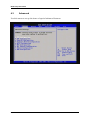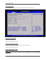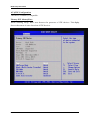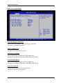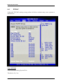
1
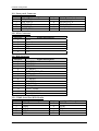
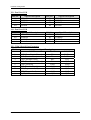
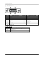
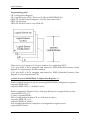
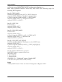
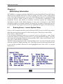
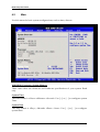
PQ7-M103XL Series User's Manual Version 1.0 Copyright © Portwell, Inc., 2010. All rights reserved. All other brand names are registered trademarks of their respective owners. Preface Table of Contents How to Use This Manual Chapter 1 System Overview ........................................................................... 1-1 1.1 Introduction ....................................................................................................... 1-1 1.2 Check List........................................................................................................... 1-1 1.3 Product Specification........................................................................................ 1-2 1.4 Mechanical Drawing......................................................................................... 1-3 1.5 System Architecture.......................................................................................... 1-4 Chapter 2 Hardware Configuration ................................................................ 2-1 2.1 Jumper Setting ................................................................................................... 2-1 2.2 Connector Allocation........................................................................................ 2-3 Chapter 3 System Installation ........................................................................ 3-1 3.1 Intel ATOM processor Z510PT/Z520PT CPU .............................................. 3-1 3.2 Intel System Controller Hub US15WPT ........................................................ 3-1 3.3 Main Memory .................................................................................................... 3-2 3.4 Installing the Single Board Computer............................................................ 3-2 3.4.1 Chipset Component Driver ................................................................... 3-2 3.4.2 Intel Integrated Graphics GMCH Chip ................................................ 3-3 3.4.3 Intel Gigabit Ethernet Controller ........................................................... 3-3 3.4.4 Audio Controller ...................................................................................... 3-3 3.5 Installing the Single Board Computer............................................................ 3-4 3.6 WDT Function ................................................................................................... 3-4 3.7 GPIO.................................................................................................................... 3-7 Chapter 4 BIOS Setup Information ................................................................ 4-1 4.1 Entering Setup -- Launch System Setup ........................................................ 4-1 4.2 Main .................................................................................................................... 4-2 4.3 Advanced ........................................................................................................... 4-3 4.4 PCIPnP.............................................................................................................. 4-17 4.5 Boot ................................................................................................................... 4-19 4.6 Security ............................................................................................................. 4-24 4.7 Chipset.............................................................................................................. 4-25 4.8 Exit..................................................................................................................... 4-30 Chapter 5 Troubleshooting ............................................................................ 5-1 5.1 Hardware Quick Installation........................................................................... 5-1 5.2 BIOS Setting ....................................................................................................... 5-2 5.3 FAQ ..................................................................................................................... 5-4 Appendix A Appendix B Preface How to Use This Manual The manual describes how to configure your PQ7-M103XL series to meet various operating requirements. It is divided into five chapters, with each chapter addressing a basic concept and operation of this QSEVEN Module. Chapter 1 : System Overview. Presents what you have in the box and give you an overview of the product specifications and basic system architecture for this model of single board computer. Chapter 2 : Hardware Configuration. Describes the definition and location for Jumpers that you can easily configure your system. Chapter 3 : System Installation. Describes the CPU, main memory SKU to get a clear information. Chapter 4 : BIOS Setup Information. Specifies the meaning of each setup parameters, how to get advanced BIOS performance and update new BIOS. In addition, POST checkpoint list will give users some guidelines of trouble-shooting. The content of this manual and EC declaration document is subject to change without prior notice. These changes will be incorporated in new editions of the document. Portwell may make supplement or change in the products described in this document at any time. Updates to this manual, technical clarification, and answers to frequently asked questions will be shown on the following web site : http://www.portwell.com.tw System Overview Chapter 1 System Overview 1.1 Introduction QSEVEN, a new industrial computer platform in “Module board” and “Carrier board” architecture, equipped processor or its socket, chipset, memory or memory socket and single Ethernet controller on it. The On-The-Shelf Module board allows users to create their own Carrier board easily and quickly since most critical parts are ready on Module board. QSEVEN Module board offers expansion interfaces such as PCI Express, SATA, LPC, LVDS, USB, SDVO and Audio etc. that could support variety functions depending on Carrier board design. The Carrier board was customized design to fit in different mechanical requirements. In the meanwhile, its variety functions were also customized to meet the application. Compares to the platform that designed from nothing, QSEVEN architecture platform only needs to develop Carrier board. Users could keep their know-how which related to their core competence in the Carrier board. PQ7-M103XL series equipped Intel eMenlow XL chipset with Atom Z510PT/Z520PT processor on-board), 512 MB DDR2 memories (up to 1GB) on-board, one Gigabit Ethernet controller on it to provide expansion interfaces – PCI Express x1. 1.2 Check List The PQ7-M103XL series package should cover the following basic items One PQ7-M103XL series module board If any of these items is damaged or missing, please contact your vendor and keep all packing materials for future replacement and maintenance. PQ7-M103XL Series User Manual 1-1 System Overview 1.3 Product Specification z Main processor - Intel® Atom Processor - FSB: Z510PT 400MHz; Z520PT 533MHz z Main Memory - Onboard DDR2 400/533 up to 1GB z L2 Cache Memory - 512K L2 Cache, Build-in processor z Chipset - Intel eMenlow (US15WPT) chipset z Expansion Interfaces - PCI Express Two PCI Express x1 links (Up to three links if no SATA demand) - LVDS Supports maximum 112MHz single channel LVDS interface Single channel LVDS interface support: 24 bpp Maximum Panel resolution supported up to 1366 x 768 - SDVO (Serial Digital Video Output) A maximum pixel clock of 160 MHz is supported on the SDVO interface. - Ethernet Intel WG82574IT Gigabit Ethernet controller is equipped - USB Interface Support eight USB 2.0 ports - IDE Interface Support 4GB NANDrive storage onboard, up to 8GB capacity. z Outline Dimension (L X W): - 70mm x 70mm z Operating Temperature: - 40°C ~ 85°C z Storage Temperature: - 40°C ~ 85°C z Relative Humidity: - 5% ~ 90%, non-condensing PQ7-M103XL Series User Manual 1-2 System Overview 1.4 Mechanical Drawing PQ7-M103XL Series User Manual 1-3 System Overview 1.5 System Architecture PQ7-M103XL Series System Block Diagram PQ7-M103XL Series User Manual 1-4 Hardware Configuration Chapter 2 Hardware Configuration This chapter gives the definitions and shows the positions of jumpers, headers and connector. All of the configuration jumpers on Portwell EVB Carrier PQ7-M103XL are in the proper position. The default settings shipped from factory are marked (Ì). 2.1 Jumper Setting Figure 2-1 PQ7-M103XL Jumper & Connector Location PQ7-M103XL Series User Manual 2-1 Hardware Configuration JP1 : LVDS Power Level JP1 1-3 3.3V Ì 3-4 12V 3-5 5V Process Selection JP2 : CPU Board BIOS Disable JP2 1-2 Function BIOS Disable JP3 : Auto Power Button selection JP3 1-2 Function Auto power button mode JP4 : RTC CMOS Clear Jumper Setting JP4 1-3、2-4 3-5、4-6 Function For com port Ì For IrDA JP5 : USB Host/Client Select JP5 1-2 2-3 Function Host Ì Client JP6 : COM2 RS232/485/422 Selection JP6 RS232 RS485 RS422 Function 5-6,9-11,10-12,15-17,16-18 Ì 1-2,7-9,8-10,19-20 3-4,7-9,8-10,13-15,14-16,21-22 JP7 : LVDS Back-light Power Level JP7 1-3,2-4 1-3,4-6 3-5,2-4 3-5,4-6 Process Selection 5V, Active High Ì 12V, Active High 5V, Active Low 12V, Active Low JP8 : CMOS Reset JP8 1-2 2-3 Function Normal Operation Ì Clear CMOS Contents PQ7-M103XL Series User Manual 2-2 Hardware Configuration 2.2 Connector Allocation I/O peripheral devices are connected to the interface connectors. Connector Function List Connector J1 J2 J3/10 J4 J5 J6 J7 J8 J11 J12 J13 J14 J15 J16 J17 J19 J20 J21 J22 J23/J24 J25 J26 J27 J28 Function LVDS Panel Back-light Power Connector RTC Battery Connector SATA Interface Connector Power Header LVDS Connector 4P Power Connector for 12V 3P FAN Power Connector (System) Audio Header 8-Bit GPIO Header Mini-PCI E Connector LPC Debug Port MXM Connector SD Card Slot Dual Port USB Header (Only USB2.0 Device) Client USB Header Front Panel Control Header IrDA Connector RJ45 Lan Port COM2 Serial Port BOX Header Dual Port USB COM 1 Serial Port Connector D-Sub15 VGA Connector DC Jack 12V Reserve Header Remark Pin Assignments of Connectors PQ7-M103XL Series User Manual 2-3 Hardware Configuration J1 : LVDS Panel Back-light Power Connector PIN No. 1 2 3 4 5 Signal Description Backlight Power Ground +12V L_BKLTCTL +5V J2 : RTC Battery Connector PIN No. 1 2 Signal Description Positive Negative J3/10 : SATA Interface Connector PIN No. 1 2 3 4 5 6 7 Signal Description GND GND SATA_TXP0 SATA_TXP1 SATA_TXN0 SATA_TXN1 GND GND SATA_RXN0 SATA_RXN1 SATA_RXP0 SATA_RXP1 GND GND J4 : Power Header PIN No. 1 2 3 4 Signal Description V12 GND GND VCC PQ7-M103XL Series User Manual 2-4 Hardware Configuration J5 : LVDS Panel Connector PIN No. 1 3 5 7 9 11 13 15 17 19 21 23 25 27 29 Signal Description VDD_LVDS DF_LA_DATA+0 DF_LA_DATA+1 DF_LA_DATA+2 DF_LA_DATA+3 DF_LA_CLK+ L_CTLA_CLK GND DF_LB_DATA+0 DF_LB_DATA+1 DF_LB_DATA+2 DF_LB_DATA+3 DF_LB_CLK+ N/A GND PIN No. 2 4 6 8 10 12 14 16 18 20 22 24 26 28 30 Signal Description VDD_LVDS DF_LA_DATA-0 DF_LA_DATA-1 DF_LA_DATA-2 DF_LA_DATA-3 DF_LA_CLKL_CTLB_DATA GND DF_LB_DATA-0 DF_LB_DATA-1 DF_LB_DATA-2 DF_LB_DATA-3 DF_LB_CLKN/A GND J6 : 4P Power Connector for 12V 1 2 3 4 PIN No. 1 2 3 4 Signal Description Ground Ground +12V +12V J7 : 3P FAN Power Connector 1 2 3 PIN No. 1 2 3 Signal Description Ground +12V Fan Speed Detecting signal PQ7-M103XL Series User Manual 2-5 Hardware Configuration J8 : Audio Header PIN No. 1 2 3 4 5 6 7 8 9 10 Signal Description CN_MIC-R AGND CN_MIC-L AGND CN_LINOUT-R NC VCC CN_LINOUT-L NC J11 : 8-Bit GPIO Header PIN No. 1 3 5 7 9 Signal Description SIO_GPIO0 SIO_GPIO1 SIO_GPIO2 SIO_GPIO3 Ground PIN No. 2 4 6 8 10 Signal Description SIO_GPIO4 SIO_GPIO5 SIO_GPIO6 SIO_GPIO7 VCC PIN No. 2 4 6 8 10 12 14 16 18 20 22 24 26 28 30 32 34 36 Signal Description VCC3 GND VCC1_5 N/C N/C N/C N/C N/C GND N/C RST# 3.3VAUX GND VCC1_5 SMB_CLK SMB_DAT GND DF_USB_PN0 J12 : Mini-PCIE Slot PIN No. 1 3 5 7 9 11 13 15 17 19 21 23 25 27 29 31 33 35 Signal Description PCIE_WAKE# N/C N/C CLKREQ# GND DF_CLK_PCIE# DF_CLK_PCIE GND N/C N/C GND DF_PCIE_RXN1 DF_PCIE_RXP1 GND GND DF_PCIE_TXN1 DF_PCIE_TXP1 GND PQ7-M103XL Series User Manual 2-6 Hardware Configuration 37 39 41 43 45 47 49 51 N/C N/C N/C N/C N/C N/C N/C N/C 38 40 42 44 46 48 50 52 DF_USB_PP0 GND N/C N/C N/C VCC1_5 GND VCC3 J13 : LPC Debug Port PIN No. 1 3 5 7 9 Signal Description LPC_AD0 LPC_AD1 LPC_AD2 LPC_AD3 PQ7-M103XL Series User Manual PIN No. 2 4 6 8 10 Signal Description VCC3 RST# LPC_FRAME# CLK_LPC_FWH GND 2-7 Hardware Configuration J14 : MXM Connector PIN No. 1 3 5 7 9 11 13 15 17 19 21 23 25 27 29 31 33 35 37 39 41 43 45 47 49 51 53 55 57 59 61 63 65 67 69 71 73 75 77 79 81 Signal Description GND DF_LAN1_MDIN3 DF_LAN1_MDIP3 LAN1_LINK100DF_LAN1_MDIN1 DF_LAN1_MDIP1 LAN1_LINK# VCTREF_GBE0_CT LPC_PME# VSB3 SLP_BTN# (not implement) GND GND BATLOW# (not implement) DF_SATA0_TX+ DF_SATA0_TXSATA_ACT# DF_SATA0_RX+ DF_SATA0_RXGND BIOS_DISABLE# SLOT2_CD# SLOT2_CMD SD2PWR# SLOT2_DATA0 SLOT2_DATA2 SLOT2_DATA4 SLOT2_DATA6 GND HAD_SYNC HAD_RST# HAD_BITCLK HAD_SDATAIN0 HAD_SDATAOUT PM_THRM# THERMTRIP# GND DF_USB_PN7 DF_USB_PP7 USB_6_7_OC# DF_USB_PN5 PQ7-M103XL Series User Manual PIN No. 2 4 6 8 10 12 14 16 18 20 22 24 26 28 30 32 34 36 38 40 42 44 46 48 50 52 54 56 58 60 62 64 66 68 70 72 74 76 78 80 82 Signal Description GND DF_LAN1_MDIN2 DF_LAN1_MDIP2 LAN1_LINK1000DF_LAN1_MDIN0 DF_LAN1_MDIP0 LAN1_ACTSLP_S5# SLP_S3# PWRBTN#_PM LID_BTN# (not implement) GND PWROK_Q7 RST_SYS# DF_SATA1_TX+ DF_SATA1_TXGND DF_SATA1_RX+ DF_SATA1_RXGND SLOT2_CLK SD2_LED SLOT2_WP SLOT2_DATA1 SLOT2_DATA3 SLOT2_DATA5 SLOT2_DATA7 RSVD GND SMB_CLK SMB_DATA SMB_ALERT# I2C_CLK I2C_DAT WDTRIG# WDOUT (not implement) GND DF_USB_PN6 DF_USB_PP6 USB_4_5_OC# DF_USB_PN4 2-8 Hardware Configuration 83 85 87 89 91 93 95 97 99 101 103 105 107 109 111 113 115 117 119 121 123 125 127 129 131 133 135 137 139 141 143 145 147 149 151 153 155 157 159 161 163 165 167 169 171 DF_USB_PP5 USB_2_3_OC DF_USB_PN3 DF_USB_PP3 USB_HOST_PRES# DF_USB_PN1 DF_USB_PP1 GND LA_DATAP0 LA_DATAN0 LA_DATAP1 LA_DATAN1 LA_DATAP2 LA_DATAN2 L_VDDEN LA_DATAP3 LA_DATAN3 GND DF_LA_CLKP DF_LA_CLKN L_BKLTCTL LVDS_DID_DAT LVDS_DID_ CLK RSVD SDVO_CLK+ SDVO_CLKGND SDVO_GREEN+ SDVO_GREENGND SDVO_BLUE+ SDVO_BLUEGND SDVO_RED+ SDVO_REDN/C DF_CLK_PCIE+ DF_CLK_PCIEGND PCIE_TX3+ (not implement) PCIE_TX3- (not implement) GND PCIE_TX2+ (not implement) PCIE_TX2- (not implement) EXCD0_PERST# PQ7-M103XL Series User Manual 84 86 88 90 92 94 96 98 100 102 104 106 108 110 112 114 116 118 120 122 124 126 128 130 132 134 136 138 140 142 144 146 148 150 152 154 156 158 160 162 164 166 168 170 172 DF_USB_PP4 USB_0_1_OC# DF_USB_PN2 DF_USB_PP2 USB_HC_SEL DF_USB_PN0 DF_USB_PP0 GND LB_DATAP0 (not implement) LB_DATAN0 (not implement) LB_DATAP1 (not implement) LB_DATAN1 (not implement) LB_DATAP2 (not implement) LB_DATAN2 (not implement) L_BKLTEN LB_DATAP3 (not implement) LB_DATAN3 (not implement) GND DF_LB_CLKP (not implement) DF_LB_CLKN (not implement) RSVD LVDS_BLC_DAT LVDS_BLC_CLK RSVD SDVO_INT+ SDVO_INTGND SDVO_FLDSTALL+ SDVO_FLDSTALLGND SDVO_TVCLKIN+ SDVO_TVCLKINGND SDVO_CTRLDATA SDVO_CTRLCLK N/C PCIE_WAKE# RST# GND PCIE_RX3+(not implement) PCIE_RX3- (not implement) GND PCIE_RX2+(not implement) PCIE_RX2- (not implement) EXCD1_PERST# 2-9 Hardware Configuration 173 175 177 179 181 183 185 187 189 191 193 195 197 199 201 203 205 207 209 211 213 215 217 219 221 223 225 227 229 PCIE_TX1+ PCIE_TX1EXCD0_CPPE# (not implement) PCIE_TX0+ PCIE_TX0GND LPC_AD0 LPC_AD2 CLK_LPC_FWH LPC_SERIRQ V3.3A_RTC FAN_TACHOIN (not implement) GND RSVD RSVD (use for A20M#) RSVD VSB5 MFG_N/C MFG_N/C VCC VCC VCC VCC VCC VCC VCC VCC VCC VCC PQ7-M103XL Series User Manual 174 176 178 180 182 184 186 188 190 192 194 196 198 200 202 204 206 208 210 212 214 216 218 220 222 224 226 228 230 PCIE_RX1+ PCIE_RX1EXCD1_CPPE# (not implement) PCIE_RX0+ PCIE_RX0GND LPC_AD1 LPC_AD3 LPC_FRAME# LPC_LDRQ#(not implement) SPKR FAN_PWMOUT (no implement GND RSVD RSVD MFG_N/C VSB5 MFG_N/C MFG_N/C VCC VCC VCC VCC VCC VCC VCC VCC VCC VCC 2-10 Hardware Configuration J15 : SD Card Slo PIN No. Signal Description 1 DAT3 2 CMD_RSP 3 GND 4 VCC 5 CLK 6 GND 7 DAT0 8 DAT1 9 DAT2 Sa WP# Sb CD# Sc CD#_COM J16 : Dual Port USB Header(Only USB2.0 Device) 10 2 1 PIN No. 1 3 5 7 7 Signal Description +5V USBD6N USBD6P Ground PIN No. 2 4 6 8 10 Signal Description +5V USBD7N USBD7P Ground NC J17 : Client USB Header 10 2 1 PIN No. 1 3 5 7 7 Signal Description +5V USBD1N USBD1P Ground PQ7-M103XL Series User Manual PIN No. 2 4 6 8 10 Signal Description NC NC NC NC NC 2-11 Hardware Configuration J19 : Front panel Connector PIN No. 1 3 5 7 9 Signal Description HD_LED_P HD_LED_N RST_SW_N RST_SW_P RSVD_DNU PIN No. 2 4 6 8 10 Signal Description FP PWR/SL_P FP PWR/SL_N PWR_SW_P PWR_SW_N J20 : IrDA Connector PIN No. 1 2 3 4 5 6 Signal Description IRRX Ground Ground NC IRTX VCC J21 : RJ45 LAN Port PIN No. 1 2 3 4 5 6 7 8 9 10 11 12 13 14 Signal Description L1_MDIP0 L1_MDIN0 L1_MDIP1 L1_MDIN1 VCTREF_GBE0_CT GND L1_MDIP2 L1_MDIN2 L1_MDIP3 L1_MDIN3 LAN1_ACTLAN1_LINK# LAN1_LINK1000LAN1_LINK100- J22 : COM2 Serial Port BOX Header PIN No. 1 3 5 7 9 Signal Description DCD#2 RXD#2 TXD#2 DTR#2 GND PQ7-M103XL Series User Manual PIN No. 2 4 6 8 10 Signal Description DSR#2 RTS#2 CTS#2 RI#2 2-12 Hardware Configuration J23 : Dual Port USB PIN No. A1 A2 A3 A4 Signal Description +5V USBD3N USBD3P Ground PIN No. B1 B2 B3 B4 Signal Description +5V USBD2N USBD2P Ground PIN No. B1 B2 B3 B4 Signal Description J24 : Dual Port USB PIN No. A1 A2 A3 A4 Signal Description +5V USBD5N USBD5P Ground +5V USBD4N USBD4P Ground J25 : COM 1 Serial Port Connector PIN No. 1 2 3 4 5 6 7 8 9 Signal Description RS-232 RS-422 DCD (Data Carrier Detect) TXRXD (Receive Data) TX+ TXD (Transmit Data) RX+ DTR (Data Terminal Ready) RXGND (Ground) GND DSR (Data Set Ready) N/C RTS (Request to Send) N/C CTS (Clear to Send) N/C RI/5V/12V N/C PQ7-M103XL Series User Manual RS-485 DATADATA+ N/C N/C GND N/C N/C N/C N/C 2-13 Hardware Configuration J26 : D-SUB15 VGA Connector 5 1 10 6 15 PIN No. 1 3 5 7 9 11 13 15 11 Signal Description RED BLUE Ground Ground NC ID1 HSYNC DDCCLK PIN No. 2 4 6 8 10 12 14 Signal Description GREEN ID0 Ground Ground Ground DDCDATA VSYNC J27 : DC Jack 12V PIN No. 2 3 4 Signal Description V12CON_IN GND GND PQ7-M103XL Series User Manual 2-14 System Installation Chapter 3 System Installation This chapter provides you with instructions to set up your system. The additional information is enclosed to help you set up onboard PCI device and handle Watch Dog Timer (WDT) and operation of GPIO in software programming. 3.1 Intel ATOM processor Z510PT/Z520PT CPU Configuring System Bus PQ7-M103XL will automatically detect the CPU FSB 400/533MHz CMOS used. CPU speed of Intel ATOM Processor for Mobile can be detected automatically. 3.2 Intel System Controller Hub US15WPT The Intel® System Controller Hub US15WPT is a low-power chipset in one small 22x22mm package; it combines the Intel® Graphics Media Accelerator 500, memorycontroller, and I/O controller in a single-chip solution while featuring advanced 3D graphics and extensive I/O capabilities such as USB2.0, SDIO and PCI Express. It supports Intel® High Definition Audio and hardware video decode acceleration, a 400/533 MHz CMOS front-side bus, dual independent display. PQ7-M103XL Series User Manual 3-1 System Installation 3.3 Main Memory PQ7-M103XL provides 1 GBytes of on-board DDR2-SDRAM as main memory. Memory clock and related settings can be detected by BIOS via SPD interface. Memory frequency / CPU FSB synchronization PQ7-M103XL supports different memory frequencies depending on the CPU front side bus and the type of DDR2-SDRAM. CPU FSB 533MHz 400MHz 3.4 Memory Frequency 533MHz 400MHz Installing the Single Board Computer To install your PQ7-M103XL into standard chassis or proprietary environment, please perform the following: Step 1 : Check all jumpers setting on proper position Step 2 : Install and configure CPU and memory module on right position Step 3 : Place PQ7-M103XL into the dedicated position in the system Step 4 : Attach cables to existing peripheral devices and secure it WARNING Please ensure that SBC is properly inserted and fixed by mechanism. Note: Please refer to section 3.4.1 to 3.4.4 to install INF/VGA/LAN/Audio drivers 3.4.1 Chipset Component Driver The chipset on PQ7-M103XL is a new chipset that a few old operating systems might not be able to recognize. To overcome this compatibility issue, for Windows Operating Systems such as Windows XP/VISTA, please install its INF before any of other Drivers are installed. You can find very easily this chipset component driver in PQ7-M103XL CD-title. PQ7-M103XL Series User Manual 3-2 System Installation 3.4.2 Intel Integrated Graphics GMCH Chip Using Intel® SCH US15WPT with Media Accelerator High performance graphic integrated chipset is aimed to gain an outstanding graphic performance. Shared 1MB to 8MB system DDR2-SDRAM Memory with Total Graphics Memory. This combination makes PQ7-M103XL an excellent piece of multimedia hardware. Drivers Support Please find Springdale GMCH driver in the PQ7-M103XL CD-title. Drivers support Windows XP / VISTA. 3.4.3 Intel Gigabit Ethernet Controller Drivers Support Please find WG82574IT LAN driver in /Ethernet directory of PQ7-M103XL CD-title. The drivers support Windows XP / VISTA. LED Indicator (for LAN status) PQ7-M103XL provides two LED indicators to report WG82574IT Gigabit Ethernet interface status. Please refer to the table below as a quick reference guide. Intel 82574IT Color Name of LED Status LED Green Linked & Active LED Speed LED Orange Green Speed LED Operation of Ethernet Port Linked Active On Blinking Giga Mbps 100 Mbps 10 Mbps Orange Green Off 3.4.4 Audio Controller Please find Realtek ALC262 Audio driver form PQ7-M103XL CD-title. The drivers support Windows XP / VISTA. PQ7-M103XL Series User Manual 3-3 System Installation 3.5 Installing the Single Board Computer The following table indicates how to enable/disable Clear CMOS Function hardware circuit by putting jumpers at proper position. JP8 : CMOS Reset JP8 Function 1-2 Normal Operation Ì 2-3 Clear CMOS Contents To correctly operate CMOS Clear function, users must turn off the system, move JP8 jumper to short pin 2 and 3. Move the JP8 back to 1-2 position (Normal Operation) and start the system. System will then produce a “CMOS Check Sum Error” message and hold up. Users may then follow the displayed message to load BIOS default setting. 3.6 WDT Function The algorithm of the WDT function can be simply described as a timer counting process with an output event. The Time-Out period ( Twd ) can be set by software commands or hardware jumpers that depend on the board circuit design and may be different among the boards. This timer can be used to monitor a software hang. PQ7-M103XL allows users to control WDT by issuing dynamic software commands. The WDT starts counting when it is activated. It will cause a system reset once it expires. Before WDT expires, a refreshing command with a Twd can be issued to re-count WDT and continue the status monitoring. If the system encounters a software or application hang, WDT will generate a system reset after its timeout. The related Control Registers of WDT are included in the following programming guide that is written in C language. User can write a non-zero value ( defined as Twd ) into the Time-out Value Register ( CR_Twd ) to enable WDT. Users can write 0x00 and then Twd to CR_Twd to refresh WDT. To refresh WDT, the time tolerance of refreshing interval must be considered. The smaller of Twd, the more deviation of WDT and you need to include more tolerance. “Let Twd be longer than 2 seconds” is the recommendation due to the limitation of Winbond W83627DHG WDT. You can call Portwell support center for reference. The value read back from CR_Twd indicates the counting down value instead of the original Twd. System will be reset after the Time-out Value to be counted down to zero. Users can directly fill a zero value into CR_Twd to disable WDT immediately. To ensure a successful access to the desired Control Register, the following programming guide should be followed. PQ7-M103XL Series User Manual 3-4 System Installation Programming guide: CR: Configuration Register. LD: Logical Device of SIO. There are 12 LDs in W83627DHG SIO. CR00~2F: Global Control Registers. (All LDs share these CRs ) CR07: LD selection. CR30~FF: Each LD has its own CR30~FF. There are two I/O ports as I/O access window for configuring WDT, 1) IO port 0x2E is H/W strapped and named as EFIR (Extended Function Index Register, for identifying CR index number) 2) IO port 0x2F is H/W strapped and named as EFDR (Extended Function Data Register, for accessing desired CR) << How to access W83627DHG Configuration Register >> First, it needs to enter extended function mode. Enter extended function mode for accessing W83627DHG configuration registers: outportb (EFIR, 0x87); outportb (EFIR, 0x87); // double IO write Read Configuration Register CR_rx, and keep this byte to unsigned char al_char outportb(EFIR, CR_rx ) ; al_char = inportb(EFDR) ; Write Configuration Register CR_wx with byte al_char1 ; outportb (EFIR, CR_wx ) ; outportb (EFDR, al_char1); Exit extended mode after completion of configuration register access. outportb(EFIR, 0xaa); PQ7-M103XL Series User Manual 3-5 System Installation << How to access W83627DHG WDT Configuration Register >> Must enter extended function mode first, then follow the following steps for accessing WDT registers. Step (1): CR2D_bit0P0 Initialize the multiplex pin (pin77) to WDTO function outportb ( EFIR , 0x2D ) ; // al_char1 : unsigned char al_char1 = inportb (EFDR) & 0xFE; // CR2D_bit0P0 outportb ( EFIR , 0x2D ) ; // init pin 77 to WDT outportb ( EFDR , al_char1 ) ; Step (2) : CR07_P08 Ponit to LD8. outportb ( EFIR , 0x07 ) ; outportb ( EFDR , 0x08 ) ; Step (3) : LD8_CR30_bit0P1 Activate LD8 outportb ( EFIR , 0x30 ) ; al_char1 = inportb ( EFDR ) | 0x01 ; // CR30_bit0P1 outportb ( EFIR , 0x30 ) ; // Activate LD8 outportb ( EFDR , al_char1 ) ; Step (4) : LD8_CRF7_bit[7,6]P[0,0] Not allow K/B and Mouse’s interrupts to reload WDT timer. outportb ( EFIR , 0xF7 ) ; al_char1 = inportb ( EFDR ) & 0x3F ; // CRF7_bit[7,6]P[0,0] outportb ( EFIR , 0xF7 ) ; outportb ( EFDR , al_char1 ) ; Step (5) : Refresh WDT before it expires. Once WDT expires, system will be reset. LD8_CRF5_bit3 : 0 : Second Mode 1 : Minute Mode LD8_CRF6: Twd , “Writing 00” means “disable WDT” 1~255 time unit (time unit: second, minute) Notes: “CR2D_bit0P0“means” Write 0 to bit0 of Configuration Register 0x2D”. PQ7-M103XL Series User Manual 3-6 System Installation 3.7 GPIO The PQ7-M103XL provides 8 programmable input or output ports that can be individually configured to perform a simple basic I/O function. Users can configure each individual port to become an input or output port by programming register bit of I/O Selection. To invert port value, the setting of Inversion Register has to be made. Port values can be set to read or write through Data Register. The GPIO ports are located on J12 shown as follows. Notes : Do not short-circuit Pin 9 and 10 of J11! J11: GPIO Connector (2*5 Pin Header) J11: General Purpose I/O Connector PIN No. 1 3 5 7 9 Signal Description GPIO0 GPIO1 GPIO2 GPIO3 Ground PQ7-M103XL Series User Manual PIN No. 2 4 6 8 10 Signal Description GPIO4 GPIO5 GPIO6 GPIO7 +5V 3-7 System Installation Programming Guide: Must enter extended function mode (Double I/O write 0x87 to EFIR) first, then follow the following steps for accessing GPIO pins. When completion of GPIO access, Exit extended mode (I/O write 0xaa to EFIR). Initialize W83627DHG multiplex pins as GPIO30~37 pins CR2C_bit[7:5]P[0,0,0] outportb ( EFIR , 0x2C ) ; // al_char1 : unsigned char al_char1 = inportb ( EFDR ) | 0x02 ; // CR2C_bit[7:5]P[0,0,0] outportb ( EFIR , 0x2C ) ; // init GP30~37 function outportb ( EFDR , al_char1 ) ; Point to LD9 and activate its function CR07_P09 ; Point to LD9 outportb ( EFIR , 0x09 ) ; outportb ( EFDR , 0x09 ) ; LD9_CR30_bit1P1 ; Activate LD9 outportb ( EFIR , 0x30 ) ; al_char1 = inportb ( EFDR ) | 0x02 ; // CR30_bit1P1 outportb ( EFIR , 0x30 ) ; // Activate LD9 outportb ( EFDR , al_char1 ) ; (1) LD9_CRF2_PFF ; Inverse input/output signals outportb ( EFIR , 0xF2 ) ; outportb ( EFDR , 0xFF ) ; (2) LD9_CRF0_PF0 ; Set GP30~33 as input pins and GP34~37 as output pins outportb ( EFIR , 0xF0 ) ; outportb ( EFDR , 0xF0 ) ; (3) LD9_CRF1 ; Data Register for reading/writing data to GPIO pins ; E.g. if put four jumper caps on J12 pin1-2,3-4,5-6,and 7-8 ; ( Warning : J22 pin9-10 is not allowed to be short circuit. ) ; and then Write [1,0,1,0] to bit[3:0] , you can get [1,0,1,0] ; from bit[7:4]. PQ7-M103XL Series User Manual 3-8 BIOS Setup Information Chapter 4 BIOS Setup Information PQ7-M103XL is equipped with the AMI BIOS stored in Flash ROM. These BIOS has a built-in Setup program that allows users to modify the basic system configuration easily. This type of information is stored in CMOS RAM so that it is retained during power-off periods. When system is turned on, PQ7-M103XL communicates with peripheral devices and checks its hardware resources against the configuration information stored in the CMOS memory. If any error is detected, or the CMOS parameters need to be initially defined, the diagnostic program will prompt the user to enter the SETUP program. Some errors are significant enough to abort the start up. 4.1 Entering Setup -- Launch System Setup Power on the computer and the system will start POST (Power On Self Test) process. When the message below appears on the screen, press <Del> key to enter Setup. Press <Del> to enter SETUP If the message disappears before you respond and you still wish to enter Setup, restart the system by turning it OFF and On or pressing the RESET button. You may also restart the system by simultaneously pressing <Ctrl>, <Alt>, and <Delete> keys. Press <F1> to Run SETUP or Resume The BIOS setup program provides a General Help screen. You can call up this screen from any menu by simply pressing <F1>. The Help screen lists the appropriate keys to use and the possible selections for the highlighted item. Press <Esc> to exit the Help screen. PQ7-M103XL Series User Manual 4-1 BIOS Setup Information 4.2 Main Use this menu for basic system configurations, such as time, date etc. AMI BIOS, Processor, System Memory These items show the firmware and hardware specifications of your system. Read only. System Time The time format is <Hour> <Minute> <Second>. Use [+] or [-] to configure system Time. System Date The date format is <Day>, <Month> <Date> <Year>. Use [+] or [-] to configure system Date. PQ7-M103XL Series User Manual 4-2 BIOS Setup Information 4.3 Advanced Use this menu to set up the items of special enhanced features. PQ7-M103XL Series User Manual 4-3 BIOS Setup Information CPU Configuration These items show the advanced specifications of your CPU. Read only. Max CPUID Value Limit Disabled for Windows XP The choice: Disabled, Enabled. Execute-Disable Bit capability When disabled, force the XD feature flag to always return 0 The choice: Disabled, Enabled. Hyper Threading Technology Enable for Windows XP and Linux4 (OS optimized for Hyper Threading Technology) and disabled for other OS (OS not optimized for Hyper-Threading Technology) PQ7-M103XL Series User Manual 4-4 BIOS Setup Information Intel(R) Speed Step (tm) Tech Disable: Disable GV3. Enable: Enable GV3. The choice: Disabled, Enabled. Intel(R) C-STATE Tech CPU idle is set to C2, C3, C4 State. The choice: Disabled, Enabled. IDE Configuration The IDE Configuration the IDE devices, such as hard disk drive or CD-ROM drive. It uses a separate sub menu to configure each hard disk drive (Master and Slave). PQ7-M103XL Series User Manual 4-5 BIOS Setup Information ATA/IDE Configuration The choice: Disabled, Compatible. Primary IDE Master/Slave While entering setup, BIOS auto detects the presence of IDE devices. This display shows the status of auto detection of IDE devices. PQ7-M103XL Series User Manual 4-6 BIOS Setup Information [Type] Press PgUp/<+> or PgDn/<-> to select [Manual], [None] or [Auto] type. You can use [Manual] to define your own drive type manually. [LBA/Large Mode] Enabling LBA causes Logical Block Addressing to be used in place of Cylinders, Heads and Sectors. [Block (Multi-Sector Transfer)] Any selection except Disabled determines the number of sectors transferred per block. [PIO Mode] Indicates the type of PIO (Programmed Input/Output) [DMA Mode] Indicates the type of Ultra DMA [S.M.A.R.T.] This allows you to activate the S.M.A.R.T. (Self-Monitoring Analysis & Reporting Technology) capability for the hard disks. S. M.A.R.T is a utility that monitors your disk status to predict hard disk failure. This gives you an opportunity to move data from a hard disk that is going to fail to a safe place before the hard disk becomes offline. [32 Bit Data Transfer] Enable/Disable 32-bit Data Transfer. Hard Disk Write Protect Disabled/Enabled device write protection, this will be effective only if device is accessed through BIOS. The choice: Disabled, Enabled. IDE Detect Time Out (Sec) Select the time out value for detecting ATA/ATAPI device (s). The choice: 0, 5, 10, 15, 20, 25, 30, 35. ATA(PI) 80Pin Cable Detection Select the mechanism for detecting 80Pin ATA (PI) cable. The choice: Host & Device, Host, Device. JMicron 36x ATA Controller Select ATA Controller Operate Mode The choice: Disabled, IDE Mode, AHCI+IDE Mode. PQ7-M103XL Series User Manual 4-7 BIOS Setup Information Super IO Configuration Onboard Floppy Controller Allows BIOS to Enable or Disable Floppy controller. The choice: Disabled, Enabled. Floppy Mode Select The choice: Normal, Write Protect Serial Port 1 Address Allows BIOS Select Serial Port1 Base Addresses. The choice: Disabled, 3F8/IRQ4, 3E8/IRQ4, 2E8/IRQ3. Serial Port 2 Address Allows BIOS Select Serial Port2 Base Addresses. The choice: Disabled, 2F8/IRQ3, 3E8/IRQ4, 2E8/IRQ3. Serial Port 2 Mode Allows BIOS Select mode for Serial Port2. The choice: Normal, IrDA, ASK IR. PQ7-M103XL Series User Manual 4-8 BIOS Setup Information Parallel Port Address Allows BIOS to Select Parallel Port Base Addresses. The choice: Disabled, 378, 278, 3BC. Parallel Port Mode Allows BIOS to Select Parallel Port mode. The choice: Normal, Bi-Directional, ECP, EPP, ECP &EPP. Parallel Port IRQ Allows BIOS to Select Parallel Port IRQ. The choice: IRQ5, IRQ7. ACPI Settings PQ7-M103XL Series User Manual 4-9 BIOS Setup Information General ACPI Configuration Suspend mode Select the ACPI state used for System Suspend. [S3 (STR)] The S3 sleep mode is a lower power state where the information of system configuration and open applications/ files is saved to main memory that remains powered while most other hardware components turn off to save energy. The information stored in memory will be used to restore the system when a “wake up” event occurs. The choice: S3 (STR) PQ7-M103XL Series User Manual 4-10 BIOS Setup Information Repost Video on S3 Resume Determines whether to invoke VGA BIOS post on S3/STR resume. The choice: No, Yes Advanced ACPI Configuration Advanced ACPI Configuration settings, Use this section to configure additional ACPI options. ACPI Version Features Enable RSDP pointers to 64-bit Fixed System Description Tables. The choice: ACPI v1.0 / ACPI v2.0 / ACPI v3.0. ACPI APIC support Include ACPI APIC table pointer to RSDT pointer list. The choice: Disabled, Enabled. PQ7-M103XL Series User Manual 4-11 BIOS Setup Information AMI OEMB table Include OEMB table pointer to R(X) SDT pointer list. The choice: Disabled, Enabled. Headless mode Enable / Disable Headless operation mode through ACPI. The choice: Disabled, Enabled. South Bridge ACPI Configuration The South Bridge ACPI related Configuration settings, Use this section to configure additional ACPI options. PQ7-M103XL Series User Manual 4-12 BIOS Setup Information APIC ACPI SCI IRQ Enable / Disable APIC ACPI SCI IRQ. The choice: Disabled, Enabled. USB Device Wakeup From S3/S4 Enable / Disable USB device Wake from S3/S4 mode. The choice: Disabled, Enabled. MPS Configuration Configure the Multi-Processor Table. PQ7-M103XL Series User Manual 4-13 BIOS Setup Information MPS Revision This field allows you to select which MPS (Multi-Processor Specification) version to be used for the operating system. You need to select the MPS version supported by your operating system. To find out which version to use, consult the vendor of your operating system. The choice: 1.1, 1.4. PCI Express Configuration PCI Express Configuration Menu Active State Power-Management Enable/Disable PCI Express L0s and L1 link power states. The choice: Disabled, Enabled. PQ7-M103XL Series User Manual 4-14 BIOS Setup Information Smbios Configuration SMBIOS Configuration Menu Smbios Smi Support SMBIOS SMI Wrapper support for PnP Function 50h-54h The choice: Disabled, Enabled. PQ7-M103XL Series User Manual 4-15 BIOS Setup Information USB Configuration Legacy USB Support Enables support for legacy USB. AUTO option disables legacy support if no USB devices are connected. The choice: Disabled, Enabled, Auto. USB 2.0 Controller Mode Configures the USB 2.0 controller in HiSpeed (480Mbps) or FullSpeed (12Mbps). The choice: FullSpeed, HiSpeed. BIOS EHCI Hand-Off This is a workaround for OSes without EHCI hand-off support. The EHCI ownership change should claim by EHCI driver. The choice: Disabled, Enabled. PQ7-M103XL Series User Manual 4-16 BIOS Setup Information 4.4 PCIPnP Advanced PCI/PnP setting wrong values in below sections may cause system to malfunction. Clear NVRAM Clear NVRAM during System Boot. The choice: No, Yes. PQ7-M103XL Series User Manual 4-17 BIOS Setup Information Plug & Play O/S No: lets the BIOS configure all the devices in the system. Yes: lets the operating system configure Plug and Play (PnP) devices not required for boot if your system has a Plug and Play operating system. The choice: No, Yes. PCI Latency Timer Select value in units of PCI clocks for PCI device latency timer register. The choice: 32, 64, 96, 128, 160, 192, 224, 248. Allocate IRQ to PCI VGA Yes: Assigns IRQ to PCI VGA card if card requests IRQ. No: Does not assign IRQ to PCI VGA card if card requests an IRQ. The choice: Yes, No. Palette Snooping Enabled: Informs the PCI devices that an ISA graphics device is installed in the system so the card will function correctly. The choice: Disabled, Enabled. PCI IDE BusMaster Enabled: BIOS Uses PCI busmastering for reading / writing to IDE drives. The choice: Disabled, Enabled. OffBoard PCI/ISA IDE Card Some PCI IDE cards may require this to be set to the PCI slot number that is holding the card. AUTO: Works for most PCI IDE cards The choice: Auto, PCI Slot1, PCI Slot2, PCI Slot3, PCI Slot4, PCI Slot5, PCI Slot6. PQ7-M103XL Series User Manual 4-18 BIOS Setup Information IRQ 3 / IRQ 4 / IRQ5 / IRQ7 / IRQ 9 / IRQ 10 / IRQ 11 / IRQ 14 / IRQ 15 Available: Specified IRQ is available to be used by PCI/PnP devices. Reserved: Specified IRQ is reserved for used by Legacy ISA devices. The choice: Available, Reserved. Reserved Memory Size Select Size of memory block to reserve for legacy ISA devices. The choice: Disabled, 16K, 32K, 64K. 4.5 Boot Use this menu to specify the priority of boot devices. PQ7-M103XL Series User Manual 4-19 BIOS Setup Information Boot Settings Configuration Configure Settings during System Boot. Quick Boot Allows BIOS to skip certain tests while booting. This will decrease the time needed to boot the system. The choice: Disabled, Enabled. PQ7-M103XL Series User Manual 4-20 BIOS Setup Information Quiet Boot This BIOS feature determines if the BIOS should hide the normal POST messages with the motherboard or system manufacturer's full-screen logo. When it is enabled, the BIOS will display the full-screen logo during the boot-up sequence, hiding normal POST messages. Disabled: Displays normal POST messages. Enabled: Displays OEM Logo instead of POST messages. Please note that enabling this BIOS feature often adds 2-3 seconds of delay to the booting sequence. This delay ensures that the logo is displayed for a sufficient amount of time. Therefore, it is recommended that you disable this BIOS feature for a faster boot-up time. The choice: Disabled, Enabled. AddOn ROM Display Mode Set display mode for Option ROM. This item is used to determine the display mode when an optional ROM is initialized during POST. When set to [Force BIOS], the display mode used by AMI BIOS is used. Select [Keep Current] if you want to use the display mode of optional ROM. The choice: Force BIOS, Keep Current. Bootup Num-Lock Select Power-on state for Numlock. Setting to [On] will turn on the Num Lock key when the system is powered on. Setting to [Off] will allow users to use the arrow keys on the numeric keypad. The choice: Off, On. Wait For ‘F1’ If Error Wait for F1 key to be pressed if error occurs. When this setting is set to [Enabled] and the boot sequence encounters an error, it asks you to press F1. If disabled, the system continues to boot without waiting for you to press any keys. The choice: Disabled, Enabled. Hit ‘DEL’ Message Display Displays “Press Del to run Setup” in POST. The choice: Disabled, Enabled. PQ7-M103XL Series User Manual 4-21 BIOS Setup Information Interrupt 19 Capture Interrupt 19 is the software interrupt that handles the boot disk function. When enabled, this BIOS feature allows the ROM BIOS of these host adaptors to "capture" Interrupt 19 during the boot process so that drives attached to these adaptors can function as bootable disks. In addition, it allows you to gain access to the host adaptor's ROM setup utility, if one is available. When disabled, the ROM BIOS of these host adaptors will not be able to "cap ture" Interrupt 19. Therefore, you will not be able to boot operating systems from any bootable disks attached to these host adaptors. Nor will you be able to gain access to their ROM setup utilities. The choice: Disabled, Enabled. Boot Device Priority PQ7-M103XL Series User Manual 4-22 BIOS Setup Information 1st Boot Device The items allow you to set the sequence of boot devices where BIOS attempts to load the disk operating system. First press <Enter> to enter the sub-menu. Then you may use the arrow keys (↑↓) to select the desired device, then press <+>, <-> or <PageUp>, <PageDown> key to move it up/down in the priority list. The choice: (SATA: PM-1GB NANDrive), Disabled. Hard Disk Drives Specifies the boot sequence from the available devices. 1st Drive The choice: (SATA: PM-1GB NANDrive), Disabled. PQ7-M103XL Series User Manual 4-23 BIOS Setup Information 4.6 Security Use this menu to set supervisor and user passwords. Supervisor Password / Change Supervisor Password Supervisor Password controls access to the BIOS Setup utility. These settings allow you to set or change the supervisor password. User Password / Change User Password User Password controls access to the system at boot. These settings allow you to set or change the user password. Boot Sector Virus Protection Enable/Disable Boot Sector Virus Protection. The choice: Disabled, Enabled. PQ7-M103XL Series User Manual 4-24 BIOS Setup Information 4.7 Chipset This menu controls the advanced features of the onboard Northbridge and Southbridge. PQ7-M103XL Series User Manual 4-25 BIOS Setup Information North Bridge Chipset Configuration Primary Graphics Adapter Select which graphics controller to use as the primary boot device. The choice: IGD, PCIe/IGD. Integrated Graphics Mode Selec Select the amount of system memory used by the internal graphics device. The choice: Disabled, Enabled, 1MB, Enabled, 4MB, Enabled, 8MB. PQ7-M103XL Series User Manual 4-26 BIOS Setup Information Boot Display Configuration Boot Display Device The choice: Auto, Integrated LVDS, SDVOB-CRT, External LVDS. Local Flat Panel Scaling The choice: Auto, Forced Scaling, Disabled. Flat Panel Type The choice: 640x480 18bit (generic), 800x600 18bit (generic), 640x480 24bit (generic), 800x480 24 bit (generic), 1024x768 24bit (generic), 1024x768 18bit (generic), 1280x1024 24bit (generic), 1366x768 (TMD 11.1”). PQ7-M103XL Series User Manual 4-27 BIOS Setup Information South Bridge Configuration USB Functions The choice: Disabled, 2 USB Ports, 4 USB Ports, 6 USB Ports. USB 2.0 Controller Set to [Enabled] if you need to use any USB 2.0 device in the operating system that does not support or have any USB 2.0 driver installed, such as DOS and SCO Unix. The choice: Disabled, Enabled. USB Client Controller The choice: Enabled, Disabled. SDIO Controller The choice: Enabled, Disabled. PQ7-M103XL Series User Manual 4-28 BIOS Setup Information Audio Controller Codec The choice: Auto, Azalia, Disabled. Reserved Page Route Determines Port 80h/84-86h/88h/8C-8Eh Route to LPC or PCI. The choice: PCI, LPC. SLP_S4# Min. Assertion Width The choice: 4 to 5 seconds, 3 to 4 seconds, 2 to 3 seconds, 1 to 2 seconds. Restore on AC Power Loss This item allows user to configure the power status of using ATX power supply after a serious power loss occurs. The choice: Power Off, Power On, Last State. Serial IRQ Mode The choice: Continuous, Quiet. PCIE Port 0 The choice: Auto, Enabled, Disabled. PCIE Port 1 The choice: Auto, Enabled, Disabled. PQ7-M103XL Series User Manual 4-29 BIOS Setup Information 4.8 Exit This menu allows you to load the BIOS default values or factory default settings into the BIOS and exit the BIOS setup utility with or without changes. Save Changes and Exit Exit system Setup after saving the changes. Pressing <Enter> on this item asks for confirmation: “Save configuration changes and exit the Setup?” “F10” key can be used for this operation, too. Discard Changes and Exit Exit system setup without saving any changes. Pressing <Enter> on this item asks for confirmation: “Discard changes and exit setup?” “Esc” key can be used for this operation, too. PQ7-M103XL Series User Manual 4-30 BIOS Setup Information Discard Changes Discards changes done so far to any of the setup questions. Pressing <Enter> on this item asks for confirmation: “Discard changes?” “F7” key can be used for this operation, too. Load Optimal Defaults Load Optimal Default values for all the setup questions. Pressing <Enter> on this item asks for confirmation: “Load Optimal Defaults?” “F9” key can be used for this operation, too. Load Failsafe Defaults Load Failsafe Default values for all the setup questions. Pressing <Enter> on this item asks for confirmation: “Load Failsafe Defaults?” “F8” key can be used for this operation, too. PQ7-M103XL Series User Manual 4-31 Troubleshooting Chapter 5 Troubleshooting This chapter provides a few useful tips to quickly get PQ7-M103XL running with success. As basic hardware installation has been addressed in Chapter 2, this chapter will primarily focus on system integration issues, in terms of BIOS setting, and OS diagnostics. 5.1 Hardware Quick Installation DC 12V Power Input Serial ATA Hard Disk Setting for IDE Serial ATA channel can only connect to one SATA hard disk at a time; there is single connectors, J3 (PQ7-M103XL). The installation of Serial ATA is simpler and easier than IDE, because SATA hard disk doesn’t require setting up Master and Slave, which can reduce mistake of hardware installation. All you need to do is to plug in two cables and enable SATA in System BIOS. PQ7-M103XL Series User Manual 5-1 Troubleshooting 5.2 BIOS Setting It is assumed that users have correctly adopted modules and connected all the device cables required before turning on DC 12V power, keyboard, mouse, SATA hard disk, VGA connector, device power cables, 12V DC power accessories are good examples that deserve attention. With no assurance of properly and correctly accommodating these modules and devices, it is very possible to encounter system failures that result in malfunction of any device. To make sure that you have a successful start with PQ7-M103XL, it is recommended, when going with the boot-up sequence, to hit “DEL” key and enter the BIOS setup menu to tune up a stable BIOS configuration so that you can wake up your system far well. Loading the default optimal setting When prompted with the main setup menu, please scroll down to “Load Optimal Defaults”, press “Enter” and “Y” to load in default optimal BIOS setup. This will force your BIOS setting back to the initial factory configuration. It is recommended to do this so you can be sure the system is running with the BIOS setting that Portwell has highly endorsed. As a matter of fact, users can load the default BIOS setting any time when system appears to be unstable in boot up sequence. Auto Detect Hard Disks In the BIOS => Advanced=> IDE Configuration menu, pick up any one from Primary Master/Slave IDE ports, and press “Enter”. Setup the Type of device to “Auto”. This will force system to automatically pick up the IDE devices that are being connected each time system boots up. PQ7-M103XL Series User Manual 5-2 Troubleshooting Improper disable operation There are too many occasions where users disable a certain device/feature in one application through BIOS setting. These variables may not be set back to the original values when needed. These devices/features will certainly fail to be detected. When the above conditions happen, it is strongly recommended to check the BIOS settings. Make sure certain items are set as they should be. These include the COM1/ COM2 ports, USB ports, external cache, on-board VGA and Ethernet. It is also very common that users would like to disable a certain device/port to release IRQ resource. A few good examples are Disable COM1 serial port to release IRQ #4 Disable COM2 serial port to release IRQ #3 Etc… A quick review of the basic IRQ mapping is given below for your reference. IRQ# IRQ #0 IRQ #1 IRQ #2 IRQ #3 IRQ #4 IRQ #5 IRQ #6 IRQ #7 IRQ #8 IRQ #9 IRQ #10 IRQ #11 IRQ #12 IRQ #13 IRQ #14 IRQ #15 Description System Timer Keyboard Event Usable IRQ COM2 COM1 Usable IRQ Diskette Event Usable IRQ Real-Time Clock Usable IRQ Usable IRQ Usable IRQ IBM Mouse Event Coprocessor Error Hard Disk Event Usable IRQ It is then very easy to find out which IRQ resource is ready for additional peripherals. If IRQ resource is not enough, please disable some devices listed above to release further IRQ numbers. PQ7-M103XL Series User Manual 5-3 Troubleshooting 5.3 FAQ Information & Support Question: What kind of the carrier board which can be inserted by PQ7-M103XL? Answer: It must use the PQ7-M103XL carrier board to insert the PQ7-M103XL. If you want to know more, please visit our technical web site at http://www.portwell.com.tw For additional technical information, which is not covered in this manual, you can mail to [email protected] or you can also send mail to our sales, they will be very delighted to forward them to us. System Memory Address Map Each On-board device in the system is assigned a set of memory addresses, which also can be identical of the device. The following table lists the system memory address used for your reference. Memory Area 0000-003F 0040-004F 0050-006F 0070-0E2E 0E3F-0F6B 0F6C-9FBF First Meg 9FC0-9FFF Size 1K 0.3K 0.5K 54K 5K 577K Description Interrupt Area BIOS Data Area System Data DOS Program Area 【Available】 -- Conventional memory end at 639K -1K Extended BIOS Area A000-AFFF B000-B7FF B800-BFFF C000-CE5F CE60-EFFF F000-FFFF HMA PQ7-M103XL Series User Manual 64K 32K 32K 57K 134K 64K 64K Unused VGA Graphics Unused VGA Text Video ROM Unused System ROM 5-4 Troubleshooting Interrupt Request Lines (IRQ) Peripheral devices can use interrupt request lines to notify CPU for the service required. The following table shows the IRQ used by the devices on board. IRQ# IRQ 0 Current Use System ROM Default Use System Timer IRQ 1 System ROM Keyboard Event IRQ 2 【Unassigned】 IRQ 3 System ROM COM2 IRQ 4 System ROM COM1 IRQ 5 【Unassigned】 IRQ 6 System ROM Diskette Event IRQ 7 Unused Usable IRQ IRQ 8 System ROM Real-Time Clock IRQ 9 【Unassigned】 Usable IRQ IRQ 10 【Unassigned】 Usable IRQ IRQ 11 【Unassigned】 Usable IRQ IRQ 12 System ROM IBM Mouse Event IRQ 13 System ROM Coprocessor Error IRQ 14 System ROM Hard Disk Event IRQ 15 【Unassigned】 PQ7-M103XL Series User Manual Usable IRQ Usable IRQ Usable IRQ 5-5