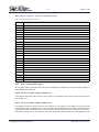
1
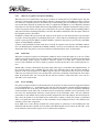
PCI to SpaceWire and 1553 Bridge
GR701A
User’s Manual
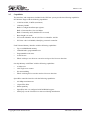
Features
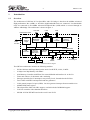
Description
• PCI bus Initiator and Target, 32-bit, 33 MHz
• EDAC protected interface to multiple 8-bit
SRAM memory, 16-bit I/O interface
• 16 kbyte EDAC protected On-chip Memory
• UARTs, Timers & Watchdog, GPIO port,
Interrupt controller, Status registers
• Multiple SpaceWire links with CRC, one link
with full RMAP support.
• Redundant Mil-Std-1553 BC / RT / MT
interface
• Redundant CAN 2.0 interface
• Up to 33 MHz system frequency
• 1.5V & 3.3V supply, 500 mW consumption
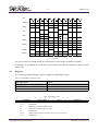
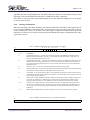
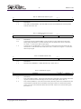
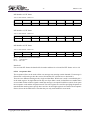
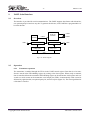
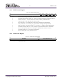
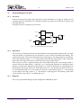
GR701A is a PCI to SpaceWire and Mil-Std1553 bridge. Its fault tolerant design is
implemented using the Actel RTAX FPGA
technology to enable total immunity to radiatio
effects.
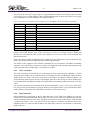
1553 A/B
Specification
• CQ352 baseline package
• Total Ionizing Dose up to 300 krad (Si,
functional)
• Single-Event Latch-Up Immunity (SEL) to
LETTH > 104 MeV-cm2/mg
• Immune to Single-Event Upsets (SEU) to
LETTH > 37 MeV-cm2/mg
LVDS
CAN
RTAX2000S FPGA
32-bit
PCI bus
Mil-Std-1553
BC/RT/MT
Interface
PCI
Initiator/
Target
CAN
2.0
Controller
On-Chip
Memory
with EDAC
32-bit AMBA AHB
32-bit AMBA APB
Memory
Controller
with EDAC
AHB
Controller
SpaceWire
Link
Interface
AHB/APB
Bridge
UART
Timers
RS232
WDOG
IrqCtrl
I/O Port
16-bit
SRAM
I/O
32-bit I/O port
Applications
The GR701A has been developed as a companion chip for space processors and systems with PCI
interfaces. This chip is available in an Actel RTAX2000S FPGA, which makes it ideally suited for
space and other high-rel applications. The chip is also available in an AX2000 FPGA for evaluation
and prototyping purposes.
Copyright Gaisler Research AB
June 2007, Version 1.0.0
2
1
Introduction
1.1
Overview
GR701A-UM
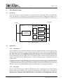
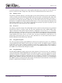
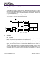
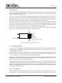
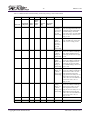
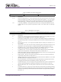
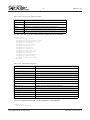
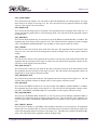
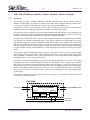
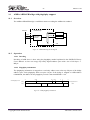
The architecture of GR701A PCI to SpaceWire and 1553 bridge is based on the AMBA Advanced
High-performance Bus (AHB), to which the high-bandwidth units are connected. Low-bandwidth
units are connected to the AMBA Advanced Peripheral Bus (APB) which is accessed through an
AHB to APB bridge. The architecture is shown in figure 1.
1553 A/B
LVDS
CAN
RTAX2000S FPGA
32-bit
PCI bus
Mil-Std-1553
BC/RT/MT
Interface
PCI
Initiator/
Target
CAN
2.0
Controller
On-Chip
Memory
with EDAC
32-bit AMBA AHB
32-bit AMBA APB
Memory
Controller
with EDAC
AHB
Controller
SpaceWire
Link
Interface
AHB/APB
Bridge
UART
Timers
RS232
WDOG
IrqCtrl
I/O Port
16-bit
SRAM
I/O
32-bit I/O port
Figure 1. Architectural block diagram
The GR701A architecture includes the following modules:
•
•
•
•
•
•
•
•
•
•
•
PCI bus Initiator and Target based on the Actel CorePCIF IP, 32-bit, 33 MHz
16 kbyte On-Chip Memory with EDAC
8-bit Memory Controller with EDAC for external SRAM and interface for 16-bit I/O
Timer unit with two 32-bit timers and a watchdog
Interrupt controller for 15 interrupts at two priority levels, forwarded to the PCI bus
Two UARTs with FIFO and separate baud rate generators
32-bit general purpose I/O port (GPIO). Can also generate interrupts from external devices
AMBA AHB status register
Three SpaceWire links with CRC support, one link includes full RMAP support
CAN-2.0 controller with redundant interfaces
Mil-Std-1553 BC/RT/MT based on the Actel Core1553 IP
Copyright Gaisler Research AB
June 2007, Version 1.0.0
3
2
Architecture
2.1
Cores
GR701A-UM
The architecture of the GR701A is based on cores from the GRLIB IP library. The vendor and device
identifiers for each core can be extracted from the plug & play information, as described in the user’s
manual. The used IP cores are listed in table 1.
Table 1. Used IP cores
2.2
Core
Function
Vendor
Device
AHBCTRL
AHB Arbiter & Decoder
0x01
-
APBCTRL
AHB/APB Bridge
0x01
0x006
PCIF
32-bit PCI interface
0x01
0x075
FTSRCTRL8
8-bit SRAM/16-bit IO Controller
0x01
0x056
FTAHBRAM
On-chip SRAM with EDAC
0x01
0x050
AHBSTAT
AHB failing address register
0x01
0x052
APBUART
8-bit UART with FIFO
0x01
0x00C
GPTIMER
Modular timer unit with watchdog
0x01
0x011
GRGPIO
General purpose I/O port
0x01
0x01A
GRSPW
SpaceWire link
0x01
0x01F
CAN_OC
CAN-2.0 interface
0x01
0x019
B1553BRM
MIL-STD-1553 BC/RT/BM
0x01
0x072
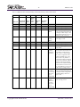
Interrupts
The GR701A uses the interrupt assignment listed in table 2. See the user’s manual for how and when
the interrupts are raised. All interrupts are handled by the interrupt controller and forwarded to the
PCI bus.
Table 2. Interrupt assignment
Core
Interrupt
AHBSTAT
1
APBUART 1
2
APBUART 2
3
CAN_OC
13
GPTIMER
8
GRSPW 0, 1, 2
10, 11, 12
B1553BRM
4
GRGPIO
1-15
Copyright Gaisler Research AB
Comment
Generated from external GPIO signals 1 to 15
June 2007, Version 1.0.0
4
2.3
GR701A-UM
Memory map
The memory map shown in table 3 is based on the AMBA AHB address space. Access to addresses
outside the ranges will return an AHB error response. The detailed register layout is defined in the
user manual.
Table 3. AMBA AHB address range
Core
Address range
Area
PCIF
0xE0000000 - 0xF0000000
PCI bus area
APBCTRL
0xFC000000 - 0xFC100000
APB bridge
FTSRCTRL8
0xFD000000 - 0xFE000000
SRAM area
0xFE000000 - 0xFF000000
I/O area
0xFFA00000 - 0xFFB00000
On-chip RAM
CAN_OC
0xFFFC0000 - 0xFFFC1000
Registers
B1553BRM
0xFFF00000 - 0xFFF01000
Registers
AHB plug&play
0xFFFFF000 - 0xFFFFFFFF
Registers
FTAHBRAM
The control registers of most on-chip peripherals are accessible via the AHB/APB bridge, which is
mapped at address 0xFC000000. The memory map shown in table 4 is based on the AMBA AHB
address space.
Table 4. APB address range
Core
Address range
FTSRCTRL8
0xFC000000 - 0xFC000100
APBUART1
0xFC000100 - 0xFC000200
AHBSTAT
0xFC000200 - 0xFC000300
GPTIMER
0xFC000300 - 0xFC000400
PCIF
0xFC000400 - 0xFC000500
FTAHBRAM
0xFC000500 - 0xFC000600
APBUART2
0xFC000700 - 0xFC000800
GRGPIO
0xFC000800 - 0xFC000900
GRSPW 0
0xFC000A00 - 0xFC000B00
GRSPW 1
0xFC000B00 - 0xFC000C00
GRSPW 2
0xFC000C00 - 0xFC000D00
APB plug&play
0xFC0FF000 - 0xFC100000
Copyright Gaisler Research AB
Comment
June 2007, Version 1.0.0
5
2.4
GR701A-UM
Plug & play information
The plug & play memory map and bus indexes for AMBA AHB masters are shown in table 5 and is
based on the AMBA AHB address space.
Table 5. Plug & play information for AHB masters
Core
Index
Function
Address range
PCIF
0
PCI interface
0xFFFFF000 - 0xFFFFF01F
GRSPW
1
SpaceWire link 0
0xFFFFF020 - 0xFFFFF03F
GRSPW
2
SpaceWire link 1
0xFFFFF040 - 0xFFFFF05F
GRSPW
3
SpaceWire link 2
0xFFFFF060 - 0xFFFFF07F
B1553BRM
4
MIL-STD-1553 BC/RT/BM
0xFFFFF080 - 0xFFFFF09F
The plug & play memory map and bus indexes for AMBA AHB slaves are shown in table 6 and is
based on the AMBA AHB address space.
Table 6. Plug & play information for AHB slaves
Core
Index
Function
Address range
FTSRCTRL8
0
8-bit SRAM/16-bit IO Controller
0xFFFFF800 - 0xFFFFF81F
APBCTRL
1
AHB/APB Bridge
0xFFFFF820 - 0xFFFFF83F
PCIF
2
PCI interface
0xFFFFF840 - 0xFFFFF85F
B1553BRM
3
MIL-STD-1553 BC/RT/BM
0xFFFFF860 - 0xFFFFF87F
CAN_OC
4
CAN-2.0 interface
0xFFFFF880 - 0xFFFFF89F
FTAHBRAM
5
On-chip SRAM with EDAC
0xFFFFF8A0 - 0xFFFFF8BF
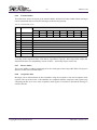
The plug & play memory map and bus indexes for AMBA AHB slaves are shown in table 7 and is
based on the AMBA AHB address space.
Table 7. Plug & play information for APB slaves
Core
Index
Function
Address range
FTSRCTRL8
0
8-bit SRAM/16-bit IO Controller
0xF00FF000 - 0xF00FF007
APBUART
1
8-bit UART with FIFO - 1
0xF00FF008 - 0xF00FF00F
AHBSTAT
2
AHB failing address register
0xF00FF010 - 0xF00FF017
GPTIMER
3
Modular timer unit with watchdog
0xF00FF018 - 0xF00FF01F
PCIF
4
PCI interface
0xF00FF020 - 0xF00FF027
FTAHBRAM
5
On-chip SRAM with EDAC
0xF00FF028 - 0xF00FF02F
GRGPIO
6
General purpose I/O port
0xF00FF030 - 0xF00FF037
APBUART
7
8-bit UART with FIFO - 2
0xF00FF038 - 0xF00FF03F
GRSPW
8
SpaceWire link 0
0xF00FF040 - 0xF00FF047
GRSPW
9
SpaceWire link 1
0xF00FF048 - 0xF00FF04F
GRSPW
10
SpaceWire link 2
0xF00FF050 - 0xF00FF057
Copyright Gaisler Research AB
June 2007, Version 1.0.0
6
2.5
GR701A-UM
Capabilities
The interfaces and components included in the GR701A system provide the following capabilities.
PCI Initiator/Target with the following capabilities:
•
32-bit bus width, 33 MHz (maximum)
•
3 Memory BARS
BAR 0: Configuration/Interrupt registers
BAR 1: Data transfers, Size: 64 Mbyte
BAR 5: Internally used (should not be accessed)
•
Burst length is 8 words
•
PCI vendor identifier: 0x1AC8, PCI device identifier: 0x0701
•
PCI class code is 0x028000, identifying a network controller
Fault Tolerant Memory Interface with the following capabilities:
•
Up to 16 MB SRAM memory
•
2 SRAM banks, programmable size
•
Programmable wait states
•
16-bit IO area
•
EDAC with up to two bit error correction and up to four bit error detection
On-chip Memory with EDAC with the following capabilities:
•
16 kbyte size
•
2 bit single error counter
•
No autoscrubbing
•
EDAC with single bit correction and two bit error detection
SpaceWire controller interface with the following capabilities:
•
100 Mbps maximum rate
•
3 SpaceWire links
•
DMA capability
•
SpaceWire link 2 is configured with full RMAP support
•
GPIO[3:0] sets the Clock divisor value used during initialization
Copyright Gaisler Research AB
June 2007, Version 1.0.0
7
GR701A-UM
Redundant MIL-STD-1553B bus controller interface with the following capabilities:
•
1 Mbps maximum rate
•
DMA capability
•
Bus Controller(BC), Remote Terminal(RT), and Monitor Terminal(MT) modes
•
24 MHz clock
GPIO interface with the following capabilities:
•
32 programmable input/output IO signals
•
GPIO[3:0] is used for SpaceWire configuration
Timers and Watchdog with the following capabilities:
•
8-bit prescaler
•
Two 32-bit timers. One timer can be used as watchdog timer
•
Watchdog reset value is set to 0x2FFFFF (24 sec @ 33 MHz system clock)
Copyright Gaisler Research AB
June 2007, Version 1.0.0
8
3
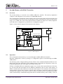
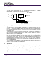
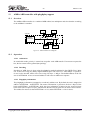
PCI Initiator/Target
3.1
Overview
GR701A-UM
This core provides a complete interface to an external PCI bus, with both initiator and target functions. The interface is based on the Actel CorePCIF IP and provides an AMBA bus backend. It also
provides a interrupt controller that forwards all interrupts generated on the AMBA bus to the PCI bus.
AMBA BUS
PCI BUS
PCI bridge
AMBA interface
AMBA AHB
Master
FIFO
CorePCIF
(PCI master/target)
AMBA AHB
Slave
Interrupt
ctrl
AMBA APB
Slave
Figure 2. Block diagram
3.2
Operation
3.2.1
PCI Initiator
The PCI initiator can be enabled and disabled in the PCI configuration space. The PCI master generates “Memory read multiple“ accesses on the PCI bus for burst read accesses to the AMBA backend.
For single read accesses to the AMBA backend, “Memory read“ accesses are generated on the PCI
bus. All write accesses to the AMBA backend generate “Memory write“ accesses on the PCI bus. The
most significant bits of the PCI address are set by mapping registers, while the least significant bits are
directly transferred from the AMBA backend. A separate mapping register is implemented for each
AMBA master.
To generate PCI accesses, the following steps must be executed. The master function must be enabled,
preferably by the PCI system host during the PCI configuration and the mapping register must be programmed with the most significant bits of the PCI address that should be accessed. After this, read
and write accesses to the AMBA backend will be transferred the corresponding PCI address.
3.2.2
PCI Target
The PCI target function can be enabled and disabled in the PCI configuration space. When enabled,
the PCI target accepts “Memory read“, “Memory read multiple“, and “Memory write“ commands for
data accesses. Access to the PCI configuration space is provided for “Configuration read“ and “Configuration write“ commands. When the PCI target is accessed (except for Configuration read/write),
Copyright Gaisler Research AB
June 2007, Version 1.0.0
9
GR701A-UM
the core transfers this access to the AMBA backend. The most significant bits of the address used by
the AMBA backend is controlled by a mapping register, while the least significant bits of the address
are directly transferred from the PCI access. A separate mapping register is implemented for PCI
BAR 1 - 4.
The following configuration steps are required for the PCI target to correctly respond to data accesses.
The target must be setup to accept memory accesses, preferably by the PCI system host during PCI
configuration. The mapping register must be programmed with the most significant bits of the AMBA
address. After this configuration, accesses to the PCI target interface are transferred to the AMBA
bus.
The PCI target interface provides three PCI memory bars: BAR 0 enables access to the configuration
registers; BAR 1 is used for data transfers; BAR 5 is used by the master function and should never be
accessed by any other master on the PCI bus.
3.2.3
Configuration
The core has configuration registers accessible via the AMBA APB interface and via the PCI BAR 0.
The PCI BAR to AMBA address mapping registers and the interrupt registers are accessible via the
PCI BAR 0. The interrupt registers must be setup to enable interrupt handling. The PCI to AMBA
address mapping registers must be setup to translate the PCI access into the correct AMBA access.
These mapping registers are also accessible via the AMBA APB interface. The AMBA to PCI address
mapping registers are accessible via the AMBA APB interface. These registers must be setup to translate the access to the AMBA AHB slave interface into the correct PCI address.
3.2.4
Byte access
Single byte accesses are supported by the interface. The byte is directly transferred between the two
buses (i.e. a write of the byte located at bit 7 - 0 on the AMBA bus is transferred to a write of the byte
located at bit 7 - 0 on the PCI bus). The core does not support the PCI byte-enables to be changed during burst accesses. The PCI byte-enable is only sampled for the first word in a burst.
3.2.5
Error response
The PCI target do not generate error responses. An PCI access that transfer into an AMBA access
with an invalid address is not generating an error response on the PCI bus.
The AMBA backend generate a two cycle error response in the following cases. When the AMBA
backend is accessed and the PCI master function is disabled, or when Master/Target abort is detected
by the PCI master. In the case of a Master/Target abort, the core automatically resets the error bits in
the PCI configuration space.
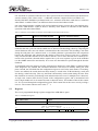
3.2.6
Interrupt controller
The interrupt controller monitors interrupt 1 - 15 provided by the AMBA system. Each interrupt can
be assigned to one of two levels (0 or 1) as programmed in the interrupt level register. Level 1 has
higher priority than level 0. The interrupt are prioritized within each level, with interrupt 15 having
the highest priority and interrupt 1 the lowest. The highest interrupt at level 1 will be forwarded to the
PCI bus. If no unmasked pending interrupt exist at level 1, then the highest interrupt at level 0 will be
forwarded. To determine which interrupt has occurred the interrupt status/ack register can be read. To
acknowledge the interrupt the interrupt status/ack register is written.
Copyright Gaisler Research AB
June 2007, Version 1.0.0
10
GR701A-UM
Priority
select
IRQ
Pending
Priority
encoder
4
15
APBI.PIRQ[15:1]
IRQ
Force
Interrupt
status register
and PCI interrupt
pin INTA
IRQ
mask
Figure 3. Block diagram
When an interrupt is acknowledged, the corresponding pending bit will automatically be cleared.
Interrupts may also be forced by setting a bit in the interrupt force register. In this case, the acknowledgement will clear the force bit rather than the pending bit. After reset, the interrupt mask register is
set to all zeros while the remaining control registers are undefined.
3.3
Registers
The core is programmed via registers mapped into the APB address space and into the PCI BAR 0.
Table 8. PCIF: APB registers
APB address offset
Register
0x00
PCI to AMBA mapping for PCI BAR 1
0x04
PCI to AMBA mapping for PCI BAR 2
0x08
PCI to AMBA mapping for PCI BAR 3
0x0C
PCI to AMBA mapping for PCI BAR 4
0x40 - 0x7C
AMBA master to PCI address mapping registers
The AMBA master to PCI mapping registers are all word aligned. Only the registers corresponding to
a master included in the system are implemented (i.e. if a system includes 8 masters, with master ID 0
to 7, the 8 first mapping registers are implemented).
Table 9. PCIF: PCI to AMBA mapping register
31
26
25
ABH address
0
RESERVED
31 : 26
MBS of the AMBA address
25 : 0
RESERVED
Copyright Gaisler Research AB
June 2007, Version 1.0.0
11
GR701A-UM
Table 10. PCIF: AMBA master to PCI mapping register
31
26
25
0
PCI address
RESERVED
31 : 26
MBS of the PCI address
25 : 0
RESERVED
Table 11. PCIF: PCI BAR 0 registers
PCI address offset
Register
0x00
PCI to AMBA mapping for PCI BAR 1
0x04
PCI to AMBA mapping for PCI BAR 2
0x08
PCI to AMBA mapping for PCI BAR 3
0x0C
PCI to AMBA mapping for PCI BAR 4
0x14
Interrupt level
0x18
Interrupt pending
0x1C
Interrupt force
0x20
Interrupt status/ack
0x24
Interrupt clear
0x28
Interrupt mask
Table 12. PCIF: Interrupt level register
31
16
15
RESERVED
1
0
1
0
IL[15:1]
31 : 16
RESERVED
15 : 1
Interrupt level n (IL[n]): Interrupt level for interrupt n
0
RESERVED
Table 13. PCIF: Interrupt pending register
31
16
15
RESERVED
31 : 16
RESERVED
15 : 1
Interrupt pending n (IP[n]): Interrupt pending for interrupt n
0
RESERVED
Copyright Gaisler Research AB
IP[15:1]
June 2007, Version 1.0.0
12
GR701A-UM
Table 14. PCIF: Interrupt force register
31
16
15
RESERVED
1
0
IF[15:1]
31 : 16
RESERVED
15 : 1
Interrupt force n (IF[n]): Force interrupt nr n
0
RESERVED
Table 15. PCIF: Interrupt status/ack register
31
4
RESERVED
31 : 4
RESERVED
3:0
Interrupt status
3
0
Status
Table 16. PCIF: Interrupt clear register
31
16
15
RESERVED
1
0
1
0
IC[15:1]
31 : 16
RESERVED
15 : 1
Interrupt clear n (IC[n]): Writing ‘1’ to IC[n] will clear interrupt n
0
RESERVED
Table 17. PCIF: Interrupt mask register
31
16
RESERVED
15
IM[15:1]
31 : 16
RESERVED
15 : 1
Interrupt mask n(IM[n]): If IM[n] = 0 the interrupt n is masked, otherwise it is enabled
0
RESERVED
Copyright Gaisler Research AB
June 2007, Version 1.0.0
13
Copyright Gaisler Research AB
GR701A-UM
June 2007, Version 1.0.0
14
4
Memory Interface with EDAC
4.1
Overview
GR701A-UM
The fault tolerant 8-bit SRAM/16-bit I/O memory interface uses a common 16-bit data bus to interface 8-bit SRAM and 16-bit I/O devices. It provides an Error Detection And Correction unit (EDAC),
correcting up to two errors and detecting up to four errors in a data byte. The EDAC eight checkbits
are stored in parallel with the 8-bit data in SRAM memory. Configuration of the memory controller
functions is performed through the APB bus interface.
A
AHB
SRO.RAMSN
SRO.OEN
SRO.WRITEN
D
A
CS
OE
WE
SRAM
CS
OE
WE
IO
D
MEMORY
CONTROLLER
SRO.IOSN
A
D
SRI.A[27:0]
SRI.D[15:0]
SRO.D[15:0]
AHB/APB
APB
Bridge
Figure 4. Block diagram
4.2
Operation
The controller is configured to decode two address ranges: SRAM and I/O area.One chip select is
decoded for the I/O area, while SRAM can have up to 8 chip select signals. The controller generates a
common write-enable signal (WRITEN) for both SRAM and I/O. The number of waitstates may be
separately configured for the two address ranges.
The configuration of the EDAC is done through a configuration register accessed from the APB bus.
During nominal operation, the EDAC checksum is generated and checked automatically. The 8-bit
input to the EDAC function is split into two 4-bit nibbles. A modified hamming(8,4,4) coding featuring a single error correction and double error detection is applied to each 4-bit nibble. This makes the
EDAC capable of correcting up to two errors and detecting up to four errors per 8-bit data. Single
errors (correctable errors) are corrected without generating any indication of this condition in the bus
response. If a multiple error (uncorrectable errors) is detected, a two cycle error response is given on
the AHB bus.
The EDAC function can only be enabled for SRAM area accesses. If a 16-bit or 32-bit bus access is
performed, the memory controller calculates the EDAC checksum for each byte read from the mem-
Copyright Gaisler Research AB
June 2007, Version 1.0.0
15
GR701A-UM
ory but the indication of single error is only signaled when the access is done. (I.e. if more than one
byte in a 32-bit access has a single error, only one error is indicated for the hole 32-bit access.)
4.2.1
Memory access
The memory controller supports 32/16/8-bit single accesses and 32-bit burst accesses to the SRAM. A
32-bit or a 16-bit access is performed as multiple 8-bit accesses on the 16-bit memory bus, where data
is transferred on data lines 8 to 15 (Data[15:8]). The eight checkbits generated/used by the EDAC is
transferred on the eight first data lines (Data[7:0]). For 32-bit and 16-bit accesses, the bytes read from
the memory is arranged according to the big-endian order (i.e. for a 32-bit read access, the bytes read
from memory address A, A+1, A+2, and A+3 correspond to the bit[31:24], bit[23:16], bit[15:8], and
bit[7:0] in the 32-bit word transferred to the AMBA bus.
4.2.2
I/O access
The memory controller accepts 32/16/8-bit single accesses to the I/O area, but the access generated
towards the I/O device is always 16-bit. The two least significant bits of the AMBA address (byte
address) determine which half word that should be transferred to the I/O device. (i.e. If the byte
address is 0 and it is a 32-bit access, bits 16 to 31 on the AHB bus is transferred on the 16-bit memory
bus. If the byte address is 2 and it is a 16-bit access, bit 0 to 15 on the AHB bus is transferred on the
16-bit memory bus.) If the access is an 8-bit access, the data is transferred on data lines 8 to 15
(Data[15:8]) on the memory bus. In case of a write, data lines 0 to 7 is also written to the I/O device
but these data lines do not transfer any valid data.
4.2.3
Using Bus Exception
The active low Bus Exception signal (BEXCN) can be used to signal access errors. It is enabled by
setting the BEXCEN bit in MCFG1 and is only active for the I/O area. The BEXCN signal is sampled
on the same cycle as data is written to memory or read data is sampled. When a bus exception is
detected an error response will be generated for the access. One additional latency cycle is added to
the AMBA access when the Bus Exception is enable.
4.2.4
Using Bus Ready
The Bus Ready (BRDYN) signal can be used to add waitstates to I/O-area accesses. It is enabled by
setting the Bus Ready Enable (BRDYEN) bit in the MCFG1 register. An access will have at least the
amount of waitstates set through the register, but will be further stretched until BRDYN is asserted.
Additional waitstates can thus be inserted after the pre-set number of waitstates by deasserting the
BRDYN signal. BRDYN should be asserted in the cycle preceding the last one. It is recommended
that BRDY remains asserted until the IOSN signal is de-asserted, to ensure that the access has been
properly completed and avoiding the system to stall.
Copyright Gaisler Research AB
June 2007, Version 1.0.0
16
lead-in
wait
data
GR701A-UM
data
clk
address
A1
iosn
oen
data
D1
brdyn
first
sample
Figure 5. I/O READ cycle, programmed with 1 wait state, and with an extra data cycle added with BRDYN.
4.3
SRAM/IO waveforms
The internal and external waveforms of the interface are presented in the figures below.
clk
address
A0
A1
A2
A3
A4
A5
A6
A7
ramsn
oen
data
haddr
htrans
B3
B2
A0
A4
10
11
B1
B0
B7
B6
B5
B4
A8
00
hready
hrdata
D0
D1
Figure 6. 32-bit SRAM sequential read accesses with 0
wait-states and EDAC enabled.
Copyright Gaisler Research AB
June 2007, Version 1.0.0
17
GR701A-UM
clk
address
A0
A1
A2
A3
A4
ramsn
writen
data
haddr
htrans
B3
B2
B1
B0
A0
A4
A8
10
11
00
B4
hready
hwdata
D1
D0
Figure 7. 32-bit SRAM sequential writeaccess with 0 waitstates and EDAC enabled.
clk
address
A0
A1
ramsn
writen
data
haddr
htrans
B3
B2
A0
A1
A2
10
11
00
hready
hwdata
D0
D1
Figure 8. 8-bit SRAM non-sequential write access with 0
wait-states and EDAC enabled.
Copyright Gaisler Research AB
June 2007, Version 1.0.0
18
GR701A-UM
clk
address
A0
A1
ramsn
oen
data
B3
haddr
A1
A0
htrans
B2
A2
10
10
00
hready
hrdata
D[31:24]
D[23:16]
Figure 9. 8-bit SRAM non-sequential read access with 0
wait-states and EDAC enabled.
On a read access, data is sampled one clock cycle before HREADY is asserted.
clk
address
A0
iosn
writen
data
haddr
htrans
H1
A0
A1
10
00
hready
hwdata
D[31:16]
Figure 10. 16-bit I/O non-sequential write access with 0
wait-states.
Copyright Gaisler Research AB
June 2007, Version 1.0.0
19
GR701A-UM
clk
address
A4
A2
ramsn
oen
data
H1
haddr
A4
A2
htrans
H3
00
10
10
hready
hrdata
D[15:0]
D[31:16]
Figure 11. 16-bit I/O non-sequential read access with 0
wait-states.
I/O write accesses are extended with one extra latency cycle if the bus exception is enabled.
If waitstates are configured, one extra data cycle will be inserted for each waitstate in both read and
write cycles.
4.4
Registers
The core is programmed through registers mapped into APB address space.
Table 18. FT SRAM/IO controller registers
APB Address offset
Register
0x0
Memory configuration register 1
0x4
Memory configuration register 2
0x8
Memory configuration register 3
Table 19. MCFG1 register
31
27
RESERVED
26
25
BRDY
BEXC
24
23
20
IOWS
31 : 27
RESERVED
26
BRDYEN: Enables the BRDYN signal.
25
BEXCEN: Enables the BEXCN signal.
24
RESERVED
23 : 20
IOWS: Sets the number of waitstates for accesses to the IO area.
19 : 0
RESERVED
Copyright Gaisler Research AB
19
0
RESERVED
June 2007, Version 1.0.0
20
GR701A-UM
Table 20. MCFG2 register
31
13
RESERVED
12
9
8
2
RAMBSZ
1
RESERVED
0
RAMWS
31 : 12
RESERVED
12 : 9
RAMBSZ: Sets the SRAM bank size.
8:2
RESERVED
1:0
RAMWS: Sets the number of waitstates for accesses to the RAM area.
Table 21. MCFG3 register
31
12
RESERVED
11
10
9
WB
RB
SEN
8
7
0
TCB
31 : 12
RESERVED
11
WB: Write bypass. If set, the TCB field will be used as checkbits in all write operations.
10
RB: Read bypass. If set, checkbits read from memory in all read operations will be stored in the TCB
field.
9
SEN: SRAM EDAC enable. If set, EDAC will be active for the SRAM area.
8
RESERVED
7:0
TCB: Used as checkbits in write operations when WB is one and checkbits from read operations are
stored here when RB is one.
Copyright Gaisler Research AB
June 2007, Version 1.0.0
21
GR701A-UM
5
On-chip Memory with EDAC Protection
5.1
Overview
The on-chip memory is accessed via an AMBA AHB slave interface. The memory implements
16 kbytes of data. Registers are accessed via an AMB APB interface.
The on-chip memory implements volatile memory that is protected by means of Error Detection And
Correction (EDAC). One error can be corrected and two errors can be detected, which is performed by
using a (32, 7) BCH code. Some of the optional features available are single error counter, diagnostic
reads and writes. Configuration is performed via a configuration register.
Figure 12 shows a block diagram of the internals of the memory.
AHB Bus
AHB Slave
Interface
FTAHBRAM
data
Mux
AHB/APB
Bridge
error Configuration Register
Mux
Encoding
Config bits
TCB
cb
APB Bus
Decoding
Mux
data
cb
Syncram
Figure 12. Block diagram
5.2
Operation
The on-chip fault tolerant memory is accessed through an AMBA AHB slave interface.
Run-time configuration is done by writing to a configuration register accessed through an AMBA
APB interface.
The following can be configured during run-time: EDAC can be enabled and disabled. When it is disabled, reads and writes will behave as the standard memory. Read and write diagnostics can be controlled through separate bits. The single error counter can be reset.
If EDAC is disabled (EN bit in configuration register set to 0) write data is passed directly to the memory area and read data will appear on the AHB bus immediately after it arrives from memory. If
EDAC is enabled write data is passed to an encoder which outputs a 7-bit checksum. The checksum is
stored together with the data in memory and the whole operation is performed without any added
waitstates. This applies to word stores (32-bit). If a byte or halfword store is performed, the whole
word to which the byte or halfword belongs must first be read from memory (read - modify - write). A
Copyright Gaisler Research AB
June 2007, Version 1.0.0
22
GR701A-UM
new checksum is calculated when the new data is placed in the word and both data and checksum are
stored in memory. This is done with 1 - 2 additional waitstates compared to the non EDAC case.
Reads with EDAC disabled are performed with 0 or 1 waitstates while there could also be 2 waitstates
when EDAC is enabled. There is no difference between word and subword reads.
One extra initial waitstate is added to all read and subword writes accesses due to the pipeline structure of the AHB interface. Table 22 shows a summary of the number of waitstates for the different
operations with and without EDAC.
Table 22. Summary of the number of waitstates for the different operations for the memory.
Operation
Waitstates with EDAC Disabled
Waitstates with EDAC Enabled
Read
0-2
0-3
Word write
0
0
Subword write
0
1-3
When EDAC is used, the data is decoded the first cycle after it arrives from the memory and appears
on the bus the next cycle if no uncorrectable error is detected. The decoding is done by comparing the
stored checksum with a new one which is calculated from the stored data. This decoding is also done
during the read phase for a subword write. A so-called syndrome is generated from the comparison
between the checksum and it determines the number of errors that occurred. One error is automatically corrected and this situation is not visible on the bus. Two or more detected errors cannot be corrected so the operation is aborted and the required two cycle error response is given on the AHB bus
(see the AMBA manual for more details). If no errors are detected data is passed through the decoder
unaltered.
As mentioned earlier the memory provides read and write diagnostics when EDAC is enabled. When
write diagnostics are enabled, the calculated checksum is not stored in memory during the write
phase. Instead, the TCB field from the configuration register is used. In the same manner, if read diagnostics are enabled, the stored checksum from memory is stored in the TCB field during a read (and
also during a subword write). This way, the EDAC functionality can be tested during run-time. Note
that checkbits are stored in TCB during reads and subword writes even if a multiple error is detected.
A single error counter (SEC) field is present in the configuration register, and is incremented each
time a single databit error is encountered (reads or subword writes). The number of bits of this counter
is 2. It is accessed through the configuration register. Each counter bit can be reset to zero by writing a
one to it. The counter saturates at the value 22 - 1.
5.3
Registers
The core is programmed through registers mapped into APB address space.
Table 23. FTAHBRAM registers
APB Address offset
Register
0x0
Configuration Register
Table 24. Configuration Register
31
13+2
12+2
13 12
SEC
Copyright Gaisler Research AB
10
9
8
7
MEMSIZE WB RB EN
6
0
TCB
June 2007, Version 1.0.0
23
GR701A-UM
12+2: 13
Table 24. Configuration Register
Single error counter (SEC): Incremented each time a single error is corrected (includes errors on
checkbits). Each bit can be set to zero by writing a one to it.
12:
Log2 of the current memory size
10
9
Write Bypass (WB): When set, the TCB field is stored as check bits when a write is performed to the
memory.
8
Read Bypass (RB) : When set during a read or subword write, the check bits loaded from memory
are stored in the TCB field.
7
EDAC Enable (EB): When set, the EDAC is used otherwise it is bypassed during read and write
operations.
6: 0
Test Check Bits (TCB) : Used as checkbits when the WB bit is set during writes and loaded with the
check bits during a read operation when the RB bit is set.
Any unused most significant bits are reserved. Always read as ‘000...0’.
All fields except TCB are initialized at reset. The EDAC is initally disabled (EN = 0), which also applies to diagnostics fiels (RB and WB are zero).
When available, the single error counter (SEC) field is cleared to zero.
Copyright Gaisler Research AB
June 2007, Version 1.0.0
24
6
SpaceWire with Interface RMAP support
6.1
Overview
GR701A-UM
The SpaceWire core provides an interface between the AHB bus and a SpaceWire network. It implements the SpaceWire standard (ECSS-E-50-12A) with the protocol identification extension (ECSS-E50-11). The optional Remote Memory Access Protocol (RMAP) command handler implements the
ECSS standard (ECSS-E-50-11).
The SpaceWire interface is configured through a set of registers accessed through an APB interface.
Data is transferred through DMA channels using an AHB master interface.
The core can also be configured to have either one or two ports.
TXCLK
D(1:0)
TRANSMITTER
S(1:0)
LINKINTERFACE
FSM
SEND
FSM
TRANSMITTER
FSM
RMAP
TRANSMITTER
TRANSMITTER
DMA ENGINE
AHB
MASTER INTERFACE
RECEIVER
DMA ENGINE
D0
S0
RXCLK RECEIVER0
RXCLK
RECOVERY
RMAP
RECEIVER
RECEIVER
AHB FIFO
RXCLK RECEIVER1
RXCLK
RECOVERY
N-CHAR
FIFO
RECEIVER DATA
PARALLELIZATION
REGISTERS
APB
INTERFACE
D1
S1
Figure 13. Block diagram
6.2
Operation
6.2.1
Overview
The GRSPW can be split into three main parts: the link interface, the AMBA interface and the RMAP
handler. A block diagram of the internal structure can be found in figure 13.
The link interface consists of the receiver, transmitter and the link interface FSM. They handle communication on the SpaceWire network. The AMBA interface consists of the DMA engines, the AHB
master interface and the APB interface. The link interface provides FIFO interfaces to the DMA
engines. These FIFOs are used to transfer N-Chars between the AMBA and SpaceWire domains during reception and transmission.
The RMAP handler handles incoming packets which are determined to be RMAP commands instead
of the receiver DMA engine. The RMAP command is decoded and if it is valid, the operation is performed on the AHB bus. If a reply was requested it is automatically transmitted back to the source by
the RMAP transmitter.
Copyright Gaisler Research AB
June 2007, Version 1.0.0
25
6.2.2
GR701A-UM
Protocol support
The GRSPW only accepts packets with a destination address corresponding to the one set in the node
address register. Packets with address mismatch will be silently discarded (except in promiscuous
mode which is covered in section 6.4.10). The node address register is initialized to the default
address 254 during reset. It can then be changed to some other value by writing to the register.
The GRSPW also requires that the byte following the destination address is a protocol identifier as
specified in part 2 of the SpaceWire standard. It is used to determine to which DMA-channel a packet
is destined. Currently only one channel is available to which all packets (except RMAP commands)
are stored but the GRSPW is prepared to be easily expandable with more DMA channels. Figure 14
shows the packet type expected by the GRSPW.
RMAP (Protocol ID = 0x01) commands are handled separately from other packets if the hardware
RMAP handler is enabled. When enabled, all RMAP commands are processed, executed and replied
in hardware. All RMAP replies received are still stored to the DMA channel. If the RMAP handler is
disabled, all packets are stored to the DMA channel.
All packets arriving with the extended protocol ID (0x00) are stored to the DMA channel. This means
that the hardware RMAP command handler will not work if the incoming RMAP packets use the
extended protocol ID. Note also that packets with the reserved extended protocol identifier (ID =
0x000000) are not ignored by the GRSPW. It is up to the client receiving the packets to ignore them.
When transmitting packets, the address and protocol-ID fields must be included in the buffers from
where data is fetched. They are not automatically added by the GRSPW.
Figure 14 shows a packet with a normal protocol identifier. The GRSPW also allows reception and
transmission with extended protocol identifiers but then the hardware RMAP and RMAP CRC calculations will not work.
Addr ProtID D0
D1
D2
D3
..
Dn-2 Dn-1 EOP
Figure 14. The SpaceWire packet with protocol ID that is expected by the GRSPW.
6.3
Link interface
The link interface handles the communication on the SpaceWire network and consists of a transmitter,
receiver, a FSM and FIFO interfaces. An overview of the architecture is found in figure 13.
6.3.1
Link interface FSM
The FSM controls the link interface (a more detailed description is found in the SpaceWire standard).
The low-level protocol handling (the signal and character level of the SpaceWire standard) is handled
by the transmitter and receiver while the FSM in the host domain handles the exchange level.
The link interface FSM is controlled through the control register. The link can be disabled through the
link disable bit, which depending on the current state, either prevents the link interface from reaching
the started state or forces it to the error-reset state. When the link is not disabled, the link interface
FSM is allowed to enter the started state when either the link start bit is set or when a NULL character
has been received and the autostart bit is set.
Copyright Gaisler Research AB
June 2007, Version 1.0.0
26
GR701A-UM
The current state of the link interface determines which type of characters are allowed to be transmitted which together with the requests made from the host interfaces determine what character will be
sent.
Time-codes are sent when the FSM is in the run-state and a request is made through the time-interface
(described in section 6.3.5).
When the link interface is in the connecting- or run-state it is allowed to send FCTs. FCTs are sent
automatically by the link interface when possible. This is done based on the maximum value of 56 for
the outstanding credit counter and the currently free space in the receiver N-Char FIFO. FCTs are sent
as long as the outstanding counter is less than or equal to 48 and there are at least 8 more empty FIFO
entries than the counter value.
N-Chars are sent in the run-state when they are available from the transmitter FIFO and there are credits available. NULLs are sent when no other character transmission is requested or the FSM is in a
state where no other transmissions are allowed.
The credit counter (incoming credits) is automatically increased when FCTs are received and
decreased when N-Chars are transmitted. Received N-Chars are stored to the receiver N-Char FIFO
for further handling by the DMA interface. Received Time-codes are handled by the time-interface.
6.3.2
Transmitter
The state of the FSM, credit counters, requests from the time-interface and requests from the DMAinterface are used to decide the next character to be transmitted. The type of character and the character itself (for N-Chars and Time-codes) to be transmitted are presented to the low-level transmitter
which is located in a separate clock-domain.
This is done because one usually wants to run the SpaceWire link on a different frequency than the
host system clock. The GRSPW has a separate clock input which is used to generate the transmitter
clock. Since the transmitter often runs on high frequency clocks (> 100 MHz) as much logic as possible has been placed in the system clock domain to minimize power consumption and timing issues.
The transmitter logic in the host clock domain decides what character to send next and sets the proper
control signal and presents any needed character to the low-level transmitter as shown in figure 15.
The transmitter sends the requested characters and generates parity and control bits as needed. If no
requests are made from the host domain, NULLs are sent as long as the transmitter is enabled. Most
of the signal and character levels of the SpaceWire standard is handled in the transmitter. External
LVDS drivers are needed for the data and strobe signals.
D
S
Transmitter
Transmitter Clock Domain
Send Time-code
Send FCT
Send NChar
Time-code[7:0]
NChar[8:0]
Host Clock Domain
Figure 15. Schematic of the link interface transmitter.
A transmission FSM reads N-Chars for transmission from the transmitter FIFO. It is given packet
lengths from the DMA interface and appends EOPs/EEPs and RMAP CRC values if requested. When
it is finished with a packet the DMA interface is notified and a new packet length value is given.
Copyright Gaisler Research AB
June 2007, Version 1.0.0
27
6.3.3
GR701A-UM
Receiver
The receiver detects connections from other nodes and receives characters as a bit stream on the data
and strobe signals. It is also located in a separate clock domain which runs on a clock generated from
the received data and strobe signals.
The receiver is activated as soon as the link interface leaves the error reset state. Then after a NULL is
received it can start receiving any characters. It detects parity, escape and credit errors which causes
the link interface to enter the error reset state. Disconnections are handled in the link interface part in
the system clock domain because no receiver clock is available when disconnected.
Received Characters are flagged to the host domain and the data is presented in parallel form. The
interface to the host domain is shown in figure 16. L-Chars are the handled automatically by the host
domain link interface part while all N-Chars are stored in the receiver FIFO for further handling. If
two or more consecutive EOPs/EEPs are received all but the first are discarded.
There are no signals going directly from the transmitter clock domain to the receiver clock domain
and vice versa. All the synchronization is done to the system clock.
D
Receiver
S
Receiver Clock Domain
Got Time-code
Got FCT
Got EOP
Got EEP
Got NChar
Time-code[7:0]
NChar[7:0]
Host Clock Domain
Figure 16. Schematic of the link interface receiver.
6.3.4
Dual port support
The core can be configured to include an additional SpaceWire port. In this case the transmitter drives
an additional pair of data/strobe output signals and one extra receiver is added to handle a second pair
of data/strobe input signals.
One of the ports is set as active (how the active port is selected is explained below) and the transmitter
drives the data/strobe signals of the active port with the actual output values as explained in section
6.3.2. The inactive port is driven with zero on both data and strobe.
Both receivers will always be active but only the active port’s interface signals (see figure 16) will be
propagated to the link interface FSM. Each time the active port is changed, the link will be reset so
that the new link is started in a controlled manner.
When the noportforce register is zero the portsel register bit selects the active link and when set to one
it is determined by the current link activity. In the latter mode the port is changed when no activity is
seen on the currently active link while there is activity on the deselected receive port. Activity is
defined as a detected null. This definition is selected so that glitches (e.g. port unconnected) do not
cause unwanted port switches.
6.3.5
Time interface
The time interface is used for sending Time-codes over the SpaceWire network and consists of a timecounter register, time-ctrl register, tick-in signal, tick-out signal, tick-in register field and a tick-out
Copyright Gaisler Research AB
June 2007, Version 1.0.0
28
GR701A-UM
register field. There are also two control register bits which enable the time receiver and transmitter
respectively.
Each Time-code sent from the grspw is a concatenation of the time-ctrl and the time-counter register.
There is a timetxen bit which is used to enable Time-code transmissions. It is not possible to send
time-codes if this bit is zero.
Received Time-codes are stored to the same time-ctrl and time-counter registers which are used for
transmission. The timerxen bit in the control register is used for enabling time-code reception. No
time-codes will be received if this bit is zero.
The two enable bits are used for insuring that a node will not (accidentally) both transmit and receive
time-codes which violates the SpaceWire standard. It also insures that a the master sending timecodes on a network will not have its time-counter overwritten if another (faulty) node starts sending
time-codes.
The time-counter register is set to 0 after reset and is incremented each time the tick-in signal is
asserted for one clock-period and the timetxen bit is set. This also causes the link interface to send the
new value on the network. Tick-in can be generated either by writing a one to the register field or by
asserting the tick-in signal. A Tick-in should not be generated too often since if the time-code after the
previous Tick-in has not been sent the register will not be incremented and no new value will be sent.
The tick-in field is automatically cleared when the value has been sent and thus no new ticks should
be generated until this field is zero. If the tick-in signal is used there should be at least 4 system-clock
and 25 transmit-clock cycles between each assertion.
A tick-out is generated each time a valid time-code is received and the timerxen bit is set. When the
tick-out is generated the tick-out signal will be asserted one clock-cycle and the tick-out register field
is asserted until it is cleared by writing a one to it.
The current time counter value can be read from the time register. It is updated each time a Time-code
is received and the timerxen bit is set. The same register is used for transmissions and can also be
written directly from the APB interface.
The control bits of the Time-code are always stored to the time-ctrl register when a Time-code is
received whose time-count is one more than the nodes current time-counter register. The time-ctrl register can be read through the APB interface. The same register is used during time-code transmissions.
It is possible to have both the time-transmission and reception functions enabled at the same time.
6.4
Receiver DMA engine
The receiver DMA engine handles reception of data from the SpaceWire network to different DMA
channels. Currently there is only one receive DMA channel available but the GRSPW has been written so that additional channels can be easily added if needed.
6.4.1
Basic functionality
The receiver DMA engine reads N-Chars from the N-Char FIFO and stores them to a DMA channel.
Reception is based on descriptors located in a consecutive area in memory that hold pointers to buffers where packets should be stored. When a packet arrives at the GRSPW it reads a descriptor from
memory and stores the packet to the memory area pointed to by the descriptor. Then it stores status to
the same descriptor and increments the descriptor pointer to the next one.
Copyright Gaisler Research AB
June 2007, Version 1.0.0
29
6.4.2
GR701A-UM
Setting up the GRSPW for reception
A few registers need to be initialized before reception can take place. First the link interface need to
be put in the run state before any data can be sent. The DMA channel has a maximum length register
which sets the maximum size of packet that can be received to this channel. Larger packets are truncated and the excessive part is spilled. If this happens an indication will be given in the status field of
the descriptor. The minimum value for the receiver maximum length field is 4 and the value can only
be incremented in steps of four bytes. If the maximum length is set to zero the receiver will not function correctly.
The node address register needs to be set to hold the address of this SpaceWire node. Packets received
with the incorrect address are discarded. Finally, the descriptor table and control register must be initialized. This will be described in the two following sections.
6.4.3
Setting up the descriptor table address
The GRSPW reads descriptors from a area in memory pointed to by the receiver descriptor table
address register. The register consists of a base address and a descriptor selector. The base address
points to the beginning of the area and must start on a 1 kbytes aligned address. It is also limited to be
1 kbytes in size which means the maximum number of descriptors is 128.
The descriptor selector points to individual descriptors and is increased by 1 when a descriptor has
been used. When the selector reaches the upper limit of the area it wraps to the beginning automatically. It can also be set to wrap automatically by setting a bit in the descriptors. The idea is that the
selector should be initialized to 0 (start of the descriptor area) but it can also be written with another 8
bytes aligned value to start somewhere in the middle of the area. It will still wrap to the beginning of
the area.
If one wants to use a new descriptor table the receiver enable bit has to be cleared first. When the rxactive bit for the channel is cleared it is safe to update the descriptor table register. When this is finished
and descriptors are enabled the receiver enable bit can be set again.
6.4.4
Enabling descriptors
As mentioned earlier one or more descriptors must be enabled before reception can take place. Each
descriptor is 8 byte in size and the layout can be found in the tables below. The descriptors should be
written to the memory area pointed to by the receiver descriptor table address register. When new
descriptors are added they must always be placed after the previous one written to the area. Otherwise
they will not be noticed.
A descriptor is enabled by setting the address pointer to point at a location where data can be stored
and then setting the enable bit. The WR bit can be set to cause the selector to be set to zero when
reception has finished to this descriptor. IE should be set if an interrupt is wanted when the reception
has finished. The DMA control register interrupt enable bit must also be set for this to happen.
The descriptor packet address should be word aligned. All accesses on the bus are word accesses so
complete words will always be overwritten regardless of whether all 32-bit contain received data.
Also if the packet does not end on a word boundary the complete word containing the last data byte
will be overwritten.
Table 25. GRSPW receive descriptor word 0 (address offset 0x0)
31 30 29 28 27 26 25 24
TR DC HC EP IE WR EN
Copyright Gaisler Research AB
0
PACKETLENGTH
June 2007, Version 1.0.0
30
GR701A-UM
Table 25. GRSPW receive descriptor word 0 (address offset 0x0)
31
Truncated (TR) - Packet was truncated due to maximum length violation.
30
Data CRC (DC) - 1 if a CRC error was detected for the data and 0 otherwise.
29
Header CRC (HC) - 1 if a CRC error was detected for the header and 0 otherwise.
28
EEP termination (EP) - This packet ended with an Error End of Packet character.
27
Interrupt enable (IE) - If set, an interrupt will be generated when a packet has been received if the
receive interrupt enable bit in the DMA channel control register is set.
26
Wrap (WR) - If set, the next descriptor used by the GRSPW will be the first one in the descriptor
table (at the base address). Otherwise the descriptor pointer will be increased with 0x8 to use the
descriptor at the next higher memory location. The descriptor table is limited to 1 kbytes in size and
the pointer will be automatically wrap back to the base address when it reaches the 1 kbytes boundary.
25
Enable (EN) - Set to one to activate this descriptor. This means that the descriptor contains valid control values and the memory area pointed to by the packet address field can be used to store a packet.
24: 0
Packet length (PACKETLENGTH) - The number of bytes received to this buffer. Only valid after
EN has been set to 0 by the GRSPW.
Table 26. GRSPW receive descriptor word 1 (address offset 0x4)
31
0
PACKETADDRESS
31: 0
6.4.5
Packet address (PACKETADDRESS) - The address pointing at the buffer which will be used to store
the received packet.
Setting up the DMA control register
To final step to receive packets is to set the control register in the following steps: The receiver must
be enabled by setting the rxen bit in the DMA control register. This can be done anytime and before
this bit is set nothing will happen. The rxdescav bit in the DMA control register is then set to indicate
that there are new active descriptors. This must always be done after the descriptors have been
enabled or the GRSPW might not notice the new descriptors. More descriptors can be activated when
reception has already started by enabling the descriptors and writing the rxdescav bit. When these bits
are set reception will start immediately when data is arriving.
6.4.6
The effect to the control bits during reception
When the receiver is disabled all packets going to the DMA-channel are discarded. If the receiver is
enabled the next state is entered where the rxdescav bit is checked. This bit indicates whether there are
active descriptors or not and should be set by the external application using the DMA channel each
time descriptors are enabled as mentioned above. If the rxdescav bit is ‘0’ and the nospill bit is ‘0’ the
packets will be discarded. If nospill is one the grspw waits until rxdescav is set.
When rxdescav is set the next descriptor is read and if enabled the packet is received to the buffer. If
the read descriptor is not enabled, rxdescav is set to ‘0’ and the packet is spilled depending on the
value of nospill.
The receiver can be disabled at any time and will cause all packets received afterwards to be discarded. If a packet is currently received when the receiver is disabled the reception will still be finished. The rxdescav bit can also be cleared at any time. It will not affect any ongoing receptions but no
more descriptors will be read until it is set again. Rxdescav is also cleared by the GRSPW when it
reads a disabled descriptor.
Copyright Gaisler Research AB
June 2007, Version 1.0.0
31
6.4.7
GR701A-UM
Address recognition and packet handling
When the receiver N-Char FIFO is not empty, N-Chars are read by the receiver DMA engine. The first
character is interpreted as the logical address which is compared to the node address register. If it does
not match, the complete packet is discarded (up to and including the next EOP/EEP). Otherwise the
next action taken depends on whether the node is configured with RMAP or not. If RMAP is disabled
all packets are stored to the DMA channel and depending on the conditions mentioned in the previous
section, the packet will be received or not. If the packet is received complete packet including address
and protocol ID but excluding EOP/EEP is stored to the address indicated in the descriptor, otherwise
the complete packet is discarded.
If RMAP is enabled the protocol ID and 3rd byte in the packet is first checked before any decisions
are made. If incoming packet is an RMAP packet (ID = 0x01) and the command type field is 01b the
packet is processed by the RMAP command handler. Otherwise the packet is processed by the DMA
engine as when RMAP is disabled.
At least 2 non EOP/EEP N-Chars needs to be received for a packet to be stored to the DMA channel.
If it is an RMAP packet with hardware RMAP enabled 3 N-Chars are needed since the command byte
determines where the packet is processed. Packets smaller than these sizes are discarded.
6.4.8
Status bits
When the reception of a packet is finished the enable bit in the current descriptor is set to zero. When
enable is zero, the status bits are also valid and the number of received bytes is indicated in the length
field. The DMA control register contains a status bit which is set each time a packet has been
received. The GRSPW can also be made to generate an interrupt for this event as mentioned in section.
RMAP CRC is always checked for all packets when CRC logic is included in the implementation . If
the received packet is not of RMAP type the CRC error indication bits in the descriptor should be
ignored. If the received packet is of RMAP type the bits are valid and the HC bit is set if a header
CRC error was detected. In this case, the data CRC will not be calculated at all and the DC bit is undefined. If the header CRC was correct the DC bit will also contain a valid value and is set to one if a
data CRC error was detected.
6.4.9
Error handling
If a packet reception needs to be aborted because of congestion on the network, the suggested solution
is to set link disable to ‘1’. Unfortunately, this will also cause the packet currently being transmitted to
be truncated but this is the only safe solution since packet reception is a passive operation depending
on the transmitter at the other end. A channel reset bit could be provided but is not a satisfactory solution since the untransmitted characters would still be in the transmitter node. The next character
(somewhere in the middle of the packet) would be interpreted as the node address which would probably cause the packet to be discarded but not with 100% certainty. Usually this action is performed
when a reception has stuck because of the transmitter not providing more data. The channel reset
would not resolve this congestion.
If an AHB error occurs during reception the current packet is spilled up to and including the next
EEP/EOP and then the currently active channel is disabled and the receiver enters the idle state. A bit
in the channels control/status register is set to indicate this condition.
Copyright Gaisler Research AB
June 2007, Version 1.0.0
32
GR701A-UM
6.4.10 Promiscuous mode
The GRSPW supports a promiscuous mode where all the data received is stored to the DMA channel
regardless of the node address and possible early EOPs/EEPs. This means that all non-eop/eep NChars received will be stored to the DMA channel. The rxmaxlength register is still checked and
packets exceeding this size will be truncated.
If the RMAP handler is present, RMAP commands will still be handled by it when promiscuous mode
is enabled if the rmapen bit is set. If it is cleared, RMAP commands will also be stored to the DMA
channel.
6.5
Transmitter DMA engine
The transmitter DMA engine handles transmission of data from the DMA channel to the SpaceWire
network. Currently there is only one DMA channel available but the GRSPW has been written so that
additional DMA channels can be easily added if needed.
6.5.1
Basic functionality
The transmit DMA engine reads data from the AHB bus and stores them in the transmitter FIFO for
transmission on the SpaceWire network. Transmission is based on the same type of descriptors as for
the receiver and the descriptor table has the same alignment and size restrictions. When there are new
descriptors enabled the GRSPW reads them and transfer the amount data indicated.
6.5.2
Setting up the GRSPW for transmission
Four steps need to be performed before transmissions can be done with the GRSPW. First the link
interface must be enabled and started by writing the appropriate value to the ctrl register. Then the
address to the descriptor table needs to be written to the transmitter descriptor table address register
and one or more descriptors must also be enabled in the table. Finally, the txen bit in the DMA control
register is written with a one which triggers the transmission. These steps will be covered in more
detail in the next sections.
6.5.3
Enabling descriptors
The descriptor table address register works in the same way as the receiver’s corresponding register
which was covered in section 6.4.
To transmit packets one or more descriptors have to be initialized in memory which is done in the following way: The number of bytes to be transmitted and a pointer to the data has to be set. There are
two different length and address fields in the transmit descriptors because there are separate pointers
for header and data. If a length field is zero the corresponding part of a packet is skipped and if both
are zero no packet is sent. The maximum header length is 255 bytes and the maximum data length is
16 Mbyte - 1. When the pointer and length fields have been set the enable bit should be set to enable
the descriptor. This must always be done last. The other control bits must also be set before enabling
the descriptor.
The transmit descriptors are 16 bytes in size so the maximum number in a single table is 64. The different fields of the descriptor together with the memory offsets are shown in the tables below.
The HC bit should be set if RMAP CRC should be calculated and inserted for the header field and
correspondingly the DC bit should be set for the data field. This field is only used by the GRSPW
when the CRC logic is available. The header CRC will be calculated from the data fetched from the
header pointer and the data CRC is generated from data fetched from the data pointer. The CRCs are
Copyright Gaisler Research AB
June 2007, Version 1.0.0
33
GR701A-UM
appended after the corresponding fields. The NON-CRC bytes field is set to the number of bytes in the
beginning of the header field that should not be included in the CRC calculation.
The CRCs are sent even if the corresponding length is zero, but when both lengths are zero no packet
is sent not even an EOP.
6.5.4
Starting transmissions
When the descriptors have been initialized, the transmit enable bit in the DMA control register has to
be set to tell the GRSPW to start transmitting. New descriptors can be activated in the table on the fly
(while transmission is active). Each time a set of descriptors is added the transmit enable register bit
should be set. This has to be done because each time the GRSPW encounters a disabled descriptor this
register bit is set to 0.
Table 27. GRSPW transmit descriptor word 0 (address offset 0x0)
31
18 17 16 15 14 13 12 11
RESERVED
DC HC LE IE WR EN
8
7
NONCRCLEN
0
HEADERLEN
31: 18
RESERVED
17
Append data CRC (DC) - Append CRC calculated according to the RMAP specification after the
data sent from the data pointer. The CRC covers all the bytes from this pointer. A null CRC will
be sent if the length of the data field is zero.
16
Append header CRC (HC) - Append CRC calculated according to the RMAP specification after the
data sent from the header pointer. The CRC covers all bytes from this pointer except a number of
bytes in the beginning specified by the non-crc bytes field. The CRC will not be sent if the header
length field is zero.
15
Link error (LE) - A Link error occurred during the transmission of this packet.
14
Interrupt enable (IE) - If set, an interrupt will be generated when the packet has been transmitted and
the transmitter interrupt enable bit in the DMA control register is set.
13
Wrap (WR) - If set, the descriptor pointer will wrap and the next descriptor read will be the first one
in the table (at the base address). Otherwise the pointer is increased with 0x10 to use the descriptor at
the next higher memory location.
12
Enable (EN) - Enable transmitter descriptor. When all control fields (address, length, wrap and crc)
are set, this bit should be set. While the bit is set the descriptor should not be touched since this
might corrupt the transmission. The GRSPW clears this bit when the transmission has finished.
11: 8
Non-CRC bytes (NONCRCLEN)- Sets the number of bytes in the beginning of the header which
should not be included in the CRC calculation. This is necessary when using path addressing since
one or more bytes in the beginning of the packet might be discarded before the packet reaches its
destination.
7: 0
Header length (HEADERLEN) - Header Length in bytes. If set to zero, the header is skipped.
Table 28. GRSPW transmit descriptor word 1 (address offset 0x4)
31
0
HEADERADDRESS
Copyright Gaisler Research AB
June 2007, Version 1.0.0
34
GR701A-UM
Table 28. GRSPW transmit descriptor word 1 (address offset 0x4)
31: 0
Header address (HEADERADDRESS) - Address from where the packet header is fetched. Does not
need to be word aligned.
Table 29. GRSPW transmit descriptor word 2 (address offset 0x8)
31
24 23
0
RESERVED
DATALEN
31: 24
RESERVED
23: 0
Data length (DATALEN) - Length of data part of packet. If set to zero, no data will be sent. If both
data- and header-lengths are set to zero no packet will be sent.
Table 30. GRSPW transmit descriptor word 3(address offset 0xC)
31
0
DATAADDRESS
31: 0
6.5.5
Data address (DATAADDRESS) - Address from where data is read. Does not need to be word
aligned.
The transmission process
When the txen bit is set the GRSPW starts reading descriptors immediately. The number of bytes indicated are read and transmitted. When a transmission has finished, status will be written to the first
field of the descriptor and a packet sent bit is set in the DMA control register. If an interrupt was
requested it will also be generated. Then a new descriptor is read and if enabled a new transmission
starts, otherwise the transmit enable bit is cleared and nothing will happen until it is enabled again.
6.5.6
The descriptor table address register
The internal pointer which is used to keep the current position in the descriptor table can be read and
written through the APB interface. This pointer is set to zero during reset and is incremented each
time a descriptor is used. It wraps automatically when the 1 kbytes limit for the descriptor table is
reached or it can be set to wrap earlier by setting a bit in the current descriptor.
The descriptor table register can be updated with a new table anytime when no transmission is active.
No transmission is active if the transmit enable bit is zero and the complete table has been sent or if
the table is aborted (explained below). If the table is aborted one has to wait until the transmit enable
bit is zero before updating the table pointer.
6.5.7
Error handling
The DMA control register contains a bit called Abort TX which if set causes the current transmission
to be aborted, the packet is truncated and an EEP is inserted. This is only useful if the packet needs to
be aborted because of congestion on the SpaceWire network. If the congestion is on the AHB bus this
will not help (This should not be a problem since AHB slaves should have a maximum of 16 wait-
Copyright Gaisler Research AB
June 2007, Version 1.0.0
35
GR701A-UM
states). The aborted packet will have its LE bit set in the descriptor. The transmit enable register bit is
also cleared and no new transmissions will be done until the transmitter is enabled again.
When an AHB error is encountered during transmission the currently active DMA channel is disabled, the packet is truncated and an EEP is inserted (if the transmission has started) and the transmitter goes to the idle mode. A bit in the DMA channel’s control/status register is set to indicate this error
condition. The client using the channel has to correct the error and enable the channel again.
6.6
RMAP
The Remote Memory Access Protocol (RMAP) is used to implement access to resources in the node
via the SpaceWire Link. Some common operations are reading and writing to memory, registers and
FIFOs. This section describes the basics of the RMAP protocol and the command handler implementation.
6.6.1
Fundamentals of the protocol
RMAP is a protocol which is designed to provide remote access via a SpaceWire network to memory
mapped resources on a SpaceWire node. It has been assigned protocol ID 0x01. It provides three
operations write, read and read-modify-write. These operations are posted operations which means
that a source does not wait for an acknowledge or reply. It also implies that any number of operations
can be outstanding at any time and that no timeout mechanism is implemented in the protocol. Timeouts must be implemented in the user application which sends the commands. Data payloads of up to
16 Mb - 1 is supported in the protocol. A destination can be requested to send replies and to verify
data before executing an operation. A complete description of the protocol is found in the RMAP
standard.
6.6.2
Implementation
The GRSPW includes an handler for RMAP commands which processes all incoming packets with
protocol ID = 0x01 and type field (bit 7 and 6 of the 3rd byte in the packet) equal to 01b. When such a
packet is detected it is not stored to the DMA channel, instead it is passed to the RMAP receiver.
The GRSPW implements all three commands defined in the standard with some restrictions. The
implementation is based on draft F of the RMAP standard (the only exception being that error code 12
is not implemented). Support is only provided for 32-bit big-endian systems. This means that the first
byte received is the msb in a word. The command handler will not receive RMAP packets using the
extended protocol ID which are always dumped to the DMA channel.
The RMAP receiver processes commands. If they are correct and accepted the operation is performed
on the AHB bus and a reply is formatted. If an acknowledge is requested the RMAP transmitter automatically send the reply. RMAP transmissions have priority over DMA channel transmissions.
Packets with a mismatching destination logical address are never passed to the RMAP handler. There
is a user accessible destination key register which is compared to destination key field in incoming
packets. If there is a mismatch and a reply has been requested the error code in the reply is set to 3.
Replies are sent if and only if the ack field is set to ‘1’.
Copyright Gaisler Research AB
June 2007, Version 1.0.0
36
GR701A-UM
Detection of all error codes except code 12 is supported. When a failure occurs during a bus access the
error code is set to 1 (General Error). There is predetermined order in which error-codes are set in the
case of multiple errors in the GRSPW. It is shown in table 31.
Table 31. The order of error detection in case of multiple errors in the GRSPW. The error detected first has number 1.
Detection Order
Error Code
Error
1
2
Unused RMAP packet type or command code
2
3
Invalid destination key
3
9
Verify buffer overrun
4
11
RMW data length error
5
10
Authorization failure
6
1
General Error (AHB errors during non-verified writes)
7
5/7
Early EOP / EEP (if early)
8
4
Invalid Data CRC
9
1
General Error (AHB errors during verified writes or RMW)
10
7
EEP
11
6
Cargo Too Large
Read accesses are performed on the fly, that is they are not stored in a temporary buffer before transmitting. This means that the error code 1 will never be seen in a read reply since the header has
already been sent when the data is read. If the AHB error occurs the packet will be truncated and
ended with an EEP.
Errors up to and including Invalid Data CRC (number 8) are checked before verified commands. The
other errors do not prevent verified operations from being performed.
The details of the support for the different commands are now presented. All defined commands
which are received but have an option set which is not supported in this specific implementation will
not be executed and a possible reply is sent with error code 10.
6.6.3
Write commands
The write commands are divided into two subcategories when examining their capabilities: verified
writes and non-verified writes. Verified writes have a length restriction of 4 B and the address must be
aligned to the size. That is 1 B writes can be done to any address, 2 B must be halfword aligned, 3 B
are not allowed and 4 B writes must be word aligned. Since there will always be only on AHB operation performed for each RMAP verified write command the incrementing address bit can be set to any
value.
Non-verified writes have no restrictions when the incrementing bit is set to 1. If it is set to 0 the number of bytes must be a multiple of 4 and the address word aligned. There is no guarantee how many
words will be written when early EOP/EEP is detected for non-verified writes.
6.6.4
Read commands
Read commands are performed on the fly when the reply is sent. Thus if an AHB error occurs the
packet will be truncated and ended with an EEP. There are no restrictions for incrementing reads but
non-incrementing reads have the same alignment restrictions as non-verified writes. Note that the
“Authorization failure” error code will be sent in the reply if a violation was detected even if the
length field was zero. Also note that no data is sent in the reply if an error was detected i.e. if the status
field is non-zero.
Copyright Gaisler Research AB
June 2007, Version 1.0.0
37
6.6.5
GR701A-UM
RMW commands
All read-modify-write sizes are supported except 6 which would have caused 3 B being read and written on the bus. The RMW bus accesses have the same restrictions as the verified writes. As in the verified write case, the incrementing bit can be set to any value since only one AHB bus operation will be
performed for each RMW command. Cargo too large is detected after the bus accesses so this error
will not prevent the operation from being performed. No data is sent in a reply if an error is detected
i.e. the status field is non-zero.
6.6.6
Control
The RMAP command handler mostly runs in the background without any external intervention, but
there are a few control possibilities.
There is an enable bit in the control register of the GRSPW which can be used to completely disable
the RMAP command handler. When it is set to ‘0’ no RMAP packets will be handled in hardware,
instead they are all stored to the DMA channel.
There is a possibility that RMAP commands will not be performed in the order they arrive. This can
happen if a read arrives before one or more writes. Since the command handler stores replies in a
buffer with more than one entry several commands can be processed even if no replies are sent. Data
for read replies is read when the reply is sent and thus writes coming after the read might have been
performed already if there was congestion in the transmitter. To avoid this the RMAP buffer disable
bit can be set to force the command handler to only use one buffer which prevents this situation.
The last control option for the command handler is the possibility to set the destination key which is
found in a separate register.
Copyright Gaisler Research AB
June 2007, Version 1.0.0
38
GR701A-UM
Table 32. GRSPW hardware RMAP handling of different packet type and command fields.
Bit 7
Bit 6
Bit 5
Command
Action
Reserved
Verify
data
Command Write / before
/ Response Read
write
Acknow- Increment
ledge
Address
0
0
-
-
-
-
Response
Stored to DMA-channel.
0
1
0
0
0
1
0
0
0
0
Not used
Does nothing. No reply is sent.
0
1
Not used
Does nothing. No reply is sent.
0
1
0
0
1
0
Read single
address
Executed normally. Address has
to be word aligned and data size
a multiple of four. Reply is sent.
If alignment restrictions are violated error code is set to 10.
0
1
0
0
1
1
Read incrementing
address.
Executed normally. No restrictions. Reply is sent.
0
1
0
1
0
0
Not used
Does nothing. No reply is sent.
0
1
0
1
0
1
Not used
Does nothing. No reply is sent.
0
1
0
1
1
0
Not used
Does nothing. Reply is sent with
error code 2.
0
1
0
1
1
1
Read-Modify-Write
incrementing address
Executed normally. If length is
not one of the allowed rmw values nothing is done and error
code is set to 11. If the length
was correct, alignment restrictions are checked next. 1 byte
can be rmw to any address. 2
bytes must be halfword aligned.
3 bytes are not allowed. 4 bytes
must be word aligned. If these
restrictions are violated nothing
is done and error code is set to
10. If an AHB error occurs error
code is set to 1. Reply is sent.
0
1
1
0
0
0
Write, single-address,
do not verify
before writing, no
acknowledge
Executed normally. Address has
to be word aligned and data size
a multiple of four. If alignment is
violated nothing is done. No
reply is sent.
0
1
1
0
0
1
Write, incrementing
address, do
not verify
before writing, no
acknowledge
Executed normally. No restrictions. No reply is sent.
Copyright Gaisler Research AB
Bit 4
Bit 3
Bit 2
June 2007, Version 1.0.0
39
GR701A-UM
Table 32. GRSPW hardware RMAP handling of different packet type and command fields.
Bit 7
Bit 6
Bit 5
Command
Action
Reserved
Verify
data
Command Write / before
/ Response Read
write
Acknow- Increment
ledge
Address
0
1
1
0
1
0
Write, single-address,
do not verify
before writing, send
acknowledge
Executed normally. Address has
to be word aligned and data size
a multiple of four. If alignment is
violated nothing is done and
error code is set to 10. If an AHB
error occurs error code is set to 1.
Reply is sent.
0
1
1
0
1
1
Write, incrementing
address, do
not verify
before writing, send
acknowledge
Executed normally. No restrictions. If AHB error occurs error
code is set to 1. Reply is sent.
0
1
1
1
0
0
Write, single
address, verify before
writing, no
acknowledge
Executed normally. Length must
be 4 or less. Otherwise nothing is
done. Same alignment restrictions apply as for rmw. No reply
is sent.
0
1
1
1
0
1
Write, incrementing
address, verify before
writing, no
acknowledge
Executed normally. Length must
be 4 or less. Otherwise nothing is
done. Same alignment restrictions apply as for rmw. If they
are violated nothing is done. No
reply is sent.
0
1
1
1
1
0
Write, single
address, verify before
writing, send
acknowledge
Executed normally. Length must
be 4 or less. Otherwise nothing is
done and error code is set to 9.
Same alignment restrictions
apply as for rmw. If they are violated nothing is done and error
code is set to 10. If an AHB error
occurs error code is set to 1.
Reply is sent.
0
1
1
1
1
1
Write, incrementing
address, verify before
writing, send
acknowledge
Executed normally. Length must
be 4 or less. Otherwise nothing is
done and error code is set to 9.
Same alignment restrictions
apply as for rmw. If they are violated nothing is done and error
code is set to 10. If an AHB error
occurs error code is set to 1.
Reply is sent.
1
0
-
-
-
-
Unused
Stored to DMA-channel.
1
1
-
-
-
-
Unused
Stored to DMA-channel.
Copyright Gaisler Research AB
Bit 4
Bit 3
Bit 2
June 2007, Version 1.0.0
40
6.7
GR701A-UM
AMBA interface
The AMBA interface consists of an APB interface, an AHB master interface and DMA FIFOs. The
APB interface provides access to the user registers. The DMA engines have 32-bit wide FIFOs to the
AHB master interface which are used when reading and writing to the bus.
The transmitter DMA engine reads data from the bus in bursts which are half the FIFO size in length.
A burst is always started when the FIFO is half-empty or if it can hold the last data for the packet. The
burst containing the last data might have shorter length if the packet is not an even number of bursts in
size.
The receiver DMA works in the same way except that it checks if the FIFO is half-full and then performs a burst write to the bus which is half the fifo size in length. The last burst might be shorter.
There might be 1 to 3 single byte writes when writing the beginning and end of the received packets.
6.7.1
APB slave interface
As mentioned above, the APB interface provides access to the user registers which are 32-bits in
width. The accesses to this interface are required to be aligned word accesses. The result is undefined
if this restriction is violated.
6.7.2
AHB master interface
The GRSPW contains a single master interface which is used by both the transmitter and receiver
DMA engines. The arbitration algorithm between the channels is done so that if the current owner
requests the interface again it will always acquire it. This will not lead to starvation problems since the
DMA engines always deassert their requests between accesses.
The AHB accesses are always word accesses (HSIZE = 0x010) of type incremental burst with unspecified length (HBURST = 0x001) if rmap and rxunaligned are disabled. Otherwise the accesses can be
of size byte, halfword and word (HSIZE = 0x000, 0x001, 0x010). Byte and halfword accesses are
always NONSEQ.
The burst length will be half the AHB FIFO size except for the last transfer for a packet which might
be smaller. Shorter accesses are also done during descriptor reads and status writes.
The AHB master also supports non-incrementing accesses where the address will be constant for several consecutive accesses. HTRANS will always be NONSEQ in this case while for incrementing
accesses it is set to SEQ after the first access. This feature is included to support non-incrementing
reads and writes for RMAP.
If the GRSPW does not need the bus after a burst has finished there will be one wasted cycle
(HTRANS = IDLE).
BUSY transfer types are never requested and the core provides full support for ERROR, RETRY and
SPLIT responses.
Copyright Gaisler Research AB
June 2007, Version 1.0.0
41
6.8
GR701A-UM
Registers
The core is programmed through registers mapped into APB address space.
Table 33. GRSPW registers
APB address offset
Register
0x0
Control
0x4
Status/Interrupt-source
0x8
Node address
0xC
Clock divisor
0x10
Destination key
0x14
Time
0x18
Timer and Disconnect
0x20
DMA channel 1 control/status
0x24
DMA channel 1 rx maximum length
0x28
DMA channel 1 transmit descriptor table address.
0x2C
DMA channel 1 receive descriptor table address.
Table 34. GRSPW control register
31 30 29 28 27 26 25 24 23 22 21 20 19 18 17 16 15 14 13 12 11 10
RA RX RC
RESERVED
PS NP
RD RE
RESERVED
9
8
TR TT LI TQ
7
6
5
4
RS PM TI
3
2
1
0
IE AS LS LD
31
RMAP available (RA) - Set to one if the RMAP command handler is available. Only readable.
30
RX unaligned access (RX) - Set to one if unaligned writes are available for the receiver. Only readable.
29
RMAP CRC available (RC) - Set to one if RMAP CRC is enabled in the core. Only readable.
28: 22
RESERVED
21
Port select (PS) - Selects the active port when the no port force bit is zero. ‘0’ selects the port connected to data and strobe on index 0 while ‘1’ selects index 1.
20
No port force (NP) - Disable port force. When disabled the port select bit cannot be used to select the
active port. Instead, it is automatically selected by checking the activity on the respective receive
links. . Reset value: ‘0’.
Copyright Gaisler Research AB
June 2007, Version 1.0.0
42
GR701A-UM
Table 34. GRSPW control register
19: 18
RESERVED
17
RMAP buffer disable (RD) - If set only one RMAP buffer is used. This ensures that all RMAP commands will be executed consecutively. Reset value: ‘0’.
16
RMAP Enable (RE) - Enable RMAP command handler. Reset value: ‘1’.
15: 12
RESERVED
11
Time Rx Enable (TR) - Enable time-code receptions. Reset value: ‘0’.
10
Time Tx Enable (TT) - Enable time-code transmissions. Reset value: ‘0’.
9
Link error IRQ (LI) - Generate interrupt when a link error occurs. Not reset.
8
Tick-out IRQ (TQ) - Generate interrupt when a valid time-code is received. Not reset.
7
RESERVED
6
Reset (RS) - Make complete reset of the SpaceWire node. Self clearing. Reset value: ‘0’.
5
Promiscuous Mode (PM) - Enable Promiscuous mode. Reset value: ‘0’.
4
Tick In (TI) - The host can generate a tick by writing a one to this field. This will increment the timer
counter and the new value is transmitted after the current character is transferred. A tick can also be
generated by asserting the tick_in signal. Reset value: ‘0’.
3
Interrupt Enable (IE) - If set, an interrupt is generated when one of bit 8 to 10 is set and its corresponding event occurs. Reset value: ‘0’.
2
Autostart (AS) - Automatically start the link when a NULL has been received. Not reset.
1
Link Start (LS) - Start the link, i.e. allow a transition from ready to started state. Reset value: ‘1’.
0
Link Disable (LD) - Disable the SpaceWire codec. Reset value: ‘0’.
Table 35. GRSPW status register
31 30 29 28 27 26 25 24 23 22 21 20 19 18 17 16 15 14 13 12 11 10
RESERVED
LS
RESERVED
9
8
7
6
AP EE IA WE
5
4
3
2
1
0
PE DE ER CE TO
31: 24
RESERVED
23: 21
Link State (LS) - The current state of the start-up sequence. 0 = Error-reset, 1 = Error-wait, 2 =
Ready, 3 = Started, 4 = Connecting, 5 = Run. Reset value: 0.
20: 10
RESERVED
9
Active port (AP) - Shows the currently active port. ‘0’ = Port 0 and ‘1’ = Port 1 where the port numbers refer to the index number of the data and strobe signals.
8
Early EOP/EEP (EE) - Set to one when a packet is received with an EOP after the first byte for a
non-rmap packet and after the second byte for a RMAP packet. Cleared when written with a one.
Reset value: ‘0’.
7
Invalid Address (IA) - Set to one when a packet is received with an invalid destination address field,
i.e it does not match the nodeaddr register. Cleared when written with a one. Reset value: ‘0’.
6
Write synchronization Error (WE) - A synchronization problem has occurred when receiving NChars. Cleared when written with a one. Reset value: ‘0’.
5
RESERVED
4
Parity Error (PE) - A parity error has occurred. Cleared when written with a one. Reset value: ‘0’.
3
Disconnect Error (DE) - A disconnection error has occurred. Cleared when written with a one. Reset
value: ‘0’.
2
Escape Error (ER) - An escape error has occurred. Cleared when written with a one. Reset value: ‘0’.
1
Credit Error (CE) - A credit has occurred. Cleared when written with a one. Reset value: ‘0’.
0
Tick Out (TO) - A new time count value was received and is stored in the time counter field. Cleared
when written with a one. Reset value: ‘0’.
Copyright Gaisler Research AB
June 2007, Version 1.0.0
43
GR701A-UM
Table 36. GRSPW node address register
31
8
7
0
RESERVED
NODEADDR
31: 8
RESERVED
7: 0
Node address (NODEADDR) - 8-bit node address used for node identification on the SpaceWire
network. Reset value: 254.
Table 37. GRSPW clock divisor register
31
16 15
RESERVED
8
7
0
CLKDIVSTART
CLKDIVRUN
31: 16
RESERVED
15: 8
Clock divisor startup (CLKDIVSTART) - 8-bit Clock divisor value used for the clock-divider
during startup (link-interface is in other states than run). The actual divisor value is Clock Divisor register + 1. Reset value: clkdiv10 input signal.
7: 0
Clock divisor run (CLKDIVRUN) - 8-bit Clock divisor value used for the clock-divider when the
link-interface is in the run-state. The actual divisor value is Clock Divisor register + 1. Reset value:
clkdiv10 input signal.
Table 38. GRSPW destination key
31
8
7
0
RESERVED
DESTKEY
31: 8
RESERVED
7: 0
Destination key (DESTKEY) - RMAP destination key. Reset value: 0.
Table 39. GRSPW time register
31
8
RESERVED
7
6
TCTRL
5
0
TIMECNT
31: 8
RESERVED
7: 6
Time control flags (TCTRL) - The current value of the time control flags. Sent with time-code resulting from a tick-in. Received control flags are also stored in this register. Reset value: ‘0’.
5: 0
Time counter (TIMECNT) - The current value of the system time counter. It is incremented for each
tick-in and the incremented value is transmitted. The register can also be written directly but the
written value will not be transmitted. Received time-counter values are also stored in this register.
Reset value: ‘0’.
Copyright Gaisler Research AB
June 2007, Version 1.0.0
44
GR701A-UM
Table 40. GRSPW timer and disconnect register.
31
22 21
RESERVED
12 11
0
DISCONNECT
TIMER64
31: 22
RESERVED
21: 12
Disconnect (DISCONNECT) - Used to generate the 850 ns disconnect time period. The disconnect
period is the number is the number of clock cycles in the disconnect register + 3. So to get a 850 ns
period, the smallest number of clock cycles that is greater than or equal to 850 ns should be calculated and this values - 3 should be stored in the register. Reset value is set with input signals.
11: 0
6.4 us timer (TIMER64) - Used to generate the 6.4 and 12.8 us time periods. Should be set to the
smallest number of clock cycles that is greater than or equal to 6.4 us. Reset value is set with input
signals.
Table 41. GRSPW dma control register
31 30 29 28 27 26 25 24 23 22 21 20 19 18 17 16 15 14 13 12 11 10
RESERVED
4
3
2
NS RD RX AT RA TA PR PS AI
9
8
7
6
5
RI
TI RE TE
1
0
31: 13
RESERVED
12
No spill (NS) - If cleared, packets will be discarded when a packet is arriving and there are no active
descriptors. If set, the GRSPW will wait for a descriptor to be activated.
11
Rx descriptors available (RD) - Set to one, to indicate to the GRSPW that there are enabled descriptors in the descriptor table. Cleared by the GRSPW when it encounters a disabled descriptor: Reset
value: ‘0’.
10
RX active (RX) - Is set to ‘1’ if a reception to the DMA channel is currently active otherwise it is ‘0’.
Only readable.
9
Abort TX (AT) - Set to one to abort the currently transmitting packet and disable transmissions. If no
transmission is active the only effect is to disable transmissions. Self clearing. Reset value: ‘0’.
8
RX AHB error (RA) - An error response was detected on the AHB bus while this receive DMA
channel was accessing the bus. Cleared when written with a one. Reset value: ‘0’.
7
TX AHB error (TA) - An error response was detected on the AHB bus while this transmit DMA
channel was accessing the bus. Cleared when written with a one. Reset value: ‘0’.
6
Packet received (PR) - This bit is set each time a packet has been received. never cleared by the SWnode. Cleared when written with a one. Reset value: ‘0’.
5
Packet sent (PS) - This bit is set each time a packet has been sent. Never cleared by the SW-node.
Cleared when written with a one. Reset value: ‘0’.
4
AHB error interrupt (AI) - If set, an interrupt will be generated each time an AHB error occurs when
this DMA channel is accessing the bus. Not reset.
3
Receive interrupt (RI) - If set, an interrupt will be generated each time a packet has been received.
This happens both if the packet is terminated by an EEP or EOP. Not reset.
2
Transmit interrupt (TI) - If set, an interrupt will be generated each time a packet is transmitted. The
interrupt is generated regardless of whether the transmission was successful or not. Not reset.
1
Receiver enable (RE) - Set to one when packets are allowed to be received to this channel. Reset
value: ‘0’.
0
Transmitter enable (TE) - Write a one to this bit each time new descriptors are activated in the table.
Writing a one will cause the SW-node to read a new descriptor and try to transmit the packet it points
to. This bit is automatically cleared when the SW-node encounters a descriptor which is disabled.
Reset value: ‘0’.
Copyright Gaisler Research AB
June 2007, Version 1.0.0
45
GR701A-UM
Table 42. GRSPW RX maximum length register.
31
25 24
0
RESERVED
RXMAXLEN
31: 25
RESERVED
24: 0
RX maximum length (RXMAXLEN) - Receiver packet maximum length in bytes. Only bits 24 - 2
are writable. Bits 1 - 0 are always 0. Not reset.
Table 43. GRSPW transmitter descriptor table address register.
31
10
9
DESCBASEADDR
4
DESCSEL
3
0
RESERVED
31: 10
Descriptor table base address (DESCBASEADDR) - Sets the base address of the descriptor table.
Not reset.
9: 4
Descriptor selector (DESCSEL) - Offset into the descriptor table. Shows which descriptor is currently used by the GRSPW. For each new descriptor read, the selector will increase with 16 and
eventually wrap to zero again. Reset value: 0.
3: 0
RESERVED
Table 44. GRSPW receiver descriptor table address register.
31
10
DESCBASEADDR
6.9
9
3
DESCSEL
2
0
RESERVED
31: 10
Descriptor table base address (DESCBASEADDR) - Sets the base address of the descriptor table.
Not reset.
9: 3
Descriptor selector (DESCSEL) - Offset into the descriptor table. Shows which descriptor is currently used by the GRSPW. For each new descriptor read, the selector will increase with 8 and eventually wrap to zero again. Reset value: 0.
2: 0
RESERVED
RTEMS Driver
The RTEMS GRSPW driver supports the standard accesses to file descriptors such as read, write and
ioctl. User applications should include the file spacewire.h which contains definitions of all necessary
data structures used when accessing the driver and a function for registration. An example application
using the driver called rtems-spwtest is provided in the Gaisler Research RTEMS distribution.
6.9.1
Driver registration
The function spacewire_register whose prototype is provided in spacewire.h is used for registering
the driver. It returns 0 on success and 1 on failure.
Copyright Gaisler Research AB
June 2007, Version 1.0.0
46
6.9.2
GR701A-UM
Opening the device
After the driver is registered the device should be opened next. It is done with the open call. An example of a open call is shown below.
fd = open("/dev/spacewire", O_RDONLY)
A file descriptor is returned on success and -1 otherwise. In the latter case errno is set.
Table 45. Open errno values.
ERRNO
Description
EINVAL
Illegal device name or not available.
EIO
Error when writing to grspw registers.
ETIMEDOUT
Link did not startup.
6.9.3
Closing the device
The device is closed using the close call. An example is shown below.
res = close(fd)
Close always returns 0 (success) for the Spacewire driver.
6.9.4
Data structures
The spw_ioctl_packetsize struct is used when changing the size of the drivers’ receive and transmit
buffers.
typedef struct {
unsigned int rxsize;
unsigned int txdsize;
unsigned int txhsize;
} spw_ioctl_packetsize;
Table 46. spw_ioctl_packetsize member descriptions.
Member
Description
rxsize
Sets the size of the receiver descriptor buffers.
txdsize
Sets the size of the transmitter data buffers.
txhsize
Sets the size of the transmitter header buffers.
The spw_ioctl_pkt_send struct is used for transmissions through the ioctl call. Se the transmission
section for more information. The sent variable is set by the driver when returning from the ioctl call
while the other are set by the caller.
typedef struct {
unsigned int hlen;
char *hdr;
unsigned int dlen;
char *data;
unsigned int sent;
} spw_ioctl_pkt_send;
Copyright Gaisler Research AB
June 2007, Version 1.0.0
47
GR701A-UM
Table 47. spw_ioctl_pkt_send member descriptions.
Member
Description
hlen
Number of bytes that shall be transmitted from the header buffer.
hdr
Pointer to the header buffer.
dlen
Number of bytes that shall be transmitted from the data buffer.
data
Pointer to the data buffer.
sent
Number of bytes transmitted.
The spw_stats struct contains various statistics gathered from the GRSPW.
typedef struct {
unsigned int tx_link_err;
unsigned int rx_rmap_header_crc_err;
unsigned int rx_rmap_data_crc_err;
unsigned int rx_eep_err;
unsigned int rx_truncated;
unsigned int parity_err;
unsigned int escape_err;
unsigned int credit_err;
unsigned int write_sync_err;
unsigned int disconnect_err;
unsigned int early_ep;
unsigned int invalid_address;
unsigned int packets_sent;
unsigned int packets_received;
} spw_stats;
Table 48. spw_stats member descriptions.
Member
Description
tx_link_err
Number of link-errors detected during transmission.
rx_rmap_header_crc_err
Number of RMAP header CRC errors detected in received packets.
rx_rmap_data_crc_err
Number of RMAP data CRC errors detected in received packets.
rx_eep_err
Number of EEPs detected in received packets.
rx_truncated
Number of truncated packets received.
parity_err
Number of parity errors detected.
escape_err
Number of escape errors detected.
credit_err
Number of credit errors detected.
write_sync_err
Number of write synchronization errors detected.
disconnect_err
Number of disconnect errors detected.
early_ep
Number of packets received with an early EOP/EEP.
invalid_address
Number of packets received with an invalid destination address.
packets_sent
Number of packets transmitted.
packets_received
Number of packets received.
The spw_config struct holds the current configuration of the GRSPW.
typedef struct {
unsigned int nodeaddr;
Copyright Gaisler Research AB
June 2007, Version 1.0.0
48
unsigned
unsigned
unsigned
unsigned
unsigned
unsigned
unsigned
unsigned
unsigned
unsigned
unsigned
unsigned
int
int
int
int
int
int
int
int
int
int
int
int
unsigned
unsigned
unsigned
unsigned
unsigned
unsigned
unsigned
rtems_id
int check_rmap_err;
int rm_prot_id;
int tx_blocking;
int tx_block_on_full;
int rx_blocking;
int disable_err;
int link_err_irq;
event_id;
GR701A-UM
destkey;
clkdiv;
rxmaxlen;
timer;
disconnect;
promiscuous;
timetxen;
timerxen;
rmapen;
rmapbufdis;
linkdisabled;
linkstart;
unsigned int is_rmap;
unsigned int is_rxunaligned;
unsigned int is_rmapcrc;
} spw_config;
Copyright Gaisler Research AB
June 2007, Version 1.0.0
49
GR701A-UM
Table 49. spw_config member descriptions.
Member
Description
nodeaddr
Node address.
destkey
Destination key.
clkdiv
Clock division factor.
rxmaxlen
Receiver maximum packet length.
timer
Link-interface 6.4 us timer value.
disconnect
Link-interface disconnection timeout value.
promiscuous
Promiscuous mode.
timetxen
Time-code transmission enable.
timerxen
Time-code reception enable.
rmapen
RMAP command handler enable.
rmapbufdis
RMAP multiple buffer enable.
linkdisabled
Linkdisabled.
linkstart
Linkstart.
check_rmap_error
Check for RMAP CRC errors in received packets.
rm_prot_id
Remove protocol ID from received packets.
tx_blocking
Select between blocking and non-blocking transmissions.
tx_block_on_full
Block when all transmit descriptors are occupied.
rx_blocking
Select between blocking and non-blocking receptions.
disable_err
Disable Link automatically when link-error interrupt occurs.
link_err_irq
Enable link-error interrupts.
event_id
Task ID to which event is sent when link-error interrupt occurs.
is_rmap
RMAP command handler available.
is_rxunaligned
RX unaligned support available.
is_rmapcrc
RMAP CRC support available.
6.9.5
Configuration
The GRSPW core and driver are configured using ioctl calls. The table below lists all the supported
calls. SPACEWIRE_IOCTRL_ should be concatenated with the call number in the table to get the
actual constant used in the code. Return values for all calls are 0 for success and -1 for failure. Errno
is set after a failure.
An example of a ioctl is shown below:
result = ioctl(fd, SPACEWIRE_IOCTRL_SET_NODEADDR, 0xFE);
Copyright Gaisler Research AB
June 2007, Version 1.0.0
50
GR701A-UM
Table 50. ERRNO values for ioctl calls.
ERRNO
Description
EINVAL
Null pointer or an out of range value was given as the argument.
EBUSY
Only used for SEND. Returned when no descriptors are available in nonblocking mode.
ENOSYS
Returned for SET_DESTKEY if RMAP command handler is not available
or if an non-implemented call is used.
ETIMEDOUT
Returned for SET_PACKETSIZE if the link did not start after the size
change.
ENOMEM
Returned for SET_PACKETSIZE if it was unable to allocate the new buffers.
EIO
Error when writing to grspw registers.
Table 51. Ioctl calls supported by the GRSPW driver.
Call Number
Description
SET_NODEADDR
Change node address.
SET_RXBLOCK
Change blocking mode of receptions.
SET_DESTKEY
Change destination key.
SET_CLKDIV
Change clock division factor.
SET_TIMER
Change timer setting.
SET_DISCONNECT
Change disconnection timeout.
SET_PROMISCUOUS
Enable/Disable promiscuous mode.
SET_RMAPEN
Enable/Disable RMAP command handler.
SET_RMAPBUFDIS
Enable/Disable multiple RMAP buffer utilization.
SET_CHECK_RMAP
Enable/Disable RMAP CRC error check for reception.
SET_RM_PROT_ID
Enable/Disable protocol ID removal for reception.
SET_TXBLOCK
Change blocking mode of transmissions.
SET_TXBLOCK_ON_FULL
Change the blocking mode when all descriptors are in use.
SET_DISABLE_ERR
Enable/Disable automatic link disabling when link error occurs.
SET_LINK_ERR_IRQ
Enable/Disable link error interrupts.
SET_EVENT_ID
Change the task ID to which link error events are sent.
SET_PACKETSIZE
Change buffer sizes.
GET_LINK_STATUS
Read the current link status.
SET_CONFIG
Set all configuration parameters with one call.
GET_CONFIG
Read the current configuration parameters.
GET_STATISTICS
Read statistics.
CLR_STATISTICS
Clear all statistics.
SEND
Send a packet with both header and data buffers.
LINKDISABLE
Disable the link.
LINKSTART
Start the link.
Copyright Gaisler Research AB
June 2007, Version 1.0.0
51
GR701A-UM
SET_NODEADDR
This call sets the node address. It is only used to check the destination of incoming packets. The argument must be an integer in the range 0 to 255. The call will fail if the argument contains an illegal
value or if the register can not be written.
SET_RXBLOCK
This call sets the blocking mode for receptions. The argument must be an integer in the range 0 to 1. 0
selects non blocking mode while 1 selects blocking mode. The call will fail if the argument contains
an illegal value.
SET_DESTKEY
This call sets the destination key. It can only be used if the RMAP command handler is available. The
argument must be an integer in the range 0 to 255. The call will fail if the argument contains an illegal
value, if the RMAP command handler is not available or if the register cannot be written.
SET_CLKDIV
This call sets the clock division factor used in the run-state. The argument must be an integer in the
range 0 to 255. The call will fail if the argument contains an illegal value or if the register cannot be
written.
SET_TIMER
This call sets the counter used to generate the 6.4 and 12.8 us time-outs in the link-interface FSM. The
argument must be an integer in the range 0 to 4095. The call will fail if the argument contains an illegal value or if the register cannot be written.
SET_DISCONNECT
This call sets the counter used to generate the 850 ns disconnect interval in the link-interface FSM.
The argument must be an integer in the range 0 to 1023. The call will fail if the argument contains an
illegal value or if the register cannot be written.
SET_PROMISCUOUS
This call sets the promiscuous mode bit. The argument must be an integer in the range 0 to 1. The call
will fail if the argument contains an illegal value or if the register cannot be written.
SET_RMAPEN
This call sets the RMAP enable bit. It can only be used if the RMAP command handler is available.
The argument must be an integer in the range 0 to 1. The call will fail if the argument contains an illegal value, if the RMAP command handler is not available or if the register cannot be written.
SET_RMAPBUFDIS
This call sets the RMAP buffer disable bit. It can only be used if the RMAP command handler is
available. The argument must be an integer in the range 0 to 1. The call will fail if the argument contains an illegal value, if the RMAP command handler is not available or if the register cannot be written.
SET_CHECK_RMAP
This call selects whether or not RMAP CRC should be checked for received packets. If enabled the
header CRC error and data CRC error bits are checked and if one or both are set the packet will be discarded. The argument must be an integer in the range 0 to 1. 0 disables and 1 enables the RMAP CRC
check. The call will fail if the argument contains an illegal value.
Copyright Gaisler Research AB
June 2007, Version 1.0.0
52
GR701A-UM
SET_RM_PROT_ID
This call selects whether or not the protocol ID should be removed from received packets. It is
assumed that all packets contain a protocol ID so when enabled the second byte (the one after the
node address) in the packet will be removed. The argument must be an integer in the range 0 to 1. 0
disables and 1 enables the RMAP CRC check. The call will fail if the argument contains an illegal
value.
SET_TXBLOCK
This call sets the blocking mode for transmissions. The argument must be an integer in the range 0 to
1. 0 selects non blocking mode while 1 selects blocking mode. The call will fail if the argument contains an illegal value.
SET_TXBLOCK_ON_FULL
This call sets the blocking mode for transmissions when all descriptors are in use. The argument must
be an integer in the range 0 to 1. 0 selects non blocking mode while 1 selects blocking mode. The call
will fail if the argument contains an illegal value.
SET_DISABLE_ERR
This call sets automatic link-disabling due to link-error interrupts. Link-error interrupts must be
enabled for it to have any effect. The argument must be an integer in the range 0 to 1. 0 disables automatic link-disabling while a 1 enables it. The call will fail if the argument contains an illegal value.
SET_LINK_ERR_IRQ
This call sets the link-error interrupt bit in the control register. The interrupt-handler sends an event to
the task specified with the event_id field when this interrupt occurs. The argument must be an integer
in the range 0 to 1. The call will fail if the argument contains an illegal value or if the register write
fails.
SET_EVENT_ID
This call sets the task ID to which an event is sent when a link-error interrupt occurs. The argument
can be any positive integer. The call will fail if the argument contains an illegal value.
SET_PACKETSIZE
This call changes the size of buffers and consequently the maximum packet sizes. The this cannot be
done while the link is running so first it is stopped and then the old buffers are deallocated. Lastly the
new buffers are allocated and the link is started again. The configuration before the call will be preserved (except for the packet sizes). The argument must be a pointer to a spw_ioctl_packetsize struct.
The call will fail if the argument contains an illegal pointer, the requested buffer sizes cannot be allocated or the link cannot be re-started.
GET_LINK_STATUS
This call returns the current link status. The argument must be a pointer to an integer. The return value
in the argument can be one of the following: 0 = Error-reset, 1 = Error-wait, 2 = Ready, 3 = Started, 4
= Connecting, 5 = Run. The call will fail if the argument contains an illegal pointer.
GET_CONFIG
This call returns all configuration parameters in a spw_config struct which is defined in spacewire.h.
The argument must be a pointer to a spw_config struct. The call will fail if the argument contains an
illegal pointer.
GET_STATISTICS
Copyright Gaisler Research AB
June 2007, Version 1.0.0
53
GR701A-UM
This call returns all statistics in a spw_stats struct. The argument must be a pointer to a spw_stats
struct. The call will fail if the argument contains an illegal pointer.
CLR_STATISTICS
This call clears all statistics. No argument is taken and the call always succeeds.
SEND
This call sends a packet. The difference to the normal write call is that separate data and header buffers can be used. The argument must be a pointer to a spw_ioctl_send struct. The call will fail if the
argument contains an illegal pointer, or the struct contains illegal values. See the transmission section
for more information.
LINKDISABLE
This call disables the link (sets the linkdisable bit to 1 and the linkstart bit to 0). No argument is taken.
The call fails if the register write fails.
LINKSTART
This call starts the link (sets the linkdisable bit to 0 and the linkstart bit to 1). No argument is taken.
The call fails if the register write fails.
6.9.6
Transmission
Transmissions are done with either the write call or a special ioctl call. Write calls are used when data
only needs to be taken from a single contiguous buffer. An example of a write call is shown below:
result = write(fd, tx_pkt, 10))
On success the number of transmitted bytes is returned and -1 on failure. Errno is also set in the latter
case. Tx_pkt points to the beginning of the packet which includes the destination node address. The
last parameter sets the number of bytes that the user wants to transmit.
The call will fail if the user tries to send more bytes than is allocated for a single packet (this can be
changed with the SET_PACKETSIZE ioctl call) or if a NULL pointer is passed.
The write call can be configured to block in different ways. If normal blocking is enabled the call will
only return when the packet has been transmitted. I non-blocking mode, the transmission is only set
up in the hardware and then the function returns immediately (that is before the packet is actually
sent). If there are no resources available in the non-blocking mode the call will return with an error.
There is also a feature called Tx_block_on_full which means that the write call blocks when all
descriptors are in use.
The ioctl call used for transmissions is SPACEWIRE_IOCTRL_SEND. A spw_ioctl_send struct is
used as argument and contains length, and pointer fields. The structure is shown in the data structures
section. This ioctl call should be used when a header is taken from one buffer and data from another.
The header part is always transmitted first. The hlen field sets the number of header bytes to be transmitted from the hdr pointer. The dlen field sets the number of data bytes to be transmitted from the
data pointer. Afterwards the sent field contains the total number (header + data) of bytes transmitted.
Copyright Gaisler Research AB
June 2007, Version 1.0.0
54
GR701A-UM
The blocking behavior is the same as for write calls. The call fails if hlen+dlen is 0, one of the buffer
pointer is zero and its corresponding length variable is nonzero.
Table 52. ERRNO values for write and ioctl send.
ERRNO
Description
EINVAL
An invalid argument was passed. The buffers could be null pointers or the
length parameters could be 0 or larger than the maximum allowed size.
EBUSY
The packet could not be transmitted because all descriptors are in use (only
in non-blocking mode).
6.9.7
Reception
Reception is done using the read call. An example is shown below:
len = read(fd, rx_pkt, tmp);
The requested number of bytes to be read is given in tmp. The packet will be stored in rx_pkt. The
actual number of received bytes is returned by the function on success and -1 on failure. In the latter
case errno is also set.
The call will fail if a null pointer is passed.
The blocking behavior can be set using ioctl calls. In blocking mode the call will block until a packet
has been received. In non-blocking mode, the call will return immediately and if no packet was
available -1 is returned and errno set appropriately. The table below shows the different errno values
that can be returned.
Table 53. ERRNO values for read calls.
ERRNO
Description
EINVAL
A NULL pointer was passed as the data pointer or the length was illegal.
EBUSY
No data could be received (no packets available) in non-blocking mode.
Copyright Gaisler Research AB
June 2007, Version 1.0.0
55
Copyright Gaisler Research AB
GR701A-UM
June 2007, Version 1.0.0
56
GR701A-UM
7
MIL-STD-1553B Bus Controller / Remote Terminal / Monitor Terminal
7.1
Overview
The interface provides a complete Mil-Std-1553B Bus Controller (BC), Remote Terminal (RT) or
Monitor Terminal (MT). The interface connects to the MIL-STD-1553B bus through external transceivers and transformers. The interface is based on the Actel Core1553BRM core.
The interface consists of six main blocks: 1553 encoder, 1553B decoders, a protocol controller block,
AMBA bus interface, command word legality interface, and a backend interface.
The interface can be configured to provide all three functions BC, RT and MT or any combination of
the three. All variations use all six blocks except for the command legalization interface, which is only
required on RT functions that implement RT legalization function externally.
A single 1553 encoder takes each word to be transmitted and serializes it using Manchester encoding.
The encoder also includes independent logic to prevent the interface from transmitting for greater
than the allowed period as well as loopback fail logic. The loopback logic monitors the received data
and verifies that the interface has correctly received every word that it transmits. The output of the
encoder is gated with the bus enable signals to select which buses the interface should be transmitting
on. Two decoders take the serial Manchester received data from each bus and extract the received data
words.
The decoder contains a digital phased lock loop (PLL) that generates a recovery clock used to sample
the incoming serial data. The data is then de-serialized and the 16-bit word decoded. The decoder
detects whether a command, status, or data word has been received, and checks that no Manchester
encoding or parity errors occurred in the word.
The protocol controller block handles all the message sequencing and error recovery for all three
operating modes, Bus Controller, Remote Terminal, and Bus Monitor. This is complex state machine
that processes messages based on the message tables setup in memory, or reacts to incoming command words. The protocol controller implementation varies depending on which functions are implemented. The AMBA interface allows a system processor to access the control registers. It also allows
the processor to directly access the memory connected to the backend interface, this simplifies the
system design.
The interface comprises 33 16-bit registers. Of the 33 registers, 17 are used for control function and
16 for RT command legalization.
B1553BRM
GR1553BRM
Actel Core1553BRM
1553 signals
CPU IF
Core1553BRM signals
MEM IF
APB slave IF
Control
registers
AHB master IF
AMBA APB
AMBA AHB
Figure 17. Block diagram
Copyright Gaisler Research AB
June 2007, Version 1.0.0
57
7.2
GR701A-UM
AHB interface
The amount of memory that the Mil-Std-1553B interface can address is 128 kbytes. The base address
of this memory area must be aligned to a boundary of its own size and written into the AHB page
address register.
The 16 bit address provided by the Core1553BRM core is shifted left one bit, and forms the AHB
address together with the AHB page address register. Note that all pointers given to the
Core1553BRM core needs to be right shifted one bit because of this.
When the Core1553BRM core has been granted access to the bus it expects to be able to do a series of
uninterrupted accesses. To handle this requirement the AHB master locks the bus during these transfers. In the worst case, the Core1553BRM can do up to 7 writes in one such access and each write
takes 2 plus the number of waitstate cycles with 4 idle cycles between each write strobe. This means
care has to be taken if using two simultaneous active Core1553BRM cores on the same AHB bus.All
AHB accesses are done as half word single transfers.
The AMBA AHB protection control signal is driven permanently with "0011" i.e a not cacheable, not
bufferable, privileged data access. During all AHB accesses the AMBA AHB lock signal is driven
with `1' and `0' otherwise.
7.3
Registers
The core is programmed through registers mapped into APB address space. The internal registers of
Core1553BRM are mapped on the 33 lowest APB addresses. These addresses are 32-bit word aligned
although only the lowest 16 bits are used. Refer to the Actel Core1553BRM MIL-STD-1553 BC, RT,
and MT data sheet for detailed information.
Table 54. B1553BRM registers
APB address offset
Register
0x00 - 0x84
Core1553BRM registers
0x100
B1553BRM status/control
0x104
B1553BRM interrupt settings
0x108
AHB page address register
B1553BRM status/control register
31
4
RESERVED
rtaderr
3
2
1
0
memfail
busy
active
ssysfn
Figure 18. B1553BRM status/control register
4:
3:
2:
1:
0:
Address error. Shows the value of the rtaderr output from Core1553BRM.
Memory failure. Shows the value of the memfail output from Core1553BRM.
Busy. Shows the value of the busy output from Core1553BRM.
Active. Show the value of the active output from Core1553BRM.
Ssyfn. Connects directly to the ssyfn input of the Core1553BRM core. Resets to 1.
Copyright Gaisler Research AB
June 2007, Version 1.0.0
58
GR701A-UM
B1553BRM interrupt register
31
2
RESERVED
1
intackm intackh
0
intlevel
Figure 19. B1553RM interrupt register
2:
1:
0:
Message interrupt acknowledge. Controls the intackm input signal of the Core1553BRM core.
Hardware interrupt acknowledge. Controls the intackh input signal of the Core1553BRM core.
Interrupt level. Controls the intlevel input signal of the Core1553BRM core.
AHB page address register
abits
31
ahbaddr
0
RESERVED
Figure 20. AHB page address register
[31:17]: Holds the top most bits of the AHB address of the allocated memory area.
Copyright Gaisler Research AB
June 2007, Version 1.0.0
59
Copyright Gaisler Research AB
GR701A-UM
June 2007, Version 1.0.0
60
8
CAN 2.0 Interface
8.1
Overview
GR701A-UM
This CAN interface implements the CAN 20.A and 2.0B protocolos. It is based on the Philips
SJA1000 and has a compatible register map with a few exceptions.
CAN_OC Wrapper
CAN_TX[0]
CAN_TXO
CAN_TX[0]
CAN Core
Syncram_2p
CAN_TX[1]
CAN_TX[1]
CAN_RXI
AHB slave interface
IRQ
AMBA AHB
Figure 21. Block diagram
8.2
Opencores CAN controller overview
This CAN controller is based on the Philips SJA1000 and has a compatible register map with a few
exceptions. It also supports both BasicCAN (PCA82C200 like) and PeliCAN mode. In PeliCAN
mode the extended features of CAN 2.0B is supported. The mode of operation is chosen through the
Clock Divider register.
This document will list the registers and their functionality. The Philips SJA1000 data sheet can be
used as a reference if something needs clarification. See also the Design considerations chapter for
differences between this core and the SJA1000.
The register map and functionality is different between the two modes of operation. First the BasicCAN mode will be described followed by PeliCAN. Common registers (clock divisor and bus timing)
are described in a separate chapter. The register map also differs depending on whether the core is in
operating mode or in reset mode. When reset the core starts in reset mode awaiting configuration.
Operating mode is entered by clearing the reset request bit in the command register. To re-enter reset
mode set this bit high again.
The core has support for two redundant CAN bus connections through a multiplexer. The active bus is
selected by a register accessible via the AHB interface.
8.3
AHB interface
All registers are one byte wide and the addresses specified in this document are byte addresses. Byte
reads and writes should be used when interfacing with this core. The read byte is duplicated on all
byte lanes of the AHB bus. The wrapper is big endian so the core expects the MSB at the lowest
address.
All registers are also double mapped with word (4 bytes) aligned addesses starting at offset 0x80. The
register controlling the bus multiplexer has an offset of 0x40. This register can be set to 0 or 1 selecting bus 0 respective bus 1. A read of this register is 0 or 0xffffffff, depending on which of the two busses is active.
Copyright Gaisler Research AB
June 2007, Version 1.0.0
61
GR701A-UM
The bit numbering in this document uses bit 7 as MSB and bit 0 as LSB.
8.4
BasicCAN mode
8.4.1
BasicCAN register map
Table 55. BasicCAN address allocation
Address
Operating mode
Reset mode
Read
Write
Read
Write
0
Control
Control
Control
Control
1
(0xFF)
Command
(0xFF)
Command
2
Status
-
Status
-
3
Interrupt
-
Interrupt
-
4
(0xFF)
-
Acceptance code
Acceptance code
5
(0xFF)
-
Acceptance mask
Acceptance mask
6
(0xFF)
-
Bus timing 0
Bus timing 0
7
(0xFF)
-
Bus timing 1
Bus timing 1
8
(0x00)
-
(0x00)
-
9
(0x00)
-
(0x00)
-
10
TX id1
TX id1
(0xFF)
-
11
TX id2, rtr, dlc
TX id2, rtr, dlc
(0xFF)
-
12
TX data byte 1
TX data byte 1
(0xFF)
-
13
TX data byte 2
TX data byte 2
(0xFF)
-
14
TX data byte 3
TX data byte 3
(0xFF)
-
15
TX data byte 4
TX data byte 4
(0xFF)
-
16
TX data byte 5
TX data byte 5
(0xFF)
-
17
TX data byte 6
TX data byte 6
(0xFF)
-
18
TX data byte 7
TX data byte 7
(0xFF)
-
19
TX data byte 8
TX data byte 8
(0xFF)
-
20
RX id1
-
RX id1
-
21
RX id2, rtr, dlc
-
RX id2, rtr, dlc
-
22
RX data byte 1
-
RX data byte 1
-
23
RX data byte 2
-
RX data byte 2
-
24
RX data byte 3
-
RX data byte 3
-
25
RX data byte 4
-
RX data byte 4
-
26
RX data byte 5
-
RX data byte 5
-
27
RX data byte 6
-
RX data byte 6
-
28
RX data byte 7
-
RX data byte 7
-
29
RX data byte 8
-
RX data byte 8
-
30
(0x00)
-
(0x00)
-
31
Clock divider
Clock divider
Clock divider
Clock divider
Copyright Gaisler Research AB
June 2007, Version 1.0.0
62
8.4.2
GR701A-UM
Control register
The control register contains interrupt enable bits as well as the reset request bit.
Table 56. Bit interpretation of control register (CR) (address 0)
Bit
Name
Description
CR.7
-
reserved
CR.6
-
reserved
CR.5
-
reserved
CR.4
Overrun Interrupt Enable
1 - enabled, 0 - disabled
CR.3
Error Interrupt Enable
1 - enabled, 0 - disabled
CR.2
Transmit Interrupt Enable
1 - enabled, 0 - disabled
CR.1
Receive Interrupt Enable
1 - enabled, 0 - disabled
CR.0
Reset request
Writing 1 to this bit aborts any ongoing transfer and enters reset mode. Writing 0 returns to operating mode.
8.4.3
Command register
Writing a one to the corresponding bit in this register initiates an action supported by the core.
Table 57. Bit interpretation of command register (CMR) (address 1)
Bit
Name
Description
CMR.7
-
reserved
CMR.6
-
reserved
CMR.5
-
reserved
CMR.4
-
not used (go to sleep in SJA1000 core)
CMR.3
Clear data overrun
Clear the data overrun status bit
CMR.2
Release receive buffer
Free the current receive buffer for new reception
CMR.1
Abort transmission
Aborts a not yet started transmission.
CMR.0
Transmission request
Starts the transfer of the message in the TX buffer
A transmission is started by writing 1 to CMR.0. It can only be aborted by writing 1 to CMR.1 and
only if the transfer has not yet started. If the transmission has started it will not be aborted when setting CMR.1 but it will not be retransmitted if an error occurs.
Giving the Release receive buffer command should be done after reading the contents of the receive
buffer in order to release this memory. If there is another message waiting in the FIFO a new receive
interrupt will be generated (if enabled) and the receive buffer status bit will be set again.
To clear the Data overrun status bit CMR.3 must be written with 1.
Copyright Gaisler Research AB
June 2007, Version 1.0.0
63
8.4.4
GR701A-UM
Status register
The status register is read only and reflects the current status of the core.
Table 58. Bit interpretation of status register (SR) (address 2)
Bit
Name
Description
SR.7
Bus status
1 when the core is in bus-off and not involved in bus activities
SR.6
Error status
At least one of the error counters have reached or exceeded the CPU warning
limit (96).
SR.5
Transmit status
1 when transmitting a message
SR.4
Receive status
1 when receiving a message
SR.3
Transmission complete
1 indicates the last message was successfully transferred.
SR.2
Transmit buffer status
1 means CPU can write into the transmit buffer
SR.1
Data overrun status
1 if a message was lost because no space in fifo.
SR.0
Receive buffer status
1 if messages available in the receive fifo.
Receive buffer status is cleared when the Release receive buffer command is given and set high if
there are more messages available in the fifo.
The data overrun status signals that a message which was accepted could not be placed in the fifo
because not enough space left. NOTE: This bit differs from the SJA1000 behavior and is set first when
the fifo has been read out.
When the transmit buffer status is high the transmit buffer is available to be written into by the CPU.
During an on-going transmission the buffer is locked and this bit is 0.
The transmission complete bit is set to 0 when a transmission request has been issued and will not be
set to 1 again until a message has successfully been transmitted.
8.4.5
Interrupt register
The interrupt register signals to CPU what caused the interrupt. The interrupt bits are only set if the
corresponding interrupt enable bit is set in the control register.
Table 59. Bit interpretation of interrupt register (IR) (address 3)
Bit
Name
Description
IR.7
-
reserved
IR.6
-
reserved
IR.5
-
reserved
IR.4
-
not used (wake-up interrupt of SJA1000)
IR.3
Data overrun interrupt
Set when SR.1 goes from 0 to 1.
IR.2
Error interrupt
Set when the error status or bus status are changed.
IR.1
Transmit interrupt
Set when the transmit buffer is released (status bit 0->1)
IR.0
Receive interrupt
This bit is set while there are more messages in the fifo.
This register is reset on read with the exception of IR.0. Note that this differs from the SJA1000
behavior where all bits are reset on read in BasicCAN mode. This core resets the receive interrupt bit
when the release receive buffer command is given (like in PeliCAN mode).
Also note that bit IR.5 through IR.7 reads as 1 but IR.4 is 0.
Copyright Gaisler Research AB
June 2007, Version 1.0.0
64
8.4.6
GR701A-UM
Transmit buffer
The table below shows the layout of the transmit buffer. In BasicCAN only standard frame messages
can be transmitted and received (EFF messages on the bus are ignored).
Table 60. Transmit buffer layout
Addr
Name
Bits
7
6
5
4
3
2
1
0
10
ID byte 1
ID.10
ID.9
ID.8
ID.7
ID.6
ID.5
ID.4
ID.3
11
ID byte 2
ID.2
ID.1
ID.0
RTR
DLC.3
DLC.2
DLC.1
DLC.0
12
TX data 1
TX byte 1
13
TX data 2
TX byte 2
14
TX data 3
TX byte 3
15
TX data 4
TX byte 4
16
TX data 5
TX byte 5
17
TX data 6
TX byte 6
18
TX data 7
TX byte 7
19
TX data 8
TX byte 8
If the RTR bit is set no data bytes will be sent but DLC is still part of the frame and must be specified
according to the requested frame. Note that it is possible to specify a DLC larger than 8 bytes but
should not be done for compatibility reasons. If DLC > 8 still only 8 bytes can be sent.
8.4.7
Receive buffer
The receive buffer on address 20 through 29 is the visible part of the 64 byte RX FIFO. Its layout is
identical to that of the transmit buffer.
8.4.8
Acceptance filter
Messages can be filtered based on their identifiers using the acceptance code and acceptance mask
registers. The top 8 bits of the 11 bit identifier are compared with the acceptance code register only
comparing the bits set to zero in the acceptance mask register. If a match is detected the message is
stored to the fifo.
Copyright Gaisler Research AB
June 2007, Version 1.0.0
65
8.5
GR701A-UM
PeliCAN mode
8.5.1
PeliCAN register map
Table 61. PeliCAN address allocation
Operating mode
Reset mode
#
Read
Write
Read
Write
0
Mode
Mode
Mode
Mode
1
(0x00)
Command
(0x00)
Command
2
Status
-
Status
-
3
Interrupt
-
Interrupt
-
4
Interrupt enable
Interrupt enable
Interrupt enable
Interrupt enable
5
reserved (0x00)
-
reserved (0x00)
-
6
Bus timing 0
-
Bus timing 0
Bus timing 0
7
Bus timing 1
-
Bus timing 1
Bus timing 1
8
(0x00)
-
(0x00)
-
9
(0x00)
-
(0x00)
-
10
reserved (0x00)
-
reserved (0x00)
-
11
Arbitration lost capture
-
Arbitration lost capture -
12
Error code capture
-
Error code capture
-
13
Error warning limit
-
Error warning limit
Error warning limit
14
RX error counter
-
RX error counter
RX error counter
15
TX error counter
TX error counter
TX error counter
16
RX FI SFF
RX FI EFF
TX FI SFF
TX FI EFF
Acceptance code 0
Acceptance code 0
17
RX ID 1
RX ID 1
TX ID 1
TX ID 1
Acceptance code 1
Acceptance code 1
18
RX ID 2
RX ID 2
TX ID 2
TX ID 2
Acceptance code 2
Acceptance code 2
19
RX data 1
RX ID 3
TX data 1
TX ID 3
Acceptance code 3
Acceptance code 3
20
RX data 2
RX ID 4
TX data 2
TX ID 4
Acceptance mask 0
Acceptance mask 0
21
RX data 3
RX data 1
TX data 3
TX data 1
Acceptance mask 1
Acceptance mask 1
22
RX data 4
RX data 2
TX data 4
TX data 2
Acceptance mask 2
Acceptance mask 2
23
RX data 5
RX data 3
TX data 5
TX data 3
Acceptance mask 3
Acceptance mask 3
24
RX data 6
RX data 4
TX data 6
TX data 4
reserved (0x00)
-
25
RX data 7
RX data 5
TX data 7
TX data 5
reserved (0x00)
-
26
RX data 8
RX data 6
TX data 8
TX data 6
reserved (0x00)
-
27
FIFO
RX data 7
-
TX data 7
reserved (0x00)
-
28
FIFO
RX data 8
-
TX data 8
reserved (0x00)
-
29
RX message counter
-
RX msg counter
-
30
(0x00)
-
(0x00)
-
31
Clock divider
Clock divider
Clock divider
Clock divider
-
The transmit and receive buffers have different layout depending on if standard frame format (SFF) or
extended frame format (EFF) is to be transmitted/received. See the specific section below.
Copyright Gaisler Research AB
June 2007, Version 1.0.0
66
8.5.2
GR701A-UM
Mode register
Table 62. Bit interpretation of mode register (MOD) (address 0)
Bit
Name
Description
MOD.7
-
reserved
MOD.6
-
reserved
MOD.5
-
reserved
MOD.4
-
not used (sleep mode in SJA1000)
MOD.3
Acceptance filter mode
1 - single filter mode, 0 - dual filter mode
MOD.2
Self test mode
If set the controller is in self test mode
MOD.1
Listen only mode
If set the controller is in listen only mode
MOD.0
Reset mode
Writing 1 to this bit aborts any ongoing transfer and enters reset mode. Writing 0 returns to operating mode
Writing to MOD.1-3 can only be done when reset mode has been entered previously.
In Listen only mode the core will not send any acknowledgements. Note that unlike the SJA1000 the
Opencores core does not become error passive and active error frames are still sent!
When in Self test mode the core can complete a successful transmission without getting an acknowledgement if given the Self reception request command. Note that the core must still be connected to a
real bus, it does not do an internal loopback.
8.5.3
Command register
Writing a one to the corresponding bit in this register initiates an action supported by the core.
Table 63. Bit interpretation of command register (CMR) (address 1)
Bit
Name
Description
CMR.7
-
reserved
CMR.6
-
reserved
CMR.5
-
reserved
CMR.4
Self reception request
Transmits and simultaneously receives a message
CMR.3
Clear data overrun
Clears the data overrun status bit
CMR.2
Release receive buffer
Free the current receive buffer for new reception
CMR.1
Abort transmission
Aborts a not yet started transmission.
CMR.0
Transmission request
Starts the transfer of the message in the TX buffer
A transmission is started by writing 1 to CMR.0. It can only be aborted by writing 1 to CMR.1 and
only if the transfer has not yet started. Setting CMR.0 and CMR.1 simultaneously will result in a so
called single shot transfer, i.e. the core will not try to retransmit the message if not successful the first
time.
Giving the Release receive buffer command should be done after reading the contents of the receive
buffer in order to release this memory. If there is another message waiting in the FIFO a new receive
interrupt will be generated (if enabled) and the receive buffer status bit will be set again.
The Self reception request bit together with the self test mode makes it possible to do a self test of the
core without any other cores on the bus. A message will simultaneously be transmitted and received
and both receive and transmit interrupt will be generated.
Copyright Gaisler Research AB
June 2007, Version 1.0.0
67
8.5.4
GR701A-UM
Status register
The status register is read only and reflects the current status of the core.
Table 64. Bit interpretation of command register (SR) (address 2)
Bit
Name
Description
SR.7
Bus status
1 when the core is in bus-off and not involved in bus activities
SR.6
Error status
At least one of the error counters have reached or exceeded the error warning
limit.
SR.5
Transmit status
1 when transmitting a message
SR.4
Receive status
1 when receiving a message
SR.3
Transmission complete
1 indicates the last message was successfully transferred.
SR.2
Transmit buffer status
1 means CPU can write into the transmit buffer
SR.1
Data overrun status
1 if a message was lost because no space in fifo.
SR.0
Receive buffer status
1 if messages available in the receive fifo.
Receive buffer status is cleared when there are no more messages in the fifo. The data overrun status
signals that a message which was accepted could not be placed in the fifo because not enough space
left. NOTE: This bit differs from the SJA1000 behavior and is set first when the fifo has been read out.
When the transmit buffer status is high the transmit buffer is available to be written into by the CPU.
During an on-going transmission the buffer is locked and this bit is 0.
The transmission complete bit is set to 0 when a transmission request or self reception request has
been issued and will not be set to 1 again until a message has successfully been transmitted.
8.5.5
Interrupt register
The interrupt register signals to CPU what caused the interrupt. The interrupt bits are only set if the
corresponding interrupt enable bit is set in the interrupt enable register.
Table 65. Bit interpretation of interrupt register (IR) (address 3)
Bit
Name
Description
IR.7
Bus error interrupt
Set if an error on the bus has been detected
IR.6
Arbitration lost interrupt
Set when the core has lost arbitration
IR.5
Error passive interrupt
Set when the core goes between error active and error passive
IR.4
-
not used (wake-up interrupt of SJA1000)
IR.3
Data overrun interrupt
Set when data overrun status bit is set
IR.2
Error warning interrupt
Set on every change of the error status or bus status
IR.1
Transmit interrupt
Set when the transmit buffer is released
IR.0
Receive interrupt
Set while the fifo is not empty.
This register is reset on read with the exception of IR.0 which is reset when the fifo has been emptied.
Copyright Gaisler Research AB
June 2007, Version 1.0.0
68
8.5.6
GR701A-UM
Interrupt enable register
In the interrupt enable register the separate interrupt sources can be enabled/disabled. If enabled the
corresponding bit in the interrupt register can be set and an interrupt generated.
Table 66. Bit interpretation of interrupt enable register (IER) (address 4)
Bit
Name
Description
IR.7
Bus error interrupt
1 - enabled, 0 - disabled
IR.6
Arbitration lost interrupt
1 - enabled, 0 - disabled
IR.5
Error passive interrupt
1 - enabled, 0 - disabled
IR.4
-
not used (wake-up interrupt of SJA1000)
IR.3
Data overrun interrupt
1 - enabled, 0 - disabled
IR.2
Error warning interrupt
1 - enabled, 0 - disabled.
IR.1
Transmit interrupt
1 - enabled, 0 - disabled
IR.0
Receive interrupt
1 - enabled, 0 - disabled
8.5.7
Arbitration lost capture register
Table 67. Bit interpretation of arbitration lost capture register (ALC) (address 11)
Bit
Name
Description
ALC.7-5
-
reserved
ALC.4-0
Bit number
Bit where arbitration is lost
When the core loses arbitration the bit position of the bit stream processor is captured into arbitration
lost capture register. The register will not change content again until read out.
8.5.8
Error code capture register
Table 68. Bit interpretation of error code capture register (ECC) (address 12)
Bit
Name
Description
ECC.7-6
Error code
Error code number
ECC.5
Direction
1 - Reception, 0 - transmission error
ECC.4-0
Segment
Where in the frame the error occurred
When a bus error occurs the error code capture register is set according to what kind of error occurred,
if it was while transmitting or receiving and where in the frame it happened. As with the ALC register
the ECC register will not change value until it has been read out. The table below shows how to interpret bit 7-6 of ECC.
Table 69. Error code interpretation
ECC.7-6
Description
0
Bit error
1
Form error
2
Stuff error
3
Other
Copyright Gaisler Research AB
June 2007, Version 1.0.0
69
GR701A-UM
Bit 4 downto 0 of the ECC register is interpreted as below
Table 70. Bit interpretation of ECC.4-0
ECC.4-0
Description
0x03
Start of frame
0x02
ID.28 - ID.21
0x06
ID.20 - ID.18
0x04
Bit SRTR
0x05
Bit IDE
0x07
ID.17 - ID.13
0x0F
ID.12 - ID.5
0x0E
ID.4 - ID.0
0x0C
Bit RTR
0x0D
Reserved bit 1
0x09
Reserved bit 0
0x0B
Data length code
0x0A
Data field
0x08
CRC sequence
0x18
CRC delimiter
0x19
Acknowledge slot
0x1B
Acknowledge delimiter
0x1A
End of frame
0x12
Intermission
0x11
Active error flag
0x16
Passive error flag
0x13
Tolerate dominant bits
0x17
Error delimiter
0x1C
Overload flag
8.5.9
Error warning limit register
This registers allows for setting the CPU error warning limit. It defaults to 96. Note that this register is
only writable in reset mode.
8.5.10 RX error counter register (address 14)
This register shows the value of the rx error counter. It is writable in reset mode. A bus-off event resets
this counter to 0.
8.5.11 TX error counter register (address 15)
This register shows the value of the tx error counter. It is writable in reset mode. If a bus-off event
occurs this register is initialized as to count down the protocol defined 128 occurrences of the bus-free
signal and the status of the bus-off recovery can be read out from this register. The CPU can force a
bus-off by writing 255 to this register. Note that unlike the SJA1000 this core will signal bus-off
Copyright Gaisler Research AB
June 2007, Version 1.0.0
70
GR701A-UM
immediately and not first when entering operating mode. The bus-off recovery sequence starts when
entering operating mode after writing 255 to this register in reset mode.
8.5.12 Transmit buffer
The transmit buffer is write-only and mapped on address 16 to 28. Reading of this area is mapped to
the receive buffer described in the next section. The layout of the transmit buffer depends on whether
a standard frame (SFF) or an extended frame (EFF) is to be sent as seen below.
Table 71.
#
Write (SFF)
Write(EFF)
16
TX frame information
TX frame information
17
TX ID 1
TX ID 1
18
TX ID 2
TX ID 2
19
TX data 1
TX ID 3
20
TX data 2
TX ID 4
21
TX data 3
TX data 1
22
TX data 4
TX data 2
23
TX data 5
TX data 3
24
TX data 6
TX data 4
25
TX data 7
TX data 5
26
TX data 8
TX data 6
27
-
TX data 7
28
-
TX data 8
TX frame information (this field has the same layout for both SFF and EFF frames)
Table 72. TX frame information address 16
Bit 7
Bit 6
Bit 5
Bit 4
Bit 3
Bit 2
Bit 1
Bit 0
FF
RTR
-
-
DLC.3
DLC.2
DLC.1
DLC.0
Bit 7 Bit 6 Bit 5:4 Bit 3:0 -
FF selects the frame format, i.e. whether this is to be interpreted as an extended or standard frame. 1 = EFF, 0 = SFF.
RTR should be set to 1 for an remote transmission request frame.
are don’t care.
DLC specifies the Data Length Code and should be a value between 0 and 8. If a value greater than 8 is used 8 bytes
will be transmitted.
TX identifier 1 (this field is the same for both SFF and EFF frames)
Table 73. TX identifier 1 address 17
Bit 7
Bit 6
Bit 5
Bit 4
Bit 3
Bit 2
Bit 1
Bit 0
ID.28
ID.27
ID.26
ID.25
ID.24
ID.23
ID.22
ID.21
Bit 7:0 - The top eight bits of the identifier.
Copyright Gaisler Research AB
June 2007, Version 1.0.0
71
GR701A-UM
TX identifier 2, SFF frame
Table 74. TX identifier 2 address 18
Bit 7
Bit 6
Bit 5
Bit 4
Bit 3
Bit 2
Bit 1
Bit 0
ID.20
ID.19
ID.18
-
-
-
-
-
Bit 7:5 - Bottom three bits of an SFF identifier.
Bit 4:0 - Don’t care.
TX identifier 2, EFF frame
Table 75. TX identifier 2 address 18
Bit 7
Bit 6
Bit 5
Bit 4
Bit 3
Bit 2
Bit 1
Bit 0
ID.20
ID.19
ID.18
ID.17
ID.16
ID.15
ID.14
ID.13
Bit 7:0 - Bit 20 downto 13 of 29 bit EFF identifier.
TX identifier 3, EFF frame
Table 76. TX identifier 3 address 19
Bit 7
Bit 6
Bit 5
Bit 4
Bit 3
Bit 2
Bit 1
Bit 0
ID.12
ID.11
ID.10
ID.9
ID.8
ID.7
ID.6
ID.5
Bit 7:0 - Bit 12 downto 5 of 29 bit EFF identifier.
TX identifier 4, EFF frame
Table 77. TX identifier 4 address 20
Bit 7
Bit 6
Bit 5
Bit 4
Bit 3
Bit 2
Bit 1
Bit 0
ID.4
ID.3
ID.2
ID.1
ID.0
-
-
-
Bit 7:3 - Bit 4 downto 0 of 29 bit EFF identifier
Bit 2:0 - Don’t care
Data field
For SFF frames the data field is located at address 19 to 26 and for EFF frames at 21 to 28. The data is
transmitted starting from the MSB at the lowest address.
Copyright Gaisler Research AB
June 2007, Version 1.0.0
72
GR701A-UM
8.5.13 Receive buffer
Table 78.
#
Read (SFF)
Read (EFF)
16
RX frame information
RX frame information
17
RX ID 1
RX ID 1
18
RX ID 2
RX ID 2
19
RX data 1
RX ID 3
20
RX data 2
RX ID 4
21
RX data 3
RX data 1
22
RX data 4
RX data 2
23
RX data 5
RX data 3
24
RX data 6
RX data 4
25
RX data 7
RX data 5
26
RX data 8
RX data 6
27
RX FI of next message in fifo
RX data 7
28
RX ID1 of next message in fifo
RX data 8
RX frame information (this field has the same layout for both SFF and EFF frames)
Table 79. RX frame information address 16
Bit 7
Bit 6
Bit 5
Bit 4
Bit 3
Bit 2
Bit 1
Bit 0
FF
RTR
0
0
DLC.3
DLC.2
DLC.1
DLC.0
Bit 7 Bit 6 Bit 5:4 Bit 3:0 -
Frame format of received message. 1 = EFF, 0 = SFF.
1 if RTR frame.
Always 0.
DLC specifies the Data Length Code.
RX identifier 1(this field is the same for both SFF and EFF frames)
Table 80. RX identifier 1 address 17
Bit 7
Bit 6
Bit 5
Bit 4
Bit 3
Bit 2
Bit 1
Bit 0
ID.28
ID.27
ID.26
ID.25
ID.24
ID.23
ID.22
ID.21
Bit 7:0 - The top eight bits of the identifier.
RX identifier 2, SFF frame
Table 81. RX identifier 2 address 18
Bit 7
Bit 6
Bit 5
Bit 4
Bit 3
Bit 2
Bit 1
Bit 0
ID.20
ID.19
ID.18
RTR
0
0
0
0
Bit 7:5 - Bottom three bits of an SFF identifier.
Bit 4 - 1 if RTR frame.
Bit 3:0 - Always 0.
Copyright Gaisler Research AB
June 2007, Version 1.0.0
73
GR701A-UM
RX identifier 2, EFF frame
Table 82. RX identifier 2 address 18
Bit 7
Bit 6
Bit 5
Bit 4
Bit 3
Bit 2
Bit 1
Bit 0
ID.20
ID.19
ID.18
ID.17
ID.16
ID.15
ID.14
ID.13
Bit 7:0 - Bit 20 downto 13 of 29 bit EFF identifier.
RX identifier 3, EFF frame
Table 83. RX identifier 3 address 19
Bit 7
Bit 6
Bit 5
Bit 4
Bit 3
Bit 2
Bit 1
Bit 0
ID.12
ID.11
ID.10
ID.9
ID.8
ID.7
ID.6
ID.5
Bit 7:0 - Bit 12 downto 5 of 29 bit EFF identifier.
RX identifier 4, EFF frame
Table 84. RX identifier 4 address 20
Bit 7
Bit 6
Bit 5
Bit 4
Bit 3
Bit 2
Bit 1
Bit 0
ID.4
ID.3
ID.2
ID.1
ID.0
RTR
0
0
Bit 7:3 - Bit 4 downto 0 of 29 bit EFF identifier
Bit 21 if RTR frame
Bit 1:0 - Don’t care
Data field
For received SFF frames the data field is located at address 19 to 26 and for EFF frames at 21 to 28.
8.5.14 Acceptance filter
The acceptance filter can be used to filter out messages not meeting certain demands. If a message is
filtered out it will not be put into the receive fifo and the CPU will not have to deal with it.
There are two different filtering modes, single and dual filter. Which one is used is controlled by bit 3
in the mode register. In single filter mode only one 4 byte filter is used. In dual filter two smaller filters
are used and if either of these signals a match the message is accepted. Each filter consists of two parts
the acceptance code and the acceptance mask. The code registers are used for specifying the pattern to
match and the mask registers specify don’t care bits. In total eight registers are used for the acceptance
filter as shown in the table below. Note that they are only read/writable in reset mode.
Copyright Gaisler Research AB
June 2007, Version 1.0.0
74
GR701A-UM
Table 85. Acceptance filter registers
Address
Description
16
Acceptance code 0 (ACR0)
17
Acceptance code 1 (ACR1)
18
Acceptance code 2 (ACR2)
19
Acceptance code 3 (ACR3)
20
Acceptance mask 0 (AMR0)
21
Acceptance mask 1 (AMR1)
22
Acceptance mask 2 (AMR2)
23
Acceptance mask 3 (AMR3)
Single filter mode, standard frame
When receiving a standard frame in single filter mode the registers ACR0-3 are compared against the
incoming message in the following way:
ACR0.7-0 & ACR1.7-5 are compared to ID.28-18
ACR1.4 is compared to the RTR bit.
ACR1.3-0 are unused.
ACR2 & ACR3 are compared to data byte 1 & 2.
The corresponding bits in the AMR registers selects if the results of the comparison doesn’t matter. A
set bit in the mask register means don’t care.
Single filter mode, extended frame
When receiving an extended frame in single filter mode the registers ACR0-3 are compared against
the incoming message in the following way:
ACR0.7-0 & ACR1.7-0 are compared to ID.28-13
ACR2.7-0 & ACR3.7-3 are compared to ID.12-0
ACR3.2 are compared to the RTR bit
ACR3.1-0 are unused.
The corresponding bits in the AMR registers selects if the results of the comparison doesn’t matter. A
set bit in the mask register means don’t care.
Dual filter mode, standard frame
When receiving a standard frame in dual filter mode the registers ACR0-3 are compared against the
incoming message in the following way:
Filter 1
ACR0.7-0 & ACR1.7-5 are compared to ID.28-18
ACR1.4 is compared to the RTR bit.
ACR1.3-0 are compared against upper nibble of data byte 1
ACR3.3-0 are compared against lower nibble of data byte 1
Filter 2
ACR2.7-0 & ACR3.7-5 are compared to ID.28-18
ACR3.4 is compared to the RTR bit.
The corresponding bits in the AMR registers selects if the results of the comparison doesn’t matter. A
set bit in the mask register means don’t care.
Copyright Gaisler Research AB
June 2007, Version 1.0.0
75
GR701A-UM
Dual filter mode, extended frame
When receiving a standard frame in dual filter mode the registers ACR0-3 are compared against the
incoming message in the following way:
Filter 1
ACR0.7-0 & ACR1.7-0 are compared to ID.28-13
Filter 2
ACR2.7-0 & ACR3.7-0 are compared to ID.28-13
The corresponding bits in the AMR registers selects if the results of the comparison doesn’t matter. A
set bit in the mask register means don’t care.
8.5.15 RX message counter
The RX message counter register at address 29 holds the number of messages currently stored in the
receive fifo. The top three bits are always 0.
8.6
Common registers
There are three common registers with the same addresses and the same functionality in both BasiCAN and PeliCAN mode. These are the clock divider register and bus timing register 0 and 1.
8.6.1
Clock divider register
The only real function of this register in the GRLIB version of the Opencores CAN is to choose
between PeliCAN and BasiCAN. The clkout output of the Opencore CAN core is not connected and it
is its frequency that can be controlled with this register.
Table 86. Bit interpretation of clock divider register (CDR) (address 31)
Bit
Name
CDR.7
CAN mode
1 - PeliCAN, 0 - BasiCAN
CDR.6
-
unused (cbp bit of SJA1000)
CDR.5
-
unused (rxinten bit of SJA1000)
CDR.4
-
reserved
CDR.3
Clock off
Disable the clkout output
CDR.2-0
Clock divisor
Frequency selector
8.6.2
Description
Bus timing 0
Table 87. Bit interpretation of bus timing 0 register (BTR0) (address 6)
Bit
Name
Description
BTR0.7-6
SJW
Synchronization jump width
BTR0.5-0
BRP
Baud rate prescaler
The CAN core system clock is calculated as:
tscl = 2*tclk*(BRP+1)
where tclk is the system clock.
Copyright Gaisler Research AB
June 2007, Version 1.0.0
76
GR701A-UM
The sync jump width defines how many clock cycles (tscl) a bit period may be adjusted with by one
re-synchronization.
8.6.3
Bus timing 1
Table 88. Bit interpretation of bus timing 1 register (BTR1) (address 7)
Bit
Name
Description
BTR1.7
SAM
1 - The bus is sampled three times, 0 - single sample point
BTR1.6-4
TSEG2
Time segment 2
BTR1.3-0
TSEG1
Time segment 1
The CAN bus bit period is determined by the CAN system clock and time segment 1 and 2 as shown
in the equations below:
ttseg1 = tscl * ( TSEG1+1)
ttseg2 = tscl * ( TSEG2+1)
tbit = ttseg1 + ttseg2 + tscl
The additional tscl term comes from the initial sync segment. Sampling is done between TSEG1 and
TSEG2 in the bit period.
8.7
Design considerations
This section lists known differences between this CAN controller and SJA1000 on which is it based:
•
All bits related to sleep mode areunavailable
•
Output control and test registers do not exist (reads 0x00)
•
Clock divisor register bit 6 (CBP) and 5 (RXINTEN) are not implemented
•
Overrun irq and status not set until fifo is read out
BasicCAN specific differences:
•
The receive irq bit is not reset on read, works like in PeliCAN mode
•
Bit CR.6 always reads 0 and is not a flip flop with no effect as in SJA1000
PeliCAN specific differences:
•
Writing 256 to tx error counter gives immediate bus-off when still in reset mode
•
Read Buffer Start Address register does not exist
•
Addresses above 31 are not implemented (i.e. the internal RAM/FIFO access)
•
The core transmits active error frames in Listen only mode
Copyright Gaisler Research AB
June 2007, Version 1.0.0
77
9
UART Serial Interface
9.1
Overview
GR701A-UM
The interface is provided for serial communications. The UART supports data frames with 8 data bits,
one optional parity bit and one stop bit. To generate the bit-rate, each UART has a programmable 12bit clock divider.
CTSN
Baud-rate
generator
RXD
8*bitclk
Serial port
Controller
Receiver shift register
Transmitter shift register
Receiver FIFO or
holding register
Transmitter FIFO or
holding register
RTSN
TXD
APB
Figure 22. Block diagram
9.2
Operation
9.2.1
Transmitter operation
The transmitter is enabled through the TE bit in the UART control register. Data that is to be transferred is stored in the FIFO/holding register by writing to the data register. When ready to transmit,
data is transferred from the transmitter FIFO/holding register to the transmitter shift register and converted to a serial stream on the transmitter serial output pin (TXD). It automatically sends a start bit
followed by eight data bits, an optional parity bit, and one stop bit (figure 23). The least significant bit
of the data is sent first.
Copyright Gaisler Research AB
June 2007, Version 1.0.0
78
GR701A-UM
Data frame, no parity:
Start D0
D1
D2
D3
D4
D5
D6
D7 Stop
Data frame with parity:
Start D0
D1
D2
D3
D4
D5
D6
D7 Parity Stop
Figure 23. UART data frames
Following the transmission of the stop bit, if a new character is not available in the transmitter FIFO,
the transmitter serial data output remains high and the transmitter shift register empty bit (TS) will be
set in the UART status register. Transmission resumes and the TS is cleared when a new character is
loaded into the transmitter FIFO. When the FIFO is empty the TE bit is set in the status register. If the
transmitter is disabled, it will immediately stop any active transmissions including the character currently being shifted out from the transmitter shift register. The transmitter holding register may not be
loaded when the transmitter is disabled or when the FIFO (or holding register) is full. If this is done,
data might be overwritten and one or more frames are lost.
The TF status bit (not to be confused with the TF control bit) is set if the transmitter FIFO is currently
full and the TH bit is set as long as the FIFO is less than half-full (less than half of entries in the FIFO
contain data). The TF control bit enables FIFO interrupts when set. The status register also contains a
counter (TCNT) showing the current number of data entries in the FIFO.
9.2.2
Receiver operation
The receiver is enabled for data reception through the receiver enable (RE) bit in the UART control
register. The receiver looks for a high to low transition of a start bit on the receiver serial data input
pin. If a transition is detected, the state of the serial input is sampled a half bit clocks later. If the serial
input is sampled high the start bit is invalid and the search for a valid start bit continues. If the serial
input is still low, a valid start bit is assumed and the receiver continues to sample the serial input at
one bit time intervals (at the theoretical centre of the bit) until the proper number of data bits and the
parity bit have been assembled and one stop bit has been detected. The serial input is shifted through
an 8-bit shift register where all bits have to have the same value before the new value is taken into
account, effectively forming a low-pass filter with a cut-off frequency of 1/8 system clock.
The receiver also has a configurable FIFO which is identical to the one in the transmitter. As mentioned in the transmitter part, both the holding register and FIFO will be referred to as FIFO.
During reception, the least significant bit is received first. The data is then transferred to the receiver
FIFO and the data ready (DR) bit is set in the UART status register as soon as the FIFO contains at
least one data frame. The parity, framing and overrun error bits are set at the received byte boundary,
at the same time as the receiver ready bit is set. The data frame is not stored in the FIFO if an error is
detected. Also, the new error status bits are or:ed with the old values before they are stored into the
status register. Thus, they are not cleared until written to with zeros from the AMBA APB bus. If both
the receiver FIFO and shift registers are full when a new start bit is detected, then the character held in
the receiver shift register will be lost and the overrun bit will be set in the UART status register.
Copyright Gaisler Research AB
June 2007, Version 1.0.0
79
GR701A-UM
The RF status bit (not to be confused with the RF control bit) is set when the receiver FIFO is full.
The RH status bit is set when the receiver FIFO is half-full (at least half of the entries in the FIFO contain data frames). The RF control bit enables receiver FIFO interrupts when set. A RCNT field is also
available showing the current number of data frames in the FIFO.
9.3
Baud-rate generation
Each UART contains a 12-bit down-counting scaler to generate the desired baud-rate. The scaler is
clocked by the system clock and generates a UART tick each time it underflows. It is reloaded with
the value of the UART scaler reload register after each underflow. The resulting UART tick frequency
should be 8 times the desired baud-rate. If the EC bit is set, the scaler will be clocked by the external
clock input rather than the system clock. In this case, the frequency of external clock must be less than
half the frequency of the system clock.
9.3.1
Loop back mode
If the LB bit in the UART control register is set, the UART will be in loop back mode. In this mode,
the transmitter output is internally connected to the receiver input and the RTSN is connected to the
CTSN. It is then possible to perform loop back tests to verify operation of receiver, transmitter and
associated software routines. In this mode, the outputs remain in the inactive state, in order to avoid
sending out data.
9.3.2
Interrupt generation
For FIFOs, two different kinds of interrupts are available: normal interrupts and FIFO interrupts. For
the transmitter, normal interrupts are generated when transmitter interrupts are enabled (TI), the transmitter is enabled and the transmitter FIFO goes from containing data to being empty. FIFO interrupts
are generated when the FIFO interrupts are enabled (TF), transmissions are enabled (TE) and the
UART is less than half-full (that is, whenever the TH status bit is set). This is a level interrupt and the
interrupt signal is continuously driven high as long as the condition prevails. The receiver interrupts
work in the same way. Normal interrupts are generated in the same manner as for the holding register.
FIFO interrupts are generated when receiver FIFO interrupts are enabled, the receiver is enabled and
the FIFO is half-full. The interrupt signal is continuously driven high as long as the receiver FIFO is
half-full (at least half of the entries contain data frames).
9.4
Registers
The core is controlled through registers mapped into APB address space.
Table 89. UART registers
APB address offset
Register
0x0
UART Data register
0x4
UART Status register
0x8
UART Control register
0xC
UART Scaler register
Copyright Gaisler Research AB
June 2007, Version 1.0.0
80
9.4.1
GR701A-UM
UART Data Register
Table 90. UART data register
31
8
7
0
RESERVED
DATA
7: 0
Receiver holding register or FIFO (read access)
7: 0
Transmitter holding register or FIFO (write access)
9.4.2
UART Status Register
Table 91. UART status register
31
26 25
RCNT
31: 26
20 19
TCNT
11 10
RESERVED
9
8
7
6
5
4
3
2
1
0
RF TF RH TH FE PE OV BR TE TS DR
Receiver FIFO count (RCNT) - shows the number of data frames in the receiver FIFO.
25: 20
Transmitter FIFO count (TCNT) - shows the number of data frames in the transmitter FIFO.
10
Receiver FIFO full (RF) - indicates that the Receiver FIFO is full.
9
Transmitter FIFO full (TF) - indicates that the Transmitter FIFO is full.
8
Receiver FIFO half-full (RH) -indicates that at least half of the FIFO is holding data.
7
Transmitter FIFO half-full (TH) - indicates that the FIFO is less than half-full.
6
Framing error (FE) - indicates that a framing error was detected.
5
Parity error (PE) - indicates that a parity error was detected.
4
Overrun (OV) - indicates that one or more character have been lost due to overrun.
3
Break received (BR) - indicates that a BREAK has been received.
2
Transmitter FIFO empty (TE) - indicates that the transmitter FIFO is empty.
1
Transmitter shift register empty (TS) - indicates that the transmitter shift register is empty.
0
Data ready (DR) - indicates that new data is available in the receiver holding register
Copyright Gaisler Research AB
June 2007, Version 1.0.0
81
9.4.3
GR701A-UM
UART Control Register
Table 92. UART control register
31
11 10
RESERVED
9.4.4
9
8
7
6
5
4
3
RF TF EC LB FL PE PS TI
2
1
0
RI TE RE
10
Receiver FIFO interrupt enable (RF) - when set, Receiver FIFO level interrupts are enabled
9
Transmitter FIFO interrupt enable (TF) - when set, Transmitter FIFO level interrupts are enabled.
8
External Clock (EC) - if set, the UART scaler will be clocked by UARTI.EXTCLK
7
Loop back (LB) - if set, loop back mode will be enabled
6
Flow control (FL) - if set, enables flow control using CTS/RTS (when implemented)
5
Parity enable (PE) - if set, enables parity generation and checking (when implemented)
4
Parity select (PS) - selects parity polarity (0 = even parity, 1 = odd parity) (when implemented)
3
Transmitter interrupt enable (TI) - if set, interrupts are generated when a frame is transmitted
2
Receiver interrupt enable (RI) - if set, interrupts are generated when a frame is received
1
Transmitter enable (TE) - if set, enables the transmitter.
0
Receiver enable (RE) - if set, enables the receiver.
UART Scaler Register
Table 93. UART scaler reload register
31
12 11
RESERVED
11: 0
0
SCALER RELOAD VALUE
Scaler reload value
Copyright Gaisler Research AB
June 2007, Version 1.0.0
82
10
General Purpose Timer Unit
10.1
Overview
GR701A-UM
The General Purpose Timer Unit provides a common prescaler and decrementing timer(s). The unit
implements one 8 bit prescaler and 2 decrementing 32 bit timer(s). The unit is capable of asserting
interrupt on timer(s) underflow.
timer 1 reload
timer 2 reload
prescaler reload
timer n reload
prescaler value
timer 1 value
pirq
timer 2 value
pirq+1
timer n value
pirq+2
-1
tick
-1
Figure 24. General Purpose Timer Unit block diagram
10.2
Operation
The prescaler is clocked by the system clock and decremented on each clock cycle. When the prescaler underflows, it is reloaded from the prescaler reload register and a timer tick is generated. Timers
share the decrementer to save area. On the next timer tick next timer is decremented giving effective
division rate equal to (prescaler reload register value + 1).
The operation of each timers is controlled through its control register. A timer is enabled by setting
the enable bit in the control register. The timer value is then decremented on each prescaler tick.
When a timer underflows, it will automatically be reloaded with the value of the corresponding timer
reload register if the restart bit in the control register is set, otherwise it will stop at -1 and reset the
enable bit.
To minimize complexity, timers share the same decrementer. This means that the minimum allowed
prescaler division factor is ntimers+1 (reload register = ntimers) where ntimers is the number of
implemented timers, i.e. 2.
By setting the chain bit in the control register timer n can be chained with preceding timer n-1. Decrementing timer n will start when timer n-1 underflows.
Each timer can be reloaded with the value in its reload register at any time by writing a ‘one’ to the
load bit in the control register.
Copyright Gaisler Research AB
June 2007, Version 1.0.0
83
10.3
GR701A-UM
Registers
The core is programmed through registers mapped into APB address space. The number of implemented registers depend on number of implemented timers.
Table 94. General Purpose Timer Unit registers
APB address offset
Register
0x00
Scaler value
0x04
Scaler reload value
0x08
Configuration register
0x0C
Unused
0x10
Timer 1 counter value register
0x14
Timer 1 reload value register
0x18
Timer 1 control register
0x1C
Unused
0xn0
Timer n counter value register
0xn4
Timer n reload value register
0xn8
Timer n control register
Table 95. Scaler value
31
8
8-1
0
“000..0”
8-1:
0
SCALER VALUE
Scaler value
Any unused most significant bits are reserved. Always reads as ‘000...0’.
Table 96. Scaler reload value
31
8
8-1
“000..0”
8-1:
0
0
SCALER RELOAD VALUE
Scaler reload value
Any unused most significant bits are reserved. Always reada as ‘000...0’.
Table 97. General Purpose Timer Unit Configuration Register
31
10
“000..0”
9
8
DF SI
7
3
IRQ
2
0
TIMERS
31: 10
Reserved. Always reads as ‘000...0’.
9
Disable timer freeze (DF). If set the timer unit can not be freezed, otherwise signal GPTI.DHALT
freezes the timer unit.
8
Separate interrupts (SI). Reads ‘1’ if the timer unit generates separate interrupts for each timer, otherwise ‘0’. Read-only.
7: 3
APB Interrupt: If configured to use common interrupt all timers will drive APB interrupt nr. IRQ,
otherwise timer nwill drive APB Interrupt IRQ+n (has to be less the MAXIRQ). Read-only.
2: 0
Number of implemented timers. Read-only.
Copyright Gaisler Research AB
June 2007, Version 1.0.0
84
GR701A-UM
Table 98. Timer counter value register
32-1
0
TIMER COUNTER VALUE
32-1: 0
Timer Counter value. Decremented by 1 for each n prescaler tick where n is number of implemented
timers.
Any unused most significant bits are reserved. Always reads as ‘000...0’.
Table 99. Timer reload value register
32-1
0
TIMER RELOAD VALUE
32-1: 0
Timer Reload value. This value is loaded into the timer counter value register when ‘1’ is written to
load bit in the timers control register or when the RS bit is set in the control register and the timer
underflows.
Any unused most significant bits are reserved. Always reads as ‘000...0’.
Table 100. General Purpose Timer Unit Configuration Register
31
7
“000..0”
6
5
4
DH CH IP
3
2
1
0
IE LD RS EN
31: 7
Reserved. Always reads as ‘000...0’.
6
Debug Halt (DH): Value of GPTI.DHALT signal which is used to freeze counters (e.g. when a system is in debug mode). Read-only.
5
Chain (CH): Chain with preceding timer. If set for timer n, decrementing timer n begins when timer
(n-1) underflows.
4
Interrupt Pending (IP): Sets when an interrupt is signalled. Remains ‘1’ until cleared by writing ‘0’
to this bit.
3
Interrupt Enable (IE): If set the timer signals interrupt when it underflows.
2
Load (LD): Load value from the timer reload register to the timer counter value register.
1
Restart (RS): If set, the timer counter value register is reloaded with the value of the reload register
when the timer underflows
0
Enable (EN): Enable the timer.
Copyright Gaisler Research AB
June 2007, Version 1.0.0
85
11
General Purpose I/O Port
11.1
Overview
GR701A-UM
Each bit in the general purpose input output port can be individually set to input or output, and can
optionally generate an interrupt. For interrupt generation, the input can be filtered for polarity and
level/edge detection.
The figure 25 shows a diagram for one I/O line.
Input
Value
Direction
D
Q
Output
Value
D
Q
Input D
Q
Value
Q
D
PAD
Figure 25. General Purpose I/O Port diagram
11.2
Operation
The I/O ports are implemented as bi-directional buffers with programmable output enable. The input
from each buffer is synchronized by two flip-flops in series to remove potential meta-stability. The
synchronized values can be read-out from the I/O port data register. The output enable is controlled by
the I/O port direction register. A ‘1’ in a bit position will enable the output buffer for the corresponding I/O line. The output value driven is taken from the I/O port output register.
Each I/O port can drive a separate interrupt line on the APB interrupt bus. The interrupt number is
equal to the I/O line index (PIO[1] = interrupt 1, etc.). The interrupt generation is controlled by three
registers: interrupt mask, polarity and edge registers. To enable an interrupt, the corresponding bit in
the interrupt mask register must be set. If the edge register is ‘0’, the interrupt is treated as level sensitive. If the polarity register is ‘0’, the interrupt is active low. If the polarity register is ‘1’, the interrupt
is active high. If the edge register is ‘1’, the interrupt is edge-triggered. The polarity register then
selects between rising edge (‘1’) or falling edge (‘0’).
11.3
Registers
The core is programmed through registers mapped into APB address space.
Copyright Gaisler Research AB
June 2007, Version 1.0.0
86
GR701A-UM
Table 101.General Purpose I/O Port registers
APB address offset
Register
0x00
I/O port data register
0x04
I/O port output register
0x08
I/O port direction register
0x0C
Interrupt mask register
0x10
Interrupt polarity register
0x14
Interrupt edge register
Table 102. I/O port data register
31
0
I/O port input value
32-1: 0
I/O port input value
Table 103. I/O port output register
31
0
I/O port output value
32-1: 0
I/O port output value
Table 104. I/O port direction register
31
0
I/O port direction value
32-1: 0
I/O port direction value (0=output disabled, 1=output enabled)
Table 105. Interrupt mask register
31
0
Interrupt mask
32-1: 0
Interrupt mask (0=interrupt masked, 1=intrrupt enabled)
Table 106. Interrupt polarity register
31
0
Interrupt polarity
32-1: 0
Interrupt polarity (0=low/falling, 1=high/rising)
Table 107. Interrupt edge register
31
0
Interrupt edge
32-1: 0
Interrupt edge (0=level, 1=edge)
Copyright Gaisler Research AB
June 2007, Version 1.0.0
87
Copyright Gaisler Research AB
GR701A-UM
June 2007, Version 1.0.0
88
12
Status Registers
12.1
Overview
GR701A-UM
The status registers store information about AMBA AHB accesses triggering an error response. There
is a status register and a failing address register capturing the control and address signal values of a
failing AMBA bus transaction, or the occurence of a correctable error being signaled from a fault tolerant core.
12.2
Operation
The registers monitor AMBA AHB bus transactions and store the current HADDR, HWRITE,
HMASTER and HSIZE internally. The monitoring are always active after startup and reset until an
error response (HRESP = “01”) is detected. When the error is detected, the status and address register
contents are frozen and the New Error (NE) bit is set to one. At the same time an interrupt is generated.
The interrupt is usually connected to the interrupt controller to inform the processor of the error condition. The normal procedure is that an interrupt routine handles the error with the aid of the information in the status registers. When it is finished it resets the NE bit and the monitoring becomes active
again.
Not only error responses on the AHB bus can be detected. Many of the fault tolerant units containing
EDAC have a correctable error signal which is asserted each time a single error is detected. When
such an error is detected, the effect will be the same as for an AHB error response, The only difference is that the Correctable Error (CE) bit in the status register is set to one when a single error is
detected. When the CE bit is set the interrupt routine can acquire the address containing the single
error from the failing address register and correct it. When it is finished it resets the CE bit and the
monitoring becomes active again.
12.3
Registers
The core is programmed through registers mapped into APB address space.
Table 108.AHB Status registers
APB address offset
Registers
0x0
AHB Status register
0x4
AHB Failing address register
Table 109. AHB Status register
31
10
RESERVED
9
8
CE NE
7
HWRITE
6
3
HMASTER
2
0
HSIZE
31: 10
RESERVED
9
CE: Correctable Error. Set if the detected error was caused by a single error and zero otherwise.
8
NE: New Error. Deasserted at start-up and after reset. Asserted when an error is detected. Reset by
writing a zero to it.
7
The HWRITE signal of the AHB transaction that caused the error.
Copyright Gaisler Research AB
June 2007, Version 1.0.0
89
6: 3
Table 109. AHB Status register
The HMASTER signal of the AHB transaction that caused the error.
2: 0
The HSIZE signal of the AHB transaction that caused the error
GR701A-UM
Table 110. AHB Failing address register
31
0
AHB FAILING ADDRESS
31: 0
The HADDR signal of the AHB transaction that caused the error.
Copyright Gaisler Research AB
June 2007, Version 1.0.0
90
GR701A-UM
13
AMBA AHB controller with plug&play support
13.1
Overview
The AMBA AHB controller is a combined AHB arbiter, bus multiplexer and slave decoder according
to the AMBA 2.0 standard.
MASTER
MASTER
AHBCTRL
ARBITER/
DECODER
SLAVE
SLAVE
Figure 26. AHB controller block diagram
13.2
Operation
13.2.1 Arbitration
In round-robin mode, priority is rotated one step after each AHB transfer. If no master requests the
bus, the last owner will be granted (bus parking).
13.2.2 Decoding
Decoding of AHB slaves is done using the plug&play method explained in the GRLIB User’s Manual. A slave can occupy any binary aligned address space with a size of 1 - 4096 Mbyte. A specific I/
O area is also decoded, where slaves can occupy 256 byte - 1 Mbyte. The default address of the I/O
area is 0xFFF00000. Access to unused addresses will cause an AHB error response.
13.2.3 Plug&play information
The plug&play information is mapped on a read-only address area. By default, the area is mapped on
address 0xFFFFF000 - 0xFFFFFFFF. The master information is placed on the first 2 kbyte of the
block (0xFFFFF000 - 0xFFFFF800), while the slave information id placed on the second 2 kbyte
block. Each unit occupies 32 bytes, which means that the area has place for 64 masters and 64 slaves.
The address for masters is thus 0xFFFFF000 + n*32, and 0xFFFFF800 + n*32 for slaves.
Copyright Gaisler Research AB
June 2007, Version 1.0.0
91
31
Identification Register
00
GR701A-UM
12 11 10 9
24 23
VENDOR ID
DEVICE ID
04
USER-DEFINED
08
USER-DEFINED
0C
USER-DEFINED
00
5 4
VERSION
0
IRQ
BAR0 10
HADDR
ADDR
00
P C
MASK
MASK
TYPE
BAR1 14
ADDR
00
P C
MASK
TYPE
BAR2 18
ADDR
00
P C
MASK
TYPE
BAR3 1C
ADDR
00
P C
MASK
TYPE
Bank Address Registers
31
20 19 18 17 16 15
P = Prefetchable
C = Cacheable
4 3
0
TYPE
0001 = APB I/O space
0010 = AHB Memory space
0011 = AHB I/O space
Figure 27. AHB plug&play information record
13.3
Registers
The core does not implement any registers.
Copyright Gaisler Research AB
June 2007, Version 1.0.0
92
GR701A-UM
14
AMBA AHB/APB bridge with plug&play support
14.1
Overview
The AMBA AHB/APB bridge is a APB bus master according the AMBA 2.0 standard.
AHB/APB Bridge
AHB BUS
APBO[0]
APB SLAVE
AHBSI
APBO[n]
AHB Slave
Interface
AHBSO[n]
APB SLAVE
•••
APBI
Figure 28. AHB/APB bridge block diagram
14.2
Operation
14.2.1 Decoding
Decoding of APB slaves is done using the plug&play method explained in the GRLIB IP Library
User’s Manual. A slave can occupy any binary aligned address space with a size of 256 bytes - 1
Mbyte.
14.2.2 Plug&play information
The plug&play information is mapped on a read-only address area at the top 4 kbytes of the bridge
address space. Each plug&play block occupies 8 bytes. If the bridge is mapped on AHB address
0x80000000, the address for the plug&play records is thus 0x800FF000 + n*8.
31
APB Plug&play record
24 23
VENDOR ID
0x00
12 11 10 9
DEVICE ID
ADDR
0x04
31
C/P
20 19
00
5
VERSION
Configuration word
IRQ
MASK
16 15
0
4
BAR
TYPE
4 3
0
Figure 29. APB plug&play information
Copyright Gaisler Research AB
June 2007, Version 1.0.0
93
Copyright Gaisler Research AB
GR701A-UM
June 2007, Version 1.0.0
94
15
Reset generation
15.1
Overview
GR701A-UM
The reset generator implements input reset signal synchronization with glitch filtering and generates
the internal reset signal. The input reset signal can be asynchronous.
Copyright Gaisler Research AB
June 2007, Version 1.0.0
95
GR701A-UM
Table of contents
1
Introduction.............................................................................................................................. 2
1.1
2
Architecture.............................................................................................................................. 3
2.1
2.2
2.3
2.4
2.5
3
3.3
4.3
4.4
Overview ............................................................................................................................................... 14
Operation ............................................................................................................................................... 14
4.2.1
Memory access........................................................................................................................ 15
4.2.2
I/O access ................................................................................................................................ 15
4.2.3
Using Bus Exception............................................................................................................... 15
4.2.4
Using Bus Ready..................................................................................................................... 15
SRAM/IO waveforms............................................................................................................................ 16
Registers ................................................................................................................................................ 19
On-chip Memory with EDAC Protection............................................................................... 21
5.1
5.2
5.3
6
Overview ................................................................................................................................................. 8
Operation ................................................................................................................................................. 8
3.2.1
PCI Initiator............................................................................................................................... 8
3.2.2
PCI Target ................................................................................................................................. 8
3.2.3
Configuration ............................................................................................................................ 9
3.2.4
Byte access................................................................................................................................ 9
3.2.5
Error response ........................................................................................................................... 9
3.2.6
Interrupt controller .................................................................................................................... 9
Registers ................................................................................................................................................ 10
Memory Interface with EDAC ............................................................................................... 14
4.1
4.2
5
Cores........................................................................................................................................................ 3
Interrupts ................................................................................................................................................. 3
Memory map ........................................................................................................................................... 4
Plug & play information.......................................................................................................................... 5
Capabilities .............................................................................................................................................. 6
PCI Initiator/Target .................................................................................................................. 8
3.1
3.2
4
Overview ................................................................................................................................................. 2
Overview ............................................................................................................................................... 21
Operation ............................................................................................................................................... 21
Registers ................................................................................................................................................ 22
SpaceWire with Interface RMAP support.............................................................................. 24
6.1
6.2
6.3
6.4
Overview ............................................................................................................................................... 24
Operation ............................................................................................................................................... 24
6.2.1
Overview ................................................................................................................................. 24
6.2.2
Protocol support ...................................................................................................................... 25
Link interface......................................................................................................................................... 25
6.3.1
Link interface FSM ................................................................................................................. 25
6.3.2
Transmitter .............................................................................................................................. 26
6.3.3
Receiver................................................................................................................................... 27
6.3.4
Dual port support .................................................................................................................... 27
6.3.5
Time interface ......................................................................................................................... 27
Receiver DMA engine ........................................................................................................................... 28
6.4.1
Basic functionality .................................................................................................................. 28
6.4.2
Setting up the GRSPW for reception ...................................................................................... 29
Copyright Gaisler Research AB
June 2007, Version 1.0.0
96
6.5
6.6
6.7
6.8
6.9
7
6.4.3
Setting up the descriptor table address.................................................................................... 29
6.4.4
Enabling descriptors................................................................................................................ 29
6.4.5
Setting up the DMA control register....................................................................................... 30
6.4.6
The effect to the control bits during reception ........................................................................ 30
6.4.7
Address recognition and packet handling ............................................................................... 31
6.4.8
Status bits ................................................................................................................................ 31
6.4.9
Error handling ......................................................................................................................... 31
6.4.10 Promiscuous mode .................................................................................................................. 32
Transmitter DMA engine....................................................................................................................... 32
6.5.1
Basic functionality .................................................................................................................. 32
6.5.2
Setting up the GRSPW for transmission................................................................................. 32
6.5.3
Enabling descriptors................................................................................................................ 32
6.5.4
Starting transmissions ............................................................................................................. 33
6.5.5
The transmission process ........................................................................................................ 34
6.5.6
The descriptor table address register....................................................................................... 34
6.5.7
Error handling ......................................................................................................................... 34
RMAP.................................................................................................................................................... 35
6.6.1
Fundamentals of the protocol.................................................................................................. 35
6.6.2
Implementation ....................................................................................................................... 35
6.6.3
Write commands ..................................................................................................................... 36
6.6.4
Read commands ...................................................................................................................... 36
6.6.5
RMW commands .................................................................................................................... 37
6.6.6
Control .................................................................................................................................... 37
AMBA interface .................................................................................................................................... 40
6.7.1
APB slave interface................................................................................................................. 40
6.7.2
AHB master interface.............................................................................................................. 40
Registers ................................................................................................................................................ 41
RTEMS Driver....................................................................................................................................... 45
6.9.1
Driver registration ................................................................................................................... 45
6.9.2
Opening the device.................................................................................................................. 46
6.9.3
Closing the device ................................................................................................................... 46
6.9.4
Data structures......................................................................................................................... 46
6.9.5
Configuration .......................................................................................................................... 49
6.9.6
Transmission ........................................................................................................................... 53
6.9.7
Reception ................................................................................................................................ 54
MIL-STD-1553B Bus Controller / Remote Terminal / Monitor Terminal ............................ 56
7.1
7.2
7.3
8
GR701A-UM
Overview ............................................................................................................................................... 56
AHB interface........................................................................................................................................ 57
Registers ................................................................................................................................................ 57
CAN 2.0 Interface .................................................................................................................. 60
8.1
8.2
8.3
8.4
Overview ............................................................................................................................................... 60
Opencores CAN controller overview .................................................................................................... 60
AHB interface........................................................................................................................................ 60
BasicCAN mode.................................................................................................................................... 61
8.4.1
BasicCAN register map .......................................................................................................... 61
8.4.2
Control register ....................................................................................................................... 62
8.4.3
Command register ................................................................................................................... 62
8.4.4
Status register .......................................................................................................................... 63
8.4.5
Interrupt register...................................................................................................................... 63
8.4.6
Transmit buffer........................................................................................................................ 64
8.4.7
Receive buffer ......................................................................................................................... 64
Copyright Gaisler Research AB
June 2007, Version 1.0.0
97
8.5
8.6
8.7
9
9.3
9.4
Overview ............................................................................................................................................... 85
Operation ............................................................................................................................................... 85
Registers ................................................................................................................................................ 85
Status Registers ...................................................................................................................... 88
12.1
12.2
12.3
13
Overview ............................................................................................................................................... 82
Operation ............................................................................................................................................... 82
Registers ................................................................................................................................................ 83
General Purpose I/O Port ....................................................................................................... 85
11.1
11.2
11.3
12
Overview ............................................................................................................................................... 77
Operation ............................................................................................................................................... 77
9.2.1
Transmitter operation .............................................................................................................. 77
9.2.2
Receiver operation .................................................................................................................. 78
Baud-rate generation ............................................................................................................................. 79
9.3.1
Loop back mode...................................................................................................................... 79
9.3.2
Interrupt generation................................................................................................................. 79
Registers ................................................................................................................................................ 79
9.4.1
UART Data Register ............................................................................................................... 80
9.4.2
UART Status Register ............................................................................................................. 80
9.4.3
UART Control Register........................................................................................................... 81
9.4.4
UART Scaler Register............................................................................................................. 81
General Purpose Timer Unit .................................................................................................. 82
10.1
10.2
10.3
11
8.4.8
Acceptance filter ..................................................................................................................... 64
PeliCAN mode ...................................................................................................................................... 65
8.5.1
PeliCAN register map ............................................................................................................. 65
8.5.2
Mode register .......................................................................................................................... 66
8.5.3
Command register ................................................................................................................... 66
8.5.4
Status register .......................................................................................................................... 67
8.5.5
Interrupt register...................................................................................................................... 67
8.5.6
Interrupt enable register .......................................................................................................... 68
8.5.7
Arbitration lost capture register .............................................................................................. 68
8.5.8
Error code capture register ...................................................................................................... 68
8.5.9
Error warning limit register..................................................................................................... 69
8.5.10 RX error counter register (address 14).................................................................................... 69
8.5.11 TX error counter register (address 15) .................................................................................... 69
8.5.12 Transmit buffer........................................................................................................................ 70
8.5.13 Receive buffer ......................................................................................................................... 72
8.5.14 Acceptance filter ..................................................................................................................... 73
8.5.15 RX message counter................................................................................................................ 75
Common registers.................................................................................................................................. 75
8.6.1
Clock divider register.............................................................................................................. 75
8.6.2
Bus timing 0 ............................................................................................................................ 75
8.6.3
Bus timing 1 ............................................................................................................................ 76
Design considerations............................................................................................................................ 76
UART Serial Interface............................................................................................................ 77
9.1
9.2
10
GR701A-UM
Overview ............................................................................................................................................... 88
Operation ............................................................................................................................................... 88
Registers ................................................................................................................................................ 88
AMBA AHB controller with plug&play support................................................................... 90
Copyright Gaisler Research AB
June 2007, Version 1.0.0
98
13.1
13.2
13.3
14
Overview ............................................................................................................................................... 90
Operation ............................................................................................................................................... 90
13.2.1 Arbitration............................................................................................................................... 90
13.2.2 Decoding ................................................................................................................................. 90
13.2.3 Plug&play information ........................................................................................................... 90
Registers ................................................................................................................................................ 91
AMBA AHB/APB bridge with plug&play support ............................................................... 92
14.1
14.2
15
GR701A-UM
Overview ............................................................................................................................................... 92
Operation ............................................................................................................................................... 92
14.2.1 Decoding ................................................................................................................................. 92
14.2.2 Plug&play information ........................................................................................................... 92
Reset generation..................................................................................................................... 94
15.1
Overview ............................................................................................................................................... 94
Copyright Gaisler Research AB
June 2007, Version 1.0.0
99
GR701A
Information furnished by Gaisler Research is believed to be accurate and reliable.
However, no responsibility is assumed by Gaisler Research for its use, nor for any infringements of patents or
other rights of third parties which may result from its use.
No license is granted by implication or otherwise under any patent or patent rights of Gaisler Research.
Gaisler Research AB
tel +46 31 7758650
Första Långgatan 19
fax +46 31 421407
413 27 Göteborg
[email protected]
Sweden
www.gaisler.com
Copyright © 2007 Gaisler Research AB.
All information is provided as is. There is no warranty that it is correct or suitable for any purpose, neither
implicit nor explicit.
Copyright Gaisler Research AB
June 2007, Version 1.0.0