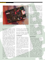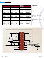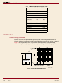
1
ISSUE 40, SUMMER 2001
SPECIAL EDITION – VIRTEX-II PLATFORM FPGA
Xcell journal
Issue 40
Summer 2001
THE AUTHORITATIVE JOURNAL FOR PROGRAMMABLE LOGIC USERS
PLATFORM FPGA
SPECIAL EDITION
XCELL JOURNAL
PRODUCTS
Virtex-II Devices Feature
Compatible Pinouts
TECHNOLOGY
Xilinx Digitally Controlled
Impedance Obsoletes
External Termination
Resistors
SOFTWARE
Integrated Synthesis
Environment Simplifies
Advanced System Design
NEWS
Advance Data Sheet
for 1.5V Virtex-II FPGAs
Cover Story
Mentor Graphics’ CEO Walden C. Rhines
Predicts New Era of Platform FPGA Design
Xilinx CEO Wim Roelandts
Talks About the Future of
Platform FPGAs
R
L E T T E R
F R O M
T H E
E D I T O R
Xilinx Virtex-II Platform FPGAs:
The Fusion of Silicon, Software, and Support
T
his is the first Special Edition of the Xcell Journal entirely devoted to one product line: the
state-of the-art Virtex®-II Platform FPGAs. This Virtex-II family is the result of the largest
silicon and software R&D effort in the history of programmable logic. Walden C. Rhines, CEO
of Mentor Graphics, notes in his Cover Story, the Virtex-II Platform FPGA gives a whole new level
of meaning to the concept of system-on-a-chip: “The Xilinx platform-based FPGA technology
brings programmability to the system-on-chip methodology.”
EDITOR IN CHIEF
Carlis Collins
[email protected]
408-879-4519
MANAGING EDITOR
Tom Durkin
[email protected]
530-272-5085
CREATIVE DIRECTOR
Andy Larg
DESIGN & ILLUSTRATION
Scott Blair
Dan Teie
BOARD OF ADVISORS
Dave Stieg
Mike Seither
Peter Alfke
Xcell journal
Xilinx, Inc.
2100 Logic Drive
San Jose, CA 95124-3450
Phone: 408-559-7778
FAX: 408-879-4780
©2001 Xilinx Inc.
All rights reserved.
Xcell is published quarterly. XILINX, the Xilinx logo,
CoolRunner, Spartan, and Virtex are registered trademarks of Xilinx Inc. Alliance Series, Xilinx Foundation
Series, AllianceCore, Foundation, IRL, LogiCORE,
SelectI/O, WebPACK, WebPOWERED, WebFITTER,
QPro, XPERTS, XtremeDSP, CORE Generator, Rocket
I/O, Fast Zero Power, SelectRAM, IP-Immersion,
System ACE, ChipScope, and all XC-prefix products are
trademarks, and The Programmable Logic Company is
a service mark of Xilinx Inc. Other brand or product
names are trademarks or registered trademarks of
their respective owners.
The articles, information, and other materials included in this issue are provided solely for the convenience of our readers. Xilinx makes no warranties,
express, implied, statutory, or otherwise, and accepts
no liability with respect to any such articles, information, or other materials or their use, and any use
thereof is solely at the risk of the user. Any person or
entity using such information in any way releases and
waives any claim it might have against Xilinx for any
loss, damage, or expense caused thereby.
Not only do the Virtex-II Platform FPGAs offer on-chip programmability, they also offer on-chip
processors in both hard and soft cores. In his View from the Top column, Xilinx CEO Wim
Roelandts explains how you can soon get an IBM PowerPC™ processor embedded within the programmable logic fabric, or you can choose the Xilinx MicroBlaze™ soft core processor – or you can
have both on the same Platform FPGA.
Read Peggy Abusaidi’s article “Virtex-II Platform FPGA Solution Launches New Era of High
Performance System Design” for an overview of the breakthrough technologies – including
SystemIO™, XCITE, IP-Immersion™, Digital Clock Managers, XtremeDSP™, and new design
software. There are numerous other articles in this Virtex-II Special Edition that describe these
technologies in depth, as well as examples of practical applications. For those who are looking for
“just the facts,” check out the Virtex-II Advance Brief Data Sheet and Virtex-II Product Guide.
Not only is this the first edition of Xcell Journal dedicated to one product line, it is also the first
issue in which I (Tom Durkin) have published as Managing Editor. I join Carlis Collins, Editor in
Chief, in continuing to bring you the best and most useful information in the programmable logic
industry. We are dedicated to keeping you informed of not only what field programmable logic
devices can do, but also what people are doing with our products. In coming issues, we will report
on the hunt for the last subatomic particle, the Higgs boson, at the Fermi National Accelerator
Laboratory, and we will investigate “evolutionary algorithms” that make Xilinx FPGAs capable of
redesigning themselves.
Even in these times of economic uncertainty, Wim Roelandts says it best: “Xilinx just keeps getting
better, and the future looks very bright.”
We hope you enjoy this Virtex-II Special Edition of the Xcell Journal – and we invite your comments
and suggestions.
Tom Durkin
Managing Editor
Overview
Page 4
Virtex-II Platform FPGA Solution
High-performance system design promises major improvements
in engineering productivity, silicon efficiency, and system flexibility.
Contents
Summer 2001
Virtex-II Platform FPGA Solution Launches
New Era of High Performance System Design...........................4
VIPswitch Partners with
Xilinx to Move Beyond ASICS ................................................7
Discontinuity at the Gate – A New Era in FPGA Design ..............8
Page 8
Extinct: Dinosaurs, Slide Rules, 8-Track Tapes,
and now... External Termination Resistors ..............................12
Discontinuity at the Gate
SystemIO Technology Promises High-Speed
Connectivity Across Multiple I/O Standards............................14
Cover Story
The Xilinx vision in programmable logic
will change how you do digital design.
Footprints in Silicon: Compatible Pinouts
in Virtex-II Devices Enhance Design Flexibility.........................16
The Future of Platform FPGAs ..............................................20
Technology
Page 12
XCITE – Xilinx Controlled
Impedance Technology
World’s first on-chip digitally controlled impedance
matching eliminates external termination resistors.
Networking
Page 14
SystemIO Technology Delivers
High-Speed Connectivity
Virtex-II Platform FPGAs accommodate multiple
I/O physical interfaces and networking protocols.
The Virtex-II DCM – Digital Clock Manager ............................24
Use Triple DES for Ultimate Virtex-II Design Protection .............29
Xilinx XtremeDSP Initiative Meets the Demand
for Extreme Performance and Flexibility.................................30
HyperTransport High Speed I/O ...........................................34
Virtex-II IP-Immersion™ Technology
Enables Next-Generation Platform FPGAs ...............................36
Using Xilinx ISE Software for High-Density Design...................38
Verification for Platform FPGA Design ....................................43
Designing High-Performance Memories and Multipliers.............45
Take Advantage of Leftover Multipliers and Block RAMs ...........48
Virtex-II Platform FPGAs Support System Packet
Interface Standards for Optical Networks ...............................50
System ACE Technology:
Configuration Manager Breakthrough ....................................52
View from the Top
Page 20
Insight Electronics Offers Two Virtex-II Development Boards......56
The Future of Platform FPGAs
Video Demonstration Board .................................................58
A look at the Xilinx philosophy behind
the Virtex family development.
Accelerate Time to Market with System-Level
Development Kits for Virtex-II Applications..............................60
Elantec DC-DC Converter Solution for Virtex FPGAs ..................63
4G Wireless Systems in Virtex-II...........................................66
New Products
Page 30
XtremeDSP Meets Demand
for Performance and Flexibility
Xilinx DSP solution boosts performance while conserving board
space for demanding wireless, networking, and video applications.
Debugging LVDS Signals in Virtex-II FPGAs.............................68
SiberBridge: A Virtex-II Platform FPGA
Interface for SiberCAM Arrays...............................................70
Year 2001Worldwide Xilinx Event Schedules..........................73
Virtex-II Data Sheet ............................................................74
Virtex-II Product Guide.........................................................84
Xilinx Product Reference Guide .............................................90
Virtex-II Data
Page 74
Virtex-II Data Sheet
Summary of Virtex-II Features
Advance Brief Data Sheet reveals specifications
for Virtex-II 1.5V Field Programmable Gate Arrays.
Xcell journal
For a Free Subscription to the Xcell Journal
enter your request at:
www.xilinx.com/forms/literature.htm
Overview
Platform FPGA
Virtex-II Platform FPGA Solution
Launches New Era of High
Performance System Design
The result of the largest silicon and software R&D effort in the history of programmable logic,
the Virtex-II Platform FPGA solution has produced major improvements in engineering productivity,
silicon efficiency, and system flexibility.
by Peggy Abusaidi
Product Marketing Manager, Xilinx, Inc.
[email protected]
The Xilinx Platform FPGA Initiative has
brought a new level of meaning to the concept of the integrated circuit. Components
that used to clutter up a printed circuit
board have migrated directly onto Virtex-II
devices themselves – providing superior
system integration previously unavailable
for programmable devices.
As the first embodiment of the Xilinx
Platform FGPA Initiative, the Virtex®-II
Platform FPGA solution ensures success in
today’s market of complex systems by
enabling rapid time-to-market and providing many of the features necessary to support today’s complex systems in a single
device. Consider:
• XCITE (Xilinx Controlled Impedance
TEchnology) breakthroughs have brought
DCI (Digitally Controlled Impedance)
onboard the FPGA platform. External
resistors are no longer needed to preserve
signal integrity on single-ended I/Os.
4
Xcell Journal
Summer 2001
Overview
In addition, the inherent flexibility of
Xilinx FPGA devices allows unlimited
design changes throughout the development and production
phases of system
design. This reduces
XCITE
SystemIO
design cycles from
Signal Integrity
Interface
years to months. As
shown in Figure 1,
IP-Immersion Fabric
the Platform FPGA is
• Active Interconnect
• Memory Rich Architecture
a combined suite of
• Embedded Multipliers
advanced design tools
and intellectual propDesign
Digital Clock
erties (IPs) that proEncryption
Manager
vide the ultimate system design platform
Figure 1 - Virtex-II Platform
for today’s cuttingFPGA Solution
edge applications.
• Up to 12 sophisticated, on-chip DCMs
(Digital Clock Managers) provide phase
shifting, clock de-skewing, and frequency
synthesis functions.
• Virtex-II Platform
FPGAs provides up
to 16 pre-engineered, glitch-free,
global clock multiplexers.
• Flexible SelectI/O™
Ultra
technology
supports 840 Mb/s
I/Os with as many as
1,108 user I/O
pins (554 differential I/O pairs).
• State-of-the-art SystemIO™ capability
supports interfaces for RapidIO™, PCIX, OIF SPI-4 (POS-PHY L3/L4,
Flexbus 4), and HyperTransport (formerly known as LDT – Lightning Data
Transport) standards.
IP-Immersion Architecture
Virtex-II IP-Immersion™ architecture is
specially designed to aid the seamless
integration of a wide variety of new hard-
Platform FPGA
macro building blocks, including
enhanced configurable logic blocks
(CLBs), memories, and multipliers. The
IP-Immersion architecture also enables
easy future integration of hard-macro
blocks that are now in development,
such as the IBM PowerPC™ processor
and high-speed serial I/Os. These new
hard macros dramatically increase the
data processing and transmission capabilities available in a single-chip solution.
Figure 2 shows a typical Virtex-II silicon
block diagram.
XCITE DCI
Xilinx is the first in the semiconductor
industry to provide on-chip digitally controlled impedance (DCI). As shown in
Figure 3, the DCI capability of the Virtex-II
FPGA enables designers to improve signal
integrity, while dramatically reducing the
number of external resistors needed for
impedance-matching components on print-
• Proprietary IP designs are protected
from piracy and reverse engineering by
on-chip Triple DES (Data Encrypted
Standard) bitstream encryption.
• High logic capacity Virtex-II devices
provide up to 10 million system gates.
• Platform FPGAs support up to 4.5 Mb
of memory.
• QDR/DDR (Quad Data Rate/
Double Data Rate) registers deliver
more than 400 Mb/s performance.
• Active Interconnect™ routing technology optimizes
throughput over fast, wide
buses.
• A single Virtex-II device
provides as many as
192 multipliers capable of up to 250
MHz of pipelined
performance.
• Virtex-II Platform FPGAs carry out more
than 600 billion multiply-and-accumulate
operations per second for XtremeDSP™
performance.
Summer 2001
Figure 2 - A typical Virtex-II silicon block diagram
Xcell Journal
5
Overview
Platform FPGA
ed circuit boards. Thus, Virtex-II FPGAs
with DCI technology reduce overall system costs and board layout complexity.
Furthermore, XCITE increases overall system reliability and assists designers in
meeting their time-to-market goals.
Active Interconnect Technology
With up to 10 million system gates, the
highest capacity in the industry, the
Virtex-II architecture with
Active Interconnect technology enables designers to
achieve optimized, predictable routing delays in
their designs, thus maximizing front-end design
performance.
On-chip
support for high-speed I/O
standards with up to 1,108
user I/O pins is included.
Advanced DSP applications, such as echo cancellation, forward error-correction, and image compression/decompression,
all benefit from the abundance of embedded highspeed 18-bit x 18-bit multipliers within the Virtex-II Platform
FPGAs. The Virtex-II solution enables
rapid development of the two most technically challenging system applications:
data communications and digital signal
processing. These system applications are
characterized by the need for high logic
integration, fast and complex routing of
wide buses, extensive pipeline, and
requirements for FIFO memory.
Software Design Tools
The Virtex-II solution is empowered by a
suite of sophisticated design tools that support the industry’s fastest run times and
most advanced design methodologies. This
combination delivers unequalled productivity and the fastest possible time-to-market of any logic solution available today.
The Xilinx innovative, incremental design
flow facilitates efficient “what if ” analyses,
accelerates timing closure, and increases
system performance. High-level floorplanning and modular design make it easy to
6
Xcell Journal
realize the promise of true team design.
The Xilinx System Generator, together
with The MathWorks’ MATLAB™ and
Simulink™ modeling programs, provides
a powerful design package using tools
already familiar to system and DSP designers. These software tools and the library of
Xilinx Smart-IP™ cores, which are preoptimized for Xilinx devices, enable
accelerated timing simulation, and even
powerful static timing analysis – Xilinx
design tools ensure that designers and
engineers make the most of their time.
Board-level verification is supported
through STAMP (Static Timing Analysis
Modeling Procedure) and LMG (Logic
Modeling Group) smart models. The
Xilinx ChipScope ILA (Integrated Logic
Analyzer) is a revolutionary
tool for real-time, on-chip
debugging. Logic analysis
cores can be inserted into
the actual design, and the
real-time behavior of any
signal can be displayed,
analyzed, and even exported
High-Speed
for board-level analysis,
Logic
using industry leading logic
analyzers. Results are
extremely
accurate.
ChipScope ILA easily handles wide buses, complex
With XCITE
triggering, and multiple
clocks, which cuts debugWithout XCITE
ging time from weeks to
just a few hours. ChipScope
Figure 3 - Virtex-II XCITE capability
ILA is integrated with
industry leaders’ tools,
designers to increase overall design proincluding Agilent Technologies’ 16700
ductivity and reduce time to market.
Series logic analyzers and Synplicity’s
Engineering productivity is also enhanced
Certify tools.
by the Xilinx IP delivery process.
From Platform to Launchpad
Everything from IP building blocks to
A new era in system platform design has
sophisticated IP cores for design reuse is at
begun. The Virtex-II Platform FPGA fully
the designer’s command with Xilinx
integrates soft- and hard-IP cores by partCORE Generator™ software. Up-to-thenering with the world’s leading technology
minute new IP cores and IP updates are
companies. By introducing the poweravailable from the Xilinx IP Center at
house Virtex-II solution, Xilinx has set the
www.xilinx.com/ipcenter/.
industry’s highest possible benchmark in
performance and flexibility. Together, the
Verification Solution
unique features of the revolutionary
One of today’s biggest challenges is the
Virtex-II Platform FPGA solution provide
verification bottleneck. Platform FPGA
the ultimate launchpad for system connecprogrammability makes many time-contivity, DSP, and processing applications.
suming verification tasks, such as chipWith the rich system feature set, designers
level signal integrity analysis and scan
can develop new architectures with Virtexinsertion, unnecessary. Xilinx design tools
II Platform FPGAs at the heart of their
allow efficient use of desktop and in-lab
designs for tomorrow’s optical networking,
verification times. With complete support
SANs (Storage Area Networks), VoIP
for all verification checkpoints – including
(Voice-over-Internet-Protocol), video, and
RTL (Register Transfer Level) simulation,
wireless applications.
Summer 2001
Success Story
XCITE
VIPswitch Partners with
Xilinx to Move Beyond ASICs
Remotely programmable chips are a perfect fit
for new line of Optical Terabit Routers.
by Beverly Wilks
Director, Marketing Communications, VIPswitch
[email protected]
offered the best price, reliability, and the
smallest footprint. It really provided just
what we needed.”
When engineers at VIPswitch set out to
design their newest product, the Open
Metro Networks V-MAN 160G optical
Terabit switch/router, they were looking for
a flexible and cost-effective solution that
would enable them to bring their innovative technology to the market, ahead of the
competition. The VIPswitch design team
also needed the ability to reprogram the
system in the field, to provide their customers with upgrades even after installation at the customer facility. VIPswitch
found the reprogrammable Xilinx Virtex-II
FPGAs met each of these requirements.
VIPswitch also based their selection on
the Xilinx Controlled Impedance
Technology (XCITE™) feature, which is
unique to Virtex-II FPGAs. This capability uses two external reference resistors to
hold input and output impedance for
hundreds of I/O pins. Benefits include a
reduction in on-board resistors that significantly reduce system costs and board respins. Eliminating hundreds of resistors
using the XCITE technology, VIPswitch
designers reduced board real estate and
complexity, and increased reliability.
“In adopting FPGAs in our designs,
rather than ASICs, we are safeguarding
ourselves and our customers against costly future upgrades due to the ever changing requirements in this space,” said
Brian Bowyer, senior vice president of
product development and program management at VIPswitch. “With Xilinx
FPGAs, our switch/router will be the first
that can be fully implemented and reprogrammed without relying on an ASIC.
The technologically advanced Virtex-II
product family enabled us to overcome
cost, dissipation, performance, and footprint issues that are usually found in traditional FPGAs. It was hard to justify the
cost of an ASIC when Virtex-II FPGAs
Summer 2001
“The XCITE capability enabled our
design team to use the board more efficiently, resulting in fewer board re-spins
and lower PCB costs,” said Yvon
Gaudreau, senior manager of hardware
development for VIPswitch. “Virtex-II
FPGAs provided us with the ideal platform for our design.”
“VIPswitch’s application of Xilinx
FPGAs further demonstrates our penetration into the ASIC market,” said Clay
Johnson, vice president of the Advanced
Product Group for Xilinx. “With everincreasing bandwidth requirements, system engineers face extreme signal integrity issues. Our XCITE signal integrity
technology in the Virtex-II FPGAs dra-
matically simplifies board design and
maximizes system performance.”
Conclusion
VIPswitch experienced the many benefits of
using Virtex-II devices. Virtex-II FPGAs
are the first offering in the new Xilinx
Platform FPGA family and represent a
flexible solution that integrates a wide
variety of hard and soft IP cores on a single device whose hardware and firmware
can be upgraded at any time. The programmability of the architecture reduces
system development time yet enables a
single Platform FPGA to be targeted at
multiple applications.
About VIPswitch
VIPswitch is a privately
held company with offices
in Boston and Montreal.
For more information,
please visit VIPswitch
on the web at:
www.VIPswitch.com,
send an email to
[email protected],
or call 800-638-2677.
Xcell Journal
7
Cover Story
Mentor Graphics CEO
Discontinuity at
the Gate – A New
Era in FPGA Design
The Xilinx vision in programmable logic will change how you
do digital design. Mentor Graphics has recognized this and is
committed to the FPGA market.
by Walden C. Rhines
Chairman and CEO, Mentor Graphics Corporation
[email protected]
What happens when you give the design
community a field-programmable hardware
platform that contains 10 million system
gates, 300+ MHz internal clock speeds,
gigabit serial I/O performance, and IP
immersion technology? You create an
opportunity for an entirely new complex
design methodology. By providing such
robust capabilities in a programmable format, you create a discontinuity in the industry that removes previous cost and technology barriers from the product development
process. The Xilinx Virtex-II Platform
FPGA family embodies this emerging technology, and has provided the catalyst to
change our current design methodologies.
Today it is estimated that there are 20,000
custom or semi-custom chip designers, and
this number is growing very slowly, as
shown in Figure 1. Under the current structure, issues including design styles, verification methodologies, NRE charges, risk, and
software development inhibit how many circuits can be attempted each year. Creating a
standard platform for development removes
these limitations, and allows the number of
potential designers to grow by an order of
magnitude, to 200,000. This massive influx
of potential designers creates a new brain
pool for innovation.
8
Xcell Journal
Summer 2001
Cover Story
FPGAs Coming of Age
In contrast, FPGA technology has taken only five years
to get to the same level of
functionality as ASICs.
FPGA
technology
has
uniquely solved the same
problems the ASIC methodology addressed, but along
the way it also minimized
the NRE, risk, and manufacturing issues involved as
illustrated in Figure 3.
Today, the Xilinx Virtex-II
technology is a legitimate
ASIC replacement. When
combined with leading-edge
EDA software, Virtex-II
FPGAs provide the electronics industry with a new,
exciting path for growth and
innovation. FPGAs are now
the key vehicle driving the
state-of-the-art for new electronic systems.
The Xilinx platform-based
FPGA technology brings proSummer 2001
100,000,000
Gates Per Chip
10,000,000
1,000,000
~200,000
100,000
~20,000
10,000
1,000
~2000
100
10
1
19
80
19
82
19
84
19
86
19
88
19
90
19
92
19
94
19
80
19
96
19
99
20
01
20
03
20
05
20
07
20
09
The path to harmony
between design tools and
actual silicon is extremely
challenging. For example, as
shown in Figure 2, in the
ASIC world it took 15 years
to merge the silicon process
with a solid design methodology based on reliable and
functional EDA software.
ASIC technology became the
driving force in the industry.
The process that began surrounding this technology
created an effective solution
for the electronics industry,
which led to growth and
innovation. But the ASIC
process has matured to the
point where it is applicable
more for extremely high-end
design, and it is slowly moving out of reach for the mass
market.
Custom IC Designers (Slide 5)
Figure 1 - Gate-to-designer ratio
Mentor Graphics CEO
grammability to the Systemon-Chip (SoC) methodology.
Using a 0.15µ, 8-layer metal
process with 0.12µ high-speed
transistors, Virtex-II FPGAs
provide designers with the
performance and density they
need to create an SOC design.
With features like digital
clock management, select I/O
ultra technology, and active
interconnect, designers can
spend more time on functional verification, knowing that
the main silicon issues and
problems have already been
solved. In addition, with IP
immersion technology, FPGA
designers can now work at a
much higher level of abstraction and move the “gates
per day” metric to a level
where silicon utilization is
maximized.
Platform-Based FPGAs –
The Value of History
Figure 2. Evolution of ASIC and FPGA design methodologies
Cumulative
NRE+Unit Cost
PLD .25µ
ASIC .15µ
ASIC Costs
Start higher,
but slope is
flatter.
PLD .15µ
ASIC .25µ
Cumulative
Volume K Units
For each technology advance,
PLDs become more cost effective.
Figure 3. FPGA to ASIC crossover improves with process
Creating standards and putting boundary conditions on
a design process can accelerate
circuit development and
shorten time to market. The
ASIC SOC development
process in place today is an
open-ended approach to
design with almost an infinite
degree of freedom. This freedom provides flexibility and
has enabled the creation of
extremely complicated circuits, but it has also created a
high risk methodology with a
steep learning curve.
In contrast, platform-based
FPGAs provide a structured
approach to design. From the
designer’s point of view, the
beauty of creating an FPGA is
that the FPGA vendors worry
about all the issues of the
design process (silicon,
methodology, and software).
Xcell Journal
9
Cover Story
Mentor Graphics CEO
ASIC SoCs by addressing IP
integration issues, as shown
in Figure 4. The Xilinx IP
immersion technology maximizes performance and
density by providing a fixed
and proven structure to
integrate hard and soft IP
into the silicon architecture.
Figure 4 - Platform-based FPGAs integrate IP to user-defined logic
From the FPGA vendor’s point of view,
they need to provide their customers with
a solution that enables high-quality,
repeatable results.
Platform-based FPGAs have taken the
problems found by previous ASIC SoC
designers and minimized them by pro-
IP Immersion
Designing an ASIC SoC requires a highly
experienced team of engineers from multiple disciplines. This team must learn
how to use a processor, develop software
on it, and connect IP into the system.
These learning curves are long and riddled
Today, the Xilinx Virtex-II technology is a legitimate ASIC replacement.
When combined with leading-edge EDA software, Virtex-II FPGAs provide the
electronics industry with a new, exciting path for growth and innovation.
— Walden C. Rhines, Chairman and CEO, Mentor Graphics
viding a proven, recommended path for
success. In the history of electronic
design, innovation and productivity are
at their peak when proven methodologies
permeate the industry.
10
Xcell Journal
with mistakes. And, because all design
blocks come from different places, integration rarely works on the first try.
Platform-based FPGAs solve some of the
big issues that limit the development of
Platform-based
FPGAs
using embedded processors
will be the next key technology that will push
FPGA design forward. By
limiting support to only
certain CPU architectures,
all integration information
is predefined for functions
such as control signals,
clocks, and data buses. Soft
IP is pre-engineered to
work with these predefined buses, so the
designer just needs to connect these fixed IP objects
to the buses. For the userdefined section of the chip, the design
has been made easier because its boundary conditions are known.
To take advantage of these fixed-CPU
platform-based FPGAs, designers will
look for new applications and uses. Since
the cost of implementation will be in
everyone’s reach, we should see a resurgence of the garage-shop mentality and
new out-of-the-box thinking.
Enabling Innovation Together
At Mentor Graphics, we enjoy collaborating with a partner that looks at the big
picture and asks, “How do I change the
future?” The Xilinx vision in programmable logic will change how we do digital
design. Mentor has recognized this and is
committed to the FPGA market. We continue to develop point tools and solutions
to solve the tough design problems.
Mentor realizes that dedicated FPGA
flows, tested and integrated tightly with
the vendor software, will provide the technology that will “Enable Innovation” for
the future of the electronic industry.
Summer 2001
The only IP Center
worth diving into.
Xilinx IP Center is the only web portal that brings together cores, reference
designs, design reuse tools, and design services. Everything the system designer could wish for.
SmartSearch™ engine
Get to the cores and design tools you want fast, and access our AllianceCORE™ and XPERT™
Partners with the industry’s best search engine. SmartSearch means easy
access, and easy downloads.
Complete solutions
Supporting our powerhouse programmable logic products like Virtex™ and
Spartan® FPGAs, Xilinx IP Center offers you the total solution you need.
Try before you buy
At Xilinx IP Center, you can try the most efficient IP solutions available today before you buy.
It’s just one more reason why Xilinx is the industry leader in IP. Visit www.xilinx.com/ipcenter and
dive into it today.
The Programmable Logic CompanySM
www.xilinx.com
© 2001 Xilinx, Inc., All rights reserved. The Xilinx name, Xilinx logo and Spartan logo are registered trademarks, AllianceCORE, IP Center, SmartSearch,
Virtex and XPERTs are trademarks and The Programmable Logic Company is a service mark of Xilinx, Inc.
Technology
XCITE
Extinct:
Dinosaurs, Slide Rules,
8-Track Tapes,
and now... External
Termination Resistors
Xilinx Virtex-II Platform FPGAs
now feature the world’s first
on-chip digitally controlled
impedance-matching technology.
by Mark Alexander
Product Applications Engineer, Xilinx Inc.
[email protected]
Termination resistors as we know them are
about to vanish. XCITE (Xilinx Controlled
Impedance TEchnology) – the adaptive
on-chip termination system now available
in the Virtex®-II family of FPGAs – banishes external resistors, making PCBs
(Printed Circuit Boards) less expensive, easier to design, and more reliable.
High performance systems require signal
frequencies in the hundreds of megahertz,
necessitating
impedance
matching
between device I/Os and PCB traces. In
the past, as clock speeds increased and I/O
standards changed, system engineers and
PCB designers learned signal termination
techniques, using external resistors to
match impedances. Over time, more and
more resistors were required to account
for the increasing widths of large data
busses. With the advent of 1,500-pin
packages, discrete resistor placement
became a major challenge.
External termination resistors necessitate
more board traces and increased PCB part
counts, making the layout process more
time consuming. These factors lead to
higher manufacturing costs and longer
times to market. Additionally, sky-high
part counts do not help system reliability
either – each additional part increases the
risk of a system failure.
Here at Xilinx, our Virtex-II team wanted
designers to have a worry-free solution to
terminating high-speed signals, so we
invented XCITE I/O. All Virtex-II I/O pins
are equipped with XCITE, making impedance matching a pre-engineered solution.
12
Xcell Journal
Summer 2001
Technology
Not only does XCITE make PCBs less complicated, it actually improves signal quality.
With termination residing inside the device
instead of a few centimeters away, stub reflection is eliminated as a design factor.
XCITE can be used to terminate a variety
of I/O standards. All variants of HSTL
(High-Speed Transistor Logic), SSTL
(Solid State Track Link), GTL (Gunning
Transceiver Logic), and LVCMOS (Low
Voltage Complementary Metal Oxide
Semiconductor) are supported. Designers
XCITE is a better solution than discrete
resistors because it continually adjusts
the termination impedance to match the
VTT = VCCO/2
VTT = VCCO/2
PCB trace impedance. In
HSTL II Transmitter
HSTL II Receiver
conventional systems,
temperature and voltage
50 Ω
variations can play havoc
with the carefully engineered impedances of a
HSTL Class II without XCITE
signal
path.
With
HSTL II DCI Receiver
XCITE, the termination
HSTL II DCI Transmitter
V
V
impedance of the driver
or receiver is continually
50 Ω
compared against a reference resistor. Over the
full range of temperature,
voltage, and process variHSTL Class II with XCITE
ations, XCITE maintains
Figure 1 - Termination resistors on-chip
a tight impedance match.
CCO
CCO
I/O counts will continue to increase, and
so will clock speeds. The Virtex-II architecture makes this situation livable by offering
the latest high-speed I/O standards without
the difficulties of external termination
resistors (or punchcards).
need only specify their signal I/O standard
in the software. In the case of the bidirectional standard HSTL Class II, the external resistors usually required for the
source and destination are implemented
on-chip (see Figure 1). The PCB designer
only has to route a 50Ω trace from the
output of one Virtex-II device to the
input of another (see Figure 2).
For more information on XCITE,
consult Chapter 2 of the Virtex-II
Platform FPGA Handbook, which can
be found online at www.xilinx.com/
products/virtex/handbook/.
Resistors
XCITE
How XCITE Works
Both series and parallel termination schemes can
be implemented with XCITE. While parallel termination is realized on-chip with pull-up and pulldown resistors, series termination is realized with
a controlled impedance driver. The output impedance of this driver is set to equal the impedance
of the PCB trace. XCITE transmitters can operate
with parallel termination, a controlled-impedance
driver, or a combination of the two; XCITE
receivers can operate with parallel termination.
Because of the way it is implemented, parallel
XCITE termination may terminate to either the
full VCCO voltage or to a VCCO/2 (as in the HSTL
Class II standard).
XCITE matches its impedance to a pair of external reference resistors. These reference resistors
are connected to dual-function pins on the
Virtex-II device. Each of the eight I/O banks has
two of these dual-function pins, VRN and VRP. If
XCITE is not used in a bank, these pins are available for user I/O.
Reference resistors are chosen to have the same
impedance value as the PCB trace. XCITE can match
any impedance from 25Ω to 100Ω. The XCITE I/O
matches the reference value by selectively enabling
or disabling parallel transistors. A coarse impedance
adjustment is made during the device startup
sequence, accounting for process variation. During
device operation, fine adjustments are continually
made to ensure that I/O impedance stays matched
as temperature and voltage drift.
XCITE is implemented in software either by direct
HDL instantiation or through the IOSTANDARD
attribute in the constraints file. The following are
examples of each:
VHDL
VTT
Later
PCB implementing HSTL Class II without XCITE
HSTL_DCI_buffer: OBUF_HSTL_I_DCI
port map (I => data_out, O => data_out_DCI);
UCF or NCF
NET <net name> IOSTANDARD =
OBUF_LVDCI_25;
PCB implementing HSTL Class II with XCITE
(Where <net name> is the name of the net between
the IPAD and IBUF, or OPAD and OBUF. For HDL designs,
this name is the same as the port name.)
Figure 2
Summer 2001
Xcell Journal
13
Innovations
Networking
SystemIO Technology Promises
High-Speed Connectivity Across
Multiple I/O Standards
As implemented via Virtex-II Platform FPGAs, SystemIO technology addresses both
the physical interfaces and networking protocols for high bandwidth connectivity and throughput.
by Rina Raman
APG Director of Applications Engineering, Xilinx
[email protected]
Moore’s Law, which predicts computer
processor speeds will double approximately
every 18 months, has proved to be remarkably accurate for more than 35 years. The
exponential increases in processor speeds
have enabled ever higher bandwidth networking. The problem now, however, is
that I/O busses have only doubled their frequencies every three years. Thus, the level of
performance of a system at the board level is
now dictated not by the speed of processor
but by the limits of the I/O bus. While
delivering greater bandwidth, numerous
emerging I/O standards – RapidIO™,
POS-PHY™ Level 4, 10 Gb/s Ethernet,
XAUI, HyperTransport™, Fibre Channel,
among others – provide various choices and
architectural options. Xilinx Virtex®-II
Platform FPGAs address this proliferation
of standards with the SystemIO™ solution,
which provides system interconnectivity at
both the physical I/O interface and the networking protocol levels.
I/O Signaling Standards
Virtex-II devices are designed to support
many signaling standards, including essential interfaces to high performance systems.
For instance, memory devices operating
above 180 MHz can only use SSTL (Stub
Series Terminated Logic) or HSTL (High
Speed Transceiver Logic) I/O standards.
14
Xcell Journal
Many I/O standards – including the traditional switching standards of LVCMOS
(Low Voltage CMOS), memory interfaces
of HSTL and SSTL, and even LVDS (Low
Voltage Differential Signaling) – are not
keeping pace with the increased demand
for more bandwidth. Designers have tried
to overcome these bandwidth limits by
using more pins and/or larger bus widths.
This has made the traditional I/O standards more “pin-intensive.” Significant
problems arise as pin counts grow into the
hundreds and thousands, creating routing
congestion on printed circuit boards.
Although Virtex-II Platform FPGAs can
easily route inside the device, it is extremely difficult to interface with all the pins on
a PCB. More layers of interconnect routing in the PCB cause dramatic increases in
overall board costs. The number of pins
running these standards also produces
problematic electromagnetic interference.
Beyond the Shared PCI Bus
Additionally, the most popular bus architecture is a “shared” medium where multiple entities use the same bus, each waiting in turn for its opportunity to complete its transaction. As the size of audio
and video data streams increase, the waiting period gets longer. Ultimately, overall
performance decreases along with performance predictability. Therefore, the
industry trend is to move from a shared
bus to a point-to-point link, typically
configured as a switched fabric.
Decreased bus efficiency has many causes.
Although we may have economies of scale
for most applications, the shared PCI bus
compromises graphics performance. For
example, when using a PCI graphics card,
the graphics card needs to refresh every few
milliseconds. In order to do this, it needs to
have immediate and frequent access to the
PCI bus. As a result, other PCI cards cannot
send huge data bursts. This is because the
PCI arbiter is designed to ensure that no one
component can send large bursts of data.
The most popular shared bus is the PCI
(Peripheral Component Interconnect) bus.
It has become a general-purpose bus for
personal computers and embedded systems supporting many different applications. A 33 MHz, 32-bit PCI bus can support one source and five destinations with
an overall bandwidth of 1 Gb/s. At 66
MHz and 64 bits, the bandwidth rises to 4
Gb/s, but then the bus only supports one
source and two destinations. The PCI
shared bus structure has diminishing performance returns, is less predictable than a
point-to-point solution, and is limited to
internal systems.
Ideally, we would like to establish a link
and then “burst” the data over a really
wide data bus. This would maximize bus
efficiency. Bus efficiency is highest with
long bursts.
Summer 2001
Innovations
In graphics intensive applications, an AGP
(Advanced Graphics Port) is a much better
choice than a PCI bus. Although AGP is
based on PCI technology, it is designed
especially for the high throughput requirements of 3D graphics. Rather than
using the shared
System-Synchronous
PCI bus for graphics
Parallel
data transmission,
the AGP introduces
• PCI-66
a dedicated point• PCI-6
CI-64/66
to-point channel so
• PCI-X133
33
that the graphics
controller
can
Source-Synchronous
directly access main
Parallel
memory. Virtex-II
Platform
FPGAs
• RapidIO
support both PCI
• LDT
• SPI-4
and AGP I/O stan• POS-PHY3
dards, as well as
• POS-PHY4
many others.
ture supports universal switching capabilities to these new standards, making them
the logical choice for system designers.
As we mentioned earlier, the key advantage of SystemIO technology is that it
Switched Fabric Advantages
A switched fabric is more scalable for high
performance and ultimately, offers a lower
cost solution for high bandwidth applications. In the past, data rates weren’t high
enough to warrant using a switched fabric
within a system, because this would require
many point-to-point connections and
would increase system complexity. With
the dramatic increases in performance
enabled by the new interface standards,
however, switched fabric solutions are
becoming cost-effective.
With the huge existing PCI infrastructure,
bridges are needed to interconnect the various high-performance I/O standards.
Virtex-II Platform FPGAs are key building
blocks in the transition from shared buses
to switched fabrics. The Virtex-II architecSummer 2001
4) – This standard is defined for 10
Gb/s Ethernet applications and optical
networking applications demanding
OC-192 performance.
• 10 Gb/s Ethernet – Using an XGMII
interface, this IEEE
standard is positioned
to drive the converAdvanced
Memory
gence of LAN and
Interfaces
WAN technologies.
• ZBT SSRAM
• DDR SDRAM
SDRA
• QDR
QD SSRAM
• CAM
Multi-Gigabit
Serial*
• Multi-Gigabi
Multi-Gigabit Backplanes
• InfiniBand
• Gigabit Ethernet
• 10 Gigabit Ethernet - XAUI
• Fibre Channel
• FlexBus3
Another drawback
• FlexBus4
of the PCI bus is
• XGMII
that it has no termination – or rather, it is series terminated.
This means that it relies on reflective wave
switching. Although reflective wave switching is inexpensive and has relatively low
power consumption, series termination
requires the system to wait for the reflection, so we lose valuable time.
*Available in next generation
provides both physical interfaces as well
as various cores that support the network
protocols. With the transition from
shared busses to switched fabrics comes a
variety of different source-synchronous
(parallel) protocols. The following are
some of the leading source-synchronous
standards that are emerging:
• RapidIO – Originally organized to support the processor and local bus markets,
the RapidIO interconnect architecture
has been embraced by the networking
and storage markets.
• InfiniBand™ – Founded by an industry
consortium, InfiniBand targets remote
storage, servers, and networking devices.
• HyperTransport – Formerly known as
LDT (Lightning Data Transport),
HyperTransport was jointly developed by
AMD and API to replace PCI in highspeed computing applications. It has
gained some acceptance in the networking space.
• OIF - SPI4 (Optical Internetworking
Forum - System Packet Interface Level
Networking
In addition, there are
emerging serial channel standards as well.
Two of the most popular standards in this
arena are:
• Fibre Channel – A
favorite for the storage area networking
(SAN) market, Fibre
Channel uses optical
fiber, coaxial cable,
and/or twisted-pair
telephone wire.
• XAUI (pronounced ZOW-ee) – This
new standard targets 10 Gb/s serial
channels by bonding four 3.125 Gb/s
transceivers. XAUI targets the OC-192
and 10 Gb/s Ethernet markets for WAN
and LAN routers.
Conclusion
Having a solution that supports all these various system interfaces is crucial to success in
the marketplace. The Virtex-II Platform
FPGAs’ SystemIO solution offers exactly
this – support for physical interfaces as well
as cores that support the network protocols
for all the common and emerging system
I/O interfaces. Virtex-II FPGAs enable high
performance interfaces to memories from
Cypress, IDT, Micron, SiberCore, GSI
Technology and others, as well as interfaces
to networking ASSPs (Application Specific
Standard Parts) from vendors such as
AMCC, PMC Sierra, and Vitesse. Now,
with Virtex-II SystemIO solution, you can
pick any standard, and any vendor offering
that standard in their ASSPs, and rest
assured that Xilinx Virtex-II Platform
FPGAs will support that standard.
Xcell Journal
15
Packaging
Pinouts
Footprints
inSilicon:
Compatible Pinouts in
Virtex-II Devices Enhance
Design Flexibility
Advanced Virtex-II architecture allows you to change
FPGA densities without changing PCB designs.
by Jean-Louis Brelet
Product Applications Manager, Xilinx
[email protected]
Mid-production design changes are common in
today's fast-paced production environment.
These changes often force you to create new PC
boards, and incur long delays, because you
require a larger (or smaller) FPGA to meet your
new design requirements. Design changes are
inevitable, but now there is a way make them
much easier, faster, and far less expensive.
The Virtex™-II FPGA family offers unique
pinout/package migration paths that maintain
PCB footprint compatibility across different
device densities and packages. You can increase
or decrease density from 40K to 10M system
gates on the same PCB footprint. What’s more,
you can change some chip packages without
losing footprint compatibility. With a little
planning, you won't have to replace your PC
boards when you upgrade to a new FPGA.
The Virtex-II family consists of 12 devices
offered in 10 different packages. While, of
course, they are not completely interchangeable, strategic Xilinx engineering has delivered unparalleled design migration flexibility.
This article explains the rules and advantages
of compatible device/package pinouts and
footprints – and features a special transparency overlay that graphically illustrates compatible pinout migration.
Packaging
All 10 Virtex-II packages are ball grid
arrays (BGAs):
• CS denotes wire-bond chip-scale BGA
(0.80 mm pitch)
- CS144 in 0.8 mm pitch
• FG denotes wire-bond fine-pitch BGA
(1.00 mm pitch)
- FG256
- FG456
- FG676
• FF denotes flip-chip fine-pitch BGA
(1.00 mm pitch)
- FF896
- FF1152
- FF1517
16
Xcell Journal
Summer 2001
Pinouts
Bank 4
Bank 1
Bank 0
Bank 4
Bank 5
Bank 7
Bank 5
Bank 2
Bank 1
Bank 3
- BG728
Bank 0
Bank 7
- BG575
Bank 2
• BG denotes standard BGA
(1.27 mm pitch)
Bank 3
Packaging
For more details, see the Virtex-II Data Sheet
(www.xilinx.com/partinfo/ds031.htm), or
Chapter 4 of the Virtex-II Platform FPGA
User Guide (www.xilinx.com/products/virtex/handbook/).
Pin Types
Virtex-II devices have the following pins:
• Programmable user I/Os (from 88 in the
CS144 and FG256 packages to 1,108 in
the FF1517 package)
• Power and ground pins
• Control pins, including configuration,
JTAG, and special purpose pins such as
VBATT.
All the pin types are similar regardless of
the device/package combination. The
number of control pins is always 16,
including VBATT. The number of
power/ground pins and user I/O pins,
however, depends on each device/package
combination.
The total number of user I/Os available
for each device/package is based on two
limitations:
• Maximum number of pins on the package
(See Virtex-II Data Sheet – Module 1,
“Wire-Bond Packages Information” and
“Flip-Chip Packages Information.”)
Bank 6
- BF957
Bank 6
• BF denotes flip-chip BGA
(1.27 mm pitch)
Figure 1 - Virtex-II I/O banks for wire-bond
packages (CS, FG, and BG)
Figure 2 - Virtex-II I/O banks for flip-chip
packages (FF and BF)
to support I/O standards from 1.5V to
3.3V, are connected to pins that serve
banks of I/O pins.
grams provided in Chapter 4 of the
Virtex-II Platform FPGA User Guide are
top views of the package.
The bank organization depends on the
package type. Figure 1 represents a top
view for wire-bond packages (CS, FG, and
BG) with banks in clockwise order, and
Figure 2 shows a top view for flip-chip
packages (FF and BF) with banks in counterclockwise order. All the pinout dia-
For example, Table 1 illustrates the maximum number of pins per bank for the
FG256 package. The user I/O count
includes the VREF, VRP/VRN, and nondedicated configuration pins. The definition of each pin type is in the Virtex-II
Data Sheet – Module 4.
Device
XC2V40
XC2V80
XC2V250
XC2V500
XC2V1000
Total user I/Os
88
120
172
172
172
Bank 0 - user I/Os
12
12
20
20
20
Bank 0 - VCCO_0
3
3
3
3
3
Bank 1 - user I/Os
12
12
20
20
20
Bank 1 - VCCO_1
3
3
3
3
3
Bank 2 - user I/Os
10
18
22
22
22
Bank 2 - VCCO_2
3
3
3
3
3
Bank 3 - user I/Os
10
18
22
22
22
Bank 3 - VCCO_3
3
3
3
3
3
Bank 4 - user I/Os
12
12
22
22
22
Bank 4 - VCCO_4
3
3
3
3
3
• Maximum number of pads on the die
(different for wire-bond versus flip-chip
applications).
Bank 5 - user I/Os
12
12
22
22
22
Bank 5 - VCCO_5
3
3
3
3
3
Bank 6 - user I/Os
10
18
22
22
22
For example, the FF1517 package limits the
maximum number of user I/Os to 1,108
pins in the XC2V10000 device.
Bank 6 - VCCO_6
3
3
3
3
3
Bank 7 - user I/Os
10
18
22
22
22
Bank 7 - VCCO_7
3
3
3
3
3
I/O Banking
Dedicated pins
16
16
16
16
16
VCCAUX (3.3 V)
4
4
4
4
4
VCCINT (1.5V)
8
8
8
8
8
Ground
32
32
32
32
32
Virtex-II user I/Os are split into eight
banks to provide more flexibility in I/O
standards choices and XCITE capabilities.
The VCCO and VREF voltages, necessary
Summer 2001
Table 1 - Pinouts in the FG256 package
Xcell Journal
17
Pinouts
Packaging
Pinout Compatibility
Pinout compatibility across different
devices gives you a major advantage when
designing your application. All the devices
in a particular package are 100% pinout
compatible. The 16 control pins are always
located on the same package balls. All
power and ground balls are at the same
package ball location. Each programmable
user I/O has the same ball name in the
same bank, and the same package ball location, including LVDS (Low Voltage
Differential Signaling) pairs. The main
benefit here is that you can re-use the same
PCB footprint for as many as six devices of
different densities in one package.
For example, a BF957 package with its fixed
ball assignment accommodates the
XC2V2000, XC2V3000, XC2V4000,
XC2V6000, XC2V8000, and XC2V10000
devices. This represents a 5X density ratio in
a single footprint.
Table 2 summarizes the pinout compatibility
of the entire Virtex-II family.
The full pinout compatibility of each of the
10 packages can be found in the individual
package pinout tables in Module 4 of the
Virtex-II Data Sheet. No Connect (NC)
Package
information is provided for the smaller
devices in each package. When two devices
have a No Connect, the NC of the larger
device matches the NC of the smaller one to
facilitate pinout migration.
Pinout Compatibility Across Packages
Virtex-II devices offer even more flexibility,
because two package pairs are both pinout
and footprint compatible. In other words,
devices that are already pinout compatible
within a package type are also footprint compatible with another package type. The two
pinout/footprint compatible package pairs
are wire-bond FG456 & FG676 and flipchip FF896 & FF1152.
This additional flexibility allows you to produce a single PCB that can accommodate
anything from the XC2V1000 in FF896 to
the XC2V10000 in FF1152. This represents
footprint compatibility across eight devices,
for a density ratio of 10X.
As shown in Figure-3, the FF896 pinout
diagram is drawn on a transparent page to
demonstrate the footprint compatibility
with the FF1152. Complete definitions of
all the pin types listed in the pinout diagram are available in Module 4 of the
Virtex-II Data Sheet.
CS144 FG256 FG456 & FG676 FF896 & FF1152
FF1517 BG575 BG728
BF957
Min User I/Os
88
88
200
432
912
328
456
624
Max User I/Os
92
172
484
824
1,108
408
516
684
XC2V40
✓
✓
XC2V80
✓
✓
XC2V250
✓
✓
✓
XC2V500
✓
✓
XC2V1000
✓
✓
✓
✓
XC2V1500
✓
✓
✓
XC2V2000
✓
✓
✓
XC2V3000
✓
✓
- Pin location is referenced by
“Letter/Number” (for example, A2).
- “Letter” indicates a row.
- “Number” indicates a column.
- FF1152 Letter/Number = FF896
Letter + 2 / Number +2
For example, the A2 pin of FF896 is the
C4 pin of FF1152.
Using the above information, any user I/O
of one package can be easily located in the
second one. If digitally controlled impedance technology is used in Bank 4, you
have the choice between:
• If SelectMAP (parallel configuration) is
not used, the alternative ALT_VRP and
ALT_VRN pins can be used as reference
resistors for Bank 4, and the two packages are fully pinout compatible.
✓
✓
✓
✓
Conclusion
The extreme flexibility of Virtex-II device
pinouts facilitates early PCB prototyping.
The large number of devices (as many as
eight) fitting in one footprint offers you a
choice of variable configurations for the
same board, while reducing the cost of the
overall Virtex-II solution.
✓
✓
XC2V6000
✓
✓
✓
XC2V8000
✓
✓
✓
XC2V10000
✓
✓
✓
Xcell Journal
• A particular FF896 package location in
the FF1152 location is calculated as follows;
In the pinout diagrams of Figure 3, dedicated pins are squares and programmable
user I/Os are circles. All these pins match
for each location.
✓
18
• The FF1152 has two more rows of balls
on the top, bottom, left and right edges.
• If the regular VRP and VRN pins in
Bank 4 are used, however, then these two
pins are not compatible.
XC2V4000
Table2 - Virtex-II pinout compatibility
All the control pins and power/ground
pins match the FF896 and FF1152 balls.
All user I/Os are 100% footprint compatible – except the LVDS pairs. Because of
the migration from one package to another, a particular user pin could have a different pin name at the same physical location. Pad locations across the two different
packages use the following rules:
Summer 2001
Packaging
Pinouts
Figure 3 - Pinout Compatibility Diagram
FF896/FF1152
FF1152
Bank 1
1
1
A
B
C
D
E
F
G
Bank 2 H
J
K
L
M
N
P
R
T
U
V
W
Y
AA
Bank 3 AB
AC
AD
AE
AF
AG
AH
AJ
AK
2
3
2
4
A
B
C
D
E
F
G
H
J
K
L
M
N
P
R
T
U
V
W
Y
AA
AB
AC
AD
AE
AF
AG
AH
AJ
AK
AL
AM
AN
AP
4
3
6
5
5
7
6
8
7
9
8
9
10
11
10
12
Bank 0
11
13
12
14
13
15
14
16
15
17
16
18
17
19
18
20
19
21
20
22
21
23
25
26
25
27
28
27
29
28
30
29
31
30
32
33
A
B
C
D
E
F
G
H
J
K
L
M
N
P
R
T
U
V
W
Y
AA
AB
AC
AD
AE
AF
AG
AH
AJ
AK
AL
AM
AN
AP
H
M
N
K
R
A
C
0
1
D
2
W
2
3
4
2
5
3
6
4
7
5
8
6
9
7
10
8
User I/O Pins
FF1152
34
P
A
B
C
D
E
F
G
H Bank 7
J
K
L
M
N
P
R
T
U
V
W
Y
AA Bank 6
AB
AC
AD
AE
AF
AG
AH
AJ
AK
11
13 15 17 19 21 23 25 27 29 31 33
12 14 16 18 20 22 24 26 28 30 32 34
10 12 14 16 18 20 22 24 26 28 30
9 11 13 15 17 19 21 23 25 27 29
Bank 4
CS B
23
FF896
26
I
1
Dual-Purpose Pins:
DIN/D0-D7
24
24
O
1
IO LXXY #
22
Bank 5
Dedicated Pins
C
CCLK
P
PROG B
D
DONE
2 1 0
M2, M1, M0
RDWR B
H
HSWAP EN
BUSY/DOUT
K
TCK
INIT B
I
TDI
GCLKx (P)
O
TDO
GCLKx (S)
M
TMS
VRP
W
PWRDWN B
DXN
CCINT
ND
n
NO CONNECT
Corresponding
Co
e po d g Pinouts
o
FF896
FF1152
A2
.
.
.
.
.
C4
.
.
.
.
.
AK29
AM31
VRN
VREF
Triple-Purpose Pins:
D2, D4/ALT_VRP
D3, D5/ALT_VRN
Summer 2001
Xcell Journal
19
View
from the top
The Future of
Platform
FPGAs
by Wim Roelandts
CEO, Xilinx
A look at the Xilinx philosophy
behind the Virtex family development.
The Virtex FPGA family is, without a doubt,
the most advanced programmable logic solution ever conceived. Because of its systemlevel features, extreme density, and high performance, this family has given you design
options that were never possible before, and
has made it much easier for you to produce
better designs in less time.
We designed the Virtex architecture, from
the very beginning, as a technology platform on which we can build future generations of the Virtex family. This platform is
optimized for use with both hard cores and
soft cores, allowing us to offer you the
flexibility of programmable logic along
with the performance advantages of
embedded hard logic, all tightly integrated with our high level development tools that significantly
increase your productivity.
The Virtex family just keeps
getting better, and the future
looks very bright.
20
Xcell Journal
Summer 2001
View
from the top
Performance Philosophy
Our first priority, with all of our devices, is
to continuously improve the performance,
density, and features. We work very closely
with our manufacturing partners to refine
our manufacturing processes, creating
increasingly smaller geometry CMOS technologies that result in faster, denser devices,
for less cost – we will introduce a new generation every year with increasingly
advanced process technology. In addition,
we are continuously developing new ways
to improve our device architectures, to get
better performance through enhanced
routing and design features.
Today, you can purchase Virtex-II devices
with up to 6 million system gates, a huge
advancement in density over previous
FPGAs. Yet, within three or four years we
will offer 50 million gate devices – enough
logic to build very complex, very high performance systems, on a single chip. In addition, Virtex-II devices now operate at internal clock speeds above 200 Mhz, the equal of
many custom ASICs. Yet, every year, for the
next four to five years, we expect a performance increase of 30% to 50%. (The inherent
silicon performance increase is about 30%
per year. Then, as we improve the routing
infrastructure and so on, we expect up to
another 20%.) As you can see, programmable logic technology is advancing very quickly, giving you more options, more capability,
more flexibility, and more reasons to move
away from ASICs and fixed logic designs.
The basic structure of an FPGA determines
not only its capability and its ease of use, it
also determines its ability to evolve as new
technologies are developed and implemented. You want your FPGA family to grow
with your needs without having to learn new
tools, processes, and design techniques.
That’s why we developed a flexible, highly
predictable, forward-thinking architecture
that can easily integrate custom logic, soft
cores, hard cores and mixed signal capability.
With the Virtex-II family you’ll not only
achieve high performance, you’ll do it
with a high degree of predictability and
family stability which is key to your productivity. Plus, migrating to larger devices
with higher performance, as they are
developed, is easy.
Summer 2001
It all starts with a strong FPGA platform,
tightly integrated with fast, high-level development tools – and there is no end in sight
to where this family can go.
Core Philosophy
As device densities keep increasing, it
becomes even more important that we provide a wide range of intellectual property or
cores, which help you quickly develop your
design. Without cores, it would take many
engineer-years to complete a 10-million
gate design. With cores you can quickly
create key parts of your system using
proven, reliable designs.
Our “platform” philosophy is to
provide both hard and soft
cores that take full advantage of
our Virtex architecture. Hard
cores (such as the PowerPC) are
actually fixed logic designs that
we incorporate into the
FPGA device architecture.
Wherever
possible,
we’ll offer soft cores
to solve your
design challenges
because they are
more flexible and
are used on an as
needed basis. We’ll
offer hard cores
when there is a performance or density advantage. The Virtex architecture allows
you to easily integrate both types of cores
into your designs, giving you the maximum
flexibility and performance
Hard Cores
As we move forward, we’ll integrate more
and more hard cores into our FPGA platform to increase the performance and ease
of use. Examples include central processors, memory blocks, clock managers,
multipliers, and high speed I/O systems.
Processor cores save you a lot of development time and they give you a known,
reliable design. Our philosophy is to
tightly integrate our processor cores into
the FPGA fabric so you can achieve
tremendous performance advantages that
would not be available if you used a separate processor chip.
Memory is a critical part of most designs.
The ratio of memory to logic gates in the
Virtex family will continue to increase over
time because our customers are demanding
more and more memory. The amount of
block RAM and distributed RAM will
increase, as well as the ability to access offchip memory – as memory standards evolve,
so will our memory interface capability.
Clock management is another critical factor
in large designs. The Virtex-II Delay Locked
Loop Digital Clock Manager is already the
most advanced, feature rich, clock manager
in the industry. It eliminates clock skew, provides very flexible clock synthesis capabilities,
and gives you
the ability to
drive and synchronize clocks
both on and off
chip, thus eliminating external
components and
simplifying your
design. It will
evolve as we
develop
even
more advanced
techniques.
The embedded
multipliers in the Virtex family
allow you to create the fastest possible
DSP designs. Our customers are achieving unprecedented speeds, well over 600
billion MACs (Multiply-Accumulate
Cycles per second). Many customers are
pushing the limits of performance and density in their networking designs, requiring
very sophisticated DSP algorithms to
extract the data from the noise. Because
these hard core multipliers are so useful, in
a wide range of applications, they will be
added to every Virtex-family FPGA.
We will continue to develop hard and soft
cores that make full use of the Virtex family
architecture, to bring you all the ease-of-use
and performance advantages that make
Platform FPGAs so attractive.
I/O Philosophy
Over the last few years we have made
tremendous progress in the I/O capabilities
of our devices. In the past, I/O blocks were
Xcell Journal
21
View
from the top
very standard, and they could usually support just one voltage. Today with the
Virtex-II family we support the vast majority of I/O standards in the industry. If you
look at a combination of different standards and drive currents, we have 49 different ways that you can program every single
I/O pin. And we will continue to add new
I/O capabilities as standards evolve.
High Speed Serial I/O
The demands of high speed networking, and other high performance systems, requires the
use of gigabit-per-second
serial I/O capability for
interconnecting devices,
backplanes, and systems. In addition, some
of the new communications standards and
backplane standards are
based on these high speed
serial I/O capabilities, including POS-PHY4, FlexBus4,
HyperTransport™, InfiniBand™, Fibre
Channel, Gigabit Ethernet, and so on.
With the Virtex-II I/O capability you can
connect directly to a backplane without
external components.
Through our Conexant Skyrail™ licensing
agreement, we gained access to the highest
speed I/O technology available – currently
giving us a serial transceiver capability of
up to 3.125 Gbps. With our RocketChips®
acquisition, we expect our serial transceiver
technology to reach 10 Gbps or more, as
our process and design technologies continue to improve. Future Virtex families
will allow you to make full use of this
important capability.
Processor Philosophy
We intend to offer you a choice of processors using both hard and soft cores; all
using the same peripherals so you can easily combine processors in your designs.
internal programmable logic for maximum
flexibility. Plus, the processor I/O pins do
not take up valuable FPGA I/O resources,
unless you need them. This allows you to
move data much faster than the competition. Our competition’s embedded processor does not have the same performance or
flexibility as our PowerPC core.
is to make our I/O structure so extensive
that you will never have to use glue logic or
understand the intricacies of each new standard. For example, by integrating a variety
of different memory interfaces into our
FPGAs, you can easily connect any known
memory device without having to create
your own custom interface designs.
Our philosophy is to provide all of the
peripherals and so on as soft cores so they
require no resources if you don’t need
them; we chose to provide the
PowerPC processor as a
hard core because it
gives you a performance advantage. As
IBM continues to
improve the performance of the
PowerPC, Xilinx
will continue to offer
the latest PowerPC
processor core technology, optimized for the Virtex
architecture.
All of these trends will continue in the future
– as new I/O standards are introduced, we’ll
make them available on our FPGAs.
MicroBlaze Soft-Core Processor
Our MicroBlaze™ soft-core processor was
developed by Xilinx. It uses only about
800 logic cells, requires about the same
physical space as the PowerPC, and runs at
125 Mhz. By next year, it will be running
at over 150 Mhz.
MicroBlaze is fully integrated with the
Core Connect architecture of IBM which
means it can use the peripheral modules
we’re developing for the PowerPC processor. In fact, you can use it in addition to the
power PC processor. For example, you can
have a combination of the PowerPC and
one or more MicroBlaze cores spread
around it, all using the same memory and
peripherals. The possibilities are limitless.
PowerPC Hard-Core Processor
No other company has this flexible multiprocessor capability. Plus, our MicroBlaze
soft core runs almost as fast as our competition’s hard core processor
Our PowerPC hard core is being developed
in partnership with IBM. It gives you a
well-known, very high performance architecture. We will embed this processor within our programmable logic fabric, so all of
the processor I/O pins are available to the
Board Integration Philosophy
With each new generation of the Virtex
family we will integrate more and more of
the discrete components that are required to
create a working system, making your PC
boards simpler and less expensive. Our goal
22
Xcell Journal
XCITE
The Xilinx Controlled Impedance
TEchnology (XCITE) is another example of PC board simplification and
improved signal integrity. XCITE places
digitally controlled termination resistors
on the FPGA, so you don’t have to manually terminate your signals with huge
numbers of discrete external resistors.
This not only saves you a lot of board
space and cost, it makes board layout
much simpler. This built-in termination
adjusts itself for temperature and voltage
variations as well, so your boards are not
only less expensive, they are also more
reliable. XCITE solves the signal integrity
issues that both circuit and PCB designers are now dealing with, allowing you to
run your PC boards at full speed and get
them to market quickly.
Conclusion
Our FPGAs add more than just logic; they
are tremendously more valuable because,
they make your design simpler, they eliminate other components on your board, and
they continue to decrease your development time and costs.
If you want to build the systems of the
future, and keep your costs down, you need
a solid foundation on which your designs can
grow and evolve as technology advances. You
need a logic solution that will grow with you
and help you solve the problems that have
yet to be encountered. You need the devices,
software tools, and company support that
make a complete solution. That’s what you
get with the Xilinx Virtex-II Platform FPGA
family. It’s already the industry leader, by far,
and it just keeps getting better.
I hope you enjoy this Virtex-II Special
Edition of our Xcell Journal.
Summer 2001
Introducing the Xilinx 3.3i software release . . . the fastest in the industry
Watch your designs go supersonic. With the new Xilinx 3.3i release, you can
place and route your next 100,000-gate design using a Spartan® FPGA in just
one minute, or your next one-million-gate design using a Virtex®-E FPGA in
only thirty minutes.
Faster tools improve your time-to-market advantage
With Xilinx’s ultra-fast software you can beat your
competition to market every time. When comparing the
time it takes to complete your design, Xilinx place and route
finishes up to 8 times faster for small designs, and up to 12
times faster for the most complex, high density designs.
™
See for yourself
Visit www.xilinx.com/3_3i.htm today and see how fast we can
make your design. At Xilinx, we give you all the speed you need.
The Programmable Logic CompanySM
www.xilinx.com
© 2001, Xilinx, Inc. All rights reserved. The Xilinx name, Xilinx logo and Spartan are registered trademarks, Virtex, and
all XC and XS designated products are trademarks, and The Programmable Logic Company is a service mark of Xilinx,
Inc. All other trademarks and registered trademarks are the property of their respective owners.
Applications
Clock Management
The Virtex-II DCM –
Digital Clock Manager
Higher system bandwidth
requires higher data rates
between devices, and
advanced clock
management.
24
Xcell Journal
by Maria George
Product Applications Engineer, Xilinx Inc.
[email protected]
Summer 2001
Applications
Efficient clock management is one of the
keys to creating robust high-performance
designs. When you have precise control
of your clocks, your design is much easier
to create and it is much more reliable.
The Digital Clock Manager (DCM) in
Virtex®-II FPGAs is the most advanced
clocking technology available today, and
it helps you create complex designs,
quickly and easily.
DCM
CLKIN
CLKFB
RST
DSSEN
CLK0
CLK90
CLK180
CLK270
CLK2X
CLK2X180
CLKDV
PSINCDEC
CLKFX
PSEN
CLKFX180
PSCLK
LOCKED
STATUS[7:0]
PSDONE
clock signal
control signal
Clock Management
• DSSEN input pin – Enables the Digital
Spread Spectrum (DSS) circuitry
• CLKDV output pin – Divided version
of CLKIN
• PSINCDEC input pin – Increments
(when High) or decrements (when Low)
the Phase Shift Factor
• CLKFX output pin – Frequency synthesized clock output (M/D * CLKIN)
• PSEN input pin – Phase Shift Enable
used in conjunction with PSINCDEC
• PSCLK input pin – Phase Shift Clock
sourced by either CLKIN or any other
clock source
• CLK0 output pin – Delay-compensated
version of CLKIN
• CLK90 output pin – 90˚ out of phase
with CLK0
• CLK180 output pin – 180˚ out of phase
with CLK0
• CLK270 output pin – 270˚ out of phase
with CLK0
• CLK2X output pin – Twice the frequency of CLKIN and in phase with CLK0
• CLK2X180 output pin – Twice the frequency of CLKIN and 180˚ out of phase
with CLK0
• CLKFX180 output pin – 180˚ phase
shifted version of CLKFX
• LOCKED output pin – Asserted High
when all enabled DCM circuits have
locked
• STATUS output pins – Indicates loss of
the input clock, CLKIN
• PSDONE output pin – Indicates completion of requested Phase Shift
The FPGA configuration DONE output
signal indicates the completion of configuration of the Virtex-II device. The DONE
signal can be delayed until after the DCM
has achieved lock, such as when all the
DCM outputs have stabilized. This delay
guarantees that the chip does not begin
operating until the system clocks generated
by the DCM have stabilized. This delay is
accomplished by selecting the appropriate
configuration option.
Figure 1 - DCM Block Diagram
The DCM uses digital delay lines for
robust, high-precision control of clock
phase and frequency. Up to four DCM
clock outputs can drive global clock buffer
inputs simultaneously, and all DCM clock
outputs can simultaneously drive general
routing resources, including routes to output buffers. In addition, you can use the
DCM outputs to generate board-level
clocks, off-chip.
DCM Signal Description
Figure 1 shows all of the inputs and outputs of the DCM including control/status signals. The DCM has the following
I/O signals:
• CLKIN input pin – Clock Input to
DCM
• CLKFB input pin – Clock Feedback
Input required to provide delay compensated output
Figure 2 - DCM de-skewed outputs -Trace 1 is CLKIN (clock input to DCM), Trace 2
is CLK0 (delay-compensated DCM output
This diagram illustrates the phase alignment or lack of skew between the CLKIN input
and the CLK0 output of the DCM.
• RST input pin – Resets the entire DCM
Summer 2001
Xcell Journal
25
Applications
Clock Management
DCM Features
The Virtex-II DCM provides a complete onchip and off-chip clock generator, with powerful clock management features:
• Clock De-Skew – The DCM generates new
system clocks (either internally or externally to the FPGA) that are phase-aligned to
the input clock.
• Frequency Synthesis – The DCM can generate
a wide range of output clock frequencies,
performing very flexible clock multiplication and division.
• Phase Shifting – The DCM can provide both
coarse and fine phase shifting with dynamic phase shift control to compensate for
voltage and temperature drift.
Clock De-Skew
Synchronous systems depend on precise
clock distribution to achieve high performance and to avoid violating hold-time
requirements. The Xilinx architecture, clock
buffers, and so on, ensure low-skew clock
signal distribution both within the Virtex-II
device (using the clock distribution network)
and externally on a system/board level. The
well-buffered global clock distribution network minimizes clock skew, regardless of
loading differences.
clocks. Figure 2 shows the waveforms of the
de-skew outputs with an input clock frequency of 100 MHz.
The de-skew feature can also act as a clock
mirror. By driving the CLK0 or CLK2X output off chip and then back in again, the deskew feature can be used to de-skew a boardlevel clock serving multiple devices.
Frequency Synthesis
To avoid high-frequency clock distribution
on printed circuit boards (PCBs), systemclock multiplication and division are
required. Frequency synthesis in the DCM
gives you the flexibility to choose multiplication and division factors that are integers
(whose ranges are specified in the data
sheets). This feature can help reduce the
number of high-speed system-level clocks in
your design. Frequency synthesis enables you
to use a single system-level clock to generate
any frequency within the operating range.
Besides the flexible frequency synthesis
described above, the DCM also offers basic
frequency synthesis. For example, clock
multiplication by 2 (CLK2X, CLK2X180),
and clock division (CLKDV) of the user
source clock by up to 16. Any one of the
following numbers can divide the clock
input to the DCM: 1.5, 2, 2.5, 3, 3.5, 4,
4.5, 5, 5.5, 6, 6.5, 7, 7.5, 8, 9, 10, 11, 12,
13, 14, 15, or 16.
Clock multiplication gives you a number of
design alternatives. For example, a 100-MHz
source clock on your PCB, doubled on-chip
by the DCM, can drive an FPGA design
operating at 200 MHz. This technique simplifies board design because the clock path
on the board can be slower, giving you better
signal integrity.
With a multiplied clock you can also do
time-domain-multiplexing – using one
circuit twice per clock cycle, which con-
The Virtex-II DCM provides a fully digital,
dedicated on-chip de-skew circuit with zero
propagation delay, low clock skew between
output clock signals distributed throughout
the device, and advanced clock domain control. The de-skew circuitry has an input frequency range of 24 MHz to 420 MHz, and
an output frequency range of 1.5 MHz to
420 MHz. The de-skew circuitry can tolerate
up to 1 ns of skew, cycle to cycle.
By monitoring a sample of the output clock
(CLK0 or CLK2X), the de-skew circuit
automatically compensates for the delay on
the routing network, effectively eliminating
the delay from the external input port to the
individual clock loads within the device. By
taking advantage of the de-skew circuit to
remove on-chip clock delay, you can greatly
simplify and improve system-level design
involving high-fanout, high-performance
26
Xcell Journal
Figure 3 - DCM frequency synthesized outputs – Trace 1 is CLK0 (delay-compensated DCM output), Trace 2 is CLK2X (twice the frequency of CLK0 and phase alligned
with CLK0), Trace 3 is CLKFX (frequency synthesis output with M=3, D=1 and
phase alligned with CLK0), Trace 4 is CLKFX180 (180˚ out of phase with CLKFX).
This diagram shows the frequency synthesizer generating a clock output that is 3X the
frequency of input clock, CLKIN.
Summer 2001
Applications
CLKIN
CLKOUT_PHASE_SHIFT
CLKFB
= NONE
CLKIN
CLKOUT_PHASE_SHIFT
CLKFB
= FIXED
(PS/256) x PERIODCLKIN
(PS/256) x PERIODCLKIN
(PS negative)
(PS positive)
CLKIN
CLKOUT_PHASE_SHIFT
= VARIABLE
CLKFB
(PS/256) x PERIODCLKIN
(PS negative)
(PS/256) x PERIODCLKIN
(PS positive)
Figure 4 - Phase shift effects
sumes less resources than two copies of the
same circuit.
Flexible Frequency Synthesis is implemented
by using the CLKFX and CLKFX180 outputs. The frequency of these clocks equals
the input clock frequency (F) multiplied by
M/D. M, the numerator, is the multiplication factor and D, the denominator, is the
Clock Management
As an example, if the input frequency F = 50
MHz, M = 333, and D = 100, the generated
output frequency is correctly 166.50 MHz,
even though both (333 x 50 MHz = 1.665
GHz), and (50 MHz/100 = 500 kHz), are
far outside the range of the frequency output.
(Note that M and D values have no common
factors and therefore cannot be reduced).
Figure 3 shows the waveforms of the
frequency synthesized outputs with M = 3,
D =1 and F = 100 MHz.
Phase Shifting
division factor. These two counter-phase frequency-synthesized outputs can drive global
clock routing networks within the device;
they are well-buffered to minimize clock
skew due to differences in distance or loading. To de-skew these outputs, a feedback
signal must be provided to the CLKFB input
of the DCM (either CLK0 or CLK180).
The DCM also allows you to shift the phase
of clock signals, so you can adjust the setup
and hold times of I/O signals. High-resolution phase shifting has the following characteristics:
• The DCM provides quadrature phases of
the source clock (CLK0, CLK90,
CLK180, and CLK270) which can be used
simultaneously.
• A phase shifted output with a resolution of
50ps or 1/256th of the input clock period
can be created; fine phase shifting affects all
the outputs of the DCM.
• The phase shift can be fixed (established by
configuration) or dynamically adjusted
after configuration.
• The dynamic phase adjustment feature can
be used to optimize clock-to-out by adjusting the set-up and hold times while the system is running.
The equation for the phase shift is:
CLKIN_CLKFB_skew=(Phase_Shift_
Value/256) x PERIOD CLKIN
Figure 4 shows the phase shift effects in the
fixed and variable modes of operation.
Figure 5 - DCM phase shifted outputs – Trace 1 is CLKIN (100 MHz clock input to
DCM), Trace 2 is CLK0 (delay-compensated DCM output with a fine phase shift of
1.3ns with respect to CLKIN), Trace 3 is CLK90 (90˚ out of phase with CLK0), and
Trace 4 is CLX2X (twice the frequency of CLKIN and in phase with CLK0).
This diagram shows the fine phase shift feature of the DCM with the phase shift value
set to 33 [(33 x 10 ns)/256 = 1.3 ns]. All the DCM outputs shown are 1.3 ns phase offset with respect to CLKIN.
Summer 2001
The phase shift is a fraction of the clock period (N/256). The phase shift granularity is
the greater of the two limiting factors: the
minimum delay line step size ( ~= 50 ps), and
the minimum phase shift step size (1/256 x
input clock period). The maximum phase
shifting range is the lesser of the two limiting factors: the maximum delay line range
( ~= 10ns for FIXED mode and ~= 5 ns for
VARIABLE mode), and the maximum
Xcell Journal
27
Applications
Clock Management
DCM Applications
The advanced frequency synthesis feature
can be used to generate frequencies in key
applications, such as:
• 10b/8b (10 bit to 8 bit encoding), with
100 MHz input and 125 MHz output
• FEC code rates, such as 528/512, and 8/7
The phase shifter high-resolution phase
adjustment feature can be used for:
• Modifying clock-to-out timing
• Maximizing setup and hold time margins
• Clock and data recovery for OC-3 applications
• Master/slave, hot/standby switching
All of these features can be accessed simultaneously in a single DCM.
Figure 6 - DCM Phase Shift and Frequency Synthesis Outputs – Trace 1 is CLKIN (100
MHz DCM clock input), Trace 2 is CLK0 (delay-compensated DCM output with a negative fine phase shift of 1.2ns with respect to CLKIN), Trace 3 is CLK90 (90˚ out of phase
with CLK0), and Trace 4 is CLKFX (frequency synthesis output with M=5, D=3 and phase
alligned with CLK0).
Conclusion
This diagram shows both the fine phase shift and the frequency synthesis feature being used
simultaneously in the same DCM. The phase shift value is set to -30 [(30 x 10 ns)/256 =
1.2 ns]. The transitions on all the DCM outputs shown occur 1.2 ns before the transition on
CLKIN due to the negative phase value.
phase shift range (255/256 ~= 1 clock
period).
Figure 5 shows the phase shift in the DCM
de-skew outputs with a phase shift value of
33: (33 x 10ns)/256 = 1.3 ns where 10 ns
is the clock period.
Figure 6 shows the waveforms of the
DCM outputs with both the phase shift
and the frequency synthesis feature being
used simultaneously. In Figure 6, the
phase shift value is -30, or 1.2ns:
(30/256)x10ns = 1.2 ns, where 10 ns is
the clock period, M = 5, and D = 3.
The dynamic high-resolution phase shifting feature of the DCM makes Virtex-II
devices the only FPGAs in the industry to
offer a superior clock management solution. The smaller density Virtex-II devices
could justifiably be used just for the DCM
alone, replacing devices such as the Cypress
28
Xcell Journal
RoboClock, or the IDT TurboClock.
Table 1 is a comparison of the Virtex-II
DCM with Cypress RoboClock.
The Virtex-II DCM is the most reliable
and easy to use clock management technology available. The DCM is a digital
signal processor, processing phase information every clock cycle with completely
predictable results. When operating
within the specified environmental limits, the DCM is not affected by voltage
and temperature changes, and unlike a
PLL, the DCM does not require special
power and ground pins or external networks on the PCB.
VIRTEX-II DCM
CYPRESS Roboclock+
CY7B9911V
Maximum Frequency
420 MHz
110 MHz
Output Skew Range
+/- 360˚ (Full Period)
18 ns
Skew Resolution
Period/256
~= 1 ns/step
In-System Adjust
Yes
No
Device Integration
Up to 12 DCMs
Integrated On-Chip
32-pin PLCC
Customer Value
Higher Performance Increased
Flexibility Higher Integration
Table1 - Comparison of Virtex-II DCM and Cypress RoboClock
Summer 2001
New Technology
Security
Use Triple DES for
Ultimate Virtex-II
Design Protection
Learn how to protect your intellectual property
from piracy with encrypted bitstreams using
on-chip decryptors.
by Michael Peattie
Product Applications Engineer, Xilinx Inc.
[email protected]
The Virtex®-II architecture provides hardware designers unprecedented design capabilities, but until now, designers had no
way to protect their IP (Intellectual
Property) from being cloned. Current
FPGA technology requires the device to
receive its configuration data from an
external source. This makes it easy for a
pirate to analyze or clone a design by tapping the configuration pins and storing
the design configuration for use elsewhere.
Now, however, new Virtex-II devices have
on-chip decryptors that have their keys
loaded during board manufacture in a
secure environment. Once the devices
have been programmed with the correct
keys, the devices can be configured with
encrypted bitstreams. You can use random
keys or choose your own.
Xilinx software encrypts bitstreams using
the powerful Triple Data Encryption
Algorithm. Triple DES is the standard
employed by the United States government for secure communication and by
banks around the world for money transfers. Both DES and Triple DES are now
available in Virtex-II devices. Using three
56-bit keys makes a design virtually
impenetrable.
Summer 2001
How to Encrypt Bitstreams
Encryption is elegantly simple. First, you
enter and simulate your design as you
normally would. In the last step of implementation (BitGen), you set options that
tell the software to encrypt the bitstream
and what keys to use. This creates a special key file. The Xilinx JTAG
Programmer uses the key file to program
the keys in the Virtex-II device. Once the
keys are in place, you can load bitstreams
encrypted with your keys.
On the other hand, you don’t need security, you can configure the device with nonencrypted bits and the on-chip keys are
simply ignored. Either way, you don’t need
to make any changes to your download
methodology. Simply use the PROM,
microprocessor, or cable as you normally
would. Only bitstreams sent into the internal memory cells are encrypted.
The keys are stored in a small amount of
on-chip RAM that should be backed up
with a battery. Because the power consumption is so small for this RAM, a
small watch battery can maintain the keys
in place for many years. When the proper
auxiliary voltage is applied, the battery
draws no current. This allows the battery
to be replaced without risking the integrity of the RAM-based keys.
Even if a would-be thief monitors your
device, a bitstream that is encrypted is
completely useless. If that bitstream is used
to program a different device (without the
correct keys), the device will not program.
In addition, your device cannot be altered
once it is programmed with a secure bitstream. Partial reconfiguration and readback are both impossible – neither can be
done without clearing the configuration
memory. Thus, IP designs cannot be
copied or reverse engineered.
Conclusion
Xilinx-encrypted bitstreams are easy to
generate and use – yet they provide
extremely robust protection. With DES
and Triple DES, system manufacturers are
ensured that their proprietary Virtex-II
implemented designs are safe from piracy.
For more information, refer to the
Virtex-II Platform FPGA Handbook
at www.xilinx.com/products/virtex/
handbook/.
Xcell Journal
29
New Products
DSP
Xilinx XtremeDSP Initiative
Meets the Demand for Extreme
Performance and Flexibility
An FPGA DSP solution boosts performance while
conserving board space for demanding wireless,
networking, and video applications.
by Rufino T. Olay, III
Sr. DSP Product Marketing Engineer, Xilinx Inc.
[email protected]
The rapid convergence of broadband communications – such as 3G and 4G (Third- and FourthGeneration) wireless systems, high bandwidth
networking, real-time video broadcasting, and
high performance computing systems – is creating
the demand for “extreme” DSP performance and
flexibility. That demand is growing faster than
what conventional DSP providers can deliver.
As the recognized world leader in programmable
logic solutions, Xilinx is well established in digital signal processing technology, and hence,
uniquely positioned to address the new DSP paradigm. As shown in Figure 1, Xilinx is already
ahead of the competition – and will be extending
its lead in the coming years.
30
Xcell Journal
Summer 2001
New Products
2500
Future
Broadband
Standards
4G
Wireless
1500
1000
600 Billion
MAC/s
128 Billion
MAC/s
500
Voice
Over IP
Performance Gap
Billion MAC/s
2000
3G
Wireless
Video
Over IP
HDTV,
MPEG4
µP Platform
DSP Platform
• Distributed RAM
• PowerPC
• D/I Caches
• Controllers
• Interfaces
Filter Coefficients
• RocketI/O™
3.125 Gbps Serial
• 18 x 18 Multipliers
• 600 Billion MACs/s
• Hi-Speed Parallel
• SelectIO-Ultra
XtremeDSP Solution
SystemIO Interfaces
100+ Gb Bandwidth
0
2000
Conventional DSP
2001
2002
2003
Empower Processing
2004
XtremeDSP
Figure 1 - The Xilinx XtremeDSP Initiative meets the performance
requirements of emerging broadband applications.
The Xilinx XtremeDSP Initiative
With the new Xilinx XtremeDSP™
Initiative, you now have flexible DSP
solutions that you can optimize for
numerous applications. Furthermore,
under the initiative, you gain a wide
range of integrated development tools
that offer an added advantage when
developing new products or upgrading
existing ones. The XtremeDSP Initiative
delivers:
• Extreme Performance – RAM-based Virtex®
and Virtex-II series FPGAs.
• Extreme Productivity – easy to use systemlevel design tools, optimized DSP algorithms (IP cores), and world class DSP
service and support program.
• Extreme Flexibility – maximized performance, minimized cost, reduced development time, and extended product
life cycles.
XtremeDSP Delivers Extreme Performance
Components such as hyper-fast adaptive
filters, 3G turbo coders, and rake
receivers used in next-generation communication products (like spread spectrum
radios) require new high-performance
and flexible DSP architectures. By
exploiting the parallelism that is inherent
in DSP mathematical models, Xilinx has
Summer 2001
Connectivity Platform
Figure 2 - A single FPGA platform
for multiple applications
created the highest performance DSP
platform ever. The vast logic resources
present in Xilinx Virtex-II FPGAs enable
the creation of fully parallel structures for
the greatest possible computational power
and bandwidth. These attributes give you
the performance advantage of an ASIC
(Application Specific Integrated Circuit)
without the added expense of inflexibility, long lead times, and hefty NRE (NonRecurring Engineering) costs.
The XtremeDSP Initiative delivers the
highest performing programmable digital
signal processing available today.
Computing capability is approaching one
trillion multiply-and-accumulate operaFunction
Industry’s Fastest
DSP Processor Core
tions per second (1 Tera MACs/sec) –
more than 100 times faster than conventional DSP solutions.
Virtex-II Platform FPGA:
Performance Leader
The Virtex-II platform (Figure 2) breaks
new performance barriers with up to 600
billion MACs per second, compared to
8.8 billion MACs per second for conventional DSP solutions. This raw computational power allows you to implement the
most complex designs imaginable, including multiple high speed channels on a single system – with reduced power consumption and less board space (Table 1).
Xilinx
Virtex-E – 08
Xilinx
Virtex-II
8x8 Multiply-andAccumulate (MAC)
8.8 billion
MACs/s
128 billion
MACs/s
600 billion
MACs/s
FIR filter 256-tap
linear phase
17 MSPS*
160 MSPS
180 MSPS
16-bit data/coefficients
1.1 GHz
160 MHz
180 MHz
FFT 1024 point
7.7 µsec
41 µsec
<1 µsec
16-bit data
800 MHz
100 MHz
140 MHz
Table 1 - DSP performance benchmarks
*Mega Samples Per Second
Xcell Journal
31
DSP
New Products
DSP
Additionally, Virtex-II devices feature:
Programmable Arrays
• Up to 10 million system gates for
tremendous parallel processing and
highest possible DSP performance
• Tens of hundreds of channels per
single device
• Fastest time to market with
SRAM technology
• Easy reconfiguration during development and in the field.
Data Storage
• Up to 3.5 Megabits of True DualPort Block RAM for implementation of large FFTs (Fast Fourier
Transforms), video line buffers, and
other memory intensive DSP functions
• Up to 1.9 Megabits of distributed memory for storage of coefficients and data.
Figure 3 - System Generator design environment
integration – including DSP, memory
interfaces, and control logic
Arithmetic Functions
• Up to 420 MHz internal clock speed
• Up to192 18x18 embedded multipliers for
optimal implementation of high speed,
non-pipelined DSP functions
• 840+ Mbps I/O performance.
• Support up to 250 MHz, depending on bit
width
• Multipliers usable as building blocks to
create high speed 32-bit and 64-bit multipliers – ideal for high performance FFTs
for xDSL/cable modems and equalizers for
wireless modems, satellites, and Gigabit
Ethernet
• Distributed arithmetic multipliers constructed from look-up tables for efficient
pipelined data structures
• Fast carry chains for addition and subtraction carry look-ahead arithmetic pipelining – signals pipelined either through registers or memory.
System Features
• System features such as high speed I/Os,
digitally controlled impedance technology, high-performance clock management circuitry, and DLLs (DelayLocked Loops) for complete system
32
Xcell Journal
The Virtex-II architecture provides the
unique Xilinx Active Interconnect technology, which actively drives segmented routing
between each building block element on the
FPGA. Combined with Xilinx Smart-IP™
technology, Active Interconnect ensures
performance is consistent over the entire
range of FPGA device sizes – and is independent of the surrounding user-logic and
level of integration.
XtremeDSP Delivers Extreme Productivity
Having a high-performance processing
platform is only part of the solution.
Successfully implementing DSP functions
in a design requires easy to use IP
(Intellectual Property) cores and development tools. Thus, a complete solution
incorporates tools to provide design time
efficiency and the ability to customize data
structures. Through the XtremeDSP
Initiative, Xilinx provides a solution that
allows you to produce the optimal implementation for any given application – or
across numerous applications.
The XtremeDSP Initiative also provides a
wide range of DSP algorithms (or IP cores)
in the LogiCORE™ series to accelerate and
simplify the design of communications and
image processing applications. A new filter
generator tool, for instance, allows you to
work in MATLAB® (a high performance
simulation program from The MathWorks
Inc.). With this tool, you can automatically
generate an optimized filter implementation
for the FPGA.
Through an exclusive alliance, Xilinx and
The MathWorks created the System
Generator to bridge the gap between architectural system design and hardware implementation of FPGA-based DSP systems.
Now you can build high performance FPGA
applications using familiar DSP design and
verification tools.
The Xilinx System Generator works in conjunction with the popular Simulink™ and
MATLAB modeling tools from The
MathWorks (Figure 4). The System
Generator, combined with a library of parameterized and optimized algorithms from
Xilinx, lets you automatically go from a
behavior system model to an FPGA implementation. Using the System Generator significantly reduces development time, minimizes the risk of introducing errors, and eases
Summer 2001
New Products
your learning curve. You can easily run
experiments on the behavior of the DSP
functions, enabling you to quickly determine
algorithmic trade-offs between performance,
power consumption, and silicon area.
XPower Tools
The XtremeDSP Initiative also includes the
new Xilinx XPower analysis tool and
enhancements to the ChipScope ILA
(Integrated Logic Analysis) debugging tool.
These software tools shorten development
time even further, which is critical in today’s
competitive marketplace.
XPower is interactive software that allows
you to predict power dissipation, which is
essential for power sensitive designs. XPower
also offers trade-off analysis capabilities that
are useful for developing high performance,
high density designs.
The ChipScope ILA tool allows you to perform specific analysis on any of the internal
nodes within an FPGA device, providing
unprecedented access to nodes and the complete data bus at full system speed. Developed
in partnership with Agilent Technologies,
ChipScope allows you to view digital signals in
real time and plot them on two-dimensional
diagrams. While using the ChipScope software, you can quickly download to the FPGA,
modify trigger and set-up functions, and display waveforms for the captured traces. This
capability is a great enabler for design verification of devices using the latest complex pack-
ages, including those using leadless packaging.
HLL (High Level Language) design tools are
currently under development that will further simplify the use of FPGAs for DSP
designers. Through leveraging internal
expertise and new technology acquisitions,
the Xilinx roadmap to HLL design includes
plans to introduce C++ and Java to FPGA
solutions, as well as hardware/software partitioning and co-simulation.
XtremeDSP Delivers Extreme Flexibility
Xilinx FPGAs provide a structure of
building blocks – logic, memory, I/O,
and other system features – to allow the
integration of an entire system, not just
the DSP algorithms. You can consolidate
system features such as memory/bus
interfaces, clock management, system
control, and other support logic in the
same package as the central DSP design
to reduce overall product size and cost.
Unlike fixed-width general purpose DSP
processors or ASSPs (Application
Specific Standard Parts), Virtex-II
FPGAs give you the freedom to create
custom word lengths for different sections within the same design. The Xilinx
DSP tool set supports different bit
widths, pipeline stages, and implementation alternatives. For some channels that
require more bits of precision compared
to others, you can just change the IP
parameter, and the software accommodates the new data configuration.
With the Xilinx DSP tools, you can easily
optimize for performance, silicon area, or
power dissipation when realizing your
design. By implementing the algorithm in a
fully parallel structure, you can achieve the
best possible data throughput. You can also
employ this technique to save power by slowing the system clock.
Conversely, by implementing the algorithm
in a fully serial mode, you can achieve the
smallest possible silicon area and the lowest
cost – and still meet the specified performance requirements. The Xilinx DSP tool set
is the only available FPGA software that supports any number of bits processed in parallel, from one to all bits.
Extreme Requirements Demand
XtremeDSP Solutions
Designers are already using Xilinx FPGAs for
high density, high performance DSP solutions in emerging 3G wireless base station,
VoIP (Voice over Internet Protocol), HDTV
set-top boxes, video on demand systems, and
digital cinema applications.
Because the XtremeDSP Initiative offers a
complete solution – DSP-enhanced FPGAs,
development tools, and support – it provides
a competitive advantage to system designers
and OEMs who are ramping up product
capabilities to satisfy the high bandwidth,
high performance, low power, and low
cost demands of the broadband market.
By selecting a programmable solution,
you can face changing protocols and
shrinking product life cycles with more
confidence, because field upgrades will
be possible without replacing the device.
As designers take their applications to the
next generation and beyond, a powerful
yet flexible DSP enhanced solution can
prove to be a significant advantage on the
road to high performance, high density,
and SOC (System On a Chip) solutions.
Figure 4 - The Xilinx System Generator takes you from design concept to FPGA implementation.
Summer 2001
For more information on the
Xilinx XtremeDSP Initiative –
including video on demand –
go to www.xilinx.com/dsp/.
Xcell Journal
33
DSP
New Technology
I/O Standards
HyperTransport Overview
HyperTransport
High Speed I/O
The Virtex-II Series expands
programmable I/O flexibility
and performance with
800 Mbps per channel.
by Sean Koontz
Product Applications Engineer,
Advanced Products Group, Xilinx Inc.
[email protected]
The Virtex®-II series provides a new lowvoltage differential-signaling standard
called “HyperTransport™” (formerly
known as Lightening Data Transport or
LDT) which is an I/O configuration available on all user I/O pins. HyperTransport
is a new high-performance interconnect
proposed by Advanced Micro Devices, Inc.
(AMD) for interfacing to processors, memory, and I/O devices, and is a source-synchronous, point-to-point interface.
34
Xcell Journal
In a Virtex-II FPGA, when an I/O is configured for HyperTransport, the adjacent
I/O pin is automatically determined by
software and configured with a fast, very
low-skew route for the N side of the differential pair. The HyperTransport buffer
itself is a current-mode driver that produces
the desired differential signal on chip, with
no need for external source termination.
This, along with the new dedicated easy-touse Double Data Rate (DDR) registers in
the input/output block (IOB), makes the
implementation of HyperTransport in
Virtex-II devices very user-friendly.
The HyperTransport interface takes data
from the I/O interface to the device core and
vice versa. For example, an 8-bit
HyperTransport link goes from 8 bits of
command/data at the I/O interface to 64 bits
into the device core at a quarter of the input
clock frequency. The 8-bit link consists of 1
bit for control, 1 clock, and 8 bits of command/data, which can operate at 400, 600,
800, 1000, 1200, or 1600 Mbps per channel. These data rates apply to one channel of
data (one differential pair) clocked on both
edges of the clock (DDR). Therefore, a 400
Mbps link has a 200 MHz clock and a total
throughput of 3200 Mbps. Virtex-II devices
can support up to 800 Mbps per channel.
The bus width can also be scaled to 2, 4, or
8 bits of data per clock, and with additional
clocks it can be expanded to 16 or 32 bits of
data. For example, 16-bit data requires 2
clocks, and 32-bit data requires 4 clocks.
Because HyperTransport is intended to be a
very high-speed interface to a wide variety of
components, signal integrity is crucial for
this new standard to succeed. Low offset
voltage, a low (tight) swing on VOD
(Differential Output Voltage), and on-chip
termination are some of the aspects of
HyperTransport that contribute to a reliable,
high-speed interface.
The I/O electrical specifications proposed by
AMD call for low-voltage differential signaling similar to the IEEE LVDS I/O specifications. AMD has not proposed a bus/bi-directional implementation for HyperTransport,
but such implementation is not precluded,
because it is designed to be scalable at both
bus-width and frequency levels.
Using HyperTransport in Virtex-II Devices
Implementing HyperTransport in Virtex-II
devices is very straightforward. Simply
instantiate the HyperTransport I/O buffer in
HDL, and the software does the rest. VirtexII devices have a new improved differential
I/O buffer for HyperTransport (and LVDS).
When one of these buffers is used, the software will automatically route the N channel
to an adjacent IOB. Either the N channel or
the P channel can be locked, and the softSummer 2001
New Technology
Data1
FDDRRSE
D1 Q1
Virtex-II
IOB
OCLK1
CLK
Data2
D1
I
+
Q1
P O
N OB
OBUFDS_LDT_25
OCLK2
CLK
Table 1 provides the DC electrical
characteristics of the Virtex-II
HyperTransport I/O buffer, which
provides on-chip source termination only; on-chip receiver termination is only necessary for higher
speeds (1 Gbps and up).
Preliminary I/O
Characterization Data
Figure 1 - Software implementation of
HyperTransport and DDR implemented
in a Virtex-II IOB
At this early stage in Virtex-II silicon characterization, not all aspects
of the HyperTransport link have
DC Parameter
Symbol
Conditions
Min
Typ
Max
Units
Differential Output
Voltage
VOD
RT = 100 Ohm across Q
and Q signals
530
600
740
mV
Change in VOD
Magnitude
∆ VOD
RT = 100 Ohm across Q
and Q signals
30
mV
Output Common Mode
Voltage
VOS
RT = 100 Ohm across Q
and Q signals
680
mV
Change in VOS
Magnitude
∆ VOS
30
mV
Table 1 - Virtex-II HyperTransport DC electrical characteristics
550
600
I/O Standards
been tested. However, the Eye diagram
shown in Figure 2 demonstrates the Virtex-II
HyperTransport I/O functioning at 840
Mbps DDR (I/O clock rate = 420 MHz).
This test exercises one I/O interface only,
stimulated by a 15-bit LFSR generating a
pseudo-random pattern. The clock was generated using a 4x-multiply from the Virtex-II
Digital Clock Manager (source clock = 105
MHz). These measurements were obtained
using a differential probe and a 100-Ohm
receiver-termination resistor. The scope capturing this Eye pattern was set to refresh
every 10 seconds.
Conclusion
The new HyperTransport (formerly LDT)
I/O standard gives you very high speed differential I/O capability. The HyperTransport
interface, consisting of the HyperTransport
I/O, two stages of mux/demux, and data
alignment, will be available soon as a reference design and application note. Xilinx will
offer various versions of HyperTransport
cores (protocol layer) in Q2 or Q3 of 2001.
For more information about
HyperTransport and Advanced Micro
Devices, Inc., visit www1.amd.com/
products/cpg/hypertransport/faq.
ware automatically maintains the correct
pin/pair orientation.
Because HyperTransport calls for double
data rate, the DDR registers in the IOB
are used. DDR is the equivalent of dualedge clocking, but is implemented with
two registers, clocked 180 degrees apart
and multiplexed; the resulting output is
twice the frequency of the clock. Virtex-II
devices are designed with double data rate
and differential signaling applications in
mind, so the routing, resources, and timing are easily accommodated.
The Virtex-II IOB contains DDR registers for
input, output, and 3-state implementations.
To use the output or 3-state DDR registers,
instantiation of the correct primitive is all that
is required, and the DDR input registers can
be inferred from your source code. Figure 1
demonstrates DDR and HyperTransport
implemented in a Virtex-II IOB, and illustrates the correct primitive names.
Summer 2001
Figure 2 - Virtex-II HyperTransport I/O operating at 840 Mbps (420 MHz clock)
Xcell Journal
35
Perspective
Platform FPGAs
Virtex-II IP-Immersion
Technology Enables
Next-Generation
Platform FPGAs
™
Innovative technology allows
the integration of discrete silicon
components within Platform FPGAs.
by Erich Goetting
Vice President, Product Development, Xilinx
[email protected]
The Field Programmable Gate Array
Revolution began when Ross Freeman, a
founder of Xilinx, conceived the FPGA
architecture. Abandoning the restrictions of
sum-of-products architecture, Ross utilized a
host of 16-bit LUTs (Look-Up-Tables), each
accompanied by a flip-flop circuit, and all
interconnected with programmable routing
pathways. This revolutionary formula, first
deployed in 1984 in the Xilinx XC2000 family, is still the basis of all FPGA devices today,
despite the unprecedented growth in the
scale of programmable logic and continual
advances in the complexity of the device
architecture. It is a testament to the power of
Ross’s architectural vision that the FPGA has
withstood the test of time, and many proposed alternatives in the marketplace.
36
Xcell Journal
Summer 2001
Perspective
Introducing the Revolutionary Platform FPGA
Today, in 2001, however, another revolution in programmable logic has begun with
the introduction of Xilinx Virtex®-II
Platform FPGAs. At the heart of this revolution is the ability to integrate the functions of other discrete silicon devices,
such as microprocessors, within an FPGA
platform. The integration provided by the
Platform FPGA architecture delivers
these advantages:
• Increased performance
made possible by highbandwidth, low-latency
coupling of intellectual
property (IP) blocks
• Enhanced architectural
flexibility by virtue of
immersion within a highperformance programmable fabric
• Reduced board space,
power, and cost.
1. Configurable layout – Because hardIP blocks (such as microprocessors)
have a particular shape, the designer
can “cut out” just the right amount of
CLBs, creating an empty space for the
IP-block. As a result, high performance
hard-IP blocks, such as the IBM
PowerPC 405 32-bit RISC CPU, can
be implemented using advanced circuit
design and layout techniques that maximize performance and minimize sili-
IP-Immersion Technology
Platform FPGAs
interconnect with the logic, memory,
and I/Os of the FPGA platform. To
provide the transition between the
platform fabric and the hard-IP,
Virtex-II devices introduce a new tile
type: an “immersion tile.” The immersion tile allows programmable interconnections between the IP-block and
the fabric – much like the interconnection of discrete devices on a printed
circuit board. For example, a designer
can instantiate a large block
and wire it to other parts of
the system. In wiring this
block, the designer can
choose to connect an output pin to a net, leave an
output unconnected, tie
inputs to fixed one or zero
levels, or connect an input
to a particular net. In this
way, the designer has full
design flexibility in using
IP blocks.
3. High performance funcAlthough Platform FPGAs
tionality – The high
represent a revolutionary
wiring density and fully
step forward, they still
active nature of the
retain the fundamental
Virtex-II routing archiadvantages over ASICs
tecture allows connec(Application
Specific
tions to occur in large
Integrated Circuits) –
quantities and at high
namely, reprogrammabilispeed, thus enabling the
ty, off-the-shelf availabilihigh-bandwidth interty, and zero non-recurring
connect necessary to
engineering (NRE) costs.
fully exploit the potenThese advantages comHard IP
H
Soft IP
S
C
CoreConnect
tial of on-chip IP blocks.
prise the infrastructure
Taken together, these three
that has enabled the develproperties
constitute
the key ingredients
con
area.
The
Virtex-II
IP-Immersion
opment of the innovative IP-Immersion
of
the
new
Virtex-II
IP-Immersion
architecture accommodates virtually
superstructure.
architecture.
any pre-defined rectilinear shape.
Enhanced Performance Through IP-Immersion
Conclusion
2. Programmable routing – Through its
The Virtex-II IP-Immersion™ architecThe Virtex-II series of Platform FPGAs
step-and-repeat of CLB tiles, the segture embodies the concept that highare engineered to provide leading-edge
mented routing of FPGA architecture
bandwidth, hard-IP blocks – implementfunctionality in logic, routing, clocking,
allows the creation of specific “oned in full-custom or ASIC-style standard
DSP, memory, and I/O. Thanks to the
ramps”
and
“off-ramps”
at
every
CLB
cell logic – can be immersed within the
innovative IP-Immersion architecture and
border.
In
other
words,
because
the
matrix of FPGA CLBs (Configurable
development relationships with leading
Virtex-II routing architecture has some
Logic Blocks). The two-dimensional array
companies such as IBM, Xilinx Virtex-II
wiring segments that start within every
of Virtex-II CLBs is ideally suited for this
Platform FPGAs are facilitating the next
CLB,
these
starting
segments
provide
task, because the array possesses three allgeneration of advanced system designs.
an
ideal
way
for
the
hard-IP
block
to
important properties:
Summer 2001
Xcell Journal
37
New Products
Software
Using Xilinx ISE Software
for High-Density Design
Creating your Virtex®-III design
designisiseasy
easy
with Xilinx world class development
systems. The latest Xilinx ISE software
provides support for advanced design
capabilities including incremental
synthesis, modular design, and
integrated logic analysis – along
with the fastest place and route runtimes in the industry. This means that
you get the features and performance
you need, quickly and easily. And,
because of our cooperative development efforts, you can take full advantage of the latest advances from our
EDA Alliance partners as well.
38
Xcell Journal
Summer 2001
New Products
critical gates and paths together, and you
can simplify your design by reducing the
number of interface ports between modules and minimizing intermodule delay
paths.
by Lee Hansen
Software Product Marketing Manager, Xilinx
[email protected]
ISE Overview
With the Virtex®-II family and the
Platform FPGA initiative, programmable
logic has matured well beyond its original
use as simple glue logic. Programmable
devices are now the central components in
many advanced system designs because of
their high performance, extreme density,
and advanced features. To take full advantage of these advanced devices, you need
advanced, high performance development
tools as well; and that’s what you get with
the Xilinx ISE software.
The Xilinx ISE (Integrated Synthesis
Environment) provides everything you
need in a single, tightly integrated package.
The ISE software includes:
• A full design management and implementation environment
• Integration for the most widely used
synthesis
engines
in
programmable design including
Synopsys, Synplicity, and
Exemplar.
Many factors will determine how these
modules should be defined:
• What are the skills and strengths of the
available designers?
• Where in the device can prior design
work be utilized?
• How many functions can be implemented through cores or purchased IP blocks?
• Which areas of the design will
require unique or intensive design
work and re-work?
Use the Xilinx High-Level Floorplanner to
partition your design, as shown in Figure 1.
This will constrain the hierarchical modules to specific physical areas of the device.
If I/O signals are known, the design manager can also map them, or reserve I/O
blocks for future use.
Software
Floorplanning at the beginning of the
design process serves three main purposes:
• Floorplanning divides your design into
manageable sub-modules. After floorplanning, the design manager can create
black-box definitions to define the
HDL modules. This allows each designer to receive the correct design definitions of their respective module – and
the design manager can still perform
analysis functions at any time from the
top block of the device without requiring all the modules to be complete.
• During floorplanning, the engineering
manager can create module boundary
definitions to initially describe the
HDL module entities. This allows
designers to receive the correct design
definitions for their respective modules
– and the engineering manager can later
perform analysis functions without
requiring all modules to be complete.
• Floorplanning helps to accelerate implementation times.
• Fast and easy design
realization
• Simulation integration
with ModelSim
• The fastest place and
route technology available for logic implementation
• EDA partner integration
for your existing design
software flow.
Partitioning
To make your design
process more manageable,
first partition your design
into hierarchical, functional modules. By partitioning your design correctly, you can accelerate
timing closure by keeping
Summer 2001
Figure 1 - Floorplanner
Xcell Journal
39
New Products
Software
Design Creation
The ISE software offers a wide range of
alternatives for creating your design.
VHDL and Verilog Design Entry
The most common method of design
entry today is through either VHDL or
Verilog language text entry, using a standard text editor, or context-sensitive language editors. These editors allow you to
enter complete language statements
through simple keystrokes and easily analyze syntax for missing language structures.
late 1980s graphic entry became a popular design method, but as device density
grew, it proved too cumbersome.
Coupled with the use of Xilinx Modular
Design, graphic entry is making a strong
comeback as design work concentrates on
implementation of smaller modules, not
the overall device.
With our recent purchase of VSS
(Visual Software Solutions), StateCAD
is now tightly integrated into the Xilinx
standard design tools. StateCAD offers
state-diagram, finite state machine,
Figure 2 - Project Navigator
The ISE Project Navigator, shown in
Figure 2, is where you drive design entry;
it contains a complete VHDL/Verilog language editing environment, with contextsensitive help and language templates to
help you quickly enter your code.
Graphic Design Entry
Graphic design entry is experiencing a
resurgence in high-density design. In the
40
Xcell Journal
truth table, and flowchart logic entry
that can you can then output as VHDL
or Verilog code.
These graphic entry methods also help
you to document your design, in a very
readable and easily understood format;
they are the preferred method of entry
for a growing number of design engineers, depending on the size of the target module.
Using Intellectual Property
To meet strict deadlines, you increasingly
need reliable, affordable, pre-engineered
designs that can be easily modified for
your specific application. That’s why the
fastest growing design option for highdensity design is IP, or Intellectual
Property, which includes free and purchased cores, and the re-use of your own
captured and verified code.
The very nature of the FPGA device fabric, allows IP to give you quick product
turnaround in a reliable,
repeatable format. The
commercially available
cores have already been
verified for use in specific device families, eliminating the need for silicon verification, which
thus reduces your overall design time. There
are a wide range of fully
verified, complex cores
from which to choose,
which frees you to concentrate on other critical
design areas.
Through the Xilinx
LogiCORE™ program,
hundreds of standard IP
functions are available.
These include cores such
as multipliers, filters,
FIFOs, error correction,
Ethernet MACs, ATM
functions, HDLC controllers, and video blocks.
The AllianceCORE™
program expands this
offering to include some
of the best third-party IP available. And the
Reference Design program offers free advice
and design applications from certified
design centers throughout the world. Xilinx
has bundled this information together, and
makes it available through the Xilinx IP
Center (www.xilinx.com/ipcenter). Here,
you’ll find everything you need to design
with IP, including the recently announced
MicroBlaze™ soft processor core.
Summer 2001
New Products
Software
LAB/Simulink
and
System Generator software, bridging the gap
between the system
design domain, and
direct implementation
in the FPGA.
Design Management
With the Xilinx ISE
software you can utilize many different
tools and design methods. To help you manage these options and
drive your design to a
smooth completion,
we provide the Project
Navigator, as shown in
Figure 2.
Figure 3 - CORE Generator
Using the CORE Generator
Most cores are customizable, allowing
you to modify them for your specific
needs. To manage this process, Xilinx
provides the CORE Generator as shown
in Figure 3. The available cores are displayed in a library interface, so you can
easily choose the appropriate core for
your needs. The cores are adjustable for
the parameters you want to customize,
and the area/speed trade-offs appropriate
to your specific design. You can also link
the CORE Generator to the Xilinx IP
Center and receive regular core updates.
Internet Capture for IP is also integrated
into the Core Generator to facilitate
design reuse. You can capture your corporate-developed IP as standardized cores
and use the CORE Generator as a cataloging and delivery vehicle. Your cores
then appear in the library interface for
later selection and use.
Using Standard I/O Functions
Using a core to solve a critical design challenge is only a part of the overall solution;
you also have to interface that function to
the outside world. A key feature of the
Virtex-II family is high speed connectiviSummer 2001
ty; interfacing the internal logic to external systems such as memories, network
fabric, PC peripherals, and other ASSPs.
To implement these I/O functions you
can use standard cores such as PCI, PCIX, RapidIO™, POS-PHY, Flexbus,
SDRAM controllers, UTOPIA and so on.
You don’t need to spend time recreating
common interface functions, or worry
about spending time translating bus logic.
Using DSP Functions
Xilinx FPGAs offer the highest performance DSP processing power you can get
anywhere, with speeds beyond 600 billion MACs; even mainstream, dedicated
digital signal processors cannot match our
performance.
To help you make full use of this power,
Xilinx launched the XtremeDSP™ initiative, which provides all the cores, the
development tools, and the support you
need. Cores such as advanced DSP filters,
Reed-Solomon filters, modulators, transforms, math building blocks, video and
imaging algorithms, and wireless cores are
all available today. And through our collaboration with The Mathworks, Xilinx
provides seamlessly integrated MAT-
For each module of
your
design,
the
Project
Navigator
launches the correct tool for a given
process, and tracks the module from creation through final implementation.
Context sensitive design flows provide
pushbutton processes to correctly implement a module, and you can easily see the
status of all processes. You can also take
snapshots of the running processes to
enable revision control; then you can easily restore your design at any point,
allowing you to easily try different design
ideas without losing any of your work.
The Project Navigator also provides a status
window feedback that is Web-enabled so
error messages can be passed to the Xilinx
Solution Center where solutions are kept
constantly up-to-date. This gives you the
most direct and accurate answers, eliminating the time spent browsing help files and
documentation to find the correct answer.
Modular Design
By starting with floorplaning, you can
now leverage a new technology Xilinx has
pioneered to make high-density design
even faster – Modular Design.
Xilinx Modular Design is a productivity
option that works in addition to the ISE
Xcell Journal
41
New Products
Software
design software. With Modular Design,
you can use all Xilinx implementation
tools independently and completely on
each module of your design; enabling
design teams to work in parallel to complete their individual modules.
Modular Design delivers speed and
productivity in high-density designs
by offering a true team design environment that allows parallel implementation
of the partitioned design modules. But
more important, Modular Design treats
each module as a separate
design by completing and
then locking down implementation results on a
module-by-module basis.
A change to one module
does not affect the implementation or timing of
completed modules. With
Modular Design, highdensity designs are finished
much faster than in a traditional serial design flow.
Use Good Coding Practices
Timing can also be seriously affected by
how well your design code can be synthesized. Xilinx recently announced the 1.0
coding style guide for the Synopsys
LEDA (Library of Efficient Data Types
and Algorithms) tool language checkers.
The LEDA tools can verify your module
against standard good coding practices.
This reduces the chance of problems during implementation (due to bad coding
styles, such as introducing unnecessary
With physical synthesis for FPGAs, the
synthesis step can now make intelligent
decisions to help speed the overall design
results because it has some knowledge of
your floorplan, the physical device
configuration, and any early placement
information. The place-and-route process
can also pass timing information back to
the synthesis tool once critical delays have
been identified. Therefore, the number of
iterations is reduced, and device performance is increased.
Physical synthesis works with
our place-and-route tools, our
partners’
synthesis
tools
(Synplicity and Exemplar), and
our own XST synthesis software.
Xilinx XST
Xilinx Synthesis Technology
(XST) is included with the ISE
software, and is focused on
optimizing your designs for the
specific Xilinx device technology you are using. XST was
developed to help remove programmable device implementation barriers and then pass those
technology solutions onto the
synthesis engines provided by
our partners, such as Synplicity,
Synopsys, and Exemplar.
Using Timing Constraints
With Modular Design, you
can work on smaller design
modules, and each of those
modules can be implemented separately, Therefore,
using timing constraints for synthesis is very
similar to the general synthesis rules for
small to moderate designs. However, there
are a few key factors that will affect highdensity implementation results.
Be careful not to over-constrain your
design. Many designers operate under the
mistaken belief that by over-constraining a
module they will guarantee timing.
However, over-constraining can force the
synthesis tool to introduce extra gates into
the finished module. One method to consider is to begin implementation by synthesizing without timing constraints. Let
the synthesis tool work for the best design,
and point out to you the areas that will
cause problems; then you can go back and
constrain only those portions of the module that need better timing.
42
Xcell Journal
latches into the finished module, which
may cause timing analysis mistakes). The
LEDA tools are also flexible for use with
customized coding styles, to assure that
your design meets your own specific corporate coding standards.
Physical Synthesis
The two most time-intensive steps in
implementation are place-and-route and
synthesis. These two critical design phases are usually loops of multiple iterations
where you spend most of your design
effort modifying your design and re-running the software, attempting to meet the
timing requirements for a module. Xilinx
has pioneered a new technology, physical
synthesis, to help shorten this design
cycle and make the implementation loop
much more intelligent.
If your design is running below your performance requirements, try running an
implementation pass through XST. You
may get better speeds, and eliminate several design iterations.
Conclusion
The Virtex-II Platform FPGA family will
continue to increase in density, performance, and features, and the Xilinx ISE software will continue to make your design
flows productive. By combining the latest
software technologies from Xilinx and our
partners, you get the fastest and most productive development platform ever, and it
just keeps getting better.
For more information on
Xilinx ISE software go to:
www.xilinx.com/xlnx/xil_prodcat_
landingpage.jsp?title=Design+Tools.
Summer 2001
Innovations
Design Verification
Verification for Platform
FPGA Design
The Xilinx ISE software
offers a wide range of
design verification options.
by Lee Hansen
Software Product Marketing Manager, Xilinx
[email protected]
Virtex-II® designs can be very large and
complex. A common strategy to complete
these large density designs is to partition
them into modules. To verify these individual modules, and then verify the final
design, you need the robust verification
capabilities contained in the new ISE
software from Xilinx.
Checkpoint Verification
The Xilinx ISE software allows you to verify your design at each stage of development.
These “checkpoints” help you identify any
potential problems early in your design,
where they are easier to correct.
HDL Simulation
HDL simulation is a solid verification
method for individual design modules.
Xilinx integrates the flexibility of HDL
simulation into the ISE implementation
tools, so each module can be verified at
different stages of design work:
• During HDL creation – To verify logic
functionality
• After synthesis – To check design functionality before going to Place and Route
• After Place and Route – Using backannotated device path delays.
The Xilinx ISE Foundation software includes
a version of the well-known ModelSim™
family of HDL simulators offered by Model
Summer 2001
Xcell Journal
43
Innovations
Design Verification
Technologies. ModelSim gives you the speed
and ease-of-use needed for high-density
HDL simulation. The ISE software also supports the various HDL simulators offered by
other EDA software suppliers.
Testbench Generation
For HDL simulation, you must create test
vectors for each module; a task that rapidly expands as your designs
become larger, particularly
when HDL simulation is
used to verify the overall
device. To automate this
process, Xilinx now offers
the HDL Bencher™ software, as part of the ISE
software package (shown
in Figure 1). With the
HDL Bencher software,
you can quickly and easily
create a testbench for each
design module, early in
the design process.
level timing verification for FPGAs for several years. Xilinx Static Timing Analysis is
delivered as part of the ISE software and
you can easily use it as your final programmable device checkpoint. With the upcoming version 4.1i of ISE software, you will
also have the option of using Synopsys
PrimeTime™ for FPGA verification.
Verification In-System
With the HDL Bencher
software you don’t have to
spend time generating test
vectors or learning a scripting language because the
Figure 1 - HDL Bencher
graphic interface supports
quick extraction of a test
suite at either a beginner or expert level.
You can also create a STAMP model for any
This automatic testbench generation capafinished Xilinx high-density device. STAMP
bility enhances the checkpoint verification
models let you integrate FPGA pin-to-pin
strategy, operating as a “known-good” evaldelays into system-level PC board tools, so
uation criteria that tracks each module durthe FPGA is accurately represented in your
ing design.
overall system level analysis.
Design Module to Chip Verification
Formal Verification
There are various verification methods and
tools available for both the individual
design modules, and for verifying the overall device. HDL Simulation is an example
of a verification option that works at the
module level or overall device level.
However, high-density design requirements
are driving the use of new verification
strategies as well.
In the upcoming version 4.1i of Xilinx software, formal verification tools from
Synopsys and Verplex will be supported.
Formal verification is a unique new technology brought about by the transition
into even higher density design projects.
Static Timing Analysis
Static timing analysis (STA) is now well
established as a chip design checkpoint,
and has been considered the “sign-off ”
44
Xcell Journal
In the “equivalence checking” version of formal verification, mathematical algorithms
are used to verify the logic at each phase of
the design against the pre-synthesis version.
By comparing blocks of logic, equivalence
checkers can compare designs in a matter of
minutes, instead of the hours or days that
are required using traditional gate-level simulation
techniques.
Whenever a new stage
of the design flow has
been completed, you
can quickly and efficiently run the equivalence checker to verify
that the design is still
accurate.
As the potential gate counts of designs have
grown, the need for test vectors has grown
accordingly at a geometric rate. Device verification therefore becomes a daunting
task. This has led to the growth of formal
verification strategies for large-scale programmable designs.
Using a logic analyzer
is a common way to
verify the accuracy of
hardware, so Xilinx
created a debugging
tool that integrates a
logic analyzer onto the
silicon itself. Our
ChipScope software,
combined with the
Integrated
Logic
Analysis (ILA) core,
allows real-time access to any node in the
FPGA, with an easy-to-use GUI interface.
You can easily and quickly verify device
functionality, without the added overhead
of creating bed-of-nails tests and fixtures.
For Platform FPGA design, particularly in
leadless packages, ChipScope ILA delivers
real-time, on-chip de-bugging.
Conclusion
The Xilinx ISE software contains a variety
of verification methodologies that enable
you to verify your Virtex-II designs. At the
module level or the device level, you can
ensure that your designs will work correctly in the real world.
For more information on
Xilinx ISE software go to:
http://www.xilinx.com/xlnx/
xil_prodcat_landingpage.jsp?title=
Design+Tools
Summer 2001
Applications
CORE Generator
Designing High-Performance
Memories and Multipliers
It is easy to create efficient, high-performance designs
using the Xilinx CORE Generator™.
by Krista M. Marks
Engineering Manager, IP Solutions Division, Xilinx Inc.
[email protected]
The Virtex-II architecture offers exciting
new design possibilities because it includes
numerous high-performance embedded
memories and multipliers. These
two components form the basis
for many applications, appearing
in a wide range of functions
including digital filters, FFTs,
FIFOs, serializers, encoders, and
analyzers. Because memories and
multipliers typically appear in the
critical processing functions of an
application, it is essential that they
be optimized for resource utilization and performance. Because of
their ubiquity, it is equally essential that they can be implemented
repeatedly without significant
design overhead.
Xilinx provides flexible core generation software that produces
ready-to-use high-performance
design solutions for the embedded
memories and multipliers of the
Virtex-II family. The Xilinx
CORE Generator enables you to easily create optimal solutions that are specifically
tailored for your specific application.
Summer 2001
Using the CORE Generator
When you select the dual port block memory LogiCORE in CORE Generator, the
interface shown in Figure 1 appears. This
interface allows you to customize the
as large as 1M words and word widths up
to 256 bits. The initial content of the
memory can be specified by a file or by a
global value.
You can configure the ports to have different views of the memory space
and to independently obey one
of the three write modes supported by the Virtex-II architecture.
The Read-Before-Write mode
offers the flexibility of using the
output data bus during a write
operation, which can increase the
effective bandwidth of the block
memory.
By selecting the Design Options
button, another window is
opened enabling further configuration choices including pipeline
control and optional pins (synchronous initialization of the
outputs, a clock enable, and various handshaking signals).
Figure 1: Parameterization window for the
Dual Port Block Memory LogiCORE
Virtex-II Block SelectRAM on your targeted device and to create the required memory array. You may select memory depths
A similar user interface exists for
multipliers, allowing you to generate a parallel or sequential multiplier implemented in either the
dedicated Virtex-II multiplier fabric or in
the general-purpose FPGA fabric. (A
sequential or serial multiplier time-multiXcell Journal
45
Applications
CORE Generator
plexes the calculation over several clock
cycles, thereby reducing the required
FPGA resources in exchange for bandwidth.) The input data widths of the multiplier can be configured independently
from 1 to 64 bits in width and can be
signed, unsigned, or dynamically typed.
You can also create constant coefficient
multipliers that can be statically or dynamically reloaded. If the constant input is
dynamic, you are given the option to halt
the multiplier’s operation while a new constant is loaded. Options are also available to
create pipelining, to vary the output width,
and to include a clock enable pin.
Design Examples
To illustrate the power that lies behind
the convenient interface of the Xilinx
CORE Generator,
it is useful to look
at the designs it
produces.
Consider creating a
66Kb memory configured as a 6Kx11
array using the
dedicated
Block
SelectRAM resources.
The most straightforFigure 2 - Three 6Kx11 Block Memory solutions
ward solution would
width, instantiate six 8Kx2 primitives, and
be to divide the array in depth and to use
to concatenate their output busses.
six 1Kx18 primitives, as illustrated in
For both these solutions the memory
Figure 2. For this solution you would need
requirement is 66Kb, but the implementato add logic to multiplex the output of
tion requires six SelectRAM blocks and
these primitives. To avoid creating this
represents a utilization of only 61%
multiplexing logic, a second solution
(66Kb/108Kb=61%).
would be to partition the data bus in
Figure 3 - Implementation produced by the Multiply Generator LogiCORE
46
Xcell Journal
Summer 2001
CORE Generator
Applications
The optimal solution, and the one implemented by the Xilinx LogiCORE, uses three
2Kx9 primitives combined with one 8Kx2
primitive. It uses four Block SelectRAMs
and represents a resource utilization of 92%.
In addition, the multiplexing logic is included with the generated core.
Virtex-II Building Blocks
18-Kbit Block SelectRAM
DIA
DIPA
ADDRA
As a second scenario consider the implementation of a multiplier which has a 25bit signed number on one input and a 35bit unsigned number on the second input,
and uses the Virtex-II multiplier fabric. The
solution requires splitting the operands into
slices that are no larger than the input width
of the Virtex-II multiplier primitive (18bits). The width of B is 35-bits, and an
additional bit is needed to treat B as signed;
the full precision product will be 61-bits.
The implementation produced by the
Multiply Generator LogiCORE is shown in
Figure 3. The six boxes on the left hand of
the diagram represent individual 18-bit
multiplier primitives, and the final output is
shown as P[60:0]. Not only is this implementation the optimal solution, it automatically provides you with all the additional
logic and adders trees required to implement the multiplier. Pipelining the calculation can dramatically increase multiplier
throughput (pipelining registers are shown
as dashed boxes in Figure 3); The core
allows you to minimize or maximize the
amount of pipelining. As with all
LogiCORE implementations, the generated
design is fully tested and verified.
Conclusion
These examples illustrate both the complexity and utility that underlie designs generated via the Xilinx CORE Generator. It provides full support for the wealth of architectural features of the Virtex-II family and
provides you with the ability to quickly create solutions with fundamental building
blocks. By simply invoking the CORE
Generator and entering the required configuration, an optimized and verified design is
created using SmartIP technology. The
combination of powerful core generation
technology and the new Virtex-II device
features guarantees you a fast and painless
time-to-market.
Summer 2001
Port A
WEA
ENA
SSRA
DOA
DOPA
CLKA
18 Kb
Memory
Array
DIB
DIPB
ADDRB
WEB
ENB
SSRB
DOB
DOPB
Port B
CLKB
Figure 4 - True Dual-Port RAM
Each embedded Virtex-II block
SelectRAM is 18Kb of True Dual-Port
RAM with two fully independent access
ports as illustrated in Figure 4. Each port
behaves synchronously relative to its own
clock input. There are two separate data
out busses, one for accessing data and the
other for accessing dedicated parity bits.
Table 1 lists the aspect ratio of the ports
available in the 18-Kbit Block
SelectRAM primitives. For applications
that do not require parity information,
the two busses can be combined to yield
larger memory widths.
WIDTH
DEPTH
ADDRESS BUS
DATA BUS
PARITY BUS
1
16,384
ADDR[13:0]
DATA[0]
N/A
2
8,192
ADDR[12:0]
DATA[1:0]
N/A
4
4,096
ADDR[11:0]
DATA[3:0]
N/A
9
2,048
ADDR[10:0]
DATA[7:0]
Parity[0]
18
1,024
ADDR[9:0]
DATA[15:0]
Parity[1:0]
36
512
ADDR[8:0]
DATA[31:0]
Parity[3:0]
Table 1 - Port configuration
Each embedded multiplier block is
an 18x18 2’s complement signed
18
multiplier. The MULT18X18
A
primitive, illustrated in Figure 5,
36
MULT18X18
has two 18 bit inputs and a 36-bit
18
product. These blocks are optiB
mized for performance and low
power consumption, and can vastly
outperform an 18x18 multiplier
Figure 5 - MULT18X18 primitive
implemented in general logic
resources. These multipliers can be coupled with the block RAMs and use
dedicated high-speed interconnects between the multiplier and RAM blocks,
allowing for efficient multiply-accumulate filter constructs.
Xcell Journal
47
Perspective
Design Optimization
Take Advantage of Leftover
Multipliers and Block RAMs
Here are some ways to make your designs more efficient.
by Peter Alfke
Director, Applications Engineering, Xilinx
[email protected]
The Virtex™-II Platform FPGA offers
many multipliers and block RAMs: four
each in the smallest XC2V40, 40 in the
mid-range XC2V1000, and even more in
the high-end devices. Many, if not most,
designs will not require exactly all these
functional blocks. It is thus of interest to
explore alternate uses for leftover blocks.
Use the Multiplier as a Shifter
A multiplier can be used as a logic or
arithmetic shifter. One operand is routed
to the output, shifted by n positions, if
the other operand is a power of two (2n).
Because the sign-bit, or MSB (most significant bit), cannot be used to control
the shift, the 18x18 2s-complement multiplier can shift by 0 to 16 positions.
Of the 36 multiplexer output lines, those
less significant than the shifted data lines,
are automatically filled with zeros; those
more significant than the shifted data are
filled with zeros or ones, depending on the
state of the MSB input. This is the natural
result of the 2s-complement multiplication.
48
Xcell Journal
Summer 2001
Perspective
Design Optimization
You can either perform a logic shift of 17
input bits by holding the MSB input
“low”, or perform an arithmetic shift of
an 18-bit 2s-complement number, effectively sign-extending the MSB. (A conventional CLB-based shifter would have
to use an array of n multiplexers, each
with n inputs, and require a large
amount of routing resources.)
The advantages of this design are:
In any case, shifters larger than 18 bits,
and barrel shifters of any length will
require external OR gating of the outputs.
A little creativity can go a long way. Here
are some more design ideas. These solutions are compact and fast, and compete
well against more conventional CLBbased implementations:
• Sine-cosine look-up tables using one
port for sine, the other one for cosine,
with 90 degree-shifted addresses, 18 bit
amplitude, 10-bit angular resolution.
• 20-bit binary counter, or 18-bit binary
up-down counter, in one block ROM,
configured 1K x 18, running up to 200
MHz.
Conclusion
Block ROM State Machines
Because block RAMs can be configured
with any set of initial values, they make
excellent dual-port registered ROMs. As
shown in Figure 1, one half of the block
can be used as a fast FSM (Finite State
Machine), and the other half can be used
for 36 additional parallel outputs.
The dual-port memory is divided into
two completely independent, half-size,
single-port memories by tying the MSB
address bit of one port “high” (A) and the
other one “low” (B).
To create a 256-state FSM, Port A is configured 2K x 9 and is used as a 1K x 9
single-port ROM. Eight outputs are fed
back as address inputs, stepping through
the 256 states. The remaining two
address inputs determine the four-way
branch. Any of the 256 states can conditionally branch to any set of four new
states, under the control of the two
address inputs.
• Low cost (zero if the block RAM is otherwise not needed)
• High speed
• No layout or routing issues
• Complete design freedom.
More Specialized Uses of a Block RAM
• Six-digit BCD (Binary Coded Decimal)
counter in one block ROM, configured
512 x 36, plus one CLB, running up to
300 MHz. (These counters use one port
for the less significant half of the counter, and the other port for the more significant half. This is possible because
the count algorithm, stored in the
ROM, is common to both halves.)
• Two independent 11-bit binary to 4digit BCD converters, with the block
ROM configured 1K x 18 and the LSBs
(Least Significant Bits) not passing
through the converters.
• Two independent 3-digit BCD to 10bit binary converters, with the block
ROM configured 2K x 9 and the LSBs
not passing through the converters.
• µ-law to/from A-law telephony code
converter, or µ/A-law to linear converter.
We encourage you to analyze any Virtex-II
design for leftover multipliers and block
RAMs. You can use them to unburden the
logic fabric where possible. Furthermore,
using multipliers as shifters, and block
RAM as state machines, also simplifies the
design effort, significantly reduces routing
overhead and power consumption, and
achieves higher performance.
It is hard to beat this combination –
especially when it comes for free.
Figure 1 - Block
RAM configured
as 256-state
FSM with 36
additional parallel outputs
Meanwhile, Port B is configured 512 x
36 and is used as a 256 x 36 single-port
ROM. Port B receives the same 8-bit
state-defining address as port A, and it
drives 36 outputs that can be arbitrarily
defined for each state.
Without any loss of speed (200 MHz
max), you can easily modify the design to
a 128-state FSM with an eight-way
branch, or a 64-state FSM with a 16-way
branch. If you need additional branch
control inputs, they can be combined in
an input multiplexer.
Summer 2001
Xcell Journal
49
Applications
Networking
Virtex-II Platform FPGAs Support
System Packet Interface Standards
for Optical Networks
The production release of SPI-4 Phase 2 cores to Xilinx communication customers worldwide,
is a critical technology boost for multi-service, packet, and cell-based networking equipment.
System Interfaces Product Marketing Manager, Xilinx
[email protected]
Chris Ebeling
System Logic and Networking Staff Enginee, Xilinxr
[email protected]
Xilinx has developed a suite of
LogiCORE™ intellectual property blocks
to perform the System Packet Interface
(SPI) function between the Physical (PHY)
and Data Link layer devices for POS/SDH
(Packet Over SONET/Synchronous Digital
Hierarchy) fiber optic applications. The
cores address the exploding demands of network IP (Internet Protocol) traffic by ensuring Xilinx devices are compatible with the
Optical Internetworking Forum’s (OIF)
SPI-4 Phase 2 standard as well as the SATURN® Development Group POS-PHYTM
Level 4 (PL4) interface. The cores assure
compliance with the OC-192 data transfer
standard by moving IP packets at a data rate
in excess of 10Gb/s.
Just in Time to Market
The interface cores, referred to as PL4 cores,
make use of unique features available only in
the Xilinx Virtex™-II Platform FPGA architecture – including DCM (Digital Clock
Manager), enhanced Block RAM, and highspeed LVDS I/O buffers. Combined with
Platform FPGA DDR (Double Data Rate)
registers, the PL4 cores can support data rates
up to 832Mb/s per pin pair.
50
Xcell Journal
work backbones doubling every six to nine
Xilinx is working with the OIF and the
months, it is critical to provide a high perATM (Asynchronous Transfer Mode)
formance, scalable, system solution.
Forum to promote the SPI-4 Phase 2 standard. Along with other industry-leading netInterfacing the PHY and Data Link Layers
working developers Xilinx is facilitating the
The POS/SDH Physical Layer Level 4
design and deployment of data switching
(POS-PHY L4) interface allows the interand routing products using interoperable
connection of Physical Layer devices to Data
optical networking technologies. The
Link Layer devices in 10Gb/s POS, ATM,
improved efficiencies and lower cost per
and Ethernet applications. While the Xilinx
Mbit of POS/SDH packet transfer makes it
PL4 core can perform the interface functions
an enabling technology for gigabit routers,
on both sides of the PL4 bus as shown in
terabit and optical cross-connect switches,
and a wide range of multi-service DWDM (Dense Wave
Data Link Layer
PHY
Division Multiplexing) and
SONET/SDH-based transmisVirtex II
ASSP
sion systems. The PL4 cores
implemented in Virtex-II
PL4
PL4
PHY
FPGAs allow next-generation
Interface
Layer
network developers to reduce
their system time to market.
FIFOs
by Ron DiGiuseppe
PHY-LINK INTERFACE
In addition to providing fully
standard-compliant cores,
Figure 1 - OIF SPI-4 Phase 2 System Reference Model
Xilinx is collaborating with
leading network device developers – including PMC-Sierra, AMCC, and
Figure 1, the FPGA implementation is genConexant – to ensure interoperability
erally intended to operate on the Data Link
between the Xilinx networking cores and the
Layer side.
latest industry products. By combining the
The SPI-4 (PL4) interface has the following
leading-edge performance of Virtex-II
general characteristics:
devices, Xilinx PL4 cores, and PMC-Sierra’s
or Conexant’s OC-192 PHY devices, a com• Point-to-point connection (such as
plementary solution is available to our
between a single PHY Layer and a single
mutual customers. With IP traffic on netData Link Layer device)
Summer 2001
Applications
• Support for 256 ports, suitable for STS-1
granularity in SONET/SDH applications
(192 ports) and Fast Ethernet granularity
in Ethernet applications (100 ports)
• Transmit/receive data path: 16-bits wide
• Source synchronous clocking where the
source of the data provides a data clock
fine-grained adjustments (under 50 ps) of
the RDCLK (Received Clock) relative to
the RDAT (Received Data). The fine resolution allows the RDCLK to be adjusted
to the optimal sampling point relative to
the RDATs eye pattern.
Not shown in Figure 2 are the PL4 FIFO
interface blocks for implementing the sin-
• In-band port address, start/end-of-packet
indication, error-control code
Networking
for each channel. The flow control information is used by the PL4 core to determine the channel status of the bus. Once
the core receives the flow control information, it determines the link (address) and
amount of data to send. The core monitors
the fill level of the source FIFO to determine whether to send data or idle control
words on the PL4 interface.
• LVDS I/O (IEEE 1596.3 –
1996 [1], ANSI/TIA/EIA-6441995 [2])
• 622 Mb/s minimum data rate
per line using double data
rate I/O
• Packet address, delineation
information, and error-control coding sent in-band with
data in both transmit and
receive modes.
In addition to supporting the
listed PL4 interface features, the
Xilinx PL4 cores were developed
with configurable FIFO buffers
using Virtex-II Block RAM.
The Virtex-II Block RAM provides high-performance data
read/write access times and a
four times increase in density
Figure 2 -PL4 I/O block
over previous architectures. The
Block RAM allows appropriate
buffering to match the required
gle or multiple links or ports. The PL4 sink
channel support for the external PHY ASSP.
block stores data received for a particular
link in a single FIFO buffer along with the
The cores use LVDS I/O buffers paired
link address information decoded from the
with dedicated DDR registers in the data
control word preceding the data burst.
path and LVTTL I/O buffers in the FIFO
When data is received, the address inforstatus path. The internal data rate is
mation is extracted from the received conreduced by expanding the 16-bit words in
trol word. The address and data are written
DDR format on the PL4 interface to a
into the sink FIFO. Two-bit dual-port
64-bit (four-word) single-edge clocked
Block RAMs are used to pass the per-chanformat running at half the PL4 clock rate.
nel FIFO status between the PL4 interface
The core utilizes the Virtex-II DCM as
and the user’s application. The PL4 sink
shown in Figure 2. The DCM generates
block transmits the FIFO status informainternal and external clocks to meet the
tion according to the contents of the FIFO
aggressive system jitter requirements.
status memories.
The cores implement “static alignment”
The PL4 source section decodes the FIFO
of the received data to the clock by using
status channel (flow control) information
the DPS (Digital Phase Shift) function of
and writes it to the dual-port block RAM
the DCM. The DPS module permits very
Summer 2001
Conclusion
The Xilinx POS-PHY Level 4 cores are
available as fixed netlists designed to interoperate with industry leading POS/ATM
framers and mappers to achieve carrierclass performance. The cores have been
configured to interface to a single-channel
OC-192 device, a 10-channel by 1Gb/s
device, and a 4-channel by 2.5Gb/s device.
Working in collaboration with engineering
teams from PMC-Sierra and others, Xilinx
is verifying the cores by using reference
designs provided by each standard product
developer. The Xilinx team solves system
developers’ 10 Gbps performance requirements by offering interoperable, standardscompliant, Packet-Over-SONET cores.
Xcell Journal
51
New Technology
FPGA Configuration
System ACE Technology:
Configuration Manager
Breakthrough
by Eric Thacker
Product Marketing Manager, Xilinx
[email protected]
New configuration manager technology from Xilinx provides
a flexible, pre-engineered, high-density configuration solution
for FPGA-based systems.
Systems designers today face unprecedented challenges and opportunities in
bringing advanced products to market.
Design schedules are compressing, and
new technologies and standards are constantly arising and changing. Customer
demands have competitors aggressively
vying for superior market positioning. In
such an environment, customers are
increasingly turning to programmable
logic to meet time-to-market requirements, achieve system flexibility and performance targets, and tap into new technologies sooner than competitors using
static or custom logic elements.
To meet the demands of state-of-the-art
system designers, Xilinx has launched its
Platform FPGA Initiative, which provides
designers with next-generation FPGA
architectures, cutting-edge design tools,
and all the necessary implementation technologies needed to design advanced
Platform FPGA-based systems.
One of the most important considerations
in designing high performance systems is
FPGA configuration management. As the
number, size, and complexity of FPGAs
per system grow, providing a pre-engineered, flexible, and high-density configuration solution becomes even more critical.
As part of its Platform FPGA Initiative,
Xilinx has developed the System ACE™
configuration manager. This solution provides unprecedented configuration flexibility, storage density, and scalability in a
drop-in, ready-to-implement module.
52
Xcell Journal
Summer 2001
New Technology
Trends in FPGA Usage
Until recently, programmable logic devices
were primarily used as “glue logic,” tying
various system functions together and acting
as programmable high-speed interface logic.
FPGA usage was usually limited to one or
two devices per system.
As the number of FPGAs per system and
the need for flexibility in configuration
grows, however, using multiple dedicated
PROMs becomes unwieldy. With multiFPGA systems, it becomes more efficient to
have a centralized source for configuring all
FPGAs. The standard solution has been to
use an on-board flash memory controlled
by an embedded microprocessor or PLD.
FPGA Configuration
Bus contention is also a danger during system startup when the FPGAs compete with
other board resources for microprocessor
and memory access. Moreover, embedded
solutions require extra board space for the
additional configuration storage memory.
Using JTAG Boundary Scans for board
testing and FPGA programming can
require separate trace lines and scan-chaincontrol devices. When
using FPGAs and CPLDs
(Complex Programmable
Logic Devices) as configuration controllers, a device
is added to the board simply
to convert FPGA clocks to
address increments, and in
serial mode, to serialize the
data. The FPGA also needs
a separate PROM to configure it as the controller.
Now, however, due to the integration of
specialized functionality
and the expansion of
performance and capabilities, current-generation reprogrammable
FPGAs are becoming the
core of advanced electronic systems, performing a variety of specialized and generic functions. FPGAs are at the
heart of system development
because
the
The System ACE
Xilinx Platform FPGA
Configuration Solution
Initiative integrates specialized functions, highGiven the options described
performance applicaabove and the growing
tions, and interface cirneed for configuration
cuitries into the FPGA
flexibility, designers using
“fabric.” The increased
multiple FPGAs were
Figure 1 - The System ACE configuration manager is a two-component solution: an ACE
capabilities and flexibilifaced with the need to
Flash module (left) and an onboard ACE Controller logic device.
ty of FPGAs relative to
make a tradeoff: Use a selfASICs – especially in a
contained, pre-engineered,
world of greatly compressed product develWith a microprocessor, configuration data
multi-PROM solution at the expense of
opment cycles – has accelerated the use of
is pulled directly from system memory over
board space, or devote engineering develmultiple FPGAs for system core logic.
the memory bus and fed to the FPGAs
opment and debug time to design cusAdditionally, the average density of FPGAs
through the JTAG interface. Alternatively,
tomized, space-efficient, flexible configuradesigned into new systems is growing rapPLDs paired with commodity flash memotion solutions using onboard resources.
idly. According to Dataquest, average indiry can be used to configure FPGA chains,
To solve this problem, Xilinx developed
vidual FPGA design-in density grew 113%
supplying bitstream data either serially or
the System Advanced Configuration
in 1999 and 67% in 2000.
eight bits at a time. PLDs manage the chip
Environment (System ACE) configuration
enable and address lines while configuraConfiguration Challenges
manager – a space-efficient, pre-engineered,
tion data is fed to the FPGA chain.
high-density configuration solution for
The increased usage of FPGAs in individWhile these are valid options, such embedmulti-FPGA systems. The System ACE conual electronic systems is leading to a growded FPGA configuration techniques are
figuration manager is a very flexible, twoing focus on FPGA configuration design.
complex
design
challenges
requiring
valuable
piece configuration solution comprised of
When only one or two FPGAs are used in
development
resources.
For
example,
system
the ACE Flash™ module and the ACE
a system, often only one configuration bitengineers must devote design effort to develController™ chip, as shown in Figure 1.
stream is needed. In this case, a dedicated
op and test microprocessor code for FPGA
The ACE Flash interface accommodates
configuration PROM is a fast and simple
configuration.
Furthermore,
system
startup
removable CompactFlash (64 Mb to more
configuration solution. The speed and ease
times
are
delayed
as
the
microprocessor
than 1 Gb) modules, or the IBM Microdrive
of implementing a PROM-based solution
attempts to manage general system startup
(2 Gb to 8 Gb), all with the same form facoffsets the cost of additional board space
and FPGA configuration simultaneously.
tor and board space requirements.
taken up by the PROM.
Summer 2001
Xcell Journal
53
New Technology
FPGA Configuration
plane, one System ACE module can be
used per board to manage the FPGA configuration of each board. If, however, one
JTAG chain connects all FPGAs across
multiple boards, one System ACE module
can configure all FPGAs across multiple
boards.
System ACE technology allows for the
storage of multiple bitstreams at one time
in one location, permitting one board
design to serve multiple purposes. For
example, if slight variations of an FPGAbased system are being shipped to different markets (for example, to accommodate different interface, broadcast, or electrical standards), a single board can be
designed for all these markets, simply with
different default system configuration bitstreams determining system functionality.
Figure 2 - This System ACE demonstration board features a Virtex-II FPGA, an ACE Controller chip,
and a removable 256 Mb ACE Flash module.
For perspective, individual Virtex-II
FPGAs require from 300 Kb to 33.5 Mb
of configuration data. This means that
more than 200 of the largest members of
the V-II family can be configured with one
System ACE solution. The use of a
CompactFlash interface gives system
designers access to high-density flash
memory in a very efficient footprint that
does not change with density or product
generation. This technology gives designers the flexibility to change the density of
ACE Flash memory without a board
redesign. Because the CompactFlash interface supports removable media, designers
can change or upgrade the content of the
memory by either swapping removable
modules or programming in-system.
The ACE Controller chip comes with
built-in control logic and a variety of specialized interfaces. This device is the interface to the ACE Flash module, the FPGA
chain, an external test environment, and a
system microprocessor. The circuitry is
optimized for reading data from and writing data to the ACE Flash module. The
default configuration mode takes bitstreams from the memory module and
configures a chain of FPGAs via a JTAG
54
Xcell Journal
chain. There is also a test JTAG interface
for programming and testing of any
devices supporting JTAG Boundary Scan.
The two main advantages of the System
ACE solution are system configuration
management and upgrade management.
For designs using FPGAs with Empower!
embedded processors, System ACE can
be used to configure the FPGA, provide
the boot code for the embedded processor core, and store and deliver the application software to be run on the processor core. This gives a self-contained,
drop-in configuration and software storage solution for FPGAs with embedded
processors, requiring no interaction with
an external processor.
System Management
System ACE technology is the first preengineered, centralized configuration
solution to provide both the bit density
and the control logic to manage configuration for all FPGAs within a system.
Along with an optimized memory-toFPGA-chain interface, there is also an
interface for access to the FPGA chain by
external programmers/testers, and a
generic microprocessor interface for integrating System ACE technology with the
rest of the system.
Centralizing configuration management
minimizes board space, simplifies changing bitstreams (either during prototyping
or in the field), and allows system microprocessors to have a more interactive role
in leveraging reconfiguration to increase
system flexibility. In systems with multiple boards connected through a back-
Upgrade Management
System ACE technology greatly simplifies
upgrading or debugging FPGA-based systems. To add or update a configuration to
an FPGA-based system, a new or changed
bitstream is stored in the ACE Flash
module. Because it is centralized, System
ACE technology enables entire system
updates simply by physically replacing
the ACE Flash module or – better yet –
reprogramming the module in-system.
Because System ACE technology uses
removable media, system managers or
designers can easily remove an ACE Flash
memory module (See Figure 2) and either
reprogram it on a desktop or replace it
with another module containing the
updated bitstream files. Whether for a
prototyping board in a lab or an installed
system in the field, manually reconfigurSummer 2001
New Technology
FPGA Configuration
Collections available
Xilinx.sys file
points to the
active collection,
where each collection
can contain up to
eight designs
Designs within a collection
Figure 3 - Typical System
ACE directory structure
ing an FPGA-based system using System
ACE technology requires little effort.
ACE Flash memory can also be programmed and read in-system, facilitating
easy updates and revisions. This capability
eliminates many requirements for systems
to be manually updated. In-system programming can be accomplished by download cable or through a network interface.
Network reconfiguration of System ACE
memory eliminates the need for a direct
interface. Designers can remotely update
or debug systems by transmitting a new
bitstream over a network (such as,
Internet or wireless WAN). In addition,
the ability to store multiple bitstreams and
have the microprocessor activate any bitstream at any time allows system administrators to maintain direct access to all previous versions of system configuration.
The ACE Flash file structure simplifies the
storage and management of multiple bitSummer 2001
streams. This multiple bitstream capability
empowers designers to use a single ACE
Flash card to run BIST (Built-In Self Test)
patterns, PCI applications, or to store
multiple bitstream variations on a single
design (for example, versions for North
America, South America, Europe, and Asia
– see Figure 3). Also, Xilinx FPGA designers with Empower! embedded processors
can store the FPGA configuration bits and
the processor microcode in the same
source. System ACE technology handles
the initialization of both the FPGA cells
and the delivery of microprocessor initialization software. In addition to configuration data, designers can store related information with the bitstreams, including
release notes, revision history, user guides,
FAQs, or any other supporting files. The
microprocessor interface helps to fully use
the ACE Flash capacity for purposes other
than bitstream storage, such as generic
scratchpad memory.
System ACE software is seamlessly integrated with existing Xilinx programming software. A standard file management structure
allows for drag-and-drop file manipulation
on ACE Flash modules from any
Windows™ environment. Unix versions
will also be available in 2001.
Designers can use ACE Flash modules supplied by Xilinx (128 Mb or 256 Mb) or any
standard CompactFlash modules available
from a variety of third-party suppliers. IBM
Microdrives may also be used. The ACE
Controller will be offered in a 144-pin
TQFP package.
Conclusion
Multiple FPGAs are becoming the core logic
of modern electronic systems, resulting in a
growing demand for pre-engineered, flexible,
and robust configuration solutions. System
ACE technology frees systems engineers
from reinventing an FPGA configuration
system for each design project, enabling
them to focus their design efforts on maximizing system performance and achieving
faster time to market.
Xcell Journal
55
New Products
Development Kits
Insight Electronics
Offers Two Virtex-II
Development Boards
Supporting either an XC2V40 or an XC2V1000 Virtex-II FPGA,
these development kits allow designers to experiment with or
implement many of the new features and technologies found
on-chip only in Xilinx Platform FPGAs.
by Jim Beneke
Technical Marketing Manager, Insight Electronics
[email protected]
The new Virtex®-II family from Xilinx
integrates many advanced system-level features into a configurable, single-chip
FPGA. The Virtex-II architecture incorporates pre-engineered, on-chip system elements such as DCMs (digital clock managers), flexible system interfaces with
SystemIO technology, and signal integrity
control using XCITE (Xilinx Controlled
Impedance TEchnology).
With any technology advancement like the
Virtex-II architecture, design engineers
often need to verify aspects of new functions. Designers need tools to shorten the
learning curve, whether they are proving a
new idea, testing an interface to an existing
circuit or device, validating a soft IP core,
or just gaining a better understanding of
how to use the technology.
The new Virtex-II development kits from
Insight Electronics address this need,
allowing designers to test new Virtex-II features quickly, easily, and inexpensively. The
Virtex-II kits provide the ideal development platform for general purpose testing
and experimentation (see Figures 1 and 2).
Key Features
The development kits offer low-cost development board solutions and provide an
assortment of useful features for the
Virtex-II designer. Based on
the 256-ball, fine-pitch
ball grid array (FG256)
package, boards are available with either 40,000-gate
XC2V40 or one-million gate
XC2V1000 Virtex-II devices. The
JTAG port can be used to configure
the FPGA directly or to load the
included XC1800 series ISP PROM.
Figure 1 - Insight
Virtex-II development board
Both Insight Virtex-II development
boards house two on-board clock oscillators that operate at 100 MHz and 24
MHz, enabling users to include multiple
clock domains within their designs. The
boards provide two additional external
clock inputs, for a total of four clock
source inputs.
Using SystemIO technology, the Virtex-II
kits feature user-selectable bank and refer-
56
Xcell Journal
Summer 2001
New Products
ence voltage jumpers that support many
emerging IO standards. The VBANK
jumper settings allow the user to configure each bank of I/O pins on the boards to
operate in 1.5V, 1.8V, 2.5V, or 3.3V
modes. Six user-selectable VREF settings
enable the user to input a threshold voltage, as required by some
input standards on certain user I/O pins.
Also among the Insight
Virtex-II
development
boards’ numerous advantages are the high precision, one-percent, 50Ohm VRN and VPN
resistors contained on five
of the eight I/O banks.
These resistors support the
Virtex-II
architecture’s
XCITE DCI (digitally
controlled
impedance)
capabilities. A sixth bank
(Bank 0) contains two
potentiometers for the
VRN and VPN inputs,
giving it a 24-524 Ohm
range. The flexibility of
these settings and configurations gives designers
multiple options for
exploring the breakthrough technologies of
Virtex-II Platform FPGAs.
offers, the Virtex-II kits accelerate your
design effort by providing the features you
need to complete your design. The boards
come with several reference designs for testing the LVDS port, using the RS-232 port,
implementing an interface to the DDR
memory, and much more. All of
these designs are downloadable via Insight’s
Reference Design Center
( w w w. i n s i g h t electronics.com/solutions/
reference/xilinx/), a Webbased resource available to
development kit owners.
Insight also offers a special
WebPACK kit version that
includes the XC2V40based Virtex-II board
and power supply, a
WebPACK CD, and a
JTAG programming cable.
The WebPACK CD™
contains the necessary
implementation tools to
take users all the way from
VHDL or Verilog design
entry and synthesis to
design implementation
and device programming.
Figure 2 - Virtex-II development board block diagram
The Insight Virtex-II development boards
demonstrate high-performance LVDS (low
voltage differential signaling) through a
LVDS port. Four dedicated receive data
pairs, four transmit data pairs, and the
respective transmit and receive clocks are
available for prototyping high-speed, differential interfaces. The LVDS receive port
includes parallel termination; the transmit
port does not include or require this feature.
For designers who want to explore highspeed, DDR (double data rate) DRAM,
the XC2V1000 version of the development board includes a 16M x 16 DDR
memory from Toshiba. Due to I/O limitations, the XC2V40 version of the kit does
not offer this feature.
Summer 2001
Both kits include general-purpose test and
prototype circuits, which most designs
need. User DIP and push-button switches,
a seven-segment LED display, an RS-232
serial port, and user I/O connectors are all
available. In an effort to maximize I/O utilization, all of these circuits can be con-
Development Kits
nected or disconnected from the I/O pins
through header jumpers. This gives designers the freedom to choose how they want to
implement I/O pins and not waste valuable
resources on unused, dedicated circuits.
Finally, in an effort to provide development
platforms that are truly easy to use, all
power supply sources are included
onboard. Voltage references for 5V, 3.3V,
2.5V, 1.8V, and 1.5V are all derived from
the 5 VDC input. A 110 VAC to 5 VDC
adapter is even included to get you up and
running as soon as you open the box.
A Complete Solution
Like many other demonstration boards and
development kits that Insight Electronics
Insight’s worldwide field
applications
engineers
provide technical support,
can teach you how to use
the demonstration boards and development tools, and they can recommend
application solutions.
Conclusion
Insight Electronics has introduced two
Virtex-II development kits that help
developers test and prototype the many
new features of the Virtex-II architecture.
The low cost boards come with reference
designs, documentation, and optional
Xilinx software bundles. The 40,000-gate
XC2V40 development board is available
for $295; the one-million gate
XC2V1000 development board is available for $695. For moreinformation, see
w w w. i n s i g h t - e l e c t r o n i c s . c o m /
solutions/kits/xilinx/.
Xcell Journal
57
New Products
Demo Board
Video
Demonstration
Board
A glimpse at broadcast video
router/mixer functions inside
a Virtex-II Platform FPGA
by Gregg C. Hawkes
Senior Staff Applications Engineer, Xilinx, Inc.
[email protected]
Virtex-II FPGAs are the ideal platform for
developing video applications. No other
FPGA can provide the combination of
18x18 2’s complement signed block multipliers, Digital Clock Managers (DCM),
glitch-free global clock multiplexers, Bus
LVDS I/O, and DDR I/O, which are all
essential for the pixel-rate math and the high
bandwidth needed for managing and manipulating video data streams.
To demonstrate the many video-friendly features and the video IP (application module
software) of the Virtex-II FPGA family, we’ve
developed a demonstration board that provides a Virtex-II FPGA interfaced to the
essential video support functions such as:
• Large, fast, frame buffer memories
• Video inputs (4 NTSC or PAL, CCIR
601/656 4:2:2 format)
• Video outputs (1 NTSC or PAL, CCIR
601/656 4:2:2 format)
• Video outputs (1 RGB, 24 bit format)
• Network connection
• System configuration devices.
58
Xcell Journal
There are many routing/mixing functions
currently available as intellectual property
for the demonstration board, with room for
future exploration of more advanced video
algorithms. This board can also be used as a
convenient video IP development and
experimentation system.
Brief Description
The Virtex-II video demonstration board is
a simple version of a video router/mixer. The
board allows conversion of several, high
bandwidth video streams from various video
sources, into a common format and color
space. Then, using high-speed, pixel-rate,
pipelined math, you can manipulate and
merge the video streams. The Virtex-II
FPGA provides high bandwidth access to
devices and large memories, high data rate
arithmetic, and the necessary control logic.
The Virtex-II architectural features highlighted by the demonstration board include:
• 18x18 2’s complement, signed block multipliers which provide the high speed math
capability
• Digital Clock Managers (DCM) which
provide clock de-skew, frequency synthesis, clock phase shifting, and EMI reduction logic
• Global clock multiplexer buffers which
provide clock multiplexing, clock
buffering, and distribution
• A Network connection to a Local Area
Network (LAN) and the Internet so you
can remotely update the Virtex-II internal algorithms
• Configuration from compact flash
memory providing a way to update and
store future changes to the programming bit stream of the Virtex-II device.
Supported Effects
Using the Video Demonstration board,
you can mix video streams, from many
different sources, in interesting ways. For
example, you can easily perform the alltoo-familiar video fade or alpha blend
from one scene to another, where the current video stream (such as a basketball
game live feed from a satellite), slowly
disappears and a new scene appears (such
as a commercial).To accomplish this, the
pixels in one scene are multiplied by a
fraction (alpha) while the pixels in the
other scenes are multiplied by “one minus
the fraction” (1-alpha). Varying the fraction from zero to one produces the blending effect.
The master controller or technician viewing the different video input streams and
the resulting video output executes video
commands to manipulate the input
streams. Thus, just as in a typical video
production, the master controller queues
up an effect, such as “going to a commercial” and the FPGA executes the mathematics behind the command.
The types of broadcast video effects currently supported are:
• Fade to/from black
• Fade through black
• Dissolve
• Horizontal wipe
• Vertical wipe.
Over time, more effects will be available.
These expanded effects will appear on the
Xilinx website as video application notes.
Summer 2001
New Products
Board-Level Block Diagrams
The video demonstration board has a number of input sources of live video and a number of separate frame buffers to support the
increased amount of storage and bandwidth
needed by the extra live streams. An audio
codec is supported for embedded audio as
well as supporting potential audio algorithm
updates from a network connection. The
board can also drive a TV monitor. A block
diagram is shown in Figure 1.
Board Features
• Four sources of live video input (either
NTSC or PAL)
• Composite and S-Video inputs (from a
camcorder)
• Separate fixed graphic image loaded from
Compact Flash memory
• ZBT memory interface controllers –
Drives data to and from the FPGA and
ZBT RAM
• XVGA controller – Outputs data to a
regular computer monitor (self adapts for
NTSC or PAL). The module will work
with any resolution given the right
amount of memory; the 4-channel version will support 1024 x 768, the 1-channel version runs at 800 x600
• Clock generation – Generates four different clock rates, supporting various video
functions, the audio codec at
25.576MHz (if the DCM will work with
the required ratios), and 25MHz for
Ethernet
• Line-field decoder – Assists in identifying
frame and field parameters
2
• Real-time video output (XVGA touchscreen and/or NTSC/PAL output)
• I C serial interface standard – Loads initialization parameters from the FPGA to
the video peripheral chips
• Composite and S-Video NTSC/PAL video
and RGB output
• On chip line buffers – Allowing algorithm pixels to be processed vertically
• Video effects (fades, dissolves, wipes, and
so on)
• Interlace fields to non-interlace frames
conversion
Demo Board
• Color space conversion
• 4:2:2 to 4:4:4 format conversion
• Up/down scaling of thumbnails
• Blend and fade between frames (video
processing).
Check the Video Applications website for
the latest new functions. Future algorithms
may include compression of video data,
detection and enhancement of video
imagery via DSP functions, and additional
flexibility to support the constantly emerging video standards.
Conclusion
The advanced system-level features and
the growing list of video-related
Intellectual Property make the Virtex-II
FPGA family an ideal choice for video
applications. And now, the Virtex-II
Video Demonstration Board gives you
everything you need to quickly and easily explore video applications. For more
information on the demonstration
board, visit the Xilinx website at:
www.xilinx.com.
• Compact Flash FPGA configuration
• Touch-screen-selected video source and
effects. The touch screen is enabled by
RS232 port; video source selection and
effects are also pushbutton enabled
• Audio switching
• 10 Base-T and 100 Base-TX Ethernet
support
• XC2V6000FF1517 Platform FPGA
support
• Universal power supply module.
Verilog Modules
The following list of functions,
written initially in Verilog,
are
available
for
use
with the Virtex-II Video
Demonstration Board:
• User Interface – Push
button scan affects
what is seen on the
output screen
Summer 2001
Figure 1 - Block diagram
Xcell Journal
59
New Products
Design Kits
Accelerate Time to
Market with System-Level
Development Kits for
Virtex-II Applications
Avnet Design Services has developed
two new kits to help you get your
Virtex-II design off the drawing
board and into a working system
in record time.
60
Xcell Journal
Summer 2001
New Products
by Warren Miller
VP of Marketing, Avnet Design Services
[email protected]
With capacity in the multimillion-system
gate range, the new Virtex™-II family of
Platform FPGAs can now fully contain the
key system building blocks required for
next-generation applications. This new class
of FPGAs requires a new approach to development platforms. In response, Avnet
Design Services has created two new design
kits – the basic Virtex-II Evaluation Kit and
the full-featured Virtex-II Development
Platform. These
boards can help
you learn, evaluate,
prototype,
Configuration
Memory
develop, and get
your
Virtex-II
based application
JTAG
to market ahead of
the competition.
Evaluation Kit. This kit allows you to
evaluate the Virtex-II technology and to
learn more than you could from just reading a datasheet. (Avnet Design Services
offers hands-on customer workshops,
online learning, and self-study courseware to support customers who wish to
quickly learn the technical details of new
Xilinx products.) The evaluation kit does
not have all the supporting components
and interfaces available on the development platform, but it does feature sevensegment and single-bit LEDs, switches,
an RS-232 port, general purpose I/O
Design Kits
Controlled Impedance TEchnology
(XCITE) for digitally controlled impedance matching. This impedance-matching
capability improves performance, reduces
noise, and eliminates the need for external
matching resistors on the memory signal
pins. It also allows the signals to be optimized for the specific memory module
used in the design.
The standard components connected to
the Platform FPGA are an RS-232 port, an
audio I/O port, several switches, LEDs,
and a JTAG port for configuration and
testing. The RS-232 port is convenient for
remote
control
and diagnostics of
the
application
LEDs, Switches,
Memory
Audio I/O
running
on the
Buttons
development
Logic Pod Connectors
board. The RSRS-232
232 port may also
be a native part of
Virtex-II
the user’s applica2V1000-6
The
Virtex-II
tion. The audio
FPGA
Development
port is useful in
Platform offers a
applications such
AvBus Connectors
AvBus Connectors
robust, flexible
as MP3 encoding
PCI Bus
development
and
decoding,
platform that can
speech recognition
Figure 1 - Avnet Virtex-II Development Platform
be used to kick
and
synthesis,
start a systemdiagnostics, and
level design. It
audio alarms. The
connectors, and a JTAG port. The evaluincludes a Virtex-II Platform FPGA conswitches and LEDs provide the normal
ation kit supports a variety of hands-on
nected to a PCI bus, a wealth of DRAM,
user feedback and configuration settings
labs and simple breadboard designs to
and the most commonly used I/O ports
needed during development.
evaluate the Virtex-II device and architecfor peripherals. Also included are four
ture, but to implement a real application,
To simplify the use of high-speed logic
innovative, high-speed AvBus connectors.
you will need the full-featured developanalysis, the board provides several stanThese connectors provide “personalizament platform.
dard connectors. These connectors are
tion plugs” that accept Avnet daughtercompatible with the Tektronix logic anacards for additional hardware needed by
Virtex-II Development Platform
lyzer and provide access to many of the
specific applications. By plugging in offkey signals in a design. The signal access
A diagram of the Virtex-II Development
the-shelf building blocks or making cuspods from the logic analyzer plug directly
Platform is shown in Figure 1. The Virtex-II
tom AvBus compliant cards, you can creinto the connectors on the board to
2V1000-6
FPGA
provides
all
the
logic
ate the development platform you need to
achieve clean, high speed connections.
resources for the board. It connects to the
give your design a turbocharged time to
This configuration makes it easy to probe
64-bit/66 MHz PCI bus, which can also
market. There’s no need to wait for prothe pins of the surface mount devices on
run at 32-bit/33 MHz. The Xilinx PCI
totype PC boards when you can build
the board and speeds debug and test setCore
can
be
used
to
interface
to
the
PCI
your own prototype with “plug and go”
up substantially.
bus and can be purchased as an option with
Avnet development boards.
the development kit.
The four AvBus connectors connect to
In addition to the full-featured developthe remaining signals and turn the develment platform, Avnet Design Services has
The platform’s SDRAM module interfaces
opment board into a real platform for sysalso produced a simple Virtex-II
directly to the FPGA and uses Xilinx
Summer 2001
Xcell Journal
61
New Products
Design Kits
tem applications and IP core development. You can select from a variety of offthe-shelf hardware modules, compliant
with the AvBus specification, to build a
complete and application-specific development platform. This allows hardware
integration and testing to begin immediately, skipping the lengthy process of
designing and building a prototype PC
board. This building-block approach,
using the AvBus-based platform, reduces
development time dramatically, making
changes a matter of minutes or days, not
weeks.
Development Platform Contents
The development platform kit includes
the board, detailed user manual,
datasheet, quick start guide, and schematics. A demonstration program, along with
the source code and netlist, is also provided. The demo program gives several
examples and interfaces for all the peripherals and AvBus connectors. These code
interfaces make it easy to connect to the
appropriate FPGA pins and resources for
accessing memory, LEDs, switches, RS232 port, and audio. With this kit, you
can have a simple design up and running
in a day.
Available as options are a variety of Xilinx
FPGA development tools, IP cores, and
Avnet daughtercard modules, as well as
applications and design services support.
You can purchase Xilinx Foundation™ ISE
software packages like Foundation Elite if
you don’t already have a Xilinx develop-
Figure 2 - Avnet Virtex-II Evaluation Kit
62
Xcell Journal
Available Daughtercards
Planned Daughtercards
DDR (Double Data Rate)-SDRAM
PowerPC processor module
Ethernet PHY interface
ARM processor module
High speed digital-to-analog/
analog-to-digital converters
UTOPIA (Universal Test and Operation
PHY Interface for ATM) interface
Modem
Wireless modem
FireWire PHY interface
DSP (Digital Signal Processor) module
Table 1 - Current and planned AvBus daughtercards
ment environment. IP cores for PCI are also
available as options and support 32-bit/33
MHz to 64-bit/66 MHz operation. The
current and planned daughtercard modules
for the Virtex-II Development Platform kit
are listed in Table 1.
Avnet Design Services, in conjunction
with Xilinx and other Avnet-distributed
semiconductor manufacturers, will be
creating reference designs targeted at specific applications using the Virtex-II
Development Platform.
Virtex-II Evaluation Kit
A photograph of the Virtex-II Evaluation Kit
board is shown in Figure 2. The Virtex-II
2V40-6 FPGA is the heart of the board and
connects to the RS-232 port, the LEDs and
switches, the general purpose I/O connectors,
and the AvBus daughtercard connector.
The RS-232 port provides a simple communication port for
diagnostics and simple application development. The switches
and LEDs provide the
normal initialization,
input and output
required by your
design. The generalpurpose I/O connectors allow you to
interface the board to
existing hardware to provide any needed
I/O capability – perhaps to test or debug
a portion of a design or to evaluate an IP
core. The AvBus daughtercard connector
can be used to plug the card into an
AvBus-compliant development platform,
giving the platform additional logic capability and access to features available only
in the Virtex-II family of FPGAs.
Avnet Design Services – At Your Service
Avnet Design Services is the technical
arm of Avnet Inc, a worldwide leader in
electronics distribution. ADS has several design centers around the world
staffed with FPGA design consultants
available to assist you with your design.
ADS also has an army of field application engineers (FAEs) knowledgeable
in the design of applications using
Xilinx FPGA devices, technology, and
tools. These engineers, available to
Avnet customers, can help you understand, select and design with Xilinx
FPGAs and can also recommend the
ADS FPGA kit that would be the best
for your design needs.
Visit www.ads.avnet.com for more
information on fee-for-service
design consulting and to get current
availability, pricing, and technical
literature on the Virtex-II
Development Platform and
Virtex-II Evaluation Kit.
Summer 2001
New Products
Elantec DC-DC
Converter Solution
for Virtex FPGAs
Power Supplies
How to use the
Elantec EL7564C
DC-DC converter.
by Art Stryer
Sr. Field Applications Engineer, Elantec Semiconductor
[email protected]
For Virtex series FPGAs, separate supply
voltages are used for the core circuitry and
I/O interface power supplies; typically, the
I/O interface requires 3.3V and the core circuitry requires either 2.5V or 1.8V. You need
stable power supplies and you need to coordinate the power tracking and sequencing
functions between supplies. Many board
designs are challenged by these requirements.
Elantec Monopower™ Integrated-FET
DC:DC Converters provide an optimal solution for Virtex FPGA designs. The EL7564C
is a unique Synchronous Buck Converter
with Integrated FETs and Internal Current
Sensing. These features enable high efficiency, higher frequency (which leads to smaller
inductors), and fewer external components,
resulting in minimum board space.
Core
I/O
Frequency of Operation
Frequency of Operation
Logic Cell Utilization
Number of I/Os
Blockram Utilization
Toggle Rate
Toggle Rates
I/O Standard
Routing Density
Output Drive/Loading
Table 1 - Power Factors
The EL7564C can supply accurate voltages
of 3.3V, 2.5V, 1.8V, and 1.5V in quantities
up to 4 Amps. Devices can also be cascaded to deliver up to 8 Amps, or more. These
devices meet power needs of the Virtex,
Virtex-E, and Virtex-II FPGAs. In addition, the Elantec EL7564C is able to supply adjustable voltages for terminations,
down to 1.0V.
Summer 2001
Xcell Journal
63
New Products
Power Supplies
An Example Design
Component
Label
Value
Manufacturer
Manufacturer’s
Phone Number
Part Number
Capacitor
C1a
330µF
Sprague
207-324-4140
293D337X96R3
Capacitor
C1b
0.1µF
Vitramon
203-268-6261
VJ0805Y104KXXA
Capacitor
C2, C10
2.2nF
Vitramon
203-268-6261
VJ0805Y222KXXA
Capacitor
C3, C6
0.22µF
Vitramon
203-268-6261
VJ0805Y224KXXA
Capacitor
C4
390pF, 5%
Vitramon
203-268-6261
VJ0805A471KXXA
Capacitor
C5
0.1µF
Vitramon
203-268-6261
VJ0805Y104KXXA
Capacitor
C7
330µF
Sprague
207-324-4140
293D337X96R3
Diode
D1
Telefunken
1-800-554-5565
BAT42W
Inductor
L1
4.7µH
Dale
605-665-9301
IDC-5020 4.7µF
Resistor
R1
1kΩ
Dale
402-563-6506
CRCW08051001
Resistor
R2
2320Ω
Dale
402-563-6506
CRCW08052321
Resistor
R4
22.1Ω
Dale
402-563-6506
CRCW080522R1
The following design example
will show you how easy it is to
use the EL7564C. The following
requirements are specified for the
example:
• Input voltage range: V IN =
4.5V - 5.5V
• Output voltage: VO = 3.3V
• Max output voltage ripple:
∆VO = 2%
• Output max current: IO = 4A
• Switching Frequency: FS = 350
Khz
The schematic is shown in Figure
1, and the bill of materials is
shown in Table 2.
Table 2 - EL7564C Board Bill of Materials
C5
0.1µF
C4
390pF
R4
C3
22.1Ω
PSHR
C2
2.2nF
0.22µF
C1a
C1b
330µF
0.1µF
VN
1 VREF
EN 20
2 SGND
FB 19
3 COSC
PG 18
4 VDD
VDRV 17
5 VTJ
VH1 16
6 PGND
LX 15
7 PGND
LX 14
8 VIN
PGND 13
STP
9 STP
PGND 12
STN
10 STN
PGND 11
EN
PG
C6
0.22µF
D1
L1
4.7µH
VOUT
C7
330µF
C10
2.2nF
R2
2320Ω
R1
1k
EL7564C
Figure 1 - EL7564C Board Circuit Schematic (VIN = 5V)
64
Xcell Journal
Summer 2001
New Products
The following steps briefly outline how to
choose the passive components. For a
detailed design discussion, please refer to
Elantec Application Note #18 “Designing a
High Efficiency DC:DC Converter with the
EL75XX.”
Step 1 – Estimate your
power requirements.
Go to www.xilinx.com/cgi-bin/powerweb.pl,
and fill out the power estimator worksheet.
This will tell you your power requirements.
The power requirements of your design
are influenced by many factors, as shown
in Table 1.
Step 2 – Choose the feedback
resistor divider.
The feedback resistor divider determines the
output voltage:
R2
VO=1+ R *1V
1
( )
If R1 is chosen to be 1kΩ, then R2 = 2.3kΩ
Step 3 – Choose the switching frequency.
Switching frequency has a great influence
on the efficiency of the DC:DC converter and the size of the inductor. Usually,
higher efficiency is achieved at lower frequencies as the switching losses of the
semiconductors are lower. However,
inductor component size decreases as frequency increases.
The EL7564C data sheet shows the FS vs
COSC curve. For FS = 350 Khz, the curve
indicates that C4 = 390pF.
Step 4 – Choose inductor L1.
The EL7564C uses current mode control. A
summing comparator generates the duty
cycle of the internal power FETs. This comparator compares the feedback voltage with
the internal preset reference voltage.
Together with the patented current sense
input, the comparator determines the ON
and OFF time for the power FETs. For optimal operation, the inductor current ripple
range should be less than 0.8A. The slope of
the current ramp is a function of VIN,
VOUT, and L1.
Summer 2001
If ∆IL = 0.8A, then:
V
1
1
L=(VIN – VO)* ∆I * V O * F = 4µH
L
IN
S
Therefore, choose L1 = 4.7µH
Step 5 – Choose output capacitor C7.
The output voltage ripple, ∆VO , and output
current ripple, ∆IL, normally determine the
C7 value. The ESR (equivalent series resistance) of C7 must be less than:
∆VO
ESR= ∆I
=70mΩ
LMAX
Set ∆VO = 2%
Assuming ∆IL = 0.8A, Choose C7 = 330µF
(to meet ESR requirements) for output voltage ripple ∆VO = 2%.
Step 6 – Choose input capacitor C1a.
If all the AC current is handled by the
input capacitor C1a, its RMS current is
calculated as:
IIN ,rms = [D*(1—D)] * IO
V
where D = duty cycle = O
VIN
This yields 2A when D = 50%. Therefore
you should choose a capacitor with 2A current handling capability. However, an additional capacitor is sharing current with it,
thus the current requirement of C1a
can be reduced.
Choose: C1a = 330µF and C1b =
0.1µF
Step 7 – Choose the additional
external components.
The Bill of Materials, shown in Table
2, specifies choices for the other
required external components.
Layout Considerations
Many ICs contain low voltage and
current level analog functions. They
also require high current, high speed
outputs for driving larger power
loads. Integrating both of these functions within a single chip is difficult,
due to the simultaneous yet opposing
requirements for low noise and high
power. To alleviate this, many newer
ICs have separate “signal ground”
Power Supplies
and “power ground” pin connections. The
goal is to localize the high current, high
speed output noise into an “independent”
loop which does not interfere with the more
sensitive low level analog control functions.
The layout is very important for the converter to function properly. Signal Ground
(SGND) and Power Ground (PGND)
should be separated to ensure that the high
pulse current in the Power Ground never
interferes with the sensitive signals connected
to Signal Ground. They should only be connected at one point (normally at the negative
side of either the input or output capacitor.)
In addition, the bypass capacitor C3 should
be as close to pins 2 and 4 as possible.
The heat of the chip is mainly dissipated
through the PGND pins. Maximizing the
copper area around these pins is preferable.
In addition, a solid ground plane is always
helpful for the EMI performance.
Conclusion
It’s easy to power your Virtex designs using
the Elantec EL7564C DC:DC converter.
For data sheets, application briefs, and additional information contact Elantec online at
www.elantec.com, or send an e-mail to:
[email protected].
The EL7564C DC-DC Converter
Features
Benefits
• Integrated FETs
• Low Board Space
• 4A Output Current
• No Heat Sinks
• Current Mode Control
• Cycle-by-cycle Limiting
• Synchronous Converter
• High Efficiency
• Over-current Protection
• No Short Circuits
• Over-temperature Protection
• Device Doesn’t Blow Up
• Over-voltage Control
• Protects FPGAs, etc.
• Internal Current Sensing
• Accurate Feedback
• Die Temperature Monitor
• Simplifies Thermal Design
• Auxiliary Supply Tracking
• Power Sequencing
Xcell Journal
65
Perspective
Wireless Applications
4G Wireless
Systems
in Virtex-II
Designers of the 4G wireless systems infrastructure are confronted with challenging product development issues, including the uncertainty about fundamental system architectural standards such as the
air interface, encryption protocols, planetary interoperability, and so on. Because there are unresolved
uncertainties, you must pay close attention to risk management – making sure your designs can
evolve with the changing standards.
by James A. Watson
Manager, Applications Engineering, Xilinx, Inc.
[email protected]
Virtex®-II FPGAs are an ideal platform for
designing with ambiguous or evolving standards. Because of the inherent flexibility,
reprogrammability, and extremely high performance (approximately 0.6 TeraMACs) of
Virtex-II devices, you can easily test different air-interface schemes and variants insystem, and you can quickly assess the system performance. In particular, Virtex-II
FPGAs make it easy to develop hybrid systems such as multi-carrier CDMA or
QAM-modulated OFDM.
Orthogonal Frequency Division
Multiplexing (OFDM)
Currently, there are two principal 4G
development technologies contending for
attention: CDMA and OFDM. Code
Division Multiple Access is a well-known
standard and has been used for several
years. However, OFDM is relatively new.
66
Xcell Journal
OFDM, with many technical variants, is
endorsed by Nokia, Cisco, Lucent, and
Philips Semiconductor, and is represented
as the successor to frequency hopping and
direct sequence CDMA. It is also positioned as the technique of choice for next
generation wireless LANs and metropolitan networks. The capability of OFDM
to cancel multipath distortion in a spectrally efficient manner without requiring
multiple local oscillators has won adherents in the IEEE 802.11a and 802.16
working groups. However, despite the
support of many key industry players,
OFDM is not actually deployed in mainstream wireless systems.
Todd Carothers, vice president of marketing for Adaptive Broadband, recently stated “We’ve developed a commercial
OFDM system for one application, and
we think OFDM has real advantages in
the mobile arena, but we don’t see it for
fixed point. We think that adaptive time
division multiple access is still the best
solution for fixed point-to-multipoint, and
I’ll state that we still have the fastest system
out there and the most extensively
deployed.”
Philip Gee of WiLAN said recently, “There
is no question that OFDM and CDMA are
in contention for some of the same wireless
markets. We believe that OFDM enjoys a
number of significant advantages, however.”
How it Works
OFDM is fundamentally different from
other modulation schemes. In fact, it should
probably not be considered a modulation
scheme at all, because it may be transmitted
via AM, FM, QAM (Quadrature Amplitude
Modulation), and so on. OFDM is properly defined as a mathematically elegant technique for the generation and demodulation
of radio waves. Although its origins date
back to the second World War, its application to wireless communications is new.
In OFDM the subcarrier pulse shape is a
square wave. The task of pulse forming
and modulation can be performed by a
simple Inverse Discrete Fourier Transform
(IDFT) which can be implemented very
efficiently in Virtex-II FPGAs as an
Inverse Fast Fourier Transform (IFFT). To
decode the transmission, a receiver need
only implement an FFT.
As you can see in Figure 1, the spectra of
the subcarriers overlap. By using an IFFT,
the spacing of the subcarriers is varied in
such a way that, at the target frequency of
the received signal (indicated as arrows), all
other signals are zero. This is known as “frequency orthogonality.” This contrasts with
Direct Sequence CDMA, which uses a
Walsh code to achieve code orthogonality.
OFDM and the Virtex-II Architecture
Virtex-II FPGAs offer several architectural advances that allow you to create
extremely efficient implementations of
OFDM systems.
Multipliers
Virtex-II FPGAs contain a number of 18x18
2’s complement signed multipliers associated with the block SelectRAM™ memory.
Summer 2001
Perspective
This association allows high-speed
access to complex multiplicand coefficients, thus supporting extremely highperformance arithmetic. To see why the
multipliers are so valuable, consider the
nature of the FFT algorithm itself. It
essentially decomposes into a series of
multiply-accumulate functions.
Digital Clock Management
High Performance
The most valuable feature of the Virtex-II
family, for implementation of advanced
wireless systems, is the extremely high-performance. This gives you a great degree of
freedom that is not available with alternative implementations, such as ASICs. To
understand the value of this advantage,
consider the following scenario.
Wireless Applications
tops of buildings, and so on, and manually
upgrade circuit boards in the base stations.
Keep in mind that many of these base stations are deployed in regions of the world
that suffer climactic extremes. This expensive and potentially dangerous upgrade
path is part of the cost of ownership of a
base station constructed around conventional ASICs.
Now consider a base station constructed
with a Virtex-II Platform FPGA; the configuration of the cellular base station may
be completely altered simply by transmitting a new Virtex-II configuration file from
the comfort of a central
office. This technique is
extensible, so that an entire
network can be reconfigured,
automatically, without replacing any hardware. This capability allows you to more rapidly introduce the product to
the market and helps to protect the base station architecFrequency
ture against obsolescence.
OFDM Field Deployment Example
To successfully implement OFDM, the
receiver and the transmitter must be in perIn this example, an OFDM system is
fect synchronization. Synchronizing to the
deployed on an experimental basis by a
transmitter’s data clock is always necessary,
wireless service provider. It is located in an
whereas, carrier recovery is
only necessary in coherent
detection receivers. The data
Amplitude
Allocated Bandwidth
clock must be recovered so
Users
that the receiver will sample
the transmitted data symbols
at the appropriate time.
1
An algorithmic approach
such as times-two, early-late,
or zero-crossing clock recovery can be implemented in a
Virtex-II device; all of these
functions are performed in
the digital domain. These
algorithmic approaches are perfect applications for the Virtex-II Digital Clock
Manager (DCM). For example, the DCMs
in the Virtex-II devices, along with a DDS
(Direct Digital Synthesis) core, can provide
the complex sinusoids necessary for demodulating the incoming data. The
timing/phase of these complex sinusoids is
directed by the data recovery clock and easily adjusted by the DCM’s timing controls.
The DCM can also perform other functions vital to synchrony of the transmitter
and receiver including clock deskew and
frequency synthesis.
The DCM can also de-skew the received
signal relative to the local receiver frequency by adding digital delay. This results in a
signal that is delayed but has perfect phase
alignment to the local receiver frequency.
Virtex-II DCMs can drive global clock
resources, general logic interconnect, and
I/O pads simultaneously. This provides
maximal flexibility when placing logic.
Summer 2001
2
3
4
5
6
Figure 1 - OFDM allows for greater spectral efficiency
urban market, but there are many business
factors that must be addressed if the venture is to succeed, including:
• Which of the emerging broadband wireless services will generate high demand?
• What is the peak bandwidth per
subscriber?
• What is the average bandwidth per subscriber per service?
• What Quality of Service factors can be
used to differentiate the new service?
There is no substitute for field trials to
answer these questions, and there is no
better platform for field trials than
Virtex-II FPGAs.
Consider a case where a standards body
adopts a new variant of OFDM, a very
likely scenario. With conventional ASICs,
the upgrade path is painful. Utility workers
must climb telephone poles, climb to the
There is another degree of flexibility which the Virtex-IIbased OFDM base station provides, the ability to trade off silicon area for
performance. Consider the market success
factors described above. If it became evident
through field trials and customer testing that
the average customer was not a heavy consumer of bandwidth, the OFDM algorithm
could be re-targeted to use more general purpose logic. Properly done, this would result
in the ability to support more channels in the
same device. Essentially, the Virtex-II
Platform FPGA allows you to dynamically
trade off silicon area for performance.
Conclusion
The Virtex-II product family is uniquely
suited to the demanding digital signal processing that will be required to roll out nextgeneration broadband wireless services. Its
powerful suite of dedicated high-performance logic functions such as the high-speed
multipliers and DCM, along with
extremely versatile high-performance general logic, define an optimal solution for
wireless designs.
Xcell Journal
67
New Products
Logic Analyzers
Debugging LVDS Signals
in Virtex-II FPGAs
Many tools exist for simulating your design, but eventually
you have to verify the operation of the actual device.
68
Xcell Journal
Summer 2001
New Products
by Sandra Poehlmann
Industry Marketing Engineer, Agilent Technologies
[email protected]
Debugging complex, high performance
FPGA designs can be a challenge. With single-ended signals you can simply connect a
logic analyzer to all of the lines going into
and out of a complex device and gather data
to verify the system or locate the cause of a
failure. Today, however, many high-speed
designs are using differential signaling, such
as LVDS, to minimize switching and
crosstalk noise, and to allow data rates greater
than one gigibit per second. The
Virtex-II FPGA family includes
LVDS capability on all I/O pins.
analyzer probe is connected directly to these
connectors, shown in Figure 1. At very high
speeds, the capacitive loading is critical; a
highly capacitive probe will introduce reflections in addition to reducing slew rates and
changing critical timing in your circuit.
The probes for the 16760A have only 1.5 pF
of probe-tip capacitance, including the connector. These high-density connectors have
ground pins located between every pair of
signal pins, providing excellent channel-tochannel isolation at high speeds, thus
enabling high-fidelity signal capture.
The Agilent Solution
The challenge you face when
debugging differential signals is
connecting them to a logic analyzer. The Agilent approach
allows you to connect directly to
the FPGA’s LVDS signals. The
Agilent 16760A state- and timing-analysis module (for the
16700 series logic analyzers)
allows you to directly capture difFigure 1 - Differential connectors
ferential signals with an input
amplitude as low as 200 mV p-p
at speeds up to 1.25 Gbps. This
Automatic Setup and Hold
module operates up to 800 Mbps state analyTime Adjustment
sis and 1.25 Gbps in half-channel mode. It
Another difficulty presented by ever increashas a memory depth of 64 MB and a 500 ps
ing data rates is that the data-valid window
setup and hold time capability. Each module
continues to shrink. Reliable measurements
contains 34 channels, or 17 channels when
require that the logic analyzer’s combined
using time tags. Up to 170 channels can
setup and hold window must be smaller than
operate on a single time base and trigger.
the data-valid window of the signal it is
The 16700 series logic analyzers provide
acquiring. The 16760A has a combined
many tools to assist in analyzing the data
setup and hold time as low as 500 ps, matchonce it is acquired. For example, the
ing the data-valid window of very high-speed
Agilent B4640B Data Communications
buses.
Tool Set adds many protocol analysis capaAgilent’s proprietary eye finder technology
bilities. It provides a high-abstraction view
automatically adjusts the setup and hold
of the data and powerful time-correlation
window on each logic analyzer channel with
features to assist you in finding complex
10-ps resolution. This eliminates the need
system-level problems.
for manual adjustment and ensures the highLow Capacitance Probes
est confidence in accurate state measurements at speeds to 1.25 Gbps. Automation
The probes for direct LVDS analysis must be
not only relieves you of the burden of makdesigned into your system. Mating connecing these tedious adjustments manually, but
tors are placed on the board, and the logic
Summer 2001
Logic Analyzers
also allows you to optimize the logic analyzer so you don’t waste time acquiring faulty
data. In addition, as the system temperature
or voltage changes, or you move to a different system, you can use eye finder to quickly
optimize the logic analyzer and have confidence in the data.
Single-Ended Signals
At times you may find it easier to use singleended signals so you can interface to legacy
ASICs or other prototypes. The Virtex-II
FPGAs allow you to create your design for
differential signaling and then set the I/O
pins to a single-ended I/O standard. When full-speed verification
is needed, the FPGA can be
reconfigured to the LVDS I/O
standard with the same pinout –
the development software will
automatically grab an adjacent
pin for the N-channel of the differential pair. The 16760A can
also analyze single-ended signals
and then convert to LVDS analysis along with the Virtex-II FPGA.
Conclusion
Debugging high performance
systems that use differential signaling is now much easier with
the Agilent 16760A state- and timinganalysis module.
For more information on Agilent products,
go to: www.agilent.com/find/fastpacket
If you want to learn more about
Agilent logic analysis products and the
Xilinx Virtex-II solution, please register for the Fast Packet Tour, a half-day
seminar with a series of technical
papers created to help meet the challenges of high-speed IP networking
equipment design. You will be able to
speak to industry experts and to participate in live demonstrations at:
www.agilent.com/find/fastpackettour
Xcell Journal
69
Reference Design
Network Co-Processor
SiberBridge: A Virtex-II
Platform FPGA Interface
for SiberCAM Arrays
You can quadruple your network speed by implementing
a Xilinx Platform FPGA interface with content addressable
memory arrays from SiberCore.
by Jean-Louis Brelet
Product Applications Manager, Xilinx Inc.
[email protected]
Forwarding and classifying packets typically devour 60% to 70% of a network
processor’s cycle capacity. Canada-based
SiberCore Technologies, however, has
developed a large capacity packet forwarding and classification network coprocessor – SiberCAM™ – that can significantly increase switch and router
throughput by off-loading packet forwarding and classification functions from
the network processor.
To help you determine how much one or
more SiberCAM co-processors can
improve the efficiency of your network,
Xilinx and SiberCore have teamed to create
the Virtex™-II SiberBridge – a high-performance Platform FPGA RTL (Register
Transfer Level) reference design that inter-
70
Xcell Journal
Summer 2001
Reference Design
Network Co-Processor
The SiberCAM device is either configfaces a 32-bit host processor (typically a
Virtex-II – SiberCAM Interface
ured or loaded with its ternary data by
network processor) with one or more
Optimal performance of the SiberCAM
performing maintenance operations.
SiberCAM co-processors. The SiberBridge
device is achieved when it is used in its native
To maximize performance, these maininitiates searches, obtains search results,
3-port or 2-port modes. However, in some
tenance operations can be done at the
and performs table maintenance operations
applications, it is desirable to perform mainsame time as search operations by using
for the SiberCAM packet-forwarding subtenance operations, initiate search operaa separate 36-bit maintenance port.
system through a single 32-bit synchronous
tions, and retrieve search results from a single
Both the search data and search result
SRAM (Static RAM) interface. The
32-bit interface (for example, when the
ports remain available, permitting
SiberBridge offers fully synthesizable
SiberCAM device is used as a co-processor
uninterrupted address lookups.
Verilog/VHDL reference code operating at
with a network processor).
100 MHz to dramatically simpliThe SiberBridge RTL reference
fy board design, maximize system
design permits either a single
performance, and accelerate time
Search
Search Data
SiberCAM device or a cascade of
to market for network equipment
Results
Input / Maintenance
SiberCAM
SiberCAM devices to connect to a
developers.
Port
Port
single 32-bit port. Typically, the 32The SiberBridge utilizes the spebit port would be on a network
cial features of the Virtex-II
Figure 1 - SiberCAM device in 2-port mode
processor. With SiberBridge, this
Platform FPGA architecture,
processor can initiate searches, obtain
including:
search results, and perform maintenance
For applications that do not require
• DCM (Digital Clock Manager) to
operations, all using a single 32-bit synchromaintenance operations to be performed
deskew the system clock
nous SRAM or ZBT (Zero Bus Turnaround)
in parallel with search operations, the
SRAM interface. The Virtex-II DCM, block
• Dedicated block SelectRAM™ for
SiberCAM device can be used in a 2-port
SelectRAM, and on-chip DDR registers
enhanced performance in saving context
mode. In this mode, the maintenance
combine to make the Xilinx FPGA an ideal
results
operations are performed using the search
choice for this interface. Figure 2 shows the
data port (Figure 1). In either case, the
• DDR (Double Data Rate) registers in
interface signals between the SiberCAM
SiberCAM device expects maintenance
Virtex-II I/O blocks to burst data into
device on one side of the SiberBridge design
operations to be performed in 36-bit/72the SiberCAM device.
and a network processor on the other.
bit multiplexed quantities.
As a reference design, the SiberBridge has a
relatively low gate count.
SiberCAM Device Overview
A CAM (Content Addressable
Memory) is a storage device
designed to quickly determine
whether a particular value
exists in its memory, and if so,
at which location. The
SiberCAM device uses a ternary search operator that takes
three arguments: “0”, “1”, and
“don’t care”. Data can be of
variable width.
Figure 2 SiberBridge
interface between
a network
processor
and a
SiberCAM
device
Data is presented to the
SiberCAM device on its search
data port. After several clock
cycles, a result is provided at its
search result port. This result is
the address of the best match
between the input data and data
within the SiberCAM device.
Summer 2001
Xcell Journal
71
Reference Design
Network Co-Processor
Figure 3 - SiberBridge
block diagram
How SiberBridge Works
The SiberBridge design enables maintenance and search operations to be initiated
using 32-bit registers. Up to 32 concurrent
search requests can be supported, each in
its own context.
The SiberBridge interface contains two
register files that can be written to or read
by the processor in 32-bit quantities.
These registers communicate with the
SiberCAM device using 72-bit transfers.
These transfers are initiated by writing to
the GO register. For example, consider a
maintenance write operation. The opcode,
address, and data are all written to the
“write data” register file. Once the data is
loaded, writing to the GO register transfers the data to the SiberCAM device, and
the operation commences. Search operations are initiated in a similar manner.
For maintenance operations that get
data from the SiberCAM device, the
SiberBridge captures the data in 72-bit
quantities. The data is then stored in the
72
Xcell Journal
“read data” register file until it is
accessed by the processor.
The SiberBridge does not decode the data
written to the write data register file. As a
result, it is unaware of whether a maintenance operation will return data. While
this simplification significantly reduces the
complexity of the SiberBridge, it does
impose a slightly greater software burden.
The software has to know when to expect
return data. The block diagram in Figure 3
illustrates the registers that write data to the
SiberCAM device and capture data from it.
Virtex-II Solution for Next-Generaton
Networking
Combining a SiberCAM co-processor
with an existing network processor can
increase router or switch throughput by as
much as four times. For example, a router
with a processor operating at 622 Mbps
can increase its throughput to 2,488 Mbps
by adding a SiberCAM co-processor.
The enabling technology – a Virtex-II
Platform FPGA – is a single-chip solution. With as many as 10 million system
gates, an abundance of on-chip memory
options, and advanced routing resources,
the Virtex-II Platform FPGA interface
enables you to eliminate external termination resistors with on-chip XCITE™
digitally controlled impedance technology, manage 16 pre-engineered low skew
clock domains, and control frequency
and phase with digital clock managers.
Furthermore, on-chip DDR registers
(input and output) and 18 Kb dual-port
RAM make the Virtex-II Platform
FPGA the technology of choice for nextgeneration of network switching and
routing subsystems.
For more information, see
www.xilinx.com/xapp/xapp254.pdf and
www.sibercore.com/products.htm.
Summer 2001
Events
Terabit Networking
Xilinx Announces
Terabit Networking Forum
Industry leaders to discuss next generation system interconnect technologies that meet the
network demands of the terabit revolution.
by Ron DiGiuseppe
System Interfaces Product Marketing Manager, Xilinx
[email protected]
Xilinx, in collaboration with industry leaders, is hosting the
Terabit Networking Forum – an all-day event focusing on the
rapidly evolving system interconnect technologies for the networking industry. The event will be held at the Santa Clara
Convention Center on August 21, 2001,
and will provide a technical overview
of current interface technologies as
well as insights into the future of
interface standards, applications,
and silicon solutions. Over 500 networking executives, system architects,
design engineers, and technical, product and marketing managers are expected to attend the free event. The forum will
highlight leading edge technologies and provide an understanding of the latest trends that will help you improve performance and stay on the forefront of networking and communications technologies. For registration and program information, visit: www.xilinx.com/terabit
SystemIO Interface Standards
Presentations will be made by industry analysts and experts as
well as Xilinx technology staff. Topics will include 10 Gigabit
Ethernet, HyperTransport, Infiniband, CSIX, POS PHY
Level 4 and Level 5, RapidIO and 3GIO interconnect technologies, and more. There will also be live demonstrations of
interface standards as well as a panel discussion focusing on
the challenges of interface adoption, interoperability, and
compliance in an exploding, often undefined marketplace.
This industry impact event will provide an unparalleled
opportunity to meet with peers and industry leaders, so you
can discuss common opportunities and challenges, and derive
your own strategies for success.
Summer 2001
Year 2001 Worldwide Xilinx Event Schedules
Year 2001 North American Event Schedule
June 18-20
38th Design Automation Conference
June 24-27
2001 ASEE Conference & Expo
June 21-23
WITI Technology Summit 2001
July 16-20
NSREC 2001
Sept 2001
SNUG 2001 Boston
Sept 26-28
MAPLD 2001
Oct 1-4
Communication Design Conf. 2001
Oct 10-13
Frontiers in Education 2001
Oct 30
Embedded Computing Show 2001
Las Vegas, CA
Albuquerque, NM
Santa Clara, CA
Vancouver, BC
Boston, MA
Johns Hopkins, MD
San Jose, CA
Reno, NV
San Diego, CA
Year 2001 European Event Schedule
June 20-23
ITS 2001
June 26-28
ADEC 2001
Aug 26-29
Field Programmable Logic Conf.
Sept 10-14
RADECS 2001
Oct 9-11
Embedded Systems Conference
Oct 15-16
SoC for a Connected World
Bilbao, Spain
Midrand, South Africa
Belfast, UK
Grenoble, France
Stuttgart, Germany
Lyon, France
Year 2001 Asia Pacific Event Schedule
June 27-28
IIC Expo 2001
July 2-3
IIC Expo 2001
Oct 3-4
EDA&T 2001
Nov 2001
Xilinx Technical Seminars 2001
Seoul, Korea
Taipei, Taiwan
Hsinchu, Taiwan
Asia Pacific
Year 2001 Japanese Event Schedule
June 2001
Xilinx KK Expo 2001
Nov 2001
Xilinx Technical Seminars 2001
Nov 2001
MST Fair 2001
Tokyo and Osaka, Japan
Japan and SE Asia
Tokyo, Japan
For more information about Xilinx Worldwide Events, please contact one of the following Xilinx team members
or see our website at: http://www.xilinx.com/company/events.htm
• North American Shows: Darby Mason-Merchant at: [email protected] or Jennifer Waibel at: [email protected]
• European Shows: Andrea Fionda at: [email protected] or Andrew Stock at: [email protected]
• Japanese Shows: Yumi Homura at: [email protected]
• Asia Pacific Shows: Mary Leung at: [email protected]
Xcell Journal
73
R
XCELL (v1.0) March 20, 2001
Virtex-II 1.5V
Field-Programmable Gate Arrays
Advance Brief Data Sheet
Summary of Virtex®-II Features
•
•
•
•
•
•
•
•
Industry First Platform FPGA Solution
IP-Immersion™ Architecture
- Densities from 40K to 10M system gates
- 420 MHz internal clock speed (Advance Data)
- 840+ Mb/s I/O (Advance Data)
SelectRAM(tm) Memory Hierarchy
- 3.5 Mb of True Dual-Port(tm) RAM in 18-Kbit block
SelectRAM resources
- Up to 1.9 Mb of distributed SelectRAM resources
- High-performance interfaces to external memory
·
400 Mb/s DDR-SDRAM interface (Advance Data)
·
400 Mb/s FCRAM interface (Advance Data)
·
333 Mb/s QDR(tm)-SRAM interface (Advance
Data)
·
600 Mb/s Sigma RAM interface (Advance Data)
Arithmetic Functions
- Dedicated 18-bit x 18-bit multiplier blocks
- Fast look-ahead carry logic chains
Flexible Logic Resources
•
- Up to 122,880 internal registers / latches with
Clock Enable
- Up to 122,880 look-up tables (LUTs) or cascadable
16-bit shift registers
- Wide multiplexers and wide-input function support
•
- Horizontal cascade chain and Sum-of-Products
support
- Internal 3-state bussing
High-Performance Clock Management Circuitry
- Up to 12 DCM (Digital Clock Manager) modules
·
Precise clock de-skew
·
Flexible frequency synthesis
·
High-resolution phase shifting
•
- 16 global clock multiplexer buffers
•
Active Interconnect™ Technology
- Fourth generation segmented routing structure
•
- Predictable, fast routing delay, independent of
fanout
•
SelectI/O-Ultra(tm) Technology
•
- Up to 1,108 user I/Os
- 19 single-ended standards and six differential
standards
•
- Programmable sink current (2 mA to 24 mA) per
I/O
-
XCITE™ Digitally Controlled Impedance (DCI) I/O:
on-chip termination resistors for single-ended I/O
standards
- PCI-X @ 133 MHz, PCI @ 66 MHz and 33 MHz
compliance
- Differential Signaling
·
840 Mb/s Low-Voltage Differential Signaling I/O
(LVDS) with current mode drivers
·
Bus LVDS I/O
·
Lightning Data Transport (LDT) I/O with current
driver buffers
·
Low-Voltage Positive Emitter-Coupled Logic
(LVPECL) I/O
·
Built-in DDR Input and Output registers
- Proprietary high-performance SelectLink™
Technology
·
High-bandwidth data path
·
Double Data Rate (DDR) link
·
Web-based HDL generation methodology
Supported by Xilinx Foundation™ and Alliance™
Series Development Systems
- Integrated VHDL and Verilog design flows
- Compilation of 10M system gates designs
- Internet Team Design (ITD) tool
SRAM-Based In-System Configuration
- Fast SelectMAP™ configuration
- Triple Data Encryption Standard (DES) security
option (Bitstream Encryption)
- IEEE1532 support
- Partial reconfiguration
- Unlimited re-programmability
- Readback capability
Power-Down Mode
0.15 µm 8-Layer Metal process with 0.12 µm highspeed transistors
1.5 V (VCCINT) core power supply, dedicated 3.3 V
VCCAUX auxiliary and VCCO I/O power supplies
IEEE 1149.1 compatible boundary-scan logic support
Flip-Chip and Wire-Bond Ball Grid Array (BGA)
packages in three standard fine pitches (0.80mm,
1.00mm, and 1.27mm)
100% factory tested
©2001 Xilinx, Inc. All rights reserved. All Xilinx trademarks, registered trademarks, patents, and disclaimers are as listed at http://www.xilinx.com/legal.htm.
All other trademarks and registered trademarks are the property of their respective owners. All specifications are subject to change without notice.
74
Xcell Journal
Summer 2001
R
Virtex-II 1.5V Field-Programmable Gate Arrays
Table 1: Virtex-II Field-Programmable Gate Array Family Members
System
Gates
Device
CLB
(1 CLB = 4 slices = Max 128 bits)
Array
Row x Col.
Slices
Maximum
Distributed
RAM Kbits
SelectRAM Blocks
Multiplier
Blocks
18-Kbit
Blocks
Max RAM
(Kbits)
DCMs
Max I/O
Pads
(1)
XC2V40
40K
8x8
256
8
4
4
72
4
88
XC2V80
80K
16 x 8
512
16
8
8
144
4
120
XC2V250
250K
24 x 16
1,536
48
24
24
432
8
200
XC2V500
500K
32 x 24
3,072
96
32
32
576
8
264
XC2V1000
1M
40 x 32
5,120
160
40
40
720
8
432
XC2V1500
1.5M
48 x 40
7,680
240
48
48
864
8
528
XC2V2000
2M
56 x 48
10,752
336
56
56
1,008
8
624
XC2V3000
3M
64 x 56
14,336
448
96
96
1,728
12
720
XC2V4000
4M
80 x 72
23,040
720
120
120
2,160
12
912
XC2V6000
6M
96 x 88
33,792
1,056
144
144
2,592
12
1,104
XC2V8000
8M
112 x 104
46,592
1,456
168
168
3,024
12
1,108
XC2V10000
10M
128 x 120
61,440
1,920
192
192
3,456
12
1,108
Notes:
1. See details in Table 2: Maximum number of user I/O pads.
General Description
The Virtex-II family is a platform FPGA developed for high performance from low-density to highdensity designs that are based on IP cores and customized modules. The family delivers complete
solutions for telecommunication, wireless, networking, video, and DSP applications, including PCI,
LVDS, and DDR interfaces.
The leading-edge 0.15µm / 0.12µm CMOS 8-layer metal process and the Virtex-II architecture are
optimized for high speed with low power consumption. Combining a wide variety of flexible features
and a large range of densities up to 10 million system gates, the Virtex-II family enhances
programmable logic design capabilities and is a powerful alternative to mask-programmed gates
arrays. As shown in Table 1, the Virtex-II family comprises 12 members, ranging from 40K to 10M
system gates.
Packaging
Offerings include ball grid array (BGA) packages with 0.80mm, 1.00mm, and 1.27mm pitches. In
addition to traditional wire-bond interconnects, flip-chip interconnect is used in some of the BGA
offerings. The use of flip-chip interconnect offers more I/Os than is possible in wire-bond versions
of the similar packages. Flip-Chip construction offers the combination of high pin count with high
thermal capacity.
Table 2 shows the maximum number of user I/Os available. The Virtex-II device/package
combination table (Table 6 at the end of this brief data sheet) details the maximum number of I/Os
for each device and package using wire-bond or flip-chip technology.
Summer 2001
Xcell Journal
75
R
Virtex-II 1.5V Field-Programmable Gate Arrays
Table 2: Maximum Number of User I/O Pads
Device
Wire-Bond
Flip-Chip
XC2V40
88
XC2V80
120
XC2V250
200
XC2V500
264
XC2V1000
328
432
XC2V1500
392
528
XC2V2000
456
624
XC2V3000
516
720
XC2V4000
912
XC2V6000
1,104
XC2V8000
1,108
XC2V10000
1,108
Architecture
Virtex-II Array Overview
Virtex-II devices are user-programmable gate arrays with various configurable elements. The
Virtex-II architecture is optimized for high-density and high-performance logic designs. As shown in
Figure 1, the programmable device is comprised of input/output blocks (IOBs) and internal
configurable logic blocks (CLBs), block RAM, multipliers, and Digital Clock Managers (DCMs).
DCM
DCM
IOB
Global Clock Mux
Configurable Logic
Programmable I/Os
CLB
Block SelectRAM
Multiplier
DS031_28_100900
Figure 1: Virtex-II Architecture Overview
76
Xcell Journal
Summer 2001
R
Virtex-II 1.5V Field-Programmable Gate Arrays
Programmable I/O blocks provide the interface between package pins and the internal configurable
logic. Most popular and leading-edge I/O standards are supported by the programmable IOBs.
The internal configurable logic includes four major elements organized in a regular array.
•
Configurable Logic Blocks (CLBs) provide functional elements for combinatorial and
synchronous logic, including basic storage elements. BUFTs (3-state buffers) associated with
each CLB element drive dedicated segmentable horizontal routing resources.
•
Block SelectRAM memory modules provide large 18-Kbit storage elements of True Dual-Port
RAM.
•
Multiplier blocks are 18-bit x 18-bit dedicated multipliers.
•
DCM (Digital Clock Manager) blocks provide self-calibrating, fully digital solutions for clock
distribution delay compensation, clock multiplication and division, and coarse and fine-grained
clock phase shifting.
A new generation of programmable routing resources called Active Interconnect Technology
interconnects all of these elements. The general routing matrix (GRM) is an array of routing
switches. Each programmable element is tied to a switch matrix, allowing multiple connections to
the general routing matrix. The overall programmable interconnection is hierarchical and designed
to support high-speed designs.
All programmable elements, including the routing resources, are controlled by values stored in
static memory cells. These values are loaded in the memory cells during configuration and can be
reloaded to change the functions of the programmable elements.
Virtex-II Features
This section describes the main Virtex-II features.
Input/Output Blocks (IOBs)
•
IOBs are identical and programmable, and can be categorized as follows:
•
Input block with an optional single-data-rate (SDR) or double-data-rate (DDR) register
•
Output block with an optional SDR or DDR register, and an optional 3-state buffer, to be driven
directly or through an SDR or DDR register
•
Bi-directional block (any combination of input and output configurations)
As shown in Figure 2, the IOBs include six storage elements. These registers are either edgetriggered D-type flip-flops or level-sensitive latches.
Summer 2001
Xcell Journal
77
R
Virtex-II 1.5V Field-Programmable Gate Arrays
IOB
DDR mux
Input
Reg
OCK1
Reg
ICK1
Reg
3-State
OCK2
Reg
ICK2
DDR mux
Reg
OCK1
PAD
Reg
OCK2
Output
DS031_29_100900
Figure 2: Virtex-II IOB Block
IOBs support the following single-ended I/O standards:
•
LVTTL, LVCMOS (3.3 V, 2.5 V, 1.8 V, and 1.5 V)
•
PCI-X at 133 MHz, PCI (3.3 V at 33 MHz and 66 MHz)
•
GTL and GTL+
•
HSTL (Class I, II, III, and IV)
•
SSTL (3.3 V and 2.5 V, Class I and II)
•
AGP-2X
The XCITE™ digitally controlled impedance (DCI) I/O feature automatically provides controlled
impedance drivers and on-chip termination for single-ended I/Os. This eliminates the need for
external resistors and improves signal integrity. The DCI feature can be used on any IOB by
selecting one of the DCI I/O standards. The DCI system adjusts the I/O impedance changes due
to voltage and/or temperature fluctuations.
The IOB elements also support the following differential signaling I/O standards:
•
LVDS
•
BLVDS (Bus LVDS)
•
ULVDS
•
LDT
•
LVPECL
Two adjacent pads are used for each differential pair (Figure 3). Two or four I/O blocks (IOB)
connect to one switch matrix to access the routing resources.
78
Xcell Journal
Summer 2001
R
Virtex-II 1.5V Field-Programmable Gate Arrays
IOB
PAD4
Differential Pair
IOB
PAD3
Switch
Matrix
IOB
PAD2
Differential Pair
IOB
PAD1
DS031_30_101600
Figure 3: Virtex-II Input/Output Tile
Configurable Logic Blocks (CLBs)
CLB resources include four slices and two 3-state buffers. As illustrated in Figure 4, each slice is
equivalent and contains:
•
Two function generators (F & G)
•
Two storage elements
•
Arithmetic logic gates
•
Large multiplexers
•
Wide function capability
•
Fast carry look-ahead chain
•
Horizontal cascade chain (OR gate)
ORCY
RAM16
MUXFx
SRL16
LUT
G
CY
Register
RAM16
MUXF5
SRL16
LUT
F
CY
Register
Arithmetic Logic
DS031_31_100900
Figure 4: Virtex-II Slice Configuration
The function generators F & G are configurable as 4-input look-up tables (LUTs), as 16-bit shift
registers (SRL16), or as 16-bit distributed SelectRAM memory (RAM16).
In addition, the two storage elements are either edge-triggered D-type flip-flops or level-sensitive
latches.
Each CLB has internal fast interconnect and connects to a switch matrix to access general routing
resources.
Summer 2001
Xcell Journal
79
R
Virtex-II 1.5V Field-Programmable Gate Arrays
Block SelectRAM Memory
The block SelectRAM memory resources are 18 Kb of True Dual-Port RAM, programmable from
16K x 1 bit to 512 x 36 bits for each port, in various depth and width configurations. As shown in
Figure 5, each port is totally synchronous and independent, offering three “read-during-write”
modes. Block SelectRAM memory is cascadable to implement large embedded storage blocks.
Supported memory configurations for dual-port and single-port modes are shown in Table 3.
18-Kbit Block SelectRAM
DIA
DIPA
ADDRA
WEA
ENA
SSRA
CLKA
DOA
DOPA
DIB
DIPB
ADDRB
WEB
ENB
SSRB
CLKB
DOB
DOPB
DS031_11_102000
Figure 5: 18 Kb BRAM in Dual-Port Mode
Table 3: Dual-Port And Single-Port Configurations
16K x 1 bit
2K x 9 bits
8K x 2 bits
1K x 18 bits
4K x 4 bits
512 x 36 bits
A multiplier block is associated with each SelectRAM memory block. The multiplier block is a
dedicated 18 x 18-bit multiplier and is optimized for operations based on the block SelectRAM
content on one port. The 18 x 18 multiplier can be used independently of the block SelectRAM
resource. Read/multiply/accumulate operations and DSP filter structures are extremely efficient.
Both the SelectRAM memory and the multiplier resource are connected to four switch matrices to
access the general routing resources.
Global Clocking
The DCM and global clock multiplexer buffers provide a complete solution for designing highspeed clocking schemes.
Up to 12 DCM blocks are available. To generate de-skewed internal or external clocks, each
DCM can be used to eliminate clock distribution delay. The DCM also provides 90-, 180-, and 270degree phase-shifted versions of its output clocks. Fine-grained phase shifting offers high-resolution phase adjustments in increments of 1/256 of the clock period. Very flexible frequency synthesis provides a clock output frequency equal to any M/D ratio of the input clock frequency.
Virtex-II devices have 16 global clock MUX buffers, with up to eight clock nets per quadrant as
shown in Figure 6. Each global clock MUX buffer can select one of the two clock inputs and switch
glitch-free from one clock to the other.
80
Xcell Journal
Summer 2001
R
Virtex-II 1.5V Field-Programmable Gate Arrays
8 BUFGMUX
NE
NW
NW
8 BUFGMUX
NE
8
8
8 max
16 Clocks
16 Clocks
8
SW
8 BUFGMUX
SE
8
SE
SW
8 BUFGMUX
DS031_45_120200
Figure 6: Virtex-II Clock Distribution
Routing Resources
The IOB, CLB, block SelectRAM, multiplier, and DCM elements all use the same interconnect
scheme and the same access to the global routing matrix. Timing models are shared, greatly
improving the predictability of the performance of high-speed designs.
There are a total of 16 global clock lines, with eight available per quadrant. In addition, 24 vertical
and horizontal long lines per row or column as well as massive secondary and local routing
resources provide fast interconnect. Virtex-II buffered interconnects are relatively unaffected by net
fanout and the interconnect layout is designed to minimize crosstalk.
Horizontal and vertical routing resources for each row or column include:
•
24 long lines: bidirectional wires that distribute signals across the device.
•
120 hex lines: routes signals to every third or sixth block away.
•
40 double lines: routes signals to every first or second block away.
•
16 direct connect lines: routes signals to neighboring blocks (total in all four directions).
Boundary Scan
Boundary scan instructions and associated data registers support a standard methodology for
accessing and configuring Virtex-II devices that complies with IEEE standards 1149.1 - 1993
and 1532. A system mode and a test mode are implemented. In system mode, a Virtex-II device
performs its intended mission even while executing non-test boundary-scan instructions. In test
mode, boundary-scan test instructions control the I/O pins for testing purposes. The Virtex-II
Test Access Port (TAP) supports BYPASS, PRELOAD, SAMPLE, IDCODE, and USERCODE
non-test instructions. The EXTEST, INTEST, and HIGHZ test instructions are also supported.
Configuration
Virtex-II devices are configured by loading data into internal configuration memory, using the
following five modes:
Summer 2001
•
Slave-serial mode (bit-serial configuration)
•
Master-serial mode (bit-serial configuration)
•
Slave SelectMAP mode (byte-wide configuration)
•
Master SelectMAP mode (byte-wide configuration)
•
Boundary-Scan mode (IEEE 1532)
Xcell Journal
81
R
Virtex-II 1.5V Field-Programmable Gate Arrays
A Data Encryption Standard (DES) decryptor is available on-chip to secure the bitstreams. One or
two triple-DES key sets can be used to optionally encrypt the configuration information.
Readback and Integrated Logic Analyzer
Configuration data stored in Virtex-II configuration memory can be read back for verification. Along
with the configuration data, the contents of all flip-flops/latches, distributed SelectRAM, and block
SelectRAM memory resources can be read back. This capability is useful for real-time debugging.
The Integrated Logic Analyzer (ILA) core and software provides a complete solution for accessing
and verifying Virtex-II devices.
Power-Down Mode
Activated by the power-down input, this mode reduces supply current and retains the Virtex-II
device configuration.
Virtex-II Device/Package Combinations and Maximum I/O
Wire-bond and flip-chip packages are available. Table 4 and Table 5 show the maximum possible number of user I/Os in wire-bond and flip-chip packages, respectively. Table 6 shows the number of available user I/Os for all device/package combinations.
•
CS denotes wire-bond chip-scale ball grid array (BGA) (0.80 mm pitch).
•
FG denotes wire-bond fine-pitch BGA (1.00 mm pitch).
•
FF denotes flip-chip fine-pitch BGA (1.00 mm pitch).
•
BG denotes standard BGA (1.27 mm pitch).
•
BF denotes flip-chip BGA (1.27 mm pitch).
The number of I/Os per package include all user I/Os except the 15 control pins (CCLK, DONE, M0,
M1, M2, PROG_B, PWRDWN_B, TCK, TDI, TDO, TMS, HSWAP_EN, DXN, DXP, AND RSVD) and
VBATT.
Table 4: Wire-Bond Packages Information
Package
CS144
FG256
FG456
FG676
BG575
BG728
Pitch (mm)
0.80
1.00
1.00
1.00
1.27
1.27
Size (mm)
12 x 12
17 x 17
23 x 23
27 x 27
31 x 31
35 x 35
92
172
324
484
408
516
I/Os
Table 5: Flip-Chip Packages Information
Package
FF896
FF1152
FF1517
BF957
Pitch (mm)
1.00
1.00
1.00
1.27
Size (mm)
31 x 31
35 x 35
40 x 40
40 x 40
624
824
1,108
684
I/Os
82
Xcell Journal
Summer 2001
R
Virtex-II 1.5V Field-Programmable Gate Arrays
Table 6: Virtex-II Device/Package Combinations and Maximum Number of Available I/Os (Advance Information)
Available I/Os
Package
XC2V
40
XC2V
80
XC2V
250
CS144
88
92
92
FG256
88
120
FG456
XC2V
500
XC2V
1000
172
172
172
200
264
324
FG676
FF896
432
XC2V
1500
XC2V
2000
XC2V
3000
392
456
484
528
624
FF1152
720
FF1517
BG575
328
392
XC2V
4000
XC2V
6000
XC2V
8000
XC2V
10000
824
824
824
824
912
1,104
1,108
1,108
684
684
684
684
408
BG728
456
516
BF957
624
684
Notes:
1. All devices in a particular package are pin-out (footprint) compatible. In addition, the FG456 and FG676 packages are compatible, as
are the FF896 and FF1152 packages.
Virtex-II Ordering Information
Virtex-II ordering information is shown in Figure 7
Example: XC2V1000-5FG456C
Device Type
Speed Grade
(-4, -5, -6)
Temperature Range
C = Commercial (Tj = 0˚ C to +85˚ C)
I = Industrial (Tj = -40˚ C to +100˚ C)
Number of Pins
Package Type
DS031_35_050200
Figure 7: Virtex-II Ordering Information
Virtex-II Data Sheet
The complete Virtex-II data sheet can be found on www.xilinx.com. It contains the following
modules:
DS031-1, Virtex-II 1.5V FPGAs: Introduction and Ordering Information (Module 1)
DS031-2, Virtex-II 1.5V FPGAs: Functional Description (Module 2)
DS031-3, Virtex-II 1.5V FPGAs: DC and Switching Characteristics (Module 3)
DS031-4, Virtex-II 1.5V FPGAs: Pinout Tables (Module 4)
Summer 2001
Xcell Journal
83
Virtex-II
Reference
Platform FPGA Products Selection Guide
Virtex-II Products
Table 1: Virtex-II Product Selection Guide
Sup.
Sup.
Select
Select
(CLB)
Single Diff.
RAM
(CLB)
(CLB)
No. of Multi- RAM
Ended Signal
Max.
No. of Max. Dist. Flipplier 18-kb
I/O
I/O
LUTs RAM Bits Flops Blks. Blks RAM DCMs
Stds. Stds.
(kbits
Virtex-II
Part Number
Volt.
Spd.
Grd.
Pkg.Type
No.
of
Pins
XC2V40-4CS144C
1.5V
4 ns
CSP
144
Com.
40K
88
88
256
512
8,192
512
4
4
72
4
19
8
XC2V40-4CS144I
1.5V
4 ns
CSP
144
Ind.
40K
88
88
256
512
8,192
512
4
4
72
4
19
8
XC2V40-5CS144C
1.5V
5 ns
CSP
144
Com.
40K
88
88
256
512
8,192
512
4
4
72
4
19
8
XC2V40-5CS144I
1.5V
5 ns
CSP
144
Ind.
40K
88
88
256
512
8,192
512
4
4
72
4
19
8
XC2V40-6CS144C
1.5V
6 ns
CSP
144
Com.
40K
88
88
256
512
8,192
512
4
4
72
4
19
8
XC2V40-4FG256C
1.5V
4 ns
FBGA
256
Com.
40K
88
88
256
512
8,192
512
4
4
72
4
19
8
XC2V40-4FG256I
1.5V
4 ns
FBGA
256
Ind.
40K
88
88
256
512
8,192
512
4
4
72
4
19
8
XC2V40-5FG256C
1.5V
5 ns
FBGA
256
Com.
40K
88
88
256
512
8,192
512
4
4
72
4
19
8
XC2V40-5FG256I
1.5V
5 ns
FBGA
256
Ind.
40K
88
88
256
512
8,192
512
4
4
72
4
19
8
XC2V40-6FG256C
1.5V
6 ns
FBGA
256
Com.
40K
88
88
256
512
8,192
512
4
4
72
4
19
8
XC2V80-4CS144C
1.5V
4 ns
CSP
144
Com.
80K
92
120
512
1,024
16,384
1,024
8
8
144
4
19
8
XC2V80-4CS144I
1.5V
4 ns
CSP
144
Ind.
80K
92
120
512
1,024
16,384
1,024
8
8
144
4
19
8
XC2V80-5CS144C
1.5V
5 ns
CSP
144
Com.
80K
92
120
512
1,024
16,384
1,024
8
8
144
4
19
8
XC2V80-5CS144I
1.5V
5 ns
CSP
144
Ind.
80K
92
120
512
1,024
16,384
1,024
8
8
144
4
19
8
XC2V80-6CS144C
1.5V
6 ns
CSP
144
Com.
80K
92
120
512
1,024
16,384
1,024
8
8
144
4
19
8
XC2V80-4FG256C
1.5V
4 ns
FBGA
256
Com.
80K
120
120
512
1,024
16,384
1,024
8
8
144
4
19
8
XC2V80-4FG256I
1.5V
4 ns
FBGA
256
Ind.
80K
120
120
512
1,024
16,384
1,024
8
8
144
4
19
8
XC2V80-5FG256C
1.5V
5 ns
FBGA
256
Com.
80K
120
120
512
1,024
16,384
1,024
8
8
144
4
19
8
XC2V80-5FG256I
1.5V
5 ns
FBGA
256
Ind.
80K
120
120
512
1,024
16,384
1,024
8
8
144
4
19
8
XC2V80-6FG256C
1.5V
6 ns
FBGA
256
Com.
80K
120
120
512
1,024
16,384
1,024
8
8
144
4
19
8
XC2V250-4CS144C
1.5V
4 ns
CSP
144
Com.
250K
92
200
1,536
3,072
49,152
3,072
24
24
432
8
19
8
XC2V250-4CS144I
1.5V
4 ns
CSP
144
Ind.
250K
92
200
1,536
3,072
49,152
3,072
24
24
432
8
19
8
XC2V250-5CS144C
1.5V
5 ns
CSP
144
Com.
250K
92
200
1,536
3,072
49,152
3,072
24
24
432
8
19
8
XC2V250-5CS144I
1.5V
5 ns
CSP
144
Ind.
250K
92
200
1,536
3,072
49,152
3,072
24
24
432
8
19
8
XC2V250-6CS144C
1.5V
6 ns
CSP
144
Com.
250K
92
200
1,536
3,072
49,152
3,072
24
24
432
8
19
8
XC2V250-4FG256C
1.5V
4 ns
FBGA
256
Com.
250K
172
200
1,536
3,072
49,152
3,072
24
24
432
8
19
8
XC2V250-4FG256I
1.5V
4 ns
FBGA
256
Ind.
250K
172
200
1,536
3,072
49,152
3,072
24
24
432
8
19
8
XC2V250-5FG256C
1.5V
5 ns
FBGA
256
Com.
250K
172
200
1,536
3,072
49,152
3,072
24
24
432
8
19
8
XC2V250-5FG256I
1.5V
5 ns
FBGA
256
Ind.
250K
172
200
1,536
3,072
49,152
3,072
24
24
432
8
19
8
XC2V250-6FG256C
1.5V
6 ns
FBGA
256
Com.
250K
172
200
1,536
3,072
49,152
3,072
24
24
432
8
19
8
XC2V250-4FG456C
1.5V
4 ns
FBGA
456
Com.
250K
200
200
1,536
3,072
49,152
3,072
24
24
432
8
19
8
XC2V250-4FG456I
1.5V
4 ns
FBGA
456
Ind.
250K
200
200
1,536
3,072
49,152
3,072
24
24
432
8
19
8
84
Xcell Journal
Temp.
Range
Sys.
Gates
Avail.
I/O
Max.
Avail
I/O
(CLB)
No. of
Slices
Summer 2001
Virtex-II
Reference
Table 1: Virtex-II Product Selection Guide (continued)
Sup.
Sup.
Select
Select
(CLB)
Single Diff.
RAM
(CLB)
(CLB)
No. of Multi- RAM
Ended Signal
Max.
No. of Max. Dist. Flipplier 18-kb
I/O
I/O
LUTs RAM Bits Flops Blks. Blks RAM DCMs
Stds. Stds.
(kbits
Virtex-II
Part Number
Volt.
Spd.
Grd.
Pkg.Type
No.
of
Pins
XC2V250-5FG456C
1.5V
5 ns
FBGA
456
Com.
250K
200
200
1,536
3,072
49,152
3,072
24
24
432
8
19
8
XC2V250-5FG456I
1.5V
5 ns
FBGA
456
Ind.
250K
200
200
1,536
3,072
49,152
3,072
24
24
432
8
19
8
XC2V250-6FG456C
1.5V
6 ns
FBGA
456
Com.
250K
200
200
1,536
3,072
49,152
3,072
24
24
432
8
19
8
XC2V500-4FG256C
1.5V
4 ns
FBGA
256
Com.
500K
172
264
3,072
6,144
98,304
6,144
32
32
576
8
19
8
XC2V500-4FG256I
1.5V
4 ns
FBGA
256
Ind.
500K
172
264
3,072
6,144
98,304
6,144
32
32
576
8
19
8
XC2V500-5FG256C
1.5V
5 ns
FBGA
256
Com.
500K
172
264
3,072
6,144
98,304
6,144
32
32
576
8
19
8
XC2V500-5FG256I
1.5V
5 ns
FBGA
256
Ind.
500K
172
264
3,072
6,144
98,304
6,144
32
32
576
8
19
8
XC2V500-6FG256C
1.5V
6 ns
FBGA
256
Com.
500K
172
264
3,072
6,144
98,304
6,144
32
32
576
8
19
8
XC2V500-4FG456C
1.5V
4 ns
FBGA
456
Com.
500K
264
264
3,072
6,144
98,304
6,144
32
32
576
8
19
8
XC2V500-4FG456I
1.5V
4 ns
FBGA
456
Ind.
500K
264
264
3,072
6,144
98,304
6,144
32
32
576
8
19
8
XC2V500-5FG456C
1.5V
5 ns
FBGA
456
Com.
500K
264
264
3,072
6,144
98,304
6,144
32
32
576
8
19
8
XC2V500-5FG456I
1.5V
5 ns
FBGA
456
Ind.
500K
264
264
3,072
6,144
98,304
6,144
32
32
576
8
19
8
XC2V500-6FG456C
1.5V
6 ns
FBGA
456
Com.
500K
264
264
3,072
6,144
98,304
6,144
32
32
576
8
19
8
XC2V1000-4FG256C 1.5V
4 ns
FBGA
256
Com.
1M
172
432
5,120
10,240
163,840
10,240
40
40
720
8
19
8
XC2V1000-4FG256I 1.5V
4 ns
FBGA
256
Ind.
1M
172
432
5,120
10,240
163,840
10,240
40
40
720
8
19
8
XC2V1000-5FG256C 1.5V
5 ns
FBGA
256
Com.
1M
172
432
5,120
10,240
163,840
10,240
40
40
720
8
19
8
XC2V1000-5FG256I 1.5V
5 ns
FBGA
256
Ind.
1M
172
432
5,120
10,240
163,840
10,240
40
40
720
8
19
8
XC2V1000-6FG256C 1.5V
6 ns
FBGA
256
Com.
1M
172
432
5,120
10,240
163,840
10,240
40
40
720
8
19
8
XC2V1000-4FG456C 1.5V
4 ns
FBGA
456
Com.
1M
324
432
5,120
10,240
163,840
10,240
40
40
720
8
19
8
XC2V1000-4FG456I 1.5V
4 ns
FBGA
456
Ind.
1M
324
432
5,120
10,240
163,840
10,240
40
40
720
8
19
8
XC2V1000-5FG456C 1.5V
5 ns
FBGA
456
Com.
1M
324
432
5,120
10,240
163,840
10,240
40
40
720
8
19
8
XC2V1000-5FG456I 1.5V
5 ns
FBGA
456
Ind.
1M
324
432
5,120
10,240
163,840
10,240
40
40
720
8
19
8
XC2V1000-6FG456C 1.5V
6 ns
FBGA
456
Com.
1M
324
432
5,120
10,240
163,840
10,240
40
40
720
8
19
8
XC2V1000-4FF896C 1.5V
4 ns
FBGA (flip-chip)
896
Com.
1M
432
432
5,120
10,240
163,840
10,240
40
40
720
8
19
8
XC2V1000-4FF896I
1.5V
4 ns
FBGA (flip-chip)
896
Ind.
1M
432
432
5,120
10,240
163,840
10,240
40
40
720
8
19
8
XC2V1000-5FF896C 1.5V
5 ns
FBGA (flip-chip)
896
Com.
1M
432
432
5,120
10,240
163,840
10,240
40
40
720
8
19
8
XC2V1000-5FF896I
1.5V
5 ns
FBGA (flip-chip)
896
Ind.
1M
432
432
5,120
10,240
163,840
10,240
40
40
720
8
19
8
XC2V1000-6FF896C 1.5V
6 ns
FBGA (flip-chip)
896
Com.
1M
432
432
5,120
10,240
163,840
10,240
40
40
720
8
19
8
XC2V1000-4BG575C 1.5V
4 ns
BGA (Std.)
575
Com.
1M
328
432
5,120
10,240
163,840
10,240
40
40
720
8
19
8
XC2V1000-4BG575I 1.5V
4 ns
BGA (Std.)
575
Ind.
1M
328
432
5,120
10,240
163,840
10,240
40
40
720
8
19
8
XC2V1000-5BG575C 1.5V
5 ns
BGA (Std.)
575
Com.
1M
328
432
5,120
10,240
163,840
10,240
40
40
720
8
19
8
XC2V1000-5BG575I 1.5V
5 ns
BGA (Std.)
575
Ind.
1M
328
432
5,120
10,240
163,840
10,240
40
40
720
8
19
8
XC2V1000-6BG575C 1.5V
6 ns
BGA (Std.)
575
Com.
1M
328
432
5,120
10,240
163,840
10,240
40
40
720
8
19
8
XC2V1500-4FG676C 1.5V
4 ns
FBGA
676
Com.
1.5M
392
528
7,680
15,360
245,760
15,360
48
48
864
8
19
8
XC2V1500-4FG676I 1.5V
4 ns
FBGA
676
Ind.
1.5M
392
528
7,680
15,360
245,760
15,360
48
48
864
8
19
8
XC2V1500-5FG676C 1.5V
5 ns
FBGA
676
Com.
1.5M
392
528
7,680
15,360
245,760
15,360
48
48
864
8
19
8
Summer 2001
Temp.
Range
Sys.
Gates
Avail.
I/O
Max.
Avail
I/O
(CLB)
No. of
Slices
Xcell Journal
85
Virtex-II
Reference
Table 1: Virtex-II Product Selection Guide (continued)
Sup.
Sup.
Select
Select
(CLB)
Single Diff.
RAM
(CLB)
(CLB)
No. of Multi- RAM
Ended Signal
Max.
No. of Max. Dist. Flipplier 18-kb
I/O
I/O
LUTs RAM Bits Flops Blks. Blks RAM DCMs
Stds. Stds.
(kbits
Volt.
Spd.
Grd.
Pkg. Type
No.
of
Pins
XC2V1500-5FG676I 1.5V
5 ns
FBGA
676
Ind.
1.5M
392
528
7,680
15,360
245,760
15,360
48
48
864
8
19
8
XC2V1500-6FG676C 1.5V
6 ns
FBGA
676
Com.
1.5M
392
528
7,680
15,360
245,760
15,360
48
48
864
8
19
8
XC2V1500-4FF896C 1.5V
4 ns
FBGA (flip-chip)
896
Com.
1.5M
528
528
7,680
15,360
245,760
15,360
48
48
864
8
19
8
XC2V1500-4FF896I
1.5V
4 ns
FBGA (flip-chip)
896
Ind.
1.5M
528
528
7,680
15,360
245,760
15,360
48
48
864
8
19
8
XC2V1500-5FF896C 1.5V
5 ns
FBGA (flip-chip)
896
Com.
1.5M
528
528
7,680
15,360
245,760
15,360
48
48
864
8
19
8
XC2V1500-5FF896I
1.5V
5 ns
FBGA (flip-chip)
896
Ind.
1.5M
528
528
7,680
15,360
245,760
15,360
48
48
864
8
19
8
XC2V1500-6FF896C 1.5V
6 ns
FBGA (flip-chip)
896
Com.
1.5M
528
528
7,680
15,360
245,760
15,360
48
48
864
8
19
8
XC2V1500-4BG575C 1.5V
4 ns
BGA (Std.)
575
Com.
1.5M
392
528
7,680
15,360
245,760
15,360
48
48
864
8
19
8
XC2V1500-4BG575I 1.5V
4 ns
BGA (Std.)
575
Ind.
1.5M
392
528
7,680
15,360
245,760
15,360
48
48
864
8
19
8
XC2V1500-5BG575C 1.5V
5 ns
BGA (Std.)
575
Com.
1.5M
392
528
7,680
15,360
245,760
15,360
48
48
864
8
19
8
XC2V1500-5BG575I 1.5V
5 ns
BGA (Std.)
575
Ind.
1.5M
392
528
7,680
15,360
245,760
15,360
48
48
864
8
19
8
XC2V1500-6BG575C 1.5V
6 ns
BGA (Std.)
575
Com.
1.5M
392
528
7,680
15,360
245,760
15,360
48
48
864
8
19
8
XC2V2000-4FG676C 1.5V
4 ns
FBGA
676
Com.
2M
456
624
10,752
21,504
344,064
21,504
56
56
1,008
8
19
8
XC2V2000-4FG676I 1.5V
4 ns
FBGA
676
Ind.
2M
456
624
10,752
21,504
344,064
21,504
56
56
1,008
8
19
8
XC2V2000-5FG676C 1.5V
5 ns
FBGA
676
Com.
2M
456
624
10,752
21,504
344,064
21,504
56
56
1,008
8
19
8
XC2V2000-5FG676I 1.5V
5 ns
FBGA
676
Ind.
2M
456
624
10,752
21,504
344,064
21,504
56
56
1,008
8
19
8
XC2V2000-6FG676C 1.5V
6 ns
FBGA
676
Com.
2M
456
624
10,752
21,504
344,064
21,504
56
56
1,008
8
19
8
XC2V2000-4FF896C 1.5V
4 ns
FBGA (flip-chip)
896
Com.
2M
624
624
10,752
21,504
344,064
21,504
56
56
1,008
8
19
8
XC2V2000-4FF896I
1.5V
4 ns
FBGA (flip-chip)
896
Ind.
2M
624
624
10,752
21,504
344,064
21,504
56
56
1,008
8
19
8
XC2V2000-5FF896C 1.5V
5 ns
FBGA (flip-chip)
896
Com.
2M
624
624
10,752
21,504
344,064
21,504
56
56
1,008
8
19
8
XC2V2000-5FF896I
1.5V
5 ns
FBGA (flip-chip)
896
Ind.
2M
624
624
10,752
21,504
344,064
21,504
56
56
1,008
8
19
8
XC2V2000-6FF896C 1.5V
6 ns
FBGA (flip-chip)
896
Com.
2M
624
624
10,752
21,504
344,064
21,504
56
56
1,008
8
19
8
XC2V2000-4BG575C 1.5V
4 ns
BGA (Std.)
575
Com.
2M
408
624
10,752
21,504
344,064
21,504
56
56
1,008
8
19
8
XC2V2000-4BG575I 1.5V
4 ns
BGA (Std.)
575
Ind.
2M
408
624
10,752
21,504
344,064
21,504
56
56
1,008
8
19
8
XC2V2000-5BG575C 1.5V
5 ns
BGA (Std.)
575
Com.
2M
408
624
10,752
21,504
344,064
21,504
56
56
1,008
8
19
8
XC2V2000-5BG575I 1.5V
5 ns
BGA (Std.)
575
Ind.
2M
408
624
10,752
21,504
344,064
21,504
56
56
1,008
8
19
8
XC2V2000-6BG575C 1.5V
6 ns
BGA (Std.)
575
Com.
2M
408
624
10,752
21,504
344,064
21,504
56
56
1,008
8
19
8
XC2V2000-4BG728C 1.5V
4 ns
BGA (Std.)
728
Com.
2M
456
624
10,752
21,504
344,064
21,504
56
56
1,008
8
19
8
XC2V2000-4BG728I 1.5V
4 ns
BGA (Std.)
728
Ind.
2M
456
624
10,752
21,504
344,064
21,504
56
56
1,008
8
19
8
XC2V2000-5BG728C 1.5V
5 ns
BGA (Std.)
728
Com.
2M
456
624
10,752
21,504
344,064
21,504
56
56
1,008
8
19
8
XC2V2000-5BG728I 1.5V
5 ns
BGA (Std.)
728
Ind.
2M
456
624
10,752
21,504
344,064
21,504
56
56
1,008
8
19
8
XC2V2000-6BG728C 1.5V
6 ns
BGA (Std.)
728
Com.
2M
456
624
10,752
21,504
344,064
21,504
56
56
1,008
8
19
8
XC2V2000-4BF957C 1.5V
4 ns
BGA (flip-chip)
957
Com.
2M
624
624
10,752
21,504
344,064
21,504
56
56
1,008
8
19
8
XC2V2000-4BF957I 1.5V
4 ns
BGA (flip-chip)
957
Ind.
2M
624
624
10,752
21,504
344,064
21,504
56
56
1,008
8
19
8
XC2V2000-5BF957C 1.5V
5 ns
BGA (flip-chip)
957
Com.
2M
624
624
10,752
21,504
344,064
21,504
56
56
1,008
8
19
8
XC2V2000-5BF957I 1.5V
5 ns
BGA (flip-chip)
957
Ind.
2M
624
624
10,752
21,504
344,064
21,504
56
56
1,008
8
19
8
Virtex-II
Part Number
86
Xcell Journal
Temp.
Range
Sys.
Gates
Avail.
I/O
Max.
Avail
I/O
(CLB)
No. of
Slices
Summer 2001
Virtex-II
Reference
Table 1: Virtex-II Product Selection Guide (continued)
Sup.
Sup.
Select
Select
(CLB)
Single Diff.
RAM
(CLB)
(CLB)
No. of Multi- RAM
Ended Signal
Max.
No. of Max. Dist. Flipplier 18-kb
I/O
I/O
LUTs RAM Bits Flops Blks. Blks RAM DCMs
Stds. Stds.
(kbits
Volt.
Spd.
Grd.
Pkg. Type
No.
of
Pins
XC2V2000-6BF957C 1.5V
6 ns
BGA (flip-chip)
957
Com.
2M
624
624
10,752
21,504
344,064
21,504
56
56
1,008
8
19
8
XC2V3000-4FG676C 1.5V
4 ns
FBGA
676
Com.
3M
484
720
14,336
28,672
458,752
28,672
96
96
1,728
12
19
8
XC2V3000-4FG676I 1.5V
4 ns
FBGA
676
Ind.
3M
484
720
14,336
28,672
458,752
28,672
96
96
1,728
12
19
8
XC2V3000-5FG676C 1.5V
5 ns
FBGA
676
Com.
3M
484
720
14,336
28,672
458,752
28,672
96
96
1,728
12
19
8
XC2V3000-5FG676I 1.5V
5 ns
FBGA
676
Ind.
3M
484
720
14,336
28,672
458,752
28,672
96
96
1,728
12
19
8
XC2V3000-6FG676C 1.5V
6 ns
FBGA
676
Com.
3M
484
720
14,336
28,672
458,752
28,672
96
96
1,728
12
19
8
XC2V3000-4FF1152C 1.5V
4 ns
FBGA (flip-chip) 1152
Com.
3M
720
720
14,336
28,672
458,752
28,672
96
96
1,728
12
19
8
XC2V3000-4FF1152I 1.5V
4 ns
FBGA (flip-chip) 1152
Ind.
3M
720
720
14,336
28,672
458,752
28,672
96
96
1,728
12
19
8
XC2V3000-5FF1152C 1.5V
5 ns
FBGA (flip-chip) 1152
Com.
3M
720
720
14,336
28,672
458,752
28,672
96
96
1,728
12
19
8
XC2V3000-5FF1152I 1.5V
5 ns
FBGA (flip-chip) 1152
Ind.
3M
720
720
14,336
28,672
458,752
28,672
96
96
1,728
12
19
8
XC2V3000-6FF1152C 1.5V
6 ns
FBGA (flip-chip) 1152
Com.
3M
720
720
14,336
28,672
458,752
28,672
96
96
1,728
12
19
8
XC2V3000-4BG728C 1.5V
4 ns
BGA (Std.)
728
Com.
3M
516
720
14,336
28,672
458,752
28,672
96
96
1,728
12
19
8
XC2V3000-4BG728I 1.5V
4 ns
BGA (Std.)
728
Ind.
3M
516
720
14,336
28,672
458,752
28,672
96
96
1,728
12
19
8
XC2V3000-5BG728C 1.5V
5 ns
BGA (Std.)
728
Com.
3M
516
720
14,336
28,672
458,752
28,672
96
96
1,728
12
19
8
XC2V3000-5BG728I 1.5V
5 ns
BGA (Std.)
728
Ind.
3M
516
720
14,336
28,672
458,752
28,672
96
96
1,728
12
19
8
XC2V3000-6BG728C 1.5V
6 ns
BGA (Std.)
728
Com.
3M
516
720
14,336
28,672
458,752
28,672
96
96
1,728
12
19
8
XC2V3000-4BF957C 1.5V
4 ns
BGA (flip-chip)
957
Com.
3M
684
720
14,336
28,672
458,752
28,672
96
96
1,728
12
19
8
XC2V3000-4BF957I 1.5V
4 ns
BGA (flip-chip)
957
Ind.
3M
684
720
14,336
28,672
458,752
28,672
96
96
1,728
12
19
8
XC2V3000-5BF957C 1.5V
5 ns
BGA (flip-chip)
957
Com.
3M
684
720
14,336
28,672
458,752
28,672
96
96
1,728
12
19
8
XC2V3000-5BF957I 1.5V
5 ns
BGA (flip-chip)
957
Ind.
3M
684
720
14,336
28,672
458,752
28,672
96
96
1,728
12
19
8
XC2V3000-6BF957C 1.5V
6 ns
BGA (flip-chip)
957
Com.
3M
684
720
14,336
28,672
458,752
28,672
96
96
1,728
12
19
8
XC2V4000-4FF1152C 1.5V
4 ns
FBGA (flip-chip) 1152
Com.
4M
824
912
23,040
46,080
737,280
46,080
120
120
2,160
12
19
8
XC2V4000-4FF1152I 1.5V
4 ns
FBGA (flip-chip) 1152
Ind.
4M
824
912
23,040
46,080
737,280
46,080
120
120
2,160
12
19
8
XC2V4000-5FF1152C 1.5V
5 ns
FBGA (flip-chip) 1152
Com.
4M
824
912
23,040
46,080
737,280
46,080
120
120
2,160
12
19
8
XC2V4000-5FF1152I 1.5V
5 ns
FBGA (flip-chip) 1152
Ind.
4M
824
912
23,040
46,080
737,280
46,080
120
120
2,160
12
19
8
XC2V4000-6FF1152C 1.5V
6 ns
FBGA (flip-chip) 1152
Com.
4M
824
912
23,040
46,080
737,280
46,080
120
120
2,160
12
19
8
XC2V4000-4FF1517C 1.5V
4 ns
FBGA (flip-chip) 1517
Com.
4M
912
912
23,040
46,080
737,280
46,080
120
120
2,160
12
19
8
XC2V4000-4FF1517I 1.5V
4 ns
FBGA (flip-chip) 1517
Ind.
4M
912
912
23,040
46,080
737,280
46,080
120
120
2,160
12
19
8
XC2V4000-5FF1517C 1.5V
5 ns
FBGA (flip-chip) 1517
Com.
4M
912
912
23,040
46,080
737,280
46,080
120
120
2,160
12
19
8
XC2V4000-5FF1517I 1.5V
5 ns
FBGA (flip-chip) 1517
Ind.
4M
912
912
23,040
46,080
737,280
46,080
120
120
2,160
12
19
8
XC2V4000-6FF1517C 1.5V
6 ns
FBGA (flip-chip) 1517
Com.
4M
912
912
23,040
46,080
737,280
46,080
120
120
2,160
12
19
8
XC2V4000-4BF957C 1.5V
4 ns
BGA (flip-chip)
957
Com.
4M
684
912
23,040
46,080
737,280
46,080
120
120
2,160
12
19
8
XC2V4000-4BF957I 1.5V
4 ns
BGA (flip-chip)
957
Ind.
4M
684
912
23,040
46,080
737,280
46,080
120
120
2,160
12
19
8
XC2V4000-5BF957C 1.5V
5 ns
BGA (flip-chip)
957
Com.
4M
684
912
23,040
46,080
737,280
46,080
120
120
2,160
12
19
8
XC2V4000-5BF957I 1.5V
5 ns
BGA (flip-chip)
957
Ind.
4M
684
912
23,040
46,080
737,280
46,080
120
120
2,160
12
19
8
XC2V4000-6BF957C 1.5V
6 ns
BGA (flip-chip)
957
Com.
4M
684
912
23,040
46,080
737,280
46,080
120
120
2,160
12
19
8
Virtex-II
Part Number
Summer 2001
Temp.
Range
Sys.
Gates
Avail.
I/O
Max.
Avail
I/O
(CLB)
No. of
Slices
Xcell Journal
87
Virtex-II
Reference
Table 1: Virtex-II Product Selection Guide (continued)
No.
of
Pins
(CLB)
No. of
Slices
Sup.
Sup.
Select
Select
(CLB)
Single Diff.
RAM
(CLB)
(CLB)
No. of Multi- RAM
Ended Signal
Max.
No. of Max. Dist. Flipplier 18-kb
I/O
I/O
LUTs RAM Bits Flops Blks. Blks RAM DCMs
Stds. Stds.
(kbits
Temp.
Range
Sys.
Gates
Avail.
I/O
Max.
Avail
I/O
FBGA (flip-chip) 1152
Com.
6M
824
1,104
33,792
67,584 1,081,344 67,584
144
144
2,592
12
19
8
4 ns
FBGA (flip-chip) 1152
Ind.
6M
824
1,104
33,792
67,584 1,081,344 67,584
144
144
2,592
12
19
8
XC2V6000-5FF1152C 1.5V
5 ns
FBGA (flip-chip) 1152
Com.
6M
824
1,104
33,792
67,584 1,081,344 67,584
144
144
2,592
12
19
8
XC2V6000-5FF1152I 1.5V
5 ns
FBGA (flip-chip) 1152
Ind.
6M
824
1,104
33,792
67,584 1,081,344 67,584
144
144
2,592
12
19
8
XC2V6000-6FF1152C 1.5V
6 ns
FBGA (flip-chip) 1152
Com.
6M
824
1,104
33,792
67,584 1,081,344 67,584
144
144
2,592
12
19
8
XC2V6000-4FF1517C 1.5V
4 ns
FBGA (flip-chip) 1517
Com.
6M
1,104
1,104
33,792
67,584 1,081,344 67,584
144
144
2,592
12
19
8
XC2V6000-4FF1517I 1.5V
4 ns
FBGA (flip-chip) 1517
Ind.
6M
1,104
1,104
33,792
67,584 1,081,344 67,584
144
144
2,592
12
19
8
XC2V6000-5FF1517C 1.5V
5 ns
FBGA (flip-chip) 1517
Com.
6M
1,104
1,104
33,792
67,584 1,081,344 67,584
144
144
2,592
12
19
8
XC2V6000-5FF1517I 1.5V
5 ns
FBGA (flip-chip) 1517
Ind.
6M
1,104
1,104
33,792
67,584 1,081,344 67,584
144
144
2,592
12
19
8
XC2V6000-6FF1517C 1.5V
6 ns
FBGA (flip-chip) 1517
Com.
6M
1,104
1,104
33,792
67,584 1,081,344 67,584
144
144
2,592
12
19
8
XC2V6000-4BF957C 1.5V
4 ns
BGA (flip-chip)
957
Com.
6M
684
1,104
33,792
67,584 1,081,344 67,584
144
144
2,592
12
19
8
XC2V6000-4BF957I 1.5V
4 ns
BGA (flip-chip)
957
Ind.
6M
684
1,104
33,792
67,584 1,081,344 67,584
144
144
2,592
12
19
8
XC2V6000-5BF957C 1.5V
5 ns
BGA (flip-chip)
957
Com.
6M
684
1,104
33,792
67,584 1,081,344 67,584
144
144
2,592
12
19
8
XC2V6000-5BF957I 1.5V
5 ns
BGA (flip-chip)
957
Ind.
6M
684
1,104
33,792
67,584 1,081,344 67,584
144
144
2,592
12
19
8
XC2V6000-6BF957C 1.5V
6 ns
BGA (flip-chip)
957
Com.
6M
684
1,104
33,792
67,584 1,081,344 67,584
144
144
2,592
12
19
8
Virtex-II
Part Number
Volt.
Spd.
Grd.
XC2V6000-4FF1152C 1.5V
4 ns
XC2V6000-4FF1152I 1.5V
Pkg. Type
Table 2: Virtex-II Supported Single-Ended I/O Standards
Table 3: Virtex-II Supported Differential Signal I/O Standards
Output
Vcco
Input
Vcco
Input
VREF
Output
Vcco
Input
Vcco
Input
VREF
Output
(VOD)
LVTTL
3.3
3.3
N/A
N/A
LVPECL_33 to
VCCO - 1.64
3.3
N/A
N/A
VCCO – 1.025
LVCMOS33
3.3
3.3
N/A
N/A
LVCMOS25
2.5
2.5
N/A
N/A
LDT_25
2.5
N/A
N/A
0.430 - 0.670
LVCMOS18
1.8
1.8
N/A
N/A
LVDS_33
3.3
N/A
N/A
0.250 - 0.400
LVCMOS15
1.5
1.5
N/A
N/A
LVDS_25
2.5
N/A
N/A
0.250 - 0.400
PCI33_3
3.3
3.3
N/A
N/A
LVDSEXT_33
3.3
N/A
N/A
0.330 - 0.700
PCI66_3
3.3
3.3
N/A
N/A
PCI-X
LVDSEXT_25
2.5
N/A
N/A
0.330 - 0.700
3.3
3.3
N/A
N/A
BLVDS_25
2.5
N/A
N/A
0.250 - 0.450
GTL
Note (1)
Note (1)
0.8
1.2
ULVDS_25
2.5
N/A
N/A
0.430 - 0.670
GTLP
Note (1)
Note (1)
1
1.5
HSTL_I
1.5
N/A
0.75
0.75
HSTL_II
1.5
N/A
0.75
0.75
HSTL_III
1.5
N/A
0.9
1.5
I/O Standard
Board
Term Volt. (VTT)
HSTL_IV
1.5
N/A
0.9
1.5
SSTL2_I
2.5
N/A
1.25
1.25
SSTL2_II
2.5
N/A
1.25
1.25
SSTL3_I
3.3
N/A
1.5
1.5
SSTL3_II
3.3
N/A
1.5
1.5
AGP-2X/AGP
3.3
N/A
1.32
N/A
I/O Standard
Note: 1. VCCO of GTL or GTLP should not be lower than the termination voltage or the
voltage seen at the I/O pad.
88
Xcell Journal
Summer 2001
You can bet
your ASIC on it.
The Spartan®-II family offers a
winning combination of performance and price. In fact with over
costs, there’s also multiple Delay Locked Loops,
on-chip RAM (block and distributed), and our unique
SelectI/O™ interface technology.
200,000 system gates, clock
Xilinx IP Center completes
the total solution
speeds beyond 200MHz, and lightning fast
compile times, Spartan-II FPGAs give you
The Xilinx IP Center brings you all the
the best dollar value in the industry.
FPGA cores, reference designs, design
services and third party support you could
Get rid of the risk
wish for, all easily available via the web.
Now you’ve got the design flexibility you’ve
Find out more today by visiting us at
been waiting for, without any annoying NRE
costs, strung-out production times, or the design
risks associated with a typical ASIC. To save system
www.xilinx.com/sp1.htm. You’ll soon see
why you can bet your ASIC on us.
The Programmable Logic CompanySM
www.xilinx.com
© 2000 Xilinx, Inc., 2100 Logic Drive, San Jose, CA 95124. Europe +44-870-7350-600; Japan +81-3-5321-7711; Asia +852-2-424-5200; Xilinx logo and Spartan logo are registered trademarks, SelectI/O is a
trademark and The Programmable Logic Company is a service mark of Xilinx, Inc.
Reference
Virtex
Virtex Series FPGAs
Y
Y
X
X
– I/O *
– I/O *
–
– I/O *
– I/O *
–
– I/O *
– I/O *
–
– I/O *
– I/O *
–
– I/O *
– I/O *
–
3456
41.5K
250K
480K
24x16
384
3072 200
2/24
Y
X
6912
82.9K
500K
672K
32x24
768
6144 264
2/24
Y
X
11520
138K
1M
880K
40x32
1280 10240 432
2/24
Y
X
17280
207K
1.5M
1104K
48x40
1920 15360 528
2/24
Y
X
24192
290K
2M
1344K
56x48
2688 21504 624
2/24
Y
X
32256
387K
3M
2176K
64x56
3584 28672 720
2/24
Y
X
51840
622K
4M
2880K
80x72
5760 46080 912
2/24
Y
X
76032
912K
6M
3648K
96x88
8448 67584 1104
2/24
Y
X
XC2V8000
104832 1.26M
8M
4480K 112x104 11648 93184 1108
2/24
Y
X
XC2V10000
138240 1.66M
10M
5376K 128x120 15360 1228800 1108
2/24
Y
X
XC2V500
XC2V1000
XC2V1500
XC2V2000
XC2V3000
XC2V4000
XC2V6000
XCV50E
1728
21K
47K-72K
88K
16x24
384
1536 176
2/24
Y
–
XCV100E
2700
32K
105K-128K
118K
20x30
600
2400 196
2/24
Y
–
5292
64K
215K-306K
186K
28x42
1176
4704 284
2/24
Y
–
6912
83K
254K-412K
224K
32x48
1536
6144 316
2/24
Y
–
10800
130K
413K-570K
310K
40x60
2400
9600 404
2/24
Y
–
15552
187K
679K-986K
504K
48x72
3456 13824 512
2/24
Y
–
27648
332K 1,146K-1,569K 768K
64x96
6144 24576 660
2/24
Y
–
34992
420K 1,628K-2,189K 1062K 72x108
7776 31104 724
2/24
Y
–
43200
518K 1,857K-2,542K 1240K 80x120
9600 38400 804
2/24
Y
–
57132
686K 2,221K-3,264K 1530K 92x138 12696 50784 804
2/24
Y
–
73008
876K 2,608K-4,074K 1846K 104x156 16224 64896 804
2/24
Y
–
10800
130K 1,068K-1,307K 710K
40x60
2400
9600 404
2/24
Y
–
21168
254K 2,569K-3,062K 1414K
56x84
4704 18816 556
XCV200E
XCV300E
XCV400E
XCV600E
XCV1000E
XCV1600E
XCV2000E
Virtex-E Family:
Density
Block RAM
Distributed RAM
SelectI/O
8 DLLs
LVDS, BLVDS,
LVPECL
XCV2600E
XCV3200E
XCV405E
XCV812E
Virtex Extended
Memory Capabilities
XCV50
XCV100
XCV150
XCV200
XCV300
XCV400
XCV600
Virtex Family:
Density
Block RAM
Distributed RAM
SelectI/O
4 DLLs
– I/O *
– I/O *
5.0 Volt
2/24
2/24
3.3 Volt
PCI Compliant
88
1024 120
64
2.5 Volt
Max. I/Os
512
128
Output Drive
(mA)
Flip-Flops
FEATURES
CLBs
CLB Matrix
Max. RAM Bits
Typical System
Gate Range
See www.xilinx.com
for more information.
1.8 Volt
The Virtex-E family
offers high logic gate
count, ranging from
50,000 up to 3.2
million system gates.
The Virtex-E family
supports 20 I/O
standards, including
LVPECL, LVDS,
and Bus LVDS.
Virtex-II Family:
Highest Density/
Ultra Fast
Block RAM
Distributed RAM
System I/O
XCITE
Up to 12 DCMs
The original Virtex family consists of devices
that range from 50,000 up to one million
logic gates. This family supports 17 I/O
standards and offers 5 V PCI compliance.
1.5 Volt
Additional, mainstream members of
the Virtex family are
also available.
XC2V250
Maximum
Logic Gates
Logic Cells
Virtex™-II FPGAs offer you unprecedentThe Virtex-EM (Extended Memory)
ed capability and flexibility. The first of the
family consists of two devices that have
new Platform FPGAs, the Virtex-II Series
high RAM-to-logic ratios that target
delivers enhanced system memory and
specific applications, such as gigabit-perlightning-fast DSP through a flexible IPsecond network switches and high
immersion fabric. Virtex-II devices –
definition graphics.
with densities ranging
from 40,000 up to 10
FPGA Product Selection Matrix
million system gates –
DENSITY
offer new capabilities,
FPGA Product Selection Matrix
including SystemI/O,
XCITE, triple DES
encryption, and digital clock managers to
DEVICES
KEY FEATURES
XC2V40
576
6.9K
40K
78K
8x8
address system-level
XC2V80
1152 13.8K
80K
160K 16x8
design issues.
–
–
–
–
–
–
–
X I/O I/O **
X I/O I/O **
X I/O I/O **
X I/O I/O **
X I/O I/O **
X I/O I/O **
X I/O I/O **
X I/O I/O **
X I/O I/O **
X I/O I/O **
X I/O I/O **
X I/O I/O **
2/24
Y
–
56K
16x24
384
1536 180
2/24
Y
–
X I/O I/O **
– – X *
72K-109K
78K
20x30
600
2400 180
2/24
Y
–
–
–
93K-165K
102K
24x36
864
3456 260
2/24
Y
–
–
X I/O
*
64K
146K-237K
130K
28x42
1176
4704 284
2/24
Y
–
–
X I/O
*
83K
176K-323K
160K
32x48
1536
6144 316
2/24
Y
–
–
X I/O
*
10800
130K
282K-468K
230K
40x60
2400
9600 404
2/24
Y
–
–
X I/O
*
15552
187K
365K-661K
312K
48x72
3456 13824 512
2/24
Y
–
–
X I/O
*
1728
21K
34K-58K
2700
32K
3888
47K
5292
6912
X
*
XCV800
21168
254K
511K-888K
406K
56x84
4704 18816 512
2/24
Y
–
–
–
X
*
XCV1000
27648
332K
622K-1,124K
512K
64x96
6144 24576 512
2/24
Y
–
–
–
X
*
* I/Os are voltage tolerant
** 5 V tolerant I/Os with external resistor
X = Core and I/O voltage
I/Os = I/O voltage supported
90
Xcell Journal
Summer 2001
Spartan
Reference
Say hello to a new level of performance: the
Spartan™-II family now includes devices
with more than 200,000 system gates. You
get 100,000 system gates for under $10, at
speeds of 200 MHz and beyond, giving you
design flexibility that’s hard to beat. These
low-powered, 2.5V devices feature I/Os that
operate at up to 3.3V with full 5V tolerance.
Spartan-II devices also feature multiple
delay locked loops, on-chip RAM (block
and distributed), and versatile I/O technology that supports over 16 high-performance
interface standards. You get all this in an
FPGA that offers unlimited reprogrammability, and can even be upgraded in the field,
remotely, over any network.
Robust Feature Set
Advantages over ASICs
• Flexible on-chip distributed and
block memory
• No costly NRE charges
• No time consuming vector generation
needed
• Four digital delay-locked loops for
efficient chip-level/board-level clock
management
• All devices are 100% tested by Xilinx
• Field upgradeable (remotely upgradeable, using Xilinx Online technology)
• Select I/O™ Technology for interfacing with all major bus standards such
as HSTL, GTL, SSTL, and so on
• No lengthy prototype or production
lead times
• Full PCI compliance
• Priced aggressively against comparable
ASICs
• System speeds over 200 MHz
• Power management
Extensive Design Support
See www.xilinx.com
for more information.
• Complete suite of design tools
• Extensive core support
• Compile designs in minutes
FPGA Product Selection Matrix
XCS20
XCS30
XCS40
XCS05XL
XCS10XL
XCS20XL
XCS30XL
XCS40XL
Spartan-XL Family:
High Volume
ASIC
Replacement/
High Performance/
SelectRAM Memory
XC2S15
XC2S30
XC2S50
XC2S100
XC2S150
XC2S200
Spartan-II Family:
High Volume
BlockRAM
Distributed RAM
SelectI/O
4 DLLs
PCI Compliant
1.8 Volt
2.5 Volt
3.3 Volt
5.0 Volt
3K
2K-5K
3K
10x10
100
360
77
12
Y
–
–
–
X
466
5K
3K-10K
6K
14x14
196
616 112
12
Y
–
–
–
X
Flip-Flops
Output Drive
(mA)
Max. RAM Bits
238
Maximum
Logic Gates
Max. I/O
Spartan Family:
High Volume
ASIC
Replacement/
High Performance/
SelectRAM Memory
CLBs
XCS10
FEATURES
CLB Matrix
XCS05
KEY FEATURES
Logic Cells
DEVICES
Typical System
Gate Range
DENSITY
950
10K
7K-20K
13K
20x20
400
1120 160
12
Y
–
–
–
X
1368
13K
10K-30K
18K
24x24
576
1536 192
12
Y
–
–
–
X
1862
20K
13K-40K
25K
28x28
784
2016 205
12
Y
–
–
–
X
238
3K
2K-5K
3K
10x10
100
360
77 12/24
Y
–
–
X
*
466
5K
3K-10K
6K
14x14
196
616 112 12/24
Y
–
–
X
*
950
10K
7K-20K
13K
20x20
400
1120 160 12/24
Y
–
–
X
*
1368
13K
10K-30K
18K
24x24
576
1536 192 12/24
Y
–
–
X
*
1862
20K
13K-40K
25K
28x28
784
2016 224 12/24
Y
–
–
X
*
432
5K
5K-15K
22K
8x12
96
86
2/24
Y
–
X
I/0 *
972
12K
12K-30K
36K
12x18
216
384
864 132
2/24
Y
–
X
I/0 *
1728
21K
21K-50K
56K
16x24
384
1536 176
2/24
Y
–
X
I/0 *
2700
32K
32K-100K
78K
20x30
600
2400 196
2/24
Y
–
X
I/0 *
3888
47K
47K-150K
102K
24x36
864
3456 260
2/24
Y
–
X
I/0 *
5292
64K
64K-200K
130K
28x42
1,176
4704 284
2/24
Y
–
X
I/0 *
* I/Os are tolerant
X = Core and I/O voltage
I/O = I/O voltage supported
Summer 2001
Xcell Journal
91
Reference
CPLDs
XC9500 and CoolRunner CPLDs
From high-speed networking to powerconscious portable designs, Xilinx
CPLDs give you a complete range of
value oriented products.
• WebPOWERED™ Software Solutions –
Offers you the flexibility to target Xilinx
CPLD and FPGA products online or on
the desktop, including:
XC9500™ – Offers industry-leading
speeds, while giving you the flexibility
of an enhanced customer-proven
pin-locking architecture along with
extensive IEEE 1149.1 JTAG
Boundary-Scan support.
• WebFITTER™ – Offers you an online
device-fitting and evaluation tool that
accepts HDL, ABEL, or netlist files, and
provides all reports, simulation models,
and programming files, along with price
quotes. Available to support all Xilinx
CPLD products.
92
Xcell Journal
Pin-to-Pin
Delay (ns)
System
Frequency
Individual
OE Ctrl
JTAG
Ultra
Low Power
Key Features
Device
3.5
278
√
√
–
72
4
250
√
√
–
144
117
4
250
√
√
–
288
192
5
222
√
√
–
36
36
5
222
√
√
–
72
5
222
√
√
–
5
222
√
√
–
288
192
6
208
√
√
–
XCR3032XL
32
36
5
175
–
√
√
XCR3064XL
64
68
6
145
–
√
√
128
108
6
145
–
√
√
256
164
7.5
140
–
√
√
384
220
7.5
127
–
√
√
XCR3512XL
512
TBD
TBD
TBD
–
√
√
XC9536
36
34
5
100
√
√
–
XC9572
72
72
7.5
83.3
√
√
–
108
108
7.5
83.3
√
√
–
144
133
7.5
83.3
√
√
–
XC95216
216
166
10
66.7
√
√
–
XC95288
288
192
10
66.7
√
√
–
CoolRunner
XCR3128XL
XPLA3
XCR3256XL
XC95108
XC9500
36
72
117
XCR3384XL
5 Volt
ISP
36
72
XC95144XL
XC95288XL
3.3 Volt
ISP
Best Pin-Locking
JTAG w/Clamp
High Performance
High Endurance
Features
144
XC9572XL
XC9500XL
Density
Best Pin-Locking
JTAG w/Clamp
High
Performance
XC95144XV
High Endurance
XC95288XV
XC9536XL
See www.xilinx.com for more information.
Max. I/O
XC9500XV
Through leading performance, free
Internet-based WebPOWERED software,
and the industry’s lowest power consumption, Xilinx has the right CPLD and
FPGA for every designer’s need.
Macrocells
ISP
CPLD Family
Core Voltage
CoolRunner™ – Offers the patented Fast
Zero Power (FZP) design technology,
combining low power and high speed.
These devices offer
CPLD Product Selection Matrix
standby currents of
less
than
100
microamps, operating
currents
50-67%
lower than traditional
CPLDs, and pin-toXC9536XV
pin speeds of 5.0 ns.
XC9572XV
2.5 VOLT
• WebPACK™ ISE – Offers downloadable
desktop solutions that offer free CPLD
and FPGA software modules for
ABEL/HDL synthesis and simulation,
device-fitting, and JTAG programming.
XC95144
Ultra Low Power
JTAG
Increased Logic
Flexibility
Best Pin-Locking
JTAG
High Endurance
Summer 2001
PROMs
Reference
XC18V
FPGA Configurations
XC17V
XC17S
Xilinx offers a full range of configuration memory devices optimized
for use with Xilinx FPGAs. Our
PROM product lines are designed
to meet the same stringent demands
as our high-performance FPGAs,
taking full advantage of the same
advanced processing technologies.
In addition, they were developed in
close cooperation with Xilinx
FPGA designers for optimal performance and reliability.
XC18V00 – Our in-system reprogrammable family provides a featurerich, fast configuration solution
available today, and provides a costeffective method for reprogramming
and storing large Xilinx FPGA bitstreams. This family is JTAG ready
and Boundry-Scan enabled for
exceptional ease-of-use, system integration, and flexibility.
XC17V00/XC17S00 – Our low cost
XC17V and XC17S families are an
ideal configuration solution for costsensitive applications. XC17V
PROMs are pin-compatible with our
XC18V family to allow for a costreduction migration path as your
production volumes increase. The
XC17S family is specially designed
to provide a low cost, integrated
solution for our Spartan families of
FPGAs.
Summer 2001
Configuration PROMs for Virtex-E/Virtex-EM
Configuration XC17xx
XC18Vxx
Device
Bits
Solution
Solution
XCV50E
630,048
17V01
18V01
XCV100E
863,840
17V01
18V01
XCV200E
1,442,106
17V02
18V02
XCV300E
1,875,648
17V02
18V02
XCV400E
2,693,440
17V04
18V04
XCV405E
3,430,400
17V04
18V04
XCV600E
3,961,632
17V04
18V04
XCV812E
6,519,648
17V08
2 of 18V04
XCV1000E
6,587,520
2 of 18V04
17V08
XCV1600E
8,308,992
2 of 18V04
17V08
XCV2000E
10,159,648
2 of 18V04
17V16
XCV2600E
12,922,336
17V16
3 of 18V04 + 18V512
XCV3200E
16,283,712
17V16
4 of 18V04
8-pin 20-pin 20-pin
TSOP PLCC SOIC
X*
X
X
X*
X
X
X*
X*
X*
–
X*
–
–
X*
–
–
X*
–
–
X*
–
–
–
–
–
–
–
–
–
–
–
–
–
–
X***
–
–
–
–
44-pin
PLCC
–
–
X**
X
X
X
X
X
X
X
X
X**
X
44-pin
VQFP
X**
X**
X**
X
X
X
X
X
X
X
X
X
X
8-pin 20-pin 20-pin
TSOP PLCC SOIC
X*
X
X
X*
X
X
X*
X
X
X*
X*
X*
–
X*
–
–
X*
–
–
X*
–
–
X***
–
–
–
–
44-pin
PLCC
–
–
–
X**
X
X
X
X**
X
44-pin
VQFP
X**
X**
X**
X**
X
X
X
X
X
* Available in XC17Vxx only.
** Available in XC18Vxx only.
*** Available in XC18V512 only.
Configuration PROMs for Virtex
Configuration XC17xx
Device
Bits
Solution
XCV50
559,200
17V01
XCV100
781,216
17V01
XCV150
1,041,096
17V01
XCV200
1,335,840
17V01
XCV300
1,751,808
17V02
XCV400
2,546,048
17V04
XCV600
3,607,968
17V04
XCV800
4,715,616
17V08
XCV1000
6,127,744
17V08
XC18Vxx
Solution
18V01
18V01
18V01
18V02
18V02
18V04
18V04
18V04 + 18V512
18V04 + 18V02
* Available in XC17Vxx only.
** Available in XC18Vxx only.
*** Available in XC18V512 only.
Configuration PROMs for Spartan-XL/Spartan-II
PROM
8-pin 8-pin 20-pin 44-pin
Device
Solution
PDIP VOIC SOIC VQFP
XCS05XL
XC17S05XL
X
X
–
–
XCS10XL
XC17S10XL
X
X
–
–
XCS20XL
XC17S20XL
X
X
–
–
XCS30XL
XC17S30XL
X
X
–
–
XCS40XL
XC17S40XL
X
X
X
–
XC2S15
XC17S15A
X
X
X
–
XC2S30
XC17S30A
X
X
X
–
XC2S50
XC17S50A
X
X
X
–
XC2S100
XC17S100A
X
X
X
–
XC2S150
XC17S150A
X
X
X
–
XC2S200
XC17S200A
X
X
–
X
Xcell Journal
93
QPro
Reference
QML-Certified FPGAs and PROMs
The Xilinx QPro™ family of radiation
hardened FPGAs and PROMs are finding
homes in many new satellite and space applications. Both the XQR4000XL and XQVR
Virtex™ products are being designed into
space systems that will use reconfigurable
technology. Numerous communications and
GPS satellites, space probes, and shuttle missions are included on the growing list of programs that will be flying these devices.
The Virtex QPro family of high reliability products is experiencing a high degree
of success in the defense market. As
designers find it more and more difficult
to find components suitable for the harsh
environments seen by defense systems,
they are discovering that they can incorporate the functions of obsolete parts into
Virtex QPro products. This has the added
long term advantage of significantly
reducing the costs of future requalifica-
tions, because their systems can retain
consistent form, fit, and function
through the use of Virtex QPro FPGAs.
This cannot be achieved with costly and
inflexible ASICs or custom logic.
Please visit www.xilinx.com/products/
hirel_qml.htm for all the latest information
about these products, including some new
applications notes.
FPGA Product Selection Matrix
**XQVR/XQV600
**XQVR/XQV1000
576
1,536 192 12/24
Y
–
–
X
*
36K
22K-65K
42K
36x36
1,296
3,168 288 12/24
Y
–
–
X
*
62K
40K-130K
74K
48x48
2,304
5,376 384 12/24
Y
–
–
X
*
7,448
85K
55K-180K
100K
56x56
3,136
7,168 448 12/24
Y
–
–
X
*
2,700
32K
72K-109K
78K
20x30
600
2,400 180
2/24
Y
–
X I/O *
6,912
83K
176K-323K
160K
32x48
1,536
6,144 316
2/24
Y
–
X I/O *
X I/O *
X I/O *
3,078
5,472
Output Drive
(mA)
24x24
Max. I/O
18K
Flip-Flops
10K-30K
CLBs
5 Volt
**XQVR/XQV300
3 Volt
XQV100
Virtex Family:
Density/
Performance
Leadership
BlockRAM
Distributed RAM
SelectI/O 4 DLLs
2.5 Volt
XQ4085XL
1.8 Volt
**XQR/XQ4062XL
PCI Compliant
**XQR/XQ4036XL
13K
1,368
CLB Matrix
XC4000 Series:
Density
Leadership/
High Performance/
SelectRAM
Memory
Max. RAM Bits
**XQR/XQ4013XL
Typical System
Gate Range
Key Features
Logic Cells
Device
FEATURES
Maximum
Logic Gates
DENSITY
15,552
187K
365K-661K
312K
48x72
3,456 13,824 512
2/24
Y
–
27,648
332K
622K-1,124K
512K
64x96
6,144 24,576 512
2/24
Y
–
* I/Os are tolerant
** XQR and XQVR devices are radiation hardened
X = Core and I/O voltage
I/O = I/O voltage supported
(1) Selected XQ4000E/EX devices also available
QPro QML-Certified PROMs
Device
XC1736D
XC1765D
XC17128D
XC17256D
XQR/XQ1701L*
XQR/XQ18V04*
Density
36Kb
64Kb
128Kb
256Kb
1Mb
4Mb
DD8
X
X
X
X
SO20
X
Package
CC44 VQ44
X
X
X**
* XQR devices are radiation hardened.
** XQ devices only.
94
Xcell Journal
Summer 2001
Reference
IP
Xilinx Intellectual Property Solutions
The Most Comprehensive and Highest
Quality Solution in the PLD Industry
The Xilinx Intellectual Property Solutions
Division offers the best selection of
Intellectual Property solutions for a wide
variety of industries and applications. Xilinx
Smart-IP™ Technology delivers high performance, flexibility, and predictability, with
optimized cores that give you both reduced
cost and faster time to market.
LogiCORE™ Products – More than 40
LogiCORE products, such as parameterizable DSP building blocks and memory cores,
are included with the Xilinx CORE
Generator™ software which is a component
of your Xilinx Foundation Series™ or
Alliance Series™ software. LogiCORE products, such as PCI, PCI-X, Reed-Solomon,
and other advanced function cores, are
separately licensed and available on the
IP Center website.
AllianceCORE™ Products – A cooperative program with third-party IP suppliers who sell
and support their cores directly with Xilinx
customers. AllianceCORE products must
meet criteria that ensure they deliver value
and performance in a Xilinx device.
Reference Design Alliance Program – Xilinx
proactively supports development of thirdparty, system-level reference designs to provide fully functional, modular designs that
offer considerable development time savings.
XPERTS™ Partner Program – The worldwide
XPERTS Program provides more than 70
consultants certified in delivering turnkey
system designs for the Xilinx architecture,
including PCI designs, new design methodologies, and system-level designs, along with
IP customization and integration.
IP Delivery Tools – The Xilinx CORE
Generator™ tool enables cataloging and
generation of parameterized cores that are
high performance, predictable, and integrated with our system-level design reuse tools.
The cores are provided in VHDL and
Verilog™ behavioral description languages.
Summer 2001
The IP Center Internet Portal – This website
provides access to the latest LogiCORE and
AllianceCORE products and reference
designs via the Smart Search™ engine. You
can easily find the IP that you need at
www.xilinx.com/ipcenter. Advanced function cores are available for IP evaluation and
can be purchased from the IP Center.
you get all the traditional FPGA benefits:
Design Reuse – Download the “FPGA Reuse
Field Guide” from Xilinx the IP Center website. Then use the Xilinx IP Capture Tool to
package your IP with simulation models,
testbenches, and PDF or HTML files. Then,
you can catalog and share your IP using the
CORE Generator.
• Xtreme Productivity – The industry's first
System Generator for Simulink® bridges
the gap between FPGA and conventional
DSP design flows, and features:
The REALPCI/PCI-X 64/66 Cores – Xilinx
complete solutions offer the performance,
compliance, and flexibility needed by systems that have high bandwidth requirements. Parameterizable PCI/PCI-X cores,
reference designs, prototyping boards, education, and Xilinx PCI/PCI-X XPERTS, combined with a proven design and guaranteed
timing, make Xilinx PCI/PCI-X the lowest
risk solution in the market.
- RAM-based FPGA technology, for fast
and easy design changes
- Fast time to market, to give you a competitive advantage
- Field upgradeable systems (using
IRL™), for extended product lifecycle.
- Unique constraint-driven Filter
Generator, for performance/cost
optimization
- Power estimator tool (Xpower), for very
low-power DSP implementations
- Eleven optimized DSP algorithms
(cores) that cut development time by
weeks
- New DSP features added to the
ChipScope ILA tool, rapidly reduces
hardware debugging time.
• Xtreme Performance – Table 1 illustrates
The Xilinx XtremeDSP™ Solution – Our excluthe amazing performance you can achieve
sive FPGA partnership with The
with Xilinx XtremeDSP.
MathWorks enables you to create complex,
high performance DSP designs in a familiar
environment with
huge time to market
advantages. Xilinx
Table 1 - Extreme Performance
and its partners offer
Industry's
Xilinx
a complete set of
Fastest
DSP
cores for high-perFunction
Processor Core
formance, low-cost
MACs per second
DSP implementa- Multiply and accumulate
tions that provide:
600 Billion
8.8 Billion
- 8 x 8-bit
• Xtreme Flexibility
FIR Filter
– Distributed DSP
180 MSPS
17 MSPS
- 256-tap, linear phase
resources (such as
@ 180 MHz
@ 1.1 GHz
- 16-bit data/coefficients
look up tables, registers, multipliers,
FFT
memory) and seg<1 µs
7.7 µs
- 1024 point, complex data
mented routing
- 16-bit real and
@ 140 MHz
@ 800 MHz
allow optimized
imaginary comp.
implementation of
algorithms. Plus,
Xcell Journal
95
Reference
Software
Software Solutions Version 3 Development Systems Quick Reference Guide
Xilinx development systems give you the speed you need. With the initial release of our version 3 solutions, Xilinx place-and-route times are as
fast as two minutes for our 200,000-gate XC2S200 Spartan™-II device, and 30 minutes for our one-million-gate,
system-level XCV1000E Virtex™-E device. That makes Xilinx development systems the fastest in the industry for the design of
programmable logic devices (PLDs).
And with the push of a button, our timing-driven tools are creating designs that support I/O speeds in excess of 800 Mbps and
internal clock frequencies in excess of 300 MHz.
The newest devices in the Virtex series, the Virtex-II family, are fully supported by the Xilinx development systems. Advanced design flows, including modular and incremental design, are now available for use in the designing of Virtex-II FPGAs
Xilinx desktop design solutions combine powerful technology with an easy to use interface to help you achieve the best
possible designs within your project schedule, regardless of your experience level. For more information on any Xilinx
product, visit www.xilinx.com.
Alliance Series™ Solutions:
The Alliance Series solutions contain powerful open systems implementation tools that are engineered to plug and
play within your existing design flow. This combination of advanced features delivers high performance results on the
toughest designs.
Xilinx Foundation Series™ ISE Solutions:
The Xilinx Foundation Integrated Synthesis Environment (ISE) is our next-generation, complete, ready-to-use design environment, optimized to deliver the benefits of an HDL methodology. Foundation ISE is packed with advanced technologies, in addition to Xilinx Alliance design entry tools, helping you bring your product to market faster.
Xilinx Web-based design solutions give you the ability to engage in digital design activities online using Xilinx application servers, or
download design and implementation software modules for use in your own design environment. These applications include:
WebFITTER™:
The WebFITTER is a free Web-based design tool that allows you to evaluate your designs using Xilinx XC9500™
series CPLDs and CoolRunner™ series CPLDs.
WebPACK™ ISE:
The WebPACK ISE is a collection of free downloadable software modules, including ABEL v7.3, VHDL, and
Verilog synthesis, design implementation tools, and device programming software.
WebPACK ISE now includes support for all Xilinx CPLD families (XC9500 series and CoolRunner series) and
the entire Spartan-II FPGA family, as well as the 300,000-system-gate Virtex XCV300E FPGA.
WebFITTER URL:
www.xilinx.com/sxpresso/webfitter.htm
WebPACK ISE URL:
www.xilinx.com/sxpresso/webpack.htm
96
Xcell Journal
Summer 2001
Reference
Software
Version 3 Development Systems
Feature Comparison Guide
Design Entry
Alliance
Foundation
Foundation ISE
WebPACK
Timing Constraint
•
•
•
•
•
•
•
•
•
•
•
•(1)
•
•
•
•
•
•(1)
•
•
•
Modular Design
(Optional)
Design Synthesis
Alliance
Schematic
VHDL, Veriolog HDL, ABEL, HDL
State Diagram Editor
Floorplanner
CORE Generator
(Optional)
Foundation
Foundation ISE
WebPACK
•
•
•
•(5)
Alliance
Foundation
Foundation ISE
WebPACK
•
•(1)
•
•
•(1)
•
•(2)
•(1)
•(1)
•
•
•(1)
•(1)
(Optional)
(Optional)
(Optional)
Xilinx Synthesis Technology (XST)
FPGA Express / Incremental Synthesis
Design Verification
Timing Simulation
Gate Level Simulator
HDL Simulator
HDL Testbench Generator
Integrated Logic Analysis (ChipScope ILA)
•
•
•
•
Alliance
Foundation
Foundation ISE
WebPACK
•
•
•
•
•
•
•
•
•
•
•
•
•
•
•
•
•
•
•
•
•
•
•
•
•
•
•
•
•
•
•
•
•
•
•
Alliance
Foundation
Foundation ISE
WebPACK
•
•
•
•
•
•
•
•
•
•
•
•
•
•
•
•
•
•
•
•
•
•
•
•
•
•
Environment
Alliance
Foundation
Foundation ISE
WebPACK
Operating System
PC / UNIX
PC
PC
PC
Static Timing Analysis
Design Implementation
Constraints Editor
CPLD ChipViewer
FPGA Editor
Error Navigation to Xilinx Web
Command Line Operation
HTML Timing Reports
Data Book I/O Timing
Timing-Driven Place-and-Route
Multipass Place-and-Route
Project Archiving
System Interfaces
EDIF In
PROM File Generator
JTAG Download Software
IBIS
STAMP
VHDL, Verilog Out
HDL Simulation Libraries
•
CPLD Only
Device Comparison Guide
Elite
Standard/Express
Base/Base Express
WebPACK ISE
All Virtex-II Family
All Virtex-E Family
All Virtex Family
All Spartan Series
All XC9500 Series
All XC4000E/L/EX
All XC4000XL/XLA
All XC3000(3)
All XC5200(3)
Virtex-II Family up to XC2V1000
Virtex-E Family up to XCV1000E
All Virtex Family
All Spartan Series
All XC9500 Series
All XC4000E/L
All XC4000XL/XLA/EX/XV(3)
All XC3000(3)
All XC5200(3)
Virtex-II Family up to XC2V80
Virtex-E XCV50E only
Virtex XCV50 only
All Spartan Series
All XC9500 Series
All XC4000E/L
XC4000XL/XLA up to XC4020
All XC30003
All XC52003
Virtex XCV300E only
All Spartan-II Family
All CoolRunner Series(4)
All XC9500 Series
1.
2.
3.
4.
5.
Summer 2001
Evaluation functionality available through the Xilinx ALLSTAR program. For more information on the ALLSTAR program, go to www.xilinx.com.
Functional and timing simulation is performed using a HDL simulator in the ISE product.
XC3000, XC5200, and XC4000XV devices are not supported in the Foundation Series ISE configurations.
CoolRunner series is only available in WebFITTER and WebPACK tools at this time.
Foundation Base does not include a license for FPGA Express.
Xcell Journal
97
Reference
Global Services
“I have taken a number of courses offered by Xilinx Education Services and have benefited from their instructors‘
high levels of expertise, professional presentation and materials. The San José facilities are superb. I highly recommend Xilinx Education Services to anyone who chooses to design with Xilinx FPGAs.”
- Jeffrey E. Journey,
Image Capture Development, IBM
Extend your technical capabilities and
accelerate your time to market with Xilinx
Global Services. Our portfolio of education, support, and design services, along
with our award-winning website (support.xilinx.com), will give you the expert
help you need to stay ahead of your competition and be the first to market with the
most efficient and cost effective designs.
We can reduce your learning curve, speed
up your design time, jump-start your product development cycle, and get your products to market faster than ever before.
Education Services
Move to the head of the class
Xilinx Education Services
keep your technical skills
sharp. A broad range of
classes are available for
designers of all levels, from the novice to
the most experienced. Hands-on training
classes, led by instructors who are experienced designers themselves, are conducted
at the Xilinx headquarters in San Jose and
at other sites worldwide throughout the
year. The classes cover a wide range of topics, including:
• Discussion forums that let you share
ideas and questions with other designers.
• A Web support interface that allows you
to easily submit a problem, and can get
your answer quickly.
Support.xilinx.com is always available to
you, 24 hours a day.
Support Services
Experts on Call
Our Gold and Platinum Technical Services
improve your productivity and accelerate
your design process by reducing your
design and troubleshooting time. As a
Platinum customer, you receive access to a
dedicated toll-free number (in North
America only) so you can get quick assistance with any design problem; you have
first priority to our dedicated team of
skilled senior application engineers - the
best in the business. You also get ten education credits for Xilinx training courses to
improve your skills. As a Gold customer,
you receive our standard level of service, at
Features
no charge. With either Platinum or Gold
service, our team of professionals is ready
to help you use the tools and techniques
that have made Xilinx the market leader in
FPGA technology.
Design Services
Your Virtual Project Team
With Xilinx Design Services
you can take full advantage
of our design expertise, so
you’re free to focus on what
you do best. A Xilinx Design Services team
- made up of best-in-class designers, silicon
experts, and software specialists - becomes
your virtual in-house project team, so you
can immediately extend your technical
staff ’s bandwidth and eliminate ramp-up
time. The Xilinx Design Services team
gives you our unique expertise with Xilinx
tools and techniques, and the fruits of our
extensive R&D investment.
See www.support.xilinx.com for
more information on all of our services.
Platinum
Gold**
• Using cores
• Using high level design languages
Senior Application Engineers
✔
• System and configuration design issues
Dedicated Toll-Free Number
✔
Proactive Status Updates
✔
Priority Case Resolution
✔
Ten Education Credits
✔
Service Packs and Software Updates
✔
✔
• Our Answers Database which contains
more than 4,000 proven design solutions.
Application Engineer/Customer Ratio*
2X Gold Level
Standard
• Problem Solvers to help you troubleshoot
device configuration, software installation, and JTAG issues.
*Applicable in North America Only
** Gold is the standard level of service we provide.
• Migration from ASIC to FPGA.
support.xilinx.com
Knowledge at your fingertips
Support.xilinx.com is our
online solution for resolving your design issues.
Here, you’ll find:
98
Xcell Journal
Summer 2001
Our new CPLD
is dropping in on portable
boards everywhere.
Watch your next wireless
design take flight faster
with the industry’s most unique CPLD—the
CoolRunner™ XPLA3 family from Xilinx. Think of the
advantages: ultra-low standby power (<100µA), unbeatable
performance (tPD = 5.0 ns; fSYS = 200 MHz), small form
factor packaging, and full reprogrammability. It’s fast, it’s
cool, it’s where the industry is going.
Extended battery life without a sleep mode
The CoolRunner family runs at 1/1000th the standby
power of any competitive product. You’ll enjoy extended
battery life with our Fast Zero
Power(FZP™) technology, super-low thermal
emission, and a design that is always active because
CoolRunner doesn’t need a sleep mode.
Supported by FREE WebPOWERED software
The CoolRunnner XPLA3 family is fully supported by the
industry-leading, completely web hosted design environment
WebFITTER™, or by downloading a free copy of WebPACK™.
Talk to your local Xilinx distributor today, or visit
www.xilinx.com/cr3.htm for more information on the
coolest CPLD ever.
The Programmable Logic CompanySM
www.xilinx.com
© 2001, Xilinx, Inc. All rights reserved. The Xilinx name and the Xilinx logo are registered trademarks, CoolRunner, WebFITTER, WebPACK are trademarks, and The Programmable Logic Company is a
service mark of Xilinx, Inc. All other trademarks and registered trademarks are the property of their respective owners.
THE PLATFORM FOR
POWERFUL SOLUTIONS.
THE FIRST PLATFORM FPGA
It’s here. The next generation of the most remarkable programmable
logic device ever introduced: the Virtex-II FPGA.
The first embodiment of the Platform FPGA, the Virtex-II solution is the ultimate system design platform, delivering SystemIO™
interfaces to bridge emerging standards and address all aspects of
system connectivity. For the first time in the industry, designers facing
the challenges of signal integrity, system timing, EMI issues and
design security have a programmable platform that heralds a new era
in high-performance designs.
The
world’s
first
Digitally
Controlled
Impedance
Technology (XCITE ) dramatically simplifies board design and
™
maximizes system performance. IP Immersion™ architecture enables
easy integration of hard and soft IP. XtremeDSP delivers over 600
billion MACs/s of processing power. Unique Digital Clock Managers
allow unparalleled levels of flexibility in high-speed customized
clock design.
Watch for more on the Platform FPGA . . . it’s where the system
design world is going.
The Programmable Logic CompanySM
www.xilinx.com
PN 0010586