1
CJ1W-AD/DA/MAD
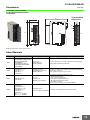
I/O Circuit
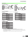
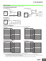
The following diagrams show the internal circuit of the analog I/O section.
Input Circuits
15 kΩ
Input (+)
15 kΩ
250 Ω
1 MΩ
15 kΩ
15 kΩ
Input (–)
Voltage/
current
input switch
AG
(analog 0 V)
Input circuit
and
conversion
circuit
1 MΩ
AG (common to all inputs)
Voltage Output Circuits
Output
switch and
conversion
circuit
Current Output Circuits
AMP
Voltage
output (+)
Voltage
output (–)
AG (common to all outputs)
Output
switch and
conversion
circuit
AMP
AMP
Current
output (+)
Current
output (–)
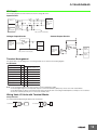
Terminal Arrangement
The signal names corresponding to the connecting terminals are as shown in the following diagram.
CJ1W-MAD42
Voltage output 2 (+)
B1
Output 2 (–)
B2
Current output 2 (+)
B3
N.C.
B4
Input 2 (+)
B5
Input 2 (–)
B6
AG
B7
Input 4 (+)
B8
Input 4 (–)
B9
Note: 1.
2.
3.
4.
A1
Voltage output 1 (+)
A2
Output 1 (–)
A3
Current output 1 (+)
A4
N.C.
A5
Input 1 (+)
A6
Input 1 (–)
A7
AG
A8
Input 3 (+)
A9
Input 3 (–)
The analog I/O numbers that can be used are set in the Data Memory (DM).
The I/O signal ranges for each input and output are set in the Data Memory (DM). They can be set in units of I/O numbers.
The AG terminal (A7, B7) is connected to the 0 V analog circuit in the Unit. Connecting shielded input lines can improve noise resistance.
The N.C. terminals (A4, B4) are not connected to internal circuit.
Wiring Vasic I/O Units with Terminal Blocks
Crimp terminals
Use crimp terminals (M3) having the dimensions shown below.
6.2 mm max.
6.2 mm max.
13