1
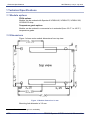
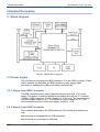
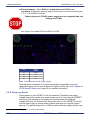
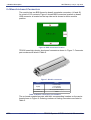
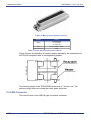
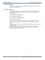
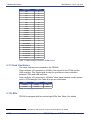
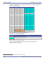
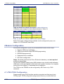
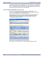
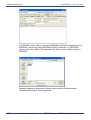
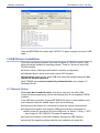
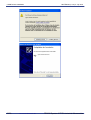
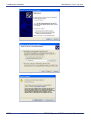
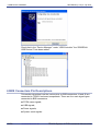
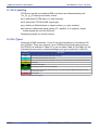
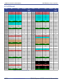
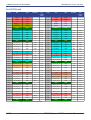
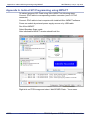
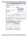
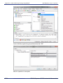
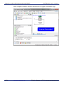
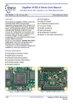
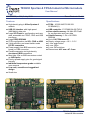
TE0630 Spartan-6 FPGA Industrial Micromodule
User Manual
UM-TE0630 (v 0.21) 3 July 2013
Trenz Electronic GmbH
Features
Specifications
● High-density plug-in Xilinx Spartan-6
module
● USB 2.0 interface with high-speed
(480 Mbit/s) data rate
● Large SPI Flash for configuration and user
data, accessible via FPGA, JTAG and USB
interfaces
● Large DDR3 SDRAM
● FPGA configuration via SPI, JTAG or USB
● 3 high-efficiency on-board switch-mode
DC-DC converters
● Power supply from B2B connector (carrier
board) or USB connector
● Flexible expansion via high-density
shockproof B2B connectors
● Most user I/Os on B2B connectors routed
as LVDS pairs
● Evenly spread supply pins for good signal
integrity
● Industrial temperature grade available
upon request
● Low-cost, versatile and ruggedized
design
● Small size
● FPGA - XC6SLX45/75/100/1502CSG484C(I)
● USB-controller: CY7C68013A-56LTXC(I)
● Non-volatile memory: 64 Mbit SPI Flash
for configuration and user data
● Volatile memory: 1 Gb x 16 DDR3
SDRAM
● Up to 110 FPGA user I/O
● Supply voltage range: 4.0 V - 5.5 V
● 1 user push-button
● 4 user LEDs
● 2 user DIP switches
● Dimensions: 40.5 mm x 47.5 mm
1/39
www.trenz-electronic.de
TE0630 Spartan-6 FPGA
Industrial Micromodule
UM-TE0630 (v 0.21) 3 July 2013
Table of Contents
1 Technical Specifications...............................................................................................................4
1.1 Module options.....................................................................................................................4
1.2 Dimensions...........................................................................................................................4
2 Detailed Description.....................................................................................................................5
2.1 Block Diagram......................................................................................................................5
2.2 Power Supply.......................................................................................................................5
2.2.1 Supply from B2B Connector.........................................................................................5
2.2.2 Supply from USB Connector.........................................................................................5
2.2.3 On-board Power Rails...................................................................................................6
2.2.4 Power-on Reset............................................................................................................7
2.3 FPGA User I/Os....................................................................................................................8
2.4 Board-to-board Connectors..................................................................................................9
2.5 USB Connector..................................................................................................................10
2.6 JTAG connector..................................................................................................................11
2.7 Serial EEPROM..................................................................................................................11
2.8 SPI Flash............................................................................................................................11
2.9 DDR3 SDRAM....................................................................................................................12
2.10 USB Controller.................................................................................................................12
2.11 Clock Oscillators...............................................................................................................13
2.12 LEDs.................................................................................................................................13
2.13 Push-Button......................................................................................................................14
2.14 DIP Switch........................................................................................................................14
2.15 Board revisions and assembly variants...........................................................................14
3 TE0300 compatibility.................................................................................................................15
3.1 Mechanical compatibility....................................................................................................15
3.2 Electrical compatibility........................................................................................................15
4 Module Configuration................................................................................................................17
4.1 JTAG FPGA Configuration.................................................................................................17
4.2 SPI FPGA Configuration.....................................................................................................18
4.3 eFUSE programming..........................................................................................................18
4.4 EZ-USB FX2 Firmware Programming................................................................................18
4.5 EZ-USB FX2 EEPROM Programming...............................................................................19
5 USB Drivers Installation.............................................................................................................21
5.1 Generic Driver....................................................................................................................21
5.2 Dedicated Driver.................................................................................................................24
6 B2B Connectors Pin Descriptions.............................................................................................26
6.1 Pin Labelling.......................................................................................................................27
6.2 Pin Types............................................................................................................................27
6.3 J4 Pin-out...........................................................................................................................28
6.4 J5 Pin-out...........................................................................................................................29
6.5 Signal Integrity Considerations..........................................................................................30
7 Related Materials and References............................................................................................30
7.1 Data Sheets........................................................................................................................30
7.2 User Guides........................................................................................................................30
8 Glossary of Abbreviations and Acronyms..................................................................................30
9 Legal Notices.............................................................................................................................31
9.1 Document Warranty............................................................................................................31
9.2 Limitation of Liability...........................................................................................................31
9.3 Copyright Notice.................................................................................................................31
2/39
www.trenz-electronic.de
TE0630 Spartan-6 FPGA Industrial Micromodule
UM-TE0630 (v 0.21) 3 July 2013
9.4 Technology Licenses..........................................................................................................32
10 Environmental Protection........................................................................................................33
10.1 REACH (Registration, Evaluation, Authorisation and Restriction of Chemicals)
Compliance Statement.............................................................................................................33
10.2 RoHS (Restriction of Hazardous Substances) compliance statement............................33
10.3 WEEE (Waste Electrical and Electronic Equipment).......................................................33
Appendix A. Indirect SPI Programming using iMPACT...............................................................35
Document Change History..........................................................................................................39
3/39
www.trenz-electronic.de
TE0630 Spartan-6 FPGA Industrial Micromodule
1 Technical Specifications
UM-TE0630 (v 0.21) 3 July 2013
1 Technical Specifications
1.1 Module options
FPGA options
Module can be ordered with Spartan-6 XC6SLX45, XC6SLX75, XC6SLX100,
XC6SLX150 chip1.
Temperature grade options
Module can be ordered in commercial or in extended (from -25 C° to +85 C°)
temperature grade.
1.2 Dimensions
Figure 1 shows main module dimensions from top view.
Figure 1: Module dimensions in mm
Mounting hole diameter is 3.2 mm.
1 Contact Trenz Electronic support for availability
4/39
www.trenz-electronic.de
TE0630 Spartan-6 FPGA Industrial Micromodule
2 Detailed Description
UM-TE0630 (v 0.21) 3 July 2013
2 Detailed Description
2.1 Block Diagram
Figure 2: TE0630 block diagram
2.2 Power Supply
The module can be powered by B2B connector J5 or the USB connector. If both
power supplies are available, the B2B connector power supply takes
precedence, disabling the USB power supply automatically.
2.2.1 Supply from B2B Connector
The B2B connector power supply requires a single nominal 5 V DC power
supply. The power is usually supplied to the module through the 5 V contacts
(5Vb2b) of B2B connector J5 (see chapter 6.4 J5 Pin-out). The recommended
minimum supply voltage is 4 V. The maximum supply voltage is 5.5 V. The
recommended maximum continuous supply current is 1.5 A.
2.2.2 Supply from USB Connector
The module is powered by the USB connector if the following conditions are
met:
● the module is equipped with an USB connector,
● the module is connected to a USB bus,
5/39
www.trenz-electronic.de
TE0630 Spartan-6 FPGA Industrial Micromodule
2 Detailed Description
UM-TE0630 (v 0.21) 3 July 2013
● no power supply is provided by B2B connectors.
In this case, other components (e.g. extension or carrier boards) may also be
powered by the corresponding 5 volt line (5V) of B2B connector J5.
2.2.3 On-board Power Rails
Three on-board voltage regulators provide the following power supply rails
needed by the components on the module:
● 1.2V, 3.0 A max
● 2.5V, 0.8 A max
● 3.3V, 3.0 A max
● 1.5V, 1.0 A max
Figure 3 show power supply diagram.
Figure 3: TE0630 Power diagram
The power rails are available for the FPGA and can be shared with a carrier
board by the corresponding lines of the B2B connectors J4 and J5. Please
note that the power consumption of the FPGA is highly dependent on the
design actually loaded. So please use a tool like Xilinx Xpower to estimate the
expected power consumption of your design.
Even if the provided voltages of the module are not used on the carrier board, it
is recommended to bypass them to ground with 10 nF - 100 nF capacitors.
FPGA I/O banks power supply
Spartan-6 architecture organizes I/Os into four I/O banks, see Table 1 for supply
voltage used for each bank.
VCCIO0 voltage can be configured in 3 ways:
● 2.5V - When resistor R103 is populated and resistor R102 is not
populated.
● 3.3V - When R103 is not populated and resistor R102 is populated.
6/39
www.trenz-electronic.de
TE0630 Spartan-6 FPGA Industrial Micromodule
2 Detailed Description
UM-TE0630 (v 0.21) 3 July 2013
● External supply - When R103 is not populated and R102 is not
populated. In this case external supply source have to be connected to pins
1, 2, 3, 4 of J4 B2B connector2.
Others options of VCCIO0 power supply are not supported and can
damage the FPGA!
See Figure 4 to locate R102 and R103 on PCB.
Figure 4: R102 and R103 location
Bank
Supply
Voltage
B0
VCCIO0
B1
1.5V
B2
3.3V
B3
3.3V
Table 1: FPGA banks VCCIO power supply
Note that some of Spartan-6 I/O types are partially compatible, so pins of
compatible types can be used as inputs for signal of other type. See “Spartan-6
FPGA SelectIO Resources” page 38 for detailed information.
2.2.4 Power-on Reset
During power-on, the /RESET line is first asserted. Thereafter, the supply
voltage supervisor monitors the power supply rail 3.3V and keeps the /RESET
line active (low) as long as the supply rail remains below the threshold
voltage(2.93 volt). An internal timer delays the return of the /RESET line to the
inactive state (high) to ensure proper system reset prior to a regular system
start-up. The typical delay time td of 200 ms starts after the supply rail has risen
2 See Spartan-6 documentation fo VCCIO power range.
7/39
www.trenz-electronic.de
TE0630 Spartan-6 FPGA Industrial Micromodule
2 Detailed Description
UM-TE0630 (v 0.21) 3 July 2013
above the threshold voltage.
Figure 5: Reset on power-on
After this delay, the /RESET line is reset (high) and the FPGA configuration can
start. When the supply rail voltage drops below the threshold voltage, the
/RESET line becomes active (low) again and stays active (low) as long as the
rail voltage remains below the threshold voltage (2.93 volt). Once the rail
voltage raises again and remains over the threshold voltage for more than the
typical delay time td of 200 ms, the /RESET line returns to the inactive state
(high) to allow a new system start-up.
2.3 FPGA User I/Os
TE0630 provides user I/O signals connected to B2B connectors J4 and J5.
There are 3 types of user I/O signals:
● Single ended;
● Differential pairs (each pair is configurable as 2 single-ended digital I/Os);
● Differential pairs, which can be used as clock inputs (each pair can be used
as usual differential pair or 2 single-ended digital I/Os).
Table 2 show user I/O count for J4 and J5.
J4
J5
Total
Single ended
12
18
30
Differential
18
16
34
Differential (clock)
4
2
6
Total
56
54
110
Table 2: User I/O count by connector
Table 3 show user I/O divided by VCCIO supply voltage.
VCCIO0
3.3V
Total
Single ended
1
29
30
Differential
18
16
34
Differential (clock)
4
2
6
Total
45
65
110
Table 3: User I/O count by VCCIO
8/39
www.trenz-electronic.de
TE0630 Spartan-6 FPGA Industrial Micromodule
2 Detailed Description
UM-TE0630 (v 0.21) 3 July 2013
2.4 Board-to-board Connectors
The module has two B2B (board-to-board) receptacle connectors (J4 and J5)
for a total of 160 contacts. Figure 6 shows B2B connectors location on board;
USB connector is located on the top side and is shown to define module
position.
Figure 6: B2B connectors location
TE0630 uses high-density shockproof connectors shown in Figure 7. Connector
part numbers are listed in Table 4.
Figure 7: Module connector
Supplier
Header
Digikey
H11113CT-ND
H11113TR-ND
H11113DKR-ND
Hirose
DF17(3.0)-80DS-0.5V(57)
Trenz Electronic
22684
Table 4: Module connectors part numbers
The on-board receptacles mate with their corresponding headers on the carrier
board shown in Figure 8. Ordering numbers of mating connectors are listed in
Table 5.
9/39
www.trenz-electronic.de
TE0630 Spartan-6 FPGA Industrial Micromodule
2 Detailed Description
UM-TE0630 (v 0.21) 3 July 2013
Figure 8: Mating (carrier board) connector
Supplier
Header
Digikey
H11148DKR-ND
H11148TR-ND
H11148CT-ND
Hirose
DF17(4.0)-80DP-0.5V(57)
Trenz Electronic
22938
Table 5: Carrier board headers part numbers.
Figure 9 shows the definition of stacking height featured by the combination of
the TE0630 receptacle with its corresponding header.
Figure 9: B2B stacking
The stacking height of the TE0630 B2B connectors is 7 (seven) mm. The
stacking height does not include the solder paste thickness.
2.5 USB Connector
The module uses a mini-USB (B type) receptacle connector.
10/39
www.trenz-electronic.de
TE0630 Spartan-6 FPGA Industrial Micromodule
2 Detailed Description
UM-TE0630 (v 0.21) 3 July 2013
Figure 10: Mini-USB connector
2.6 JTAG connector
The offset holes of header J2 allow a removable press fit of standard 0.100 inch
header pins to connect flying leads without any soldering necessary. JTAG
signals are available on the dedicated header J2 through a JTAG programmer
with flying leads as described in Table 6.
TMS
TDI
TDO
TCK
GND
Vref (2.5 V)
Table 6: JTAG header J2 pin-out
2.7 Serial EEPROM
TE0630 is equipped with a Micron Technology 24LC128 128 K I2C CMOS Serial
EEPROM (U1). It is used for EZ-USB FX2 firmware, vendor ID and device ID
storage. EEPROM is accessible through the EZ-USB FX2 microcontroller.
2.8 SPI Flash
TE0630 is equipped with a Winbond W25Q64BV 64 Mb (8 MB) serial flash
memory chip (U14). This serial flash chip can operate as general SPI memory
mode and in double or quad modes. Usage of dual and quad modes increase
bandwidth up to 40 MB/s. For more information see Winbond W25Q64BV
product owerview.
11/39
www.trenz-electronic.de
TE0630 Spartan-6 FPGA Industrial Micromodule
2 Detailed Description
UM-TE0630 (v 0.21) 3 July 2013
2.9 DDR3 SDRAM
TE0630 is equipped with a 1 Gb (128 MB) DDR3 SDRAM chip. DDR3 memory
is connected to FPGA bank 1.
2.10 USB Controller
TE0630 is equipped with a Cypress EZ-USB FX2 controller to provide a highspeed USB 2.0 interface. The controller uses 4 interfaces (See chapter 2.1
Block Diagram):
● USB interface (to USB connector);
● I2C interface (to EEPROM);
● SPI interface (to FPGA and Flash);
● FIFO interface (to FPGA).
The I2C interface connects the USB controller to the EEPROM chip, which
stores vendor ID and device ID. See chapter 2.14 DIP Switch for available
options.
The SPI interface id used to communicate with the FPGA and to access the SPI
serial Flash chip.
The FIFO interface provides a high-speed communication channel with the
FPGA. The interface can transfer up to 48 MB/s burst rate. FPGA pin-out
information can be found in Table 7.
12/39
www.trenz-electronic.de
TE0630 Spartan-6 FPGA Industrial Micromodule
2 Detailed Description
UM-TE0630 (v 0.21) 3 July 2013
Signal name
FPGA pin
FD0
J6
FD1
H8
FD2
H5
FD3
H6
FD4
G7
FD5
G8
FD6
F8
FD7
A3
24MHZ1
G3
PA0/INT0
D1
PA1/INT1
D2
PA2/SLOE
C1
PA3/WU
E4
PA4/FIFOADDR0
B1
PA5/FIFOADDR1
C3
PA6/PKTEND
B2
PA7/FLAGD/SLCS
A2
RDY1/SLWR
M3
RDY0/SLRD
M4
CTL2/FLAGC
E3
CTL1/FLAGB
E1
CTL0/FLAGA
F3
IFCLK
N4
Table 7: USB controller interface: FPGA pin-out
2.11 Clock Oscillators
Two clock oscillators are installed on the TE0630.
Clock oscillator U10 generates a 24 MHz clock signal for the FPGA and the
USB controller. This clock signal is used for synchronous communication
between FPGA and USB controller.
Clock oscillator U11 generates a 100 MHz3 clock signal used as a main system
clock in FPGA designs. See Table 8 for pin-out information.
Signal
Frequency
FPGA pin
24MHZ1
24 MHz
G3
SYSCLK
100 MHz
AA12
Table 8: Clock signals pin-out
2.12 LEDs
TE0630 is equipped with four active-high LEDs. See Table 9 for details.
3 Oscillator frequency can be changed by user request. Contact Trenz Electronic for details.
13/39
www.trenz-electronic.de
TE0630 Spartan-6 FPGA Industrial Micromodule
2 Detailed Description
UM-TE0630 (v 0.21) 3 July 2013
Signal name
FPGA pin
LED
U_LED1
F1
D3
U_LED2
F2
D5
U_LED3
J4
D6
U_LED4
K8
D7
Table 9: LEDs pin-out
2.13 Push-Button
TE0630 module is equipped with one active-high push-button (signal is set to
logical "1" when button is pressed). Table 10 show push-button connection
details.
Signal name
FPGA pin
PB
PB
R7
S5
Table 10: Push button pin-out
2.14 DIP Switch
On-board 4xDIP switch S1 used for system and user settings.
Switch 1 (S1A) is used to connect the USB controller to the I 2C serial EEPROM.
When S1A is "ON", serial I2C EEPROM is connected to the USB controller,
when switch is "OFF", the USB controller is disconnected from the EEPROM 4.
Turn S1A off when programming the USB EEPROM (storing the USB vendor ID
and device ID). This will force the USB controller to provide its default vendor ID
and device ID.
Switch 2 (S1B) is used to control DC-DC converters. When switch is "OFF",
converters are controlled by the USB controller. When switch is "ON",
converters are enabled regardless of USB controller actions. At start-up, the
USB controller switches off 1.2V, 1.5V and 2.5V power rails and starts up the
module in low-power mode. After enumeration, the USB controller firmware
switches the 1.2V, 1.5V and 2.5V power rails on, if enough current is available
from the USB bus.
Switches 3 (S1C) and 4 (S1D) can be used as user switches. Switches are
active-low. Pull-up resistors should be defined in user constrains file (UCF) to
use this switches in FPGA design. See Table 11 for details.
Signal name
FPGA pin
Switch
IO_L61_N_1
AB21
S1C
IO_L63_N_1
AA22
S1D
Table 11: DIP switch pin-out
2.15 Board revisions and assembly variants
To determine PCB revision and assembly variant from FPGA, TE0630 have
dedicated user signals, which can be read by user core.
Board revision coded in 4 bits BR[3:0]
4 Zero-resistor R90 (not populated by default) short this switch and connect EEPROM regardless of S1A position.
14/39
www.trenz-electronic.de
TE0630 Spartan-6 FPGA Industrial Micromodule
2 Detailed Description
UM-TE0630 (v 0.21) 3 July 2013
Signal name
FPGA pin
BR0
R19
BR1
V19
BR2
V20
BR3
T17
Table 12: Board revision pins
To define low (zero) level BR pin connected to ground rail, to define high (one)
level BR pin left float (open). These pins should be configured with "pullup"
option in user design.
See Table 12 for current list of board revisions.
BR3
BR2
BR1
BR0
0
0
0
0
00 Initial revision
Table 13: Board revisions
Module assembly variant encoded using AV[3:0] pins.
Signal name
FPGA pin
AV0
Y20
AV1
R15
AV2
R16
AV3
R17
Table 14: Assembly variants pins
To define low (zero) level AV pin connected to ground rail through zero resistor,
to define high (one) level AV pin left float (open). These pins should be
configured with "pullup" option in user design.
Available module assembly variants listed in Table 15.
AV3
AV2
AV1
AV0
0
0
0
0
Base assembly variant
Table 15: Module assembly variants
3 TE0300 compatibility
TE0630 module designed to be compatible with TE0300 board by main
mechanical and electrical characteristics.
3.1 Mechanical compatibility
Both modules have the same board dimensions. TE0630 mount holes and B2B
connectors locations are match with TE0300. See chapter 1.2 Dimensions for
detailed information.
TE0300 and TE0630 uses same B2B connectors types. In chapter 2.4 Boardto-board Connectors you can find B2B connectors part numbers and main
characteristics.
3.2 Electrical compatibility
TE0300 and TE0630 have similar power requirements and matched power
input pins. User signals to B2B connectors routed as differential pairs and single
15/39
www.trenz-electronic.de
TE0630 Spartan-6 FPGA Industrial Micromodule
3 TE0300 compatibility
UM-TE0630 (v 0.21) 3 July 2013
ended lines. Differences in pin types shown in Table 16, not listed signals have
same or compatible5 type.
Connector:Pin
TE0300 pin name
TE0300 Type
TE0630 pin name
TE0630 Type
J4:5
B3_L01_P
DIO
V3_IO_01
SIO
J4:7
B3_L01_N
DIO
V3_IO_02
SIO
J4:9
B3_L02_P
DIO
V3_IO_03
SIO
J4:11
B3_L02_N
DIO
V3_IO_04
SIO
J4:17
B0_L24_N
DIO
V0_IO_01
SIO
J4:19
B0_L24_P
DIO
V0_IO_01_N
DIO
J4:6
B3_L07_P
DIO
V3_IO_06
SIO
J4:8
B3_L07_N
DIO
V3_IO_07
SIO
J4:10
B3_L03_N
DIO
V3_IO_08
SIO
J4:12
B3_L03_P
DIO
V3_IO_09
SIO
J5:13
B3_L22_P
DIO
V3_IO_12
SIO
J5:15
B3_L22_N
DIO
V3_IO_13
SIO
J5:19
B3_L20_P
DIO
V3_IO_14
SIO
J5:21
B3_L20_N
DIO
V3_IO_15
SIO
J5:16
B3_L21_N
DIO
V3_IO_17
SIO
J5:18
B3_L21_P
DIO
V3_IO_18
SIO
J5:20
B3_L23_N
DIO
V3_IO_19
SIO
J5:22
B3_L23_P
DIO
V3_IO_20
SIO
J5:32
B2_L06_P
DIO
V3_IO_24
SIO
J5:34
B2_L06_N
DIO
V3_IO_25
SIO
J5:41
B2_GCLK13
CIO
V2_IO_02
SIO
J5:49
B2_GCLK_L13_N
CIO
V2_IO_24_P
DIO
J5:51
B2_GCLK_L13_P
CIO
V2_IO_24_N
DIO
Table 16: TE0300 and TE0630 pin types differences.
See Table 17 for pin types definitions.
Type
colour code
Description
DIO
Unrestricted, general-purpose differential user-I/O pin.
SIO
Unrestricted, general-purpose user-I/O pin.
CIO
Unrestricted, general-purpose differential user-I/O pin. This pin also can be used as FPGA clock input.
Table 17: TE0300 and TE0630 pin types
Most user signals to B2B connectors routed from same FPGA banks.
Differences shown in Table 18.
5 Signals routed as differential pairs can be used as single ended.
16/39
www.trenz-electronic.de
TE0630 Spartan-6 FPGA Industrial Micromodule
3 TE0300 compatibility
UM-TE0630 (v 0.21) 3 July 2013
Connector:Pin
TE0300 Bank
TE0630 Bank
J4:15
0
3
J4:36
0
3
J4:52
0
3
J5:33
2
3
J5:28
2
3
J5:30
2
3
J5:32
2
3
J5:34
2
3
J5:38
2
3
J5:40
3
2
J5:42
3
2
J5:50
3
2
J5:52
3
2
Table 18: TE0300 and TE0630 user signals I/O banks differences.
I/O Banks power supply for both modules shown in Table 19.
Bank
TE0300
TE0630
B0
VCCIO (1.2 V - 3.3 V)
VCCIO (1.2 V - 3.3 V)
B1
2.5 V
1.5 V
B2
3.3 V
3.3 V
B3
3.3 V
3.3 V
Table 19: TE0300 and TE0630 FPGA I/O banks power supply.
Bank 0 I/O supply voltage at both modules can be configured by user, see
chapter 2.2.3 On-board Power Rails.
4 Module Configuration
Full module configuration cycle (for just assembled board) include steps:
1. Generic USB driver installation
2. USB microcontroller large EEPROM programming
3. EEPROM programming
4. Dedicated driver installation
5. SPI Flash configuration
Steps 1-3 already performed at Trenz Electronic laboratory, and not required
to perform by end user.
To work with TE0630 module using USB interface user should install dedicated
USB driver, which provide API to work with main module functions, for complete
instructions see chapter 5.2 Dedicated driver installation.
The FPGA on the TE0630 can be configured by SPI Flash or by JTAG
connector.
4.1 JTAG FPGA Configuration
Programming using JTAG interface provide convenient and fast way to test
FPGA project. FPGA configuration programmed this way is volatile and lost
17/39
www.trenz-electronic.de
TE0630 Spartan-6 FPGA Industrial Micromodule
4 Module Configuration
UM-TE0630 (v 0.21) 3 July 2013
after reset or power cycle.
4.2 SPI FPGA Configuration
The bit-stream for the FPGA is stored in the SPI Flash. To use this bit-stream
source FPGA configuration option is set to “Master Serial/SPI”. See 2.8 SPI
Flash for additional information.
SPI Flash can be programmed in several ways:
● Direct programming by USB controller (usually done by Firmware Upgrade
Tool).
● Indirect SPI programming via FPGA pins, controlled by JTAG (can be done
using Xilinx iMPACT). See Appendix A. Indirect SPI Programming using
iMPACT.
● Direct SPI programming by FPGA, using an SPI core (FPGA project should
contain SPI interface core and software to work with it).
In SPI Flash mode, the FPGA’s internal oscillator generates the configuration
clock frequency. The FPGA provides this clock on its CCLK output pin, driving
the PROM’s Slave Clock input pin. The FPGA begins configuring using its
lowest frequency setting. If so specified in the configuration bitstream, the FPGA
increases the CCLK frequency to the specified setting for the remainder of the
configuration process. The maximum frequency is specified using the
ConfigRate bitstream generator option. The maximum frequency supported by
the FPGA configuration logic depends on the timing for the SPI Flash device.
For TE0630 SPI Flash PROM, use ConfigRate = 12 or lower.
This options are set graphically in Xilinx ISE Software Project Navigator by
selecting the following:
● Generate Programming File > Process Properties > Configuration Options >
Configuration Rate > 12 (or lower)
4.3 eFUSE programming
To program eFUSE at TE0630 module follow the steps below.
● Connect 2.5V power rail to 3.3V power rail. It can be done on B2B connector
see 6 B2B Connectors Pin Descriptions. Or if module connected to
baseboard, better to short power rails on baseboard.
● Program eFUSE using JTAG cable and iMPACT software.
● Disconnect 2.5V and 3.3V power rails.
4.4 EZ-USB FX2 Firmware Programming
TE0630 module supplied with already programmed FX2 firmware, so this
procedure is not needed for normal work flow. This procedure is required
only if custom firmware used or to restore firmware.
If the EEPROM has never been programmed before (virgin module) Switch 1
(S1A) can be switched to EEPROM (to "ON" state). See chapter 2.14 DIP
Switch for details. The USB microcontroller will detect an empty EEPROM and
18/39
www.trenz-electronic.de
TE0630 Spartan-6 FPGA Industrial Micromodule
4 Module Configuration
UM-TE0630 (v 0.21) 3 July 2013
will provide its default vendor ID and device ID to the USB host. If the EEPROM
has been programmed before (EEPROM not empty), S1A must be switched to
"OFF". The USB microcontroller will detect a missing EEPROM and will provide
its default vendor ID and device ID to the USB host.
4.5 EZ-USB FX2 EEPROM Programming
TE0630 module supplied with already programmed EEPROM, so this
procedure is not needed for normal work flow. This procedure is required
only if custom firmware used or to restore firmware.
First of all, check that Switch 1 (S1A) is actually switched to EEPROM. The
USB EEPROM can be programmed by opening the dedicated software
“Cypress USB Console” (double click the “CyConsole.exe” file in the
“1st_program\CyConsole” folder).
Click “Options > EZ-USB Interface” to Open EZ-USB Interface window.
19/39
www.trenz-electronic.de
TE0630 Spartan-6 FPGA Industrial Micromodule
4 Module Configuration
UM-TE0630 (v 0.21) 3 July 2013
“S EEPROM” button refers to the small EEPROM (256 bytes) whereas the “Lg
EEPROM” refers to the large EEPROM (64 KB). Press the “Lg_EEPROM”
button, select the “USB.iic” file and press the “Open” button to start writing to
EEPROM.
Upgrade progress is displayed in status window and is completed when
“Download Successful” text is displayed.
20/39
www.trenz-electronic.de
TE0630 Spartan-6 FPGA Industrial Micromodule
4 Module Configuration
UM-TE0630 (v 0.21) 3 July 2013
After that EEPROM will contain right VID/PID. To apply changes reconnect USB
cable.
5 USB Drivers Installation
To provide convenient interface from host computer to TE0630 module, USB
driver should be installed to operating system. There is 2 drivers to work with
TE0630 module:
● Generic driver, which work with default controller configuration.
● Dedicated driver, which works with custom FX2 firmware.
Generic driver used only for initial USB microcontroller programming and not
needed for normal work flow.
Most TE0630 users need to install only dedicated driver see chapter 5.2
Dedicated Driver.
5.1 Generic Driver
Most users don't need this driver, this driver used only for initial USB
microcontroller programming, which was already done for all supplied TE0630
modules.
If the USB microcontroller (Cypress EZ-ESB FX2) driver is not installed on the
host computer, then the easiest way to do it is the following:
● disconnect the module if it connected or leave the module unconnected;
● configure the module such that the USB microcontroller will provide its
default vendor ID and device ID to the USB host (i.e. Switch 1 (S1A) = "OFF"
-- see chapter 4.4 EZ-USB FX2 Firmware Programming);
● connect the module to the host computer through the USB interface;
● wait until the operating system detects new hardware and starts the
21/39
www.trenz-electronic.de
TE0630 Spartan-6 FPGA Industrial Micromodule
5 USB Drivers Installation
UM-TE0630 (v 0.21) 3 July 2013
hardware assistant;
● put Switch 1 (S1A) to "ON" (EEPROM connected to USB microcontroller);
● answer the hardware assistant questions as shown in the following example.
22/39
www.trenz-electronic.de
TE0630 Spartan-6 FPGA Industrial Micromodule
5 USB Drivers Installation
23/39
www.trenz-electronic.de
UM-TE0630 (v 0.21) 3 July 2013
TE0630 Spartan-6 FPGA Industrial Micromodule
5 USB Drivers Installation
UM-TE0630 (v 0.21) 3 July 2013
After that I2C EEPROM should be programmed with right Vendor ID / Device
ID, see chapter 4.5 EZ-USB FX2 EEPROM Programming.
5.2 Dedicated Driver
This driver used to work with modules which have DEWESoft firmware and
Vendor ID / Device ID programmed. All TE0630 modules supplied with
programmed USB controller and corresponding Vendor ID / Device ID in
EEPROM.
Before connect USB cable, check that Switch 1 (S1A) is on "ON" state (USB
controller connected to EEPROM).
Connect USB cable and wait until the operating system detects new hardware
and starts the hardware assistant and answer the hardware assistant questions
as shown in the following example.
24/39
www.trenz-electronic.de
TE0630 Spartan-6 FPGA Industrial Micromodule
5 USB Drivers Installation
25/39
www.trenz-electronic.de
UM-TE0630 (v 0.21) 3 July 2013
TE0630 Spartan-6 FPGA Industrial Micromodule
5 USB Drivers Installation
UM-TE0630 (v 0.21) 3 July 2013
Check that in the “Device Manager” under “USB-Controller” the “DEWESoft
USB Device 0” has been added.
6 B2B Connectors Pin Descriptions
This section describes how the various pins on B2B connectors J4 and J5 are
connected to TE0630 on-board components. There are four main signal types
connected to B2B connectors:
● FPGA users signals;
● USB signals;
● Power signals;
● System reset signals.
26/39
www.trenz-electronic.de
TE0630 Spartan-6 FPGA Industrial Micromodule
6 B2B Connectors Pin Descriptions
UM-TE0630 (v 0.21) 3 July 2013
6.1 Pin Labelling
FPGA user signals connected to B2B connectors are characterized by the
"Vx_IO_yy_p" naming convention, where:
● Vx defines the FPGA bank (x = bank number);
● IO defines an "FPGA to B2B" signal type;
● yy defines a differential pair or signal number (yy = pair number);
● p defines a differential signal polarity (P = positive, N = negative); single
ended signals do not have this field.
Remaining signals use custom names.
6.2 Pin Types
Most pins of B2B connectors J1 and J2 are general-purpose, user-defined I/O
pins (GPIOs). There are, however, up to 5 different functional types of pins on
the TE0630, as outlined in Table 20. In pin-out tables Table 21 and Table 22, the
individual pins are colour-coded according to pin type as defined in Table 20.
type
colour code
description
DIO
Unrestricted, general-purpose differential user-I/O pin.
SIO
Unrestricted, general-purpose user-I/O pin.
CIO
Unrestricted, general-purpose differential user-I/O pin. This pin also can be used as FPGA clock input.
USB
USB signals.
JTAG
Dedicated JTAG signals.
GND
Dedicated ground pin. All must be connected.
SYS
System signal. See the description of each pin in the user manual for additional information on the
corresponding signals.
POW
Power signals.
Table 20: TE0630 pin types
27/39
www.trenz-electronic.de
TE0630 Spartan-6 FPGA Industrial Micromodule
6 B2B Connectors Pin Descriptions
UM-TE0630 (v 0.21) 3 July 2013
6.3 J4 Pin-out
J4 pin
Net
Type
FPGA pin
Net
Length
(mm)
J4 pin
Net
Type
FPGA pin
Net
Length
(mm)
1
VCCIO0
POW
-
-
2
VCCIO0
POW
-
-
3
VCCIO0
POW
-
-
4
VCCIO0
POW
-
-
5
V3_IO_01
SIO
G6
13.30
6
V3_IO_06
SIO
C4
15.26
7
V3_IO_02
SIO
G4
11.05
8
V3_IO_07
SIO
D3
17.04
9
V3_IO_03
SIO
F5
10.46
10
V3_IO_08
SIO
E6
14.97
11
V3_IO_04
SIO
E5
10.08
12
V3_IO_09
SIO
D5
13.84
13
GND
GND
-
-
14
GND
GND
-
-
15
V3_IO_05
SIO
F7
10.16
16
V0_IO_11_P
DIO
B6
12.29
17
V0_IO_01
SIO
A4
5.16
18
V0_IO_11_N
DIO
A6
10.84
19
V0_IO_01_N
DIO
A5
5.14
20
V0_IO_12_N
DIO
A7
10.95
21
V0_IO_01_P
DIO
C5
6.84
22
V0_IO_12_P
DIO
C7
12.30
23
GND
GND
-
-
24
GND
GND
-
-
25
V0_IO_02_N
DIO
C6
7.27
26
V0_IO_13_N
DIO
A8
10.41
27
V0_IO_02_P
DIO
D6
8.16
28
V0_IO_13_P
DIO
B8
11.74
29
V0_IO_03_P
DIO
D7
7.93
30
V0_IO_14_N
DIO
A9
10.40
31
V0_IO_03_N
DIO
C8
7.21
32
V0_IO_14_P
DIO
C9
12.81
33
3.3V
POW
-
-
34
3.3V
POW
-
-
35
V0_IO_04_P
DIO
D9
9.34
36
V3_IO_10
SIO
M7
21.84
37
V0_IO_04_N
DIO
D8
10.08
38
V0_CLK_04_N
CIO
C12
12.96
39
V0_CLK_03_P
CIO
B12
6.00
40
V0_CLK_04_P
CIO
D11
13.32
41
V0_CLK_03_N
CIO
A12
05.01
42
V0_CLK_01_N
CIO
A10
10.97
43
GND
GND
-
-
44
V0_CLK_01_P
CIO
B10
11.84
45
V0_CLK_02_P
CIO
C11
7.93
46
GND
GND
-
-
47
V0_CLK_02_N
CIO
A11
10.76
48
V0_IO_15_N
DIO
A15
11.79
49
V0_IO_05_P
DIO
C13
7.20
50
V0_IO_15_P
DIO
C15
13.66
51
V0_IO_05_N
DIO
A13
6.11
52
V3_IO_11
SIO
M8
26.06
53
2.5V
POW
-
-
54
2.5V
POW
-
-
55
V0_IO_06_P
DIO
D10
12.84
56
V0_IO_16_P
DIO
B16
12.98
57
V0_IO_06_N
DIO
C10
13.09
58
V0_IO_16_N
DIO
A16
10.96
59
V0_IO_07_P
DIO
F10
16.22
60
V0_IO_17_P
DIO
C17
16.33
61
V0_IO_07_N
DIO
E10
15.43
62
V0_IO_17_N
DIO
A17
13.51
63
GND
GND
-
-
64
GND
GND
-
-
65
V0_IO_08_N
DIO
A14
8.21
66
V0_IO_18_P
DIO
B18
15.19
67
V0_IO_08_P
DIO
B14
9.11
68
V0_IO_18_N
DIO
A18
13.77
69
V0_IO_09_N
DIO
C14
9.40
70
TDI
JTAG
E18
-
71
V0_IO_09_P
DIO
D15
9.40
72
TDO
JTAG
E14
-
73
1.2V
POW
-
-
74
1.2V
POW
-
-
75
V0_IO_10_N
DIO
C16
9.65
76
TCK
JTAG
D14
-
77
V0_IO_10_P
DIO
D17
9.58
78
TMS
JTAG
E16
-
79
GND
GND
-
-
80
GND
GND
-
-
Table 21: J4 connector pin-out
28/39
www.trenz-electronic.de
TE0630 Spartan-6 FPGA Industrial Micromodule
6 B2B Connectors Pin Descriptions
UM-TE0630 (v 0.21) 3 July 2013
6.4 J5 Pin-out
J5 pin
Net
Type
FPGA pin
Net
Length
(mm)
J5 pin
Net
Type
FPGA pin
Net
Length
(mm)
1
5Vb2b
POW
-
-
2
5Vb2b
POW
-
-
3
5Vb2b
POW
-
-
4
5Vb2b
POW
-
-
5
5V
POW
-
-
6
/MR
SYS
-
-
7
B2B_D_P
USB
-
-
8
/RESET
SYS
-
-
9
B2B_D_N
USB
-
-
10
RESET
SYS
-
-
11
GND
GND
-
-
12
GND
GND
-
-
13
V3_IO_12
SIO
T2
19.97
14
V3_IO_16
SIO
U1
10.26
15
V3_IO_13
SIO
T1
18.91
16
V3_IO_17
SIO
U3
11.74
17
V2_IO_01
SIO
V15
18.18
18
V3_IO_18
SIO
V1
9.72
19
V3_IO_14
SIO
AA2
16.26
20
V3_IO_19
SIO
V2
10.03
21
V3_IO_15
SIO
AB2
15.23
22
V3_IO_20
SIO
Y1
9.21
23
GND
GND
-
-
24
GND
GND
-
-
25
V2_IO_01_N
DIO
AB6
10.68
26
V3_IO_21
SIO
Y2
8.73
27
V2_IO_01_P
DIO
AA6
12.54
28
V3_IO_22
SIO
AB3
6.68
29
V2_IO_02_P
DIO
Y7
13.32
30
V3_IO_23
SIO
Y3
8.38
31
V2_IO_02_N
DIO
AB7
11.56
32
V3_IO_24
SIO
AB4
6.65
33
V3_IO_27
SIO
U8
8.41
34
V3_IO_25
SIO
AA4
7.51
35
3.3V
POW
-
-
36
3.3V
POW
-
-
37
V2_IO_03_N
DIO
AB8
12.43
38
V3_IO_26
SIO
Y4
8.41
39
V2_IO_03_P
DIO
AA8
13.01
40
V2_IO_10_P
DIO
W6
9.20
41
V2_IO_02
SIO
AB12
12.62
42
V2_IO_10_N
DIO
Y6
8.31
43
GND
GND
-
-
44
GND
GND
-
-
45
V2_CLK_01_N
CIO
AB11
11.34
46
V2_IO_11_N
DIO
Y8
8.09
47
V2_CLK_01_P
CIO
Y11
12.64
48
V2_IO_11_P
DIO
W9
9.10
49
V2_IO_04_P
DIO
W15
14.63
50
V2_IO_12_P
DIO
Y9
8.40
51
V2_IO_04_N
DIO
Y16
12.42
52
V2_IO_12_N
DIO
AB9
6.60
53
2.5V
POW
-
-
54
2.5V
POW
-
-
55
V2_IO_05_N
DIO
U14
17.21
56
V2_CLK_02_N
CIO
AB10
7.26
57
V2_IO_05_P
DIO
T14
18.75
58
V2_CLK_02_P
CIO
AA10
8.16
59
V2_IO_06_P
DIO
AA14
12.39
60
V2_IO_13_P
DIO
W11
11.39
61
V2_IO_06_N
DIO
AB14
11.34
62
V2_IO_13_N
DIO
Y10
10.30
63
GND
GND
-
-
64
GND
GND
-
-
65
V2_IO_07_N
DIO
AB15
11.87
66
V2_IO_14_N
DIO
Y12
9.80
67
V2_IO_07_P
DIO
Y15
13.55
68
V2_IO_14_P
DIO
W12
10.80
69
V2_IO_08_P
DIO
AA16
12.61
70
V2_IO_15_P
DIO
Y13
10.20
71
V2_IO_08_N
DIO
AB16
11.72
72
V2_IO_15_N
DIO
AB13
8.40
73
1.2V
POW
-
-
74
1.2V
POW
-
-
75
V2_IO_09_N
DIO
AB18
11.91
76
V2_IO_16_N
DIO
Y14
9.72
77
V2_IO_09_P
DIO
AA18
12.57
78
V2_IO_16_P
DIO
W14
10.72
79
GND
GND
-
-
80
GND
GND
-
-
Table 22: J5 connector pin-out
29/39
www.trenz-electronic.de
TE0630 Spartan-6 FPGA Industrial Micromodule
6 B2B Connectors Pin Descriptions
UM-TE0630 (v 0.21) 3 July 2013
6.5 Signal Integrity Considerations
Traces of differential signals pairs are routed symmetrically (as symmetric
pairs).
Traces of differential signals pairs are NOT routed with equal length 6. For
applications where traces length has to be matched or timing differences have
to be compensated, Table 21 and Table 22 list the trace length of I/O signal
lines measured from FPGA balls to B2B connector pins.
Traces of differential signals pairs are routed with a differential impedance
between the two traces of 100 ohm. Single ended traces are routed with 60
ohm impedance.
An electronic version of these pin-out tables are available for download from the
Trenz Electronic support area of the web site.
7 Related Materials and References
The following documents provide supplementary information useful with this
user manual.
7.1 Data Sheets
● Winbond W25Q64BV product overview.
http://www.winbond.com.tw/hq/enu/ProductAndSales/ProductLines/FlashMe
mory/SerialFlash/W25Q64BV.htm
● Xilinx DS160: Xilinx Spartan-6 Family overview
http://www.xilinx.com/support/documentation/data_sheets/ds160.pdf
● Cypress EZ-USB FX2 Controller datasheet
http://www.cypress.com/?mpn=CY7C68013A-56LTXC
7.2 User Guides
● Xilinx UG380: Spartan-6 FPGA Configuration User Guide
http://www.xilinx.com/support/documentation/user_guides/ug380.pdf
● Xilinx UG381: Spartan-6 FPGA SelectIO Resources
http://www.xilinx.com/support/documentation/user_guides/ug381.pdf
8 Glossary of Abbreviations and Acronyms
A WARNING notice denotes a hazard. It calls attention to an operating procedure, practice, or the like that, if not correctly
performed or adhered to, could result in damage to the product or loss of important data. Do not proceed beyond a WARNING
notice until the indicated conditions are fully understood and met.
6 Difference in signal lines length is negligible for used signal frequency.
30/39
www.trenz-electronic.de
TE0630 Spartan-6 FPGA Industrial Micromodule
8 Glossary of Abbreviations and Acronyms
UM-TE0630 (v 0.21) 3 July 2013
A CAUTION notice denotes a risk. It calls attention to an operating procedure, practice, or the like that, if not correctly
performed or adhered to, could result in a fault. (undesired condition that can lead to an error) Do not proceed beyond a
CAUTION notice until the indicated conditions are fully understood and met.
API
application programming interface
B2B
board-to-board
DSP
digital signal processing; digital signal processor
EDK
Embedded Development Kit
IOB
input / output blocks; I/O blocks
IP
intellectual property
ISP
In-System Programmability
PB
push button
SDK
Software Development Kit
TE
Trenz Electronic
XPS
Xilinx Platform Studio
9 Legal Notices
9.1 Document Warranty
The material contained in this document is provided “as is” and is subject to
being changed at any time without notice. Trenz Electronic does not warrant the
accuracy and completeness of the materials in this document. Further, to the
maximum extent permitted by applicable law, Trenz Electronic disclaims all
warranties, either express or implied, with regard to this document and any
information contained herein, including but not limited to the implied warranties
of merchantability, fitness for a particular purpose or non infringement of
intellectual property. Trenz Electronic shall not be liable for errors or for
incidental or consequential damages in connection with the furnishing, use, or
performance of this document or of any information contained herein.
9.2 Limitation of Liability
In no event will Trenz Electronic, its suppliers, or other third parties mentioned in
this document be liable for any damages whatsoever (including, without
limitation, those resulting from lost profits, lost data or business interruption)
arising out of the use, inability to use, or the results of use of this document, any
documents linked to this document, or the materials or information contained at
any or all such documents. If your use of the materials or information from this
document results in the need for servicing, repair or correction of equipment or
data, you assume all costs thereof.
9.3 Copyright Notice
No part of this manual may be reproduced in any form or by any means
(including electronic storage and retrieval or translation into a foreign language)
without prior agreement and written consent from Trenz Electronic.
31/39
www.trenz-electronic.de
TE0630 Spartan-6 FPGA Industrial Micromodule
9 Legal Notices
UM-TE0630 (v 0.21) 3 July 2013
9.4 Technology Licenses
The hardware / firmware / software described in this document are furnished
under a license and may be used /modified / copied only in accordance with the
terms of such license.
32/39
www.trenz-electronic.de
TE0630 Spartan-6 FPGA Industrial Micromodule
10 Environmental Protection
UM-TE0630 (v 0.21) 3 July 2013
10 Environmental Protection
To confront directly with the responsibility toward the environment, the global
community and eventually also oneself. Such a resolution should be integral
part not only of everybody's life. Also enterprises shall be conscious of their
social responsibility and contribute to the preservation of our common living
space. That is why Trenz Electronic invests in the protection of our
Environment.
10.1 REACH (Registration, Evaluation, Authorisation and Restriction of
Chemicals) Compliance Statement
Trenz Electronic is a manufacturer and a distributor of electronic products. It is
therefore a so called downstream user in the sense of REACH. The products
we supply to you are solely non-chemical products (goods). Moreover and
under normal and reasonably foreseeable circumstances of application, the
goods supplied to you shall not release any substance. For that, Trenz
Electronic is obliged to neither register nor to provide safety data sheet.
According to present knowledge and to best of our knowledge, no SVHC
(Substances of Very High Concern) on the Candidate List are contained in our
products.
Furthermore, we will immediately and unsolicited inform our customers in
compliance with REACH - Article 33 if any substance present in our goods
(above a concentration of 0,1 % weight by weight) will be classified as SVHC by
the European Chemicals Agency (ECHA).
10.2 RoHS (Restriction of Hazardous Substances) compliance
statement
Trenz Electronic GmbH herewith declares that all its products are developed,
manufactured and distributed RoHS compliant.
10.3 WEEE (Waste Electrical and Electronic Equipment)
Information for users within the European Union in accordance with Directive
2002/96/EC of the European Parliament and of the Council of 27 January 2003
on waste electrical and electronic equipment (WEEE).
Users of electrical and electronic equipment in private households are required
not to dispose of waste electrical and electronic equipment as unsorted
municipal waste and to collect such waste electrical and electronic equipment
separately. By the 13 August 2005, Member States shall have ensured that
systems are set up allowing final holders and distributors to return waste
electrical and electronic equipment at least free of charge. Member States shall
ensure the availability and accessibility of the necessary collection facilities.
Separate collection is the precondition to ensure specific treatment and
recycling of waste electrical and electronic equipment and is necessary to
achieve the chosen level of protection of human health and the environment in
the European Union. Consumers have to actively contribute to the success of
such collection and the return of waste electrical and electronic equipment.
33/39
www.trenz-electronic.de
TE0630 Spartan-6 FPGA Industrial Micromodule
10 Environmental Protection
UM-TE0630 (v 0.21) 3 July 2013
Presence of hazardous substances in electrical and electronic equipment
results in potential effects on the environment and human health. The symbol
consisting of the crossed-out wheeled bin indicates separate collection for
waste electrical and electronic equipment.
34/39
www.trenz-electronic.de
TE0630 Spartan-6 FPGA Industrial Micromodule
Appendix A. Indirect SPI Programming using iMPACT
UM-TE0630 (v 0.21) 3 July 2013
Appendix A. Indirect SPI Programming using iMPACT
To indirect program SPI Flash using Xilinx iMPACT do following steps:
Connect JTAG cable to corresponding module connector (see 2.6 JTAG
connector).
Connect JTAG cable to host computer with installed Xilinx iMPACT software.
Power-on module by external power supply source or by USB cable.
Run Xilinx iMPACT.
Select Boundary Scan mode.
After initialization iMPACT window should look like
Right click on FPGA image and select “Add SPI/BPI Flash...” from menu.
35/39
www.trenz-electronic.de
TE0630 Spartan-6 FPGA Industrial Micromodule
Appendix A. Indirect SPI Programming using iMPACT
UM-TE0630 (v 0.21) 3 July 2013
Select mcs file to program.
Select SPI Flash type corresponding to your module type and revision.
Right click on Flash image and select “Program” from menu.
36/39
www.trenz-electronic.de
TE0630 Spartan-6 FPGA Industrial Micromodule
Appendix A. Indirect SPI Programming using iMPACT
UM-TE0630 (v 0.21) 3 July 2013
Leave default programming properties and press “OK”.
Wait for operation to complete.
37/39
www.trenz-electronic.de
TE0630 Spartan-6 FPGA Industrial Micromodule
Appendix A. Indirect SPI Programming using iMPACT
UM-TE0630 (v 0.21) 3 July 2013
After completion iMPACT window should show “Program Succeeded” sign.
38/39
www.trenz-electronic.de
TE0630 Spartan-6 FPGA Industrial Micromodule
Document Change History
UM-TE0630 (v 0.21) 3 July 2013
Document Change History
ver.
date
author
0.01
07.10.11
AIK
Release.
0.02
08.10.11
AIK
Added block diagram and few sections.
0.03
10.10.11
AIK
Added USB controller section with pin-out.
0.04
12.10.11
FDR
First general review.
0.05
13.10.11
AIK
Fixes after review. Add power diagram.
0.06
17.10.11
AIK
Add USB driver section.
0.07
17.10.11
AIK
Additions to configuration section.
0.08
16.11.11
AIK
Added module photos.
0.09
17.11.11
AIK
Net length information.
0.10
21.11.11
AIK
TE0300 compatibility information
0.11
22.11.11
AIK
Additional information to compatibility chapter
0.12
30.11.11
AIK
Added eFUSE programming section
0.13
01.12.11
AIK
Adder board revision and assembly variant chapter
0.14
20.01.12
AIK
Added pin compatibility note and manual reference.
0.15
25.01.12
AIK
Added R102 R103 location image. Added Appendix A.
0.16
16.02.12
AIK
Module options chapter
0.17
05.09.12
AIK
Fixed JTAG Vref
0.18
12.09.12
AIK
Fixed net length table
0.19
27.11.12
AIK
Fixed J4 user pin count
0.20
13.03.13
AIK
Fixed Table 7
0.21
03.07.13
AIK
Fixed pin count
39/39
description
www.trenz-electronic.de
TE0630 Spartan-6 FPGA Industrial Micromodule