1
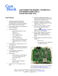
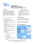
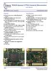
COM-1500
FPGA + DDR2 SODIMM socket + ARM + USB2
DEVELOPMENT PLATFORM
Key Features
•
•
1
Powerful digital signal processing platform
comprising:
o Large Xilinx Spartan-6 FPGA for
parallel computing:
XC6SLX45 (-A option)
XC6SLX150 (-B option)
o ARM 32-bit co-processor @120MHz
(LPC1759) for complementary
sequential computing1
o 200-pin SODIMM socket for an
optional (1 or 4 GB typ.) DDR2
memory module. 10+ Gbps throughput.
o 1Gbit NAND for non-volatile storage
of numerous FPGA configurations and
user data.
o DAC: 12-bit precision, 1 MSamples/s
for gain control
High-speed connectivity:
o Two USB 2.0 connections:
- High-speed (480 Mbps)
connection through FPGA
- Full-speed (12-Mbps)
connection through ARM
processor
o Differential LVDS connections
82 pairs (-A option)
92 pairs (-B option)
o Optional 1 or 4 port Gigabit Ethernet
and HDMI connectivity (see COM5102, COM-5401)
o Input for an external, higher-stability
10 MHz frequency reference.
•
ComScope –enabled: key internal signals
can be captured in real-time and displayed on
host computer.
DDR2 SODIMM socket is underneath.
Use of the ARM processor is at the user’s discretion.
The ARM processor is pre-programmed with all basic
functions.
MSS • 18221-A Flower Hill Way • Gaithersburg, Maryland 20879 • USA
Telephone: (240) 631-1111 Facsimile: (240) 631-1676 www.ComBlock.com
© MSS 2011 Issued 12/28/2012
Typical Applications
Multiple FPGA
configurations
+ user data
to/from
other
ComBlocks
COM-1500
+4 GB DDR2
memory
module
User I/Os
1Gb
NAND
High-throughput IP data server:
Up to 4 GB storage, 4 Gbps throughput.
COM-5401
4 * Gbps
Ethernet
USB Hub / PC
Developer port
USB Hub / PC
User port
USB
Connector
USB
Connector
120 MHz
ARM
processor
USB 2.0
PHY
74
Xilinx FPGA
XC6SLX45-2
XC6SLX150-2
external
10 MHz
frequency
reference
90
12-bit
DAC
User I/Os
The COM-1500 is interface-compatible with
numerous other ComBlock modules (RF, Analog,
Network, modem, error correction). A few
examples are illustrated below:
to/from
other
ComBlocks
64 bit wide
200-pin DDR2
SODIMM socket
Analog signal processing
Up to 4GB storage, 10+Gbps DDR2 throughput.
COM-1500 Hardware Block Diagram
USB
COM-5102
GbE +
2 HDMI
COM-1500 +
4 GB DDR2
memory
module
COM-3504
12-bit 150 MS/s
ADCs (dual)
16-bit 250 MS/s
DACs (dual)
2
2
For the latest data sheet, please refer to the ComBlock
web site: comblock.com/com1500.html.
These specifications are subject to change without
notice.
For an up-to-date list of ComBlock modules, please refer
comblock.com/product_list.html.
Nominal Operation
Supply voltage
Typical current
+4.75 to +5.25 VDC
0.5 – 1A
Use of the COM-1500 with a DDR2 SODIMM
requires an oversized power supply capable of
supplying a peak current of 2A for a very short
period (5ms). Hook-up cable should be 18AWG or
thicker to minimize voltage drop between power
supply and terminal block.
Simple Development Setup
The COM-1500 is designed to simplify the
development setup and yet allow unrestricted access
to all hardware features.
- Connect the supplied USB cable between
the COM-1500 USB development port and
a PC.
- Connect +5VDC power to the green
terminal block.
- Install the ComBlock Control Center
software on a PC for monitoring, control
and programming.
- Install the industry-standard tools for FPGA
and optional ARM development on a PC.
- Download the FPGA source code templates
from http://comblock.com/download.html Latest_FPGA_firmware
- If needed, download the ARM processor
source code template from
http://comblock.com/download.html#Latest
_ARM_firmware
Absolute Maximum Ratings
Supply voltage
98-pin connector inputs
-16V min, +16V max
-0.5V min, +3.6V max
2
The COM-1500 is compatible with a
comprehensive development environment of
industry-standard tools:
- Xilinx ISE WebPACK for development
from VHDL or Verilog source code to
FPGA binary. [free –A option only]
- Eclipse IDE + GNU ARM toolchain from
C/C++ source code to ARM binary. [free]
- ComBlock flashloader to program the
FPGA and ARM binaries into the board
non-volatile flash memory over USB.
[included]
- Optional JTAG USB pod (for ARM incircuit debugging)
Getting Started with FPGA
Development
Developing a custom FPGA-based application
requires six key steps:
1) The user writes VHDL or Verilog source
code.
2) The Xilinx synthesis tool (XST), part of the
Xilinx Integrated Software Environment
(ISE) design suite, converts the source code
into hardware primitives (.ngc file).
3) The constituent .ngc files are then mapped
into the target FPGA and net routing takes
place, again under the supervision of the
Xilinx ISE. The output is a binary .bit file.
4) The Xilinx iMPACT tool reformats the .bit
file into a .mcs PROM file.
5) The ComBlock Control Center programs
the .mcs file into the board non-volatile
(flash) memory.
6) At power-up, the ARM processor
configures the FPGA using the designated
.mcs configuration file stored on the flash
memory.
VHDL/
Verilog
source
code
FPGA
configuration
file (.mcs)
Xilinx ISE tools:
Editor
Synthesis
FPGA map
FPGA place & route
Generate .bit file
Convert to .mcs file
COM-1500
large flash
memory stores
several FPGA
configurations
FPGA
configured
ComBlock Control Center:
At power up
ARM processor
automatically
configures
FPGA
program new .mcs file
into flash memory
Development environment
COM-1500
large flash
memory stores
several FPGA
configurations
FPGA
configured
At power up
ARM processor
automatically
configures
FPGA
Run-time environment
Getting Started with ARM
Development
Writing code for the ARM co-processor is optional.
The ARM processor is factory programmed with
the full set of functions described in this document.
In many application cases, the processor could be
left as is.
However, since the processor resources are
significantly underutilized after the initial
configuration, it is made available for developers to
implement additional digital signal processing
algorithms or customize the power profile.
The ARM co-processor code template is available
for download at
www.comblock.com/download.html#Latest_ARM_
firmware
See also
http://comblock.com/howtoFPGA_VHDL.html
3
Operations
Graphical User Interface
A user-friendly graphical user interface (hereafter
named ComBlock Control Center) is supplied with
the COM-1500. The ComBlock Control Center runs
on any Windows PC (running XP or above). It
allows the user to communicate with the COM1500 over the USB 2.0 interface and when other
ComBlocks are connected, via serial link, LAN or
PCMCIA/Cardbus.
The primary use of the ComBlock Control Center is
to:
(a) Download new FPGA firmware (into nonvolatile Flash memory)
(b) Set control registers
(c) Monitor status registers
(d) Capture and display internal signals
(ComScope).
When activated, the ComBlock Control Center
enumerates the ComBlock modules within the
assembly. The modules are identified by their name
in a tree-like structure. Each module can be
configured and monitored remotely.
The ComBlock Control Center software is provided
with all ComBlock modules. The user’s manual can
be found at
www.comblock.com/download/ccchelp.pdf.
Flash Memory
The FPGA configurations are stored in the
COM-1500 non-volatile (Flash) memory. The
ComBlock Control Center includes the utility to
(re)write the FPGA .mcs PROM file into the flash
memory over USB. Upon clicking on the
button the following panel will pop-up:
4
Detailed instructions are available in the USB user
manual
www.comblock.com/download/USB20_UserManual.pdf
Accidental FPGA file corruption
The COM-1500 is protected against corruption by
an invalid FPGA configuration file. To recover
from such occurrence, connect a jumper in JP1
position 2-3 prior and during power-up. This
prevents the FPGA configuration. Once this is
done, the user can safely re-load a valid FPGA
configuration file into flash memory using the
ComBlock Control Center GUI.
Analog I/Os
From this panel, one can select the default
personality index and program the FPGA .mcs
configuration file into the board flash memory.
Instructions on how to generate a .mcs formatted
file from a Xilinx .bit file are available here:
USB
A driver must be installed prior to using USB to
communicate with ComBlocks for the first time. In
summary, connect the ComBlock to power and a
Windows OS PC via USB, then go to the Control
Panel | Device Manager and add the driver by
pointing to the driver located in the CD-ROM
/Windows Drivers/USB 2.0/Windows Driver folder.
A 14-pin header (J4) is provided for easy access to
several key analog I/Os, digital I/Os and interrupt.
GND
GND
GND
GND
TP2
TP4
GND
DAC2
PWM
ADC1
ADC2
TP1
TP3
+3.3V
14
13
The COM-1500 comprises two USB ports labeled
USB HI SPEED and DEV. The development port
(DEV) is the recommended port for flash
programming, as it does not depend on the FPGA
being properly configured. The USB high-speed
data port (HI-SPEED) could be inaccessible in the
case of an invalid FPGA configuration.
ARM Co-processor Test Points
2
1
The COM-1500 Supports multiple personalities
and dynamic reconfiguration:
• Up to 8 FPGA configurations can be stored in
non-volatile flash memory.
• The selected configuration is automatically
reloaded at power up or upon software
command within 1.2 seconds (-A) or 4 seconds
(-B).
The COM-1500 includes multiple ADCs and DACs
as listed below:
Function
Precision
Speed
Under
control by
DAC1
12-bit
1 MS/s
FPGA
DAC2
10-bit
TBD
ARM
PWM
10-bit
TBD
ARM
ADC1
12-bit
100KS/s
ARM
ADC2
12-bit
100KS/s
ARM
Power Control
The COM-1500 hardware is designed to operate in
several low-power modes:
- Sleep mode 1:
o The ARM processor is the only
powered circuit. It can be woken up by
an external wake-up signal or a USB
input pin transition (USB development
port).
o FPGA is off. It will need to be
reconfigured upon wake-up.
o DAC/DDR2 SDRAM/NAND are off.
5
-
-
Sleep mode 2:
o ARM processor is active and able to
communicate through USB.
o FPGA is in suspend mode, i.e. keeps
state and configuration.
o DAC/DDR2 SDRAM/NAND are off.
Operating:
o Individual controls for powering the
DAC, DDR2 SDRAM and NAND are
accessible through the ARM processor.
Power control requires custom programming of the
ARM processor.
Mechanical Interface
pin 3 [D+]
(1.504", 2.755")
Mounting hole
(0.160",2.840")
corner (3.000", 3.000")
USB DEV
USB HI-SPEED
port. MiniAB Data port. MiniAB
pin 1 [+5V]
(0.954", 2.500")
pin A1 (Top)
(0.000 2484.25)
J2
J1
A1
A1
5VDC Power
Terminal
Block, 90 deg
J3
Mounting hole
(2.840", 2.840")
GND +5VDC
Test points (J4)
14
1
Left connector
98-pin Straddle
Mount Connector
P/N: Sullins
NWE49DHRN-T941
J6
Top view
Right connector
98-pin Straddle
Mount Connector
P/N: Sullins
NWE49DHRN-T941
J9
•
The resulting bit file (.mcs) is ready to be
loaded into flash memory.
The sample code describes how the application
interfaces with the ComBlock Control Center
graphical user interface through control and
monitoring registers. Monitoring and control
messages and syntax are described in
www.comblock.com/download/m&c_reference.pdf.
It also describes how to capture key internal signals
in real-time and display on a host computer using
the ComScope feature of the ComBlock Control
Center. The ComScope user manual is available at
www.comblock.com/download/comscope.pdf
Finally, the code template includes the following
binary (.ngc) drivers:
• DDR2 driver
• 12-bit auxiliary DAC driver
• USB 2.0 driver
• Tri-mode 10/100/1000 Mbps Ethernet
MAC
USB 2.0 Driver
A49
A49
Mounting hole
(0.160",0.160")
J7 EXT-REF
Input external 10MHz
Corner(0.000", 0.000") SMA female,
Edge Mount
Mounting hole
(2.840", 0.160")
SMA center pin
(0.510",0.180")
Software to help developers create USB high-speed
communications between the COM-1500 platform
and a host PC is provided. The USB 2.0 software
package includes the following:
•
USB20 NGC component for integration
within the VHDL code.
•
VHDL top-level code template
•
Windows device driver (.sys, .inf files)
The board schematics are available on-line at
•
Java API, .dll and application sample code
http://comblock.com/download/com_1500schematics.pdf
•
C/C++ application sample code
Mounting hole diameter: 0.125"
Maximum height 0.500"
Schematics
VHDL code template
A VHDL template project is available on the
ComBlock CD or on-line at
http://comblock.com/download.html#COM1500template
The template project includes:
•
The VHDL source code (.vhd)
•
The constraint file (.ucf) listing all pin
assignments
•
The Xilinx ISE project with the synthesis
and implementation settings
The USB 2.0 software package is available on the
ComBlock CD and can also be downloaded from
www.comblock.com/download/usb20.zip.
The user manual is available at
www.comblock.com/download/USB20_UserManual.pdf
6
Java app.
API
C/C++
application
.dll
Clock Architecture
The clock distribution scheme embodied in the
COM-1500 is illustrated below.
Driver
ARM Cortex M3
PC Operating System
PC Hardware
USB
DLL
xK/L
120 MHz
processing
clock
DLL
xM/N
24 MHz
Crystal
USB PHY
60 MHz
low-jitter clock
External
10 MHz frequency
reference
(SMA connector)
FPGA
USB2
NGC
component
ComBlock
FPGA Development
Platform
Blue: supplied hardware
Green: supplied ready-to-use software
Yellow: source code examples
PLL
xO/P
CLK_IN
SAMPLE_CLK_IN
DATA_IN
Dual
Port
RAM
CLK_P
synchronous
processing
clock
125 MHz typ.
CLK_OUT
SAMPLE_CLK_OUT
DATA_OUT
Input clock
up to approx.
150 MHz
PLL
xQ/R
125 MHz
250 MS/s
Dual Port
RAMs
64-bit DDR
DDR2 SDRAM
SODIMM
Most of the COM-1500 internal frequencies are
locked onto a single 24 MHz crystal oscillator. This
oscillator (part of the USB PHY) serves as
reference for the 120 MHz ARM coprocessor clock,
the 60 MHz USB PHY interface clock, and the 125
MHz FPGA clocks.
The VHDL code template generates the following
FPGA clocks:
- 125 MHz processing clock
- 125 MHz DDR2 interface clock
The internal reference clock frequency stability is
typically in the range [-100, 0] ppm.
Other clock architectures and frequencies are
possible by changing the FPGA source code. For
example, in applications requiring a higher
frequency accuracy, the FPGA code can be written
to select a user-supplied ultra-stable 10 MHz
frequency signal as its frequency reference.
I/O Standards
The digital signals on connectors J6 and J9 are
LVTTL (0 – 3.3V) single-ended signals by default.
However, the I/O types can be easily changed by
7
software to other types such as differential
LVDS_33.
See Xilinx user guide ug381 for details.
Digital to Analog Converter (DAC)
A 12-bit DAC/Analog output is built-in for gain
control. The DAC operates under the direct control
of the FPGA The DAC output is connected to pin
“B13” of the J6 connector. The DAC can be
disabled in software to a high impedance state or
physically disabled by removing the 0Ω R60
resistor.
The DAC can typically operate at a 0.5V/µsec slew
rate. The output voltage range is from 0 to 3.3 V.
The driver provided in the code template allows for
approximate refresh rate of up to 1.765 MHz (slew
rate limited.)
Pinout
USB
Both USB ports are equipped with mini type AB
connectors. (G = GND). In both cases, the
COM-1500 acts as a USB device.
5V
D-
D+
ID
G
Left Connector J6
Top
CLK_IN
USER DEFINED
USER DEFINED
USER DEFINED
USER DEFINED
USER DEFINED
USER DEFINED
USER DEFINED
USER DEFINED
USER DEFINED
USER DEFINED
USER DEFINED
USER DEFINED
USER DEFINED
USER DEFINED
USER DEFINED
USER DEFINED
USER DEFINED
USER DEFINED
USER DEFINED
USER DEFINED
USER DEFINED
USER DEFINED
USER DEFINED
USER DEFINED
USER DEFINED
USER DEFINED
USER DEFINED
USER DEFINED
USER DEFINED
USER DEFINED
USER DEFINED
USER DEFINED
USER DEFINED
USER DEFINED
USER DEFINED
USER DEFINED
USER DEFINED
USER DEFINED (-B OPTION)
USER DEFINED (-B OPTION)
USER DEFINED (-B OPTION)
USER DEFINED (-B OPTION)
USER DEFINED (-B OPTION)
USER DEFINED (-B OPTION)
USER DEFINED (-B OPTION)
USER DEFINED (-B OPTION)
USER DEFINED (-B OPTION)
USER DEFINED (-B OPTION)
Bottom
A1 B1
5
10
.
.
.
.
.
.
.
.
.
.
.
15
20
25
30
35
40
45
M&C_RX
1
2
3
4
5
USER DEFINED
USER DEFINED
USER DEFINED
USER DEFINED
GND
USER DEFINED
USER DEFINED
USER DEFINED
USER DEFINED
USER DEFINED
USER DEFINED
USER DEFINED
USER DEFINED or 12-BIT DAC OUT
USER DEFINED
USER DEFINED
USER DEFINED
USER DEFINED
USER DEFINED
USER DEFINED
GND
USER DEFINED
USER DEFINED
USER DEFINED
USER DEFINED
USER DEFINED
USER DEFINED
USER DEFINED
USER DEFINED
USER DEFINED
USER DEFINED
GND
USER DEFINED
USER DEFINED
USER DEFINED
USER DEFINED
USER DEFINED
USER DEFINED
USER DEFINED
USER DEFINED
USER DEFINED (-B OPTION)
USER DEFINED (-B OPTION)
GND
USER DEFINED (-B OPTION)
USER DEFINED (-B OPTION)
USER DEFINED (-B OPTION)
USER DEFINED (-B OPTION)
USER DEFINED (-B OPTION)
USER DEFINED (-B OPTION)
M&C_TX
A49 B49
98-pin to 40-pin adapters to interface with other
Comblocks are supplied free of charge. Please let us
know about your interface requirements at the time of
order.
8
Compatibility List
Right Connector J9
Top
CLK_IN
USER DEFINED
USER DEFINED
USER DEFINED
USER DEFINED
USER DEFINED
USER DEFINED
USER DEFINED
USER DEFINED
USER DEFINED
USER DEFINED
USER DEFINED
USER DEFINED
USER DEFINED
USER DEFINED
USER DEFINED
USER DEFINED
USER DEFINED
USER DEFINED
USER DEFINED
USER DEFINED
USER DEFINED
USER DEFINED
USER DEFINED
USER DEFINED
USER DEFINED
USER DEFINED
USER DEFINED
USER DEFINED
USER DEFINED
USER DEFINED
USER DEFINED
USER DEFINED
USER DEFINED
USER DEFINED
USER DEFINED
USER DEFINED
USER DEFINED
USER DEFINED
USER DEFINED
USER DEFINED
USER DEFINED
USER DEFINED
USER DEFINED
USER DEFINED
USER DEFINED
USER DEFINED
USER DEFINED
Bottom
A1 B1
5
10
.
.
.
.
.
.
.
.
.
.
.
15
20
25
30
35
40
45
M&C_TX
USER DEFINED
USER DEFINED
USER DEFINED
USER DEFINED
GND
USER DEFINED
USER DEFINED
USER DEFINED
USER DEFINED
USER DEFINED
USER DEFINED
USER DEFINED
USER DEFINED
USER DEFINED
USER DEFINED
USER DEFINED
USER DEFINED
USER DEFINED
USER DEFINED
GND
USER DEFINED
USER DEFINED
USER DEFINED
USER DEFINED
USER DEFINED
USER DEFINED
USER DEFINED
USER DEFINED
USER DEFINED
USER DEFINED
GND
USER DEFINED
USER DEFINED
USER DEFINED
USER DEFINED
USER DEFINED
USER DEFINED
USER DEFINED
USER DEFINED
USER DEFINED
USER DEFINED
GND
USER DEFINED
USER DEFINED
USER DEFINED
USER DEFINED
USER DEFINED
USER DEFINED
M&C_RX
(Not an exhaustive list)
Compatible modules
COM-30xx RF/IF/Baseband receivers for frequencies
ranging from 0 to 3 GHz.
COM-3504 Dual Analog <-> Digital Conversions
COM-1600/1500 FPGA + ARM development platforms
COM-5102 Gigabit Ethernet + HDMI interface
COM-5401 4-port 10/100/1000 Mbps Ethernet
Transceivers
Software
COM-5401SOFT Tri-mode 10/100/1000 Mbps Ethernet
MAC, VHDL source code
ComBlock Ordering Information
COM-1500-A FPGA (Spartan-6 LX45) + DDR2
SODIMM socket + ARM coprocessor development
platform
COM-1500-B FPGA (Spartan-6 LX150) + DDR2
SODIMM socket + ARM coprocessor development
platform
ARM-USB-OCD JTAG debugger (optional)
MSS • 18221-A Flower Hill Way •
Gaithersburg, Maryland 20879 • U.S.A.
Telephone: (240) 631-1111
Facsimile: (240) 631-1676
E-mail: [email protected]
A49 B49
9