1
A:ON
SUITE MSB 1855 S. PEARL
(303) - 777 -AEON
DENVER
I
COLORADO
80210
USART
COMMUNICATIONS CARD
THE DIGITAL GROUP USART COMMUNICATioNS CARD·
Have you been waiting to interface your micro-computer to remote hardcopy terminals, or to transmit data over telephone
and communication lines? Well, your wait is over! The Digital Group adds data communication to the growing list of features
of our computer system, with the addition of a USART communications card.
.
The communications card provides the capabilities of asynchronous and synchronous data transmission with up to four
half- or full-duplex double buffered channels. Utilizing LSI programmable USART communication interface chips (8251's)
reduces the amount and complexity of processor software overhead as well as increasing communication speeds. The 8251
USART can be programmed by the CPU to operate utilizing virtually any serial data transmission technique presently in use
(including IBM Bi-sync). It does not handle SDLC. The USART chip does parallel-to-serial, serial-to-parallel data
conversions, data stream formatting, and transmits status and control information between the processor and the peripheral
device.
Each communication channel may be individually programmed for transmission rates of up to 9.6K baud (Asynchronous
Mode) or up to 56K baud (Synchronous Mode). Sync definition, async baud rates, character lengths, sync or async mode
selection, break character generation, and error detection parameters are set by the processor via a command word to an
enabled 8251 USART chip. Each 8251 also provides control inputs and outputs for modem control signals, and for those
signals used for transmitter and receiver control.
The communications card was designed to plug directly into an I/O slot in a Digital Group system, but may also be used as a
port driven card with other system configurations. The card requires +5V, and ± 12V DC for operation. Circuitry for port
addressing, data buffering to and from the CPU, and crystal-stabilized clocking is provided on the card. The card uses RS232-to-TTL level conversion chips (1489's) for interfacing modem and terminal signals; RXD, CfS, 5SR, and external sync
signal SYNDET. TTL-to-RS-232 level conversion chips (1488's) are provided for 8251 output signals; TXD, FITS, 5TR, and
internal sync signal SYNDET. One 20ma current loop transmitter circuit is provided on the card for transmitting to a TTY or
similar device.
The card uses a 4 MHz crystal, clock signal divided by two for 8251 internal clocking operations. For baud rate clocking
signals, an on-board frequency divider network, requiring no tuning, provides eight jumperable baud rate frequencies.
System Description
The communications card may be used with any of the currently available 8-bit microprocessors. The communications card
plugs directly into an available I/O bus slot (22-pin and 36-pin dual edge connectors required). Port addressing on the card
uses the port address lines on the I/O bus 22-pin connector, and is jumper selectable to any group of eight sequential port
addresses. The card uses two output ports and two input ports: one output port for command and mode instructions, one
output port for data words, and one input port each for reading status and assembled data words. Voltages of +5V and ± 12V
are provided by the I/O bus. For non-Digital Group system applications, these must be provided to the 22-pin card connector.
Connections for each channel's output and input signals are made to pins or "fingers" on the 36-pin card connactor.
Documentation provided includes a technical description of the communications card operation, assembly instructions, a
schematic and parts placement diagram, information on programming and operating the communications card, and a guide
to cabling and connections to communication devices. A list of p.ublications and reference materials is also included to
provide data communication information. The communications card's flexibility allows it to be used in practically all microcomputer data communication applications. If you have a specific application to consider and need additional information,
or have problems or questions concerning the card, we suggest'that you write or call The Digital Group.
-:1-
USART Communication Card Specifications
Card Dlmenllonl:
12" x 5.4" vertical, inGluding fingers.
System Requirements:
Power: +5V for TTL, 8251 circuit operation
±12V for RS-232 1488 line drivers
Microcomputer requirements:
Microprocessor: Digital Group system or other supplying 8 bit I/O ports
8 port address lines; group or 8 sequential port addresses used
'REA5 and WRi'fE strobe lines; 8 data to I/O lines. 8 data from I/O lines
Data Handling Capabilities:
•
•
•
•
•
•
•
Full duplex, double buffered, transmitter and receiver
Error detection - parity, overrun, and framing error
Transmitter control lines - TXRDY, TXEmpty, TxC
Receiver control line - RXRDY. Axe, SYNDET
Modem control lines - RTS, CTS, 5SR, DTR
Asynchronous transmission (DC to 9.6K baud)
5 to 8 bit character lengths
Clock rate - software selectable to 1x, 16x, 64x baud rate(1x not recommended for asynchronous receiver mode)
Break character generation - 1, 1%, 2 stop bits
False start bit detection
Synchronous transmission (DC to 56K baud)
5 to 8 bit character lengths
Internal or external character synchronization
Automatic sync character insertion
Card Features
•
•
•
•
•
•
•
Port address decoding - jumper selectable for group of 8 port addresses
Data bus buffers - input and output data lines to and from CPU buffered
Baud rate - jumper selectable for each 8251 USART utilized, 4 MHz on-board crystal used forelock base and 3
IC frequency divider
Up to four 8251's per card
RS-232 to TTL level shifters available:
4 RS-232-to-TTL lines available per USART chip
4 TTL-to-RS-232 lines available per USART chip
1 - 20m a current loop circuit available
Control lines RD. WR. C/O, CS
TXE, TXRDY, RXRDY. SYNDET available as external I/O pins or as status register bits. Allows either polled I/O
operation or interrupt:..structured operation.
-2-
Technical Description -
Communications Card
The communications card is intended to aid interfacing a micro-computer to peripheral devices such as remote CRT and
hardcopy terminals, and to format and serialize data for transmission over communication lines. The card itself plugs directly
into an available 1/0 slot of a Digital Group system, using the 1/0 bus for data and port address lines. Connection to external
peripherals or devices are made to pins on the card's 36-pin edge connector.
The card interfaces the CPU's parallel data environment with those lines required by perrpheral devices. The card also
functions to transmit and receive data, using programmable frame and character generation. Command, status, and control
logic are transmitted between the CPU and peripheral device by an 8251 USART interface chip.These logic signals include
standard modem and RS-232 level signals used for both status input and control output. Status and data information is input
to the CPU via the 1/0 data bus. Status and control signals between the peripheral and the communications card aretransferred via connections to the card's 36-pin dual edge connector. Connections to the card may be made to the peripheral
via the CPU backplane connector and adjoining cable, or may be made directly to the peripheral.
The circuitry on the communications card carries out port address decoding, buffering of data to and from the CPU,
clocking, and baud rate frequency generation. Four 8251 programmable communication interface chips communicate
between peripherals and the CPU, and transmit and receive data. TTL-to-RS-232 level shifting chips (1488's) are used far
sending RS-232 level signals. RS-232-to-TTL level shifters (1489's) convert incoming RS-232 level signals to TTL logic levels.
Port address decoding is carried out by using IC26 (74154,1 of 16 decoder), IC10 (7402, two input NOR gates), and IC25
(7442, 1 of 10 decoder). Eight port address lines are input to the communications card yielding 256 port addresses. Four port
address linE~s, (MSB-3 through MSB), are input to IC26 (74154) and ajumperon oneof74154'soutputsdesignatesagroupof
16 addressEls for the card. A jumper installed on the LSB+3 address line selects either the lower or upper group of eight from
the 16 addresses for the card. Two address lines (LSB+1, LSB+2) are input to IC25 (7442) to select one of the four 8251
USART chips on the card. An active low signal from IC26 is gated through IC17 with an active low signal from IC25 and
enables one of the 8251 s. The LSB is connected to the CIO line on each 8251 chip and determ1nes whether the information on
the data bus is a control word or a data word.
Data bus lines to and from the CPU are buffered using IC15 and IC16, and IC23 and IC24. An output strobe on pin X of the
card's 22-pin connector enables the buffers of IC23 and IC24 and passes data from the CPU to the data lines of the 8251s.
Data sent to the CPU from the data lines of the 8251s is gated through IC15 and IC16 with an input strobe accompanying a
valid card port address from IC18, and a READ strobe on pin 11 of the 1/0 bus.
Clocking on the card originates with a 4MHz crystal input to a clock dividing network of IC5, IC6, and IC9. A 2MHz clock is
input from IC6 to each 8251 and is used for internal clocking operations. This clock frequency is required to be a minimum of
4.5 times the desired baud rate for asynchronous mode transmission and 30 times a desired baud rate for synchronous mode
transmission. The network of IC5, IC6, and IC9, provides jumperable frequencies to control baud rates from 110 baud to 9600
baud. External clock sources optionally may be used in place of the frequency divider network to supply a baud rate clock to
each of the 8251's.
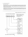
Programming the Communications Card
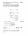
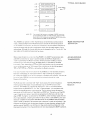
The major activity on the card occurs within the 8251 interface chips. An applications manual from one of the manufacturers
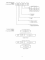
(8251 s supplied by NEC, INTEL, AMO, NATIONAL) for the 8251 is provided in the documentation. Figures 1 and 2 show the
organization of the 8251 and the flow of data between peripherals and the CPU. The 8251 USART is user-programmed to
transmit or receive data asynchronously or synchronously, at a baud rate and with a defined frame character selected by the
user. Sample programs are included which indicate programming sequences used.
The 8251 has a data bus of eight bits that receives commands and data from the CPU and sends data 8Jld status information to
the CPU via buffered 1/0 bus data lines. The card is addressed as an I/O port, using input or output instructions from the
processor to read or write data. The LSB address line, making an even orodd 1/0 address, sig~alst!,e 8251 as to whether data
or control information is being transmitted or received. An odd address (LSB 1) is used for transmitting control instructions to
the 8251, and reading a status word from the 8251. An even address is used for data input and output (LSB=O).
3-
._--------------_.
TRANSMIT
BUFFER
(P-R)
TRANSMITTER DATA
r-\\Ifffn
READ/WRITE
CONTROL
LOGIC
TRANSMIT
CONTROL
TRANSMITTER EMPTY
DATA
BUS
DATA BUS
TRANSMITTER READ'"
RESET
CLOCK
CONTROL/DAT A
WRITE DATA/CONTROL
TRANSMITTER CLOCK
READ DATA COMMAND
CHIP ENABLE'
DATA SET READY
DATA TERMINAL READY
1l
RECEIVE
BUFFER
(S-P)
MODEM
CONTROL
CLEAR TO SEND DATA
RECEIVER DATA
REQUEST TO SEND DATA
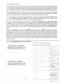
Figure 1 - The 8251 USART, programmable for synchronous or
asynchronous transmission;
double buffered internally, operates In either half or full-duplex
mode.
RECEIVER READY
RECEIVE
CONTROL
INTERNAL
DATA BUS
RECEIVER Cl.OCK
SYNC DETECT
8251 USART
TRANSMITTER DATA
TRANSMIT BUFFER
TRANSMITTER DATA
- - - - -____ PARALL EL-TO-SERIAIII-+------------l-..t
CONVERSION
(SERIAL DATA)
CHIP
ENABLE
PORT
DECODING
CIRCUITRY
OAT A/CONTROL
TRANSMITTER
I
~~_jr-------------~~---T-R-A_N-S-M-IT-T-E-R-C-L-O~C.K--~
TRANSMIT
rCONTROL
r~~;~;~:' :~~~f',-1l
READ/WRITE
CONTROL
LOGIC
CIRCUITRV
ffi
I-
~
CIJ
.~~------------.
t
DATA SET READY
~
DATA TERMINAL READY
Z w
-<
a:
I-
~--
~
MODEM
CONTROL
REOUEST TO SEND
w
CIJ
,
SYSTEM
CONTROL
I-
a:
«
w
oJ
u
~
-------~a:
RECEIVER
CONTROL
w
>
W
DATA
BUS
BUFFER
u
w
PROGRAM
-
0
>-
o
«
-
.
DATA
0«
R(AD
...
CLEAR TO SEND DATA
a:
SYNC DETECT
CIJ
::>
RECElVER CLOCK
o
z
oa:
J:
()
Z
~
I
----------------~-
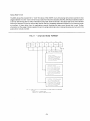
Figure 2 -
8251's implemented in a microcomputer system.
Four "handsh~g" signal lines are availab~om each 8251: two inputs, CTS (clear to send) and DSR (data set ready), and
two outputs, RTS (request to send) and DTR (data terminal ready).These signal lines are intended for modem control
applications. Of the four lines, only one, CTs, is required for the 8251 to operate. Using RS-232 input levels, a logic "0" RS232 level (+12V), must be connected to the line receiver input (1489) for each 8251 used. This "low" on the input pin of the
8251 enables the 8251 to transmit data (serial), if the TXEN bit in the command byte is set to a "1". The state of RTS andDTR
can be set ·from bits in a command word. The state of 5SR can be checked with a bit from a status read word. In a typical
application of the systeJTl (8251) with an RS-232 peripheral device or terminal, a request to send signal from the terminal
would be connected to the CTS input on the 8251, a data terminal ready signal (from peripheral) would connect to the DSR
input on the 8251. To provide the proper "handshaking" signals for a modem or peripheral device, check the literature
supplied with the device for proper sequencing and signal line connections.
Control line logic signals on the 8251 provided are RD,WR, clf), CS. The RD line is usd to read data from the CPU while the
WR signal sends data tothe CPU. The CIDline indicates to the 8251 whether data, control, or status information is on the data
bus. The CS line of each .8251 is selectively brought low by port decoding logic, so only one device is turned on at a time.
The external reset line on the 8251 is disabled and is tjed to ground. An internal reset (setting a bit in a command word) can be
used by sending a sequence of four control words (001) followed by a reset command of 100 (octal).
Assembly
To build th'3 Digital Group communication card you will need the following tools and equipment:
Fine-tipped low wattage soldering iron (approximately 25 watt)
Solder - 60/40 resin wire sold.er, 20-30 gauge
Do no" use acid core solderl
Diagonal cutters - small micro shear type preferred
Long-nosed pliers
Flux remover or alcohol
Small brush
Before mounting components on the communications card inspect the printed circuit board, comparing it to the componentside layout diagram provided. Identify the component side of the board; the Digital Group label is located on the upper-left
corner of the card. Check the areas under sockets to see that adjacent pads or traces are not shorted. Next, identify the
components that will be used on the communications card, with the parts list provided. All resistors have standard color code
markings bearing the value and tolerance of the resistors. All resistors used are 1/4 watt. Three types of capacitors are
used: ceramic disc, tantalum, and silver mica.
Ceramic disc capacitors are flat and disc-shaped and are generally identified by a ceramic casing. There is no polarity or
preferred direction. Tantalum capacitors used on this board are "tear-drop" shaped and have a value and polarity marking on
the body of the capacitor. These must be installed with the polarity indicated on the layout. The mylar capacitor used on the
card is ·rectangular-shaped, and the value marking is on the capacitor body. The voltage rating for capacitors on the parts list
is the minimum rating required; capacitors supplied in the kit may have higher voltage ratings. When soldering componf'nts
into the board make sure that your soldering iron is hot enough, is kept tinned, and is cleaned periodically with a sponge or
similar material.
Most problems that occur with newly assembled boards are related to solder shorts or "splashes", improperly soldered
connections ("cold" solder) or missed (unsoldered) pins. All IC's are socketed to avoid applying heat to "heat sensitive"IC's,
and to aid possible repair. Do not bend IC socket pins excessively before soldering as pins may break underneath the
sockets.
-5- \
If you have purchased a COMM-1 card, you will have received all components necessary for one channel. See the schematic
and layout diagram to determine placement of components.
o
Install and solder all IC sockets on the component side of the board. Sockets should be mounted as close to the
board as possible: IC's 1 through 4 require 2B-pin sockets.IC 26 requires a 24-pin socket.ICB, ICgand IC25 require
16-pin sockets. IC5, IC6, IC7 and IC's 10 through 24 require 14-pin sockets.
o
Next, install and solder R 1 - R4 in the positions indicated on the layout diagram. Use the values as indicated in the
parts list. Mount the resistors approximately 1/16 inch away from the board.
o
Install and solder 01 with the polarity indicated on the layout diagram. The Diode is installed so the card may request
wait states. While not needed with present microprocessors. this feature will accommodate faster CPUs such as the
4MHz zao .
o
Install and solder C5, CB, Cg, C11, 1 mfd tantalum capacitors in positions indicated on the layout diagram, noting
their polarity.
o
Install and solder C2, a 50 pfd silver mica capaCitor.
o
Install and solder the six .01 mfd ceramic disc capacitors, C1, C3, C4, C6, C7, and C10, in position according to the
layout diagram.
o
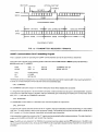
Install and solder the crystal socket in the position indicated on the layout diagram, without the crystal in the socket.
To make the crystal socket leads fit in the holes provided, cut the socket lugs as indicated below.
.
FIG. 3 - CRYSTAL SOCKET MOUNTING
o
Install the 4 MHz crystal in the crystal socket on the board.
o
Install alllC's in position, noting carefully the IC numbers on the layout diagram. Be careful not to bend any of the IC
pins under when installing the IC's.
This completes assembly of the communications card. Check over all components on the card for correct positioning, and
check over soldering. Jumpers must still be installed ~n the card for baud rates and port address selection. Also, depending
on the application of the card, jumpers or special wiring mus.t be installed. These are detailed in the operating and testing
procedure to follow.
-6-
System Planning Steps
1.
Designate ports. channels used, interface signal requirements, commands and mode instruction formats
2.
Install appropriate jumpers on the communications card
a. Baud rate jumpers for each 8251 (see Table 1)
b. Port address jumpering - IC25 and IC26 (see Table 2 and Figures 5 and 6)
c. Level shifting jumpers or modification to include 20ma current loop
d. Use of control or status signals (modem control) for "handshaking logic: RXD, CTS, DSR, DTR, RTS, TXEmpiy,
TXADY, RXADY; polling 1/0 and interrupts are accommodated by the card. CTS must be used or connected to 12V
to allow the 8251 to transmit.
--
3.
Write programming (flow charts and sample listings included)
a. Initialization routines
1) Aeset 8251 via command word - bit 06 set high
2) Write a mode instruction
3) Write sync characters if any (sync mode only)
4) Write command instruction
b. Operation routines
1) Check status word via status register read or interrupt mode processing using external 110 pins on 36-pin edge
connector (RXD, SYNDET, TXEMPTY, TXRDY, RXADY, CTS, DSA)
2) Input or output data or sync characters
3) Check status; continue transmission or reset to input new mode or command instructions
c. Program listings
4.
Cabling, diagnostic testing and operation of the communications card
1.
Designate ports, channels used, interface Signal requirements, command and mode instruction formats.
Before installing jumpers on the communications card, decide on the'application forthe card, and determine the number
of transmission channels that will be used. Aefer to the literature supplied with a particular device for specificatio~d
requi~nts of "handshaking" and interface signals~termine the modem control Signals that will be used: DTA.
Q§B, RTS,~ CTS. Modem control outputs DTR and RTS may be set via a command instruction. Modem control inputs
DSR and CTS affect bits in the 8251's status register for polled 110 operation.
The user must designate an operating mode via a mode instruction word written into the 8251's. The mode instruction
specifies sync or asynchronous operation, frame parameters, clocking rate, and error detection parameters. A command
instruction word following a mode instruction controls the actual operation of the selected format. Port addresses must
be designated for each 8251 for writing both data and control words to the 8251.
Programming the communications card requires routines to handle initialization of each transmission channel as well as
monitoring all data transmissions. Initialization routines must internally reset the 8251 USART in use, and write a mode
instruction which defines the operational characteristics of the 8251. Following the mode instruction, the processor
must send out a command instruction as well as appropriate sync characters to control the actual operation of a selected
format.
2.
Install appropriate jumpers on the communications card.
a.
Baud rate jumpering
The frequency divider network of IC5, IC6, and ICg provide connection pOints for inpLits to AXC and TXC of each 8251.
Before installing jumpers for the 8251's calculate which baud rates will be used and the baud rate factor th~1I be~
in the mode instruction. For synchronous transmission baud rate frequencies equal the clocking inputs at AXC and TXC.
For asynchronous transmission a choice is available between clock rates, 1x baud rate, 16x baud rate, 64x baud rate.
Operating at 300 baud, asynchronously, with a baud rate factor (16x baud). a jumperwould be connected to a frequency
of 4800 Hz.
-7-
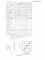
Table 1 lists calculated frequencies required .for baud rate factors. Figure 4 shows the position of the baud rate
frequencies and the connection points to TXe, RXe on each 8251.
TABLE 1 - Clock Input Required at RXC, TXC
for Selected Baud Rates
Sync Clock Input
1x Baud Rate
Baud Rate
at TXD
Async Clock Input (TXC, RXC)
64x Baud Rate
16x Baud Rate
1x Baud Rate·
110 baud
1760 Hz
150 baud
2400 Hz
9600 Hz
150 Hz
300 baud
4800 Hz
19,200 Hz
300 Hz
7040 Hz
110 Hz
600 baud
9600 Hz
38,400 Hz
600 Hz
76,800 Hz
1200 Hz
1200 baud
19,200 Hz
2400 baud
38,400 Hz
153,600 Hz
2400 Hz
4800 baud
76,800 Hz
207,200 Hz
4800 Hz
9600 baud
153,600 Hz
414,400 Hz
9600 Hz
• (1 x baud rate). Factor not recommended in asynchronous mode. Operation with 1x baud rate factor is unreliable.
-TXC. RXe CLOCK INPUT = BAUD RATE x 16 or 4800 Hz = 300 x 16.
EXAMPLE:
FIG. 4 - BAUD RATE JUMPERING,
FOR TRANSMITTER AND RECEIVER CLOCKS
0
0
0,
...
...
4
USART#1 \ 0
\'
0
0
b.
0
0
0
0
0
0
0
•• • ...
• ...
0 .....
0
153,600
76,800
38.400
19.200
9,600
4.'800
1.760
HZ'
HZ
HZ
HZ
HZ
HZ
HZ
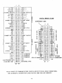
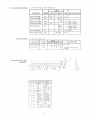
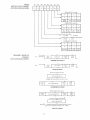
Port address selection
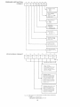
The port address example of Figures 5 and 6 shows the function of each bit of the I/O port address lines. Two jumpers
must be installed which set a designation for addressing the communications card. Shown in Figure 5 are bit settings for
addressing USART #1. USART #1 would be addressed by ports 16 & 17, USART #2 by ports 18 & 19, USART #3by20 &21,
and USART #4 by 22 & 23. See the schematic and layout diagram for jumper location.
With the port address shown, jumper 1 would be connected across the output at pin 2, which is selected output 1. Jumper
2 would be installed on the LSB + 3 address line in a non-inverting position. The LSB + 1 and LSB + 2 pOSitions control
which of the four 8251 's is enabled. The LSB pOSition selects control or data reading and writing to the 8251.
-8-
USART 11
USART 13
USART 12
USART '"
-
C/O
~
---~
CS 11
CS 13
CS #2
7432
OUTPUT SELECT JUMPER'S
I
J.4~
7442
"4"
;O.-~~
)
"8" "4"
"2"
"1"
"2"
d
"1"
.~..L
T
, MSB MSB-1 MSB~ MSB-:~
a
a
o
,..8B-
I
1
o
,.8B-211.. 8B
o
o
FIG. 5 -PORT ADDRESSING CIRCUITRY
-9-
-1 I I
L8B
/
1
TRACE RUNNING TO IC 17
IC 28
TO GATE USART SELECT SIGNAL
7.154
OUTPUT SELECTED (JUMPERS)
PORT ADDRESS 21 (OCTAL), 17 (DECIMAL)
FIG.6 - PORT SELECT JUMPERING
TABLE 2 - Valid Port Address Selection Jumpers Installed on Outputs of IC26 and IC10
Card
Port Addresses
IC10
Jumpered L
0-15
0-7
rl6-~}~==-=-~-~
IC10
Jumpered H
_..l~~~J
IC26
Output Jumpered
8 - 15
o - pin
24 - 31
1 - pin 2
1
32 - 39
40 - 47
2 - pin 3
48 - 55
56 - 63
3 - pin 4
64 - 79
64 - 71
72 - 79
4 - pin 5
80 - 95
80 - 87
88 - 95
5 - pin 6
96 - 111
96 - 103
104 - 111
6 - pin 7
112 - 127
112-119
120 - 127
7 - pin 8
32 - 47
48 - 63
\.,.tb:- 14-3
,4A-:-\5C\
(Pin 12 is GND)
1,-°:- .,.,.
240 - 255
Note:
240 - 247
248 - 255
See the schematic diagram for listing of all port pin connections.
-10-
15- pin 17
c
L~vel
Shifting Line Drivers and Line Receivers
Line drivers used on the communications card are 1488 quad line drivers, IC11, IC13, IC19, and IC21. They require
voltages of +5V, +12V and -12V to operate and convert TTL level signals to ± 12V. A logic "one" (+5V) on an input is
converted to a -12V output (RS-232 logic "one"). A logic "zero" (voltage less than .7V) input is converted to +12Voutput
(RS-232, logic "zero"). The inputs to the 1488's are connected to 8251 signals TXD, RTS, DTR, and SYNDET. Outputs of
the 1488's are brought out to the card's 36-pin dual edge connector. The pinouts of the 36-pin dual edge connector are
shown in Figure 8.
Line receivers used on the communications card are 1489quad line receivers, IC12, IC14, IC20, and IC22. They require +
5V to operate and convert incoming RS-232 signals to TTL levels required by the 8251's. The inputs (from the 36-pin
connector) to the 1489's are RXD, CTS and 5S'R. A fourth line, for external syncing in synchronous mode, may be
connected by a jumper connecting the fourth 1489 output to the SYNDET input pin on the USART chips. Jumperable
pads are provided on the communications card and are located between the chips of the top row of level shifting chips
(1488's and 1489's). These pads are also designated on the layout diagram.
t
The CTSline is of primary importance in using an 8251 for transmission. A +12V input (RS-232 logic "zero") can be tied to
pins H. 7. Z. and 22 on the card's 36-pin dual edge connector to enable the CTS line of each 8251. Alternately these pins
could be tied to the DTR line from a peripheral device. The 1489 converts the incoming +12V RS-232 level to a TTL "zero"
on the CT'S:line which is required to enable the transmitter. One 20ma transmitter is available and can be jumpered to the
transmitted output (TXD, pin 19) of any of the 8251 's as designated on the layout diagram. The jumper pads are located in
the center portion of the board. Four jumper pads correspond to the 8251 TXD lines. A jumper should be connected
between the pad at R3 and one 8251 TXD line.
NOTE FOR MORE RELIABLE OPERATION USE 8251A
-11-
r
wl1i''r'';-TXD
t\J~l.-F,HTS
Yt..l..u)Il)OTR
t .".5 YNDET OUTPUT
6u:,cA<:GND
G~\~ RXD
-..,
)
)
$'Lvf,CTS
"i' '~DSR
SYNDET INPUT
GND
T XEMPTY
TXRDY
RXRDY
SYNDET (TTL)
GND
TXD
RTS
OTR
SY NDET OUTPUT
GND
RXD
CTS
DSR
S YNDET INPUT
GND
TX EMPTY
TXRDY
RXRDY
S YNDET (TTL)
GNO
CS #1
CS '2
CS '3
CS#4
OMAT RANSMITTER
20 M A REF. GND
1
A
•
1 0
o 2 o
3 0
4 0
0 5 0
o 6 0
o 7 0
080
090
010 0
011 0
012 0
013 0
014 0
0150
0160
0170
018 0
019 0
0200
021 0
0220
0230
0240
0250
0260
0270
8280
0290
0300
0310
0320
0330
034.
0350
•
o
.360
36
l
! TXD IJJH\l(;"
I RTS 'tt ~'<"\i
~
I
(.
. OTR \('
~
"!
i'
1,s.' "
~~~~~(~
~ c.
SYNDET OUTPUT
GNDBL-~~
RXD O'Q.~'i
c
en
>
crs t:1\..VC
D S R C'..7~~_'f..t: ,\"\
:0
-t
SYNDET INPUT
....
GND
...A
TX EMPTY
TXRDY
RXRDY
SYNDET (TTL)
GND
TXD
RTS
DTR
SYNDET OUTPUT
GND
RXD
CTS
DSR
SYNDET INPUT
GND
TXEMPTY
TXRDY
RXRDY
SYNDET (TTL)
GND
C/O (COMMON)
RD (COMMON)
WR (COMMON)
N/C
N/C
EXTERNAL SYNC
.-.~
DIGIT Al GROUP 110 BUS
COMPONENT SIDE
~
+5V
GND
:J
~SB
MSB-1
MSB-2
0
MSB-3
~
LSB+3
<
~
< LSB+2
C
c
LSB+1
CJ)
LS
>
:0
INPUT STROBE
-t
MSB-7
....
en
CN
MSB-6
en
UJ
MSB-5
a:
O(/)
MSB-4
Ow
cC z MSB-3
~MSB-2
a:...I
0
MSB-1
a..
MSB
NMI
C PU-I/O UNDEFINED
+12V
Q.
(.)
1
A
0
1 0
o 2
3 0
o ~ 0
.50
.60
•
•
• 7 0
080
o 9 0
.10 0
011 0
012 0
.130
0140
0150
0160
0170
.180
0190
0200
.210
0220
22
+5V
-5V
MSB
MSB-1
MSB-2
MSB-3
LSB+3
LSB+2
LSB+1
LSB
SPARE
LSB
LSB+1
LSB+2
LSB+3
LSB+4
LSB+5
LSBtS
LSB+7
OUTPUT
CPU-I/O
-12V
0
>
-t
>
'11
:D
0
~
0
""0
c
""0
0
:0
.-4
->
Ze
me
0>:0
m
,(I)
(JJ
STROBE
UNDEFINED
Z
~
F1G. 8- PINOUT OF COMMUNICATIONS CARD 36 AND 22 PIN DUAL EDGE CONNECTORS.
SEE SCHEMATIC DIAGRAM FOR LOGIC (ACTIVE HIGH AND LOW SIGNALS),
-12- .
d.
Control and Status Instructions
Mode Instruction Formats
Following a reset operation, a mode instruction is written into the 8251. The figure below, with a segment from the 8251
applications manual, shows the instruction format that is used and gives an example mode instruction for asynchronous
transmission. Synchronous transmission is selected by setting bits DO ~nd D1 low. See the applications manual for
synchronous transmission applications.
~o~struction
of 376 (octal) illustrates how the 8251 mode may be set. Baud rate factors designate clock inputs at
TXC, RXC required for asynchronous transmission; 1x baud rate, 16x baud rate, 64x baud rate. In synchronous mode
the clock rate is equal to the baud rate (1x baud rate). The'1 x baud rate factor for asynchronous transmissions is not
recommended as it may not work reliably.
MODE INSTRUCTION OF 376 (OCTAL)
FIEID4
FIEl [) :l
FIEL[) 1
MODE instruction async, 2 stop bits
parity even, 8-bit character word, baud
rate factor: 16 x baud rate
or the transmitter clock frequency
is the baud rate x 16
BAUD RATE
-_. _._.--
--
OO--SYNCHRONOUS MODE
01-ASYNCHRONOUS 1x
10-ASYNCHRONOUS (1/16) x
11--ASYNCHRONOUS (1/64)
CHARACTER LENGTH
00-5
01-6
10-7
11-8
BITS
BITS
BITS
BITS
·1ro------
I
,;
PARITY CONTROL
--
XO-NO PARITY
01-000 PARITY
11-EVEN PARITY
FRAMING CONTROL
----------------........s!!"
OO-NOT VALID
01 NeT o;l:,lIB j
10-1 'f> STOP BITS
11-2 STOP BITS
5fOv KIT>
YES
SYNC CONTROL
XO-INTERNAL SYNC
L--------------------~_1 Xl-EXTERNAL SYNC
OX-DOUBLE SYNC CHARACTER'
l
llX-SINGLE-SY:~TER 1
FIG. 9- MODE INSTRUCTION FORMAT
-13-
Command Instruction Format
1110 command Instruction controls .trw actual operation of a 3eloctod format, and is written Into the 8251's after a mode
instruction has been programmed. Once the mode instruction has been written in the 8251, all further control "writes"
(C/O::. 1) will load the command instruction. A reset operation (internal for application of the card) will return the 8251 to
the mode instruction format. Figure 10, from the 8251 applications manual, illustrates the command instruction format.
An example command instruction of 001 (octal), written into the 8251, sets the TXEN bit (~O) "high" which enables the
transmitter. To change a command, it is necessary to write another command word (C/O = 1) intothe 8251. The mode will
remain unchanged (sync-async) until another reset and mode instruction sequence is initiated.
1 he TXO output remains "high" (marking) until the TXEN bit in the command register is enabled and the CTS line goes
"low", Data is shifted o~n ~alling edge of TXC .in the synchronous mode and in the asynchronous mode on the
falling edge of TXC at TXC, TXC/16 or TXC/64, as defined by the mode instruction.
Setting bits 01 and D'5 (OTR and RTS) "high" forces "low" the OTR and RT~tput pins on the 8251. T~e IinellLe
generally used for modern "handshaking" lines. Two input pins on the 8251 OSR and CTS complement OTR and RTS.
The DSR input signal can be tested by the CPU using a status read to test modem conditions such as data set ready. The
CTS line enables the 8251 to transmit data (along with TXEN) and must be set accordingly, The 1489's (quad line
receivers) convert RS-232 inputs to TTL levels. The 1488's (quad line drivers) convert TTL output levels to RS-232 level
signals.
A command of 044~bles the receiver and sets RTS low (request to send). The RTS line could be connected to a
transmitting device CTS line. The external pin CTS on the 8251 does not affect its operation as a receiver. A falling edge
at RXD signals the possible beginning of a START bit and new character. Input bits are sampled at the RXD pin with the
edge of AXC. The 8251 begins assembling a data character, and after a valid stop bit is encountered, loads the input
character into the parallel data bus buffer. The AXADY line is then set "high" to indicate to the processor a character is
ready to be fetched. Parity framing errors will be indicated in the status register and may be checked during a status read
operation. If the processor fails to fetch a character before a new one is assembled, an overrun flag is set and is indicated
in the status register.
F1G. 10- COMMAND INSTRUCTION FORMAT
I I
III
001 (OCTAL)
-TRANSMIT
IH
1
111
:;
I
I H
I"HH~ I
fl.!
I
{)TH 11 ,I N
L
1 HAN'.MII I NI\Bl [
1
t'rl,d,lt-'
()
{Ihdldt,
1/1\ III I l HMlhJIIL
HLAOY
111'11,' 11\1.11 " " ' "
I)UlplIl
iJTR
III /PIO
HE:CfIV( ~NABLE
en.d Ill'
I
(il>.itJlp
0
:.E
N[l
un!' AK
CHAHAl rFH
1 IOl<e5 1 AU "low "
044 (OCTAL) -RECEIVE
,)
1010111010[110101
'------
.
efl.ftoMi
I
II
Il( II III
f)~H'r ,J1'on
Hl ~,l T
~''''I III
."'1 (II
t 1,1l1~
Pf,OE)Fe.
fll.'JIJfS11US~N[J
po
11I·II,"v,IIlt,,".crn
IlOl!plll
III
LCH.J
tKtt f ll'/oiA-L II.Jse..r
t\1~~ ~tI.'~,1 fl'
!'vl.Hit' Ifl':tIIULtIOl1 Formdl
-14-
E.
1
N I [I{ HliNT MODf
t:1\.d,\t:
CthHdLrcr~
~1·\IIt.h
for Sync
Status Read Format
The 8251 allows the programmer to "read" the status of the USART at any time during its functional operation (chip
sel2.ct enabled), A normal "read"command (input data from liD port) is issued by the CPU, with the port address (state of
CIO line) determining data or status information being read, Some of the bits in the status read format have identical
meaning to external liD pins so that the 8251 can be used in a completely polled environment or in an interrupt driven
environment. A figure taken from the applications manual illustrates the status word format that is used. Further
information on the usage of status register bits and on using external pins in an interrupt structure can be found in the
applications manual provided.
FIG. 11 - STATUS READ FORMAT
U,
1\;
UI J
1)4
1)\
I):,
Fl
Of
I'E
hE
Do
()1
I I I I I I I I LCDI
USH
$VN""
H.ROY
f,nOy
1 1
I 1
SI\M[ tJU INI T IONS I\S 1/0 f'INS
1'1\1(1 I Y I IIIII)I!
111,· I't 11.1<1" ,,,I will'"'' p.lllly
II I~ ft~~el by'
tilt' ( H lHI
ttl!' CtHlIfndlld
11I',I/IICllull Pf dot'S 1101 Inhd,lt
Plltl, I~ dl~'t'ctPcl
I"
Illh'l .lflllll 01
1111'
[::I()
1
I)VI~HlnIN
llU!OH
11"'(11 ","1 ,,'.1'1 wl"'lIlh"(,l'iJ
litH''. IH,! 11',111 ,Il h.II.lLH"
Ilt~llJlt'
,ill' 11\')1:.\ lIlll' IH'IIHnps
dV,Hldhle.
(',,"lIn,dld 1Il',flll( tltlll
OE. duns
not IIllH11i1 01'1'1.111011 of lh4' H:)~J1,
llil\IVI'VI'I, 1111' IHt'VIIII".ly 'lVI" I 111\
I h,lloIt It"
1\
III'"
f IU\MII~(, 11l11tlH II\,y.ll: ollly)
1 lit· • t 11,111'\
'>f.!1 wlH'1I I v.dld
~-;I(JP lIlt I', nfll dt'leCled .It
t'/Hi of t've!y (hdl.ll It!.
Ifw
II IS IC"'t.'t
I 'y Ihe l H I." "I .hl' C')fnmoilld
III .... l1\1l I l t l l l
r E:
dl)f)\
n(ll !llhlt,!,
Ihl' I1Pt'ldIHHI til "IP H}~}l
N".~
(i)
r.ROY \'.1111,1>11 "nol IOI.,tly equlvalenl 10 Ihe TxRDY outpUI p.n, Ihe relallonsh,p
T ,nov ipIIl 1!,)
Oil Hull,', I mplV - C r~
-15-
- T,Fn
'Two sample programs have been written and may be~d as operating routines for the communications card. One is used for
transmitting data. the other for receiving data. The CTS line must be connected to a logic "0" source. The flowchart below
shows the sequence of programming steps carried out for either synchronous or asynchronous modes. Figure 12 shows
transmitting and receiver data formats for both operating modes. The choice of either mode depends directly on the
application; Asynchronous transmission is used generally with man-machine interfaces while synchronous transmission
offers higher speeds for machine-machine communication.
Both sample programs use the same reset operation sequence when initially addressing the USART. The user should consult
the applications manual for the 8251 USART,particularly the section on initiating software reset.
POWER UP
INITIALIZATION
. _____ J....
SET
MODE
/
..., .
YES
<ASYNCHRONOU~~------,
:1""'...
[
l
-~-O;;
i
i
FIRST SYNC
CHARACTER
...
-
.- .. -~
YES
YES
YES
TYPICAL PROGRAMMING FLOWCHART
-16-
AFTER POWER -UP R~SET
IDLE STATE
MARK _
1 llII
SPACE
I·
lt
OPTIONAL PARITY BIT
START BIT
DATA BITS
STOP BITS
.. I
I I I I I I: I
FRAME
~. ~ ~:
III I
II
·1·
·1
ASYNCHRONOUS TIMING
DATA BITS
-
........-
SYNC CHARACTER -
...........
DATA BITS - -.........
MARK
SPACE __~__~~~__4 -__~__6-~~__~~__~~~~~~______~__~~A-~~
-
FRAME ----..,~.....- - - - FRAME - -.....1IIoi1
FRAME
SYNCHRONOUS TIMING
FIG. 12- TRANSMITTERI RECEIVER FORMATS
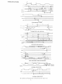
USART Communications Card Transmitting Program
This is a sample routine for operating the USART communications card as an asynchronous transmitter.
This routino uses a Digital Group operating system with subroutines HOME ERASE at 000346 (octal), KEYBOARD at
001250 (octal) and TV at 000372.
PORT
DPORT
EOU
EOU
CALL
LD
CALL
HOME ERASE
C, PORT
INITIALIZE
17
16
COMMAND DB 001
MODE DB 376
Decimal
Decimal
*INITIALIZE carries out a sequence of "out" instructions to the control port which resets the 8251. After resetting the 8251 #1,
it sends out a mode instruction which sets the format for transmitted data.
CALL COMMAND
The COMMAND subroutine outputs a command instruction word which enables the transmitter.
To change the mode operation or to send another command, a reset command must be given to the enabled 8251. Once the
mode instruction has been written to the 8251, and sync characters (sync mode only) are inserted, all "control writes" to the
8251 (C/O = 1) will load the COMMAND instruction.
CALL KEYBOARD
The KEYBOARD routine waits for a character input from the keyboard or input device.
CALL DATA OUT
The DATA OUT routine saves the contents of the "A" register (the input character) and saves all CPU flags. It does a status
read (C/O = 1) which checks to see that the transmitter is ready. This condition will only be true if the data bus buffer of the
8251 is empty, or if the last character transmitted had actually been transmitted.
If the transmitter is ready, the contents of the "C" register are decremented to effect a data port address. The data character is
writen out to the 8251 and the 8251 will transmit the character. :
Note: The 8251 will only transmit if the TXEN bit of a command word is enabled, and the CTS external pin of the 8251 is set
low. In the event that neither is true, the status line TXRDY would not go high to request another character to be input from the
processo~
-17-
TRANSMITTER ROUTINE
THIS ROUTINE EXECUTES AT (OCTAL)
066341
066341
066344
066344
066344
066344
066346
066351
066351
066351
066354
066354
066357
066357
066357
066361
066364
066364
066367
066367
066371
066373
066373
066373
066375
066377
067001
067003
067005
067005
067007
067012
067012
067014
067015
067020
067020
067020
067022
067023
067024
067024
067024
067024
067026
067026
067030
067032
067032
067033
067033
067034
067034
067036
067036
067037
001
067040
067040
376
067041
067041
315 346 000
016 021
315 371 066
315 015 067
315 250 001
016 021
315 023 067
315 372 000
030 363
076 001
355
355
355
355
076
171
171
171
171
100
355 171
072 040 067
355 171
311
072 037 067
355 171
311
365
355 170
313 107
050 372
361
015
355 171
311
0100
0110
0120
0130
0140
0150
0160
0170
0180
0190
0200
0210
0220
0230
0240
0250
0260
0270
0280
0290
0300
0310
0320
0330
0340
0350
0360
0370
0380
0390
0400
0410
0420
0430
0440
0450
0460
0470
0480
0490
0500
0510
0520
0530
0540
0550
0560
0570
0580
0590
0600
0610
0620
0630
0640
0650
* THIS IS A SAMPLE OUTPUT ROUTINE FOR DG-0022-A
CALL 346
* CALL HOME ERASE
PORT
EQU
17D
* THIS ADDRESS IS THE CONTROL PORT ADDRESS
LD C,PORT
CALL INIT
* THIS STATEMENT CALLS THE INITIALIZE ROUTINE
* INIT ALSO SENDS THE MODE WORD TO THE 8251
CALL COMAND
* THIS STATEMENT SENDS A COMAND WORD TO THE 8251
IN
CALL 1250
* IN GETS A CHARACTER FROM THE KEYBOARD AND TRANSMITS
* IT TO THE 8251 DATA PORT
LD C,PORT
CALL DATAO
* DATAO IS THE TRANSMIT ROUTINE
CALL 372
* PRINTS CHARACTER ON TV MONITOR
JR
IN
INIT LD A 001
* 001 OCTAL IS AN INVALID MODE INSTRUCTION THIS CAUSES
* THE 8251 LOOK FOR ANOTHER MODE INSTRUCTION.
OUT (C),A
OUT {C),A
OUT (C),A
OUT (C),A
LD A 100
* 100 OCTAL IS A RESET COMAND
OUT (C),A
LD A,(MODE)
* MODE IS THE MODE INSTRUCTION WORD
OUT ( C) ,A
RET
COMAND LD A,(COMND)
* COMAND IS THE COMAND WORD OUTPUT ROUTINE
* COMND IS THE COMAND INSTRUCTION WORD
OUT (C),A
RET
DATAO PUSH AF
* SAVE THE CONTENTS OF A REGISTER
* DATAO CHECKS THE STATUS OF THE 8251 FOR TXRDY THEN
* LOADS IN THE DATA CHARACTER
STATO IN
(C),A
* READ STATUS WORD
BIT O,A
JR Z,STATO
* CHECK FOR A 1 IN BIT 0 OF STATUS WORD
POP AF
* RECALL DATA CHARACTER IN A REGISTER
DEC C
* CHANGE FROM THE COMAND ADDRESS TO THE DATA ADDRESS
OUT (C),A
* OUTPUT THE DATA CHARACTER
RET
COMND DB 001
0660 * COMAND WORD (ENABLE TRANSMITTER)
0670 MODE DB 376
U680 * MODE INSTRUCTION ASYNC~ 2 STOP BITS, PARITY EVEN,
0690 * 8 BIT WORD, BAUD RATE uIVIDED BY 16
-18-
TRANSMITTER ROUTINE
THIS ROUTINE EXECUTES AT (OCTAL)
066341
066341
066344
066344
066344
066344
066346
066351
066351
066351
066354
066354
066357
066357
066357
066361
066364
066364
066367
066367
066371
066373
066373
066373
066375
066377
067001
067003
067005
067005
067007
067012
067012
067014
067015
067020
067020
067020
067022
067023
067024
067024
067024
067024
067026
067026
067030
067032
067032
067033
067033
067034
067034
067036
067036
067037
001
067040
067040
376
067041
067041
315 346 000
016 0-21
315 371 066
315 015 067
315 250 001
016 021
315 023 067
315 372 000
030 363
076 001
355
355
355
355
076
171
171
171
171
100
355 171
072 040 067
355 171
311
072 037 067
355 171
311
365
355 170
313 107
050 372
361
015
355 171
311
0100
0110
0120
0130
0140
0150
0160
0170
0180
0190
0200
0210
0220
0230
0240
0250
0260
0270
0280
0290
0300
0310
0320
0330
0340
0350
0360
0370
0380
0390
0400
0410
0420
0430
0440
0450
0460
0470
0480
0490
0500
0510
0520
0530
0540
0550
0560
0570
0580
0590
0600
0610
0620
0630
0640
0650
* THIS IS A SAMPLE. OUTPUT ROUTINE FOR DG-0022-A
CALL 346
* CALL HOME ERASE
PORT
EQU
17D
* THIS ADDRESS IS THE CONTROL PORT ADDRESS
LD C,PORT
CALL INIT
* THIS STATEMENT CALLS THE INITIALIZE ROUTINE
* INIT ALSO SENDS THE MODE WORD TO THE 8251
CALL COMAND
* THIS STATEMENT SENDS A COMAND WORD TO THE 8251
IN
CALL 1250
* IN GETS A CHARACTER FROM THE KEYBOARD AND TRANSMITS
* IT TO THE 8251 DATA PORT
LD C,PORT
CALL DATAO
* DATAO IS THE TRANSMIT ROUTINE
CALL 372
* PRINTS CHARACTER ON TV MONITOR
JR
IN
INIT LD A 001
* 001 OCTAL IS AN INVALID MODE INSTRUCTION THIS CAUSES
* THE 8251 LOOK FOR ANOTHER MODE INSTRUCTION.
OUT (C),A
OUT (C),A
OUT (C),A
OUT (C),A
LD A 100
* 100 OCTAL IS A RESET COMAND
OUT (C),A
LD A,(MODE)
* MODE IS THE MODE INSTRUCTION WORD
OUT (C),A
RET
COMAND LD A,{COMND)
* COMAND IS THE COMAND WORD OUTPUT ROUTINE
* COMND IS THE COMAND INSTRUCTION WORD
OUT (C),A
RET
DATAO PUSH AF
* SAVE THE CONTENTS OF A REGISTER
* DATAO CHECKS THE STATUS OF THE 8251 FOR TXRDY THEN
* LOADS IN THE DATA CHARACTER
STATO IN {C),A
* READ STATUS WORD
BIT O,A
JR Z,STATO
* CHECK FOR A 1 IN BIT 0 OF STATUS WORD
POP AF
* RECALL DATA CHARACTER IN A REGISTER
DEC C
* CHANGE FROM THE COMAND ADDRESS TO THE DATA ADDRESS
OUT (C),A
* OUTPUT THE DATA CHARACTER
RET
COMND DB 001
0660 * COMAND WORD (ENABLE TRANSMITTER)
0670 MODE DB 376
U680 * MODE INSTRUCTION ASYNC~ 2 STOP BITS, PARITY EVEN,
0690 * 8 BIT WORD, BAUD RATE uIVIDED BY 16
-18-
USART Communications Card Receiving Program
This is a sample routine for operating the USART communication card as an asynchronous receiver. It uses USART #1 (8251)
and ports 16 and 17 for control and data, and reading and writing to the 8251. The "C" register is used for storing the port
address used to address the USART.
This routine uses a Digital Group operating system with subroutines HOME ERASE and TV.
The subroutine IN ITIALIZE carries out a sequence of "out" instructions to the control port address which resets the 8251.
After resetting 8251 #1, it sends out a mode instruction which sets the format for transmitted or received data. A mode
instruction for setting up the 8251 for transmitting may be the same as that for receiving.
CAl.l. COMMAND
The COMMAND subroutine outputs a c~and instruction word which sets bit 5 and bit 2 high (octal 044).Bit 5, RTS, is set
high (enabled) and sets the external pin RTS of the 8251 low. The receiver enable bit (02) is also set high to allow the receiver
to collect serial data and assemble data words.
After enabling the receiver the program monitors transmissions by reading the status word of the enabled 8251. If data has
been sent correctly according to the format set up, the RXRDY bit in the staus word will be set high indicating the 8251 has an
assembled character for the microprocessor. The port address is then changed to read data (C/O = 0) and the processor
reads data from the I/O port data lines.
RECEIVER ROUTINE
0000 * THIS IS A SAMPLE INPUT ROUTINE
062242 315 346 000
0100
CALL 346
062245
0105 * CALL HOME ERASE
062242
062245
062245
062245 016 021
062247 315 267
062252
062L52 315 313
062255
062255 016 021
062257 315 323
062262 315 372
062265 030 366
062267 076 001
062271 355 171
062273 355 171
062275 355 171
062277 355 171
062301 076 100
062303 355 171
062305 072 322
062310 355 171
062312 311
062313 072 321
062316 355 171
062320 311
062321
045
062322
376
062323
062323 355 170
062325 313 117
062327 050 372
062331 015
062332 355 170
062334 366 200
062336 311
062
062
062
000
062
062
0110
0111
0120
0130
0133
0140
0150
0160
0170
0180
0190
0200
0210
0220
0230
- 0240
,0250
0260
0270
0280
0290
0300
0310
0320
0330
PORT
EQU
170
* THIS IS THE CONTROL PORT ADDRESS
LD
C,PORT
START CALL INIT
* CALL THE INITIALIZE ROUTINE
CALL COMAND
IN
EQU $
LD
C,PORT
CALL DATAl
CALL 372
JR
IN
INIT
LD
A 001
OUT (C) , A
OUT (C),A
OUT (C),A
OUT (C),A
LD
A,lOO
OUT (C),A
LD A,(MODE)
OUT (C),A
RET
COMAND LD
AJ(COMND)
OUT (l.,),A
RET
COMND DB
37D
0340 MODE
DB
0350 DATAl
0360 STATI
0370
0380
0390
0400
0410
0420
$
~2U A,
(C)
-19-
376
BIT 1,A
Z,STATI
JR
DEC C
IN A, (C)
OR 200
RET
Cabling
Figure 8 shows the pinout of the 36 and 22 pin dual edge connector of the communications card. Pins A through S of the 36
pin connector are a block of pins designated for making connection to USART #1. Pins 1 through 15 are designated for
USART #2. pins T through J for USART #3. and pins 16 through 30 designated for USART #4. Connections are only made for
those pins necessary for interfacing and may be soldered or made with "molex" type connectors.
R'S-232 connections are usually made with 25 pin "0" connectors. The typical pinout of a "0" connector is shown
below.
Pin
Function
1--------Protective ground
2--------Transmitted datR-output
3--------Received data- Input
4--------Request to Send-output
S--------Clear To Send-input
6--------0ata Set Ready-input
7--------Signal ground(common return)
20-------0ata Terminal Ready-output
For applications where cable lengths needed is less than 50 feet.or more than 50 feet but at a baud rate of roughly 300 baud or
less, the cable used is not critical and need not be shielded. In most cases, it should be use stranded wire,but solid conductors
. will probably work for short distances. Large diameter wire is not necessary since the devices are not carrying higp currents.
Connecting the outputs and their corresponding inputs is accomplished by crossing pairs of wires in the cable itself. E.G.
Pin 1
2 (TXO)
3 (RXO)
4 (RTS)
S (CTS)
6 (OSR)
Pin 7
Pin 20 (OTR)
Pin
Pin
Pin
Pin
Pin
_ _ _ _ _ _ _ 'Pin 1
----------.---------------------
Pin
Pin
Pin
Pin
Pin
- - - - - - - Pin
- - - - - - - Pin
aLAC~~
3 (RXO) WH ITE
2 (TXO) C~'RP~N
S (CTS) l~l l~~~iL,
4 (RTS) St.\)"
t
20 (OTR) "
,
7 (GNO) 13L.~C.\4
6 (OSR) YEL\J)¥J
t
.
J'
Diagnostic testing and operation of the communications card
The equipment used to test the communications card should use a voltmeter, an oscilloscope, and a frequency counter if
available.
Voltage checks can be made at the following pins:
Check for 5V:
Check for GNO at:
Pins 2,3,10 of Ie 5
Pins 2,3,10 of Ie 6
Pin 7 of Ie 7
Pins 8,10,and 14 of Ie 8
Pins 1.8,14 of IC 9
Pin S,IC S
Pin S,IC 6
Pin 14,IC 7
Pins 2,9,15,and 16 of IC 8
Pins 5,9,10,1S,and 16 of IC 9
Pins on the card's 22 pin connector can also be checked:
Pins 1,A at +SV
Pin 2 at Gnd
Pin 22 at +12V
Pin Z at -12V
-20-
Clock circuitry testing can be done with an oscilloscope or frequency counter. Checking the frequencies at the following
pins will indicate if the frequency divider network is working properly. If one IC in the chain is defective and not outputting a
ff(~qllency, it will affect all the resulting frequencies relying on that frequency for an input.
fJ11l
8,IC 7--4MHz square wave
f)ln 12.IC 6--2 MHz square wave
On the row of baud selector pads located on the top center portion of the card,frequencies may be checked as follows or
according to figure 4.
Row 1---153,600 Hz I 538of.)
Row 2---76,800 Hz 7 6
Row 3---38,400 Hz
~()
3.
38 (..1:';'-2-
Row 4---19,200 Hz 1927'
Row 5---9,600 Hz 9(;,/L/
Row 6---4.800 Hz
Row 7---1,760 Hz
'-/8 D 7
1718
These frequencies are typically within .5% If they are not correct,check the circuitry of the frequency divider network.
Operating the USART communications card with USART *1,and the programs listed, the signals on the RXD and TXD pins
can be checked. with an ~Ioscope or by reading data through the microprocessor. Connecting pin H of the 36 pin
connector to 12V,biases CTS on the 8251 and enables the transmitter. The inputs and outputs of the level shifting chips
(1488's and 1489's) may be checked with a voltmeter.
The communications card can be set up so that powering up the microcomputer sets up the mode and command words for
each 8251 on the card. Once set up, the microprocessor can return to normal operation, with the 8251's monitoring outside
communication. If an external device signals one of the 8251's,requesting a data transfer,the corresponding 8251 can signal
the microprocessor via either an interrupt request or by setting a bit in the status register when using polled I/O processing.
Reference Materials
1. NEC uP08251 Programmable Communication Interface, January, 1977.
2. 8080 Intel Microcomputer Peripherals User's Manual, 1976.
3. EON. "Some Do's, Don't's, and How's of Serial Data Transmission", April 20, 1976.
4. EON, "USART, A uP Interface for Serial Data Communication", September 5, 1976.
5. Computer Design, "Design Constraints for a USART-based Minicomputer Communications Interface", June 1977.
6. Kilobaud, "Who's Afraid of RS-232 -
Data Communications Explained!", May, 1977.
7 Daf£llllation. "Oi!,plny Terminal Survey··· Alphanumeric Display Terminals", January, 1976.
8. Computor Data Handling Circuits, Alfred Corbin.
9. Minicomputers for Engineers and Scientists, Granino A. Korn.
10. TV Typewriter Cookbook, Don Lancaster.
-21-
NOTE
FOR MORE RELIABLE OPERATION USE 8251a
not
8251
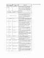
USART Communications Card Parts List
Label
Description
IC1 - IC4
IC12, IC14, IC20,
IC22
IC11, IC13, IC19,
IC21
8251, 28-pin, USART interface chip
1489, 14-pin, quad line receiver
4 (1)*
4 (2)*
Digital Group
Part #
073-015
078-007
1488, 14-pin, quad line driver
4 (2)*
078-008
j(
~
l(
IC26
IC18
IC7
IC25
IC10
IC17
IC15.IC16
IC5,IC6
IC8,IC9
IC23.IC24
74154, '14-pin, 1 of 16 decoder
7420, 14-pin, dual 4-input nand gate
74L04, 14-pin, hex inverter
7442, 16-pin, 1 of 10 decoder
7402, 14-pin, quad 2-input NOR gate
7432, 14-pin, quad 2-input OR gate
7401, 14-pin, quad 2-input nand gate
7493, 14-pin, binary counter
74193, 16-pin, synchronous binary counter
74125, 14-pin, tri-state quad buffer
1
2
2
2
2
075-053
075-011
075-049
075-016
075-002
075-013
075-001
075-023
075-041
075-031
{
Q1
01
2N5129 npn transistor
1N60 germanium diode
S1 - 84
S26
S8. S9, 825
S5 - 87. S10- S24
28-pin socket
24-pin socket
16-pin socket
14-pin socket
PC board
22-pin dual edge connector
36-pin dual edge connector
~
C5, C8. C9,
C11
C2
C1, C3. C4,
C6, C7. C10
1(
Y1
)t
)(
~
~
~
iii
X
-¢
~'
~
1;A
-rf>.
~
Ci'
.8t
)(
0
ON/p..
~
)!
R1. R2
R3
R4
Qty.
l
020-004
040-001
4 (1)*
1
3
18 (14)*
1
1
060-005
060-004
060-002
060-001
090-047
080-000
080-001
1 mfd, 15V tantalum capacitor
4
010-001
50 pfd, silver mica capacitor'
.01 mfd capacitor, ceramic
1
6
018-002
014-002
030-007
060-007
4 MHz crystal
Crystal socket
1K ohm '/4 watt carbon film resistor
10K ohm '/4 watt carbon film resistor
100 ohm v.. watt carbon film resistor
* If you have ordered a COMM-1, quantities in parentheses are supplied.
-22-
2
1
1
001-025
001-037
001-010
NOTE: FOR MORE RELIABLE OPERATION, USE 8251A
NEe mIcrocomputers, inC.
,uPD8251
PROGRAMMABLE COMMUNICATION INTERFACE
oESC R I PT ION
F EA TU R ES
The J,1PD8251 Universal Synchronous/Asynchronous Receiver/Transmitter (USART) is
designed for microcomputer systems data communications. The USART is used as a
pel iphel "I dnd is pi ogrammcd by the J,1PD8080 or other processor to communicate in
commonly used serial data transmission techniques including IBM Bi-Sync. The USART
receives serial data streams and converts them into parallel data characters for the
processor. While receiving serial data, the USART will also accept data characters from
the processor in parallel format, convert them to serial format and transmit. The USART
will Siqllill thn PI ocessor when it has completely received or transmitted a character and
requires service. Complete USART STATUS including data format errors and control
siqn,t\<, slIch as TxE and SYNDET is available to the processor at any time.
• Asynchronous or Synchronous Operation
•
•
•
•
•
•
•
•
•
Asy nchronous:
5-8 B it Characters
Clock Rate - 1, 16 or 64 x Baud Rate
Break Character Generation
Select 1, 1-1/2, or 2 Stop Bits
False Start Bit Dr.tec10r
Synchronous:
5-8 Bit Characters
I nternal or External Character Synchronization
Aut om<lt ic Sync Insertion
Single or Double Sync Characters
Ballu Rate - Synchl unous - DC to 561< B(Juu
- Asynchronous - DC to 9.6K Baud
Full Duplex, Double Buffered Transmitter and Receiver
Pal ity, Overrun and Framing Flags
Fully Compatible with 8080
All Inputs and Outputs are TTL Compatible
Single +5 Volt Supply
Separate Device, Receive and Transmit TTL Clocks
28 Pin Plastic DIP Package
N-Channel MOS Technology
PIN CONFIGURATION
02
01
03
DO
Vce
fhD
GND
RxC
f)1l
DTR
RTS
05
06
D/
J,1PD
8251
DSR
CLK
WR
TxD
cs
TxE
C/U
C;TS
RxROY
Five M iliticY D rive/Lexmgton, Massachusetts 02173
c/o
Contlol or Data" 10 he Written or Rr~rJ
RO
Read Data Command
CLK
Clock Pulse (TTL)
TxC
Trammltter Clock (TTL)
:s:su-~-~~·--=--==--=-~===---~-=
~T=x~O__+T~ra~-.~n~~m='t~-O-at-a--------------RxC
Receive' Clock (TTL)
RESET
1 xC
RD
PIN NAMES
~_Q_+_Oa_ta_B_us_(_8_bl_s)_ _ _ _ _ _ _ _ _ _ _
SYNDET
Vee
>5 Vol t Supply
GNO
Ground
TxRDY
Telephone 617/862-6410
Rev/1
Telex 92-3434
TWX -710-326-6520
The /JPD8251 Universal Synchronous/Asynchronous Receiver/Transmitter is designed
specifically tor 8080 microcomputer systems but works with most 8-bit processors.
Operation of the 8251, like other I/O devices in the 8080 family, is programmed by
system software for maximum flexibility.
FUNCTIONAL
OESCR IPTION
In the receive mode, a communication interface device must convert incoming serial
format uata into p(Jraliel data and nwke cen,lin formJt checks on the d(lta. And in'the
transmit mode, the device must format data into serial data. The device must also supply
or remove characters or bits that are unique to the communication format in use. By
perforrning conversion and formatting services automatically, the USART appears to the
processor as a simple or "transparent" Input or output of byte-oriented parallel data.
BLOCK DIAGRAM
II~flNSMII
BUFFER
TxD
IP ·SI
TxRDY
TRANSMIT
CONTI~OL
IT,H
TxE
--·-0
ilill ____ {)
nECFlvr
~'l!)I)I-M
H
F, _.-
IiUI I III
IS ·1'1
nJNIIHJI
('-Ic,'-0
/
Hf.Cf IVr.
CONTROL
IN rEHNfll
[)fI I fI IllJS
c/o
-
-
BASIC OPERATION
CS
RD
WR
0
1
0
1
0
0
Data Bus -+ 8251
1
0
1
0
Status
Data Bus -;- Control
0
8251
0
1
1
0
0
X
X
X
1
X
1
1
0
'-7
Data Bus
-+
Data Bus
Data Bus -. 3-State
'-----
T (~mp(\1 ,ltUrt~
Temperature
All Output Voltages
/\11 Inplil Volt;HWs.
Supply Voltages ...
- O°C to +70°C
-65°C to +125°C
0.5 to +7 Volts
- 0.5 to +7 Volts
'0.5 to +7 Volts
OPt'1 dtlll\)
Stnra~w
COMME NT: Stress above those listed under Absolute Maximum Ratings" may cause permanent
dilll1dfJ(? to the deVice. ThiS is lJ st'CSS Idtmg only and functional operation of the device at these or
any other conditions above those mdlcated ill the operatIOnal sections of this specification is not
IlllpllPd_ E XP()~lll n tn absolute mdXlrnum rnt InO conditions for extended periods may affect device
lel1abtllty.
II
2
ABSOLUTE MAXIMUM
RATINGS*
DC CHARACTE R ISTICS
Ta =
o°c to 70°C; VCC '" 5.0V
5%; GND '" OV
!
LIMITS
PARAMETER
SYMBOL
MIN
TYP
MAX
UNIT
Input Low Voltage
VIL
GND -.5
0.8
V
Input High Voltage
VIH
2.0
VCC
V
Output Low Voltage
VOL
Output High Voltage
VOH·
Data Bus Leakage
IDL
0.45
2.4
CAPACITANCE
TJ
I nput Load Current
IlL
Power Supply Current
ICC
25"C; VCC "GND
·
PARAMETER
V
IOL=1.7mA
V
IOH
-50
IJ.A
10
80
= -100 IJ.A
VOUT
VOUT
10
45
TEST CONDITIONS
J.LA
= 0.45V
= VCC
@5.5V
mA
OV
'"C
SYMBOL
MIN
LIMITS
TYP MAX
TEST CONDITIONS
UNIT
,1 MHz
Input C;lpilcltance
CIN
10
pF
fc
1/0 (;.Q),IClt;1I1C1)
CliO
20
pF
Unmeasured pins leturned
to GND
'-------
K
L
PACKAGE OUTLINE
I1 PD8251C
0° __ 15"
IHM
MILLIMETERS
INCHES
r--~__ -4___3_8_.0_M_A_X_._~_I_.4_9_6_M_A_X_.~
B
7.119
C-
2.54
0.09R
f------j----------- -+------i
._-------_..
0.10
_- _._----
0.5' 0.1
D
0.02
I
U.004
1.:1
. 33.02
F
1.5
0.059
G
2.54 MIN.
0.10 MIN.
H
0.5 MIN
0.02 MIN .
5.72 MAX.
0.225 MAX.
.- - - - f------------+---------t
I
5.22 MAX
0.205 MAX.
15.24
K
.-
. -- .. -.---
0.6
----- -_. -_._._-----
13.2
0.52
r--~---~---------r-----~
M
to 004
10.10
______ .~~:_9cQ:..:::.5___'__0_0_1_0_.0_QL
3
(D
BU!. PARAMf H RS
AC CHARACTERISTICS
vee - !,.OV .
(I' C '" /0 C
T..
nv
!l%. GND -
PARAMETER
LIMITS
SYMBOL
UNIT
MAX
TYP
MIN
TEST CONDITIONS
RfAD
~o
'IIA
-
~~~~II'
r-.::;:,,;;~~~~~:~~'-~~~~!-
_
'111\
,' ... ... "
,..... " .... ' ..... ,- ""_ ....... ... "'_ .......... _. -.-.::~--r--..-------_'.:,:H.:,:I1___+ - 4 - 1 ( - J - - l - - - - l - - - - + - - - + - - - - - - - - i
._
---~.
..-._________.___ :!..~_____+_----I--_---I--35-0--+_---+--C.!:.L-I-00~PF-___j
HI 1I1l,·,Il.", '1'1.1'111"
CL - 100 pr
~()()
'IJI
~.___._ _ _ _ _ _ _ _ _ _ _ _ _ _ _ _ _ _ __+--2-5--+---+----_+----+--C-L~o-I-5~pF--4
HI.,
Ijv'~1 y I itTif' Il,·, VYP'lll WH 11 E S
Q)
'CY
WAITE
Add"" . .
-::w=rl=Ii=1=--_____+-__'~II.:!W.!.___+-...:'}:..:O--+_----+_---_+---'--_+-------_I
',1,11,1,·,_"_"'_"_"
400
[),lIo! S~,
Up Time
'0'
WRITE
200
'IlW
40
'WLJ
OTHER TIMING
(,jurk Period Gil
f-----
1.I'lI k
--t--
-- - - - - - - - - - - - - - - - H"""'HI' .111 Tlmp
135
420
'CY
,'"l( " Pu!\tI WidTh
1'.IW
220
------I------~-----
0.71CY
so
'H,IF
~---------~===----l_~~-~----l_--_4-----l_--~~---
0'
I-~~~~~~~~~~.~~,~-=-~g Edq~
hC
~~''\!.l liPI Uo r ,ryw 10 S.Jmpl,nq Pul~e
'Oh __-+____+-_ _ _+-____ +
__-~
___-t-_ _C-'·L:...,·_10_0,.;,P_F_--l
J.I~
'SHl(
CL
100 pF
_~~~:~_'.._H_U_'{!_T~_fl)f_''_"_Sa_rr~~~~I_'e_ _ _ _ _ _~'H~R.:..,.~ _ _+_----l_---_+-----+_-IJ-s--t---C-'L=--.-10-0-p-F-_I
'T>.
1 X B,lIl(l H.I't~
HiX .. ndfi4XH,l'Hlri,ttt'
oc
~
K~
OC
520
KHl
---------- -----.------- --- - - ---+---=---+----+~--+~~-+_----~----1
lr,ln,lntll",
1)( RoIlJd
InplJI (Io( I..
Putsp \'\I,d,.,
11 P\"IJ
n,lil'
H, X ,1lld (;4 X !i.Hn! H,tll'
-.----_.. - ---- -----..- ..------------
1"}
'CV
1
'CY
-- _. -------+----_._._--)----" PD
1',
It;X .nd 1,·1" Holl/I! H .• ".
'CY
:1
'CY
or
KHz
KHz
- - - - - - -- ----------------- --------------HI·tt·rver InI.JU! ( lork
r ,.,qulmcy
lRx
1 X B.lud Rill'
IlIx , I,d fill '< H,Hld H .. H'
()C
-------------------------------+---------~~----+-------+------+----+--------~
r~PI t'IVl" Input ('II)( ~ Pulw Wtdlh
'HPW
17
1 X 1l.llld H,lt"
'CY
~-'6-x-.-n-tl-(j-4-X.~~I~~~~_ _ _ _ _ _ I__----t_____-'---+----+-.---+-.:::'C~Y'--_4-------_1
Ill" tJl1d'f If'llll! ('1,11 ~ P,lf'..., 11t'1"",
'llPI)
I',
ICV
'Cy
It.iX tInt! (4)< !IoIUI! H.J'~'
1---------- - - - - - - - - - - - + - - - - --+----4----f-.----t--.:.:..c.-_+----------I
r "f~I)Y 1I"'.IY ",lfn l't'IlIt'1 of 1).11" n,1
_ 'r_~ _ _ ~.~-----+----+_--:1f-.-; _-+_..:.'C:.;y_.-+___
C:..,l_5_0.:.,P_F_---4
Hlo,~iDY l),·I.ty '"'Hn Cpot"1 of Ddt,} ntl
'Hx
!----------------------------I--------11"I'IIl,I!
() ltd
"v'lth"
i' .. 1 1\; t',lln
{"'!lIrl of
H"
~-;:"~(I~~~:;--IJP
20
ICY
2!.J
'CY
If)
ICY
----.-+-----+------+-~-_+-------_1
Tlmf' J)Pll)lf>
I dl'llq I ,!q,' ,d H,l
'f~;
•
16
1-~E~1Pl-';;C),·j~~'!:~;;(:-;;I_;_;~-~I-O-,~;:;i·\-:~-------1f:E---------1G
ICY
CL
50pF
- -- - --------------..- - -..--f------=----+----I------+----+-~-+_-~'-------__{
,nlllllj)l'l,v 11_'1~11 '~.i\I~Hl f ,jllf'llj
r--~~IIl!lpllP
I~tl\t).. _______________
S,ot (Jp T,mp tC5'STI, ('TSI
________
\JIll,'"
~
'( f4
ICY
_
_ _ _ .___1;.,;:6'--_-'-_ _ .--.J__'__ _ _ _..L.--..:~_-'_ _ _ _ _ _---l
\.1'
1\(
(:)\
Th,<. recovery Ilmt· is lor Intll,tI'/dlll)n only. wtwn MODE, SYNC1, SYNC:', COMMAND ,)nd filS! DATA BYTES Me written InfO
lnnlflg'> me.l\un·d .II VOH
Ihl·ll';~\Hl
t.))
/,0, VOl
~;IIIJ,.I.qUI'f\' Wi"lllq III l)(lIh
0 H. ,Ind with IOdd lllCUtl of f-.lqlJlC 1
COl\1f\1I\ND ,Ind DA 1 A
,tli'
Iinly .. lIowl.1! wilt·n T .. HDY
1
Ttw TxC ,lOci ~h.C Ilcqucllnes hdve The following IlInlti1l1ons V\ll1h resperl 10 eLK
fpl
IX R,Hnj H,llf', 'T>. or In .. '
1/1301cyl
+20r-----r-----r-----r-----,
2V
V'l
C
Gl0H
>-
+10
<!
....J
W
0
I-
0
:J
D.U.T.
Cl.
I-
:J
0
24KU
-:-
-10
<I
--20
-100
-50
0
+50
+100
.:::l CAPACITANCE (pF)
Figure 1.
Typical!:::. Output
Delay Versus!:::' Capacitance (pF)
TEST LOAD CIRCUIT
4
", y~__._-.....,J-----.,,'--_-..J1r-------\_____
TIMING WAVEFORMS
( B
('S-
- - - - - "'1'---------------':'--------+-+--"_
I) I 1'1, _ _ _ _ _
WRI1E
------------------~\~-----------~twc---*
TxE,DTH,R1S
----------------------------
----------------------------
OSF~~~:------------------------------------------~X:f:===~I-~-Il------------------~/:========================~
READ AND WRITE TIMING
_ - - - - - - - I TPW ----- -- - -
_ _ --- ___ I TPD -----____ _
1 xC 11 x IlAUDI
1 - - - - - - - - - - 1 6 hC PER 10 D S - - - - - - - - - - . j
TxC 116x BAUD I
!xl)
r-
-
-- -
I01X
f~-
TRASNMITTER CLOCK AND DATA
Ihl)
iT;( II, IIAUDI
INTFHNAI
':IIMI'IIN(j
put SL
xU
R
j -----
=i=-)--'---ISRX-+-~IHHX-
~ ______
----IRPW ____
_________________________
--4:----
~-----_-IH-P-O--------------
~n~
1'------
__________________________
S1AH 1 HI T----~t::::===~l.::;. I~D~A~T~A~B~ll~===;Jc=
I'----------------~....,-;~
- =-,-= - "7H;X=-=-..:t".J~----
HxC 110x £IAUDI
INTERNAL
SAMPL
ING _ _ _ _ _ _ _ _ _
~
'-_ _ _ _ _ _ _ _ _ _ _ _--''-_ _ _ _ _ _ _ _ _ __
PULSL
RECEIVER CLOCK AND DATA
IhO
-r
STAf11 Bill
DATA BITS!
HxROY
-----------------------------------~
f1EAO ------------------------------------------~
G~:~~~~~~~~~~~tTx~~~I~~~~
WR'TE~
I~
WRITE 1st BYTE
WHITE 711<1 IlYH
WRITE 3rd BYTE
1.0 MA~ S r AR 1 B IT I"~D'!"'A"""!"'TA~B'"'!ll~S~~';r-----..,Fl'!p~A-=R~1T~Y~B-IT'TI-S-TO--P\:-"B-I-T'""'lsT AR T BIT
-I-
~------ht DATA BYTE
r--
7r1<i DATA flYTr
TxRDY AND RxRDY TIMING (ASYNC MODE)
I-
SYNC CHARACTER 101101001)
---------0---11
Ilxl)~_ _ _ _ _ _ _....~
F-C
=]AST 8ITIr---,,lIS
SYNDET
__
10UTPUT)-------------------------------------------------------
INTER!'IAL SYNC DETECT
SYNOET
IINPUTI
,-n--,. . .___. . .
l..._ _ _...
RxC - - - - ,..._ _ _- '
------=-411-_
12
tES
EXTERNAL SYNC DETECT
Note:
CD Write and Read pulses have no timing limitation with respect to elK.
5
RESET BY
SOFTWARE
COMMAND
PIN IDENTIFICATION
PIN
NO.
SYMBOL
1,2,
27,28
5-8
NAME
Data Bus Buffer
26
VCC
GND
4
FUNCTION
An 8-bit, 3·state bi-directional buffer used to
interface the 8251 to the processor data bus.
Data IS transmitted or received by the buffer in
response to input/output or Read/Write instructions from the processor. The Data Bus Buffer
also transfers Control words, Command words,
and Status.
Vec Supply Voltage
+5 volt supply
Ground
Ground
Read/Wlite COrltlol lODIC
This logic block accepts inputs from the processor Control Bus and generates control signals
for overall USART operation. The Mode
I nstructron and Command Instruction registers
that store the control formats for device functional definition are located in the Read/
Write Control logic.
21
RESET
Reset
A "one" on this input forces the USART into the
"Idle" mode where it will remain until reinitialized with a new set of control words. Minimum
RESET pulse width is tCY.
20
ClK
Clock Pulse
The ClK input provides for internal device timing and is usually connected to the Phase 2 (TTL)
output of the pPB8224 Clock Generator.
External Inputs and outputs are not referenced
to ClK, but the ClK frequency must be 30
times the Receiver or Transmitter clocks in the
synchronous mode and 4.5 times for the
asynchronous mode.
10
WR
Write D<Jw
A "lei 0" on this input instructs the pPD8251
to accept the data or control word which the
processor is Writing out to the USART via the
data bus.
13
RD
Read D,Ha
A "zero" on this input instructs the pPD8251
to place the data or status information onto the
Datn Bus for the processor to read.
C/O
Control/Data
The Control/Data input, in conjunction with the
WR and R D inputs. informs USART to accept or
provide either a data' character, control word or
status information via the Data Bus.
0= Data; 1 == Control.
I-----t.--==-----f-----------~-------------------__I
11
CS
Chip Select
Modem Control
Data Set Ready
22
r---------.24
A "zero" on this input enables the USART for
reading and writing to the processor.
The pPD8251 has a set of control inputs and
outputs which may be used to simplify the
Interface to a Modem.
The Data Set Ready input can be tested by the
processor via Status information. The DSR Input
is normally used to test Modem Data Set Ready
condition.
-==---- f---------.---...---_+_---.-------------------i
f- ..
DTR
Data Terminal Ready
The Data Terminal Ready output can be controlled via the Command word. The DTR output
is normally used to drive Modem Data Terminal
Ready or Rate Select lines.
~.--~====---+-------------+-------------------------------i
23
RTS
Request to Send
The Request to Send output can be controlled
via the Command word. The RTS output is
normally used to drive the Modem Request to
Send linc.
17
CTS
Clear to Send
A "zero" on the Clear to Send input enables the
USART to transmit serial data if the TxEN bit in
the Command Instruction register is enabled
(one).
6
TRANSMIT BUFFER/
CONVERTER
The TI ansrnit Buffer/Converter receives parallel data from the Data Bus Buffer via the
il)leillal data bus, converts parallel to serial data, inserts the necessary characters or
bits needed for the programmed communication format and outputs composite serial
uata 011 the TxD output.
PIN IDENTIFICATION
PIN
(CONT.)
NO.
FUNCTION
NAME
SYMBOL
The Transmit Control logic accepts and outputs
all external and internal signals necessilry for
serial data transmission.
Transmitter Read.." signals the processor that the
transmitter is ready to accept a data character.
TxRDY can be used as an interrupt or may be
tested through the Status information for Polled
operation. loading a character from the processor automatically resets TxRDY.
The Transmitter Empty output signals the
processor that the USART has no further characters to transmit. TxE is automatically reset
upon receiving a data character from the processor. In half-duplex, TxE can be used to signal
end of a transmission and request the processor
to "turn the line around." The TxEn bit in the
command instruction does not effect TxE.
Transmit Control logic
TxROY
Transmitter Ready
18
TxE
Transmitter Empty
In the Synchronous mode, il "one" on this Olltput indicates that a Sync character or chilracters are about to be automatically transmitted
as "fillers" because the next data character has
not been loaded.
---9
TxC
Transmitter Clock
The Transmitter Clock controls the serial character transmission rate. In the Asynchronous
mode, the TxC frequency is a multiple of the
actual Baud Rate. Two hits of the Mode Instruction select the multiple to be 1 x, 16x, or 64x
the Baud Rate. In the Synchronous mode, the
TxC frequency is automatically selected to
equal the actual ~alJd Rate.
Note that for both Synchronous and Asynchronous modes, serial data is shifted out of the
USART by the falling edge of TxC.
19
TxD
Transmitter Data
The Transmit Control logic outputs the
composite serial data stream on this pin.
_0
8251 INTERFACE TO 8080
STANDARD SYSTEM BUS
15
)
\
ADDRESS BUS
AO
~
CONTROL BUS
-I/O R
~.
I/O W
RESET
4>2
(TTL)
\
DATA BUS
A
8
0
--
C/O
-CS
V
07 - DO
(')
-RD
8251
7
'>
0
-WR
RESET
elK
Tile necl)ivcl Bufful Jccepl!> ~l!llill ddlu input ut Ilw HxD pin and converts the data
from serial to parallel format. B its or char acters required for the specific communicatioll technique ill use ,.lie checked and then an eight-bit "assembled" character is
readied for the processor. For communication techniques which require less than
eight bits, the pPD8251 sets the extra bits to "zero."
PIN IDENTIFICATION
PIN
NO.
SYMBOL
FUNCTION
NAME
Receiver Control Logic
111
This block manages all activities related to
incoming data.
fhRDY
The Receiver Ready output indlc(ltes that the
Receiver Buffer IS ready with an "assembled"
charilcWr for InrllJt to the processor. For Polled
operation, the processor can check RxRDY
using (l Status Rf!cld or RxRDY can be connected to the processor interrupt structure.
NOI<~ that r(~;J(linq thp. character to the processol lIutomatlcally resets HxHLJY.
RxC
1 tw R[~CI!IVer Clock is the rilte .. t which the
incoming choracter is received. In the Asynchronous mode, the R xC fr~~quency may be 1,16
or 64 times the actual Baud Rate but in the
Synchronous mode the RxC frequency must
equClI the Baud Rate. Two bits In the mode
instructIOn self~ct Asynchronou<; Clt 1 x, 16x or
64x 01 Synchronous operation at 1 x the Baud
Rate.
Unlike TxC, data IS sampled hy the }.!PD8251
on the Iising edqe of RXC. Q)
3
16
Note:
~-----------------~
RxD
Receiver Data
A composite serial data stream is received by
the Receiver Control LogiC on thiS pin.
SYNDET
Sync Detect
The SYNC Detect pin is only used in the
SYllclliOI10U" mode. The }.!PD8251 may be plOgrammed through the Mode InstructIOn to
opelate In either the Irltclnal or external Sync
mode and SYNDET then functions as an output
or Input respectively. In the internal Sync mode,
the SYNDET output will go to a "one" when
the /-lPD8251 has located the SYNC character
In the Receive mode. If double SYNC
character (bi-sync) operation has been programmed, SYNDET will go to "one" in the
middle of the last bit of the second SYNC
character. SYNDET IS automatically reset to
"zero" upon a Status Read or RESET. In the
external SYNC mode, a "zero" to "one" transition on the SYNDET input will cause the
}.!PD8251 to start assembling data character
on the next fallmg edge of RX'C. The length of
the SYNDET Input should be at least one RxC
perrod. but may be removed once the
}.!PD8251 is in SYNC.
CD
Examples:
RECEIVER BUFFER
Since the ~jPDB751 will flequently be handling both the reception and transmission
101 a Ylven IlI)k, the Hl!CeiVe and '1 tHlsrnit BaUd Rates will be same. Rxe ()nd lXC
then require the same frequency and may be tied together and connected to a single
clock source 01 i:3;Jud Rate Generator.
If the Baud Rate equals 110 (Async):
If the Baud Rate equals 300:
RxC or TxC equals 110Hz (1 x)
RxC or TxC equals 1.76 KHz (16x)
~ or TxC equals 7.04 KHz (64x)
RxC or TxC equals 300 Hz (1x) A or S
RxC or TxC equals 4800 Hz (16x) A only
or TxC equals 19.2 KHz (64x) A only
Axe
8
(CONT.)
OPERATIONAL
DESCRIPTION
A set of control words must be sent to the /lPD8251 to define the desired mode and
communications format. The control words will specify the BAUD RATE FACTOR
('lx, 1Gx, G4xl, CHARACTEH LENGTH (5 to 8), NUMBER OF STOP I1ITS
(1, 1-1/2,2), ASYNCHRONOUS or SYNCHRONOUS MODE, SYNDET (IN or OUT),
PARITY, etc.
After receiving the control words, the /lPD8251 is ready to communicate_ TxRDY is
t aised to signal the processor that the USART is ready to receive a character for trammission. When the processor writes a character to the USART, TxRDY is automatically reset.
Concurrently, the /lPD8251 may receive serial data; and after receiving an entire
character, the RxRDY output is raised to indicate a completed character is ready for
tile processor. The processor fetch will automatically reset RxRDY.
Note: The /lPD8251 may provide faulty RxRDY for the first read after power-on or
for the first read after receive is re-enabled by a command instruction (RxEI.
A dummy read is recommended to clear faulty RxRDY. But this IS not the
case for the first read after hardware or software reset after the device
operation has once been established.
The /1PD8251 cannot transmit until the TxEN (Transmitter Enable) bit has
been set by a Command Instruction and until the CTS (Clear to Send) input is a
"zcro". TxD is held in the "marking" state after Reset Clw{Jiting new Command
Words.
J-lPD8251 P R OG RAM MIN G
The USART must be loaded with a group of two to four control words provided b'/
the processor before data reception and transmission can begin. A Reset (internal or
external I must immediately proceed the control words which are used to program the
complete operational description of the communications interface. If an external
RESET is not available, three successive 00 Hex or two successive 80 Hex command
instructions (C/O = 1) followed by a software reset command instruction (40 Hexl
can be used to initialize the 8251.
There are two control word formats:
1. Mode Instruction
2. Command Instruction
MO 0 E I NST R UCTI 0 N
COMMAND INSTRUCTION
This control word specifies the general characteristics of the interface regarding the
SYNCHRONOUS or ASYNCHRONOUS MODE, BAUD RATE FACTOR, CHARACTER
LENGTH, PARITY, and NUMBER OF STOP BITS. Once the Mode Instruction
has been received, SYNC characters or Command Instructions may be inserted depending on the Mode Instruction content.
This control word will be interpreted as a SYNC character definition if immediately
preceded by a Mode Instruction which specified a Synchronous format. After the
SYNC character(s) are specified or after an Asynchronous Mode Instruction, all subsequent control words will be interpreted as an update to the Command Instruction.
Command Instruction updates may occur at any time during the data block. To
modify the Mode Instruction, a bit may be set in the Command Instruction which
causes an internal Reset which allows a new Mode Instruction to be accepted.
9
C/O'" 1
MODE INSTRUCTION
C/I) - 1
SYNC CHARACTER 1
=1
SYNC CHARACTER 2
C/O
C/O =- 1
ONLY
CD
,'"
DATA
C/O = 1
COMMAND INSTRUCTION
CIO
0
I,.
/is
-= 1
C
CD
SYNC MODE
}
COMMAND INSTRUCTION
c/o a ,,
NOTE
TYPICAL DATA BLOCK
DATA
COMMAND INSTRUCTION
The second SYNC chilrLlcter IS skipped if MODE instruction
has programmed the 8251 to single character Internal SYNC
Mode. Both SYNC churacters LIre skipped If MODE instruction
has programmed the 8251 to ASYNC mode.
The ,uPD8251 can operate in either Asynchronous or Synchronous communication
modes. Understanding how the Mode Instruction controls the functional operation
of 1111' lJSI\RT is p,lsi(!SI whl!n tlw dl!vic:c is consid(!r(!d to he two separatp. components,
one asynchronous and the other synchronous, which ~hare the same support circuits
and package. Although the format definition can be changed at will or "on the fly", the
two modes will be explained separately for clarity.
MODE INSTRUCTION
DEFINITION
When a daw character -is WI I tten into the ,uPD8251, the USART automatically adds
a START bit (low level or "space") and the number of STOP bits (high level or
"mal k ") specified by the Mode Instruction. If Parity has been enabled, an odd or
evp.n Parity bit is inserted just before the STOP bits(s), as specified by the Mode
Instruction. Then, dependlllg on CTS and TxEN, the character may be transmitted
lIS d SCI idl data stleam ilt the TxD output. Data is shifted out hy the falling edge of
TxC at -[xC, TxC/16 or TxC/64, as defined by the Mode Instruction.
ASYNCHRONOUS
TRANSMISSION
If 110 datIl Chill acters have hl'I!!) loaded into the I)PD8251, or if all available characters
have been transmitted, the TxD output remains "high" (marking) in preparation
for SPIHilllg the ST ART hit of the next character provided by the processor. TxD may be
fmcpd to send (l BREAK (continuously low) by settin!1 the correct bit in the
Command I nstructioll.
ASYNCHRONOUS
The RxD input line is normally held "high" (marking) ,by the transmitting device.
A failing edge at RxD signals the possible beginning of a START bit and a new
RECEIVE
ChcHilcter. The START bit is checked by testing for a "low" at its nominal center
as specified by the BAUD RATE. If a "low" is detected again, it is considered valid,
and the bit assembl ing countel starts counting. The bit counter locates the approx imate center of the data, parity (if specified), and STOP bits. The parity error flag (PE)
is set, if a parity error occurs. Input bits are sampled at the RxD pin with the rising
edge of RxC. I f a high is not detected for the STOP bit, which normally signals the end
of an input character, a framing error (~E) will be set. After a valid STOP bit, the input
character is loaded into the parallel Data Bus Buffer of the J,1PD8251 and the RxR DY
signal is raised to indicate to the processor that a character is ready to be fetched. If the
processor has failed to fetch the previous character, the new character replaces the old
and the overrun flag (OE) is set. All the error flags can be reset by setting a bit in the
Command Instruction. Error flag conditions will not stop subsequent USART operation.
10
MODE
INSTRUCTION FORMAT
ASYNCHRONOUS MODE
S7
S1
EP
PEN
L2
82
L1
B1
BAUD RATE FACTOR
----
0
1
0
1
0
0
1
1
SYNC
MODE
(1 X)
(16X)
(64X)
CHARACTER LENGTH
0
1
0
0
0
1
1
5
6
7
8
BITS
BITS
BITS
BITS
PARITY ENABLE
FN/\RLE
0
1
1
DIS/\RLE
EVEN PARITY GENERATION/CHE CK
1 'EVEN
0 ODD
NUMBER OF STOP BITS
0
1
0
1
0
0
1
1
1
1 Yi
BITS
BITS
INVALID
TRANSMIT/RECEIVE
FORMAT
ASYNCH RONOUS MODE
rxD
BIT
2
ST~
MAHKING
BITS
L
TRANSMITTER OUTPUT
'---_ST_BI\_I~_T_-'--
FhD
_ _D_A_T_i:B
r _IT_S_..L-_ _ _-"
STOt;!
BITS
RECEIVER INPUT
CPU BYTE (5-8 BITS/CHAR)
DATA
C~~RACHR
I\SSEMI1I EO SERIAL DI\TI\ OUTPUT (TxD)
START
BIT
DATA CHARACTER
L -_ _ _ _~_ _ _ _ _ _ _ _~(~--_ _-----L------~-~
TRANSMISSION FORMAT
SERIAL DATA INPUT (RxD)
CPU BYTE (5-8 BITS/CHAR)
G)
DATAc+8
NOTEQ): IF CHARACTER LENGTH IS DEFINED AS 5, 6, OR 7
BITS; THE UNUSED BITS ARE SET TO "ZERO,"
RECEIVE FORMAT
11
L
SYNCHRONOUS
TRANSMISSION
As in Asynchronous transmission, the TxD output remains "high" (marking)
until the pPD8251 receives the first character from the processor which is usually
a SYNC character. After a Command Instruction has set TxEN and after Clear
to Send (CTS) goes low, the first character is serially transmitted. Data is
shifted out on the falling edge of TxC and the same rate as TxC.
Once transmission has started, Synchronous Mode format requires that the serial
data stream at TxD continue Jt the TxC rate or SYNC will be lost. If a data character
is not provided by the processor before the j.1PD8251 Transmitter Buffer becomes
empty, the SYNC character(s) loaded directly following the Mode Instruction will
be (Jutornatica"y inscl ted in the TxO data stream. The SYNC character(s) nre inserted
to fill the I ine and maintain synchron ization until new data characters are available
for transmission. If the pPD8251 becomes empty, and must send the SYNC character(s),
the TxEMPTY output is raised to signal the processor that the Transmitter Buffer
is empty and SYNC characters are being transmitted. TxEMPTY is automatically
reset by the I1CX t character from the processor.
TxEMPTY go high at the middle of the last data bit when the Transmit Register is
EMPTY. TxEMPTY goes low again as sync characters are transmitted. See figure below.
FOR SINGLE SYNC CHARACTER OPERATION
TxD
=x
DATA
X
DATA
X
SYNC
X
SYNC
=x
DATA
n
DATA WRITE
n
DATA
x=
n
rp
fTl
TxEMPTY
X
CENTER OF LAST BIT
FOR DOUBLE SYNC CHARACTER OPERATION (BISYNC)
TxD
=-x
DATA
X
SYNCl
X
SYNC?
X
X
DATA
rp
TxEMPTY
CENTER OF LAST BIT
lxD
=x
DATA
X
SYNCl
X
SYNC2
n
DATA WRITE
TxEMPTY
>C
n
n
n
DATA WRITE
DATA
'+l
X
DATA
n
X
DATA
x=
n
ff1
CENTE:R OF LAST BIT
In Synchronous Hecerve, chardctcr ~ynchronililtioll can be either external or internal.
If the internal SYNC mode has been selected, and the Enter HUNT (EH) bit
has been set by a Command Instruction, the receiver goes into the HUNT mode.
I ncoming data on the RxD input is sampled on the rising edge of RxC, and the
Receiver Buffer is compared with the first SYNC character after each bit has been
loaded until a match is found. If two SYNC characters have been programmed, the
next received character is also compared. When the SYNC character(s) programmed
have been detected, the j.1PD8251 leaves the HUNT mode and is in character synchronization. At this time, the SYNDET (output) is set high. SYNDET is automatically
reset by a STATUS READ.
If ex ternal SYNC has been specified in the Mode Instruction, a "one" appl ied
to the SYNDET (input) for at lenst one RxC cycle will synchronize the USART.
Parity and Overrun Errors are treated the same in the Synchronous as in the
Asynchronous Mode. Framing errors do not apply in the Synchronous format.
The processor may command the receiver to enter the HUNT mode with a Command
Instruction which sets Enter HUNT (EH) if synchronization is lost.
12
SYNCHRONOUS
RECEIVE
MODE INSTRUCTION
FORMA.T
SYNCHRONOUS MODE
SCS
ESD
EP
PEN
L2
L1
0
0
CHARACTER LENGTH
o
1
o
o
1
1
5
6
BITS
7
BITS
8
BITS
BITS
L-_ _ _ _ _ _ _ _........
o
PARITY ENABLE
(1 ,= ENAB LE)
(() '" DISABLE)
L-_ _ _ _ _ _ _ _ _ ___.....
L -_ _ _ _ _ _ _ _ _ _ _ _~
EVEN PArHTY GENE nATION/CHECK
1 ~ EVEN
0=000
EXTERNAL SYNC DETECT
1 = SYNDET IS AN INPUT
0= SYNDET IS AN OUTPUT
SINGL.E CHARACTER SYNC
1 = SINGLE SYNC CHARACTER
0= DOUBLE SYNC CHARACTER
TRANSMIT/RECEIVE
FORMAT
SYNCHRONOUS MODE
CPU BYTES (5-8 BITS/CHAR)
DATA
C~~RACTERS
ASSEMHLED SERIAL DATA OUTPUT OxD)
SYNC
CHAR 1
SYNC
CHAR 2
DATACH~R~;_C_T_E_R_S
_____
~
TRANSMIT FORMAT
SERIAL DA"r A INPUT (RxD)
SYNC
CHAR 1
SYNC
CHAR 2
DATACHA~~A_C_T_ER_S
CPU BYTES (5-8 BITS/CHAR)
DATAc:3
RECEIVE FORMAT
13
______
~
After the functional definition of the I1PD8251 has been specified by the Mode
Instruction and the SYNC character(s) have been entered, if in SYNC mode, the
USART is ready to receive Command Instructions and begin communication. A
Command Instruction is used to control the specific operation of the format selected
by the Mode Instruction. Enable Transmit, Enable Receive, Error Reset and Modem
Controls are controlled by the Command Instruction.
COMMAND INSTRUCTION
FORMAT
After the Mode Instruction and the SYNC character(sl, as needed, are loaded, all
subsequent "control writes" (c/5 "" 1) will load or overwrite the Command Instruction
IP9islt~l. A R(~s(~t operation (intt~rn;iI via CMD IR or external via the RESET input)
will cause the I1 P D8251 to interpret the next "control write", which must immediately
follow the ICSt~t, dS d Mode Instluctlon.
I t IS f Iequclltly I1eCeSSdl y fOI the pi OCl!~SOI to cX(lrninc the "status" of an active
interfllce device to determine if errors have occurred or to notice other conditions
which require a response from the processor. The I1PD8251 has features which
allow the processor to "read" the device status at any time. A data fetch is issued
by the processor while holding the c/5 input "high" to obtain device Status Information. Many of the bits in the SWlus register Clle copies of external pins. This dual
status arrangement allows the pPD8251 to be used in both Polled and interrupt
driven environments. Status update can have a maximum delay of a 16 clock period.
When a parity error is detected, the PE flag is set, and is cleared by setting the
E R bit in a subsequent Command Instruction. PE being set does not inhibit USART
()Pt~1
STATUS READ FORMAT
PARITY ERROR
,It 1011.
_ It the processor fails to read a data character before the one following is available,
the OE flag is set, and is cleared by setting the ER bit in a subsequent Command
Instruction. Although OE being set does not inhibit USART operation, the
pi eviously Iecelved chal actel is overwritten and lost.
If a valid STOP bit is not detected at the end of a character, the FE flag is set, and
is cleared by setting the ER bit in a subsequent Command Instruction. FE being set
does not inhibit USART operation.
Note:
CD
ASYNC mode only.
14
OVERRUN ERROR
FRAMING ERROR
CD
COMMAND INSTRUCTION
FORMAT
iJ,
I
I II
I
III
III I
~,
I
I HI·.ulll<l H_l
11)111 I'-IN
[
TRANSMIT ENABl E
1 en~hle
llosable
0
DATA TERMINAL
fl['AI)Y
"hlqh" will force
output to lurO
5T'R
HECEIVE ENABLE
1 ~ enable
disoble
o '.
SEND BREAK
CHARACTER
1 forces TxO "low"
o = normnl operallon
ERROR RESET
1 rf!<'PI 0111 f!1 fOf
PE, OE, FE
tid" ...
REOUE'ST TO SEND
"hll)h" will fOlce HTS
output to zero
INTERNAl RESET
"high" return~ 32!J1 to
Modo In'itltJc1lon F-olrn.11
EN'r ER HUNT MODE
1 enablp sell, ch for Sync
Ch,H,J('lllI'!
u,
STATUS READ FORMAT
[
DSH
]SYNOU
1
1.
1
FE
111
OE
PE
I
'r xE
".ROY
I I
T.ROY
1 1
L
.
SAME DEFINITIONS AS 110 PINS
PARITY FllnOR
The PE 11,1(1 IS set when .J p,IIIIy
. en or IS detected. I t IS "'~et Ily
til" fl1 Ilil of tllH Cumrn;lIlIl
Instluctlon PE does not lI)hll"t
oper.llltll' of the 8?S1
---
OVERRUN ERROR
The OE flag IS set when the CPU
do!'s not rearl ;, char<Jcter hefore
the next one hecomps available.
It I~ roS"I hy II)!' [R hll of Ihe
C'OIl1Il1<11l" IIlSIrllctIlJl!. OL doe~
not 'nhlhll operntlon of the 8251,
however, the
character
IS
'HCVIOlJllly {)vprrUIl
lost
FRAMING FRIlOR (Async only)
The FE: ""9 IS set when ., v"lld
Stop bit IS not detecled at the
end of ('"ver V char actcr. I t IS re<;et
by the ER bit of the Command
Insl rue I ,on FE does not Inh,blt
Ihe OP"'"I,on of the 82(;1
NOle.
CD
TxRDY status bit ,s not totally equivalent to the TxADY output Pill, the relationship
follows'
1 ,ROY status b,t • DR Bulter Empty
TxRDY (pin 15) = DB Buffer Empty - CTS. TxEn
"ilS
15
APPLICATION OF THE J.LPD8251
CRT
TERMINAL
ASYNCHRONOUS SERIAL INTERFACE TO CRT TERMINAL,
DC to 9600 BAUD
1'1l0Nl
I IN~
Irllill
f
I\l'~
TELEPHONE
LINE
ASYNCHRONOUS INTERFACE TO TELEPHONE LINES
~,YNCIIH()NOlJS
II:HMINI\L
OR PEf1IPHERAL
I----<~-I
OE V Ie E
SYNDl TI-----~
SYNCHRONOUS INTERFACE TO TERMINAL OR PERIPHERAL DEVICE
SYNC
I'IH1Nf
IINI
INII ((
f ACI
~l()IJr ~1
11111'1l{)NI
LINE,
SYNCHRONOUS INTERFACE TO TELEPHONE LINES
The Information presented in this document is believed to be accurate and reliable. The information is subject to change without notice.
PRINTED IN U.S.A.
16
SP8251-5· 77-5K-GN
D269
0269:
0279:
0289:
3299:
02A9:
8289:
02C9:
8209:
02E9=
02F9:
0309:
~
0319:
0329:
0339:
0349:
47F83F0F
B1000000
00000000
00000000
A7FJ50J8
00000000
00000000
00000000
00000008
00000000
A8F25038
00000000
00080008
00000000
00000000
05800000
000096F7
00000000
00000000
00000000
00000000
00000000
00808000
00080000
00000000
00070000
00000000
00080000
00000000
00000000
00000000
00000000
00000000
00000030
00003833
00000000
00000000
00000000
00000000
00000000
00003800
00000000
00000000
00000000
00000000
-L I F2A8 116T
F2A8
F2AB
F2AE
F281
F.'?B4
E2B7
~9
'J"2BB
F2BE
JP
JP
0F35l
0F37B
0F3A2
.le
CB4F
IN
BIT
C5
PliSH Be
CAD8F2
JP
C,A
A,(lO)
E67F
CE:59
AND
BIT
7F
3. C
Z .. 0F2Dl
F2C6
2809
.JR
F2C8
CD74F3
F2CB
3E37
CALL 0F374
A.,37
LD
F2CD
D311
3E3F
OliT
F2CF
A.• 3F
Cl
LO
F2Dl
F2D2
POP
BC
CF66
SC
JR
66
F2DD
F2El
F2E5
F2E7
FOCE: lC46
BIT
200E
...1 F.:
A.,(11)
0 .• A
Z .. 0F33C
0 .. (I't+ lC)
HZ.,0F2F5
FDCB1C4E BIT
1.. (I'1'+lC)
F2E8
F2ED
2(100
JR
NZJOF2FA
BIT
2,(IY+1C)
...IF.:
HZ .. 0F31E
F2F8
F2FA
F2FD
F2FF
F301
F303
285B
1843
F07E1E
CE:7F
2800
E67F
SET
7)A
IN
LD
BIT
JR
0F339
A.. (lt)
IN
RLCA
.,JR
0F33D
A., ( I 't + lE)
LO
BIT
...IF:.
Z.,0F3(1E
AHO
7F
(IY+1E) .. A
Lei
F306
F0771E
FE13
CP
F3ec
F30E
2800
\ootR
F311
F312
F314
F3l6
-~19
-·''-..-318
F31C
B7
CIF~
11
Z;0F318
A.. (I,(+10)
A
2825
1826
FD7710
.JR
JR
0F33C
18F3
\ooIR
AF
~I,OR
FD7E1D
18F8
Lo
LD
\ootR
(I'r'+lCI) . A
0F30E
A
0F3l6
A.• (1"(+lE)
F321
F323
CB7F
2800
F325
..JR
E67F
F327
F0771E
FEet;
Z,d3F332
7F
(1'1'+lE) . A
F32A
ANO
LD
F32C
2004
CP
..JR
6
NZ.d3F332
FD7E 10
LCI
A.. (I,(+10)
F32E
F332
FD7E1E
FD361D00 LD
F335
FE80
F337
3003
F33A
37
1801
E:7
F339
F33C
F330
F340
F342
FD7E1E
CB7F
C9
CP
.,JR
0F33D
LD
BIT
A .• (I't+ lE)
'7 A
J
RET
E350
C9
CALL
...IR
LO
AHO
LO
F351
COB7F2
CALL
RET
1':"354
30FB
.JR
\ ~56
'- tt357
F359
79
031(1
LD
OUT
cs
RET
INC
Foes le56 BIT
F0341D
NC.d3F33C
A
COB7F2
F35E
80
JR
28FB
FD7E1E
EIS7F
FD771E
F350
(1'1'+10) .. 0
OR
F346
F348
F34D
7 .. A
SCF
F343
F34B
~.
13
LD
BIT
F31E
_.
(I~(+lE:) .d~
JR
F308 .. 2S@C- - . -.~-\;,tR---F30A FEll
CP
~.
C.,OF2B7
38El
CBFF
F0771E
D811
C:B47
FOCBte56
F2Fl ·2028
F2F3
1844
r-2F5 DB11
:2F7 07
...
Z,0F20B
lD
IN
F20F
--
,I/#Ir
l~A
0810
F2DB
~
IMr
A,(ll)
OF2B7
Z .• 0F343
A.,(I,(+lE)
7F
(IY+1E) .. A
0F2B7
NC .. 0F351
A. e
( 1(1 ) ; A
2.
(I~r'+lC)
Z
(1'1'+10)
••••••••••••••••
J
••••••••••••••••
' ............... .
P8 ...... 88 .... '
' ................
' ............... .
' ............... .
J
•
•
J
J
••••••••••••••••
J
••••••••••••••••
••
P8 ..... . 8.8 ...
J
J
J
••••••••••••••••
'
00000000 ) . . . . . . . . . . . . . . . .
00000000 ' ............... .
rA-TlltJ
IN
lA/IT
'G.? ............ '
J
0000~000 ' ............... .
$
0F343
4F
F2D4
~.,
0F287
F2C0
F2C2
F2D6
F208
~
oBl1
...lP
,JP
F2BF
F2C4
~ ..
C3B7F2
C343F3
CJ51F3
C378F3
C3 A ?E -.;;
0000B907
08030000
00030000
00000000
B800EF03
00000000
00000080
00000000
00000000
00000000
3800FF00
08000001
-B1 F2A8
t _I
0" 116T
J0(F C3B7'F2
at~03)
8006,1
O€109"
C343F3
C351.F3
C37BF3
!::J9?E"i'
000F" OB11
0(11) CB4F
010313" CADBF2
e~H3C"
0016"
0017"
0018"
€lOlA)
001C"
a'OLE)
(1'020)
0€123"
0~125"
\::t(27)
0029)
002A"
002C"
4F
0810
E67F
C859
2809
C074F3
3E3?
0311
3E3F
(:1
CF66
38E1
C8FF
F0771E
D811
CB47
.tR
IN
BIT
...IP
PUSH
0F J
98"
0A9"
003"
BEQ"
A.I (11)
1.. A
Z ~ 33..~_
Be
LD
C .• A
AND
BIT
7F
3 .. C
.JR
Z.,29·'
IN
11)f7f.tj
-
rt:~-J{"q-
-;
t
I
A .. (10)
CALL €ICC"
A .• 37
LD
'~11),.A
OUT
A,.3F
LO
POP BC
66
BC
.,JR
C .• 0F··
I
SET 7JA
(IY+1E)d~
LO
~
A.• (ll)
IN
0033"
0(135-'
BIT €I .• A
Z .. 94"
__ - - - ---,
0037,1 2858
.JR
r)t"~y
I.
6039" FOCB1C46 BIT \J;(1Y+1C)
\
"030) Z0eE
NZ .. 4D·'
...IR
I
1.. (IY+1C)
03F" FOCE: 1C4E BIT
NZ
..
52··
JR
'-0043" 2000
(1045-' FoeB 1.C56 BIT 2.· (I'r'+lC)
0049) 2028
....lR
HZ .. 76"
JR
91" - . - 0048" 1844
.
002E J
0030"
-
C5
,..IP
,JP
,JP
.JP
...-.~"''''
I
'-
-Bl F2AS
I e·' 116T
'- 'l3~00~ C3B7F2
03,1
. I.;;
0(106-'
0009"
'-
C3S lF3
C378F3
€H!10C" C:J!:1?E'"l
000F" 0811
CB4F
0011~
(1013,1
0016.1
'""
CAOBF2
C5
0017" 4F
....... EHa 1E.I
\,.....
C074F3
3E37
0311
3E3F
C1
CF66
38El
CBFF
F0771E
OB11
C847
002?"
0029,1
002A J
....... 002C"
0£12E)
0030"
' - 0033,0
0035"
0(3)
BEe"
IN
$TJ4~1
A .. (11)
BIT
,..IP
1 . (1
Z.,·3~~
PlISH Be
C .• A
LCt
IN
AND
8IT
-It~ K"q- -:
I
\
A .. (10)
7F
3. C
2 .. 29"
CALL acc"
A .• 37
LO
(ll).d~
OliT
A .• 3F
LO
POP BC
..JR
2809
012120,1
0023"
0025"
98"
eA9"
lR
........ 0018~
OB10
B01A" E67F
SOlC" C859
OFJ
...IP
...IP
..Jp
..JP
C343F3
SC
66
SET
7. A
.,JR
C .• 0F··
LO
IN
BIT
(IY+IE) .. A
A.• (ll)
0 .. (1
~
2 .. 94-'
__ --- -_ . . . . .,
.JR
137
<1
Y+
1
C)
T'')c J{ ~ ~ I.
BIT
0039" FDCBIC46
HZ .. 40"
..JR
13.:030" 200E
0037,1
'-..,
2858
63F-'
,
FDCBIC4E BIT
~043,o 200D
JR
"- 0045-'
FDCB1C56 BIT
0049)
2028
004B~ 1844
OB11
' - £104D"
004F" 07
0053" 1843
0852" FD7EIE
'0055" CB7F
0057,1 2800
0059,1 E67F
---. 005B" F0771E
805E J FE13
0060) 280(:
'- 0062,1 FEll
8064" 2800
0066) F07E10
"-- 8069" B7
006A" 2825
886(:) 1826
J
,-. 006E
F0771D
18F3
0073,1 AF
0074.1 18F8
"- 0076" FD7E1E
0079" CB7F
ft07S,I 280D
'-~701 E67F
07F" F0771E
8£182) FE06
0884.1 2804
'0086.1 FD361000
€leBA" F07El0
0080" FES0
'-- B08F" 3803
807'1
J
1Co.ItQ 10
,-
'01
LIJ
A., ( I 'i + 1E )'
7 .. A
2 .. 66"
7F
(I'r'+lE).,A
13
2>6EJ
11
2 .. 73"
A.,(I'r'+10)
OR
A
BIT
.JR
AND
LD
CP
..JR
CP
JR
..JR
Z .. 91"
JR
94"
LD
(IY+1D) .• A
66,1
XOR
A
6E)
A .• ( 1 ',(,+.lE)
JR
JR
LD
BIT
.JR
AND
LO
CP
JR
LO
LD
CP
JR
"
-\"-....- 0 A 3 .'
€t0ASJ
0~a~"
00A9"
BeAC"
~9
CDB7F2
28FB
F07E 1E
E67F
FD771E
~~
CDB7F2
30FB
80AE J 7~f
00AFJ 0310
OOB1) FOCE:1C56
00B5" (:8
80B6 J F03410
0089" F07E 1(1
00BC" FE7F
0ecBE" CIS
80BF" COB7F2
0ecC2" 30FB
88(:4" 3E03
00C6"
00CS-'
30CS"
7. A
Z .. 8A"
7F
(I'r'+lE) .. A
6
HZ.,8A"
(I'r'+ 10) .. (1
A.- (I 'r'+10)
80
UC . 94
\
J
\
---1..-.. -~-.-~ -
wC·r
OR
Qtt9EJ
'--;13A0"
'-
95"
LO
.JR
~7tB2a
'-...
JR
8094"
8095)
809B"
.......
IN
2 .. (1'(+1(:)
NZ .. 76,1
91 J
A .. (11)
RLCA
0(92) 1801
B7
FD7E 1E
809S" CB7F
.......
....IR
....IR
I
1..': 1'(+1(:)
NZ .. 52 J
LO
BIT
9C'"
fm'+lE>
7 .. R
R~I
CALL OF"
..JR
Z. 9B"
A .. (I't+1E)
LD
AND 7F
(IY+1E) .• A
LO
iEI
CALL 0F"
JR
LD
OUT
BIT
B-
(
IAJ
,wr
(}tq',,,,,-
Ne .. 0A9"
A .. C
(10) .• A
2 .. (I'(+lC)
RET
Z
INC
Lei
(I',{,+10)
A., ( I ~r + 10:>
7F
CP
RET
f
C
CALL 0FJ
NC.,0BF··
JR
A J '7
LD
.....
OUT (. 10) .' A
INC
RE
(IYtlC!)
BIT
0.d~
A .• (11)
80CEJ (:847
0000" 28FA
..
'-..
,
300"'''
3) 3EBE
0005" 0311
0£107" 3E40
C,809 .- 0311
apB"
'gOOF"
'-..,
00El,1
ee:1ES"
eOE?'OJ
...tR
Z.t €tCC"
LO
A .. SE
(11) .• A
A .• 40
(11)d:}
7., (I'r'+8)
-T
OUT
LO
OUT
FOCB087E BIT
280(:
...tR
FDCB0876 BIT
3E7A
LD
2006
.JR
-,r-rJ..
Z. €tEO"
6 .. (I ~i'+8)
A.- 7A
NZ .. 0EF-'
INlr
-
-------~--
-.
0092" 1801
'--- 0094) B7
0095) F07E1E
809S) CB7F
~,-
£1£1ge"
~9
809B" CD87F2
a09E" 28FB
--;'0A0" F07E1E
-''''----'~3A3J E67F
80AS" F0771E
-'--
~H3a~"
~~
00A9" CDB7F2
"-.--
LO
BIT
RsI
90BE" 08
0eBF" COB7F2
(10C2" 30FB
00C4" 3£03
00(:6"
e0CS"
(10CB"
,..IR
lO
AND
lD
0eo-:' .
£I 3"
0005"
3007"
3ESE
0311
3E40
t~809 .'
0311
, aOB" FOCB087E
'-e00F" 280(:
'-00E1" FOCB0876
9€1E5" 3E7A
00E7" 2006
'-9'0E9" 3E5A
0(1ES·t 1802
00EO" 3E4E
(10EF" 0311
00Ft" 3E37
00F3" 0311
00F5"
FCt361Ct00
'-..
00F9" C9
~HjFA·' 3E40
€l0FC" 031 i
€H3FE" C9
'-.--
.~~--
f
(I 'tHO
tJ
I
(
7 .• A
/AJ
~tAJr
2 .. 98"
A .. (11.(+lE)
7F
(I'T'+lE) .. A
BEl
CALL 0F"
NC .. 0A:)"
A .• C
(10)., A
2 .. (I,(+1C)
Ofl£7"""""
..,.:..
(1'-('+10)
A .. (I'r'+10)
7F
C
CP
RET
CALL OF
H(:.,0BFJ
JR
A.,3
LO
OliT (10:» A
J
INC
RET
'---
S0CE" CB47
0000" 28FA
gO;'
CALL 0F"
90Ae" 30FB
.JR
00AE" 7::1
LD
0(1t~F·1
0310
OllT
0081.1 FOCE:1C56 BIT
00B5,1 CS
RET
0086,1 F03410
INC
0089" F07E 10
LO
e0se" FE7F
"--
.,JR
OR
(1 Y+ 10)
A .• (11)
BIT
0 ...~
..JR
z .. 0ce"
R-T
LD
OUT
LD
OliT
BIT
...IR
BIT
LD
...If<
LD
...IR
'LO
OUT
LO
OUT
LO
A.,8E
(11) .• A
A.,4e:1
(11) .. A
7., (I'1'+8)
2.s\3E[tJ
6 .• (I~i'+8)
A .• 7A
HZ.,0EF"
A .• 5A
0EF"
A .. 4E
(11J .. A
A .. 37
(11) .. A
(1'1'+10) .. 0'
RET
LD
OUT
RET
A.,40
(ll) .. A
I'*',r
'41 111
,r