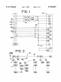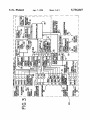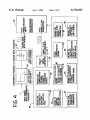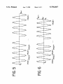
1
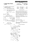
US005736847A
Q
Umted States Patent [19]
[11] Patent Number:
Van Doom et al.
[45]
[54}
[75]
Date of Patent:
4,979,122 12/1990 Davis et al. 5,017,360 5/1991 6911119! et al- -
LINES
5,059,896
10/1991 Germer et a1. .
5,061,890
10/1991 Langini ................................. .. 324/107
5 981313
1/1992 Yamada et a1‘ '
5,151,866
9/1992 Glaser 6t =11. ......................... .. 364/487
H. Lightbody; Chuen Shall Simon Ki‘
51171132311. .......................... .. 324/142
bah of “mm 4'1 °f Canada
_
'
'
5,155,836
Asslglleei CD Power Measurement Llmltei
Victoria. Canada
.
[21]
Apr. 7, 1998
POWER METER FOR DETERMINING
PARAMETERS OF MULIPHASE POWER
Inventors: Peter M. Van Doom, Sidney; Simon
[73]
5,736,847
Appl' No" 367534
[22] Filed;
Dec 30, 1994
[51]
[52]
Int. Cl.‘ ................................................. .. G01R 21/133
us. 01. ........................................... .. 324/142; 364/483
[58]
Field of Search .............................. .. 324/103 R. 107,
12/1984 Fletcher et a1. .
2/1978 Johnston et a1. .
5/1979 G|j$s _
4,240,149
12/1980 Fletcher et a1. .
4,345,311
:ggiggi
4’455’612
4:459:546
8/1982 Fielden
6/1993 Wallis .... ..
5,233,538
8/1993
5,243,536
9/1993 Bradford ............................... .. 364/483
Wallis
. . . .. .
5,243,537
9/1993 Neumann.
5,245,275
9/1993 Germer eta]. .
324/142
361/93
. 364/483
. . . ..
364/483
$5,531,,"
U.S. PATENT DOCUMENTS
4,077,061
4,156,230
5,224,054
5,301,121
References Cited
Re. 31,774
Jordan et a1. .
5/1993 McEaehern et al.
6/1993 Yalla 61a].
5,247,454 9/1993 Harrington et 41..
5,258,704 11/1993 Germ“ 9‘ =1- ~
324/142, 141, 74; 364/481, 483, 572
[56]
10/1992
5,212,441
5,224,011
4/1994 Garvenich et a1. .................... .. 364/572
5,391,983
2/1995 Lusigman et a1. .................... .. 364/483
5,414,812
5/1995 Filip eta]. .
5,426,780
6/1995 Gerull et a1, .
5,431,700
1/ 1996 Th?misillgh?m
5,498,956
3/1996 Kinney et a1. .
_
_
_
Primary Exam/“PW!!! P- Nguyen
Attorney Agent, or Firm-Brinks Hofer Gilson & Lione
364/483
[57]
364/433
6/1984 G .s e‘t a]
7,1984 Asa-g:lgmn a '31. ‘
A power meter is discloscd for determining power Paran}
eters for power lines having periodic 3-phase voltage and
current signals distributed to a plurality of power equipment.
ABSTRACT
The 3-phase voltage and current signals have a fundamental
4,463,311
7/1984 Kobayashi _
4 563,934
2/1936 Angood ,
frequency. The power lines are connected to at least one
4,612,617
911986 Laplace, Jr. et a1. .
transducer which generates analog signals representing the
4,642,564
4,663,537
2/1987 Hurley .................................... 324/132
5/ 1937 Mackenzie -
voltage and current signals. The power meter includes
receiving circuitry which can be connected to the at least one
11:3“ “d313,
,
rem/e
am
364/484
4,783,748 12/1988
11/1988 Harem
swam-11166161
a1. .............. .. 364/483
.
4,794,369
4,837,504
transducer to receive the analog signals. An analog to digital
............................ ..
6/1989 Baer etal. ............................ .. 324/142
-
-
~
-
09min“ [ECW686216
tgmputl
“gm dfmm m: r-eccallvuig
conv
e vo tage an _ curren s1gn s 0
circuitry an
dig‘?! data “fl’fesenung thc,a“a1°g slg'lf‘ls- A Pmccs?“
4,839,819 6/1989 Begin et aL _
4,373,142 10/1939 Bergman a ,1_ ,
4,878,185 10/1989 Brand et a1. .
receives the digital data and includes logo for calculating
the power parameters. The power meter compensates for
errors caused by not sampling synchronous to the funda
4,884,0Q1
mental frequency of the signals.
11/1989 Hammond et al. ................... .. 324/142
4,901,221
2/1990 Kodosky et a1. .
4,914,568
4/1990 Kodosky et a1. .
‘
22 Claims, 5 Drawing Sheets
US. Patent
Apr. 7, 1998
Sheet 1 of 5
5,736,847
FIG. I
IOIC \I/
I02A
a, -
IT:
1026 -'/
LOAD
US. Patent
Apr. 7, 1998
Sheet 4 of 5
5,736,847
_<3E<<>-$ >.8 TE@§5<2<x3m>;?>=
_Hm596.5963c06
US. Patent
Apr. 7, 1998
Sheet 5 of 5
5,736,847
FIG. 8
PHASE
COMPENSATION
CALCULATE kW
AND KVAR
FIG ' 7
"
CALCULATE kVA
kvA=(kw2 + kvAR2)'/2
MULTl-POINT
CALIBRATION
\
CALCULATE
B=cos" (kW/kVA)
START
GIVEN I
CALCULATE
CALCUE'ATE -
q) =0l + bl+ C
in)
\
MLLTIPLY RAw
SIGNAL BY ?l) T0
GET CALIBRATED
CALCULATE 9
9=B—¢
SIGNAL
‘
‘
DONE
RECALCLLATE kw AND kVAR
kW = kVA 005(9)
.
kVAR= kVA 51MB)
5 1.736.847
2
1
In addition to monitoring power parameters of a certain
POWER METER FOR DETERMINING
PARAMETERS OF MULIPHASE POWER
LINES
load. power monitoring devices have a variety of other
applications. For example. power monitoring devices can be
used in supervisory control and data acquisition systems
(SCADA). process controllers. such as programmable logic
controllers (PLC). etc.
Therefore. in view of the above. it is the primary objective
of the present invention to provide a power monitoring
device which can determine the quality of the power ?owing
This application is related to U.S. patent application Ser.
No. Oil/369.849. now Pat No. 5.650.936 ?led concurrently
with this application and entitled “Power Monitor Apparatus
And Method With Object Oriented Structure".
BACKGROUND OF THE INVENTION
10
The present invention relates generally to digital power
monitoring. More speci?cally. the invention relates to a
power monitoring device with high accuracy.
digital power monitoring system which provides the capa
It is still a further object of the present invention to
provide a power monitoring device that contains modular
components which can be replaced or interchanged.
bility to monitor the quality of the power being transmitted
through a power system.
Monitoring of electrical power. particularly the measuring
and calculating of electrical parameters. provides valuable
SUMMARY OF THE INVENTION
information for power utilities and their customers. Moni
toring of electrical power is important to ensure that the
electrical power is effectively and e?iciently generated.
To achieve these and other objectives. the present inven
20
distributed and utilized. As described in more detail below.
odic 3-phase voltage and current signals distributed to a
watts. phase relationship between waveforms. KWl-I.
is of foremost concern for utilities and industrial power
plurality of power equipment. The 3-phase voltage and
25
ates analog signals representing the voltage and current
signals. The power meter includes receiving circuitry which
Typically. electricity from a utility is fed from a primary
substation over a distribution cable to several local substa
can be connected to the at least one transducer to receive the
30
analog signals. An analog to digital converter receives the
output signal from the receiving circuitry and converts the
voltage and current signals to digital data representing the
analog signals. A processor receives the digital data and
includes logic for calculating the power parameters. The
35
power meter includes means for compensating for errors
the distributor cable to the lower voltage at which it is
supplied to the end consumer. From the substations. the
power is provided to industrial users over a distributed
power network which supplies power to various loads. Such
loads may be. for example. various power machines.
current signals have a fundamental frequency. The power
lines are connected to at least one transducer which gener
users.
tions. At the substations. the supply is transformed by
distribution transformers from a relatively high voltage on
tion uses innovative hardware and software to monitor the
status of the power system. A power meter is disclosed for
determining power parameters for power lines having peri
knowledge about power parameters such as volts. amps.
KVAR. KVARH. KVA. KVAH. power factor. frequency. etc.
within a power system.
It is a further object of the present invention to provide a
caused by not sampling synchronous to the fundamental
In such arrangements. utilities need to measure power
coming out of or into the generating station or going into a
frequency of the signals.
power station. It is important to minimize the phase rela
tionship between the current and voltage waveforms of the
power being transmitted to
losses. It is also
sample the voltage and current signals in the power system
In another aspect of the invention. means are used to
as closely as possible to an integral number of times per line
frequency cycle.
important to minimize the amount of harmonics that are
present in the voltage and current waveforms. Also. the
ability to detect the presence and magnitude of faults in the
power system is important. Thus. accurate measurement of
these waveforms is important.
In industrial applications. it is important to continuously
monitor the voltage. current. phase. harmonics. faults and 3
In another aspect of the invention. means are used to
capture transient high current faults in the power system
while still maintaining high accuracy when a fault is not
45
Many modi?cations to the preferred embodiment will be
apparent to those skilled in the art. It is the intention of this
description to provide an example system using the inven
phase balance of the power into the machine. These param
eters may vary with the machine load. With knowledge of
these parameters the industrial user can better adjust. and
control the loads to control machines. determine alarm
tion. It is not the intention of this description to limit the
scope of the invention.
BRIEF DESCRIPTION OF THE DRAWINGS
conditions and/or to more ef?ciently use the power.
Various different arrangements are presently available for
monitoring. measuring. and controlling power parameters.
55
Typically. an individual power measuring device which
measures speci?c power system parameters is placed on a
given branch or line proximate one of the loads. Such power
monitoring devices measure electrical power parameters.
such as those described above.
An example of such a system is disclosed in U.S. Pat. No.
5.151.866. In the system disclosed in this patent. a power
analyzer system uses discrete analog transducers to convert
AC voltage and current signals from a power system to DC
output signals. The values from the voltage and the current
present.
FIG. 1 schematically represents a preferred embodiment
of a system using a power monitoring unit of the present
invention.
FIG. 2 schematically illustrates a physical layout of a
preferred embodiment of a system of the present invention
incorporating as components a plurality of power monitor
ing units such as shown in FIG. 1.
FIG. 3 schematically illustrates a preferred embodiment
of the internal structure of a power monitoring unit as shown
in FIG. 2.
FIG. 4 is a block diagram of an analog interface arrange
65
ment for measuring the fundamental frequency of the volt
transducers are then used to calculate the various other
age input signal and generating a sampling clock signal
desired power parameters.
therefrom.
5,736,847
3
4
FIG. 5 illustrates the scenario where the sampling fre
quency is exactly an integral multiple of the signal’s fun
V3 respectively. The currents I1. I2. and 13 are ampli?ed by
two di?erent scales to provide greater dynamic range. The
ampli?cation to the two di?erent scales is implemented
using the conditioning circuitry 23. Op amps 66A. 66B and
damental frequency.
FIG. 6 illustrates the scenario where the sampling fre
quency is slightly less than an integral multiple of the
66C amplify input current signals 11. I2 and 13. respectively.
to a ?rst scale. For example. a current of 5 Amperes AC
creates a voltage of 4 Volts AC to the AID converter. Op
frequency of the signal’s fundamental frequency.
FIG. 7 illustrates a ?ow chart of the logic for calculating
the calibration constant.
FIG. 8 illustrates a ?ow chart of the logic for calculating
amps 68A. 68B and 68C amplify input current signals I1. I2
10
the phase shift compensation.
monitor current signals in the normal operating range (with
DETAILED DESCRIPTION OF THE
PRESENTLY PREFERRED EMBODIMENTS
a ?rst scale) and out of normal range currents such as those
experienced in transient conditions (with the second scale).
The IED 100 includes program logic 88 comprising a means
The present invention comprises a novel system and
method for monitoring the electrical signals within a power
82 to calculate power parameters and preferably the IED 100
includes logic 88 comprising a means 85 to calculate power
system. The novel system is particularly suited to providing
highly accurate measurements of these signals and providing
means to detect problems within the power system.
FIG. 1 schematically illustrates how a power monitoring
unit 100 using the present invention is connectable to a three
wire power line. Three current transducers (Cl‘s) 102A.
102B and 102C are connected to wires 101A, 101B and
101C of the power line. respectively. Potential transducers
(P'I‘s) 104A and 10413 are connected between lines 101A.
parameters for signals in the normal operating range and
means 86 to calculate power parameters for signals out of
the normal operating range. The voltage and current signals
enter separate AIDs 29 and 30 so that the voltage and current
on a particular phase can be simultaneously sampled.
25
Auxiliary input signals 20 on the AUX board 24 also pass
through signal conditioning circuitry 22 and to AID 29.
Auxiliary inputs allow the user to sample additional signals
in addition to the three-phase voltage and current. For
example. the auxiliary inputs may be 0 to 10 Volts DC
outputs from a temperature transducer.
1013 and 10113. 101C. respectively. A plurality of fuses 106
are disposed between the lines l01A-101C and PTs 104A
and 10413. Fuses 110 are connected between P'Ts 104A and
104B and unit 100.
The Cl‘s 102A-102IC are connected through a shorting
and I3. respectively to a second scale. For example. a current
of 100 Amperes AC creates a voltage of 4 Volts AC to the
AID converter. This arrangement permits the IBD 100 to
A digital signal processor (DSP) 28 reads the samples
30
switch or test block 108 to the power monitoring unit 100.
The CI‘s 102A—102C provide the power monitoring unit 100
from the AID converters 29. 30 through the AID Bus 31. The
signals are preferably sampled at the rate of 128 samples per
line frequency cycle. The DSP performs a Fast Fourier
with current inputs Ill-I32. The FI‘s 104A and 104B
Transform (FFT).on the samples to determine the frequency
provide the power monitoring unit 100 with voltage inputs
V1-V3. Current inputs I41 and I42. chassis ground 112 and
voltage input VREF are connected to ground potential. The
also calculates Root Mean Square (RMS) voltage and/or
current for each input signal. This data is then transferred
components of the signal in a manner known in the art. It
through dual port RAM 27 to the microcontroller 35. A
suitable DSP is a TMS320C25 available from Texas Instru
unit 100 is connected to a power supply. such as a standard
120V AC supply. through power leads L and N.
FIG. 2 shows a preferred embodiment of the physical
layout of a plurality of monitoring units 100 in a system 90
using the present invention. The system comprises one or
ments.
The Microcontroller 35 performs many functions within
the IED. The fundamental frequency to square wave con
verter 43 provides a square wave at the fundamental fre
more personal computers (PCs) 114 which are used as
master devices. A plurality of monitoring units 100 con?g
quency of the incoming voltage signals. A suitable funda
ured as intelligent electronic devices (IEDs) are used as 45 mental frequency to square wave converter consists of an
slave devices. Virtual intelligent electronic devices (VIEDs)
LM311D available from National Semiconductor con?g
115 which reside in software on the personal computer 114
ured in a manner known in the art.
can also serve as slave devices. All devices in the system are
A time processing unit (TPU) within the microcontroller
35 measures this frequency. The TPU also provides the
ability to create a signal at a desired frequency. This capa
bility is used to create the sample clock for the AID
converters. Because the clock within the microcontroller has
a ?xed frequency (16.777 MHz), this sample clock has a
?xed minimum resolution. The period of this clock can be
interconnected through a communication network 116. The
network may be directly connected to devices or may
connect through other communications devices such as
modems 120.
Referring now to FIG. 3. a preferred embodiment of the
internal structure of an IED 100 is illustrated. Three-phase
voltage and current input signals VI-V3 and I1-I4 from
electric power lines enter the motherboard 25 and are
converted to voltage levels compatible with the analog to
digital converters (Al'Ds) 29 and 30 by signal conditioning
circuitry 23. In an exemplary embodiment a suitable AID
converter is a 13 bit. 7 input one available from National
Semiconductor as model No. LM12458CIV. A suitable
voltage to the AID’s 29 and 30 ranges from 0 to 5 Volts
depending on what part of the AC signal the sample is taken
55
adjusted to a value that has a resolution of 4 times the
microcontroller's clock period. i.e. 238.4216 us. A suitable
microcontroller is the MC68332 available from Motorola.
Since the DSP is receiving samples from the AID con
verters at very close to 128 samples per line frequency cycle.
it can perform a Fast Fourier Transform (FFI‘) on any group
of 128 consecutive cycles. The result of the FFT is a set of
phasors indicating the magnitude and phase of the funda
mental frequency of the signal plus the magnitude and phase
of the ?rst 63 harmonics. A more detailed description of this
at
In the illustrated embodiment. the signal conditioning
circuitry comprises operational ampli?ers (op amps) and
associated circuitry 60. 62 and 64 which amplify V1. V2 and
process is given below.
Different AUX boards 24 and motherboards 25 can be
exchanged with different CPU Boards 46 by using the
5,736,847
5
6
plugable AUX board 24 and motherboard 25. This. however
presents a calibration problem and/or a con?guration prob
lem. In the system of the present invention. the calibration
information and/or con?guration information for the cir
cuitry 22. 23 of each AUX or motherboard is preferably
stored on the individual board. This is implemented by
storing the calibration constants and/or con?guration infor
Phasor and Symmetrical Components Calculations
In an exemplary embodiment. the present invention
samples the 3-phase voltages and currents at 128 samples
per cycle. In the exemplary embodiment of the IED 100. the
logic 88 includes a phasor calculating means 91 that
includes a means 95 to compute voltage and current phasors
at each individual harmonic frequency of voltage or current
signals such that once a second. the present invention
mation in a memory device such as an EEPROM 39. 40 on
each individual board. The microcontroller 35 then reads the
information using the synchronous serial communications
bus 38 before performing calculations on the values received
through the dual port RAM 27 from the DSP 28.
The synchronous communications bus 38 is also used to
10
computes the phasors for the ?rst 63 harmonics for each
signal by performing a l28-point Fast Fourier Transform
(FFI') on one cycle of the sampled waveform.
The following table can be used to illustrate this opera
tion:
communicate with the display 51. Results of all calculations
and control functions of the microcontroller 35 can be
displayed on the display 51. The display 51 provides graphi
cal display capability which allows it to display bar graphs
indicating the value of a parameter calculated by the micro
controller 35. The bar graphs can be updated at a rate of 10
times per second. This provides the user with the ability to
see rapid changes in a measured parameter which would be
Malwi
vb[128]
20
undetectable to the human eye if the parameter value was
vc[l28]
displayed in numerical format. In addition. the display
provides the ability to do the following: 1) display parameter
time]
values in text format; 2) graph the value of a parameter over
time; 3) plot the spectrum of a given voltage or current input
M128]
in graphical format in a similar fashion to a spectrum
analyzer; 4) plot the waveform of a voltage or current input
signal in graphical format; and 5) provides self con?guration
M128]
of its buttons so that the user can customize the display to
provide certain information when a certain button is pressed.
The synchronous serial communications bus 38 is also
used to communicate with the display 51. Results of all
calculations and control functions of the micro-controller 35
can be displayed on the display.
The IED 100 connects to the network 116 through the
communications board 48. The microcontroller 35 sends and
receives information from a network over the asynchronous
serial communications bus 47. In an exemplary
embodiment. in the ED 100 the logic or code is imple
mented in ?rmware and in the PC the code is implemented
in software. It will. of course. be recognized by those skilled
in the art that the logic for the IED 100 can also be
implemented in software and that the logic in the PC can be
30
where
M641
M641
14641
and currents
35
and
Va[64]. Vb[64]. Vc[64]. Ia[64]. 1!:[64]. and Ic[64] are the
FF!‘ results (phasors for the dc component and the ?rst
63 harmonics) of their respective waveforms
In addition. in the present invention the [ED program
logic 88 includes a means 97 for calculating at least one
symmetrical component of the voltage and current signals
that computes the symmetrical components phasors for the
S-phase voltages and currents for the fundamental signal
once a second using the following de?nitions:
45
number 28F010 EEPROM. In an exemplary embodiment.
the software is written in the C programming language. An
exemplary embodiment of the logic for the object oriented
architecture of the present invention in object code is given
in the micro?che Appendix A provided in the copending
application Ser. No. 08/369,849 which is incorporated
herein by reference. The object code is presented in Srecord
format which is de?ned in the M68332BUG Debug Monitor
User’s Manual (Motorola 1990) which is incorporated
herein by reference. More detailed schematics for the pres
ently preferred embodiment are given in micro?che Appen
dix B provided in the copending application Ser. No. 08/369,
849 which is incorporated herein by reference.
The [ED logic stored on the EEPROM 34 is rqiresented
Vc[64]
vall28]. vb[128]. vc[128]. ia[l28]. ib[128]. and ic[128]
are the sampled waveforms for the 3-phase voltages
implemented in ?rmware. In the present embodiment, the
?rmware is implemented using a ?ash EEPROM 34. such as
a 512K byte ?ash EEPROM available from Intel as part
W164]
new phasor
where the operator a causes a counterclockwise rotation
through an angle of 120° and is de?ned as a=—0.5t>j0.866.
$5
Power Calculations
The [ED program logic 88 includes a means 96 for
computing real and reactive power at each harmonic fre
quency of the voltage and current signals. The real power at
each harmonic frequency is computed by multiplying the
by the numeral “88” in FIG. 4. A more detailed description
of the preferred embodiment of the present invention and its
magnitude of the voltage phasor at the harmonic frequency
operation is given in US. patent application Ser. No. 08/369.
frequency times the cosine of the angle between the two
phasors. The reactive power at each harmonic frequency is
849. now Pat. No. 5.65 0936 entitled “Power Monitor Appa
ratus and Method with Object Oriented Structure” ?led
concurrently with this application, which is incorporated
herein by reference.
times the magnitude of the current phasor at the harmonic
65
computed by multiplying the magnitude of the voltage
phasor at the harmonic frequency times the magnitude of the
current phasor at the harmonic frequency times the sine of
5,736,847
7
8
the angle between the two phasors. These two operations can
be accomplished for any harmonic of the fundamental
frequency up the Nyquist limit. The same result can be
that have been taken will span more than n cycles but less
than n+1 cycles. This is illustrated in FIG. 5 and FIG. 6.
Assuming that the sampling frequency is 16 times (instead
of 128 times) the signal’s fundamental frequency. FIG. 5
obtained by multiplying the two phasors together which
generates a complex pair representing the real and reactive
illustrates the scenario that the sampling frequency is
“exactly" 16 times the signal's fundamental frequency.
power at the harmonic frequency.
while FIG. 6 illustrates the scenario that the sampling
frequency is slightly less than 16 times the signal’s funda
Tail
mental ?'equency. To ensure that the power parameters are
calculated over an integral number of line periods. one must
determine the number of samples in excess of 11 complete
An important aspect of the present invention is the ability
to provide high-accuracy power parameters by calculating
these power parameters over an integral number of line
cycles(the desired integration period) and not include these
signal periods. To achieve this. the power monitor includes
IED program logic 88 comprising an error compensating
samples in the calculations. To achieve this. the IED pro
gram logic 88 includes a means 93 for continuously adjust
ing the sampling rate to be near synchronous with the
voltage and current signals and the following equations are
used:
means 83 that is able to precisely determine the exact
fundamental frequency of the incoming signals. It is rea
sonable to assume that the incoming signals V1-V3 and
11-13 have the same fundamental frequency and that this
frequency is stable over the measurement period. It is also
reasonable to assume that the incoming signals contain
signal components of higher harmonics (frequencies that are
integer multiples of the fundamental frequency)because of
20
x=ROUND(T
the nature of the electrical loads connected t6 the power
system. The method of searching for zero-crossings in the
sampled data to determine the signal’s frequency is not
reliable and is prone to error in the presence of harmonics.
In the present invention. the high frequency components in '
the signal are eliminated through the use of a low pass ?lter
before attempting to measure the signal’s fundamental fre
quency. Referring to FIG. 4. the fundamental frequency to
square wave converter 43 receives the phase A voltage
signal as input. feeds the signal through a low pass ?lter 60
which has a cuto? frequency “f”. such as of 75 Hz. and
generates a square wave output signal whose frequency
exactly matches the fundamental frequency of the input
signal. The square wave signal is then coupled into one of
the TPU channels (TPU14) of the microcontroller 35 con
where
25
P,=actual sampling period over 11 cycles
x=number of excess samples ROUND()=a function that
rounds a number to the nearest integer
P,,=accumulated period over n cycles
and the excessive samples over n cycles are represented by
30
sample points Sk+1 to Sm_l in FIG. 6.
Multi-Point Calibration
35
Non-linear transfer characteristics of the detector and
sampling means can be compensated for by the IED pro
gram logic 88 including a means 88 for compensating for
non-linearity in the receiving circuitry by performing multi
?gured to measure the accumulated period of the input
signal over 1 second. The result of this measurement is used
point calibration. This results in a calibration constant that is
a function of the input signal. The function can be written as
follows:
to calculate the sample clock period using the following
equation:
calconstant=f(l)=
45
where
For a given input signal I. the calibration constant can be
found from K!) and then applied to the .signal. This proce
SC=sarnple clock period
P,,=accumulated period over 11 cycles measured by TPU14
n=number of cycles
Both SC and I’,l are in units of TPU internal clock ticks.
dure is shown in the ?ow chart of FIG. 7.
50
and the computation is done using integer arithmetic since
fractional clock ticks are not permissible. One of the TPU
channels (TPUIS) is then programmed to generate a square
wave signal with a period of SC which is transmitted to AID
converter 29. This process is repeated every second when
power is applied to the power monitoring unit. The sampling
clock generated on TPU15 has a frequency of approximately
128 times the fundamental frequency of the input signal. It
is important to note that the sampling frequency is. most of
the time. not exactly 128 times the fundamental frequency of
the input signal because the TPU can only generate a signal
whose period is a multiple of the TPU’s internal clock tick
(which has a ?nite resolution).
As will be appreciated. the division always truncates
because of integer arithmetic. One is added-to the result of
this division to ensure that SC is always rounded up. This is
done to guarantee that at the end of one second. the samples
Phase Shift Compensation
For an AC system where volts V and current I are given
by;
55
v=v, sin (W1)
1=1,, sin (we)
(1)
(2)
Real (kW) and reactive (kVAR) power are proportional to
60
VP*Ip*cos(t-)) and VP*Ip"‘sin(9) respectively. where 6 is the
phase angle between the voltage and the current. The phase
angle [5 as measured by the meter is the sum of the actual
angle 6 between the voltage and current plus an additional
phase shift 0 introduced by the detector and sampling
65
means.
5,736,847
10
9
4. The power meter of claim 1 wherein said logic means
This additional phase shift ¢ will cause an error in the
further comprises:
power readings. which must be corrected. To correct for this
phase shift it is assumed that the shift introduced by the
detector (1) and the sampling means is a function of current
L given by;
means to compute real and reactive power at each har
monic frequency of the voltage and current signals.
5
5. The power meter of claim 1 wherein said logic means
further comprises:
tpqmrambm
means for calculating at least one symmetrical component
(4)
of the voltage and current signals.
6. The power meter of claim 1 including: conditioning
circuitry to receive the voltage and current signals and
simultaneously detect signals in a normal operating range
The coe?icients ab and c characterize the detector phase
shift and are determined at the time of calibration.
By de?nition the following applies;
and signals in an out of normal operating range; and
kVA=(kW’+kVAR’)m
(5)
kW=kVA cos (a)
(6)
kVAR=kVA sin (e)
(7)
Correction of the power readings for the additional phase
shift it) is done by the IED program logic 88 including a
wherein the logic means further comprises:
means to calculate power parameters for the signals in
the normal operating range.
7. The power meter of claim 6 wherein the logic means
further comprises:
means to calculate power parameters for the out of normal
20
means 99 for compensating for a phase shift error using
equations (3H7) as shown in FIG. 8.
It is also contemplated that the power meter will including
processing means to compute the voltage and current sub
25
harmonics.
range signal.
8. The device of claim 1 wherein said logic means further
comprises
means for continuously adjusting the sampling rate to be
near synchronous with the voltage and current signals.
9. The power meter of claim 1 wherein at least one of the
The foregoing description of the preferred embodiments
receiving circuitry and the analog to digital converter intro
of the present invention has been presented for purposes of
duces a phase shift error and wherein said logic means
further comprises:
illustration and description. The described embodiments are
means to compensate for the phase shift error.
10. The power meter of claim 1 wherein said logic means
not intended to be exhaustive or to limit the invention to the
precise forms disclosed. Obviously many modifications and
variations are possible in light of the above teachings. The
further comprises
embodiments which were described were chosen in order to
means for compensating for non-linearity in the receiving
best explain the principles of the invention and its practical
applications. It is intended that the scope of the invention be
de?ned by the following claims. including all equivalents.
I 11. The power meter of claim 1 including a plugable
35
We claim:
voltage and current signals and a memory containing cali
bration data such that the plugable circuit boards can be
interchanged without loss of power meter accuracy. said
1. A power meter for determining power parameters for
power lines having periodic 3-phase voltage and current
signals distributed to a plurality of power equipment, the
3-phase voltage and current signals having a fundamental
frequency, the power lines having connected thereto at least
one transducer generating analog signals representing the
voltage and current signals. the power meter comprising:
receiving circuitry, the receiving circuitry connectable to
conditioning circuitry connected to said receiving circuitry.
12. The power meter of claim 1 including a plugable
circuit board including condin'oning circuitry receiving said
voltage and current signals and a memory containing con
?guration data such that the processor can detect the circuit
con?guration and adopt a correct mode of operation, said
conditioning circuitry connected to said receiving circuitry.
receive the analog signals from the at least one trans
13. A power meter for determining power parameters for
ducer and generate an output signal therefrom;
an analog to digital converter operatively connected to
power lines having periodic 3-phase voltage and current
signals distributed to a plurality of power equipment. the
receive the output signal from the receiving circuitry,
sample said output signal at a sampling rate, and
convert the voltage and current signals to digital data
power lines having connected thereto at least one transducer
50
generating analog signals representing the voltage and cur
rent signals, the power meter comprising:
representing the analog signals; and
receiving circuitry. the receiving circuitry connectable to
a processor operatively connected to receive the digital
receive the analog signals from the at least one trans
data, the processor including logic means comprising:
means for calculating the power parameters; and
circuit board including conditioning circuitry receiving said
55
means for compensating for errors caused by not sam
ducer and generate an output signal therefrom;
an analog to digital converter operatively connected to
pling synchronous to the fundamental frequency of
receive the output signal from the receiving circuitry.
the signals.
sample the output signal at a sampling rate. and convert
the voltage and current signals to digital data repre
2. The power meter of claim 1 wherein said logic means
further comprises:
means for calculating at least one phasor of the voltage
and current signals.
3. The power meter of claim 2 wherein said calculating
means further comprises:
means to compute the voltage and current phasors at each
individual harmonic frequency of the voltage and cur
rent signals.
‘60
senting the analog signals; and
a processor operatively connected to receive the digital
data, the processor including logic means comprising:
means for calculating at least one phasor of the voltage
and current signals; and
means for continuously adjusting the sampling rate to
be near synchronous with the voltage and current
signals.
5 ,736,847
12
11
19. The power meter of claim 13 wherein at least one of
14. The power meter of claim 13 wherein said calculating
means further comprises means to compute the voltage and
current phasors at each individual harmonic frequency of the
the receiving circuitry and the analog to digital converter
introduces a phase shift error and wherein said logic means
further comprises means to compensate for the phase shift
voltage and current signals.
error.
15. The power meter of claim 13 wherein said calculating
20. The power meter of claim 13 wherein said logic means
means further comprises means to compute real and reactive
further comprises means for compensating for non-linearity
power at each harmonic frequency of the voltage and current
in the receiving circuitry.
signals.
21. The power meter of claim 13 including a plugable
16. The power meter of claim 13 wherein said calculating
means further comprises means for calculating at least one
symmetrical component of the voltage and cmrent signals.
17. The power meter of claim 13 including: conditioning
circuitry to receive the voltage and current signals and
simultaneously detect signals in a normal operating range
and signals in an out of normal operating range; and
wherein the logic means further comprises means to
calculate power parameters for the signals in the nor
mal operating range.
18. The power meter of claim 17 wherein the log'c means
further comprises means to calculate power parameters for
the out of normal range signal.
10
circuit board including conditioning circuitry receiving said
voltage and current signals and a memory containing cali
bration data such that the plugable circuit boards can be
interchanged without loss of power meter accuracy, said
conditioning circuitry connected to said receiving circuitry.
22. The power meter of claim 13 including a plugable
circuit board including conditioning circuitry receiving
input signals and a memory containing con?guration data
such that the processor can detect the circuit con?guration
and adopt a correct mode of operation. said conditioning
circuitry connected to said receiving circuitry.
*
*
*
*
*