1
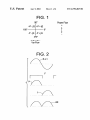
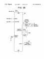
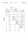
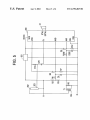
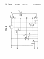
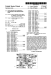
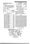
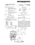
US006370483B1
(12) United States Patent
(10) Patent N0.:
Beckwith
(54)
(76)
(*)
US 6,370,483 B1
(45) Date of Patent:
*Apr. 9, 2002
SYNCHRONOUS LINEAR MACHINE FOR
4,871,971 A
*
PROTECTIVE RELAYING
5,315,527
A
*
5/1994
Beckwith . . . . . . . .
. . . . ..
5,544,064
A
*
8/1996
Beckwith . . . . .
. . . .. 700/293
Robert W. Beckwith, 2794 Camden
57646512 A
*
7/1997
Beckwlth ~ ~ ~ ~ ~
~ ~ ~ " 323/257
Rd‘, Clearwater, FL (Us) 337594007
5,774,366 A *
Inventor:
Notice:
Subject to any disclaimer, the term of this
10/1989 Jeerings et a1. ............. .. 361/47
6/1998 Beckwith ................... .. 702/64
OTHER PUBLICATIONS
patent is extended or adjusted under 35
_
U_S_C_ 154(k)) by 0 days_
Phadke & Thorp, Computer Relaymg for PoWer Systems
Thi_5 Pawnt is Subject to a terminal disClalmer-
John Wiley and Sons, NeW York, 1988 pp. 123—129.*
Altuve, DiaZ, and Vasquez, Fourier and Walsh Digital Fil
tering Algorithms for Distance Protection, IEEE Transac
tions on PoWer, vol. 11, No. 1, Feb. 1996, pp. 457—462.*
(21) Appl' NO‘: 09/303’449
(22) Filed;
702/72
HarloW, J.H., A Multifunction Protective Relay for the
May 3, 1999
Cogeneration Industry, IEEE Computer Application in
PoWer, vol. 3, No. 4, 1990, pp. 25—30.*
Yalla, Murty V.V.S., A Digital Multifunctional Protective
Relay, IEEE Transactions on PoWer Delivery, vol. 7, No. 1,
Related US‘ Application Data
(60) lgg‘gsional application NO‘ 60/089271’ ?led on Jun‘ 15’
'
1992, pp. 193—201.*
(51)
Int. Cl.7 ...................... .. G01R 19/00; G01R 25/00;
(52)
US. Cl. ........................... .. 702/65; 702/64; 702/72;
(58)
_
’
Field of Search ............................. .. 702/64—66, 71,
HOZH 3/00
* cited by examiner
361/35' 361/79
.
702/72, 73, 70_74; 361/35, 47, 65, 79;
327/2, 3, 15, 141, 101, 104; 700/286, 292—294;
.
(74) Attorney, Agent, or Ftrm—Leo J. Aubel
(57)
ABSTRACT
323/207, 211
(56)
.
Primary Exammer—Bryan Bui
-
Synchronous programs give increased sampling rates of AC
References Cited
signals and provide AC phasors yielding fast response to
undesired conditions.
U.S. PATENT DOCUMENTS
4,256,972 A *
3/1981 Wyatt et al. ................ .. 307/68
19 Claims, 6 Drawing Sheets
+5VDC
1
TpMPmn
VRH VDD
F|g.3B
F1
ANO
DATA
TO MP100
— F2
.35
4 AN1
F3
XTAL:lj12
ANZ
EXTAL
F4
ANS
CLK
—
OUT TOMP10O
PCO
Fig.3B
P01
Optional To
MP200
F5
AN4
,
P02
'5
I
N
|C
Pea
+9100 F11— F6
‘ ANS
.
— PC4
'6
N
I
Ma")
N
— P05
VRL
vss
U.S. Patent
Apr. 9, 2002
Sheet 1 0f 6
US 6,370,483 B1
FIG. 1
90°
Power Flow
+
180°
270°
+
-
Var Flow
FIG. 2
U.S. Patent
Apr. 9, 2002
Sheet 3 0f 6
US 6,370,483 B1
See FIg 4A LCI
VDD
100
/\/
From MC1<—- DATA
Optional
R | D'
eg‘jwe'r've
From MC1——- CLOCK IN
10!.
,
I
.
To
Re,'ayl g“ r- CIRCUIT
Drivel
1- BREAKER
N
BINARY *
D100
OUTPUTS _|_éfl/
~
BINARY
p51
l
—— I
N
‘
///
LEDs
D101 N'
INPUT
_|_
N
1 2
/~ 0
DATA
VSS
Isolated
RS232 PORT
U.S. Patent
85+
Apr. 9, 2002
_
Sheet 5 0f 6
US 6,370,483 B1
8> 1%
ww>
$2
.
.2»?Fz<.
.m
2%
.QEm swk
NEW
VI
E8
2a
W21
mom
Nol-A
E
To
2‘
:m8
mm8841>‘
U.S. Patent
Apr. 9, 2002
$116666 6 6f 6
US 6,370,483 B1
#56
r
mw>
1%
$2.
NEW
§\
vE
Eme
20
0 >?I
W21
82i
- Fz<6 EM
88é>
No -m
E
Q5
ANS
2
8
US 6,370,483 B1
1
2
SYNCHRONOUS LINEAR MACHINE FOR
PROTECTIVE RELAYING
completed While the phase angle betWeen the tWo sources is
Within a selected phase angle WindoW. The second criterion
This application claims the priority date of provisional
patent application Ser. No. 60/089,271 ?led on Jun. 15,
1998.
BACKGROUND OF THE INVENTION
It is the present practice of a BeckWith Electric Company
line of generator and transformer protective relays to sample
alternating current (AC) voltage and current Waves some
small number of times, such as 16 per cycle, and then use
10
operation does protect equipment from damage. In addition,
Fourier transforms to compute phasor quantities represent
ing fundamental components of the Waves.
Reference is made to the folloWing book and articles on
the present related state of the art:
as in protective relays that detect fault conditions, its opera
tion likeWise depends on a cycle by cycle measurement of
15
voltage and current Waves.
In making improvements over the present art, use is made
[1] Phadke, A. G. and J. S. Thorp, Computer Relaying for
PoWer Systems, John Wiley and Sons, NeW York, 1988,
pp. 123—129.
[2] Hector J ., Altuve F., Ismael DiaZ V. and Ernesto
?rst separates the motors from the ?rst source and then
makes a synchronous transfer When the isolated motor bus
falls behind the second source by 360 degrees. The third
criterion of transfer is used if the motor bus voltage falls
beloW a selected value before the 360 degree point is
reached.
While a bus transfer device does not have the requirement
to trip a circuit breaker in order to interrupt a fault current,
it is classi?ed herein as a protective device since proper
herein of the folloWing inventions, all by the present
inventor, Robert W. BeckWith.
A) US. Pat. No. 5,315,527, METHOD AND APPARA
20
TUS PROVIDING HALF-CYCLE DIGITIZATION
OF AC SIGNALS BY AN ANALOG-TO-DIGITAL
VaZqueZ M., “Fourier and Walsh digital ?ltering algo
rithms for distance protection”, IEEE Transactions on
CONVERTER, describes apparatus and methods for
PoWer, vol. 11, No. 1, February 1996, pp. 457—462.
[3] HarloW, J. H., “A multifunction protective relay for the
cogeneration industry”, IEEE Computer Application in
PoWer, vol.3, No.4, 1990, pp.25—30.
sensing positive half cycles of AC signals.
25
B) US. Pat. No. 5,544,064, APPARATUS AND
METHOD FOR SAMPLING SIGNALS SYNCHRO
NOUS
WITH
ANALOG-TO-DIGITAL
CONVERTER, describes apparatus and methods use
[4] Yalla, Murty V. V. S., “A digital multifunction pro
tective relay”, IEEE Transactions on PoWer Delivery,
ful for obtaining digital samples of AC Waves synchro
vol.7, No.1, 1992, pp.193—201.
Making use of inventions as found in US. Pat. No.
nous With free running analog to digital converters
30
5,224,011, MULTIFUNCTION PROTECTIVE RELAY,
one typical product, model M-4320 manufactured by the
BeckWith Electric Company, uses a digital signal processor
(DSP) running at some 80 megabits per second, to compute
(ADCs).
C) US. Pat. No. 5,774,366, AMETHOD FOR OBTAIN
ING THE FUNDAMENTAL AND ODD HARMONIC
Fourier transforms of the Waves as digital samples are taken. 35
The results are fed to a dual ported random access memory
Where they are available to a host processor. The host
COMPONENTS OF AC SIGNALS, describes methods
for obtaining the fundamental component and odd
harmonics of half Wave AC signals.
D) US. patent application Ser. No. 710,816, TWO WAY
PACKET RADIO INCLUDING SMART DATA
BUFFER AND PACKET RATE CONVERSION, the
inventer herein, ?led on Sep. 23, 1996 describes appa
processor, operating at 10 megabits per second, uses the
results to compute the existence of electrical fault conditions
and to output commands for tripping circuit breakers so as
to quickly remove electric poWer feeding faults.
In the M-4320 it is necessary to use analog component
anti-aliasing ?lters to prevent errors due to problems intro
duced by the use of a small number of digital samples of the
40
ratus and methods of communicating synchronously
With the poWer frequency as useful in the present
invention.
The present invention combines use of the half Wave
AC Wave. Since the electronic circuit is connected to earth 45 technology of US. Pat. No. 5,315,527 together With the
synchronous linear technology of US. Pat. No. 5,544,064
and methods for obtaining the fundamental component and
ground, transformers must be used for all current and
voltage inputs.
odd harmonics of a half Wave AC signal of US. Pat. No.
Another BeckWith Electric Company product line makes
5,774,366 in reducing the hardWare and softWare require
use of inventions contained in US. Pat. No. 4,310,771
METHODS FOR TRANSFERRING POWER IN A SYN
CHRONOUS MODE TO A MOTOR BUS, US. Pat. No.
4,256,972 POWER TRANSFER RELAY and US. Pat. No.
4,311,919 TRANSFER LOGIC CONTROL CIRCUITRY
In products based on the above referenced US. Pat. Nos.
4,310,771, 4,256,972 and 4,311,919 a ?rst analog device is
ments While at the same time increasing the operating speed
of devices useful in AC electric poWer apparatus. Means of
communicating betWeen devices using the present invention
and any of the many protocols in use at the time of Writing
of this application are provided by the inventive means and
55
methods by reference US. patent application Ser. No. 710,
used to develop information useable for the transfer of a
816.
motor bus from a ?rst source to a second source, not
US. Pat. No’s. 5,315,527, 5,544,064, 5,774,366 and US.
patent application Ser. No. 710,816 are incorporated herein
necessarily in phase With the ?rst, in a sequence of criteria.
A second combined analog and digital device uses the
by reference.
information to effect the transfer. Use of these devices
SUMMARY OF THE INVENTION
results in a large and expensive combination of equipment.
The transfer of motor busses is sometimes made manually
This invention utiliZes tables of sine and cosine functions
multiplied by digital samples of AC Waves to obtain, by
for operating reasons. At other times the transfer may be
initiated automatically due to the failure of a bus presently
in use.
The ?rst criterion used is called the “fast transfer” and
operates if calculations indicate that the transfer can be
65
cross correlation, the values of phasors for the Waves, thus
eliminating the need for Fourier transform calculations
required in many prior art devices. These phasors are
obtained one or more times per cycle of AC voltage and
US 6,370,483 B1
3
4
current Waves in order to determine output requirements,
ADC input, a squared Wave, F in FIG. 2, is created at MC1
binary inputs F1 through F6 of FIG. 3a. The square Wave
generally in the form of operation of solid state sWitches.
In a ?rst microprocessor, linear programs, using ?xed
identi?es positive and negative half cycles of the recti?ed
operating time loops, operate synchronously With micropro
AC Waves.
cessor ADCs. These ADCs produce digital samples in
matching loops and require no ongoing instructions from the
linear programs. A second microprocessor obtains the pha
contained in US. Pat. No. 5,544,064 referenced above.
Floating point arithmetic is not used. These programs run
sor information via a high speed synchronous data bus from
the ?rst microprocessor and computes results such as fault
clearing and motor bus transfer conditions. Use of linear
Programs are used in MC1 based on the inventions
continuously using no interrupts. By adding do-nothing
steps in program loops Written in assembly language, the
10
the result register of MC1. This provides the highest possible
digital sampling rate along With the longest possible com
putation time betWeen digital samples using any selected
programs loops matching those of the ?rst microprocessor
avoids data clashes betWeen the tWo microprocessors. Both
microprocessor programs run continuously Without the use
of interrupts.
Functions of the tWo microprocessors are combined into
15
MC.
The process is illustrated using a Motorola
20
MC68HC16Z1 microcontroller (a microprocessor having an
ADC). In reference to the Motorola M68HC16 Family
User’s Manual MC68HC16Z1UM/AD, Which is incorpo
rated herein by reference, one ?nds: (The page references
beloW are in the aforesaid Manual.)
a) The maximum system clock for the MC68HC16Z1 is
16.78 MHZ. Either a crystal (nominal frequency: 32.768
kHZ) or an externally generated signal can be used. (Page
one microprocessor for protection of single phase equipment
and for motor bus transfer.
Examples are given for use of the invention.
BRIEF DESCRIPTIONS OF THE DRAWINGS
FIG. 1 shoWs relations betWeen four quadrants of phasors.
FIG. 2 shoWs combination of monopolar ADC inputs With
logic inputs to determine four quadrant phasors.
FIGS. 3a and 3b illustrates a basic circuit for three phase
loop is completed just in time to ?nd a neW ADC result in
25
protective relays having three voltage and three current
1—1).
b) The analog-to-digital converter module (ADC) is a
unipolar, successive-approximation converter With eight
inputs.
modes of operation. It has selectable 8- or 10- bit resolution.
FIG. 4 illustrates a circuit With three voltage inputs useful
for motor bus transfer applications.
(8- is used in the illustration contained herein). (Page 6.1).
30
FIG. 5 shoWs single phase inventive protective relay
circuitry using “smart” three terminal fuses to interrupt
currents.
MC68HC16Z1UM/AD.)
FIG. 6 shoWs single phase inventive protective relay
circuits using small ground currents to cause ground fault
circuit breakers to interrupt currents.
The system clock must be divided by an integer number
of at least 8 to obtain an ADC clock frequency of 2,097,500
cycles per second. (Rounded off to 2.1 MHZ on page 6—14
and elseWhere of said referenced manual
35
c) As seen on page 6—15 of the referenced manual, an
ADC resolution of 8 bits is obtainable using 16 ADC clock
cycles conversion time per sample.
DETAILED DESCRIPTION OF THE
PREFERRED EMBODIMENTS
The invention is described hereinunder using presently
40
available semiconductor devices. General principles are ?rst
demonstrated and then examples of applications are shoWn
in Which selectable designer choices are illustrated. It is
anticipated, hoWever, that the general principles of the
invention Will be applicable using future devices not avail
able at the time of Writing of this document.
The invention is illustrated using selected Motorola
microcontrollers, MC1 of FIG. 3a and MC100 of FIG. 3b,
the illustrated examples of the inventive concepts given
beloW.
d) As seen on page 6—11 of the referenced manual, When
45
consisting of microprocessors having onboard analog to
the ADC is con?gured in Mode 7, continuous conversions
are performed on each of eight sequential input channels.
Note that mode 7 is useful When from ?ve to eight ADC
inputs are required.
processors MP means all of MC1 or MC100 except for the
ADC portions. MC1 operates synchronously along With
55
currently available from Motorola.
Alternating current (AC) Waves, voltage E and current I
of FIG. 2, are recti?ed, shoWn as AN in FIG. 2, and fed to
inputs ANO through AN5 of an ADC preferably located on
a microcontroller 1 (MC), see FIG. 3a. Further use is made
of the nature of a unipolar ADC to act as a nearly perfect
recti?er as in described in reference US. Pat. No. 5,315,527.
A problem introduced by the full Wave recti?er is that the
polarities of the original E and I Waves are lost, as illustrated
by Wave AN of FIG. 2. To overcome this loss and to form
a true four quadrant phasor detector from the single unipolar
the ADC is con?gured in Mode 6, continuous conversions
are performed on each of four sequential input channels.
Note that mode 6 is useful When four or less ADC inputs
are required.
e) As seen on page 6—11 of the referenced manual, When
digital converters (ADC)s. References hereinunder to micro
MC100. MC100 need not have an ADC, hoWever it is the
same device as MC1 in the illustrative circuits of FIGS. 3a
and 3b since a matching MC Without an ADC is not
Note that in reference US. Pat. No. 5,315,527, it Was
found that greater than 8 bit resolution is obtainable from the
averaging of errors in the type of ADC used in this selected
microcontroller. Eight bit resolution is therefore chosen in
In Mode 6, conversions in each channel occurs every
16><4 or 64 clock cycles. At a clock frequency of 2.1 MHZ
the period is 1/2.1 or 0.476 microseconds Which multiplied
by 64 gives a conversion every 30.5 microseconds. Since a
60 HZ Wave has a period of 16,6666 microseconds, a sample
60
can be made every 16,666.6/30.5=547 digital samples per
poWer frequency cycle.
In mode 7 a similar computation gives one half the rate for
Mode 6 or 273 digital samples per poWer frequency cycle.
In applications using every ADC result, the microproces
65
sor portion of the MC has 16><8=128 cycles, for addressing
the ADC result register and making phasor computations.
Selectively, by a designers choice, this number can be
US 6,370,483 B1
5
6
increased by a multiplier of 3, giving 384 clock cycles for
sor component magnitudes are passed to MC2 as sums of
the sampling and computing time, for applications requiring
products. The square roots of these sums are computed in
additional computing time. Increasing by a factor of three
MC2 producing the real and imaginary components of
causes the digital samples to precess among the inputs so
that all are accessed in sequence With intervening digital
phasors. Selectively these components are converted to
polar form by computing the square root of the squares of
samples ignored. A factor of ?ve may also be used, further
increasing the available computing time but further reducing
the number of digital samples per poWer frequency cycle.
Do-nothing steps are added to computation times to make
them synchronous With the ADC conversions.
The identity of the ADC channels used in the computation
is thus inherent in the Writing of the microprocessor 1
the real and reactive terms as the magnitude With an angle
Whose sine is real component/reactive component.
Phasor calculations for various protective relay and motor
bus transfer applications are Well knoWn and Will not be
10
further described herein. Higher level languages may selec
tively be used in MC100, FIG. 3b.
Integrals of digital samples multiplied by sine and cosine
program and no further addressing means are required. It is
functions represented by binary values stored in tables are
necessary, hoWever, to initialiZe the program so as to iden
formed in a sequence lasting 360° of an AC input Wave at its
tify a chosen channel as a starting point. As a ?rst initialiZing
15 nominal frequency. The signs of these integrals determine
alternative a clock on board MCI is used to reinitialiZe the
the polarity of the phasor components. A sum is calculated
computation, say every second, in order to assure proper
for one per unit voltage or current sine Waves and entered as
identity of the digital samples.
constants in the program. Division of measured integrals by
As a second initialiZing alternative the computation is
these constants produces phasors normaliZed in magnitude
reset by the ?rst program after every four channels are
computed When in Mode 6 and after every eight channels are
computed When in Mode 7. In theory the time taken to reset
the program may cause an error in the time sequencing of the
to per unit terms.
FIG. 3a gives examples of circuits used to process three
voltage Waves along With examples of circuits used to
process three current Waves.
digital samples, hoWever the reset is accomplished at the
The voltages are shoWn having a common neutral (N)
highest MP1 clock frequency and is so short as to greatly
minimiZe the error. The advantage of this second alternative
is that accidental program interruptions by electrical tran
input connection. External potential transformers (PTs) are
used as required for some inputs so as to input to this
common connection N. Selectively printed circuit boards for
the circuit of FIG. 3a use foils largely covering the outer
sients are more quickly corrected.
The ADC of MCI of FIG. 3a operates by charging a
sampling capacitor to the analog input for tWo cycles of the
ADC clock. At the highestADC clock frequency of 2.1 MHZ
this sampling time is approximately tWo microseconds. This
is unchanged by the increase in computation time by use of
the aforementioned multipliers of three or ?ve. The response
time of potential transformers and current transformers
providing the E and I Waves must be such that a Wave Will
30
four or more layers.
Digital Wave samples are processed by ?rst multiplying
each of a series of samples by numbers from a table
35
during 2 microseconds.
40
mined by sensing the appropriate F input just before a digital
sample conversion starts. For example, binary input F1 is
read just before a conversation starts for an input at ANO.
The Use of Cross Correlation
Cross correlations are made betWeen selected digital
samples and tables of sine and cosine functions to measure
corresponding to values of a sine function from Zero to 360°.
The resultant products are summed just folloWing compu
not change more than the desired amplitude resolution
Square Waves, F, fed to MC1 terminals F1 through F6, are
high When the corresponding Wave is positive and loW When
they are negative. The sign of any digital sample is deter
sides of the boards. These are connected together by plated
holes and connected externally to neutral. This effectively
shields circuitry carried on inner layers of the boards having
tation. This gives a ?rst sum value With its sign related to the
real or P component of a phasor. A second sum is formed in
a similar manner using numbers representing 360° of a
cosine function and gives a result related to the imaginary or
Q component of a phasor. Phasors are thus located in one of
the four quadrants of FIG. 1.
It may be most convenient for a programmer to provide a
table of alternating sine and cosine values so as to enable
45
computation of the P and Q results in less computation
cycles.
In some applications, measurement of the third and ?fth
magnitudes of fundamental components of Waves and pha
sors components of related harmonics, said phasors using
said fundamental components as phase references.
harmonics of the poWer frequency may be required. This is
provided by multiplying the digital samples by stored tables
of the harmonic and summing the result as covered in more
detail in reference US. Pat. No. 5,774,366. As described in
Cross correlation is de?ned as:
this patent, use of ?rst one and then a second table gives
harmonic components 90° apart, thus providing phasors for
the harmonics.
Where C is a correlation number and “a” and “b” are
functions each represented by a series of digital values.
55
case “a” is any monotonic function of a variable such
as time and “b” is another monotonic function of the
same variable. The cross correlation gives the similar
are completed to a second MC100, see FIG. 3b. This is
60
ity of the tWo functions for Whatever reason.
As used herein, functions “a” and “b” are limited to the
case of sine Waves in time With related harmonics. The
denominator is generally not used in this application.
In order to minimiZe the computation time by MP1 and
thereby maximiZing the number of samples per cycle, pha
These phasors are produced in a ?rst MC1 at a rate of one
set for each cycle of the poWer frequency. These sets of
phasors are transferred over the high speed synchronous
busses provided by port E of the MC68HC16Z1 as the sums
Each sum, 2, is computed over the range of the values
of “a” and “b”. It is generally required that “a” and “b”
have the same number of sample values. In the general
preferably from the same family of devices as MC1 except
that MC100 need have no ADC. In practice, hoWever, it is
most convenient to use the same device, such as the
65
MC8HC16Z1, for both MCI and MC100.
A program in a second microprocessor contained in
MC100 makes computations using the phasors as inputs so
as to determine the desired overall device response to
changes in the phasors. Selectively programs for devices 1
US 6,370,483 B1
7
8
and 100 are held in programmable read only memory
(ROM) on board each device. Alternatively programs are
F1, F2, F3,F4, F5, F6 and F7, ADC outputs ANO, AN1,
AN2, AN3, AN4 and AN5, binary inputs PCO, PC1, PC2,
PC3, PC4 and PC5, crystal (XTAL) connections XTAL and
EXTAL, clock out (CLK OUT), together With tWo high
speed synchronous data connections DATA. Input direct
held in ?ash memory requiring additional chips and having
the advantage of being reprogrammable through communi
cation ports.
Local communications is not shoWn but is furnished using
current poWer 12 VDC connects to voltage regulator 2
means such as insulated RS232 ports 102 of FIG. 3b
supplying 5 VDC to VDD. Upper ADC voltage limit VRH
connectable to portable computers for program entry and for
modi?cation and setting of setpoints as required. One alter
nate method of communications is by tWo Way infra red
ports. A second alternate method of communications is by
radio as described in US. patent application Ser. No. 710,
816 referenced above. Any of the three methods provide
desirable isolation of the communications inputs and the
input connections N. Minimal communications as to the
is provided by precision regulator 3 and loWer ADC limit
VRH is provided by connection to neutral N.
Three phase AC voltages EA, EB and EC each connect to
identical signal conditioning circuitry only one of Which Will
be described in detail. EA connects to neutral N via resistors
15
status of devices containing MC1 and MC100 is provided by
light emitting diodes (LEDs) D100 through D101 as selec
tively activated by input pushbutton sWitches PB1 con
nected from MC1 binary inputs to neutral Ns (See FIG. 3b).
during the positive portion of the cycle of voltage E and
through diode D2 to neutral during the negative portion of
the cycle. This produces a square Wave voltage into MC
It is Well knoWn from applications of reference US. Pat.
No. 5,315,527 that approximately four bits of added reso
input F1 further sharpened in squareness by the binary
lution in the magnitude of phasor components Will be
obtained When summing a large number of ADC samples
due to cancelling of the errors in the siZes of the capacitors
used in the ADC conversion process. With the ADC set for
8 bits resolution, 12 bits resolution are obtained.
The resolution is further eXtended for current Waves, if
R2 and R3 producing signal E of FIG. 2. Signal E is a
voltage chosen not to exceed the linear range of ADC input
ANO. Resistor R1 supplies current through diode D1 suf?
ciently loW as not to effect the regulator 2 output voltage
nature of the MC1 input so as to be accurately read by the
?rst synchronous program Within MC1. Transistors Q1 and
Q2 form a double emitter folloWer and gate 13 for positive
25
going analog voltage inputs. One input to this and gate, f+,
is formed during the positive portions of voltage E by
Resistor R25 and Diode D3. A second input, f—, is from an
necessary, by program sWitching of CT burdens R8 and R9
using sWitches 7 and 8 of FIG. 3a as driven by binary
analog polarity inverter consisting of operational ampli?er
outputs PC1 and PCO of MC1. Additional burdens are
during the negative going portions of voltage E. Circuitry 5
10 and resistors R4 and R5 forming positive inputs to ANO
selectively included and sWitched as required by application
and 6 having inputs EB and EC respectively are eXact
conditions. Alternatively programmable gain ampli?ers (As
duplicates of the circuitry having inputs EA and Will not be
shoWn in reference prior art US. Pat. No. 5,224,011) can be
used in the current signal paths to the ADC With the
described in further detail.
Three phase AC currents IA, IB and IC each connect to
ampli?er gain set by outputs from MC1.
35
In order to make most efficient use of the 16 bit processing
With the microprocessor used for illustration, the ADC may
preferably be set for 8 bit resolution and tables used having
8 bit numbers. This produces 16 bit products most ef?ciently
handled by the 16 bit processor. Multiplying the conversion
time of 16 ADC microprocessor clock cycles by the differ
leaving as current IA‘. CT T1 output currents I1 and I2 ?oW
serially through resistors R10 and R11 With center points of
said resistors connected to neutral N. Transistors Q3 and Q4
form a double emitter folloWer “and” gate 13 for positive
going analog current inputs AN (of FIG. 2) connected to
ence of 8 gives 8 * 16 or 128 cycles of computation cycles
as the available length of each computation time betWeen
ADC input AN3. Positive portions of currents I1 ?oW from
neutral N through diodes D11 and through resistors R10
digital samples.
While phasor results once per cycle may be adequate for
selected applications, additional sets may be produced by
selectively starting sums at points during computation of the
identical signal conditioning circuitry only one of Which Will
be described in detail. Currents IA ?oW through primaries of
current transformers (CT) T1, entering as current IA and
45
forming voltage inputs f+to and gates 13. Positive portions
of currents I2 ?oW from neutral N through diodes D10 and
through resistors R11 forming providing inputs f- to gates
?rst sum described above. For eXample, a second set of sums
13. When current I1 ?oWs through diode D10 the voltage
started midWay during the computation of the ?rst set of
sums provides recognition of phasor changes in one half
drop sWitches the output of operational ampli?er 9 from loW
to high voltage quickly driving binary input F4 to a high
cycle of the AC Waves. Four sets of sums started at quarter
state thus providing an accurate detection of Zero crossings
cycle intervals provides recognition of phasor changes in
of current IA for reading by programs contained in MC1.
Circuitry 10 and 11 having inputs IB and IC respectively are
one quarter cycle of the AC Wave.
PoWer for the circuitry of FIG. 3a and FIG. 3b is shoWn
as supplied from a 12 Vdc bus With negative terminal
common to the equipment neutral bus. Selectively this is a
eXact duplicates of the circuitry having inputs IA and Will
55
12 volt lead acid battery With charger. Alternate voltages are
24 and 48 VDC. Alternatively 5 VDC is input from DC/DC
With full knowledge of the second program Which the
programmer Writes for MC100, the programmer plans the
programs using a tWo Way communications protocol that
avoids data clashes betWeen communications traf?c in the
converters from station batteries or secure AC control poWer
sources. In such cases, regulator 2 is not used.
The inventive protection provides a reduction in siZe and
a reduction in cost over the present art.
FIGS. 3a and 3b illustrate a circuit useful for poWer
tWo directions.
generator protection. Details for a device protective of
rotating three phase generators folloW hereinunder.
In FIG. 3a, MC1 has a 5 Vdc poWer input VDD and return
VSS connected to neutral input connection N, binary inputs
not be described in further detail.
Synchronous tWo Way communications is established
betWeen MC1 and MC100 as shoWn on FIGS. 3a and 3b.
Since the ?rst program in MC1 is Written by the programmer
65
The crystal 12 used to establish the clock rate for MC1
also provides a CLK OUT signal connected to MC100 to
establish the clock in MC100 in synchronism With the MC1
clock.
US 6,370,483 B1
9
10
Typical Applications
from a capacitor fed With positive charge through three
diodes connected to EP, EM and EN (these components not
shoWn). PoWer is thus available When any of the three inputs
EP, EB or EN is poWered. Regulator 2 converts the input dc
voltage to 5 Vdc. The 5 Vdc supplies microprocessor 300
The inventive apparatus and programming methods are
useful in three phase protection of rotating generators and
poWer transformers. Because of the loWer cost of equipment
using the invention, hoWever, typical applications are more
likely found in areas not presently served by present prac
tice. Several such uses are described in greater detail here
(hereinafter knoWn as MP300) supply terminal VDD and
upper voltage reference terminal VRH along With collector
inunder.
Motor Bus Transfer
TR302, TR303 and TR304 respectively). Terminal EP
Many motor bus applications, especially at industrial
sites, do not justify the higher costs of prior art equipment
using US. Pat. Nos. 4,310,771, 4,256,972 and 4,311,919
of transistors 302, 303 and 304 (hereinafter referred to as
10
cited hereinabove and simpli?ed inventive devices are appli
cable.
brings voltage Waves from the present bus to a voltage
divider consisting of resistors 305 and 311. Divided voltage
is fed through resistor 308 to the base of TR302. Diode 317
is connected from TR302 base to neutral effectively limiting
the negative half cycle of AC voltages to approximately-0.7
volts from TR302 base to emitter. TR302 emitter draWs
Three sets of voltage inputs are used, one to a motor bus
and one each for tWo alternate sources of poWer. These tWo 15 current through resistor 314 during positive AC half cycles
and provides positive half cycles of voltage Waves to MP300
analog to digital converter (ADC) input ANO. Terminal EM
supply busses are referred to as the present bus, “P”, and the
next bus, “N”. In general the role of the tWo supply busses
alternates betWeen P and N With each poWer transfer.
brings voltage Waves from the motor bus to a voltage divider
be from the detection of a problem on the P bus. In either
case, breakers are opened removing the motors from the P
bus.
consisting of resistors 306 and 312. Divided voltage is fed
through resistor 309 to the base of TR303. Diode 318 is
connected from TR303 base to neutral effectively limiting
the negative half cycle of AC voltages to approximately —0.7
While three phase protective relays require measuring full
volts from TR303 base to emitter. TR303 emitter draWs
cycles of voltage and current Waves, motor bus transfer
current through resistor 315 during positive AC half cycles
and provides positive half cycles of voltage Waves to ADC
Initiation of a motor bus transfer may be manual or may
relays do not involve determination of fault currents but are
initiated by the detection and interruption of motor bus faults
and other motor related problems by other equipment. This
other equipment then initiates a bus transfer.
Costs are reduced by combining phasor measurements in
positive half cycles of voltage Waves With transfer calcula
tions during negative half cycles. FIG. 4 illustrates a circuit
useful in transferring motor busses from one supply to
another.
25
effectively limiting the negative half cycle of AC voltages to
approximately —0.7 volts from TR304 base to emitter.
TR304 emitter draWs current through resistor 316 during
positive AC half cycles and provides positive half cycles of
The voltage magnitudes of inputs EP (present bus
voltage), EM (motor bus voltage) and EN (next bus voltage)
are measured during positive half cycles using apparatus and
methods described by reference US. Pat. No. 5,315,527.
The relative times betWeen the three inputs is determined by
microprocessor counters measuring times from the ?rst
voltage Waves to ADC input AN2. Crystal 12 is connected
to MP300 terminals XTAL and EXTAL providing control of
35
the MP300 bit rate. MP300 binary output BO closes a
contact in output circuit 301 using Well knoWn circuitry not
otherWise shoWn in detail. Negative supply N is connected
to MP terminal VSS as is the ADC voltage reference loW,
VRL.
non-Zero sample of one Wave to the ?rst nonZero sample of
While FIG. 4 illustrates a most economical use of a single
another Wave.
microprocessor it is to be understood that additional micro
processors may be required to accommodate other than the
most simple conditions for motor bus transfer.
The difference betWeen EP and EM is expected to be Zero
until a binary signal at IT, from an external protective
device, signals initiation of a transfer. This is generally a
contact from said protective device Which also trips a circuit
breaker betWeen the motor bus and the present bus. The
change in time betWeen EP and EM is compared to the time
betWeen the EP and EN and the time of synchronism of the
input AN 1. Terminal EN brings voltage Waves from the neW
bus to a voltage divider consisting of resistors 307 and 313.
Divided voltage is fed through resistor 310 to the base of
TR304. Diode 319 is connected from TR304 base to neutral
Dispersed Generation (DG)
45
The folloWing single phase devices use a single micro
processor for both phasor measurement and phasor compu
tation for abnormal condition determination. This is accom
motor bus and neW bus is predicted so as to initiate closing
plished by measuring phasors during positive half cycles of
of a breaker betWeen the motor and neW bus at an advance
input AC Waves and determining abnormal conditions dur
ing times Where both voltage and current Waves negative.
This results in greater numbers of digital samples of Waves
time equal to the closing time of the breaker about to be
closed. These time predictions are made With use of a model
of the nonlinear change in the motor bus speed With time.
This type of close is knoWn as “synchronous transfer”.
If the determination of EP-EB just after receiving IT is
less than a selectable amount, the breaker is closed imme
diately in What is knoWn as “fast transfer”.
The magnitude of the motor bus voltage is continuously
being taken during said positive half cycles thus yielding
greater accuracy of phasor components. All computation is
done in the negative half cycles.
An inventive device, not shoWn in detail herein, provides
55
compared to a selectable undervoltage limit and the breaker
betWeen the motor and the neW bus is closed immediately if
the undervoltge limit is met. This is knoWn as “undervoltage
closing” and has the advantage that the motor bus in-rush
current is then less than the motors bus starting current if the
motors had been alloWed to come to a complete stop.
(neutral). This device poWer can be as simple as an auto
other source of dc voltage such as 24, 48 and 120 volt
batteries. Further selectively, regulator 2 obtains input power
supply poWer to improve poWer quality. Such generators
may furnish poWer during the ?rst part of each cycle When
many phase controlled loads have not yet turned on. They
may also furnish poWer during voltage dips or poWer
interruptions of, for example up to one second duration.
Using capacitors for energy storage, such devices are inca
pable of handling the magnitude of fault currents deliverable
from rotating synchronous generators. These generators may
In FIG. 4 device poWer is supplied by an external 12 volt
battery connected from terminal marked “12 Vdc” to N
mobile battery With charger. Selectively the supply is any
backup disconnection of electronic generators intended to
65
have internal means for disconnection upon determining
factors indicating such a disconnection is necessary. For
safety reasons hoWever, some users require said backup
devices duplicating the protective disconnection contained
in the poWer quality generator.
US 6,370,483 B1
11
12
5) Providing easy user programmability of devices using
the inventive technology.
6) LoWer cost apparatus for high speed clearing of AC
Dispersed solar and other small sources of electrical
energy are used in increasing numbers in homes and small
businesses. These are generally single phase, supplying
some but not alWays all of the buildings requirements.
poWer fault conditions.
A safety requirement may be for devices disconnecting
(7) LoW cost means for preventing loW energy single
such sources so as to permit maintenance Work on nearby
phase dispersed generators from backfeeding danger
outside lines When these lines become disconnected from an
electric poWer system.
Fuses are being developed that Will bloW in normal
fashion With through current. They Will also bloW With the
ous voltages to poWer lines When the lines become
disconnected from poWer netWorks.
What I claim is:
injection of a small current into a third terminal. They are not
unlike ground fault circuit breakers except for requiring
1. Amethod for using ?rst and second microprocessors to
measure and process phasors of three phase AC Waves, the
replacement once bloWn. The three terminal fuses have the
advantage of being of selectable current rating for use in a
common receptacle. In addition devices such as described
hereinunder may be installed outside of buildings under the
method consisting of the steps of:
a) storing tables of values of sine and cosine functions in
said ?rst microprocessor,
b) sending positive recti?ed half cycles of said AC Waves
control of line maintenance personnel for their protective
to unipolar analog to digital converter (ADC) inputs
provided by said ?rst microprocessor,
use.
FIG. 5 illustrates a circuit for sensing a single phase
voltage from hot AC input, H, to neutral, N, and AC
dispersed generation current input DG. Three terminal fuse
202 is as described in the previous paragraph. Microproces
sor 200 computes voltage magnitudes during positive half
cycles and current phasors using the voltage as reference.
c) forming square Waves from said AC Waves With ?rst
20
provided by said ?rst microprocessor,
Current DG is connected so as to generally be in phase With
the voltage H leaving time for tripping calculation When
25
both voltage and current Waves are negative. When a trip
condition is determined MP200 binary output F1 turns off
thereby measuring phasors of AC Waves.
into terminal 203 of three terminal fuse 202 causing said
fuse to bloW interrupting poWer to DG. Said fuse also bloWs
normally upon excessive DG current.
2. A method as in claim 1 further including the steps of:
a) communicating said sums of products to said second
Input AC current DG creates an AC voltage across current
microprocessor, and
b) determining outputs by computations in said second
transformer T1 secondary burden R8. This voltage is fed to
ADC input AN1 through an emitter follower circuit using
transistor Q3 and resistors R200 and R12. This acts as a Zero
35
microprocessor using said sums of products
thereby processing phasors of said AC Waves.
3. A method as in claim 2 Wherein said outputs are used
half Wave at input AN 1.
Resistors R2 and R3 divide AC voltages from H to N and
for clearing electric poWer faults.
4. A method as in claim 2 Wherein said outputs are used
provide an input for emitter folloWer consisting of R6, R7
and transistor Q2 With output connected to microprocessor
to transfer motor busses from one source of electric poWer
to another.
200 ADC input ANO. Diodes D3 and D200 suppress nega
5. A method as in claim 1 further including the steps of:
tive voltage half cycles thus protecting transistors Q2 and
Q3.
a) synchroniZing programs in said ?rst microprocessor
PoWer supply 201 converts AC voltages from HI to N to
5 vdc for MP200 and transistors Q2 and Q3.
Tripping conditions may include:
1) Reverse poWer ?oW.
e) combining results from said ADC With logic levels
produced by said binary inputs in forming sums of the
products of digital samples from said ADCs and values
taken from said tables of values
transistor Q10 permitting resistor R13 to feed a small current
crossing detector to place a rather perfect positive voltage
levels indicating positive half cycles and second levels
indicating negative half cycles of said Waves,
d) applying said square Waves to binary input inputs
With said ADCs, and
b) synchroniZing programs in said second microprocessor
45
With said programs in said ?rst microprocessor, and
c) using programs Written so as to avoid communications
data clashes.
6. Amethod for using a single microprocessor to measure
2) Under/over frequency.
3) Under/over voltage.
FIG. 6 illustrates a circuit similar to that of FIG. 5 except
and process phasors of single phase AC Waves, the method
consisting of the steps of:
a) inputting positive half cycles of voltage Waves from
that a ground fault circuit breaker (not shoWn) is used to
interrupt dispersed generation current. Voltage for said DG
devices are connected to an AC source H to neutral (not
?rst sources of electric poWer to ?rst ADC inputs
shoWn but generally externally connected to ground GND).
MP 200 output F1 drives transistor Q10 causing tripping
provided by said microprocessor,
b) inputting positive half cycles of voltage Waves from
ground current through resistor R13 to terminal GND upon
determination of tripping conditions. All other components
second sources of electric poWer to second ADC inputs
provided by said microprocessor,
function as described under FIG. 5, above.
Tripping conditions include those itemiZed under FIG. 5.
Advantages of this invention include:
1) Eliminates the need for dual ported RAMs and high
c) inputting positive half cycles of voltage Waves from
speed DSPs for determining and analyZing phasors of
d) calculating conditions for transferring said motor bus
motor busses to third ADC inputs provided by said
microprocessor,
AC Waves.
from one to the other of said ?rst and second sources of
2) Higher speed tripping of circuit breakers to clear faults.
3) Accurate measurement of the fundamental and har
monic phasors of each cycle of an AC Wave.
4) Matching and exceeding capabilities of analog circuitry
for analyZing AC waves.
electric poWer, and
e) providing bus transfer outputs as determined by said
65
calculations.
7. A method for using a single microprocessor for oper
ating disconnection devices for disconnecting single phase
US 6,370,483 B1
14
13
generators from power lines during abnormal conditions, the
method consisting of the steps of:
a) sending positive half cycles of voltage Waves to ?rst
b) means for producing square Waves representing said
Waves Whereby a ?rst level indicates positive portions
of said Waves and a second level indicates negative
ADC inputs provided by said microprocessor,
portions of said Waves,
c) means for applying said square Waves to binary input
terminals of said microprocessor, and
d) program means for combining results from said ADCs
b) sending positive half cycles of current Waves from said
small generators to second ADC inputs provided by
said microprocessor,
c) connecting said voltages and currents so as to generally
With logic levels produced by said binary inputs to form
be in phase,
four quadrant phasors.
16. Apparatus for measuring single phase phasors of AC
d) making calculations, during times When voltage and
current Waves are negative, for determining abnormal
voltage and current Waves comprising in combination:
conditions, and
e) operating said disconnection devices during said abnor
mal conditions.
8. A method as in claim 7 further including the step of
a) microprocessor means having onboard analog to digital
15
using microprocessor programs synchronous With said
converter (ADC) means,
b) program means for measuring amplitudes of said
voltage Waves during positive half cycles of said
Waves,
ADCs.
c) program means for measuring phasors of said current
Waves using said positive half cycle of said voltage
9. Amethod as in claim 8 including the step of conducting
a current to ground so as to open a ground fault circuit
breaker
Waves as phasor references, and
thereby interrupting the output of a generator associated
d) program means for processing said amplitudes and
With said breaker.
10. A method of using one microprocessor to measure and
phasors and determining outputs during time periods
process phasors of AC voltage and current Waves, the
method consisting of the steps of:
25
a) storing tables of values of half cycles of sine and cosine
When both voltage and current Waves are negative.
17. Apparatus as in claim 16 further comprising in com
bination:
a) ground fault circuit breaker means for interrupting
outputs of said apparatus, and
b) means for causing said outputs to provide current How
to ground thereby tripping said ground fault circuit
Waves in said microprocessor,
b) taking sums of products of samples of AC Waves and
values from said tables in positive half cycles of
voltage and current Waves,
breakers.
c) obtaining phasors by taking the square root of said
sums of products during times When both voltage and
18. A method for using ?rst and second microprocessors
to obtain and process phasors of three phase AC Waves, the
method consisting of the steps of:
a) storing tables of values of sine and cosine functions;
current Waves are negative, and
d) completing the processing of said phasors so as to
obtain desired results during said times
b) sending recti?ed half cycles of said three phase AC
thereby improving phasor accuracy by maXimiZing the
Waves to unipolar analog to digital converter (ADC)
inputs provided by said ?rst microprocessor;
number of samples taken.
11. Apparatus for measuring and processing phasors of
c) forming square Waves from said three phase AC Waves
AC voltage and current Waves comprising in combination:
a) ?rst microprocessor means having on board analog to
With ?rst levels identifying positive half cycles and
second levels identifying negative half cycles of said
digital converter (ADC) means,
b) said ?rst microprocessor means taking digital samples
of said AC Waves and continuously processing said
samples to obtain phasors of said AC Waves,
three phase AC Waves;
45
c) second microprocessor means receiving and processing
said phasors and determining outputs,
produced by said binary inputs provided by said ?rst
microprocessor in forming sums of the products of
digital outputs from said ADCs, and values taken from
d) synchroniZing means for operating said ?rst and second
microprocessors at the same clock frequency, and
e) tWo Way communication means for communicating
betWeen said ?rst and second microprocessors.
12. Apparatus as in claim 11 further including means for
synchronous programs in said ?rst and second microproces
sors having preplanned communications protocols so as to
eliminate data clashes in the tWo directions of data ?oW.
13. Apparatus as in claim 11 further including means for
providing outputs to clear poWer faults When so indicated by
said phasors.
14. Apparatus as in claim 11 further including means for
providing outputs to transfer motor busses.
15. Apparatus as in claim 11 further comprising in com
bination:
a) means of rectifying said AC Waves and applying as
positive half cycles to said ADCs,
d) applying said square Waves to binary inputs provided
by said ?rst microprocessor; and
e) combining inputs from said ADC With logic levels
said tables of values of sine and cosine functions
thereby obtaining full Wave phasors of AC Waves.
19. A method as in claim 18 further including the steps of:
55
a) taking said sums of products an interger number of
times per cycle of AC Waves,
b) starting said sums of products an integer number of
times per cycle of AC Waves,
c) transferring said sums of products at the end of AC
cycles, and
d) processing said sums of products and obtaining said
results and integer number of times per cycle
Whereby response times faster than one cycle are
obtained.