1
i re
dsh
UNIVERSITY OF HERTFORDSIRE
fo r
Faculty of Engineering & Information Science
ert
BACHELOR OF ENGINEERING DEGREE WITH
HONOURS IN
yo
fH
ELECTRONICS & ELECTRICAL ENGINEERING
rsit
Project Report
Un
ive
USB CONECTIVITY OF PC WITH DSP MODULE
Muhammad Fahd Jadoon
April 2005
1
i re
dsh
Chapter # 1
Introduction
fo r
1.1 Aim
ert
To develop a real time communication protocol that will enable to exchange data
between P.C and DSP module. While the DSP module will keep on performing its usual
normal tasks/ functions .It will not be interfered or disturbed during its tasks by the
developed communication protocol that is transferring data from DSP module to PC.
1.2 Objective
yo
fH
1. Visual Basic for programming on the PC to receive and study the data from DSP
module.
2. DSP programming in Assembly Language i.e. for development of DSP drivers to
communicate with the USB module.
3. To study communication protocol principles for data exchange in real time.
4. Development of interface between PC and DSP module.
1.3 History Of Communication
Un
ive
rsit
Communication is part of human life right from the start there have been different
methods in the world. But with the passage of time as the technology advanced the
method of communication also changed.
But in 21st century with the advent of micro processor the whole scenario changed
The data transfer became more and more easy.
First it was transfer from serial/ parallel port or access through data bases .but all these
have there limitations like when you transfer data via parallel port although its fast as
compared to data transfer via serial port. But you require Many lines like to transfer 8 bits
you need 8 lines and this is applicable only at room level practically for longer distances
its not possible similarly in serial communication it goes bit by bit.
So then came the USB it has got highest data transfer rate upto 8 million bits/second. It
appears as virtual comm. Port to the system when it is connected. Data is transferred like
in parallel port but only with one cable.
The communication through USB is great development in the industry .
2
i re
dsh
Chapter #2
D.S.P Module
ert
fo r
The architecture of a data acquisition system utilizing the processing capability of a DSP
chip has existed for many years. The ability to do this in a local loop in real time is
available today with chips such as the Texas Instruments’1 floating-point TMS320C6713.
The advantages of such an approach for real-time processing
are many. But also of great interest is the ability for users to stream fast data rates to a
host in an economical way. The new standard of USB2 2.0 allows high speed data
transfer between such a DSP peripheral or standalone and a host PC.
yo
fH
If such a DSP-based data acquisition system could use the highest accuracy data
acquisition capability available today, and still transfer data at rates up to 480 Mbps, it
would truly be a breakthrough. Current relative accuracy limits for data acquisition are
24-bit or 60 ppb. This combined with data rates as high as 100,000 measurements per
second would provide breakthrough performance. A system architect could use
such performance either in a local control loop or on a stream basis via the USB 2.0
communications link. This freedom of choice would solve many measurement challenges
in industrial systems. For example, such an embedded system could perform signal
processing and real-time control independently of the host or under the control of the host
processor.
rsit
Other key advantages of this type of system would be:
• Plug & play features of USB 2.0 provide a quick and easy way to have the data
acquisition system up and running.
• Galvanic isolation can be implemented to protect the host computer from ground loops
and voltage transients -- a capability not often found on data acquisition products.
Galvanic isolation also helps to adhere to the tough CE requirements of EN50082-1:1998.
• Programs can be downloaded via USB 2.0 to on-board memory or flash.
Un
ive
The ideal operation of this real-time data acquisition system would allow simultaneous
operation in real-time of all measurement subsystems at high throughput rates and high
accuracy. The TMS320C6713 floating - point DSP could read data from 24-bit sigma
delta A/Ds, write data to 24-bit sigma-delta D/As, do digital input/output control
operations, or use on-board 32-bit up/down counter timers, all simultaneously and in
real-time. Scalability of these operations would also be possible by adding system boards
with common clocks and triggers. Data would be either sent to the host using USB 2.0 or
shared between processes with on-board 50MB per second LVDS ports. An additional
benefit of the USB 2.0 communication mechanism would be that power or system
operation is available as part of the connector mechanism.
3
i re
2.1 DSP Board
Un
ive
rsit
yo
fH
ert
fo r
dsh
The ADMC401 PROCESSOR BOARD is a compact, highly flexible evaluation and
development board for the single-chip DSP-based high-performance motor controller, the
ADMC401. The ADMC401 motor controller provides the following significant features:
· 26 MIPS, Fixed-Point, 16-bit DSP Core.
· 2K X 24-Bit Internal Program Memory RAM.
· 2K X 24-Bit Internal Program Memory ROM.
· 1K X 16-Bit Internal Data Memory RAM.
· 14-Bit Address Bus and 24-Bit Data Bus for External Memory Expansion
· 8 Input, 12-Bit Pipeline Flash Analog to Digital Converter inputs with < 2ms total
conversion time.
· A Three-Phase, 16-bit, Center-Based PWM Generator.
· An Incremental Encoder Interface Unit with Companion Encoder Event Timer.
· 12 General Purpose I/O Lines, Configurable as Inputs, Outputs, Interrupt Sources or
PWM Trip Sources.
· An Internal Power-On Reset System (POR).
· A Two-Channel Event Timer Unit.
· A Peripheral Interrupt Controller.
· Two Synchronous Serial Ports.
· Two Variable-Frequency, 8-Bit, Auxiliary PWM Outputs.
· A 16-Bit Watchdog Timer.
· A General Purpose, Interval Timer with Prescaler.
Refer to the ADMC401 datasheet for a full description of all features of the ADMC401.
The ADMC401 PROCESSOR BOARD is intended as a compact, highly integrated
evaluation and software development platform for the ADMC401 controller. The
processor board permits access through a UART connection to the Motion Control
Debugger software that operates under Windows 95Ô or Windows NTÔ. The Motion
Control Debugger is used to download executable code, examine the contents of
registers, program memory and data memory, run executable modules, set breakpoints
and enable single-step operation.
The processor board is designed for compact size so that all relevant input and output
signals are brought to three connector headers underneath the board. The processor
board contains the following features and components:
· The ADMC401 Single-Chip DSP-Based Controller.
· External RAM that can be used to expand both the program and data memory xternally.
· A socket for a byte wide EPROM that can be used to boot load internal and/or external
program and/or data memory.
· A 12.96 MHz crystal and associated capacitors to provide the CLKIN frequency.
· A jumper to enable use of the internal power-on reset system of the ADMC401 or an
external reset provided by a push button switch.
· A socket for a serial memory device (ROM or E2PROM) that may be used for serial
boot loading on power up for stand alone operation.
· An isolated UART interface to the Motion Control Debugger. The signals are optically
isolated from the remainder of the processor board. The AD7306 is used to drive the
appropriate signals on the 9-way UART connector.
4
i re
fH
ert
fo r
dsh
· An input power supply connector that accepts +5V(VDD), ±5V (±AVDD) and GND.
The +5V is used to drive the digital circuits and the analog portion of the ADMC401. The
±5V supplies are used for the analog interface circuits of the processor board.
· An on board 5V to 5V dc-dc converter that provides an isolated 5V supply for the
UART interface circuit.
· Analog interface circuits that correctly offset the analog input signals to the ADC inputs
of the ADMC401. Eight independent analog interface circuits are included: one for each
ADC channel of the ADMC401.
· An on board precision 2.048V voltage reference using the REF191, that can be used to
provide the input reference for the ADCs of the ADMC401. The reference voltage is also
brought to the connector underneath the board.
· Jumpers that permit setting of the PWM polarity, enabling or disabling of the
PWMTRIP input and enabling or disabling the serial memory device in the
socket. Additional jumpers are included on the board to allow selection of either internal
or external voltage reference for use with the ADC system of the ADMC401.
· Three socket blocks underneath the processor board that permit access to all of the input
and output signals of interest. The three sockets comprise two digital sockets (IF1 and
IF3) and one analog socket (IF2).
2.2 FUNCTIONAL DESCRIPTION OF PROCESSOR
BOARD
yo
This section is intended as a functional description only of the major elements of the
board.
2.2.1 UART Interface
Un
ive
rsit
A UART interface to the Motion Control Debugger is provided on the ADMC401
PROCESSOR BOARD via a 9-way D-type connector (P1). In order to separate the
ADMC401 and any power conversion stage used in a complete motor drive system, the
UART interface is optically isolated from the remainder of the processor board.
The Motion Control Debugger communicates through serial port 1 (SPORT1) of the
ADMC401 using the DR1B and DT1 pins. In addition, the ADMC401 reset signal
(ICRESET) is sent to the UART interface to ensure that a processor board reset is
detected by the Motion Control Debugger. The three signals, DR1B, DT1 and ICRESET
are optically isolated using two HCPL0630 dual isolators (U4 & U5). The signals DT1
and ICRESET are considered as outputs as these signals are sent from the processor
board to the debugger. These signals are applied to one opto-isolator. Conversely, the
signal DR1B is considered as an input as it is received by the processor board. This signal
is isolated using the second isolator U4. The secondary supply for the optical isolators is
produced on the processor board by the NME0505S power supply (isolated +5V to +5V
dc-dc converter).
The ADMC401 PROCESSOR BOARD also contains an AD7306 transceiver that
converts the TTL signals to the appropriate ±10 V levels suitable for the UART
5
i re
dsh
connection to the PC. A standard PC serial cable may be used to connect from the 9-way
female socket of the processor board to the appropriate COM port of the PC.
The baud rate and COM port to be used on the PC may be set from the ADMC401 Comm
Config software that is part of the Motion Control Debugger.
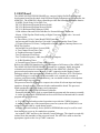
Figure 2.1
yo
fH
ert
fo r
A functional block diagram of the UART interface circuit is shown in Figure 2.1 . The
direction of the three signals is indicated in the figure. Refer to the full schematics at the
end of this document for the full circuit. Recall that the secondary supply for the optical
isolators and the AD7306 is derived on the processor board by the isolated dc-dc
converter, the NME0505S (U1).
rsit
2.2.2 Power On Reset Circuit
Un
ive
The ADMC401 contains an integrated power-on reset (POR) circuit that provides an
output reset signal from the ADMC401 on power-up and if the power supply voltage falls
below the threshold level. The ADMC401 may be reset using the internal power-on reset
circuit by connecting the POR pin to the RESET pin (jumper JP3 in 1-2 position) or
alternatively from an external source using the RESET pin (jumper JP3 in 2-3 position).
By pressing the S1 push button switch, the voltage level at the RESET pin is brought
below the threshold level. Resistor R9 and capacitor C26 limit the rise of voltage at
the RESET pin to allow the DSP core’s internal clock to stabilize. The RESET signal is
also fed to the UART interface, as described previously, to permit the Motion Control
Debugger to detect a system reset.
2.2.3 Serial ROM Interface
For normal program development, it is envisaged that the Motion Control Debugger
would be used to download executable code to the ADMC401 PROCESSOR
BOARD. However, as program development stabilizes, it may be required to operate the
processor board in a stand-alone mode in the target application. For this
6
i re
ert
fo r
dsh
reason, the processor board contains an 8-pin DIP socket (U7) for installation of a serial
memory device that can be used to boot load the program and data memory RAM of
the ADMC401.Either a one-time programmable serial ROM device, such as the
XC1765D Xilinx, or electrically erasable devices such as the AT17C65 E2PROM from
Atmel or the 37LV65 from Microchip are recommended. These devices provide
sufficient capacity to boot load the entire internal program and data memory space of the
ADMC401. If larger areas of memory must be boot loaded, compatible higher capacity
serial memory devices must be chosen (i.e. XC17128D, AT17C128 or 37LV128 or
higher). In all cases, the application executable file can be converted to a form suitable
for the serial memory devices using the MAKEPROM utility that is installed as part of
the Motion Control Debugger. For both memory devices, a three-wire connection to
SPORT1 of the ADMC401 is used.
2.2.4 Analog Interface
yo
fH
The ADMC401 PROCESSOR BOARD permits up to eight analog inputs to be fed from
the User Interface Connector, IF2A (pins 1 to 8), to the eight ADC channels of the
ADMC401. All eight analog inputs at the IF2AUser Interface Connector may range from
-2V to +2V. A Gain Calibration input may also be fed from pin 9 of the IF2A connector
to the Gain pin on the ADMC401. There is a separate interface circuit for each of the
eight ADC channels of the ADMC401 included on the processor board. These analog
interface circuits convert the nominally ±2 V signals at the IF2 interface connector
to signals centered on the ADMC401 reference voltage level (either the internally derived
2.0V level or the externally provided 2.048V level). The analog interface circuits,
consisting of high-performance operational amplifiers and precision resistor networks,
effectively offset the analog inputs by the reference voltage level.
Un
ive
rsit
Three AD8044 quad operational amplifiers are used (U8, U9 & U11) for the analog
interface and are configured as summing unity-gain stages. U8 is used to interface the
VIN0, VIN1, VIN2 and VIN3 analog inputs. U9 is used to buffer the VIN4, VIN5, VIN6
and VIN7 inputs. The G input is also level shifted and buffered in the same way using
one operational amplifier of U11. This is applied to the GAIN compensation input pin of
the ADMC401. Precision 10 kW resistor networks (RN1 – RN5) are used for input and
feedback resistors to ensure accurate gain matching of all channels. In addition, 270 pF
feedback capacitors are used to provide simple low-pass filtering with a 59kHz cut-off
frequency on all analog inputs.
The analog inputs are applied to the ADMC401 in a single-ended fashion, so that the
inverting inputs to the sample and hold amplifiers of the ADMC401 (ASHAN
and BSHAN) are connected to a buffered version of the reference voltage. A
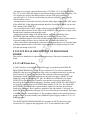
representation of the analog interface circuit for one of the ADC channels is shown in
Figure 2.2.As can be seen in the schematics at the end of this document, each analog
input stage also contains a small RC filter at the operational amplifier output.
7
i re
dsh
fo r
Figure 2.2
ert
2.2.5 Reference Voltage Generation
fH
The ADMC401 PROCESSOR BOARD contains an external voltage reference, the
REF191 (U10) that can be used to provide a precise 2.048V output. The evaluation
board can be configured to operate from either the internal (ADMC401 generated) or the
external voltage reference. Two jumpers control the selection of either internal or external
voltage reference.
rsit
yo
Jumper JP1 can be used to tie the SENSE pin of the ADMC401 to either the AVDD or
GND levels. Connecting SENSE to AVDD (JP1 in position 1) selects external voltage
reference operation. In this mode, the ADMC401 accepts an input voltage reference at the
VREF pin. In order to connect the external voltage reference to the ADMC401 on the
evaluation board, it is necessary to insert the JP7 jumper. This connects the external
voltage reference from the REF191 device to the VREF pin of the ADMC401. The signal
is also buffered (in one operational amplifier of U9) and used to level shift the applied
analog signals on the IF2 connector (as well as being connected to the ASHAN and
BSHAN inputs to the sample and hold amplifiers).
Un
ive
In order to operate with the internally derived voltage reference of the ADMC401, the
JP1 jumper must be tied in position 3 so that the SENSE pin is connected to REFCOM
(=GND). Additionally, the jumper JP7 must be left open. The ADMC401 provides a 2V
reference at the VREF pin that is buffered and applied to the ASHAN and BSHAN
inputs. The buffered VREF signal is also used in the level shifting circuitry The JP1
jumper has a third setting that permits the SENSE input to be tied to the VREF input.
This setting is not permitted.
In summary the appropriate settings for the jumpers JP1 and JP7 for internal and external
voltage reference
operation are:
INTERNAL Reference: JP1 in position 3, JP7 open
EXTERNAL Reference: JP1 in position 1, JP7 closed
In addition, the reference voltage level is buffered (opamp U11A). Additionally, the
voltage reference at the VREF pin of the ADMC401 is fed to the analog interface
8
i re
dsh
connector (pin 15 IF2A), underneath the processor board, where it can be used by
external circuitry. However, it is recommended that this signal be buffered prior to use by
any other circuitry.
2.2.6 External Memory Interface
yo
fH
ert
fo r
Provision is made on the processor board to expand both the program and data memory
externally to the ADMC401. There are three sockets (U12, U13 and U14) on the
processor board into which external RAM chips may be inserted. The processor board is
designed to operate with CY7C199 memory devices from Cypress or AS7C256 memory
devices from Alliance. The external memory is capable of zero wait state operation. The
three external memory chips are each arranged as a 32K x 8- bit memory array. When
connected in this way, the lower 16K is recognized as data memory and the upper 16K is
recognized as program memory. The selection is made by using the data memory select
(DMS) strobe as the upper address line to the memory devices. Of course, not all of
this space is available because areas of the external memory devices whose addresses are
identical to the internal memory space of the ADMC401 are unused on the external
memory chips. The three memory devices (U12, U13 and U14) are used by external
program memory, where U12 provides the low byte (D0-D7), U13 provides the middle
byte (D8- D15) and U14 provides the high byte (D16-D23) of the external 24-bit program
memory word. For external data memory accesses, only U13 and U14 are used since the
16-bit data memory word is read/written on data lines (D8-D23).
rsit
These external RAM chips provide an additional 12K x 24-bits of external program
memory RAM. This program memory block is arranged as one contiguous address
space starting at address 0x1000. Program memory read or write accesses in the address
range 0x1000 to 0x3FFF will access this external memory.
Un
ive
The following signals are all brought, directly from the ADMC401, to the User Interface
Connector, IF1, for easy access and external expansion, if required.
· The address lines (AD0 to AD13)
· The data lines (D0 to D23)
· The memory select lines ( BMS , DMS , PMS )
· The read/write strobe lines ( WR , RD )
· The bus request/grant control lines ( BGH , BG , BR )
· The powerdown pins ( PWDACK , PWD )
· The mode select pins (MMAP, BMODE)
9
i re
fH
ert
fo r
dsh
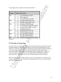
The settings of these jumpers are described in Table 2.1.
yo
Table 2.1
2.7 Interface Connectors
Un
ive
rsit
In order to create as compact an evaluation and development board as possible, all input
and output signals are brought to three interface connectors underneath the processor
board. Two connectors (IF1 and IF3) are dedicated to digital signals and the third (IF2) is
reserved for analog signals. This three connector interface will be used in future
processor boards for future motion control products from Analog Devices. Therefore,
many of the pins on the connectors for the ADMC401 PROCESSOR BOARD are
unconnected (n/c). These pins are reserved for other functions in future products.
Interface connectors IF1 and IF3 are both 3-way by 30 pin connectors. Connector IF2 is
3-way by 24 pins. The exact connections to this interface may be seen in the schematics
at the end of this document.
10
i re
dsh
Chapter # 3
UART
fo r
The Universal Asynchronous Receiver/Transmitter (UART) controller is the key
component of the serial communications subsystem of a computer. The UART takes
bytes of data and transmits the individual bits in a sequential fashion. At the destination, a
second UART re-assembles the bits into complete bytes.
ert
Asynchronous transmission allows data to be transmitted without the sender having to
send a clock signal to the receiver. Instead, the sender and receiver must agree on timing
parameters in advance and special bits are added to each word, which are used to
synchronize the sending and receiving units.
yo
fH
When a word is given to the UART for asynchronous transmissions, a bit called the "Start
Bit" is added to the beginning of each word that is to be transmitted. The Start Bit is used
to alert the receiver that a word of data is about to be sent, and to force the clock in the
receiver into synchronization with the clock in the transmitter. After the Start Bit, the
individual bits of the word of data are sent, with the Least Significant Bit (LSB) being
sent first. Each bit in the transmission is transmitted for exactly the same amount of time
as all of the other bits, and the receiver "looks" at the wire at approximately halfway
through the period assigned to each bit to determine if the bit is a "1" or a "0".
The sender does not know when the receiver has "looked" at the value of the bit. The
sender only knows when the clock says to begin transmitting the next bit of the word.
Un
ive
rsit
When the entire data word has been sent, the transmitter may add a so-called Parity Bit,
which may be used by the receiver to perform simple error checking. However, this
feature is not used in this example. Then, at least one Stop Bit is sent by the transmitter. If
the Stop Bit does not appear when it is supposed to, the UART considers the entire word
to be garbled and will report a Framing Error to the host processor when the data word is
read. Regardless of whether the data was received correctly or not, the UART
automatically discards the Start and Stop bits.
If another word is ready for transmission, the Start Bit for the new word can be sent as
soon as the Stop Bit for the previous word has been sent. Because asynchronous data is
"self synchronizing", if there is no data to transmit, the transmission line can be idle.
3.1 UART communication on the serial port of the ADMC401
Because the serial ports of the ADMC DSP controller are inherently synchronized by a
clock signal (SCLK), the UART interface has to be emulated by software. This is
11
i re
fH
Table 3.1
ert
fo r
dsh
achieved as follows: Given the baud-rate of the desired UART communication, the serial
clock is run at three times this value. That entails that for each bit transmitted from the
host, the ADMC will read three (ideally identical) bits. The software then provides for
extracting the middle of the three, which is considered to be the correct value, and to
assemble the extracted bits into a byte of data. Similarly, for each bit that is to be sent to
the host, the ADMC is required to repeat its value for three SCLK cycles. The protocol
that is used in this example requires one start bit, followed by eight data bits (one byte)
and one stop bit. No parity bit is used. That means that for each data byte, the serial port
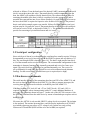
will send or receive 30 bits, as depicted in Table (3.1.) . The routines described herein
provide for converting a byte into this format and vice-versa.
3.2 Serial port configuration
rsit
yo
Since each byte of data to be exchanged on the serial interface actually requires 30 bits to
be transmitted or received, it has to be split in the SPORT registers into two halves of 15
bits. The word-length SLEN is therefore set to 141. The data is right justified into bits 0
to 14 of the transmit and receive buffer registers. The recommended configuration for the
transmitter is alternate framing mode, internally generated and active low frame sync
signal. The serial clock has of course to be generated internally, too. The receiver is
set up differently for each half. The first half is received in unframed mode (alternate
framing). For the second word, external frame sync is required (active high).
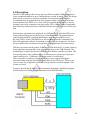
3.3 Hardware requirements
Un
ive
The serial interface consists of the transmitter data line (pin DT0 of the ADMC331) and
the receiver data line (pin DR0 on the ADMC331). In order to generate interrupts, the
receiving data line DR0 must be tied also to the RFS0 pin of the ADMC331.
If shifting from the TTL level (0V and +5V) to UART levels (-10V and +10V) is
required (for instance, when communicating with a PC), some additional hardware is
necessary. The schematic shown in Figure 3.1 makes use of the AD7306 converter. Also,
the DSP side is isolated from the other device by means of standard opto-couplers such as
the HCPL0630.
Of course, the AD7306 is only needed if RS232 voltage levels are required. The isolation
is also optional. The routines presented here could be used to implement an SCI/UART
type interface between processors at TTL voltage levels. In that case, only pull-up
resistors on DT0 and DR0 (RSF0 still has to be tied to DR0) are required.
12
i re
dsh
fo r
ert
Figure 3.1
fH
3.4 The UART Library Routines
3.4.1 Using the UART routines
rsit
yo
The UART routines are developed as an easy-to-use library, which has to be linked to the
user’s application. The library consists of two files. The file “uart0.dsp” contains the
assembly code for the required subroutines. This package has to be compiled and can
then be linked to an application. The user simply has to include the header file “uart0.h”,
which provides function-like calls to the routines.
The routines require some configuration constants, which are declared in a dedicated
section of the main include-file “main.h” that comes with every application note.
Un
ive
In the following sections each routine is explained in detail with the relevant segments of
code which is found in either “uart0.h” or “uart0.dsp”. For more information (e.g. about
register use) see the comments in those files.
The following table 3.2 summarizes the set of macros defined in this library.
Table 3.2
13
i re
dsh
There is an initialization routine UART0_Init that has to be invoked prior to using the
interface. After that data bytes may be sent or received from the host by calling the
routines UART0_Write or UART0_Read, respectively.
3.4.2 The UART interface
fo r
The library may be accessed by including the header file “uart0.h” in the application
code, as was already explained in the previous section.
ert
It expects some constants defined in “main.h”. These are two parameters that the user
may want to modify, namely namely the frequency of the crystal that is used on the board
(CLKIN; defaults to the value on the evaluation board of the ADMC331) and the desires
transfer speed. The constant UART0_Baudrate defines the latter. Common values for this
parameter are 1200, 2400,…, 115200 [baud/sec]. The configuration values of SPORT0
are then derived from these constants.
fH
The header file gives external access to the UART-routines. It is mostly self-explaining.
The UART routines and header files are in the attached document where the project
related software are attached
yo
Here only short descriptions of how to implement routines is written, the supporting
software are in the last section of the report.
3.4.3 The initialization of SPORT0: UART0_Init_
rsit
The clock speed of the SPORT is calculated from the configuration parameters. You will
note that there is a variable called UART0_Status, which represents the UART status at
every time. This is achieved through six flag bits in the variable. They are defined after
declaration section.
Un
ive
The actual assembly code may be analyzed. The UART0_Init_ subroutine initializes the
SPORT0 registers with the appropriate constants. Then the status flags are all reset,
indicating that there are no pending transmissions and no data has been received. At last,
the routine enables the serial port after clearing any pending (and not desired) interrupt. A
call to this routine is necessary for every application before making use of the UART
interface.
3.4.4 The transmitter routine: UART0_Write_
The transmitter routine makes use of three of the status flags in order to ensure the correct
sequence of the operations. The flag UART0_TransmitBufferNotEmpty indicates that a
previous transmission is still in progress when it is set. It is initially polled until there are
no pending transmissions, i.e. the buffer is empty. At this point the demanded
14
i re
fH
ert
fo r
dsh
transmission may be initiated. The above mentioned flag is set, and two other bits,
namely UART0_FirstWordTransmitted and UART0_SecondWordTransmitted are
cleared to indicate that none of the two words has been transmitted yet. The data byte in
ax0 is processed to generate the two 15-bit words to be sent. The next action that is
required is to send the first word and update the status flag
UART0_FirstWordTransmitted by setting it, which indicates that the first word has been
transmitted. For correct operation under all conditions, these operations may not be
interrupted by any other service routine. This is ensured by the adopted sequence of
disabling any interrupt, performing the two actions and enabling interrupts after that
again. The SPORT will generate an interrupt as soon as it is ready to transmit another
word. This will call the interrupt service routine UART0_TX_Isr, which provides for
sending the 2nd word after checking the status. Again, updating the status and sending
the word is not interruptible by means of the sequence described above. This time the
flag UART0_SecondWordTransmitted is set. The SPORT will generate another interrupt
when ready for the next transmission. Now, since the status indicates that both halves are
sent, no further transfer is required and the UART0_TransmitBufferNotEmpty is cleared
to indicate that the next transmission may be started.
The routine UART0_Write_ is the, globally accessible, entry point, which initiates the
transmission of the data contained in the low-byte of ax0.
yo
3.3.5 The receiver routine: UART0_Read_
rsit
The transmitter routine makes use of three of the status flags in order to ensure the correct
sequence of the operations. The flag UART0_ReceiveBufferFull indicates that a
complete 30-bit word has been received and is ready to being processed, when it is set. It
is initially polled until a word is received, i.e. the buffer is full. At this point the data byte
is extracted from the 30-bit word and stored into ax0. The status is reset to indicate that
the routine is ready for a new operation. Unlike the transmitter, the receiving routine has
no control over the start of the data transfer. When a word is received the SPORT
generates an interrupt. Depending on the status of the flags, namely
Un
ive
UART0_FirstWordReceived and UART0_SecondWordReceived, the service routine
undertakes different actions. When UART0_FirstWordReceived is cleared, indicating
that none of the two words has been received yet, the word is stored in RX0A, SPORT0
is set up in the receiving mode for the second half and the status is updated. If the flag
UART0_SecondWordReceived is cleared, the word goes to the second half RX0B,
SPORT0 is set up in the receiving mode for the next first half and the status is updated. If
none of the above conditions is true then the currently received word was received before
Read_UART0 has processed the previous words. In that case, the word is removed from
the SPORT0 receive register and is lost for any further operation.
The routine UART0_Read_ is the, globally accessible, entry point, which waits for data
to be received over SPORT0. It then extracts the data-byte and stores the in the low-byte
of ax0.
15
i re
The software section also contains the codes for generating the PWM.
dsh
The comments are given in the codes where they are required to explain the necessary
steps
3.5 Receiver configuration
Un
ive
rsit
yo
fH
ert
fo r
As mentioned , the interface requires a different SPORT configuration for each halve of
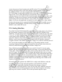
the received word. The reason for this is explained by means of a measured timing
diagram, such as shown in Figure . The represented relation between serial clock and data
receive line is only indicative since data is transmitted asynchronously from the host.
The receiver is initially set up with the RFSR (receive frame sync required) bit equal to
zero. This entails that the frame sync signal (tied to data receive line) is required only at
the beginning of the data acquisition. Therefore, a continuous stream of data would be
read in. When the first halve is read, SPORT0 generates an interrupt (the first glitch of
the bottom track in the figure below) and starts reading the next bits. The interrupt routine
now changes the configuration by setting the RFSR bit. SPORT0 will from now on only
acquire data if a new frame sync signal is applied. However, the current word (the 2nd
halve) is still read. When this word is completely transferred, a second interrupt is
generated and the service routine resets the RFSR bit to the initial condition. The UART
specification requires the DR0 line to be held high. SPORT0 will only recognise a new
frame sync signal when is goes low again, which is when the start-bit of the next data is
sent (…..).
16
i re
dsh
fo r
ert
fH
yo
Typical timing diagram during receive operation. Top: serial clock SCLK0; MID: data
receive DR0; BOTTOM: execution of the interrupt service routine UART0_RX_Isr.
rsit
3.6 Reliability of the communication
Un
ive
Since the process of receiving is, due to the nature of the SPORTs, trying to synchronize
an inherently asynchronous signal to the internal serial clock, certain misinterpretations
cannot be avoided with these simple, three-times over sampling, routines. The falling
edge of the start-bit may fall anywhere within one cycle of the serial clock. The receiver
then stores 30 bits on the falling edges of the serial clock. However, if the falling edge of
the start-bit coincides with the falling edge of the clock, that bit may be erroneously read
in and the whole word is anticipated by one bit. This may lead to incorrect interpretation.
Tests have shown that this occurs with a probability of approx. 80ppm, when data is
continuously sent. The probability decreases drastically if delays are inserted between the
single bytes to be transmitted.
In order to avoid unacceptable behaviors, it is recommended to echo the received data to
the host, which should check for eventual misinterpretation.
If a more robust transmission is required, the three-times sampling is not suited. One may
think of increasing the sampling factor to 5 or 6. This entails more complicate routines
since more words have to be read and sent for each byte, but on the other hand allow for
17
i re
error detection and correction by testing more samples for each bit and implementing
some kind of majority tests.
dsh
3.7 Interrupt configuration and context swapping in ADSP2100
Un
ive
rsit
yo
fH
ert
fo r
As mentioned in preceding sections, it has been decided to use the primary set of registers
in the interrupt service routines and to manually save the context rather than swapping to
the secondary set provides with the ADSP-21xx core. The reason for it is that serial
communication tasks are normally strongly linked to main loop routines. Since there is
only one register that is required by the service routines, the overhead created by the
context saving instruction is not critical. The advantage of this approach is that the option
of nesting interrupts, such as PWM service routines with the serial communication
routine is left to the user of this interface. As shown in the example, the PWM routine
swaps the set of registers, and may be nested with the serial interrupts with no additional
code.
18
i re
dsh
Chapter # 4
UNIVERSAL SERIAL BUS (USB)
fo r
1. An external peripheral interface standard for communication between a
computer and external peripherals over a cable using bi-serial transmission.
fH
ert
2. Universal Serial Bus) a plug-and-play interface between a computer and
add-on devices (such as keyboards, phones and PDAs). With USB, a new
device can be added to a computer without having to add an adapter card or
even having to turn the computer off. USB supports a data speed of 12
megabits per second and is now being incorporated in some cell phones
which is useful for synchronizing information with a computer or
downloading ringtones.
Un
ive
rsit
yo
4.1 USB 245M
19
i re
4.2 Description
fo r
dsh
The DLP-245M USB provides an easy and cost effective method of transferring data to
/from a peripheral and host at up to 8 million bits per second. Its simple FIFO- like design
makes it easy to interface to any microcontroller or microprocessor via I/O ports.
To send data from the peripheral to the host computer simply write the byte wide data
into the module when TXE# is low. If the (384 byte) transmit buffer fills up or is busy
storing the previously written byte, the device takes TXE # high in order to stop further
data from being written until some of the FIFO data has been transferred over USB to the
host.
ert
When the host sends data to the peripheral over USB, the device will take RXF# low to
let the peripheral know that at least one byte of data is available. The peripheral then
reads the data until RXF #goes high indicating no more data is available to read.
By using FTDI’s virtual COM Port drivers, the peripheral looks like a standard COM
Port to the application software. Commands to set the baud rate are ignored – the device
always transfers data at its fastest rate regardless of the application’s baud rate setting.
yo
fH
USB devices transfer data in packets. If data is to be sent from the PC, a packet is built up
by the application program and is sent via the device driver to the USB scheduler. This
scheduler puts a request onto the list of tasks for the USB host controller to perform. This
will typically take at least 1 millisecond to execute because it will not pick up the new
request until the next ‘ USB Frame’ (the frame period is 1 millisecond).
There is therefore a sizeable overhead (depending on your required throughput)
associated with moving the data from the application to the USB device. If data is sent
‘byte at a time’ by an application, this will severely limit the overall throughput of the
system as a whole.
Un
ive
rsit
It must be stressed that in order to achieve maximum throughput, application programs
should send or receive data using buffers and not individual characters.
20
i re
Un
ive
rsit
yo
fH
ert
fo r
dsh
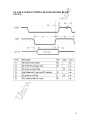
4.2.1 DLP-USB 245 TIMING DIAGRAM-FIFO READ
CYCLE
21
i re
Un
ive
rsit
yo
fH
ert
fo r
dsh
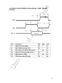
4.2.2 DLP-USB TIMMING DIAGRAM –FIFO WRITE
CYCLE
22
i re
Un
ive
rsit
yo
fH
ert
fo r
dsh
4.3 USB Pin configuration
23
24
ert
fH
yo
rsit
Un
ive
fo r
dsh
i re
i re
4.4 USB I/O Programming
dsh
4.4.1 Introduction
This document describes how to communicate to the USB I/O device.
4.4.2 Requirements
ert
fo r
USB IO Device
I/O USB Driver
USB ready computer running Win98, ME or 2K
Microsoft Visual C++ version 4.0 or better, or equivalent 32 bit compiler for x86 based
system, or Visual basic
Knowledge of C or Visual basic
4.4.3 Overview
yo
fH
To communicate with USB IO Driver one must first enumerate thedevice. The
enumeration of the device returns a device name. This device name is used to open the
interface, using CreateFile(). Once you have the handle from CreateFile() you can use
DeviceIOControl() to communicate to the USB IO Device and CloseHandle() to close it.
The hardest part is getting the device name the rest is simply. To send commands to the
USB IO device simply build a command packet and submit it using the DeviceIOControl
functions.
4.5 Device Enumeration:
Un
ive
rsit
In order to communicate to the USB device one must first find its device name. The
device name consists of a number representing a physical port plus the GUID (global
unique identifier) for the device. The current USB port and the GUID are combined to
form the device name. The device name can change each time you plug in an additional
device or plug the device into a different USB port or hub on your computer. The typical
complete device name looks like
\\.\0000000000000012#{b5157d69-75f8-11d3-8ce0-00207815e611}.
In Windows XP a typical device name look like
\\.\USB#Vid_0FC5&Pid_1222#000000001#{b5157d69-75f8-11d38ce0-00207815e611}.
4.6 Device Name Registry Method
There are two ways to get the device name. The easiest method is to read the device name
from the registry. When a USB I/O device is plugged in to your computer, the OS detects
it and loads the driver. When this driver loads the device name is stored in the registry.
Then the user just reads the name out of the registry. This method has one disadvantage.
It can’t be used when more than one USB I/O device is plugged in to your computer,
because only the last device name will be recorded in the registry. To use the registry
method simply open the registry key, query the value, and close the registry key. The
registry key name is Device Name and the path is
HKEY_LOCAL_MACHINE\System\CurrentControlSet\Services\........\USB\Parameters\
25
i re
You can uses regedit.exe to find the entry. It also a good place to copy the GUID from so
you don’t any mistakes.
rsit
yo
fH
ert
fo r
dsh
VB Registry Example
Here is an example in Visual Basic on how to read the device name
from the registry.
DIM DeviceName as string
DeviceName = GetRegValue(HKEY_LOCAL_MACHINE, _
"System\CurrentControlSet\Services\.......\USB\Parameters\", _
"DeviceName")
' GetRegValue - Gets the Key value in the registry given a registry key.
Function GetRegValue(hKey As Long, lpszSubKey As String, szKey As String ) As
String
Dim phkResult As Long, lResult As Long
Dim szBuffer As String, lBuffSize As Long
'Create Buffer
szBuffer = Space(255) ' Allocate buffer space
lBuffSize = Len(szBuffer) ' Set the length
RegOpenKeyEx hKey, lpszSubKey, 0, 1, phkResult 'Open the Key, get a handle to it
lResult = RegQueryValueEx(phkResult, szKey, 0, 0, szBuffer, lBuffSize) 'Query the
value
RegCloseKey phkResult 'Close the Key
If lResult = ERROR_SUCCESS
Then
GetRegValue = szBuffer ‘ return key value
End If
Exit Function
4.7 Device Name Enumeration Method
Un
ive
The second method to get the device name is two use Windows™ device manger. To do
this one calls a function in the setupapi.dll.Simply poll the device manger with the USB
I/O GUID for all the devices that match the GUID given. The device manger will return
the device names for all the devices currently available on your system. This is the better
way of getting the device name. It allows the user to use multiple devices on the same
computer. The draw back is that it is little more complicated.
C Enumeration Example
Below is a C example using this enumeration method.
Use the DEFINE_GUID macro to build the GUID.
// {B5157D69-75F8-11d3-8CE0-00207815E611}
DEFINE_GUID(USB_GUID, 0xb5157d69, 0x75f8, 0x11d3, 0x8c, 0xe0, 0x0, 0x20,
0x78, 0x15, 0xe6, 0x11);
This GUID is passed to SetupDiGetClassDevs(), which returns a handle to the device.
The enumeration functions are found in the setupapi library.
HDEVINFO hinfo = SetupDiGetClassDevs(&USB_GUID, NULL,
NULL, DIGCF_PRESENT | DIGCF_INTERFACEDEVICE);
26
i re
Un
ive
rsit
yo
fH
ert
fo r
dsh
The first argument identifies the interface you’re looking for. The flag bits in the last
argument indicate that you are looking for the interfaces exported by the USB I/O device.
Once you have a handle to the device information set, you can perform an enumeration of
all the devices that export the particular interface you’re interested in. See Microsoft
function documentation for more information on setupapi.dll library functions. Poll the
device manager till there are no matching devices left.
int i;
Cstring Devices[10]; // an array of cstrings for (DWORD i=0; ; ++i)
{
SP_INTERFACE_DEVICE_DATA Interface_Info;
Interface_Info.cbSize = sizeof(Interface_Info); // Enumerate device
if (!SetupDiEnumInterfaceDevice(hInfo, NULL, (LPGUID) &USB_GUID,i,
&Interface_Info))
{
SetupDiDestroyDeviceInfoList(hInfo);
return(i);
}
DWORD needed; // get the required lenght
SetupDiGetInterfaceDeviceDetail(hInfo, &Interface_Info,
NULL, 0, &needed, NULL);
PSP_INTERFACE_DEVICE_DETAIL_DATA detail =
(PSP_INTERFACE_DEVICE_DETAIL_DATA) malloc(needed);
if (!detail)
{
SetupDiDestroyDeviceInfoList(hInfo);
return(i);
}
// fill the device details
detail->cbSize =
sizeof(SP_INTERFACE_DEVICE_DETAIL_DATA);
if (!SetupDiGetInterfaceDeviceDetail(hInfo,
&Interface_Info,detail, needed,NULL, NULL))
{
free((PVOID) detail);
SetupDiDestroyDeviceInfoList(hInfo);
return(i);
}
char name[MAX_PATH];
strncpy(name, detail->DevicePath, sizeof(name));
free((PVOID) detail);
Devices[i] = name; // keep a copy of each device name
} // end of for loop
After this code runs you end up with a list of device names, or NULL if no devices could
be found (i = 0). Each device name will represent one USB I/O device that is plugged
into your computer. If you know that you will only support one USB I/O device on your
system at one time, you can reduce the enumeration code by dropping the for loop and
27
i re
4.8.1 Open Device
fo r
4.8 Device Communications:
dsh
only going through the code once. The device name(s) that are returned from the above
code have a port number prefixed to the original GUID. The port number is related to
order of the plug and play devices on your machine and can not be predetermined. The
device name should look like the following.
\\.\0000000000000012#{b5157d69-75f8-11d3-8ce0-00207815e611}
This is the complete device name one will use in order to communicate with the USB I/O
device.
fH
ert
To begin communicating with the USB I/O device you must first acquire a handle to it.
To do this just pass the device name to the CreateFile() function. This is done in the same
manner as opening or creating a file. If successful, this function will return a handle to the
device. If the device is not plugged in, un-powered, or opened by another program this
function will fail.
4.8.2 Device Close
yo
HANDLE hUsbDevice = CreateFile(devicename, GENERIC_READ |
GENERIC_WRITE, 0, NULL, OPEN_EXISTING, 0, NULL);
rsit
When your application has finished using the device, the device should be closed. To do
this call CloseHandle() with the device handle. If you do not close the device, you will
not be able to access it again without re-setting the device port.
CloseHandle( hUsbDevice ) ;
4.9 Device Communications
Un
ive
4.9.1 Device I/O Control
The DeviceIOControl() function provides the communication method between the users
and the device. This function accepts CTL_CODES and users buffers that are passed to
the device driver and eventually the USB device.
success = DeviceIoControl(hUsbDevice, IOCTL_USB_SEND_PACKET, &TxPacket,
8+TxPacket->Length, &RxPacket, 8, &nBytes, NULL);
The CTL Codes are predefined codes that describe the action to take place. There are
many different codes but for our purposes we are only concerned with the send packet
code.
Below is the CTL_CODE generation shown in C.
#define CTL_CODE( DeviceType, Function, Method, Access ) ( \
28
i re
ert
fo r
dsh
((DeviceType) << 16) | ((Access) << 14) | ((Function) << 2) | (Method))
#define METHOD_BUFFERED 0
#define FILE_ANY_ACCESS 0
#define FILE_DEVICE_UNKNOWN 0x00000022
// --------------------------------------------------------- //
#define FTDI_USBIO_IOCTL_VENDOR 0x0800 // Vendor defined
#define IOCTL_USB_WRITE_PACKET CTL_CODE(FILE_DEVICE_UNKNOWN, \
FTDI_USB_IOCTL_VENDOR+10,\
METHOD_BUFFERED, \
FILE_ANY_ACCESS)
The above code generates a CTL_CODE of 0x222028. You can just
use this number instead for using the above code, see below. For VB
code use &H222028.
#define IOCTL_USBIO_SEND_PACKET 0x222028 // for C
Const CTL_CODE_SEND_PACKET = &H222028 ‘ for VB
yo
fH
Once you have the CTL_CODE the next step is to make the command packet. This is a
simply structure of which you just set the fields for a particular command. The fields in
the command packet are described in the USB IO Data Sheet. Simply fill the structure
and send it to the USB device with the DeviceIOControl function. For read commands
the DeviceIOControl function returns the data in the RxPacket. The length of the sent
packet can range from 8 to 16 bytes. The received packet is always 8 bytes long. The
length data member of the send packet is the length of the data extension. The data
extension is only required by certain commands. If the data extension member is not
being used set the data extension length to zero.
Un
ive
rsit
The packet command structure consists of the following elements.
// Command Packet Structure define in C
typedef struct _ioPacket{
unsigned char Recipient;
unsigned char DeviceModel;
unsigned char MajorCmd;
unsigned char MinorCmd;
unsigned char DataLSB;
unsigned char DataMSB;
unsigned short Length; // length of data extension
unsigned char DataExtension[8];
} VENDORPACKET,*PVENDORPACKET;
‘ Command Packet Structure define in VB
Public Type PacketStructure
Recipient As Byte
DeviceModel As Byte
MajorCmd As Byte
MinorCmd As Byte
DataLSB As Byte
DataMSB As Byte
29
i re
dsh
Length As Int ‘ length of data extension
DataEntension(8) As Byte
End Type
yo
fH
ert
fo r
C Example
This C code example sends the packet and receives the data in the
same packet that was sent to it. On error it returns –1.
int UsbCtrl(PVENDORPACKET pPacket)
{
ULONG nBytes;
BOOLEAN Success;
Success = DeviceIoControl(hUsb,
IOCTL_USBIO_WRITE_PACKET,
pPacket, 8+pPacket->Length, pPacket, 8, &nBytes,
NULL) ;
if(!Success ) //|| ( nBytes != sizeof(VENDORPACKET) ) )
{
if(Verbose)MessagePopup ("UsbCtrl Error","DeviceIoControl call failed!");
return(-1);
}
else
return(0);
}
Un
ive
rsit
VB Example
This VB code example sends the packet and receives the data in the
returned value of the function.
'Sends the USB packet to the device
Function SendPacket(ByRef TxPacket As PacketStructure) As PacketStructure
Dim lpResult As Long
Dim RxPacket As PacketStructure
TxPacket.Recipient = 8 ' always 8
TxPacket.DeviceModel = 18 ' always 18
If 0 = DeviceIoControl(hDevice, CTL_CODE_SEND_PACKET, TxPacket,
8+TxPacket.Length, RxPacket, 8, lpResult, 0)
Then
MsgBox "SendPacket() DeviceIoControl Failed."
Exit Function
End If
SendPacket = RxPacket
End Function
4.9.2 Registry Keys:
The following is a list of registry keys that the USB I/O driver adds to the registry. To
access the registry, run RegEdit.exe from the command prompt. The registry keys are
located at:
30
i re
Un
ive
rsit
yo
fH
ert
fo r
dsh
HKEY_LOCAL_MACHINE\System\CurrentControlSet\Services\......\USB\Parameters
USB I/O Registry Keys
• DebugLevel Used for debugging should always be zero.
• BootUpTest Used for testing should always be zero.
• DeviceName This string contains the device name of the last USB IO device loaded.
31
i re
Chapter # 5
Un
ive
rsit
yo
fH
ert
fo r
dsh
Results
The results and the soft wares are attached there are two forms and three .bas files. These
detect the device connected at the USB port of the hub load it drivers and then
communicate with it in order to collect data. The comments before the start of every
statement explain the action of the step.
32
i re
Chapter # 6
dsh
Conclusion
fo r
The design of Interface between PC and DSP module based on the Visual basic has been
shown in this report. There are different ways to design an interface including the other
languages like in C , Java, Assembly Language
ert
The first and foremost thing in order to develop an interface is to get the knowledge of
the hard ware involved .DSP board that we have used belongs to ADMC 2100 family.
This Family has got high transfer rate as compared to other DSP modules. It has got
UART connected to it through nine pin D type connector and it is isolated from rest of
the board The drivers of the DSP and UART are loaded and in return these run the DSP
module and the UART that helps to transfer data via USB.
fH
After the hardware is connected software is developed and implemented one by one.
First of all drivers for DSP and UART have been installed and then program developed in
VB tool to communicate between PC and DSP module. This program contains two
Forms and three modules (.bas files). In data collect form it get the name of the HOST
CONTROLER, ROOT HUB and then open a connection to it.
yo
After that it get node information and save this information in our data table to discover
the connected device to the ports of ROOT HUB.
Un
ive
rsit
Then the control is passed to display form once all the information has been collected and
that DISPLAY FORM will show required information.
33
i re
Un
ive
rsit
yo
fH
ert
fo r
dsh
Bibliography
Related Documents and Web sites
Universal Serial Bus Specification www.usb.org
Microsoft Development Network
www.msdn.microsoft.com
www.msdn.microsoft.com
Delcom Engineering Web Site www.delcom-eng.com
www.delcom
Analog devices user manual
IEE journals and tutorials
34