1
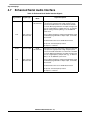
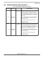
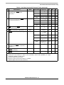
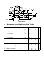
Enhanced Serial Audio Interface Timing
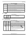
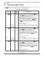
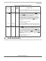
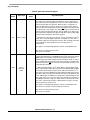
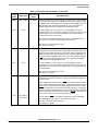
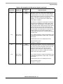
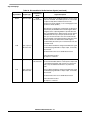
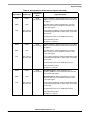
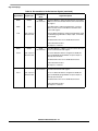
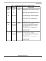
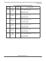
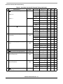
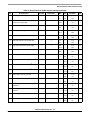
Table 24. Enhanced Serial Audio Interface Timing (continued)
No.
88
89
90
91
Characteristics1, 2, 3
Symbol
Expression3
Min
Max
Condition4
Unit
SCKT edge to transmitter #0 drive enable
deassertion7
—
—
—
14.0
x ck
ns
—
9.0
i ck
FST input (bl, wr) setup time before SCKT
edge6
—
2.0
—
x ck
18.0
—
i ck
FST input (wl) setup time before SCKT
edge
—
2.0
—
x ck
18.0
—
i ck
FST input hold time after SCKT edge
—
4.0
—
x ck
5.0
—
i ck
—
—
—
ns
ns
ns
92
FST input (wl) to data out enable from high
impedance
—
—
—
21.0
—
ns
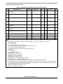
93
FST input (wl) to transmitter #0 drive enable
assertion
—
—
—
14.0
—
ns
94
Flag output valid after SCKT rising edge
—
—
—
14.0
x ck
ns
—
9.0
i ck
95
HCKR/HCKT clock cycle
—
2 x TC
13.4
—
ns
96
HCKT input edge to SCKT output
—
—
—
18.0
ns
97
HCKR input edge to SCKR output
—
—
—
18.0
ns
Note:
1 V
CORE_VDD = 1.25 ± 0.05 V; TJ = -40°C to 110°C (52 LQFP) / -40°C to 105°C (80 LQFP), CL = 50 pF
2 i ck = internal clock
x ck = external clock
i ck a = internal clock, asynchronous mode
(asynchronous implies that SCKT and SCKR are two different clocks)
i ck s = internal clock, synchronous mode
(synchronous implies that SCKT and SCKR are the same clock)
3 bl = bit length
wl = word length
wr = word length relative
4 SCKT(SCKT pin) = transmit clock
SCKR(SCKR pin) = receive clock
FST(FST pin) = transmit frame sync
FSR(FSR pin) = receive frame sync
HCKT(HCKT pin) = transmit high frequency clock
HCKR(HCKR pin) = receive high frequency clock
5 For the internal clock, the external clock cycle is defined by Icyc and the ESAI control register.
6 The word-relative frame sync signal waveform relative to the clock operates in the same manner as the bit-length frame
sync signal waveform, but spreads from one serial clock before first bit clock (same as bit length frame sync signal), until
the one before last bit clock of the first word in frame.
7 Periodically sampled and not 100% tested.
8 ESAI_1 specs match those of ESAI.
DSP56374 Data Sheet, Rev. 4.2
46
Freescale Semiconductor